1
Flash Center Memory Programmer
Supported products:
Features
•
•
•
•
•
•
•
•
•
Support for many popular I2C EEPROM devices
Support for many popular SPI EEPROM and flash devices
Parallel, gang programming of devices
Loads and saves Binary, Intel Hex and Motorola S-Record formats
High-speed SPI programming with the Promira Serial Platform and
Cheetah SPI Host Adapter
High-speed Multi I/O SPI programming with the Promira Serial
Platform
Custom devices supported through user-specified XML
Linux and Windows compatible
Freely available for use with Promira Serial Platform, Cheetah SPI
Host Adapter, and Aardvark I2C/SPI Host Adapter
Summary
The Flash Center software is a graphical application for programming
serial memory devices. It provides an easy-to-use interface for
programming a wide variety of target EEPROM and flash chips.
Multiple target devices can be programmed in parallel. This software
is freely available for use with the Promira Serial Platform, Cheetah
SPI Host Adapter, and Aardvark I2C/SPI Host Adapter sold by Total
Phase.
Flash Center
User Manual v1.43
November 20, 2015
Flash Center User Manual v1.43
1 Overview
The Total Phase Flash Center provides a convenient method to program one or more
serial memory devices simultaneously. It is intended to be used with the Promira Serial
Platform, Cheetah SPI Host Adapter, and Aardvark I2C/SPI Host Adapter sold by Total
Phase. The operation of these host adapters is described in detail in their respective
manuals. The Flash Center application is written using the standard Promira Serial
Platform, Cheetah SPI Host Adapter, and Aardvark I2C/SPI Host Adapter APIs, which
are freely available on the Total Phase website: http://www.totalphase.com/.
The Promira Serial Platform can function as an I2C/SPI master/slave device. It can
communicate up to 80 MHz on SPI, and up to 1 MHz on the I2C bus. The Aardvark I2C/
SPI Host Adapter can function as an I2C/SPI master/slave device. It can communicate
up to 8 MHz on SPI, and up to 800 kHz on the I2C bus. The Cheetah SPI Host Adapter
can function as an SPI master device. It is capable of communicating up to 40+ MHz.
Information about the Promira Serial Platform, Cheetah SPI Host Adapter, and Aardvark
I2C/SPI Host Adapter and the APIs used to program them can be found on the Total
Phase website.
With these adapters, an end-user can use the Flash Center to program I2C EEPROMs,
SPI EEPROMs, and SPI flash devices.
1.1 Changes in version 1.43
The following new features have been added to Flash Center.
The Flash Center v1.43 supports the Promira FW v1.33 and up.
Memory Device Files
• Added the following devices to the parts library:
◦ Micron N25Q128A 1.8V 16 Megabyte SPI Flash
1.2 Changes in version 1.42
The following new features have been added to Flash Center.
The Flash Center v1.42 supports the Promira FW v1.32 and up.
Bug Fixes
• Fixed the connectivity issue of the first attempt to connect the Promira platform to
Flash Center after the device reset.
2
Flash Center User Manual v1.43
1.3 Changes in version 1.41
The following new features have been added to Flash Center.
Memory Device Files
• Added the following devices to the parts library:
◦ Cypress CY14MB064J 8 KByte I2C nvSRAM
• Updated the maximum bitrate for the following devices in the parts library:
◦ Micron N25Q032A 4 Megabyte SPI Flash (80MHz)
◦ Micron N25Q128A 16 Megabyte SPI Flash (80MHz)
◦ Micron N25Q512A 64 Megabyte SPI Flash (80MHz)
◦ Micron N25Q00AA 128 Megabyte SPI Flash (80MHz)
◦ Spansion S25FL128S 16 MB SPI Flash, 64 KB sectors (80MHz)
◦ Spansion S25FL128S 16 MB SPI Flash, 256 KB sectors (80MHz)
◦ Spansion S25FL256S 32 MB SPI Flash, 64 KB sectors (80MHz)
◦ Spansion S25FL256S 32 MB SPI Flash, 256 KB sectors (80MHz)
◦ Spansion S25FL512S 64 MB SPI Flash, 256 KB sectors (80MHz)
◦ SST SST25VF064C 8 Megabyte SPI Flash (75MHz)
Bug Fixes
• Fixed the crash issue when two memory parts are connected simultaneously with
different SPI IO mode each.
• Fixed the issue with the Promira Serial Platform with I2C only licensed or SPI only
licensed.
1.4 Changes in version 1.40
The following new features have been added to Flash Center.
3
Flash Center User Manual v1.43
Memory Device Files
• Added the following devices to the parts library:
◦ Micron N25Q032A 4 Megabyte SPI Flash (Dual, Quad)
◦ Micron N25Q512A 64 Megabyte SPI Flash (Dual, Quad)
◦ Micron N25Q00AA 128 Megabyte SPI Flash (Dual, Quad)
◦ Spansion S25FL128S 16 MB SPI Flash, 64 KB sectors (Dual, Quad)
◦ Spansion S25FL128S 16 MB SPI Flash, 256 KB sectors (Dual, Quad)
◦ Spansion S25FL256S 32 MB SPI Flash, 64 KB sectors (Dual, Quad)
◦ Spansion S25FL256S 32 MB SPI Flash, 256 KB sectors (Dual, Quad)
◦ Spansion S25FL512S 64 MB SPI Flash, 256 KB sectors (Dual, Quad)
◦ SST SST25VF064C 8 Megabyte SPI Flash (Dual)
• SPI I/O Mode parameters added to configure SPI I/O mode for the address and
data:
◦ dualIO
◦ quadIO
◦ ioModeAddress
◦ ioModeDataIn
◦ ioModeDataOut
1.5 Changes in version 1.31
The following new features have been added to Flash Center.
• Updated UI to control target power, IO Power, and level shift for the Promira
Serial Platform.
4
Flash Center User Manual v1.43
• Updated UI to configure custom IP addresses for the Promira Serial Platform.
1.6 Changes in version 1.30
The following new features have been added to Flash Center.
• Support Promira Serial Platform.
1.7 Changes in version 1.24
The following new features have been added to Flash Center.
Memory Device Files
• Added the following devices to the parts library:
◦ Catalyst CAT93C56 256 Byte SPI EEPROM
◦ Macronix SPI flash parts
• SPI protocol parameters added to give Flash Center much more flexibility:
◦ spiMode
◦ spiBitorder
◦ spiSSPolarity
1.8 Changes in version 1.23
The following new features have been added to Flash Center.
New Features
• Added the ability to save user preferences.
• Added the ability to check for software updates.
Bug Fixes
• Fixed the error on saving data in SRecord format that couldn't save bigger than
2Mbytes.
• Fixed the error on saving data in binary format that appends wrong extension
which is 'a.hex'.
5
Flash Center User Manual v1.43
Memory Device Files
• Added the following device families to the parts library:
◦ Micron N25Q512A 64 Megabyte SPI Flash
◦ Micron N25Q00A 128 Megabyte SPI Flash
1.9 Changes in version 1.22
The following new features have been added to Flash Center.
Bug Fixes
• Fixed overflow problems with large (256 Mb+) memory devices.
Memory Device Files
• SST Auto Address Increment (AAI) programming support added:
◦ writeAutoAddressIncrementInstruction
◦ writeAutoAddressIncrementSize
◦ writeAutoAddressIncrementTime
• SST flash memory file added to parts library.
• Added enable extended addressing (4B) mode instruction for large SPI memory
devices:
◦ extendedAddressingEnableInstruction
• User-definable transaction parameters added to give Flash Center much more
flexibility:
◦ userTransaction1
◦ userTransaction2
◦ userTransaction1WriteEnable
◦ userTransaction2WriteEnable
◦ userTransaction1Time
◦ userTransaction2Time
6
Flash Center User Manual v1.43
1.10 Changes in version 1.21
The following new features have been added to Flash Center.
Bug Fixes
• Fixed an error with the Microchip 24LC22A device file.
Memory Device Files
• New device parameters added to support a broader range of memory devices:
◦ autoPageUpdate
• Added support for the following devices:
◦ ISSI IS24C04 I2C EEPROM.
◦ Spansion S25FL-A SPI flash parts
◦ Spansion S25FL1/FL2-K SPI flash parts
◦ Spansion S25FL-S/P SPI flash parts
◦ Micron N25Q SPI flash parts
1.11 Changes in version 1.20
The following new features have been added to Flash Center.
Bug Fixes
• Fixed a problem when reading certain I2C EEPROMs greater than or equal to
32 KB in capacity.
• Fixed S-Record file checksum calculation.
• I2C address is no longer limited by the base address.
New Features
• Added support for 64-bit Windows. Note that Flash Center will run on 64-bit
systems as a 32-bit application.
• Intel Hex and S-Record files will not be loaded if they have incorrect checksums.
• Rare Intel Hex record types will cause a warning, but still load successfully.
7
Flash Center User Manual v1.43
Memory Device Files
• New device parameters added to support a broader range of memory devices:
◦ eraseBeforeWrite
◦ pageShift
• Updated the Atmel 45 series devices to write without erasing.
• Updated the Microchip 24xx1025 devices to fix an error with writing.
1.12 Changes in version 1.10
The following new features have been added to Flash Center.
Bug Fixes
• Added support for loading a wider array of S-Record files.
• Fixed operation timeout issue with certain memory devices.
New Features
• Added program without erase option for SPI flash devices.
• Fill feature allows users to specify a data pattern to insert into the hex editor.
• Users may specify a data pattern to fill undefined memory regions when loading
Intel Hex or Motorola S-Record files.
• In adapters panel, Select All and Unselect All buttons added.
Memory Device Files
• When loading memory device files, parts with duplicate device names now
overwrite previous entries instead of being disregarded.
• Added the following device families to the parts library:
◦ Atmel26xxxx SPI flash family
◦ Intel SPI flash devices
◦ ISSI I2C EEPROM parts
◦ Renesas I2C and SPI EEPROM devices
8
Flash Center User Manual v1.43
◦ Samsung I2C EEPROM parts
◦ Seiko I2C EEPROM devices
◦ Xicor I2C EEPROM family
• New device parameters added to support a broader range of memory devices:
◦ writeStatusRegisterEnableInstruction
◦ writeBufferInstruction
◦ deviceConnectedMask
9
Flash Center User Manual v1.43
2 Getting Started
2.1 Requirements
2.1.1 Overview
The following sections describe the requirements to run Flash Center. Be sure the
device driver has been installed before plugging in a Total Phase device. Refer to the
device's manual for additional information regarding the driver and compatibility.
2.1.2 Windows
The Flash Center software is compatible with 32-bit and 64-bit versions of Windows 7,
Windows 8, and Windows 8.1. The software will run on 64-bit systems as a 32-bit
application. Windows XP, Vista, 2000 and legacy 16-bit Windows 95/98/ME operating
systems are not supported.
2.1.3 Linux
The Flash Center software has been designed for Red Hat Enterprise Linux 5 with
integrated USB support. Kernel 2.6 is required. Other distributions, including Ubuntu,
Fedora, and SuSE have also been known to work. The software will run on 64-bit
systems as a 32-bit application, provided that 32-bit system libraries are available.
2.2 Installing the Flash Center Software
The Flash Center software is a self-contained application. Installing the software is as
easy as unpacking the archive containing the software package. To install the Flash
Center:
1. Download the latest version of the software from the Total Phase website.
2. Unzip the zip archive to your desired location.
2.3 Launching the Flash Center
2.3.1 Linux
1. Go to the installation directory where the software package was unzipped.
2. Run >./Flash-Center-GUI
10
Flash Center User Manual v1.43
2.3.2 Windows
1. Go to the folder where the software package was extracted.
2. Double-click on "Flash-Center-GUI.exe"
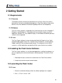
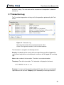
After launching the Flash Center, you will see the screen in Figure 1.
Figure 1 : Initial Screen
After first launching the Flash Center, the software needs to
be connected to at least one Promira platform, Cheetah or
Aardvark adapter.
To program a memory device, the Flash Center software must be connected to at least
one Promira platform, Cheetah or Aardvark adapter. When an adapter is connected to
11
Flash Center User Manual v1.43
the software, it will be unavailable for use by another process until the adapter is
disconnected within the Flash Center or the application is terminated.
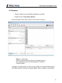
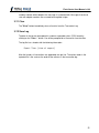
2.4 Add Adapters
To connect to adapters to be used for programming, select File | Add Devices from the
menu, or click the "Add Devices" button.
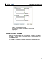
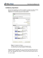
Figure 2 : Add Adapters Dialog
Displays a list of available adapters, their version
information, and serial numbers.
The Add Devices dialog (Figure 2 ) has a list of available adapters and their version
information.
2.4.1 List of Available Adapters
In the Add Devices window, there is a list of all the available Promira platforms, Aardvark
and Cheetah adapters that are connected to the computer. If no adapters appear in the
list, then there are no available units connected to your computer.
Please note that adapters that are in use by other applications are listed as "IN USE".
They are no longer available for use by this current instance of Flash Center. Adapters to
which the Flash Center are already connected will be marked as "IN USE" as well.
The list of adapters provides the following information:
12
Flash Center User Manual v1.43
Port: The port that the adapter occupies. The port number is a zero-based number for
the Aardvark and Cheetah adapters and the port number for the Promira Serial Platform
is an IP address. For more information about USB port assignments, please consult the
appropriate sections of the Promira Serial Platform, Aardvark I2C/SPI Host Adapter, and
Cheetah SPI Host Adapter manuals. Note that if there are both Cheetah and Aardvark
adapters connected to your computer, the Aardvark adapters will be listed first, with port
numbers starting at zero, then the Cheetah adapters will be listed, with port numbers
again starting at zero.
Firmware Version (FW) & Hardware Version (HW): The version numbers of the
adapter. For the Promira platform, the Flash Center shows two version numbers, the first
one is the system firmware version number and the second is the application firmware
version number. For more information about version numbers, please consult the
Promira platform, Aardvark adapter, and Cheetah adapter manuals.
Serial Number: The unique serial number of the adapter. This serial number is unique
across both Promira platform, Aardvark and Cheetah adapters. For the Promira platform,
the same serial number might be shown twice, however the IP address should be
different. Since the Promira platform supports two communication channels, Ethernet
and Ethernet over USB, the Flash Center may find one device from two different
channels.
Custom IPs: Since the Promira platform communicates through Ethernet protocol, the
Promira platform can be accessible from anywhere. However the Flash Center scans
Promira platforms connected directly. For instance, the Promira platform is plugged to
Ethernet at a place and its IP address is visible from other place, a host PC at other
place can access this Promira platform even though the Flash Center cannot find it. For
this case, user can specify the custom IP address to look for. More than one IP address
can be specified. Each IP address should be separated by a comma(',') or a space. This
information is save in the preference file.
2.4.2 Refresh List
To see an updated list of adapters attached to the computer, simply click on the
"Refresh" button to rescan the USB bus or the network.
2.4.3 Opening Adapters
Select one or more devices from the list, using the Shift or Control keys to select multiple
adapters. Then click "Add" to connect to the desired adapter(s). You can also doubleclick on an entry in the list to open a single adapter.
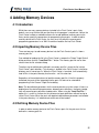
After connecting to one or more adapters, the status bar text at the bottom will change
from "Disconnected" to "Connected." The connected adapters will appear in the Adapter
list, as seen in Figure 3.
13
Flash Center User Manual v1.43
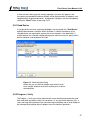
Figure 3 : Connected Adapters Panel
After adapters are connected, they appear in the connected
adapters panel.
2.5 Disconnecting Adapters
Adapters can be disconnected from the current application. To remove a single adapter,
click the red "X" next to the adapter in the Adapters panel. To remove all adapters, click
the "Remove All" button.
After an adapter is disconnected, it becomes available for use with other applications.
14
Flash Center User Manual v1.43
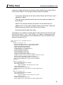
2.6 Selecting Memory Devices
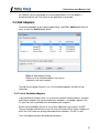
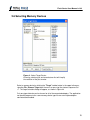
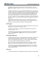
Figure 4 : Select Target Device
Choosing a device type and manufacturer first will simplify
the selection of the part number.
Select a memory device by clicking the "Target" toolbar button in the upper left corner,
selecting File | Choose Target from the menu, or pressing the shortcut sequence Ctrl
+T. The target selection dialog will appear, as shown in Figure 44.
Only one type of device can be chosen for all of the connected adapters. The application
can parallel program to the same memory device type if there are multiple adapters
connected and enabled.
15
Flash Center User Manual v1.43
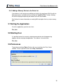
2.6.1 Adding a Memory Device to the Parts List
If your device is not listed you can add the part to the list by creating an XML file with the
device parameters and load the file by clicking the "Load Part File..." button. A dialog
will then be displayed requesting the location of the file to be loaded.
See Section 4 for more information on creating XML description files for custom memory
parts.
2.7 Exiting the Application
To exit the application, go to the menu item:
File | Quit
2.8 Starting Over
It is possible to clear the currently selected memory device and all programming
adapters without restarting the application. The shortcut is the menu item:
File | New
2.9 Preferences
The preferences dialog (Figure 5) allows the user to configure the Flash Center
software. To do so, go to the menu item: Help | Preferences.
16
Flash Center User Manual v1.43
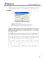
Figure 5 : The preferences dialog
Configure Flash Center options.
2.9.1 Updates
To adjust the frequency that the Flash Center checks for software updates, choose
Daily, Weekly, Monthly, or Never from Updates.
To check for an update manually, click Check Now.
Note: To check for updates, your PC must be connected to the Internet.
2.9.2 User Feedback
Allow Flash Center to collect anonymous usage statistics for improving future versions of
the software.
17
Flash Center User Manual v1.43
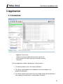
3 Application
3.1 Introduction
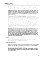
Figure 6 : Flash Center
Adapters have been added and the memory device has
been selected. The flash center can now perform memory
operations.
The main application window is divided into six major sections.
1. The toolbar provides access to all device operations.
2. The "Status" panel provides visual feedback of the overall progress of a
programming operation.
3. The "Device Control" panel shows the current target memory device and allows
the changing of the parameters used to program the device.
18
Flash Center User Manual v1.43
4. The "Adapters" panel shows the adapters that are currently connected and their
individual status. There are also controls to change the target power for each
connected adapter. The enable checkboxes allow the user to select which
adapters will participate in the upcoming programming operations.
5. The "Data" panel contains controls to manipulate the data that will be transferred
to the device. A hex editor is provided for convenience.
6. Finally, the "Transaction Log" panel displays status details for every operation.
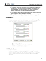
3.2 Adapters
The connected adapters panel shows which adapters are currently in use by the Flash
Center. Each adapter is numbered and has several controls associated with it.
Figure 7 : Adapters Panel
Displays attached adapters and contains controls with
which to manipulate the attached adapters.
3.2.1 Adapter Number
Each connected adapter is numbered, starting from 1. If an adapter is removed,
previously connected adapters will retain their original numbers. When a subsequent
adapter is added, numbering will continue from after the highest number adapter
connected.
19
Flash Center User Manual v1.43
3.2.2 Checkbox
The checkbox next to each adapter allows connected devices to be selected for
participation in a memory operation. Adapters are checked by default when added. They
can become unchecked manually by the user or automatically by the software when the
selected memory device requires a communication protocol not available in a given
adapter (e.g., an I2C memory device is chosen and a Cheetah adapter is present in the
Adapters panel).
The All check and uncheck buttons at the bottom of the adapter's panel will check and
uncheck, respectively, all of the adapters, except those that do not support the selected
memory device's protocol.
3.2.3 Remove Button
The remove button appears as a red "X" (Figure 7 ). Clicking the red "X" will disconnect
the adapter and remove it from the list of connected adapters. To disconnect from all
adapters at once, click the "Remove All" button.
3.2.4 All power on/off
Since memory devices may be programmed in-system, the user has the option of
powering a device from the adapter or externally. Turning on target power or IO power
for a device indicates that the device will be powered by the Promira, Aardvark or
Cheetah adapter.
The All power on and power off buttons at the bottom of the adapters panel will turn on
and off, respectively, the target power and IO power of all the adapters, with the
exception of those that do not support the selected memory part's protocol.
3.3 Promira Power Control
The Promira platform is capable of controlling the target power (pins 4 and 6) and IO
power (pins 22 and 24) independently and shifting the I2C/SPI signals logical level and
IO power (pin 22 and 24) level from 0.9 V to 3.45 V. Changing any of these options will
be applied to all Promira platforms. When both target power and IO power options have
been disabled, the target power and IO power for all Promira platforms will be turned off
and can not be turned on until either target power or IO power option is set.
3.3.1 Target Power (Pin 4, 6)
The Promira platform turns on target power on pins 4 and 6.
3.3.2 IO Power (Pin 22, 24)
The Promira platform turns on IO power on pins 22 and 24.
20
Flash Center User Manual v1.43
3.3.3 Level Shift
The Promira platform modifies the level shift voltage on the I2C/SPI signals and IO power
signals.
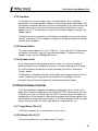
3.4 Device Control
Figure 8 : Device Control Panel
Lists information about the selected target and allows the
user to edit the communication bit rate, as well as the
target's slave address, when applicable.
3.4.1 Bit Rate
The bit rate is the speed of communications between the Promira, Cheetah or Aardvark
adapter and the target memory device.
The Promira platform can operate at bit rate from 1 kHz to 1 MHz in I2C mode, and from
31 kHz to 80 MHz in SPI mode depending on licensed capability.
Cheetah adapter can operate at bit rates from 100 kHz to 40 MHz. It is also possible to
overclock the Cheetah adapter to bit rates beyond 40 MHz. The maximum settable bit
rate is 50 MHz, though this speed is beyond advised specifications.
The Aardvark adapter can operate at bit rates from 1 kHz to 800 kHz in I2C mode, and
from 125 kHz to 8 MHz in SPI mode.
Changing the Bit Rate
The most commonly used bit rates are automatically provided in the bit rate drop-down
menu. To change the bit rate, simply select a bit rate from the drop-down menu.
Alternatively, it is also possible to enter any arbitrary bit rate greater than 32 kHz. Only
integer values are accepted; decimal bit rate values (e.g., 1.3 MHz) will cause an error
message to be displayed. Bit rates can be specified in either kilohertz (kHz) or
megahertz (MHz). If no units are specified, it will be assumed that the bit rate is being set
in kilohertz.
21
Flash Center User Manual v1.43
Once a bit rate is entered, the accept (check) and cancel (X) icons next to the bit rate
box will become active. Conversely, many other controls in the software will become
disabled until the new bit rate is either accepted or canceled. To accept the bit rate that
has been entered, simply click on the green check mark. To cancel the data entry,
simply click on the red "X". When a data entry has been canceled, the previous bit rate
setting will be restored.
When the accept button is clicked, the software will attempt to set the bit rate for all
connected adapters. If the requested bit rate is not available, the closest available bit
rate will be set. In such a case, a warning message will be inserted in the transaction log
to inform the user of the actual bit rate set. The bit rate must be within both the maximum
bit rate for the selected memory device, as well as the maximum bit rate supported by
each programming adapter.
If the bit rate has been successfully set, a message will appear in the transaction log
indicating the bit rate change.
3.4.2 I2C Slave Address
If the target memory device communicates over the I2C bus, and the Flash Center is
connected to one or more Promira platform or Aardvark adapters, the I2C Slave Address
text box becomes active. When the flash device is selected, the I2C Slave Address will
be set to the default address, which is the address the device will respond to if all of the
address lines are tied to ground (logic 0).
To change the slave address, type the new address in the textbox and press the "Enter"
key. The address can be entered in decimal, octal with a leading 0 (e.g., 0100 ) or
hexadecimal with a leading 0x (e.g., 0x50 ). To cancel a slave address entry press the
"ESC" key.
For certain I2C devices, when the capacity of the device exceeds the total number of bits
supplied in its address word, the device will use the lower bits of the I2C device address
to fully address the data (e.g., 0x52 and 0x53 would be reserved for a device that has a
capacity of 512 bytes and only an 8-bit address word specification, when the custom
address is set to 0x52 ). The Flash Center recognizes this automatically and reserves
those extra I2C device addresses. The user is not allowed to enter in addresses that
impinge on this requirement.
3.4.3 SPI I/O Mode
Some memory devices support dual I/O or quad I/O mode to pass data in or out faster.
The Promira platform SPI supports dual and quad SPI depending on licensed
application.
If the target memory device, included in the Flash Center's parts list, supports dual or
quad SPI, it will show up in SPI I/O Mode combo box. If the adapter doesn't support dual
or quad SPI mode, the operation will be run in single SPI mode.
22
Flash Center User Manual v1.43
Most of SPI transaction consists of three parts: command, address and data. Command
is always transmitted in standard SPI, however the SPI modes for address and data can
be configurable. See Section 4 for more information how to configure dual/quad SPI
mode.
3.5 Data
The Data panel contains the data that will be written to a device at the next programming
operation. The data can be read from a file or manually entered by the user.
Figure 9 : Data Panel
Displays data read from the memory device or from a file.
Allows the user to manipulate the data to be programmed to
the memory device.
3.5.1 Hex Editor
The Data panel includes a full-featured hex editor. The data can be specified in either
hexadecimal or ASCII. The left side of the hex editor is the address offset of the data
row. The middle section is the data represented in hexadecimal format. The right side is
the data represented in ASCII format.
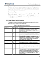
There are several keyboard shortcuts available while working in the hex editor.
Table 1 : Hex Editor Keyboard Shortcuts
23
Flash Center User Manual v1.43
Key(s)
Function
Arrow keys
Move one space left, right, up or down
Home
Move to the beginning of the row
End
Move to the end of the row
Page Up
Move one screen up
Page Down
Move one screen down
Ctrl-Home
Move to the beginning of the message
Ctrl-End
Move to the end of the message
Shift
When holding it down, selects the text under the cursor. This can be used in
conjunction with the movement keys above and the mouse.
Ctrl-A
Selects all data in the hex editor
Ctrl-Tab
Switches between Hex and ASCII mode (Linux only)
Ctrl-Left
Switches to Hex mode
Ctrl-Right
Switches to ASCII mode
Insert
Toggles between Insert mode and Overwrite mode
Ctrl-Delete
Shift-Delete
Ctrl-X
Cut
Ctrl-Insert
Ctrl-C
Copy
Ctrl-V
Paste
When moving around in the Hex Editor, the current location in the current mode (Hex or
ASCII) is marked with the cursor. The equivalent position in the other mode is marked by
green text. If the Hex Editor is in Insert mode, the cursor will be a line. If the Hex Editor is
in Overwrite mode, the cursor will be a box.
The entire data buffer can be immediately cleared by clicking on the "Clear" button.
3.5.2 Fill
A specified number of bytes can be placed at the current cursor position by clicking the
"Fill" button. When the button is clicked, a dialog box will appear where the number of
bytes can be specified. The value of the bytes added is defined by a pattern of one or
more bytes. The fill pattern can be specified in the Pad text box. There must be at least
one byte of padding defined in the Pad field before clicking the "Fill" button.
When the "OK" button is pressed, the selected number of padding bytes will be added
to Hex Editor at the cursor location. The fill pattern bytes will be repeated until the
24
Flash Center User Manual v1.43
specified number of bytes has been inserted. If the Hex Editor is in Overwrite mode, then
the bytes added will overwrite existing data.
Figure 10 : Fill Dialog
The number of padding bytes to be inserted at the current
cursor position can be specified in this dialog window.
3.5.3 Pad
A string of up to 16 hexadecimal byte values can be specified in this text box. The byte
sequence specified is used as the fill pattern when using the Fill option as well as for
filling undefined regions when loading Hex or S-Record files.
The format of the pad value should be two hexadecimal digits for each byte of the
pattern with each byte separated by a single space.
3.5.4 Load File
The contents of a binary, Intel Hex, or Motorola S-Record file can be read into the Data
buffer. Clicking the "Load File" button will cause a file dialog to open and the user to
select the file.
When loading an Hex or S-Record file, any undefined regions in the file will be filled with
the byte sequence specified in the Pad text box. The data pattern will be repeated
through all undefined regions of memory in the data image, aligned to the data pattern
size.
There must be at least one byte of padding defined in the Pad field before loading a file.
3.5.5 Save File
The entire data buffer can also be saved to a binary, Intel Hex, or Motorola S-Record file
by clicking on the "Save File" button. When the button is clicked, a file dialog window
will appear to allow a file to be created with the contents of the data buffer.
25
Flash Center User Manual v1.43
3.6 Memory Operations
All of the memory operations are found in the toolbar (or through the menubar). Memory
operations are multi-threaded, that is, an operation in progress on one device is
independent of a simultaneous operation on another device.
Figure 11 : Operation in Progress
The large status bar at the top shows total progress, and
the smaller status bars show the progress for each adapter.
All operations update the progress bar, so it is easy to tell at a glance how much time is
remaining. There is a progress bar associated with each device and a main status bar
which shows aggregate status (Figure 11). The main status bar will reflect the status of
the slowest adapter.
26
Flash Center User Manual v1.43
If there are errors during a given memory operation, the status will appear in the
transaction log immediately and error dialogs will be displayed after all adapters have
completed their respective operations. An operation in progress can be interrupted by
clicking the "Abort" button, or pressing Ctrl-Z.
3.6.1 Read Device
If a target device has been selected and adapters are connected, the "Read Device"
toolbar button becomes available. When the button is clicked, the contents of the
selected device are read and will replace the current contents in the data buffer. If
multiple devices are selected, a dialog will pop up in which the user can specify which
device should be used to perform the read.
Figure 12 : Read Selection Dialog
Allows the user to select the adapter from which to read
when multiple adapters have been enabled prior to device
read operation.
3.6.2 Program + Verify
The Program + Verify cycle writes data to one or more attached memory devices and
then reads back the data to verify it for correctness. If any part of the sequence fails, a
status message will be placed in the transaction log immediately and an error dialog will
be subsequently displayed after all adapters have finished their operations.
27
Flash Center User Manual v1.43
The Program + Verify cycle can be selected by clicking the toolbar icon, selecting
Operations | Program + Verify from the menu, or pressing the shortcut sequence Ctrl
+P.
If the device is an SPI Flash, an erase cycle will be performed first. The erase will cover
only those sectors which will be written. Note that it is possible to erase more data than
is written, if a write ends in the middle of a sector. A warning will be logged if this is the
case. Also, if the data to be written is large enough to require the entire device to be
erase, and the memory device has an erase all instruction, the software will use the
"erase all" instruction. In this case, the progress bar will only be an estimate of how long
the erase is taking. The entire device will be erased even if the operation is aborted in
mid-course.
Programming a device requires that the Flash Center is connected to at least one
adapter, a flash device has been selected, and there is data in the data buffer. One or
more devices must be selected by checking the associated checkbox.
3.6.3 Program
The Program cycle writes data to the device, but does not perform the verification step.
Requirements are the same as for Program + Verify.
If the device is an SPI Flash, an erase cycle will be performed first, with the same
caveats as Program + Verify.
The Program cycle can be selected by clicking the Program button in the Operations
section, selecting Operations | Program from the menu, or pressing the shortcut
sequence Ctrl+G.
3.6.4 Program (No Erase)
The Program (No Erase) cycle is a special mode for SPI Flash devices. It writes data to
the device, but does not perform an erase cycle. This is useful if multiple memory
images are to be programmed to the device. (Use FF as the pad value when loading
each memory image to avoid corrupting previously written data.)
Because the device may have been programmed prior to this operation, it does not
perform the verification step. Requirements are the same as for Program + Verify.
The Program cycle can be selected by clicking the Program button in the Operations
section, selecting Operations | Program (No Erase) from the menu, or pressing the
shortcut sequence Ctrl+M.
3.6.5 Verify
This verifies the contents of the selected devices against the contents of the data buffer.
28
Flash Center User Manual v1.43
The Verify cycle can be selected by clicking the Verify button in the Operations section,
selecting Operations | Verify from the menu, or pressing the shortcut sequence Ctrl+Y.
3.6.6 Erase
Figure 13 : Erase Parameters
Allows the user to erase the entire device, or specify a start
address and length to erase only a portion of the device.
The erase cycle allows the user to erase the entire memory device or allows the erasure
of portion of it. For partial erasure, users can specify the start addresses and length in
the erase parameters dialog (Figure 13 ) as either a decimal value or as a hexadecimal
value with the "0x" prefix.
If a device does not have an erase instruction, zeros are written to the specified range
within the device. Otherwise, check the memory device manual for erase behavior.
The Erase cycle can be selected by clicking the Erase button in the Operations section,
selecting Operations | Erase from the menu, or pressing the shortcut sequence Ctrl+E.
The erase cycle can be selected even if there is no data in the Hex Editor.
Note: For flash devices, it is possible for the erase range to be expanded in the situation
where the address range starts in the middle of a sector and/or ends in the middle of a
sector. Flash devices can only be erased in sector increments. A warning will be logged
if the address range is expanded to satisfy sector boundaries.
Note: If the specified length for the erase operation encompasses the entire device size,
and the memory device has an "erase all" instruction, the software will use this
"erase all" instruction. In this case, the progress bar will only be an estimate of how long
29
Flash Center User Manual v1.43
the erase is taking. The entire device will be erased even if the operation is aborted in
mid-course.
3.7 Transaction Log
The Transaction Log provides a history of all of the operations performed by the Flash
Center.
Figure 14 : Transaction Log
Records all transactions that are performed by the Flash
Center. This log can be saved as a file for future reference.
The information is arranged in the following columns:
Severity: An indication of the severity of the message. Warnings will be flagged with a
small yellow triangle with an exclamation point, and errors will be flagged with a red stop
sign.
Index: Index number of the transaction. The index is a zero-based number.
Timestamp: Time of the transaction. This information is displayed in the format:
YYYY-MMM-DD hh:mm:ss.xxx
Summary: A summary of the operation performed. Messages that are associated with
specific devices will start with "Adapter(s) 1,2:" followed by the message, where the
30
Flash Center User Manual v1.43
numbers indicate which adapters the message is associated with. Messages that do not
start with adapter numbers are assumed to have global scope.
3.7.1 Clear
The "Clear" button immediately clears all entries from the Transaction Log.
3.7.2 Save Log
The data in the log can be exported in a comma-separated values (CSV) format by
clicking on the "Save..." button. You will be prompted for a filename to save the data.
The log file has a header with the following information:
Export Time: [time of export]
After the header, all transactions are appended, one per line. The column order in the
exported file is the same as the order of the columns in the transaction log.
31
Flash Center User Manual v1.43
4 Adding Memory Devices
4.1 Introduction
While there are many memory devices included in the Flash Center's parts list by
default, users may find that the part that they wish to program is not present. Hence, the
Flash Center includes a method to allow users to add additional memory parts to the
library and to specify the parameters for programming these parts. In order to add a
memory device to the Flash Center, the user must first define the memory parts
programming parameters in an XML file and then load the file into Flash Center.
4.2 Importing Memory Device Files
There are two ways to add memory devices into the Flash Center's parts list from a
memory part file.
One method for loading the file in the Flash Center is to open the "Select Target Device"
dialog and then click the "Load Part File..." button. The memory part file can be then
chosen from the file selection dialog.
The other way to add the parts defined in a memory part file is to put the file into the
Flash Center's parts directory. This directory is located in the Flash Center's installation
directory and is named parts. When the Flash Center is launched, it will automatically
load all files in the parts directory that have the .xml file extension.
Regardless of the method chosen to load the memory part file, if the file is properly
formatted, the parts will be integrated into the parts list and can be selected for
programming in the Choose Target Device dialog.
Note: The deviceName parameters for the memory devices must be unique. If there is a
duplication of the deviceName parameters between parts definitions, then parts loaded
later will overwrite parts definitions loaded earlier. When using the "Load Part File..."
option, this is useful as it allows for the refinement of parts definitions without having to
restart Flash Center. When the parts with duplicate deviceName parameters are located
in the parts directory, it is indeterminate which one will be loaded.
4.3 Defining Memory Device Files
In order to add a memory device to the Flash Centers parts list, the part must first be
defined in a memory part file.
32
Flash Center User Manual v1.43
In order to use higher bitrate than the maximum bitrate specified in parts library with the
Promira Serial Platform, a file under parts directory needs to be updated.
• The maximum SPI bitrate with the Promira Serial Platform with SPI Active Level 3
application is 80MHz.
• Check the memory part datasheet to make sure the memory part supports the
desired bitrate.
• Open the file under parts directory that specifies the desired memory part.
• Update maxBitrate to the desired bitrate. Make sure this bitrate is equal to or
below the maximum bitrate for your Promira Serial Platform.
• Not recommended to update other nodes.
The following is an example of a memory part file, taken from one of the files that ships
with the Flash Center, st-spi-flash-m25pe.xml. It defines 4 memory parts which
inherit the bulk of their parameters from the global default values or the default values
declared at the top of the file.
<?xml version="1.0" encoding="UTF-8"?>
<devices>
<default version="1.0">
<manufacturerName> STMicro </manufacturerName>
<deviceAlgorithm>SPI flash</deviceAlgorithm>
<maxBitrate>33000</maxBitrate>
<addressWidth>3</addressWidth>
<readDummyBytes>1</readDummyBytes>
<writeSize>256</writeSize>
<eraseSize>256</eraseSize>
<writeTime>1200</writeTime>
<eraseTime>10000</eraseTime>
<readInstruction>0x0b</readInstruction>
<readDeviceIdInstruction>0x9f</readDeviceIdInstruction>
<eraseInstruction>0xdb</eraseInstruction>
<deviceConnectedBits>0x00</deviceConnectedBits>
<deviceConnectedMask>0xfc</deviceConnectedMask>
</default>
<device version="1.0">
<deviceName>M25PE10</deviceName>
<deviceDescription>
STMicro M25PE10 128 Kilobyte SPI Flash
</deviceDescription>
<capacity>128*1024</capacity>
<expectedDeviceId>\\x20\\x80\\x11</expectedDeviceId>
</device>
<device version="1.0">
<deviceName>M25PE20</deviceName>
<deviceDescription>
STMicro M25PE20 256 Kilobyte SPI Flash
</deviceDescription>
<capacity>256*1024</capacity>
<expectedDeviceId>\\x20\\x80\\x12</expectedDeviceId>
33
Flash Center User Manual v1.43
</device>
<device version="1.0">
<deviceName>M25PE40</deviceName>
<deviceDescription>
STMicro M25PE40 512 Kilobyte SPI Flash
</deviceDescription>
<capacity>512*1024</capacity>
<expectedDeviceId>\\x20\\x80\\x13</expectedDeviceId>
</device>
<device version="1.0">
<deviceName>M25PE80</deviceName>
<deviceDescription>
STMicro M25PE80 1 Megabyte SPI Flash
</deviceDescription>
<capacity>1024*1024</capacity>
<maxBitrate>50000</maxBitrate>
<hasEraseAll>true</hasEraseAll>
<writeTime>1350</writeTime>
<eraseAllTime>10*1000000</eraseAllTime>
<eraseAllInstruction>0xc7</eraseAllInstruction>
<expectedDeviceId>\\x20\\x80\\x14</expectedDeviceId>
</device>
<device version="1.0">
<deviceName>M25PE16</deviceName>
<deviceDescription>
STMicro M25PE16 2 Megabyte SPI Flash
</deviceDescription>
<capacity>2*1024*1024</capacity>
<maxBitrate>50*1000</maxBitrate>
<blockProtectBits>0x1c</blockProtectBits>
<hasEraseAll>true</hasEraseAll>
<writeTime>800</writeTime>
<eraseAllTime>17*1000000</eraseAllTime>
<eraseAllInstruction>0xc7</eraseAllInstruction>
<expectedDeviceId>\\x20\\x80\\x15</expectedDeviceId>
<deviceConnectedMask>0x60</deviceConnectedMask>
</device>
</devices>
4.3.1 Memory File Part Format
The parts definition format used for the Flash Center is based upon XML. (For an
overview of the XML format, please refer to the official XML website at http://
www.w3.org/XML/ ).
The memory part file format contains multiple elements. It begins with the XML
declaration and is followed by the <devices> node which can contain one <default>
node and multiple <device> nodes. The <default> node and the <device> nodes
each contain multiple elements which define parameter values for memory devices.
Each <device> node defines a single memory device. The <default> node can be
used to define common features of all of the memory parts in the file.
XML Declaration
34
Flash Center User Manual v1.43
The first line in the example file is the XML declaration line. This line should be the first
line in all memory part files.
Devices Node
The only item at root level in the XML file is the <devices> element node. All other
elements in the file are subnodes of the <devices> node; the second line of the file
should be the declaration of the <devices> node and the last line of the file should
close the <devices> node. The <default> node and all of the <device> nodes
should be subnodes of the <devices> node.
Default Node
The <default> node is an optional node that defines the shared parameter values for
all the devices defined in the file. Any parameters defined in the <default> node will
override the built-in default values for that individual parameter.
The <default> element has one attribute, version, which must be set to 1.0. There
should be only one <default> node. If there is more than one <default> node, only
the first one is parsed; the rest are ignored.
Device Nodes
Each <device> node in the memory part file defines a single memory part. Multiple
<device> nodes are allowed under the <devices> node, each one defining a different
memory device. The parameter values declared under each <device> node define the
features of the device and also characterize the programming methodology for the
memory device. The parameters defined within each <device> node will vary
depending on the type of memory device plus the specifics of the memory device.
It is important when adding new parts into the Flash Center's part list that the new part
has a unique name, as defined in the <deviceName> parameter. If there are memory
parts that have the same <deviceName> value, only one of the parts will be included in
the parts list. In this situation, a warning will be displayed to the user.
The <device> element has one attribute, version, which must be set to 1.0.
DualIO Node and QuadIO Node
The <dualIO> node and the <quadIO> node, that are allowed under the <device>
node, are to define dual I/O and quad I/O mode for the memory device. When dual or
quad is selected for SPI I/O Mode, the parameters under the <dualIO> or <quadIO>
35
Flash Center User Manual v1.43
node will be used. Any parameters not defined under these nodes will be inherited from
the <device> node
4.3.2 Device Parameters
In the memory parts file, each memory device is described as a list of parameter values
which define features such as the name of the device, the size of the memory, the type
of device, etc. The parameters required to define a particular memory part will vary
depending on what type of memory device it is as well as other specific features of the
part.
Note: Parameter names are case-sensitive.
Default parameter values
Some parameters have default values defined, so they need not be defined for most
memory devices. For example, baseDeviceAddress and writeInstruction have
default values of 0x50 and 0x02, respectively. These default values are taken from
typical values for these parameters. For many memory parts, the default values will be
correct, so these parameters need not be defined in the <device> node. For those
parts whose parameter values differ from the default values, specifying that parameter
will override the default value.
Additionally, it is possible to define file-specific default parameter values by defining the
parameter value in the <default> node. The parameters defined under the
<default> node will override the regular default values. As with the normal default
values, the file-specific defaults can also be overridden in the <device> node for any
individual memory part.
Parameter Types
There are four main types of device parameters: text, boolean, integer, and binary data.
In addition, there is one parameter, deviceAlgorithm, that is a text type parameter for
which only three specific values are accepted.
The "text" parameters can accept any text input. Examples include manufacturerName
and deviceDescription, where any XML-permitted string value is allowed.
The "boolean" parameters allow two values: true or false, case insensitive. Examples
of boolean parameters are hasEraseAll and busyBitPolarity.
The "integer" parameters take unsigned numeric values. By default, integer values will
be parsed as decimal values. Prefixing the value with 0x will cause the Flash Center to
parse the value as a hexadecimal value. In addition, integer values can be defined as
the multiplication of two values, using the * symbol. (Space characters are not allowed
around the * symbol.) For example, 16384, 0x4000, 16*1024, 0x10*0x400, and
0x10*1024 all represent the same value. Examples of integer parameters are
capacity, writeInstruction, and deviceBusyBit.
36
Flash Center User Manual v1.43
The "binary data" parameters represent a sequence of byte values. Each byte value in
the sequence can be represented by any XML-permitted character or can be entered as
a hexadecimal value prefixed with \x. For example, abc123, \x20\x80\x14, and abc
\xff are all valid entries for a binary data value.
Memory Device Types
There are three types of memory devices supported by the Flash Center. These are: I2C
EEPROM, SPI EEPROM, and SPI flash. Some memory device parameters are common
to all three memory device types, while some are specific to I2C EEPROMs, some are
specific to SPI devices (both EEPROMs and flash devices), and some parameters are
specific to SPI flash devices.
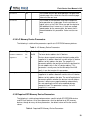
4.3.3 Global Memory Device Parameters
The following is a table of the parameters common to all memory devices. All of these
parameters must be defined for every memory part.
Table 2 : Global Memory Device Parameters
Parameter
Type
Default
deviceAlgorithm
text
The type of memory device. The programming algorithm
will be determined based on this parameter value.
Supported values are i2c eeprom, spi eeprom, and spi
flash, case insensitive.
deviceName
text
The name of the memory device. Note that the device
name must be unique; devices with duplicate names will
result in an error.
deviceDescription
text
A long description of the device. Displayed when the
memory device is selected during selection of the target.
Typically, it contains the manufacturer name, device
name, memory size, and device type.
manufacturerName
text
The manufacturer of the memory device.
capacity
int
Size of the device in bytes. Value must be non-zero.
maxBitrate
int
The maximum bit rate the device can use to
communicate to the programming adapter. Value must
be non-zero. If there are multiple speed grades for the
memory part, the highest bit rate is recommended for
this parameter.
addressWidth
int
1
Description
The number of bytes in the memory address field when
reading from and writing to the device. If the address
has overflow bits they will automatically be added to the
device address (I2C) or command code (SPI). Value
must be non-zero.
37
Flash Center User Manual v1.43
writeSize
int
The number of bytes per write operation. For parts with
variable page sizes, enter the size of the smallest page.
Value must be non-zero.
writeTime
int
The number of microseconds required to complete a
write operation to a single page. Use the minimum or
typical value, as the Flash Center can poll the device to
wait additional time if necessary. If there are multiple
speed grades for the memory part, the lowest time is
recommended for this parameter. Value must be nonzero.
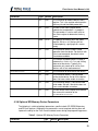
4.3.4 I2C Memory Device Parameters
The following is a table of the parameters specific to I2C EEPROM memory devices.
Table 3 : I2C Memory Device Parameters
Parameter
Type
Default
Description
baseDeviceAddress
int
0x50
The base device address for I2C devices.
pageShift
int
0
Devices whose capacity exceeds the total number of bits
supplied in its address word, will use bits of the I2C device
address to fully address the data. The pageShift
parameter specifies the position of the least significant bit
of such address bits in the I2C device address. This
parameter is usually zero, but the Microchip 24xx1025
family is one that requires this parameter.
autoPageUpdate
bool
true
Devices whose capacity exceeds the total number of bits
supplied in its address word will use bits of the I2C device
address to fully address the data. The autoPageUpdate
parameter specifies whether the devices internal address
counter is able to cross page boundaries automatically,
thus not requiring these bits to be modified during a
sequential read. This parameter is always false if
pageShift is not zero.
4.3.5 Required SPI Memory Device Parameters
The following is a table of required parameters specific to both SPI EEPROM devices
and SPI flash devices. All of these parameters must be defined for all SPI memory
devices, though for many of these parameters, the default values will be the correct
values.
Table 4 : Required SPI Memory Device Parameters
38
Flash Center User Manual v1.43
Parameter
Type
Default
Description
readStatusRegisterInstruction
int
0x05
The instruction to read the device status
register. This is the register which contains
the busy bit and the block protect bits.
deviceBusyBit
int
0x01
The bits in the status register which
indicate that an operation is in progress.
This parameter is used as a bit mask on
the status register to determine the busy
status.
busyBitPolarity
bool
false
The polarity of the busy bit in the status
register. Set to true if the busy bit has
inverted polarity, signifying that 1 means
ready.
readInstruction
int
0x03
The instruction which initiates a read
operation from the device. For devices with
a fast read command, the default value
should be overridden.
readDummyBytes
int
0
The number of padding bytes inserted in
between the readInstruction and shifting
data out of the device. Typically, this
parameter only needs to be set for flash
devices with a fast read command.
writeInstruction
int
0x02
The instruction to write data to the device.
writeEnableInstruction
int
0x06
The instruction which is sent to enable
writing to the device. Set to 0 if the device
does not have a write enable instruction.
writeDisableInstruction
int
0x04
The instruction which is sent to terminate
write mode. Set to 0 if the device does not
have a write disable instruction.
writeEnableBits
int
0x02
The bits of the status register that indicate
the successful execution of the
writeEnableInstruction.
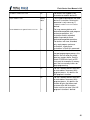
4.3.6 Optional SPI Memory Device Parameters
The following is a table of optional parameters specific to both SPI EEPROM devices
and SPI flash devices. Although these parameters are not required, defining them will
improve the ability for the Flash Center to detect errors during the programming process.
Table 5 : Optional SPI Memory Device Parameters
Parameter
Type
Default Description
39
Flash Center User Manual v1.43
readDeviceIdInstruction
int
For devices that support it, the
instruction to read the device ID.
expectedDeviceId
binary
data
The ID code expected from the read
device ID instruction. Defining this
parameter is only necessary if
readDeviceIdInstruction is also
defined.
extendedAddressingEnableInstruction
int
For large memory devices with
backward compatible read, program
and erase operations, this
instruction enables extended
addressing mode for those
backward compatible operations.
For devices with new, extendedonly read, program and erase
instructions, supply those
instructions in lieu of this command.
writeBufferInstruction
int
For memory devices that have a
two-part page program process, this
defines the instruction for writing
data to a memory buffer. See the
Atmel AT45DBxxxx family of SPI
flash parts for examples of memory
parts that use memory buffers for
page programming.
writeAutoAddressIncrementInstruction
int
For SST memory devices that have
an auto address increment (AAI)
program process, this defines the
AAI program instruction.
writeAutoAddressIncrementSize
int
For SST memory devices that have
an auto address increment (AAI)
program process, this defines the
number of bytes that follow each
instance of the AAI instruction.
Value must be non-zero if the AAI
program instruction is defined.
40
Flash Center User Manual v1.43
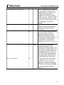
writeAutoAddressIncrementTime
int
writeStatusRegisterInstruction
int
writeStatusRegisterEnableInstruction
int
writeStatusRegisterTime
int
deviceConnectedBits
int
For SST memory devices that have
an auto address increment (AAI)
program process, this defines the
number of microseconds to
complete each AAI write iteration.
Unlike writeTime , this value should
be the maximum write time, not the
minimum. Value must be non-zero if
the AAI program instruction is
defined.
0x01
The instruction to write to the status
register. Set to 0 if the device does
not have a write status register
instruction.
The instruction to enable writing to
the status register. Define this
parameter for parts that have
separate write enable and write
status register enable instructions. If
this parameter is undefined, the
Flash Center will use the value
defined for writeEnableInstruction
.
5000
The number of microseconds
required to complete a write
operation to the status register. Use
the minimum or typical value, as the
Flash Center can poll the device to
wait additional time if necessary. If
there are multiple speed grades for
the memory part, the lowest time is
recommended for this parameter.
The bits of the status register that
are always set to 1. This is used
with the deviceConnectedMask
parameter for detecting unplugged
SPI devices. See the section below
for more information about this
parameter.
41
Flash Center User Manual v1.43
deviceConnectedMask
int
blockProtectBits
int
0x9c
Sets which bits of the status register
indicate that the device blocks or
the status register are write
protected. See the section below for
more information about this
parameter.
spiMode
int
0
Sets SPI mode (0-3).
0: Mode 0. Data are captured on the
clock's rising edge (low to high
transition) and data is propagated
on a falling edge (high to low clock
transition).
1: Mode 1. Data are captured on the
clock's falling edge and data is
propagated on a rising edge.
2: Mode 2. Data are captured on
clock's falling edge and data is
propagated on a rising edge.
3: Mode 3. Data are captured on
clock's rising edge and data is
propagated on a falling edge.
spiBitorder
bool
true
Sets SPI bitorder. The bitorder
option is used to indicate whether
LSB or MSB is shifted first. Sets
true for MSB.
spiSSPolarity
bool
true
Sets SS polarity which is the output
polarity on the SS line. Sets true for
active low.
The bits of the status register that
have a fixed value. This is used with
the deviceConnectedBits parameter
for detecting unplugged SPI
devices. If undefined, the value from
deviceConnectedBits will be used.
See the section below for more
information about this parameter.
Device Connected Bits and Mask
In the SPI protocol, there is no predefined method for an SPI slave device to
acknowledge receipt of commands from the SPI master. Therefore, the SPI master could
send the slave a command but the master may not have a method for determining if a
slave device was connected to receive it. However, if a SPI memory device has bits in
the status register that always have a fixed value, the status register can be used by
Flash Center to determine whether there is a connection to the device or not.
42
Flash Center User Manual v1.43
The deviceConnectedBits and deviceConnectedMask parameters are used to
define these bits in the status register. The deviceConnectedMask parameter tells
Flash Center which bits have a fixed value and deviceConnectedBits tells it what the
value of those bits are. If these parameters are defined for a memory device, Flash
Center will check these bits for a connection to the target device, both while the memory
device is idle and while a memory operation, such as a page program or sector erase
operation, is in progress.
If deviceConnectedBits is defined but deviceConnectedMask is undefined or 0,
Flash Center will use the value of deviceConnectedBits for
deviceConnectedMask. This results in Flash Center being only able to detect bits in
the status register that have a fixed value of 1 but not bits that have a fixed value of 0.
If both deviceConnectedBits and deviceConnectedMask are undefined or 0, then
the status register will not be used for detecting a connection to the target memory
device.
Note: Some memory devices will return different results when the status register is read
during a memory operation. For example, the Atmel AT25xxxx family will return
b1111_1111 while a memory operation is in progress. Because none of the bits in the
status register have the same value while the parts are idle, deviceConnectedBits
and deviceConnectedMask are not defined for these parts, and the status register is
not used to determine a connection to the parts.
Block Protect Bits
Most SPI memory parts have a system by which portions of the memory can be
protected from modification. The blockProtectBits parameter tells Flash Center
which bits of the status register indicate that block protection is enabled. Typically, a
memory device will have a bit in the status register to indicate that block protection is
enabled as well as bits used to indicate which blocks are protected. All of these bits
should be included in the blockProtectBits parameter.
At the beginning of an erase or a write operation, if any of the block protect bits in the
status register are non-zero, the Flash Center will write 0 to the status register in an
attempt to clear the block protection. If the write status register instruction is not defined
or writing to the status register fails to clear the block protect bits, an error message will
be displayed and the operation will exit.
For devices whose block protect bits are not cleared by writing to the status register (e.g.
they have special instructions to clear the block protection), the block protection will have
to be cleared prior to using Flash Center to program the device.
4.3.7 User-Definable SPI Memory Device Parameters
The following is a table of optional, user-definable parameters available for both SPI
EEPROM devices and SPI flash devices. Two user transaction fields allow users to
43
Flash Center User Manual v1.43
define arbitrary SPI transaction data that Flash Center will send before each read, write,
and erase operation.
Table 6 : User-Definable SPI Memory Device Parameters
Parameter
Type
Default
userTransaction1
binary
data
User-definable transaction sent before the
start of each read, program, or erase
operation.
userTransaction2
binary
data
User-definable transaction sent before the
start of each read, program, or erase
operation.
userTransaction1WriteEnable
bool
false
Description
Set to true to send the
writeEnableInstruction
before sending
userTransaction1.
userTransaction2WriteEnable
bool
false
Set to true to send the
writeEnableInstruction
before sending
userTransaction2.
userTransaction1Time
int
The number of microseconds required to
complete userTransaction1. Use the
minimum or typical value, as the Flash
Center can poll the device to wait additional
time if necessary. If there are multiple speed
grades for the memory part, the lowest time
is recommended for this parameter.
userTransaction2Time
int
The number of microseconds required to
complete userTransaction2. Use the
minimum or typical value, as the Flash
Center can poll the device to wait additional
time if necessary. If there are multiple speed
grades for the memory part, the lowest time
is recommended for this parameter.
Notes on User-Definable Transactions
The bytes supplied in the two userTransaction fields are sent as-is on the SPI bus.
The instruction byte and other data should be combined in one userTransaction
field. If the operation provided requires write enable (e.g. register programming), use the
write enable bool fields.
The following example demonstrates programming a non-volatile configuration register
with instruction 0xB1, data 0xFFFF, WREN required, and average commit time
0.2 seconds.
44
Flash Center User Manual v1.43
<userTransaction1>\\xB1\\xFF\\xFF</userTransaction1>
<userTransaction1WriteEnable>true</userTransaction1WriteEnable>
<userTransaction1Time>200000</userTransaction1Time>
4.3.8 SPI Flash Memory Device Parameters
The following is a table of the parameters specific to SPI flash memory devices.
Table 7 : SPI Flash Memory Device Parameters
Parameter
Type
Default
eraseInstruction
int
The instruction which erases a portion of the device. If
the device has multiple erase sizes (for devices with
both sector and block erase), it is recommended that
the instruction for the smaller erase size be given.
eraseSize
int
The size in bytes of the portion erased by
eraseInstruction . If the device has multiple erase
sizes (for devices with both sector erase and block
erase), it is recommended that the smaller size be
specified. Value must be non-zero.
eraseTime
int
The number of microseconds required complete the
erase operation specified in eraseInstruction . Use
the minimum or typical value, as the Flash Center can
poll the device to wait additional time if necessary. If
there are multiple speed grades for the memory part,
the lowest time is recommended for this parameter.
Value must be non-zero.
hasEraseAll
bool
eraseAllInstruction
int
The instruction to execute a full chip erase.
eraseAllTime
int
The number of microseconds required to execute the
chip erase operation. Use the minimum or typical value,
as the Flash Center can poll the device to wait
additional time if necessary. If there are multiple speed
grades for the memory part, the lowest time is
recommended for this parameter. Value must be nonzero.
eraseBeforeWrite
bool
false
true
Description
If set to true, indicates that the device has support for
the chip erase command and eraseAllInstruction
and eraseAllTime must be defined.
If set to false, Flash Center will not issue erase
commands before a write command. This is useful for
devices such as the Atmel AT45DBxxxx family of SPI
flash parts, as they support a single command that
erases and programs a page of memory.
45
Flash Center User Manual v1.43
4.3.9 SPI I/O Mode Parameters
The following is a table of the parameters specific to SPI flash memory devices.
Table 8 : Multi I/O SPI Mode Parameters
Parameter
Type
Default
Description
ioModeAddress
int
1
The SPI I/O mode used to transmit address field of
SPI transaction and possible values are 0, 2, or 4.
ioModeDataIn
int
1
The SPI I/O mode used to receive data field of SPI
transaction and possible values are 0, 2, or 4.
ioModeDataOut
int
1
The SPI I/O mode used to transmit data field of SPI
transaction and possible values are 0, 2, or 4.
46
Flash Center User Manual v1.43
5 Legal / Contact
5.1 Disclaimer
All of the software and documentation provided in this manual, is copyright Total Phase,
Inc. ("Total Phase"). License is granted to the user to freely use and distribute the
software and documentation in complete and unaltered form, provided that the purpose
is to use or evaluate Total Phase products. Distribution rights do not include public
posting or mirroring on Internet websites. Only a link to the Total Phase download area
can be provided on such public websites.
Total Phase shall in no event be liable to any party for direct, indirect, special, general,
incidental, or consequential damages arising from the use of its site, the software or
documentation downloaded from its site, or any derivative works thereof, even if Total
Phase or distributors have been advised of the possibility of such damage. The software,
its documentation, and any derivative works is provided on an "as-is" basis, and thus
comes with absolutely no warranty, either express or implied. This disclaimer includes,
but is not limited to, implied warranties of merchantability, fitness for any particular
purpose, and non-infringement. Total Phase and distributors have no obligation to
provide maintenance, support, or updates.
Information in this document is subject to change without notice and should not be
construed as a commitment by Total Phase. While the information contained herein is
believed to be accurate, Total Phase assumes no responsibility for any errors and/or
omissions that may appear in this document.
5.2 Life Support Equipment Policy
Total Phase products are not authorized for use in life support devices or systems. Life
support devices or systems include, but are not limited to, surgical implants, medical
systems, and other safety-critical systems in which failure of a Total Phase product could
cause personal injury or loss of life. Should a Total Phase product be used in such an
unauthorized manner, Buyer agrees to indemnify and hold harmless Total Phase, its
officers, employees, affiliates, and distributors from any and all claims arising from such
use, even if such claim alleges that Total Phase was negligent in the design or
manufacture of its product.
5.3 Contact Information
Total Phase can be found on the Internet at http://www.totalphase.com/. If you have
support-related questions, please submit New Request on http://www.totalphase.com/
support/. For sales inquiries, please contact [email protected].
47
Flash Center User Manual v1.43
©2014-2015 Total Phase, Inc.
All rights reserved.
48