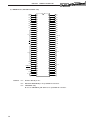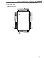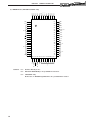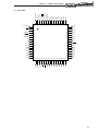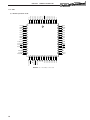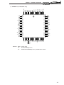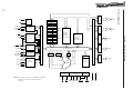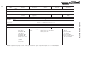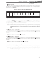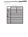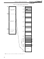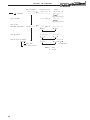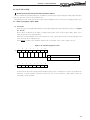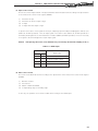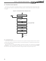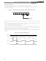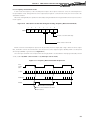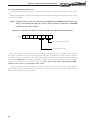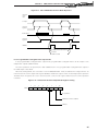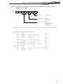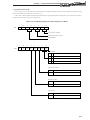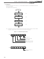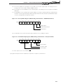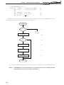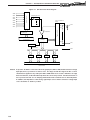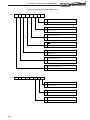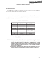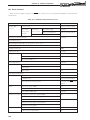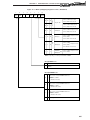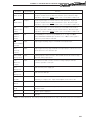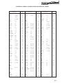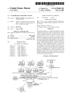
1
To our customers, Old Company Name in Catalogs and Other Documents On April 1st, 2010, NEC Electronics Corporation merged with Renesas Technology Corporation, and Renesas Electronics Corporation took over all the business of both companies. Therefore, although the old company name remains in this document, it is a valid Renesas Electronics document. We appreciate your understanding. Renesas Electronics website: http://www.renesas.com April 1st, 2010 Renesas Electronics Corporation Issued by: Renesas Electronics Corporation (http://www.renesas.com) Send any inquiries to http://www.renesas.com/inquiry. Notice 1. 2. 3. 4. 5. 6. 7. All information included in this document is current as of the date this document is issued. Such information, however, is subject to change without any prior notice. Before purchasing or using any Renesas Electronics products listed herein, please confirm the latest product information with a Renesas Electronics sales office. Also, please pay regular and careful attention to additional and different information to be disclosed by Renesas Electronics such as that disclosed through our website. Renesas Electronics does not assume any liability for infringement of patents, copyrights, or other intellectual property rights of third parties by or arising from the use of Renesas Electronics products or technical information described in this document. No license, express, implied or otherwise, is granted hereby under any patents, copyrights or other intellectual property rights of Renesas Electronics or others. You should not alter, modify, copy, or otherwise misappropriate any Renesas Electronics product, whether in whole or in part. Descriptions of circuits, software and other related information in this document are provided only to illustrate the operation of semiconductor products and application examples. You are fully responsible for the incorporation of these circuits, software, and information in the design of your equipment. Renesas Electronics assumes no responsibility for any losses incurred by you or third parties arising from the use of these circuits, software, or information. When exporting the products or technology described in this document, you should comply with the applicable export control laws and regulations and follow the procedures required by such laws and regulations. You should not use Renesas Electronics products or the technology described in this document for any purpose relating to military applications or use by the military, including but not limited to the development of weapons of mass destruction. Renesas Electronics products and technology may not be used for or incorporated into any products or systems whose manufacture, use, or sale is prohibited under any applicable domestic or foreign laws or regulations. Renesas Electronics has used reasonable care in preparing the information included in this document, but Renesas Electronics does not warrant that such information is error free. Renesas Electronics assumes no liability whatsoever for any damages incurred by you resulting from errors in or omissions from the information included herein. Renesas Electronics products are classified according to the following three quality grades: “Standard”, “High Quality”, and “Specific”. The recommended applications for each Renesas Electronics product depends on the product’s quality grade, as indicated below. You must check the quality grade of each Renesas Electronics product before using it in a particular application. You may not use any Renesas Electronics product for any application categorized as “Specific” without the prior written consent of Renesas Electronics. Further, you may not use any Renesas Electronics product for any application for which it is not intended without the prior written consent of Renesas Electronics. Renesas Electronics shall not be in any way liable for any damages or losses incurred by you or third parties arising from the use of any Renesas Electronics product for an application categorized as “Specific” or for which the product is not intended where you have failed to obtain the prior written consent of Renesas Electronics. The quality grade of each Renesas Electronics product is “Standard” unless otherwise expressly specified in a Renesas Electronics data sheets or data books, etc. “Standard”: 8. 9. 10. 11. 12. Computers; office equipment; communications equipment; test and measurement equipment; audio and visual equipment; home electronic appliances; machine tools; personal electronic equipment; and industrial robots. “High Quality”: Transportation equipment (automobiles, trains, ships, etc.); traffic control systems; anti-disaster systems; anticrime systems; safety equipment; and medical equipment not specifically designed for life support. “Specific”: Aircraft; aerospace equipment; submersible repeaters; nuclear reactor control systems; medical equipment or systems for life support (e.g. artificial life support devices or systems), surgical implantations, or healthcare intervention (e.g. excision, etc.), and any other applications or purposes that pose a direct threat to human life. You should use the Renesas Electronics products described in this document within the range specified by Renesas Electronics, especially with respect to the maximum rating, operating supply voltage range, movement power voltage range, heat radiation characteristics, installation and other product characteristics. Renesas Electronics shall have no liability for malfunctions or damages arising out of the use of Renesas Electronics products beyond such specified ranges. Although Renesas Electronics endeavors to improve the quality and reliability of its products, semiconductor products have specific characteristics such as the occurrence of failure at a certain rate and malfunctions under certain use conditions. Further, Renesas Electronics products are not subject to radiation resistance design. Please be sure to implement safety measures to guard them against the possibility of physical injury, and injury or damage caused by fire in the event of the failure of a Renesas Electronics product, such as safety design for hardware and software including but not limited to redundancy, fire control and malfunction prevention, appropriate treatment for aging degradation or any other appropriate measures. Because the evaluation of microcomputer software alone is very difficult, please evaluate the safety of the final products or system manufactured by you. Please contact a Renesas Electronics sales office for details as to environmental matters such as the environmental compatibility of each Renesas Electronics product. Please use Renesas Electronics products in compliance with all applicable laws and regulations that regulate the inclusion or use of controlled substances, including without limitation, the EU RoHS Directive. Renesas Electronics assumes no liability for damages or losses occurring as a result of your noncompliance with applicable laws and regulations. This document may not be reproduced or duplicated, in any form, in whole or in part, without prior written consent of Renesas Electronics. Please contact a Renesas Electronics sales office if you have any questions regarding the information contained in this document or Renesas Electronics products, or if you have any other inquiries. (Note 1) “Renesas Electronics” as used in this document means Renesas Electronics Corporation and also includes its majorityowned subsidiaries. (Note 2) “Renesas Electronics product(s)” means any product developed or manufactured by or for Renesas Electronics. 87AD SERIES µPD78C18 8-BIT SINGLE-CHIP MICROCONTROLLER © 1991 Document No. U10199EJ5V0UM00 (5th edition) (Previous No. IEU-1314) Date Published August 1995 P Printed in Japan NOTES FOR CMOS DEVICES 1 PRECAUTION AGAINST ESD FOR SEMICONDUCTORS Note: Strong electric field, when exposed to a MOS device, can cause destruction of the gate oxide and ultimately degrade the device operation. Steps must be taken to stop generation of static electricity as much as possible, and quickly dissipate it once, when it has occurred. Environmental control must be adequate. When it is dry, humidifier should be used. It is recommended to avoid using insulators that easily build static electricity. Semiconductor devices must be stored and transported in an anti-static container, static shielding bag or conductive material. All test and measurement tools including work bench and floor should be grounded. The operator should be grounded using wrist strap. Semiconductor devices must not be touched with bare hands. Similar precautions need to be taken for PW boards with semiconductor devices on it. 2 HANDLING OF UNUSED INPUT PINS FOR CMOS Note: No connection for CMOS device inputs can be cause of malfunction. If no connection is provided to the input pins, it is possible that an internal input level may be generated due to noise, etc., hence causing malfunction. CMOS devices behave differently than Bipolar or NMOS devices. Input levels of CMOS devices must be fixed high or low by using a pull-up or pull-down circuitry. Each unused pin should be connected to VDD or GND with a resistor, if it is considered to have a possibility of being an output pin. All handling related to the unused pins must be judged device by device and related specifications governing the devices. 3 STATUS BEFORE INITIALIZATION OF MOS DEVICES Note: Power-on does not necessarily define initial status of MOS device. Production process of MOS does not define the initial operation status of the device. Immediately after the power source is turned ON, the devices with reset function have not yet been initialized. Hence, power-on does not guarantee out-pin levels, I/O settings or contents of registers. Device is not initialized until the reset signal is received. Reset operation must be executed immediately after poweron for devices having reset function. QTOP is a trademark of NEC Corporation. MS-DOS is a trademark of Microsoft Corporation. PC/AT and PC DOS are trademarks of IBM Corporation. The export of these products from Japan is regulated by the Japanese government. The export of some or all of these products may be prohibited without governmental license. To export or re-export some or all of these products from a country other than Japan may also be prohibited without a license from that country. Please call an NEC sales representative. The customer must judge the need for license : µPD78C11, 78C11A, 78C12A, 78C14, 78C14A, 78CP14CW, 78CP14G-36, 78CP14GF-3BE, 78CP14L, 78C18, 78CP18CW, 78CP18GF-3BE, 78CP18GQ-36, 78C11(A), 78C11A(A), 78C12A(A), 78C14(A), 78CP14(A), 78C18(A), 78CP18(A) License not needed : µPD78C10, 78C10A, 78CG14, 78CP14DW, 78CP14KB, 78CP14R, 78C17, 78CP18DW, 78CP18KB, 78C10(A), 78C10A(A), 78C17(A) The information in this document is subject to change without notice. No part of this document may be copied or reproduced in any form or by any means without the prior written consent of NEC Corporation. NEC Corporation assumes no responsibility for any errors which may appear in this document. NEC Corporation does not assume any liability for infringement of patents, copyrights or other intellectual property rights of third parties by or arising from use of a device described herein or any other liability arising from use of such device. No license, either express, implied or otherwise, is granted under any patents, copyrights or other intellectual property rights of NEC Corporation or others. While NEC Corporation has been making continuous effort to enhance the reliability of its semiconductor devices, the possibility of defects cannot be eliminated entirely. To minimize risks of damage or injury to persons or property arising from a defect in an NEC semiconductor device, customer must incorporate sufficient safety measures in its design, such as redundancy, fire-containment, and anti-failure features. NEC devices are classified into the following three quality grades: “Standard“, “Special“, and “Specific“. The Specific quality grade applies only to devices developed based on a customer designated “quality assurance program“ for a specific application. The recommended applications of a device depend on its quality grade, as indicated below. Customers must check the quality grade of each device before using it in a particular application. Standard: Computers, office equipment, communications equipment, test and measurement equipment, audio and visual equipment, home electronic appliances, machine tools, personal electronic equipment and industrial robots Special: Transportation equipment (automobiles, trains, ships, etc.), traffic control systems, anti-disaster systems, anti-crime systems, safety equipment and medical equipment (not specifically designed for life support) Specific: Aircrafts, aerospace equipment, submersible repeaters, nuclear reactor control systems, life support systems or medical equipment for life support, etc. The quality grade of NEC devices in “Standard“ unless otherwise specified in NEC's Data Sheets or Data Books. If customers intend to use NEC devices for applications other than those specified for Standard quality grade, they should contact NEC Sales Representative in advance. Anti-radioactive design is not implemented in this product. M7 94.11 INTRODUCTION Intended Readership: This manual is intended for engineers who require an understanding of 87AD series products functions prior to designing an application system or an application program. The relevant products are the following 87AD series CMOS version products. • µPD78C10A, 78C11A, 78C10A(A), 78C11A(A) • µPD78C12A, 78C12A(A) • µPD78C14, 78C14A, 78CG14, 78CP14, 78C14(A), 78CP14(A) • µPD78C17, 78C18, 78CP18, 78C17(A), 78C18(A), 78CP18(A) Remark µPD78C10, 78C11, 78C10(A), 78C11(A) have been maintenance products since October 1991. Purpose: The purposes of this manual is that users understand the hardware functions of 87AD series products shown in the organization below. Organization: This manual is mainly composed of the following contents. • General description • Pin functions • Internal block functions • Interrupt control functions • External device accesses and timing • PROM accesses • Instruction set • Operating precautions Using This Information: Use of this information requires general knowledge of electricity, logic circuits and microcontrollers. This manual describes the µPD78C18 as a representative product as long as there are no differences in the functions. Using this manual as the other 87AD series (CMOS) products manual, refer to the manual by changing "µPD78C18" to each product name. For the µPD78CG14, refer to APPENDIX A INTRODUCTION TO PIGGYBACK PRODUCT. For the "Special" quality grade product, refer to the manual by changing it to the "Standard" quality grade product. ◆ For general understanding of the 87AD series (CMOS) product functions: ➡ Read in order of contents. ◆ For searching for an instruction function by mnemonics: ➡ Use APPENDIX C INDEX OF INSTRUCTIONS (ALPHABETICAL ORDER). ◆ For searching for mnemonics by the outline of functions: ➡ Search 14.6 Instruction Descriptions for the functions. Usage examples in this manual is produced for the "Standard" quality grade. Using this manual for the "Special" quality grade applications, make use of parts and circuits actually used after checking the quality grade. Operating Precaution Be sure to read CHAPTER 15 OPERATING PRECAUTIONS in which operating precautions of the 87AD series (CMOS) products are compiled. For the latest information of this products, contact our salesman or special agent. Legend: Data notation weight : Upper digits to the left, lower digits to the right Notation of active low : ××× (A line over pin or signal names) Address on the memory map : Lower address to the upper part, higher address to the lower part Note : Explanation of Note in text Caution : Content to be read carefully Remark : Complementary explanation of text Numeric notation : Binary .............. ××××B or ×××× Decimal ........... ×××× Hexadecimal ... ××××H Related Documents The following documents are provided for 87AD series CMOS version products. Numbers in the table are document numbers. Document Name Data Sheet User's Manual IC-1872 This manual Application Note Product Name µPD78C10 µPD78C11 µPD78C10A • (I) Software fundamental IC-2678 µPD78C11A IEM-1131 • (II) µPD78C12A Floating-point format µPD78C14 IC-2417 operation package µPD78C14A IC-2565 IEM-1242 µPD78CG14 IC-2564 µPD78CP14 IC-2533 Hardware µPD78C17 IC-2788 IEM-1240 µPD78C18 IC-2789 µPD78CP18 IC-3033 µPD78C10(A) IC-2814 • (III) µPD78C11(A) µPD78C10A(A) IC-2846 µPD78C11A(A) µPD78C12A(A) µPD78C14(A) IC-2813 µPD78CP14(A) IC-3068 µPD78C17(A) IC-3127 µPD78C18(A) µPD78CP18(A) IC-3233 The contents of the above documents are subject to change without prior notification. Please check whether requested documentation is the latest version. 87AD Series CMOS Version Development Expanded ROM/RAM capacity Relative performance On-chip pull-up resistor (Mask option) µ PD78C14A PROM product µ PD78C14 Expanded ROM capacity µ PD78C12A On-chip pull-up resistor (Mask option) On-chip pull-up Note resistor µ PD78C11Note (Mask option) µ PD78C10 (ROM-less product) µ PD7811H µ PD7810H (ROM-less product) µ PD78CP14 µ PD78C11A µ PD78C10A (ROM-less product) CMOS process, on-chip pull-up resistors (Mask option) Time of product release Note µPD78C10 and 78C11 are maintenance products. µ PD78C18 µ PD78CP18 (PROM product) µ PD78C17 (ROM-less product) TABLE OF CONTENTS CHAPTER 1 GENERAL DESCRIPTION ........................................................................................... 1.1 1.2 1 Features ............................................................................................................................. Ordering Information and Quality Grade ..................................................................... 3 5 1.2.1 Ordering information ........................................................................................................... 5 1.2.2 Quality grade ........................................................................................................................ 9 Pin Configurations (Top View) ....................................................................................... 10 1.3.1 Shrink DIP, QUIP (straight) (37), QUIP (36) ........................................................................ 10 1.3.2 QFP (1B/3BE), WQFN ......................................................................................................... 13 1.3.3 QFP (AB8) ............................................................................................................................ 15 1.3.4 QFJ ....................................................................................................................................... 16 Block Diagram................................................................................................................... Functional Comparison of 87AD Series CMOS Products ........................................... Differences between 87AD Series CMOS and NMOS Products ................................ Differences between "Standard" and "Special" Quality Grade Products ............... 18 19 21 22 CHAPTER 2 PIN FUNCTIONS ......................................................................................................... 23 1.3 1.4 1.5 1.6 1.7 2.1 2.2 Normal Operation Mode ................................................................................................. 23 2.1.1 PA7 to PA0 (Port A) ............................................................................................................. 23 2.1.2 PB7 to PB0 (Port B) ............................................................................................................. 23 2.1.3 PC7 to PC0 (Port C) ............................................................................................................. 23 2.1.4 PD7 to PD0 (Port D) ............................................................................................................ 25 2.1.5 PF7 to PF0 (Port F) .............................................................................................................. 26 2.1.6 WR (Write strobe) ............................................................................................................... 27 2.1.7 RD (Read strobe) ................................................................................................................. 27 2.1.8 ALE (Address latch enable) ................................................................................................. 27 2.1.9 MODE0, MODE1 (Mode) .................................................................................................... 28 2.1.10 NMI (Non maskable interrupt) ............................................................................................ 28 2.1.11 INT1 (Interrupt request) ...................................................................................................... 28 2.1.12 AN7 to AN0 (Analog input) ................................................................................................. 28 2.1.13 VAREF (Reference voltage) .................................................................................................... 28 2.1.14 AVDD (Analog VDD) ................................................................................................................ 28 2.1.15 AVSS (Analog VSS) ................................................................................................................. 29 2.1.16 STOP (Stop control input) ................................................................................................... 29 2.1.17 X1, X2 (Crystal) .................................................................................................................... 29 2.1.18 RESET (Reset) ..................................................................................................................... 29 2.1.19 VDD ........................................................................................................................................ 29 2.1.20 VSS ........................................................................................................................................ 29 2.1.21 IC .......................................................................................................................................... 29 EPROM Mode .................................................................................................................... 30 2.2.1 A14 to A0 (Address) ............................................................................................................ 30 2.2.2 O7 to O0 (Data) ................................................................................................................... 30 2.2.3 CE (Chip enable) .................................................................................................................. 30 –i– 2.2.4 OE (Output enable) ... ......................................................................................................... 30 2.2.5 MODE1, MODE0 (Mode) .................................................................................................... 30 2.2.6 RESET (Reset) ..................................................................................................................... 30 2.2.7 VPP ........................................................................................................................................ 30 2.2.8 VDD ........................................................................................................................................ 30 2.2.9 VSS ........................................................................................................................................ 30 Pin Input/Output Circuits ................................................................................................ Pin Mask Options (µPD78C18/78C14A/78C12A/78C11A Only) ................................. Processing of Unused Pins ............................................................................................. 31 37 37 CHAPTER 3 INTERNAL BLOCK FUNCTIONS ............................................................................... 39 2.3 2.4 2.5 3.1 3.2 3.3 3.4 3.5 Registers ............................................................................................................................ Mode Registers ................................................................................................................. Arithmetic Logical Unit (ALU) ........................................................................................ Program Status Word (PSW) .......................................................................................... Memory .............................................................................................................................. 39 41 42 42 44 3.5.1 µPD78C18/78C17/78C14/78C14A/78C12A/78C11A/78C10A memory configuration ...... 44 3.5.2 µPD78CP18/78CP14 memory configuration ...................................................................... 52 Timers ................................................................................................................................ Timer/Event Counter ....................................................................................................... Serial Interface .................................................................................................................. Analog/Digital Converter ................................................................................................ Interrupt Control .............................................................................................................. Zero-Cross Detector ......................................................................................................... 57 57 57 57 57 58 CHAPTER 4 PORT FUNCTIONS ..................................................................................................... 61 3.6 3.7 3.8 3.9 3.10 3.11 4.1 4.2 4.3 4.4 4.5 4.6 Port A (PA7 to PA0) ......................................................................................................... Port B (PB7 to PB0) .......................................................................................................... Port C (PC7 to PC0) .......................................................................................................... Port D (PD7 to PD0) ......................................................................................................... Port F (PF7 to PF0) ........................................................................................................... Operation of Arithmetic and Logical Operation Instruction Involving a Port and Immediate Data ................................................................................................................ 73 CHAPTER 5 TIMER FUNCTIONS .................................................................................................... 75 5.1 5.2 5.3 61 65 66 70 71 Timer Configuration ......................................................................................................... Timer Mode Register (TMM) .......................................................................................... Timer Operations ............................................................................................................. 75 77 79 CHAPTER 6 TIMER/EVENT COUNTER FUNCTIONS ................................................................... 81 6.1 6.2 Timer/Event Counter Configuration .............................................................................. Mode Registers ................................................................................................................. 81 85 6.2.1 Timer/event counter mode register (ETMM) ..................................................................... 85 6.2.2 Timer/event counter output mode register (EOM) ............................................................ 88 – ii – 6.3 Timer/Event Counter Operation .................................................................................... 90 6.3.1 Interval timer mode ............................................................................................................. 90 6.3.2 Event counter mode ............................................................................................................ 92 6.3.3 Frequency measurement mode .......................................................................................... 93 6.3.4 Pulse width measurement mode ....................................................................................... 94 6.3.5 Programmable rectangular-wave output mode .................................................................. 95 6.3.6 Timer/event counter program examples ............................................................................ 97 CHAPTER 7 SERIAL INTERFACE FUNCTIONS ............................................................................. 107 7.1 7.2 7.3 Serial Interface Configuration ........................................................................................ Serial Mode Registers ..................................................................................................... 107 109 7.2.1 Serial mode high register (SMH) ........................................................................................ 109 7.2.2 Serial mode low register (SML) .......................................................................................... 112 7.2.3 Serial mode register initialization ........................................................................................ 114 Serial Interface Operation ............................................................................................... 114 7.3.1 Asynchronous mode ............................................................................................................ 114 7.3.2 Synchronous mode .............................................................................................................. 121 7.3.3 I/O interface mode .............................................................................................................. 123 7.3.4 Example of serial interface program .................................................................................. 127 CHAPTER 8 ANALOG/DIGITAL CONVERTER FUNCTIONS ....................................................... 137 8.1 8.2 8.3 Analog/Digital Converter Configuration....................................................................... A/D Channel Mode Register (ANM) .............................................................................. Analog/Digital Converter Operation ............................................................................. 137 140 142 8.3.1 Scan mode ........................................................................................................................... 142 8.3.2 Select mode ......................................................................................................................... 143 8.3.3 A/D converter operation control method ........................................................................... 144 8.3.4 Input voltage and conversion results ................................................................................. 145 8.3.5 Example of analog/digital converter program .................................................................... 146 CHAPTER 9 INTERRUPT CONTROL FUNCTIONS ....................................................................... 153 9.1 9.2 9.3 9.4 9.5 9.6 9.7 Interrupt Control Circuit Configuration ........................................................................ External Interrupt Sampling ........................................................................................... Non-Maskable Interrupt Operation ............................................................................... Maskable Interrupt Operation ........................................................................................ Interrupt Operation by SOFTI Instruction .................................................................... Interrupt Wait Time ......................................................................................................... Multiple Interrupts ........................................................................................................... 154 158 160 163 167 168 169 CHAPTER 10 CONTROL FUNCTIONS ........................................................................................... 171 10.1 Standby Functions ........................................................................................................... 171 10.1.1 HALT mode .......................................................................................................................... 171 10.1.2 HALT mode release ............................................................................................................. 172 10.1.3 Software STOP mode ......................................................................................................... 174 10.1.4 Software STOP mode release ............................................................................................ 175 – iii – 10.1.5 Hardware STOP mode ........................................................................................................ 177 10.1.6 Hardware STOP mode release ........................................................................................... 178 10.1.7 Low supply voltage data retention mode........................................................................... 179 10.2 Reset Functions ................................................................................................................ 10.3 Clock Generation Circuit ................................................................................................. 180 182 CHAPTER 11 EXTERNAL DEVICE ACCESSES AND TIMINGS ................................................... 187 11.1 µPD78C18/78C14/78C14A/78C12A/78C11A External Device Accesses .................... 187 11.1.1 Memory mapping register (MM) ........................................................................................ 190 11.1.2 Example of memory expansion .......................................................................................... 192 11.1.3 Example of peripheral device connection .......................................................................... 194 11.2 µPD78C17/78C10A External Device Access .................................................................. 198 MM register setting ............................................................................................................ 199 11.3 Timings .............................................................................................................................. 11.2.1 201 CHAPTER 12 PROM ACCESSES (µPD78CP18/78CP14 ONLY) ................................................... 203 CHAPTER 13 PROM WRITE AND VERIFY OPERATIONS (µPD78CP18/78CP14 ONLY) .......... 207 13.1 13.2 13.3 13.4 13.5 PROM Programming Operating Modes ........................................................................ PROM Writing Procedure ................................................................................................ PROM Reading Procedure ............................................................................................... Erasure Procedure (Ceramic Package Products Only) ................................................ One-Time PROM Products Screening ........................................................................... 208 209 210 211 211 CHAPTER 14 INSTRUCTION SET .................................................................................................. 213 14.1 Operand Notation and Description Method ................................................................ 14.2 Explanation of Operation Code Symbols ..................................................................... 14.3 Instruction Address Addressing..................................................................................... 213 215 216 14.3.1 Register addressing ............................................................................................................. 216 14.3.2 Immediate addressing ......................................................................................................... 217 14.3.3 Direct addressing ................................................................................................................. 218 14.3.4 Relative addressing ............................................................................................................. 218 14.3.5 Extended relative addressing .............................................................................................. 219 14.4 Operand Address Addressing......................................................................................... 220 14.4.1 Register addressing ............................................................................................................. 220 14.4.2 Register indirect addressing ............................................................................................... 222 14.4.3 Auto-increment addressing ................................................................................................. 223 14.4.4 Auto-decrement addressing ................................................................................................ 224 14.4.5 Double auto-increment addressing ..................................................................................... 225 14.4.6 Base addressing .................................................................................................................. 226 14.4.7 Base index addressing ........................................................................................................ 227 14.4.8 Working register addressing ............................................................................................... 228 14.4.9 Accumulator indirect addressing ........................................................................................ 229 14.4.10 Immediate addressing ......................................................................................................... 229 14.4.11 Extended immediate addressing ........................................................................................ 230 14.4.12 Direct addressing ................................................................................................................. 231 – iv – 14.5 14.6 Number of States Required for Skipping ................................................................... Instruction Descriptions ................................................................................................ 232 233 14.6.1 8-bit data transfer instructions ......................................................................................... 233 14.6.2 16-bit data transfer instructions ....................................................................................... 242 14.6.3 8-bit operation instructions (Register) ............................................................................. 252 14.6.4 8-bit operation instructions (Memory) ............................................................................. 263 14.6.5 Immediate data operation instructions ............................................................................ 270 14.6.6 Working register operation instructions .......................................................................... 285 14.6.7 16-bit operation instructions ............................................................................................ 294 14.6.8 Multiplication/division instructions ................................................................................... 300 14.6.9 Increment/decrement instructions ................................................................................... 301 14.6.10 Other operation instructions ............................................................................................ 304 14.6.11 Rotation/shift instructions ................................................................................................ 306 14.6.12 Jump instructions ............................................................................................................. 313 14.6.13 Call instructions ................................................................................................................ 316 14.6.14 Return instructions ........................................................................................................... 319 14.6.15 Skip instructions ............................................................................................................... 321 14.6.16 CPU control instructions ................................................................................................... 323 Stacked Instructions ...................................................................................................... 326 CHAPTER 15 OPERATING PRECAUTIONS ................................................................................... 327 14.7 15.1 15.2 15.3 15.4 15.5 15.6 15.7 15.8 15.9 15.10 15.11 15.12 RAE Bit Setting............................................................................................................... Port D/F Setting ............................................................................................................. Timer, Timer/Event Counter Compare Register Setting ......................................... Restrictions on Serial Interface and Asynchronous Modes .................................... Serial Interface Start Bit Input ..................................................................................... Serial Interface and Transmission Format Change .................................................. Input Voltage to Analog Input Pin .............................................................................. Limitations on Hardware STOP Mode ........................................................................ How to Use Standby Flag ............................................................................................. Bus Interface ................................................................................................................... Restrictions on IE-78C11-M Operation........................................................................ Electrostatic Withstand Limit of VPP Pin .................................................................... 327 328 328 329 330 330 330 332 335 335 336 336 APPENDIX A INTROCUTION TO PIGGYBACK PRODUCT .......................................................... 337 A.1 Pin Functions .................................................................................................................. 340 A.1.1 Lower pins (µPD78C11A/78C12A/78C14 QUIP type compatible) ................................. 340 A.1.2 Upper pins (27C256/27C256A compatible) ..................................................................... 342 Memory Configuration .................................................................................................. Memory Mapping Register (MM) ................................................................................ Interface with EPROM ................................................................................................... 342 346 348 APPENDIX B DEVELOPMENT TOOLS........................................................................................... 349 APPENDIX C INDEX OF INSTRUCTIONS (ALPHABETICAL ORDER) ........................................ 353 A.2 A.3 A.4 –v– [MEMO] – vi – LIST OF FIGURES (1/3) Figure No. Title Page 3-1 3-2 3-3 3-4 3-5 3-6 3-7 3-8 3-9 3-10 3-11 3-12 3-13 3-14 3-15 Register Configuration ........................................................................................................... PSW Configuration ................................................................................................................ Memory Map (µPD78C18) ..................................................................................................... Memory Map (µPD78C17) ..................................................................................................... Memory Map (µPD78C14/78C14A) ....................................................................................... Memory Map (µPD78C12A) .................................................................................................. Memory Map (µPD78C11A) .................................................................................................. Memory Map (µPD78C10A) .................................................................................................. Memory Map (µPD78C18 Mode) .......................................................................................... Memory Map (µPD78C14 Mode) .......................................................................................... Memory Map (µPD78C12A Mode) ........................................................................................ Memory Map (µPD78C11A Mode) ........................................................................................ Zero-Cross Detector .............................................................................................................. Zero-Cross Detection Signal .................................................................................................. Zero-Cross Mode Register Format ........................................................................................ 39 42 46 47 48 49 50 51 53 54 55 56 58 58 59 4-1 4-2 4-3 4-4 4-5 4-6 4-7 4-8 4-9 4-10 Port A ..................................................................................................................................... Mode A Register Format ....................................................................................................... Port A Specified as Output Port ............................................................................................. Port A Specified as Input Port ................................................................................................ Mode B Register Format ....................................................................................................... Mode Control C Register Format ........................................................................................... Mode C Register Format ....................................................................................................... Port C Specified as Control Signal Output ............................................................................. Port C Specified as Control Signal Input ................................................................................ Mode F Register Format ....................................................................................................... 61 61 62 62 65 66 67 68 68 71 5-1 5-2 Timer Block Diagram ............................................................................................................. Timer Mode Register (TMM) Format ..................................................................................... 76 78 6-1 6-2 6-3 6-4 6-5 6-6 6-7 6-8 6-9 6-10 6-11 6-12 6-13 6-14 6-15 Timer/Event Counter Block Diagram ..................................................................................... Timer/Event Counter Mode Register Format ........................................................................ Output Control Circuit Block Diagram (CO0 Output) ............................................................. Timer/Event Counter Output Mode Register Format ............................................................ Timer/Event Counter Setting Procedure ................................................................................ Timer/Event Counter Mode Register Setting (Interval Timer Mode) ..................................... Interval Timer Mode Operation .............................................................................................. Timer/Event Counter Mode Register Setting (Event Counter Mode) .................................... Event Counter Mode Operation ............................................................................................. Timer/Event Counter Mode Register Setting (Frequency Measurement Mode) ................... Frequency Measurement Mode Operation ........................................................................... Timer/Event Counter Mode Register Setting (Pulse Width Measurement Mode) ................ Pulse Width Measurement Mode Operation ........................................................................ Timer/Event Counter Output Mode Register Setting ............................................................ Timer/Event Counter Mode Register Setting (Programmable Rectangular-Wave Output Mode) ........................................................................................................................ Programmable Rectangular-Wave Output Mode Operation .................................................. Timer/Event Counter Mode Register Setting (Programmable Rectangular-Wave Output: ECNT Clear, CO0 Output Reset) ........................................................................................... Port C Setting (Programmable Rectangular-Wave Output) .................................................... Timer/Event Counter Mode Register Setting (Programmable Rectangular-Wave Output: ECNT Operation Setting) ....................................................................................................... Single Pulse Output ............................................................................................................... Port C Setting (Single Pulse Output) ..................................................................................... Interrupt Mask Register Setting (Single Pulse Output: INTEIN Mask Release) .................... Timer/Event Counter Mode Register Setting (Single Pulse Output: ECNT Operation Setting) .................................................................................................................. 81 87 88 89 90 91 91 92 92 93 93 94 95 95 6-16 6-17 6-18 6-19 6-20 6-21 6-22 6-23 – vii – 96 96 98 98 99 100 101 101 102 LIST OF FIGURES (2/3) Figure No. 6-24 Title Page 6-25 Timer/Event Counter Mode Register Setting (Single Pulse Output: CO0 Output Timing Setting) ....................................................................................................................... Interrupt Mask Register (MKL) Setting (Single Pulse Output: INTE1 Mask Release) ........... 103 104 7-1 7-2 7-3 7-4 7-5 7-6 7-7 7-8 7-9 7-10 7-11 7-12 7-13 7-14 7-15 7-16 Serial Interface Configuration ................................................................................................ Serial Mode High Register (SMH) Format ............................................................................. Serial Mode Low Register (SML) Format .............................................................................. Serial Mode Register Format in Asynchronous Mode ........................................................... Asynchronous Data Format ................................................................................................... Serial Mode Register Format in Synchronous Mode ............................................................. Synchronous Mode Timing .................................................................................................... Serial Mode Register Format in I/O Interface Mode .............................................................. I/O Interface Mode Timing ..................................................................................................... Example of Serial Data Transfer System Configuration ......................................................... Serial Mode Register Setting ................................................................................................. Timer Mode Register Setting ................................................................................................ Port C Setting (Serial Interface) ............................................................................................. Serial Mode High Register (SMH) Setting (Serial Interface: Transmission Enable) .............. Interrupt Mask Register (MKH) Setting (Serial Interface: INTSR Mask Release) ................. Serial Mode High Register (SMH) Setting (Serial Interface: Reception Enable) ................... 107 111 113 115 118 121 122 123 124 127 128 129 130 130 133 133 8-1 8-2 8-3 8-4 8-5 8-6 8-7 8-8 8-9 A/D Converter Block Diagram ................................................................................................ A/D Channel Mode Register Format ..................................................................................... A/D Channel Mode Register in Scan Mode ........................................................................... Outline of A/D Converter Operation Timing in Scan Mode .................................................... A/D Channel Mode Register in Select Mode ......................................................................... Outline of A/D Converter Operation Timing in Select Mode ................................................. Relationship Between Analog Input Voltage and A/D Conversion Results ............................ Memory Map (Store Example of A/D Conversion Result) ..................................................... A/D Channel Mode Register Settings .................................................................................... 138 141 142 143 143 144 145 146 147 9-1 9-2 9-3 9-4 9-5 9-6 9-7 9-8 Interrupt Control Circuit Block Diagram ................................................................................. Mask Register (MKL, MKH) Format ...................................................................................... Interrupt Sampling ................................................................................................................. Interrupt Operation Procedure ............................................................................................... Internal Configuration of NMI Pin .......................................................................................... Interrupt Servicing Sequence (Masking released for both INT1 and INT2) ............................ Interrupt Servicing Sequence (Masking released for either INT1 or INT2) ............................ 3-Level Multiple Interrupts ..................................................................................................... 154 156 159 161 162 164 165 169 10-1 10-2 10-3 10-4 10-5 10-6 10-7 10-8 10-9 10-10 10-11 10-12 10-13 HALT Mode Release Timing (RESET Signal Input) ................................................................ HALT Mode Release Timing (In EI State) .............................................................................. HALT Mode Release Timing (In DI State) .............................................................................. Software STOP Mode Release Timing (RESET Signal Input) ................................................ SB Flag Operation .................................................................................................................. Software STOP Mode Release Timing (NMI Signal Input) .................................................... Hardware STOP Mode Release Timing (STOP Signal Input) ................................................. Hardware STOP Mode Release Timing (RESET Signal Input) ............................................... Hardware STOP Mode Release Timing (STOP Signal Rising to RESET Signal Input) ........... Relation between VDD and SB Flag ........................................................................................ Oscillator Connection Circuit ................................................................................................. Example of External Clock Input Circuit ................................................................................. Examples of Poor Resonator Connection Circuit ................................................................... 172 173 173 175 176 176 178 178 179 179 182 182 183 – viii – LIST OF FIGURES (3/3) Figure No. Title Page 11-1 11-2 11-3 11-4 11-5 11-6 11-7 11-8 11-9 11-10 11-11 11-12 11-13 11-14 11-15 External Expansion Modes Set by Memory Mapping Register ............................................. Memory Mapping Register Format (µPD78C18/78C14/78C14A/78C12A/78C11A) .............. Example of Memory Expansion (Reference Diagram) ........................................................... Memory Mapping Register Settings ..................................................................................... µPD71055 Connection Diagram (Reference Diagram) .......................................................... Memory Map (µPD78C18) ..................................................................................................... Memory Map (µPD78C14/78C14A) ....................................................................................... Memory map (µPD78C12A) .................................................................................................. Memory Map (µPD78C11A) .................................................................................................. MM Register Format (µPD78C17/78C10A) ........................................................................... µPD78C17 Address Space .................................................................................................... µPD78C10A Address Space .................................................................................................. OP Code Fetch Timing ........................................................................................................... External Device Read Timing ................................................................................................. External Device Write Timing ................................................................................................ 189 191 192 193 195 196 196 197 197 199 199 200 202 202 202 12-1 12-2 Memory Mapping Register Format (µPD78CP18) ................................................................. Memory Mapping Register Format (µPD78CP14) ................................................................. 204 205 13-1 13-2 PROM Write/Verify Timing .................................................................................................... PROM Read Timing ............................................................................................................... 209 210 15-1 15-2 15-3 15-4 15-5 15-6 Analog Input Circuit Block Diagram ....................................................................................... When Both NMI and STOP Are Used .................................................................................... Control Timing of NMI and STOP .......................................................................................... When Both NMI and STOP Are Used .................................................................................... Control Timing of RESET and STOP ...................................................................................... µPD78C18 Read Operation ................................................................................................... 331 332 333 334 334 335 A-1 A-2 A-3 A-4 A-5 Memory Map (µPD78C14 Mode) .......................................................................................... Memory Map (µPD78C12A Mode) ........................................................................................ Memory Map (µPD78C11A Mode) ........................................................................................ Memory Mapping Register Format (µPD78CG14) ................................................................ Connection to 27C256A ......................................................................................................... 343 344 345 347 348 – ix – [MEMO] –x– LIST OF TABLES Table No. Title Page 2-1 2-2 2-3 2-4 2-5 Operation of PC7 to PC0 ....................................................................................................... Operation of PF7 to PF0 (µPD78C18/78C14/78C14A/78C12A/78C11A/78CP18/78CP14) .... Operation of PF7 to PF0 (µPD78C17/78C10A) ...................................................................... MODE0 and MODE1 Functions (µPD78C17/78C10A) .......................................................... Pin Type No. .......................................................................................................................... 24 26 27 28 31 3-1 3-2 Mode Register Functions ...................................................................................................... Flag Operations ...................................................................................................................... 41 43 4-1 4-2 4-3 4-4 Operation of PD7 to PD0 (µPD78C18/78C14/78C14A/78C12A/78C11A/78CP18/78CP14) ... Operation of PF7 to PF0 (µPD78C18/78C14/78C14A/78C12A/78C11A/78CP18/78CP14) .... Operation of PF7 to PF0 (µPD78C17/78C10A) ...................................................................... Operation of Arithmetic/Logical Operation Instructions Involving a Port ............................... 70 72 72 73 6-1 6-2 6-3 6-4 Timing for Latching in ECPT .................................................................................................. ECNT Inputs .......................................................................................................................... ECNT Clearing ........................................................................................................................ INTEIN Interrupt Request Flag Setting .................................................................................. 82 83 84 84 7-1 7-2 7-3 Timer Setting ......................................................................................................................... Maximum Data Transfer Rate at Transmission ..................................................................... Maximum Data Transfer Rate at Reception .......................................................................... 118 119 120 8-1 Conversion Speed Settings ................................................................................................... 140 9-1 9-2 Priorities and Interrupt Addresses ......................................................................................... Maximum Interrupt Wait Time .............................................................................................. 153 168 10-1 10-2 10-3 10-4 10-5 Output Pin Statuses ............................................................................................................... Output Pin Statuses ............................................................................................................... Hardware States after Reset ................................................................................................. Pin States after Reset ............................................................................................................ Recommended Ceramic Resonator ....................................................................................... 171 174 180 181 185 11-1 PF7 to PF0 Address Bus Selection ........................................................................................ 187 13-1 13-2 13-3 Pin Functions in PROM Programming ................................................................................... PROM Programming Modes ................................................................................................. Recommended Connection of Unused Pins (In PROM Programming Mode) ....................... 207 208 208 15-1 Compare Register, Match Signal and Match Interrupt of Each Timer ................................... 328 – xi – CHAPTER 1 GENERAL DESCRIPTION CMOS version products in the 87AD series have the following functions integrated in a single chip: • ROM (except µPD78C17, 78C10A) • RAM • 16-bit ALU • A/D converter • Multi-function timers/event counters • General-purpose serial interface, etc. 87AD series CMOS products offer enhanced standby functions and a wide range of packages while maintaining compatibility with existing NMOS products. This allows further reductions in system low power consumption and size to be achieved. The features of the various products are shown below. Product Name µPD78C10A On-Chip ROM On-Chip RAM External Expansion Memory Remarks None 256 × 8 bits Up to 64K bytes ROM-less product 4K × 8 bits 256 × 8 bits Up to 60K bytes On-chip pull-up resistor µPD78C10A(A) µPD78C11A µPD78C11A(A) µPD78C12A specifiable 8K × 8 bits 256 × 8 bits Up to 56K bytes µPD78C12A(A) µPD78C14 On-chip pull-up resistor specifiable 16K × 8 bits 256 × 8 bits Up to 48K bytes — µPD78C14(A) µPD78C14A On-chip pull-up resistor specifiable µPD78CP14 PROM product µPD78CP14(A) µPD78CG14 µPD78C17 16K × 8 bits (external) Piggy-back product None 1K × 8 bits Up to 63K bytes ROM-less product 32K × 8 bits 1K × 8 bits Up to 31K bytes On-chip pull-up resistor µPD78C17(A) µPD78C18 µPD78C18(A) µPD78CP18 specifiable PROM product µPD78CP18(A) 1 CHAPTER 1 GENERAL DESCRIPTION In the µPD78CP18/78CP14, the on-chip mask ROM of the µPD78C18/78C14 is replaced with one-time PROM or EPROM. One-time PROM products can be programmed once only, and are useful for short-run and multiple-device set production and early start-up. EPROM products can be programmed and reprogrammed, and are ideally suited to system evaluation. The relationship between "Standard" quality grade products and "Special" quality grade products. "Standard" Quality Grade Products "Special" Quality Grade Products µPD78C10A µPD78C10A(A) µPD78C11A µPD78C11A(A) µPD78C12A µPD78C12A(A) µPD78C14 µPD78C14(A) µPD78CP14 µPD78CP14(A) µPD78C17 µPD78C17(A) µPD78C18 µPD78C18(A) µPD78CP18 µPD78CP18(A) Applications • The "Standard" Products • Stationary machine and OA equipment .... PPC (Plain paper copier), printer, electronic typewriter, ECR (Electronic cash register), FAX, bar code reader, etc. • Automobile equipment ............................... Automobile air conditioner, cellular phone (communication), etc. • Home electric appliances ........................... Air conditioner, VCRs, etc. • Others ......................................................... Electronic musical instrument, POS (Point of sales terminal), inverter, electronic sewing machine, auto focus cameras, etc. • The "Special" Products • Automobile equipment ............................... Automobile electronic equipment, fuel control 2 CHAPTER 1 GENERAL DESCRIPTION 1.1 Features • 159 types of instructions • Multiplication/division instructions, 16-bit operation instructions possible • Minimum instruction execution time • 0.8 µs (at 15 MHz operation) • ROM capacity • 32768 × 8 bits (µPD78C18/78CP18Note 1) • 16384 × 8 bits (µPD78C14, 78C14A, 78CP14Note 1) • 8192 × 8 bits (µPD78C12A) • 4096 × 8 bits (µPD78C11A) • ROM-less (µPD78C17/78C10A) • RAM capacityNote 2 • • 1024 × 8 bits (µPD78C18/78CP18/78C17) 256 × 8 bits (µPD78C14/78C14A/78CP14/78C12A/78C11A/78C10A) • 8-bit resolution A/D converter • 8 channels • General-purpose serial interface • Asynchronous mode • Synchronous mode • I/O interface mode • 16-bit timer/event counter • 1 channel • 8-bit timer • 2 channels • Interrupt functions (3 external, 8 internal) • Non-maskable interrupt : 1 • Maskable interrupts 10 : • 6 priority levels, 6 interrupt addresses Notes 1. 2. µPD78CP18/78CP14 have on-chip one-time PROM or EPROM. On-chip RAM can only be used when the RAE bit of the MM register is "1". 3 CHAPTER 1 GENERAL DESCRIPTION • I/O lines • Input/output ports : 40 (µPD78C18/78CP18/78C14/78C14A/78CP14/78C12A/78C11A) : 28 (µPD78C17/78C10A) • Edge-detected inputs : 4 inputs • Zero-cross detection function • Standby functions • HALT mode • Hardware/software STOP mode • Incorporation of pull-up resistors can be specified bit wise for port A and port C.Note • On-chip clock oscillator • Wide variety of packages Note µPD78C18/78C14A/78C12A/78C11A only. 4 CHAPTER 1 GENERAL DESCRIPTION 1.2 Ordering Information and Quality Grade 1.2.1 Ordering information (1) µPD78C10A/78C10A(A) Part number Package µPD78C10ACW 64-pin plastic shrink DIP µPD78C10AGF-3BE 64-pin plastic QFP (resin thickness: 2.7 mm) µPD78C10AGQ-36 64-pin plastic QUIP µPD78C10AL 68-pin plastic QFJ µPD78C10AGF(A)-3BE 64-pin plastic QFP (resin thickness: 2.7 mm) µPD78C10AGQ(A)-36 64-pin plastic QUIP µPD78C10AL(A) 68-pin plastic QFJ (2) µPD78C11A/78C11A(A) Part number Package µPD78C11ACW-××× 64-pin plastic shrink DIP µPD78C11AGF-×××-3BE 64-pin plastic QFP (resin thickness: 2.7 mm) µPD78C11AGQ-×××-36 64-pin plastic QUIP µPD78C11AGQ-×××-37 64-pin plastic QUIP (straight) µPD78C11AL-××× 68-pin plastic QFJ µPD78C11AGF(A)-×××-3BE 64-pin plastic QFP (resin thickness: 2.7 mm) µPD78C11AGQ(A)-×××-36 64-pin plastic QUIP µPD78C11AL(A)-××× 68-pin plastic QFJ Remark ××× indicates ROM code number. 5 CHAPTER 1 GENERAL DESCRIPTION (3) µPD78C12A/78C12A(A) Part number µPD78C12ACW-××× 64-pin plastic shrink DIP µPD78C12AGF-×××-3BE 64-pin plastic QFP (resin thickness: 2.7 mm) µPD78C12AGQ-×××-36 64-pin plastic QUIP µPD78C12AGQ-×××-37 64-pin plastic QUIP (straight) µPD78C12AL-××× 68-pin plastic QFJ µPD78C12AGF(A)-×××-3BE 64-pin plastic QFP (resin thickness: 2.7 mm) µPD78C12AGQ(A)-×××-36 64-pin plastic QUIP µPD78C12AL(A)-××× 68-pin plastic QFJ Remark 6 Package ××× indicates ROM code number. CHAPTER 1 GENERAL DESCRIPTION (4) µPD78C14/78C14(A)/78C14A/78CG14/78CP14/78CP14(A) Part number Package µPD78C14CW-××× 64-pin plastic shrink DIP µPD78C14G-×××-36 64-pin plastic QUIP µPD78C14G-×××-37 64-pin plastic QUIP (straight) µPD78C14G-×××-1B 64-pin plastic QFP (resin thickness: 2.05 mm) µPD78C14GF-×××-3BE 64-pin plastic QFP (resin thickness: 2.7 mm) µPD78C14L-××× 68-pin plastic QFJ µPD78C14G(A)-×××-36 64-pin plastic QUIP µPD78C14GF(A)-×××-3BE 64-pin plastic QFP (resin thickness: 2.7mm) µPD78C14L(A)-××× 68-pin plastic QFJ µPD78C14AG-×××-AB8 64-pin plastic QFP (inter-pin pitch: 0.8 mm) µPD78CG14E 64-pin ceramic piggyback QUIP µPD78CP14CW 64-pin plastic shrink DIP µPD78CP14DW 64-pin ceramic shrink DIP with window µPD78CP14G-36 64-pin plastic QUIP µPD78CP14GF-3BE 64-pin plastic QFP (resin thickness: 2.7 mm) µPD78CP14KB 64-pin ceramic WQFN µPD78CP14L 68-pin plastic QFJ µPD78CP14R 64-pin ceramic QUIP with window µPD78CP14G(A)-36 64-pin plastic QUIP Remark ××× indicates ROM code number. 7 CHAPTER 1 GENERAL DESCRIPTION (5) µPD78C17/78C17(A) Part number Package µPD78C17CW 64-pin plastic shrink DIP µPD78C17GF-3BE 64-pin plastic QFP (resin thickness: 2.7 mm) µPD78C17GQ-36 64-pin plastic QUIP µPD78C17GF(A)-3BE 64-pin plastic QFP (resin thickness: 2.7 mm) µPD78C17GQ(A)-36 64-pin plastic QUIP (6) µPD78C18/78C18(A)/78CP18/78CP18(A) Part number µPD78C18CW-××× 64-pin plastic shrink DIP µPD78C18GF-×××-3BE 64-pin plastic QFP (resin thickness: 2.7 mm) µPD78C18GQ-×××-36 64-pin plastic QUIP µPD78C18GF(A)-×××-3BE 64-pin plastic QFP (resin thickness: 2.7 mm) µPD78C18GQ(A)-×××-36 64-pin plastic QUIP µPD78CP18CW 64-pin plastic shrink DIP µPD78CP18DW 64-pin ceramic shrink DIP with window µPD78CP18GF-3BE 64-pin plastic QFP (resin thickness: 2.7 mm) µPD78CP18GQ-36 64-pin plastic QUIP µPD78CP18KB 64-pin ceramic WQFN µPD78CP18GF(A)-3BE 64-pin plastic QFP (resin thickness: 2.7 mm) µPD78CP18GQ(A)-36 64-pin plastic QUIP Remark 8 Package ××× indicates ROM code number. CHAPTER 1 GENERAL DESCRIPTION 1.2.2 Quality grade • Standard µPD78C10A µPD78C14A µPD78C18 µPD78C11A µPD78CG14 µPD78CP18 µPD78C12A µPD78CP14 µPD78C14 µPD78C17 • Special µPD78C10A(A) µPD78C14(A) µPD78C18(A) µPD78C11A(A) µPD78CP14(A) µPD78CP18(A) µPD78C12A(A) µPD78C17(A) Please refer to "Quality grade on NEC Semiconductor Devices" (Document number IEI-1209) published by NEC Corporation to know the specification of quality grade on the devices and its recommended applications. 9 CHAPTER 1 GENERAL DESCRIPTION 1.3 Pin Configurations (Top View) 1.3.1 Shrink DIP, QUIP (straight) (37), QUIP (36) (1) Normal operation mode 10 PA0 1 64 VDD PA1 2 63 STOP PA2 3 62 PD7 PA3 4 61 PD6 PA4 5 60 PD5 PA5 6 59 PD4 PA6 7 58 PD3 PA7 8 57 PD2 PB0 9 56 PD1 PB1 10 55 PD0 PB2 11 54 PF7 PB3 12 53 PF6 PB4 13 52 PF5 PB5 14 51 PF4 PB6 15 50 PF3 PB7 16 49 PF2 PC0/TXD 17 48 PF1 PC1/RXD 18 47 PF0 PC2/SCK 19 46 ALE PC3/INT2 20 45 WR PC4/TO 21 44 RD PC5/CI 22 43 AVDD PC6/CO0 23 42 VAREF PC7/CO1 24 41 AN7 NMI 25 40 AN6 INT1 26 39 AN5 MODE1 27 38 AN4 RESET 28 37 AN3 MODE0 29 36 AN2 X2 30 35 AN1 X1 31 34 AN0 VSS 32 33 AVSS CHAPTER 1 GENERAL DESCRIPTION PA7 to PA0 : Port A X1, X2 : Crystal PB7 to PB0 : Port B AN7 to AN0 : Analog Input PC7 to PC0 : Port C RD : Read Strobe PD7 to PD0 : Port D WR : Write Strobe PF7 to PF0 : Port F ALE : Address Latch Enable NMI : Non Maskable Interrupt RESET : Reset INT1 : Interrupt Request VAREF : Reference Voltage MODE0, 1 : Mode0, 1 STOP : Stop Control Input 11 CHAPTER 1 GENERAL DESCRIPTION (2) EPROM mode (µPD78CP18/78CP14 only) A0 1 64 VDD A1 2 63 VPP A2 3 62 O7 A3 4 61 O6 A4 5 60 O5 A5 6 59 O4 A6 7 58 O3 A7 8 57 O2 9 56 O1 10 55 O0 11 54 <2> 12 53 A14<3> 13 52 A13 14 51 A12 CE 15 50 A11 OE 16 49 A10 17 48 <2> 18 47 A8 19 46 20 45 21 44 22 43 23 42 24 41 A9 25 40 <1> 26 39 MODE1 27 38 <2> <2> RESET 28 37 MODE0 29 36 <2> 30 35 31 34 32 33 <1> Cautions <2> <1> <1>: Connect directly to VSS. <2>: Pull down individually to VSS potential via a resistor. <3>: µPD78CP18 only. In case of µPD78CP14, pull down to VSS potential via a resistor. 12 CHAPTER 1 GENERAL DESCRIPTION 1.3.2 QFP (1B/3BE), WQFN PD3 PD4 PD5 PD6 PD7 STOP VDD PA0 PA1 PA2 PA3 PA4 PA5 (1) Normal operation mode PA6 64 63 62 61 60 59 58 57 56 55 54 53 52 51 1 PD2 PA7 2 50 PD1 PB0 3 49 PD0 PB1 4 48 PF7 PB2 5 47 A14 PB3 6 46 PF5 PB4 7 45 PF4 PB5 8 44 PF3 PB6 9 43 PF2 PB7 10 42 PF1 PC0/TXD 11 41 PF0 PC1/RXD 12 40 ALE PC2/SCK 13 39 WR PC3/INT2 14 38 RD PC4/TO 15 37 AVDD PC5/CI 16 36 VAREF PC6/CO0 17 35 AN7 PC7/CO1 18 34 AN6 NMI 19 33 AN5 AN4 AN3 AN2 AN1 AN0 AVSS VSS X1 X2 MODE0 RESET MODE1 INT1 20 21 22 23 24 25 26 27 28 29 30 31 32 13 CHAPTER 1 GENERAL DESCRIPTION O3 O4 O5 O6 O7 VPP VDD A0 A1 A2 A3 A4 A5 (2) EPROM mode (µPD78CP18/78CP14 only) A6 64 63 62 61 60 59 58 57 56 55 54 53 52 51 1 O2 A7 2 50 O1 3 49 O0 4 48 <2> 5 47 A14 <3> 6 46 A13 7 45 A12 8 44 A11 CE 9 43 A10 OE 10 42 <2> 11 41 A8 12 40 13 39 14 38 15 37 16 36 17 35 18 34 19 33 <2> <2> A9 <2> <1> <1> <2> MODE0 RESET <1> Cautions MODE1 20 21 22 23 24 25 26 27 28 29 30 31 32 <1>: Connect directly to VSS. <2>: Pull down individually to VSS potential via a resistor. <3>: µPD78CP18 only. In the case of µPD78CP14, pull down to VSS potential via a resistor. 14 CHAPTER 1 GENERAL DESCRIPTION PA7 PB0 PB1 PB2 PB3 PB4 PB5 PB6 PB7 PC0/TXD PC1/RXD PC2/SCK PC3/INT2 PC4/TO PC5/CI PC6/CO0 1.3.3 QFP (AB8) PA1 X2 7 42 PA0 X1 8 41 VDD VSS 9 40 STOP AVSS 10 39 PD7 AN0 11 38 PD6 AN1 12 37 PD5 AN2 13 36 PD4 AN3 14 35 PD3 AN4 15 34 PD2 AN5 16 33 17 18 19 20 21 22 23 24 25 26 27 28 29 30 31 32 PD1 PD0 43 PF7 6 PF6 PA2 MODE0 PF5 44 PF4 5 PF3 PA3 RESET PF2 45 PF1 4 PF0 PA4 MODE1 ALE 46 WR 3 RD PA5 INT1 AVDD 47 VAREF 2 AN7 PA6 NMI AN6 64 63 62 61 60 59 58 57 56 55 54 53 52 51 50 49 1 48 PC7/CO1 15 CHAPTER 1 GENERAL DESCRIPTION 1.3.4 QFJ IC PA6 PA5 PA4 PA3 PA2 PA1 PA0 VDD STOP PD7 PD6 PD5 PD4 PD3 PD2 IC (1) Normal operation mode 10 11 12 13 14 15 16 17 18 19 20 21 22 23 24 25 26 9 8 7 6 5 4 3 2 1 68 67 66 65 64 63 62 61 60 59 58 57 56 55 54 53 52 51 50 49 48 47 46 45 44 27 28 29 30 31 32 33 34 35 36 37 38 39 40 41 42 43 PC7/CO1 NMI INT1 MODE1 RESET MODE0 X2 X1 VSS AVSS AN0 AN1 AN2 AN3 AN4 AN5 AN6 PA7 PB0 PB1 PB2 PB3 PB4 PB5 PB6 PB7 PC0/TXD PC1/RXD PC2/SCK PC3/INT2 IC PC4/TO PC5/IC PC6/CO0 Remark IC: Internally connected 16 PD1 PD0 PF7 PF6 PF5 PF4 PF3 PF2 PF1 PF0 ALE WR RD AVDD IC VAREF AN7 CHAPTER 1 GENERAL DESCRIPTION Open A6 A5 A4 A3 A2 A1 A0 VDD VPP O7 O6 O5 O4 O3 O2 Open (2) EPROM mode (µPD78CP14 only) <2> CE OE <2> Open 9 8 7 6 5 4 3 2 1 68 67 66 65 64 63 62 61 60 59 58 57 56 55 54 53 52 51 50 49 48 47 46 45 44 27 28 29 30 31 32 33 34 35 36 37 38 39 40 41 42 43 <2> A9 <1> MODE1 RESET MODE0 <2> <2> 10 11 12 13 14 15 16 17 18 19 20 21 22 23 24 25 26 Cautions O1 O0 <2> <2> A13 A12 A11 A10 <2> A8 <2> <1> Open <1> <1> A7 Open : Leave open. <1> : Connect directly to VSS. <2> : Pull down individually to VSS potential via a resistor. 17 8 4 PC4/TO PC5/CI PC6/CO0 PC7/CO1 Timer/event counter 8 Program memory (Depends on product) ALT G. R 8 8 Internal data bus 16 16 6 Latch Latch PSW 8 8 8 INST. REG INST. decoder ALU (8/16) 16 Read/write control RD PC7–0 PB7–0 PA7–0 8 16 8 Note Can only be used when the RAE bit of the MM register is 1; when 0, external memory is required. 8 PD7–0 AD7–0 8 16 A/D converter 8 8 Data Note memory (Depends on product) 8 8 AN7–0 8 VAREF AVDD AVSS 8 8/16 Timer 8 8 16 Main G. R WR System control ALE MODE1 MODE0 RESET Standby control STOP VDD VSS GENERAL DESCRIPTION PC3/INT2/TI 8 8 PF7–0 AB15–8 CHAPTER 1 INT control INTI Port F NMI 8 Port D Serial I/O Port C PC0/TXD PC1/RXD PC2/SCK Port B OSC X2 8 Port A X1 8 15 / 14 / 12 1.4 Block Diagram 18 16 Latch INC/DEC PC SP EA V A B C D E H L EA' V' A' B' C' D' E' H' L' Buffer µPD78C10A µPD78C11A µPD78C12A µPD78C14 µPD78C14A Item Instructions 159 0.8 µs (at 15 MHz operation) Minimum instruction execution time On-chip ROM ROM-less 4K × 8 bits 8K × 8 bits 256 × 8 bits On-chip RAM Interrupts 16K × 8 bits External 3 Internal 8 8-bit timer × 2, 16-bit timer/event counter × 1 A/D converter 8 bit × 8 channels Serial interface UART (full duplex)/clocked I/O linesNote • 64-pin plastic shrink DIP (750 mil) • 64-pin plastic QFP (14 × 20 mm) • 64-pin plastic QUIP • 68-pin plastic QFJ 44 • 64-pin • 64-pin • 64-pin • 64-pin • 68-pin plastic plastic plastic plastic plastic shrink DIP (750 mil) QFP (14 × 20 mm) QUIP QUIP (straight) QFJ • 64-pin plastic QFP (14 × 14 mm) (to be continued) Note Incorporation of pull-up resistors can be specified by mask option for port A and port C of the µPD78C11A/78C12A. GENERAL DESCRIPTION Package 32 CHAPTER 1 Timer/counter 1.5 Functional Comparison of 87AD Series CMOS Products Product Name 19 20 Product Name µPD78CP14 µPD78CG14 µPD78C17 µPD78C18 µPD78CP18 32K × 8 bits 32K × 8 bits (PROM) Item Instructions 159 0.8 µs (at 15 MHz operation) Minimum instruction execution time 16K × 8 bits (PROM) On-chip ROM ROM-less 256 × 8 bits On-chip RAM Interrupts 16K × 8 bits (piggyback) 1K × 8 bits External 3 Internal 8 8-bit timer × 2, 16-bit timer/event counter × 1 A/D converter 8 bit × 8 channels Serial interface UART (full duplex)/clocked I/O linesNote • 64-pin plastic shrink DIP (750 mil) • 64-pin plastic QFP (14 × 20 mm) • 64-pin plastic QUIP • 68-pin plastic QFJ • 64-pin ceramic shrink DIP with window (750 mil) • 64-pin ceramic QUIP with window • 64-pin ceramic WQFN 32 • 64-pin ceramic piggyback QUIP • 64-pin plastic shrink DIP (750 mil) • 64-pin plastic QFP (14 × 20 mm) • 64-pin plastic QUIP Note Incorporation of pull-up resistors can be specified by mask option for port A and port C of the µPD78C14A/78C18. 44 • 64-pin plastic shrink DIP (750 mil) • 64-pin plastic QFP (14 × 20 mm) • 64-pin plastic QUIP • 64-pin ceramic shrink DIP with window (750 mil) • 64-pin ceramic WQFN GENERAL DESCRIPTION Package 44 CHAPTER 1 Timer/counter CHAPTER 1 GENERAL DESCRIPTION 1.6 Differences between 87AD Series CMOS and NMOS Products Process CMOS NMOS Item µPD78C18/78C17/78C14/78C14A/78C12A/ 78C11A/78C10A Product name Instructions µPD7811/7810 159 (STOP instruction added) 158 Special registers 28 (ZCM register added) 27 Standby function 3 modes: HALT mode, software STOP mode, hardware STOP mode. On-chip RAM data retained at low supply voltage (2.5 V) in software/hardware STOP mode. HLT instruction states HALT mode 32-byte data of 256-byte on-chip RAM retained at low supply voltage (3.2 V). 12 11 CPU operation Stopped M3, T2 cycle repetition ALE Low level High level Self-bias control of zero-cross detector Self-bias control possible (by ZCM register specification) Self-bias control not possible NMI/RESET noise elimination By analog delay By clock sampling Operation stoppable (VAREF pin manipulation) Operation not stoppable method A/D converter Operation RD/WR during reset Power consumption High impedance High level ALE Output PD/PF (ROM-less products) 0 output to pin specified by address bus. Remainder are high impedance. Operating 65 mW Typ. (15 MHz)Note 1 750 mW Typ. Standby 5 µW Typ. 4.8 mW Typ. PackageNote 2 64-pin 64-pin 64-pin 64-pin 68-pin Pin connection VDD (pin 64) VCC (pin 64) (except QFP & QFJ) STOP (pin 63) VDD (pin 63) Notes 1. 2. plastic plastic plastic plastic plastic shrink DIP QUIP (straight) QUIP QFP (bent leads) QFJ 64-pin plastic shrink DIP 64-pin plastic QUIP (straight) 64-pin plastic QUIP 80 mW (15 MHz) on the µPD78C18/78C17/78C14/78C14A. Correspondence between pin connection and pin number depends on the type of package. Caution There are also differences in electrical specifications, oscillator characteristics, and some internal operation timings: These should be noted when directly replacing a µPD7811/7810 with a µPD78C18/ 78C17/78C14/78C14A/78C12A/78C11A/78C10A. 21 Item µPD78C10A, µPD78C11A, µPD78C12A µPD78C14, µPD78CP14 Quality grade Special Input leak current AN7 to AN0; ± 10 µA (MAX.) AN7 to AN0; ± 1 µA (MAX.) plastic plastic plastic plastic plastic shrink DIP QUIP QUIP (straight)Note 1 QFP QFJ Except µPD78C10/78C10A. Except µPD78CP14(A). µPD78C17(A), µPD78C18(A), µPD78CP18(A) • 64-pin plastic shrink DIP • 64-pin plastic QFP • 64-pin plastic QUIP • 64-pin plastic QFP • 64-pin plastic QUIP • 68-pin plastic QFJ • 64-pin plastic QFPNote 2 • 64-pin plastic QUIP • 68-pin plastic QFJNote 2 • 64-pin plastic QFP • 64-pin plastic QUIP CHAPTER 1 2. µPD78C14(A), µPD78CP14(A) Input leak current • 64-pin • 64-pin • 64-pin • 64-pin • 68-pin Notes 1. µPD78C10A(A), µPD78C11A(A), µPD78C12A(A) Standard Electrical specifications Package µPD78C17, µPD78C18 GENERAL DESCRIPTION 1.7 Differences between "Standard" and "Special" Quality Grade Products 22 Product Name CHAPTER 2 PIN FUNCTIONS The µPD78C18/78C17/78C14/78C14A/78C12A/78C11A/78C10A operate with normal operation mode pin functions. µPD78CP18/78CP14 pin functions are of two kinds: Normal operation mode and EPROM mode. EPROM mode is entered by driving the MODE1 pin low and the MODE0 pin high. 2.1 Normal Operation Mode 2.1.1 PA7 to PA0 (Port A) ... 3-state input/output These are the 8-bit input/output pins of port A (8-bit input/output port with output latch), and can be specified bitwise as input/output by means of the Mode A register (MA). Upon RESET input, PA7 to PA0 are set as input port (high-impedance). PA7 to PA0 also become high-impedance in the hardware STOP mode. In the µPD78C18/78C14A/78C12A/78C11A, pull-up resistors can be incorporated bit-wise. 2.1.2 PB7 to PB0 (Port B) ... 3-state input/output These are the 8-bit input/output pins of port B (8-bit input/output port with output latch), and can be specified bitwise as input/output by means of the Mode B register (MB). Upon RESET input, PB7 to PB0 are set as an input port (high-impedance). PB7 to PB0 also become high-impedance in the hardware STOP mode. In the µPD78C18/78C14A/78C12A/78C11A, pull-up resistors can be incorporated bit-wise. 2.1.3 PC7 to PC0 (Port C) ... 3-state input/output These pins operate as the 8-bit input/output pins of port C (8-bit input/output port with output latch), but in addition to functioning as an input/output port, they also function as pins for various control signals. The PC7 to PC0 operating mode can be set bit-wise to port or control signal input/output mode by means of the Mode Control C register (MCC) (see Table 2-1). In the µPD78C18/78C14A/78C12A/78C11A, pull-up resistors can be incorporated bit-wise. 23 CHAPTER 2 PIN FUNCTIONS Table 2-1. Operation of PC7 to PC0 MCCn=0 MCCn=1 Port Mode Control Signal Input/Output Mode PC0 Input/output port TxD output PC1 Input/output port RxD input PC2 Input/output port SCK input/output PC3 Input/output port INT2/TI input PC4 Input/output port TO output PC5 Input/output port CI input PC6 Input/output port CO0 output PC7 Input/output port CO1 output Remark n=0 to 7 (1) Port mode When PC7 to PC0 are specified as input/output port by means of the mode control C register, they can be set bit-wise as input or output port by means of the mode C register (MC). (2) Control signal input/output mode PC7 to PC0 can be set bit-wise as control pins by means of the mode control C register (MCC). The functions of the various control pins are shown below. (a) TxD (Transmit data) ... Output The serial data transmission pin, from which the contents of the serial register are output. (b) RxD (Receive data) ... Input The serial data reception pin: Data on RxD is loaded into the serial register. (c) SCK (Serial clock) ... Input/output The serial input/output data control clock: Functions as an output when the internal clock is used, and as an input when an external clock is used. (d) INT2/TI (Interrupt request/Timer input) ... Input The edge-triggered (falling edge) maskable interrupt input pin and timer external clock input pin. Can also be used as the AC signal zero-cross detection pin. Caution When pull-up resistors are incorporated in PC3 of the µPD78C18/78C14A/78C12A/78C11A, the zero-cross function can not be operated correctly. (e) TO (Timer output) ... Output Outputs a square wave with the timer count time or one cycle of the internal clock (φ3) as a half-cycle. (f) CI (Counter input) ... Input The timer/event counter external pulse input. (g) CO0, CO1 (Counter output) ... Output These pins output a rectangular wave which is programmable by the timer/event counter. Upon RESET input, PC7 to PC0 are set as input port (high-impedance). PC7 to PC0 also become high-impedance in the hardware STOP mode. 24 CHAPTER 2 PIN FUNCTIONS 2.1.4 PD7 to PD0 (Port D) ... 3-state input/output µPD78C18/78C14/78C14A/78C12A/78C11A/78CP18/78CP14 These are the 8-bit input/output pins of port D (8-bit input/output port with output latch), but in addition to functioning as an input/output port, they also function as time-division address output and data input/output (multiplexed address/data bus) pins for accessing externally expanded memory. Pins PD7 to PD0 can be specified as shown below by setting the memory mapping register. (1) Port mode As port D input/output pins, PD7 to PD0 can be specified as input or output as a byte (8-bit) unit. (2) Expansion mode When an external device (program memory, data memory, or a peripheral device) is added in addition to onchip memory, PD7 to PD0 are used as a multiplexed address/data bus (AD7 to AD0). When an instruction which references an external device is executed, the lower address information for the external device is output in the first state of the external device reference machine cycle of that instruction, and the pins become a bidirectional 8-bit data bus in the second and third states. At all other times, PD7 to PD0 are high-impedance. Cautions 1. When pins PD7 to PD0 are functioning as an address/data bus, the contents of the internal address bus are output as they are in synchronization with ALE in the first state of all machine cycles. 2. Emulation cannot be performed by an emulator for a program which varies the port D operating mode dynamically. Therefore, once the mode has been set, it should not be changed to a different mode. Upon RESET input, PD7 to PD0 are set as input port (high-impedance). PD7 to PD0 also become high-impedance in the hardware STOP mode. µPD78C17/78C10A These pins function only as time-division address output and data input/output (multiplexed address/data bus) pins for accessing externally installed memory. The pins output the lower 8 bits of the memory address in the first state, and become a bidirectional 8-bit data bus in the second and third states. When the RESET signal is low, or when in the hardware STOP mode or a standby mode (HALT or STOP), PD7 to PD0 are high-impedance. Caution Port D can only be used as an address/data bus. 25 CHAPTER 2 PIN FUNCTIONS 2.1.5 PF7 to PF0 (Port F) ... 3-state input/output µPD78C18/78C14/78C14A/78C12A/78C11A/78CP18/78CP14 These are the 8-bit input/output pins of port F (8-bit input/output port with output latch), but in addition to functioning as an input/output port, they also function as address outputs (AB15 to AB8) for accessing externally expanded memory. Pins PF7 to PF0 can be specified as shown below by setting the memory mapping register. (1) Port mode As port F input/output pins, PF7 to PF0 can be specified bit-wise as input or output by means of the mode F register. (2) Expansion mode When an external device is expanded in addition to on-chip memory, PF7 to PF0 are used as an address bus (AB15 to AB8) corresponding to the size of the external device, as shown in Table 2-2. When an instruction which references an external device is executed, the upper address information for the external device is output in the external device reference machine cycle of that instruction. Caution Pins PF7 to PF0 set as an address bus have output to them the contents of the internal address bus as they are in all machine cycles. Pins not specified as address output pins are in port mode. Caution Emulation cannot be performed by an emulator for a program which varies the port F operating mode dynamically. Therefore, once the mode has been set, it should not be changed to a different mode. Table 2-2. Operation of PF7 to PF0 (µPD78C18/78C14/78C14A/78C12A/78C11A/78CP18/78CP14) PF7 PF6 PF5 PF4 PF3 PF2 PF1 PF0 External Address Space Port Port Port Port Port Port Port Port Up to 256 bytes Port Port Port Port AB11 AB10 AB9 AB8 Up to 4K bytes Port Port AB13 AB12 AB11 AB10 AB9 AB8 Up to 16K bytes AB15 AB14 AB13 AB12 AB11 AB10 AB9 AB8 Up to 31K/48K/56K/60K bytesNote Note 31K(µPD78C18), 48K (µPD78C14/78C14A), 56K (µPD78C12A), 60K (µPD78C11A) The operation of the µPD78CP18 and 78CP14 differ depending on the setting of bits MM5 to MM7 of the memory mapping register. In the reset state (RESET input=low) or in the hardware STOP mode (STOP input=low), pins PF7 to PF0 become high-impedance. When the RESET input or STOP input subsequently returns to the high level, they are set as address bus or port according to the status of the MODE1 and MODE0 pins. 26 CHAPTER 2 PIN FUNCTIONS µPD78C17/78C10A These pins can be specified as an address bus (AB15 to AB8) corresponding to the size of the externally installed device by means of the MODE0 and MODE1 pin settings, and the remaining pins can be used as general-purpose input/output ports (see Table 2-3). Table 2-3. Operation of PF7 to PF0 (µPD78C17/78C10A) MODE1 MODE0 PF7 PF6 PF5 PF4 PF3 PF2 PF1 PF0 External Address Space 0 0 Port Port Port Port AB11 AB10 AB9 AB8 4K bytes 0 1 Port Port AB13 AB12 AB11 AB10 AB9 AB8 16K bytes 1 0 1 1 AB9 AB8 63K/64K bytesNote Setting prohibited AB15 AB14 AB13 AB12 AB11 AB10 Note 63K (µPD78C17), 64K (µPD78C10A) In the reset state (RESET input=low) or in the hardware STOP mode (STOP input=low), pins PF7 to PF0 become high-impedance. When the RESET input or STOP input subsequently returns to the high level, they are set as address bus or port according to the status of the MODE1 and MODE0 pins. Caution Emulation cannot be performed by an emulator for a program which varies the port F operating mode dynamically. Therefore, once the mode has been set, it should not be changed to a different mode. 2.1.6 WR (Write strobe) ... 3-state output The strobe signal output for a write operation to external memory. This pin is driven high except in external memory data write machine cycles. When the RESET signal is low or when in the hardware STOP mode, WR become highimpedance. Remark In a data write to internal RAM, WR is driven high. 2.1.7 RD (Read strobe) ... 3-state output The strobe signal output for a read operation on external memory. This pin is driven high except in external memory data read machine cycles. When the RESET signal is low or when in the hardware STOP mode, RD become highimpedance. Remark In a data read from internal ROM or RAM, RD is driven high. 2.1.8 ALE (Address latch enable) ... 3-state output The strobe signal which externally latches the lower address information output to pins PD7 to PD0 for an access to external memory. When the RESET signal is low or when in the hardware STOP mode, ALE is high-impedance. Caution ALE output continues while the CPU is operating. Therefore, address latching by ALE is effective external access machine cycles. 27 CHAPTER 2 PIN FUNCTIONS 2.1.9 MODE0, MODE1 (Mode) ... Input/output µPD78C18/78C14/78C14A/78C12A/78C11A The MODE0 pin is set to "0" (low level) and the MODE1 pin is set to "1" (high level) via a pull-up resistor. The pull-up resistor R is 4 [kΩ] ≤ R ≤ 0.4 tCYC [kΩ] (tCYC unit is ns). When the MODE0 pin is set to "0" (low level) and the MODE1 pin is not "1" (high level), on-chip ROM is not accessed and these pins are functioned in the same way as those of the µPD78C17/78C10A. µPD78C17/78C10A The size of the externally installed memory can be selected as 4K bytes, 16K bytes, or 63K/64K bytes according to the settings of the MODE0 and MODE1 pins. Table 2-4. MODE0 and MODE1 Functions (µPD78C17/78C10A) MODE1 MODE0 External Address Space 0 0 4K bytes (addresses 0000H to 0FFFH) 0 1Note 1 16K bytes (addresses 0000H to 3FFFH) 1 0 Setting prohibited 1Note 1 1Note 1 63K bytes (addresses 0000H to FBFFH)/ Note 2 64K bytes (addresses 0000H to FEFFH) Notes 1. Pull-up resistor required. The pull-up resistor R is 4 [kΩ] ≤ R ≤ 0.4 tCYC [kΩ] (tCYC unit is ns). 2. 63K (µPD78C17), 64K (µPD78C10A). When the MODE0 and MODE1 pins are pulled high up to "1", a control signal is output in synchronization with ALE. The MODE0 and MODE1 input signals are sampled periodically and the mode is set. Caution The µPD78CP18 and 78CP14 use the MODE0 pin for input and the MODE1 pin for input/output. 2.1.10 NMI (Non maskable interrupt) ... Input The edge-triggered (falling edge) non maskable interrupt input. 2.1.11 INT1 (Interrupt request) ... Input The edge-triggered (rising edge) maskable interrupt input. Can also be used as the AC input zero-cross detection pin. 2.1.12 AN7 to AN0 (Analog input) ... Input The 8 analog inputs to the A/D converter. AN7 to AN4 can also be used as input pins for falling edge detection; when a falling edge is detected, the test flag is set (1). 2.1.13 VAREF (Reference voltage) ... Input The A/D converter reference voltage input pin. Also used as the A/D converter operation control pin. 2.1.14 AVDD (Analog VDD) The A/D converter power supply supply pin. 28 CHAPTER 2 PIN FUNCTIONS 2.1.15 AVSS (Analog VSS) The A/D converter GND pin. 2.1.16 STOP (Stop control input) The hardware STOP mode control pin; oscillation is stopped when this pin is driven low. 2.1.17 X1, X2 (Crystal) Crystal connection pins for internal clock oscillation. When the clock is supplied from off chip, the clock should be input to X1, and the inverted X1 clock to X2. 2.1.18 RESET (Reset) ... Input The low-level active reset pin. 2.1.19 VDD The positive power supply pin. 2.1.20 VSS GND potential. 2.1.21 ICNote Internally connected pin. Leave open. Note QFJ package only. 29 CHAPTER 2 PIN FUNCTIONS 2.2 EPROM Mode The EPROM mode can only be specified for the µPD78CP18/78CP14. 2.2.1 A14 to A0 (Address) ... Input The 15-bit address input pins for an EPROM write/verify or read operation. The on-chip EPROM of the µPD78CP14 is 16K bytes in size, and is therefore addressed by the lower 14 bits (A13 to A0). PF6 should be fixed low. 2.2.2 O7 to O0 (Data) ... Input/output The 8-bit data input/output pins for an EPROM write/verify or read operation. 2.2.3 CE (Chip enable) ... Input The Chip Enable signal input pin. 2.2.4 OE (Output enable) ... Input The Output Enable signal input pin. 2.2.5 MODE1, MODE0 (Mode) ... Input The MODE1 pin should be set to "0" (low level) and the MODE0 pin to "1" (high level). 2.2.6 RESET (Reset) ... Input Should be set to "0" (low level). 2.2.7 VPP The high-voltage application pin for an EPROM write/verify operation. Inputs "1" (high level) in an EPROM read. 2.2.8 VDD The power supply application pin. 2.2.9 VSS The GND potential pin. 30 CHAPTER 2 PIN FUNCTIONS 2.3 Pin Input/Output Circuits The input/output circuits for the pins are shown in partially simplified format in Table 2-5 and Figures (1) to (15). Table 2-5. Pin Type No. Type No. Pin Name µPD78C17/78C14/78C10A µPD78C18/78C14A/ 78C12A/78C11A PA0 to PA7 5 5-A PB0 to PB7 5 5-A PC0, PC1 5 5-A PC2/SCK 8 8-A PC3/INT2 10 10-A PC4 to PC7 5 5-A PD0 to PD7 5 PF0 to PF7 5 NMI 2 INT1 9 RESET 2 RD 4 WR 4 ALE 4 STOP 2 MODE0 11 MODE1 11 AN0 to AN3 7 AN4 to AN7 12 VAREF 13 31 CHAPTER 2 PIN FUNCTIONS (1) Type 1 VDD P-ch IN N-ch (2) Type 2 IN (3) Type 4 VDD Output data P-ch OUT Output disable 32 N-ch CHAPTER 2 PIN FUNCTIONS (4) Type 4-A VDD Output data P-ch Mask option OUT N-ch Output disable (5) Type 5 Output data IN/OUT Type 4 Output disable Type 1 (6) Type 5-A Output data IN/OUT Type 4-A Output disable Type 1 (7) Type 7 AVDD P-ch IN + N-ch – AVDD Sampling C AVSS AVSS Reference voltage (From voltage tap of series resistance string) 33 CHAPTER 2 PIN FUNCTIONS (8) Type 8 Output data Output disable Type 5 IN/OUT N-ch N-ch Type 2 MCC (9) Type 8-A Output data Output disable Type 5-A IN/OUT N-ch N-ch Type 2 MCC (10) Type 9 Self-bias circuit enable IN Type 1 34 Data CHAPTER 2 PIN FUNCTIONS (11) Type 10 Output data Output disable Type 5 IN/OUT N-ch Self-bias circuit enable N-ch Type 9 MCC (12) Type 10-A Output data Output disable Type 5-A IN/OUT N-ch Self bias circuit enable N-ch Type 9 MCC 35 CHAPTER 2 PIN FUNCTIONS (13) Type 11 IN/OUT Output data N-ch Type 1 (14) Type 12 Type 7 IN Type 2 Edge detector (15) Type 13 Type 1 IN STOP mode P-ch AVSS 36 CHAPTER 2 PIN FUNCTIONS 2.4 Pin Mask Options (µPD78C18/78C14A/78C12A/78C11A Only) The following mask options are available for pins, and these can be selected bit-wise to suit the purpose. Pin Name Mask Option PA7 to PA0 <1> Pull-up resistor incorporated PB7 to PB0 <2> Pull-up resistor not incorporated PC7 to PC0 Caution If a pull-up resistor is incorporated in PC3, the zero-cross function cannot be operated correctly. 2.5 Processing of Unused Pins Pin PA0 PB0 PC0 PD0 PF0 to to to to to Recommended Connection PA7 PB7 PC7 PD7 PF7 RD WR ALE STOP INT1, NMI Connect to VSS or VDD via a resistor. Leave open. VDD Connect to VSS or VDD. AVDD Connect to VDD. VAREF AVSS Connect to VSS. AN0 to AN7 Connect to AVSS or AVDD. 37 [MEMO] 38 CHAPTER 3 INTERNAL BLOCK FUNCTIONS 3.1 Registers The central registers are the sixteen 8-bit registers, four 16-bit registers and special registers shown in Figure 3-1. Figure 3-1. Register Configuration 15 0 PC SP 15 0 EA 7 0 07 V A B D C E H L 15 Main 0 EA' 7 0 07 V' A' B' D' C' E' H' L' ALT (1) Accumulator (A) Since an accumulator type architecture is used, data processing such as 8-bit arithmetic and logical operation instructions centers on this accumulator. This accumulator can be replaced with the ALT register paired with the vector register (V) by means of the EXA instruction. (2) Expansion accumulator (EA) Data processing such as 16-bit arithmetic and logical operation instructions centers on this accumulator. This accumulator can be replaced with the ALT register EA' by means of the EXA instruction. 39 CHAPTER 3 INTERNAL BLOCK FUNCTIOS (3) Working register vector register (V) When a working area is set in the memory space, the high-order 8 bits of the memory address are selected using the V register and the low-order 8 bits are addressed by the immediate data in the instruction. Thus, the memory area specified with the V register can be used as working registers with a 256 × 8-bit configuration. Because a working register can be specified with a 1-byte address field, program reduction is possible by using the working area for software flags, parameters and counters. The V register can be replaced with the ALT register paired with an accumulator by means of the EXA instruction. (4) General registers (B, C, D, E, H, L) There are two sets of general registers (main: B, C, D, E, H, L; ALT: B', C', D', E', H', L'). They function as auxiliary registers for the accumulator, and have a data pointer function as register pairs (BC, DE, HL; B'C', D'E', H'L'). Four register pairs, DE, D'E', HL and H'L' in particular, have a base register function. When the two sets are used, if an interrupt occurs in one set, the register contents are saved into the other register set without saving them into the memory so that interrupt servicing can be carried out. The other set of registers can also be used as a data pointer expansion registers. Single-step auto-increment/decrement modes and a two-step auto-increment addressing mode are available for the register pairs, DE, HL, D'E' and H'L', so that the processing time can be reduced. BC, DE and HL can be simultaneously replaced with the ALT register by means of the EXX instruction. The HL register can be independently replaced with the ALT register by means of the EXH instruction. (5) Program counter (PC) This is a 16-bit register which holds information on the next program address to be executed. This register is normally incremented automatically according to the number of bytes of the instruction to be fetched. When an instruction associated with a branch is executed, immediate data or register contents are loaded. RESET input clears this counter to 0000H. (6) Stack pointer (SP) This is a 16-bit register which holds the start address of the memory stack area (LIFO format). SP contents are decremented when a call or PUSH instruction is executed or an interrupt is generated, and incremented when a return or POP instruction is executed. 40 CHAPTER 3 INTERNAL BLOCK FUNCTIONS 3.2 Mode Registers Mode registers are provided (see Table 3-1) to control the ports, timers, timer/event counters, serial interface, A/D converter and interrupt control blocks. Table 3-1. Mode Register Functions Mode Register Name Read/ Write MA Mode A register W Performs bit-wise input/output specification for port A. MB Mode B register W Performs bit-wise input/output specification for port B. MCC Mode control C register W Performs bit-wise port/control mode specification for port C. MC Mode C register W Performs bit-wise input/output specification for port C when in port mode. MM Memory mapping register W Performs port/expansion mode specification for port D and port F. MF Mode F register W Performs bit-wise input/output specification for port F when in port mode. TMM Timer mode register ETMM Timer/event counter mode register W EOM Timer/event counter output mode register R/W SML Serial mode register SMH MKL R/W W Function Specifies timer operating mode. Specifies timer/event counter operating mode. Controls CO0 and CO1 output level. Specifies serial interface operating mode. R/W Interrupt mask register R/W Specifies interrupt request enable/disable. ANM A/D channel mode register R/W Specifies A/D converter operating mode. ZCM Zero-cross mode register W Specifies zero-cross detector operation. MKH 41 CHAPTER 3 INTERNAL BLOCK FUNCTIOS 3.3 Arithmetic Logical Unit (ALU) The ALU executes data processing such as 8-bit arithmetic and logical operations, shift and rotation, data processing such as 16-bit arithmetic and logical operations and shift operations, 8-bit multiplication and 16-bit by 8bit division. 3.4 Program Status Word (PSW) This word consists of 6 types of flags which are set/reset according to instruction execution results. Three of these flags (Z, HC and CY) can be tested by an instruction. PSW contents are automatically saved to the stack when an interrupt (external, internal or SOFTI instruction) is generated, and restored by the RETI instruction. RESET input resets all bits to (0). Figure 3-2. PSW Configuration 7 6 5 4 3 2 1 0 0 Z SK HC L1 L0 0 CY (1) Z (Zero) When the operation result is zero, this flag is set (1). In all other cases, it is reset (0). (2) SK (Skip) When the skip condition is satisfied, this flag is set (1). If the condition is not satisfied, it is reset (0). (3) HC (Half carry) If an operation generates a carry out of bit 3 or a borrow into bit 3, this flag is set (1). In all other cases, it is reset (0). (4) L1 When MVI A, byte instructions are stacked, this flag is set (1). In all other cases, it is reset (0). (5) L0 When MVI L, byte ; LXI H, word instructions are stacked, this flag is set (1). In all other cases, it is reset (0). (6) CY (Carry) When an operation generates a carry out of or a borrow into bit 7 or 15, this flag is set (1). In all other cases, it is reset (0). When one of 35 types of ALU instructions, a rotation instruction or a carry manipulation instruction is executed, various flags are affected as shown in Table 3-2. 42 CHAPTER 3 INTERNAL BLOCK FUNCTIONS Table 3-2. Flag Operations Operation reg, memory immediate skip D6 D5 D4 D3 D2 D0 Z SK HC L1 L0 CY ↕ 0 ↕ 0 0 ↕ ↕ 0 ● 0 0 ● ↕ ↕ ↕ 0 0 ↕ ADD ADC SUB SBB DADD DADC DSUB DSBB EADD ESUB ADDW ADCW SUBW SBBW ADDX ADCX SUBX SBBX ADI ACI SUI SBI ANA ORA XRA DAN DOR DXR ANAW ORAW XRAW ANAX ORAX XRAX ANI ORI XRI ADDNC SUBNB GTA LTA DADDNC DSUBNB DGT DLT ADDNCW SUBNBW GTAW LTAW ADDNCX SUBNBX GTAX LTAX ADINC SUINB GTI LTI GTIW LTIW ONA OFFA DON DOFF ONAW OFFAW ONAX OFFAX ONI OFFI ONIW OFFIW ↕ ↕ ● 0 0 ● NEA EQA DNE DEQ NEAW EQAW NEAX EQAX NEI EQI NEIW EQIW ↕ ↕ ↕ 0 0 ↕ INR DCR INRW DCRW ↕ ↕ ↕ 0 0 ● DAA ↕ 0 ↕ 0 0 ↕ RLR RLL SLR SLL DRLR DRLL DSLR DSLL ● 0 ● 0 0 ↕ SLRC SLLC ● ↕ ● 0 0 ↕ STC ● 0 ● 0 0 1 CLC ● 0 ● 0 0 0 MVI A, byte ● 0 ● 1 0 ● MVI L, byte LXI H, word ● 0 ● 0 1 ● BIT SK SKN SKIT SKNIT ● ↕ ● 0 0 ● RETS ● 1 ● 0 0 ● ● 0 ● 0 0 ● ANIW ORIW All other instructions ↕ ... Affected (set or reset) 1 ... Set 0 ... Reset ● ... Not affected 43 CHAPTER 3 INTERNAL BLOCK FUNCTIOS 3.5 Memory 3.5.1 µPD78C18/78C17/78C14/78C14A/78C12A/78C11A/78C10A memory configuration The µPD78C18/78C17/78C14/78C14A/78C12A/78C11A/78C10A can address a maximum of 64K bytes of memory. The memory maps are shown in Figures 3-3 to 3-8. The external memory area and the on-chip RAM area can be freely used as program memory and data memory. Since the access time for on-chip memory and external memory are the same, processing can be executed at high speeds. (1) Interrupt start addresses The interrupt start addresses are all fixed as follows: NMI .......................0004H INTT0/INTT1 ......... 0008H INT1/INT2 ............. 0010H INTE0/INTE1 ......... 0018H INTEIN/INTAD ...... 0020H INTSR/INTST ........ 0028H SOFTI .................... 0060H (2) Call address table The call address of a 1-byte call instruction (CALT) can be stored in the 64-byte area (for 32 call addresses) from address 0080H to address 00BFH. (3) Specific memory area The reset start address, interrupt start addresses and the call table are allocated to addresses 0000H to 00BFH, and this area takes account of these in use. Addresses 0800H to 0FFFH are directly addressable by a 2-byte call instruction (CALF). On-chip mask ROM allocation is shown below. • µPD78C18 : Addresses 0000H to 7FFFH • µPD78C17 : No mask ROM incorporated • µPD78C14/78C14A : Addresses 0000H to 3FFFH • µPD78C12A : Addresses 0000H to 1FFFH • µPD78C11A : Addresses 0000H to 0FFFH • µPD78C10A : No mask ROM incorporated With the µPD78C17/78C10A, a specific area can be set up externally. 44 CHAPTER 3 INTERNAL BLOCK FUNCTIONS (4) On-chip data memory area 1K byte RAM is incorporated in addresses FC00H to FFFFH in the µPD78C18, and 256-byte RAM in addresses FF00H to FFFFH in the µPD78C14A/78C12A/78C11A/78C10A. The RAM contents are retained in standby operation Caution When internal RAM is used, the RAE bit of the MM register must be set to 1. (5) External memory area The possible area for external memory expansion is shown below. This area can be expanded in steps by setting the memory mapping register. • µPD78C18 • µPD78C14, 78C14A : 48K bytes (addresses 4000H to FEFFH) • µPD78C12A : 56K bytes (addresses 2000H to FEFFH) • µPD78C11A : 60K bytes (addresses 1000H to FEFFH) : 31K bytes (addresses 8000H to FBFFH) External memory can be expanded in steps in a 63K-byte area (addresses 0000H to FBFFH) for the µPD78C17, and in a 64K-byte area (addresses 0000H to FEFFH) for the µPD78C10A. This setting is performed by the MODE0 and MODE1. The external memory is accessed using PD7 to PD0 (multiplexed address/data bus), PF7 to PF0 (address bus) and the RD, WR and ALE signals. Both programs and data can be stored in the external memory. (6) Working register area A 256-byte working register area can be set in any memory locations (specified by the V register). 45 CHAPTER 3 INTERNAL BLOCK FUNCTIOS Figure 3-3. Memory Map (µPD78C18) 0000H On-chip ROM 32768 × 8-bit 0000H RESET 0004H NMI 0008H INTT0/INTT1 0010H INT1/INT2 0018H INTE0/INTE1 0020H INTEIN/INTAD 0028H INTSR/INTST 0060H SOFTI 0080H LOW ADRS 0081H HIGH ADRS 0082H LOW ADRS 0083H HIGH ADRS 00BEH LOW ADRS 00BFH 00C0H HIGH ADRS 7FFFH 8000H External memory 31744 × 8-bit On-chip RAM 1024 × 8-bit Note Standby area FBFFH FC00H Call table FFFFH User's area Note Can only be used when the RAE bit of the MM register is 1. 46 t=0 t=1 t = 31 CHAPTER 3 INTERNAL BLOCK FUNCTIONS Figure 3-4. Memory Map (µPD78C17) 0000H External memory 64512 × 8-bit 0000H RESET 0004H NMI 0008H INTT0/INTT1 0010H INT1/INT2 0018H INTE0/INTE1 0020H INTEIN/INTAD 0028H INTSR/INTST 0060H SOFTI 0080H LOW ADRS 0081H HIGH ADRS 0082H LOW ADRS 0083H HIGH ADRS 00BEH LOW ADRS 00BFH HIGH ADRS On-chip RAM 1024 × 8-bit Note Standby area FBFFH FC00H Call table FFFFH t=0 t=1 t = 31 Note Can only be used when the RAE bit of the MM register is 1. 47 CHAPTER 3 INTERNAL BLOCK FUNCTIOS Figure 3-5. Memory Map (µPD78C14/78C14A) 0000H On-chip ROM 16384 × 8-bit 0000H RESET 0004H NMI 0008H INTT0/INTT1 0010H INT1/INT2 0018H INTE0/INTE1 0020H INTEIN/INTAD 0028H INTSR/INTST 0060H SOFTI 0080H LOW ADRS 0081H HIGH ADRS 0082H LOW ADRS 0083H HIGH ADRS 00BEH LOW ADRS 00BFH 00C0H HIGH ADRS 3FFFH 4000H External memory 48896 × 8-bit On-chip RAM 256 × 8-bit Note Standby area FEFFH FF00H Call table FFFFH User's area Note Can only be used when the RAE bit of the MM register is 1. 48 t=0 t=1 t = 31 CHAPTER 3 INTERNAL BLOCK FUNCTIONS Figure 3-6. Memory Map (µPD78C12A) 0000H On-chip ROM 8192 × 8-bit 0000H RESET 0004H NMI 0008H INTT0/INTT1 0010H INT1/INT2 0018H INTE0/INTE1 0020H INTEIN/INTAD 0028H INTSR/INTST 0060H SOFTI 0080H LOW ADRS 0081H HIGH ADRS 0082H LOW ADRS 0083H HIGH ADRS 00BEH LOW ADRS 00BFH 00C0H HIGH ADRS 1FFFH 2000H External memory 57088 × 8-bit On-chip RAM 256 × 8-bit Note Standby area FEFFH FF00H Call table FFFFH t=0 t=1 t = 31 User's area 1FFFH Note Can only be used when the RAE bit of the MM register is 1. 49 CHAPTER 3 INTERNAL BLOCK FUNCTIOS Figure 3-7. Memory Map (µPD78C11A) 0000H On-chip ROM 4096 × 8-bit 0000H RESET 0004H NMI 0008H INTT0/INTT1 0010H INT1/INT2 0018H INTE0/INTE1 0020H INTEIN/INTAD 0028H INTSR/INTST 0060H SOFTI 0080H LOW ADRS 0081H HIGH ADRS 0082H LOW ADRS 0083H HIGH ADRS 00BEH LOW ADRS 00BFH 00C0H HIGH ADRS 0FFFH 1000H External memory 61184 × 8-bit On-chip RAM 256 × 8-bit Note Standby area FEFFH FF00H Call table FFFFH User's area Note Can only be used when the RAE bit of the MM register is 1. 50 t=0 t=1 t = 31 CHAPTER 3 INTERNAL BLOCK FUNCTIONS Figure 3-8. Memory Map (µPD78C10A) 0000H 00BFH 00C0H External memory 65280 × 8-bit 0000H RESET 0004H NMI 0008H INTT0/INTT1 0010H INT1/INT2 0018H INTE0/INTE1 0020H INTEIN/INTAD 0028H INTSR/INTST 0060H SOFTI 0080H LOW ADRS 0081H HIGH ADRS 0082H LOW ADRS 0083H HIGH ADRS 00BEH LOW ADRS 00BFH HIGH ADRS On-chip RAM 256 × 8-bit Note Standby area FEFFH FF00H Call table FFFFH t=0 t=1 t = 31 Note Can only be used when the RAE bit of the MM register is 1. 51 CHAPTER 3 INTERNAL BLOCK FUNCTIOS 3.5.2 µPD78CP18/78CP14 memory configuration The µPD78CP18 can operate in any of 4 modes and the µPD78CP14 in any of 3 modes according to the MM register mode specification. • µPD78C18 modeNote • µPD78C14 mode • µPD78C12A mode • µPD78C11A mode Note Only the µPD78CP18 can operate in this mode. In addition, the on-chip ROM address range can be specified to allow efficient mapping of external memory (excluding PROM). The vector area and call table area are the same in all modes. Setting the hardware/software STOP mode or HALT mode allows on-chip RAM data to be retained with a low consumption current. The memory map for each mode is shown in Figures 3-9 to 3-12. 52 CHAPTER 3 INTERNAL BLOCK FUNCTIONS Figure 3-9. Memory Map (µPD78C18 Mode) 0000H On-chip EPROM 32768 × 8-bit 0000H RESET 0004H NMI 0008H INTT0/INTT1 0010H INT1/INT2 0018H INTE0/INTE1 0020H INTEIN/INTAD 0028H INTSR/INTST 0060H SOFTI 0080H LOW ADRS 0081H HIGH ADRS 0082H LOW ADRS 0083H HIGH ADRS 00BEH LOW ADRS 00BFH 00C0H HIGH ADRS 7FFFH 8000H External memory 31744 × 8-bit On-chip RAM 1024 × 8-bit Note Standby area FBFFH FC00H Call table FFFFH t=0 t=1 t = 31 User's area 7FFFH Note Can only be used when the RAE bit of the MM register is 1. 53 CHAPTER 3 INTERNAL BLOCK FUNCTIOS Figure 3-10. Memory Map (µPD78C14 Mode) 0000H On-chip EPROM 16384 × 8-bit 0000H RESET 0004H NMI 0008H INTT0/INTT1 0010H INT1/INT2 0018H INTE0/INTE1 0020H INTEIN/INTAD 0028H INTSR/INTST 0060H SOFTI 0080H LOW ADRS 0081H HIGH ADRS 0082H LOW ADRS 0083H HIGH ADRS 00BEH LOW ADRS 00BFH 00C0H HIGH ADRS 3FFFH 4000H External memory 48896 × 8-bit On-chip RAM 256 × 8-bit Note Standby area FEFFH FF00H Call table FFFFH User's area 3FFFH Note Can only be used when the RAE bit of the MM register is 1. 54 t=0 t=1 t = 31 CHAPTER 3 INTERNAL BLOCK FUNCTIONS Figure 3-11. Memory Map (µPD78C12A Mode) 0000H On-chip EPROM 8192 × 8-bit 0000H RESET 0004H NMI 0008H INTT0/INTT1 0010H INT1/INT2 0018H INTE0/INTE1 0020H INTEIN/INTAD 0028H INTSR/INTST 0060H SOFTI 0080H LOW ADRS 0081H HIGH ADRS 0082H LOW ADRS 0083H HIGH ADRS 00BEH LOW ADRS 00BFH 00C0H HIGH ADRS 1FFFH 2000H External memory 57088 × 8-bit On-chip RAM 256 × 8-bit Note Standby area FEFFH FF00H Call table FFFFH t=0 t=1 t = 31 User's area 1FFFH Note Can only be used when the RAE bit of the MM register is 1. 55 CHAPTER 3 INTERNAL BLOCK FUNCTIOS Figure 3-12. Memory Map (µPD78C11A Mode) 0000H On-chip EPROM 4096 × 8-bit 0000H RESET 0004H NMI 0008H INTT0/INTT1 0010H INT1/INT2 0018H INTE0/INTE1 0020H INTEIN/INTAD 0028H INTSR/INTST 0060H SOFTI 0080H LOW ADRS 0081H HIGH ADRS 0082H LOW ADRS 0083H HIGH ADRS 00BEH LOW ADRS 00BFH 00C0H HIGH ADRS 0FFFH 1000H External memory 61184 × 8-bit On-chip RAM 256 × 8-bit Note Standby area FEFFH FF00H Call table FFFFH User's area 0FFFH Note Can only be used when the RAE bit of the MM register is 1. 56 t=0 t=1 t = 31 CHAPTER 3 INTERNAL BLOCK FUNCTIONS 3.6 Timers The timer system comprises two 8-bit interval timers. The two interval timers can also be cascaded to operate as a 16-bit interval timer The elapse of the interval time can be identified by the generation of a timer interrupt. In addition, a square wave with the interval time as a half-cycle is obtained from the TO pin (see CHAPTER 5 TIMER FUNCTIONS for details). 3.7 Timer/Event Counter This is a 16-bit timer/event counter which performs the following operations according to the operating mode set by the program (see CHAPTER 6 TIMER/EVENT COUNTER FUNCTIONS for details). • Interval timer function • Event counter function • Frequency measurement • Pulse width measurement • Programmable square-wave output 3.8 Serial Interface This interface is used to perform serial data transfers in a multi-processor configuration or with various terminals, and operates in asynchronous mode, synchronous mode, and I/O interface mode (see CHAPTER 7 SERIAL INTERFACE FUNCTIONS for details). 3.9 Analog/Digital Converter This consists of an 8-bit A/D converter with 8 analog inputs which uses the high-precision successive approximation method, and 4 conversion result registers (CR0 to CR3) which hold the conversion results. With two analog input selection methods, scan mode and select mode, and 4 registers (CR0 to CR3) to hold the conversion results, software overhead is minimized (see CHAPTER 8 ANALOG/DIGITAL CONVERTER FUNCTIONS for details). 3.10 Interrupt Control There are 3 kinds of external interrupt request and 8 kinds of internal interrupt request, controlled according to the status and priority of the interrupt mask register. The 11 kinds of interrupt requests are divided into 6 groups, with 6 different priorities and 6 different interrupt addresses (see CHAPTER 9 INTERRUPT CONTROL FUNCTIONS for details). 57 CHAPTER 3 INTERNAL BLOCK FUNCTIOS 3.11 Zero-Cross Detector The INT1 pin and INT2/TI (PC3 dual-function) pin can be made to execute zero-cross detection operations by setting the zero-cross mode register. The zero-cross detector has a self-bias type high-gain amplifier. It biases the input to the switching point and generates digital displacement in response to a small input displacement. Figure 3-13. Zero-Cross Detector µ PD78C18 External capacitor AC input signal (1 to 1.8 VPP) INT1 INT2/TI To internal circuitry 1 µF Self bias circuit enable The zero-cross detector detects a negative-to-positive or positive-to-negative transition of the AC signal input through an external capacitor and generates a digital pulse which changes from 0 to 1 or 1 to 0 at each transition point. Figure 3-14. Zero-Cross Detection Signal AC input signal Zero-cross detection signal A digital pulse generated in the zero-cross detector of the INT1 pin is set to the interrupt control circuit. The INTF1 interrupt request flag is set at the zero-cross point from negative to positive of the AC signal (rising edge), and if INT1 interrupt is enabled, interrupt servicing is started. A digital pulse generated in the INT2/TI pin zero-cross detector is sent to the interrupt control circuit and interrupt servicing can be started at the zero-cross point from positive to negative of the AC signal as with the INT1 pin, and can also be used as a timer input clock. 58 CHAPTER 3 INTERNAL BLOCK FUNCTIONS The zero-cross detection function can use the 50/60 Hz power signal as the basis for system timing. Further, a special characteristic of the zero-cross function is that it can be used for servicing of interrupts at the zero-voltage point. This makes it possible to control a device which uses voltage phase sensing such as a TRIAC or SCR, and allows the µPD78C18 to be used for applications such as shaft speed and angle measurement. When a capacitor is not connected to the INT1 and INT2 pins, they function as digital input pins. The format of the zero-cross mode register (ZCM), which controls self-bias for zero-cross detection of the INT1 and INT2/TI pins, is shown in Figure 3-15. Figure 3-15. Zero-Cross Mode Register Format ZCM 7 6 5 4 3 2 1 0 – – – – – ZC2 ZC1 – INT1 pin 0 No self-bias generation 1 Self-bias generation INT2/TI pin 0 No self-bias generation 1 Self-bias generation When the ZC1 and ZC2 bits of the zero-cross mode register are set to to "0", a self-bias for zero-cross detection of each pin is not generated and each pin responds as a normal digital input. When the ZC1 and ZC2 bits are set to "1", a self-bias is generated and an AC input signal zero-cross can be detected by connecting a capacitor to each pin. Each pin with ZC1 and ZC2 bits set to "1" can be directly driven without the use of an external capacitor. In this case, each pin responds as a digital input. However, an input load current is necessary and an external circuit output driver must be considered. Thus, when no zero-cross detection is executed and each pin is used simply as an interrupt input or timer input, the ZC1 and ZC2 bits of the zero-cross mode register should be set to "0". RESET input sets both the ZC1 and ZC2 bit to "1" and a self-bias is generated. When the PC3 (INT2/TI) pins is in port mode, no self-bias is generated regardless of the ZCM register setting. Cautions 1. Unlike other CMOS circuits, a supply current is always present in the zero-cross detector because of its operation points. This also applies in the standby modes (HALT and software/ hardware STOP modes). Thus, when the zero-cross detector is operated (with self-bias generation: ZCx=1), slightly more current flows than without zero-cross detector operation, and its effect is greater in the software STOP mode. 2. When the PC3 pin is used for zero-cross detection in the µPD78C18/78C14A/78C12A/78C11A, no pull-up resistor should be incorporated. In the hardware STOP mode, self-bias generation is stopped automatically. 59 [MEMO] 60 CHAPTER 4 PORT FUNCTIONS 4.1 Port A (PA7 to PA0) This is an 8-bit input/output port which has input/output buffer and output latch functions (see Figure 4-1). Port A can be set as to input or output bit-wise using the mode A register (MA). When set to input, the pins become high-impedance. In the µPD78C18/78C14A/78C12A/78C11A, pull-up resistors can be incorporated bit-wise. Figure 4-1. Port A WRM MAn latch Internal bus WRP Output latch RD0 PAn Output buffer RD1 When the corresponding bit of the mode A register is set (1), a port A pin functions as an input port pin, and when reset (0), as an output port pin (see Figure 4-2). When RESET is input or the hardware STOP mode is set, all bits of the mode A register are set and port A functions as an input port (high-impedance). Figure 4-2. Mode A Register Format 7 6 MA MA7 MA6 5 4 MA5 MA4 3 2 MA3 MA2 1 0 MA1 MA0 0 PAn = Output port 1 PAn = Input port (n = 0 – 7) PA 7 6 5 4 3 2 1 0 PA7 PA6 PA5 PA4 PA3 PA2 PA1 PA0 61 CHAPTER 4 PORT FUNCTIONS (1) When specified as output port (MAn=0) The output latch is effective, enabling data exchange by a transfer instruction between the output latch and the accumulator. Direct bit setting/resetting of output latch contents is possible by an arithmetic or logical operation instruction without the use of an accumulator. Once data is written to the output latch, the data is held until a port A manipulation instruction is executed or the data is reset. Figure 4-3. Port A Specified as Output Port Internal bus WRP Output latch PAn RD0 (2) When specified as input port (MAn=1) PA line contents can be loaded into an accumulator by a transfer instruction. They can also be directly tested bit-wise by an arithmetic or logical operation instruction without the use of an accumulator. In this case, too, writing to the output latch is possible and data transferred from the accumulator by a transfer instruction is stored in the entire output latch without regard to the input/output setting of the port. However, the output latch contents for bits specified as input port bits cannot be loaded into the accumulator, and since the output buffer is high-impedance, the contents are not output to an external pin (operating as an input pin). Thus data stored in the output latch can be output to the external pin and loaded into the accumulator when the bit is switched to output port mode. Since input data is not latched, stable input is necessary when executing a data transfer instruction or a bit test, etc. Figure 4-4. Port A Specified as Input Port Internal bus WRP 62 Output latch RD1 PAn CHAPTER 4 PORT FUNCTIONS (3) Port A manipulation Actual execution of an instruction which manipulates port A is performed as an 8-bit unit. If a port A read instruction (MOV A, PA) is executed, the input line contents of the port specified for input and the output latch contents of the port specified for output are loaded into an accumulator. When a port A write instruction (MOV PA, A) is executed, data is written to the output latch of both ports specified for input and output, but the output latch contents of a port specified as input are not output to an external pin. Here, the data input/output manipulation is described when the high-order 4 bits (PA7 to PA4) of port A are used as an active-low output port, and the low-order 4 bits (PA3 to PA0) are used as an input port. Since the initial status of PA7 to PA0 after a reset is the input port status (high-impedance), the PA7 to PA4 output port pins used as active-low have to be raised to the high level with a pull-up resistor to make them inactive. Also, since the output latch contents are undefined after a reset, the active level (low) may be output at the point of specification as an output port. Therefore, all ones should be written to the PA7 to PA4 output latches before specification as an output port. VDD µ PD78C18 ~ PA7 Active-low output PA4 ~ PA3 PA0 63 CHAPTER 4 PA Input/Output PA Output Latch 7 6 5 4 3 2 1 0 RESET ; MA=0FFH I I I I I I I I PORT FUNCTIONS Note PA Pin 7 6 5 4 3 2 1 0 7 6 5 4 3 2 1 0 × × × × × × × × 1 1 1 1 × × × × By pull-up resistor 1 1 1 1 0 0 0 0 … MVI PA, 0F0H 1 1 1 1 × × × × By pull-up resistor MVI A, 0FH OOOO I I I I Note 1 1 1 1 0 0 0 0 1 1 1 1 × × × × 1 1 1 0 1 1 1 1 1 1 1 0 × × × × 1 1 1 0 1 1 1 1 1 1 1 0 1 0 1 0 ……… MOV MA, A;MA=0FH … MVI PA, 0EFH MOV A, PA;A=11101010 Input data Pin input data Output latch contents Note I: O: 64 Input Output CHAPTER 4 PORT FUNCTIONS 4.2 Port B (PB7 to PB0) Like port A, port B is an 8-bit input/output port with input/output buffer and output latch functions (see Figure 4-1). Port B can be set as an input or output port bit wise using the mode B register (MB). When set to input, the pins become high-impedance. When the corresponding bit of the mode B register is set (1), a port B pin functions as an input port pin, and when reset (0), as an output port pin (see Figure 4-5). When RESET is input or the hardware STOP mode is set all bits of the mode B register are set and port B functions as an input port (high-impedance). In the µPD78C18/78C14A/78C12A/78C11A, pull-up resistors can be incorporated bit-wise. Figure 4-5. Mode B Register Format 7 6 MB MB7 MB6 5 4 MB5 MB4 3 2 MB3 MB2 1 0 MB1 MB0 0 PBn = Output port 1 PBn = Input port (n = 0 – 7) PB 7 6 5 4 3 2 1 0 PB7 PB6 PB5 PB4 PB3 PB2 PB1 PB0 As with port A, direct bit setting/resetting of port B output latch contents is possible by an arithmetic or logical operation instruction without the use of an accumulator. Data transfer to/from an accumulator is also possible. 65 CHAPTER 4 PORT FUNCTIONS 4.3 Port C (PC7 to PC0) Port C (PC7 to PC0) is an 8-bit special input/output port which functions in either port mode or control signal input/ output mode according to the setting of the mode control C (MCC) register. When the corresponding bit of mode control C register is set (1), the port C is set to control mode, and if reset (0), set to port mode (see Figure 4-6). When RESET is input or the hardware STOP mode is set, all bits of the mode control C register are reset and all bits of port C are set to port mode. In the µPD78C18/78C14A/78C12A/78C11A, pull-up resistors can be incorporated bit-wise. Figure 4-6. Mode Control C Register Format 7 6 5 4 3 2 1 0 MCC MCC7 MCC6 MCC5 MCC4 MCC3 MCC2 MCC1 MCC0 66 0 PC0 = Port mode 1 PC0 = TXD output 0 PC1 = Port mode 1 PC1 = RXD input 0 PC2 = Port mode 1 PC2 = SCK input/output 0 PC3 = Port mode 1 PC3 = INT2/TI input 0 PC4 = Port mode 1 PC4 = TO output 0 PC5 = Port mode 1 PC5 = CI input 0 PC6 = Port mode 1 PC6 = CO0 output 0 PC7 = Port mode 1 PC7 = CO1 output CHAPTER 4 PORT FUNCTIONS (1) Port mode Like port A, port C is an 8-bit input/output port with input/output buffer and output latch functions (see Figure 4-1). When port C is set to port mode by the mode control C register, it can be set bit-wise as an input or output port by means of the mode C register (MC). When set to input port, the pins become high-impedance. When the corresponding bit of the mode C register is set (1), a port C pin functions as an input port pin, and when reset (0), as an output port pin (see Figure 4-7). When RESET is input or the hardware STOP mode is set all bits of the mode C register are set and port C functions as an input port (high-impedance). Figure 4-7. Mode C Register Format 7 6 MC MC7 MC6 5 4 MC5 MC4 3 2 MC3 MC2 1 0 MC1 MC0 0 PCn = Output port 1 PCn = Input port (n = 0 – 7) PC 7 6 5 4 3 2 1 0 PC7 PC6 PC5 PC4 PC3 PC2 PC1 PC0 As with port A, direct bit setting/resetting of port C output latch contents is possible by an arithmetic or logical operation instruction without the use of an accumulator. Data transfer to /from an accumulator is also possible. (2) Control signal input/output mode Port C input/output pins (PC7 to PC0) can be used bit-wise as control signal inputs or outputs by setting (1) the relevant bit of the mode control C register, regardless of the mode C register setting. When the PCn pin is used for a control signal (MCCn=1), the control signal status is ascertained by execution of a port C read instruction or test instruction. (a) When PCn is control signal output When MCn=1, the status of the PCn pin control signal can be read into an accumulator or tested by executing a port C read instruction or test instruction. When MCn=0, the internal control signal status can be read into an accumulator or tested by executing a port C read instruction or test instruction (see Figure 4-8). 67 CHAPTER 4 PORT FUNCTIONS Figure 4-8. Port C Specified as Control Signal Output Control signal PCn (Control signal output) MCn = 0 RDP MCn = 1 Internal bus (b) When PCn is control signal input When MCn=1, the status of the PCn pin control signal can be read into an accumulator by a port C read instruction or tested by a port C test instruction. Figure 4-9. Port C Specified as Control Signal Input Control signal PCn (Control signal output) RDP MCn = 1 Internal bus Cautions 1. When MCC3 is rewritten, INTF2 may be set. After rewriting, INTF2 should be reset by the SKIT instruction. 2. When TO (PC4), CO0 (PC6) and CO1 (PC7) are used as active-low signal outputs, the following manipulation is required. Since port C is entirely set as an input port (high-impedance) in its initial status after a reset, TO, CO0 and CO1 used as active-low pin have to be raised to the high level with a pull-up resistor to make them inactive. Also, before switching to the control signal output mode by means of the mode control C register, "1" must be written to the port C output latch to make the port C output level and output latch contents equal. Port C is then switched to the control signal output mode by means of the mode control C register. 68 CHAPTER 4 PORT FUNCTIONS VDD µ PD78C18 TO (PC4) Active-low output CO0 (PC6) CO1 (PC7) MVI PC, 0FFH ; PORT C OUTPUT LATCH=1 MVI A, 0FFH MOV MCC, A ; ; PORT C CONTROL MODE 69 CHAPTER 4 PORT FUNCTIONS 4.4 Port D (PD7 to PD0) µPD78C18/78C14/78C14A/78C12A/78C11A/78CP18/78CP14 Port D is an 8-bit special input/output port; in addition to functioning as a general-purpose input/output port (port mode), this port also functions as a multiplexed address/data bus. Port/expansion mode can be specified for port D as a byte unit by means of the memory mapping register (see Table 4-1). Table 4-1. Operation of PD7 to PD0 (µPD78C18/78C14/78C14A/78C12A/78C11A/78CP18/78CP14) PD7 to PD0 MM2, MM1=0, 0 MM2, MM1≠0, 0 Port mode Expansion mode Port D is set to port mode when the MM2 and MM1 bits of the memory mapping register are reset (0), and to expansion mode in all other cases (see 11.1.1 Memory mapping register (MM)). (1) Port mode Port D is an 8-bit input/output port which has input/output buffer and output latch functions in the same way as port A, except that input or output port setting is performed as a byte (8-bit) unit. Port D can be set as input or output as a byte unit by the MM0 bit of the memory mapping register: It functions as an input port when the MM0 bit is reset (0), and as an output port when the MM0 bit is set (1). Except for having input/output specified as a byte unit, port D operation is the same as for port A; Direct bit setting/resetting of output latch contents is possible by an arithmetic or logical operation instruction without the use of an accumulator, and data transfer to/from an accumulator is also possible. (2) Expansion mode External memory expansion up to 256 bytes is possible using the port D input/output pins (PD7 to PD0) as a multiplexed address/data bus. Also, when a large external memory expansion is made, this is done by using PF7 to PF0 as the address bus (see CHAPTER 11 EXTERNAL DEVICE ACCESSES AND TIMINGS for details). µPD78C17/78C10A The port operates only as a multiplexed address/data bus (AD7 to AD0), and has no port function Cautions 1. When the port D input/output pins (PD7 to PD0) are functioning as an address/data bus (AD7 to AD0), the internal address bus status is output in synchronization with ALE in all machine cycles. 2. Emulation cannot be performed by an emulator for a program which varies the port D operating mode dynamically. Therefore, once the mode has been set, it should not be changed to a different mode. 70 CHAPTER 4 PORT FUNCTIONS 4.5 Port F (PF7 to PF0) µPD78C18/78C14/78C14A/78C12A/78C11A/78CP18/78CP14 Port F is an 8-bit special input/output port; in addition to functioning as a general-purpose input/output port (port mode), this port also functions as an address bus. Port/expansion mode can be specified in steps for PF7 to PF0 by means of the memory mapping register (see 11.1.1 Memory mapping register (MM)). (1) Port mode Like port A, port F is an 8-bit input/output port with input/output buffer and output latch functions (see Figure 4-1. Port A). Port F can be set bit-wise as an input or output port by means of the mode F register (MF). When set to input, the pins become high-impedance. When the corresponding bit of the mode F register is set (1), a port F pin functions as an input port pin, and when reset (0), as an output port pin. When RESET is input or the hardware STOP mode is set all bits of the mode F register are set. Figure 4-10. Mode F Register Format 7 MF MF7 6 5 4 3 2 1 0 MF6 MF5 MF4 MF3 MF2 MF1 MF0 0 PFn = Output port 1 PFn = Input port (n = 0 – 7) PF 7 6 5 4 3 2 1 0 PF7 PF6 PF5 PF4 PF3 PF2 PF1 PF0 As with port A, direct bit setting/resetting and bit testing of port F output latch contents is possible by an arithmetic or logical operation instruction without the use of an accumulator. Data transfer to/from an accumulator is also possible. 71 CHAPTER 4 PORT FUNCTIONS (2) Expansion mode Port F input/output pins (PF7 to PF0) can be used as address outputs corresponding to the size of external expansion memory, as shown in Table 4-2. This setting is performed by means of the memory mapping register. Pins not used as address outputs are set to port mode. Table 4-2. Operation of PF7 to PF0 (µPD78C18/78C14/78C14A/78C12A/78C11A/78CP18/78CP14) PF7 PF6 PF5 PF4 PF3 PF2 Port Port Port Port Port Port Port Port Port Port AB11 AB10 Port Port AB13 AB12 AB11 AB10 AB15 AB14 AB13 AB12 AB11 AB10 PF1 PF0 External Address Space Port Port Up to 256 bytes AB9 AB8 Up to 4K bytes AB9 AB8 Up to 16K bytes AB9 AB8 Up to 31K/48K/56K/60K bytesNote Note 31K (µPD78C18), 48K (µPD78C14/78C14A), 56K (µPD78C12A), 60K (µPD78C11A). The operation of the µPD78CP18 and 78CP14 differ depending on the setting of bits MM5 to MM7 of the memory mapping register. µPD78C17/78C10A These pins function as address outputs corresponding to the size of externally installed memory according to the MODE0 and MODE1 pin settings. Pins which are not used as address outputs can be used as general-purpose input/output port pins which have the same port functions as port A, with input/output setting performed by the mode F register. Table 4-3. Operation of PF7 to PF0 (µPD78C17/78C10A) MODE1 MODE0 PF7 PF6 PF5 PF4 0 0 Port Port Port Port 0 1 Port Port 1 0 1 1 PF3 PF2 PF1 PF0 External Address Space AB11 AB10 AB9 AB8 4K bytes AB13 AB12 AB11 AB10 AB9 AB8 16K bytes AB8 63K/64K bytesNote Setting prohibited AB15 AB14 AB13 AB12 AB11 AB10 AB9 Note 63K (µPD78C17), 64K (µPD78C10A) Cautions 1. Pins not used as address bus pins output the internal address bus status in all machine cycles. When the address changes, undefined data is output. 2. Emulation cannot be performed by an emulator for a program which varies the port F operating mode dynamically. Therefore, once the mode has been set, it should not be changed to a different mode. When the 63K/64K-byte mode is used with the µPD78C17/78C10A, instructions which output data to port D or port F should not be executed; if such an instruction is executed, the WR signal will be output. 72 CHAPTER 4 PORT FUNCTIONS 4.6 Operation of Arithmetic and Logical Operation Instruction Involving a Port and Immediate Data With the following instructions which perform arithmetic and logical operations involving a port and immediate data, the operation differs depending on the input/output setting of the port. Table 4-4. Operation of Arithmetic/Logical Operation Instructions Involving a Port Mnemonic ACI, ADI, ADINC Operand sr2, byte Instruction Arithmetic operation SBI, SUI, SUINB ANI, ORI, XRI Logical operation GTI, LTI Comparison EQI, NEI Match detection OFFI, ONI Test Instruction operations are as follows: (1) The port status is input. Output mode pin: Output latch status is input. Input mode pin: Pin external status is input. (2) The arithmetic/logical operation is performed on the input data and immediate data. (3) The entire 8-bit operation result data is transferred to the port output latch. For input mode pins, the result of the operation with the pin external status is transferred to the output latch. Caution (3) applies only to the arithmetic operations and logical operations in Table 4-4. Port output latch initialization should be performed by a transfer instruction (MOV, MVI). 73 [MEMO] 74 CHAPTER 5 TIMER FUNCTIONS 5.1 Timer Configuration The timer system in the µPD78C18 consists of two 8-bit interval timers (TIMER0 and TIMER1) and a timer F/F. Timer operation and square-wave output is controlled by the timer mode register (TMM). Each interval timer (TIMER0 and TIMER1) consists of an 8-bit upcounter, an 8-bit comparator, and 8-bit timer REG0/ 1 (TM0 and TM1). (1) Upcounter This counts up using the input clock specified by the timer mode register (TMM). (2) Timer REG0, 1 (TM0, TM1) These are 8-bit registers used to set the interval time. (3) Comparator The comparator compares the upcounter contents with the timer REG0/1 contents, and if they match, clears the upcounter and generates an internal interrupt (INTT0/INTT1). (4) Timer F/F This F/F is inverted by a TIMER0/TIMER1 match signal or the internal clock (φ3). The output of this timer F/ F can be output to the TO pin (dual function as PC4). The timer F/F output can be used irrespective of the PC4 pin mode status as the basic timer of the timer/event counter according to the specification of the timer/ event counter mode register or as the serial clock (SCK) according to the serial mode register specification. The timer is also used for generation of the oscillator stabilization time when standby mode (STOP) is released (see 10.1 Standby Functions for details). 75 CHAPTER 5 TIMER FUNCTIONS Figure 5-1. Timer Block Diagram φ3 TIMER0 Timer F/F TIMER1 To timer/event counter PC3/TI To serial interface clear φ 12 φ 384 Timer mode register φ 12 Upcounter clear Upcounter φ 384 Comparator Comparator Timer REG0 (TM0) Timer REG1 (TM1) INTT0 Internal bus Remark φ3 = fXX × 1/3 φ12 = fXX × 1/12 φ384 = fXX × 1/384 fXX : Oscillator frequency (MHz) 76 INTT1 PC4/TO CHAPTER 5 TIMER FUNCTIONS 5.2 Timer Mode Register (TMM) This is an 8-bit register which specifies the operating mode of the two interval timers (TIMER0 and TIMER1) and the timer F/F. Its configuration is shown in Figure 5-2. (1) TF0 & TF1 (bits 0 & 1) These bits perform timer F/F reset specification and input clock specification. The internal clock (φ3) is obtained by dividing the oscillator frequency by 3. (2) CK00 & CK01 (bits 2 & 3) These bits specify the TIMER0 input clock. Internal clocks φ12 and φ384 are obtained by dividing the oscillator frequency by 12 and 384 respectively. (3) TS0 (bit 4) TS0 controls the operation of the TIMER0 upcounter. When TS0 is "1", the upcounter is cleared to 00H and the count-up is stopped; when changed from "1" to "0", the upcounter starts counting up from 00H. However, if, after this bit is set to "0" and the count has begun, "0" is written to the bit again, the upcounter is not cleared and the count continues. (4) CK10 & CK11 (bits 5 & 6) These bits specify the TIMER1 input clock. (5) TS1 (bit 7) TS1 controls the operation of the TIMER1 upcounter and operates in the same way as the TS0 bit. RESET input sets the timer mode register to FFH, clears and stops the upcounter of both TIMER0 and TIMER1, and resets the timer F/F. 77 CHAPTER 5 TIMER FUNCTIONS Figure 5-2. Timer Mode Register (TMM) Format 7 TMM TS1 6 5 CK11 CK10 4 TS0 3 2 CK01 CK00 1 0 TF1 TF0 Timer F/F input & operating mode specification 0 0 TIMER0 comparator match signal 0 1 TIMER1 comparator match signal 1 0 Internal clock (φ 3 ) 1 1 Timer F/F reset TIMER0 input clock specification 0 0 Internal clock (φ 12) 0 1 Internal clock (φ 384 ) 1 0 External pulse (TI pin falling edge) input 1 1 Disable TIMER0 operation specification 0 Count-up 1 Reset TIMER1 input clock specification 0 0 Internal clock (φ 12) 0 1 Internal clock (φ 384) 1 0 External pulse (TI pin falling edge) input 1 1 TIMER0 comparator match signal TIMER1 operation specification 78 0 Count-up 1 Reset CHAPTER 5 TIMER FUNCTIONS 5.3 Timer Operations Interval timer operation is performed for the two timers using the following input clocks according to the specification of the timer mode register (TMM). (1) Internal clock (φ12) When the internal clock (φ12) is specified as the upcounter input clock, the timer operates as an interval timer with an interval from 1 µs to 256 µs (at 12 MHz operation) with a 1 resolution of 1 µs. (2) Internal clock (φ384) When the internal clock (φ384) is specified as the upcounter input clock, an interval time from 32 µs to 8.192 ms can be selected (at 12 MHz operation) with a resolution of 32 µs. (3) External pulse (TI) When an external pulse (TI input) is specified as the upcounter input clock, the timer operates as an interval timer of any desired resolution. Also, when the upcounter counts external pulses up to the value set in timer REG0/1 (TM0/TM1), it can also be used as an event counter which generates internal timer interrupts (INTT0/ INTT1). However, it is not possible to read the count data (the upcounter contents) during the count. To prevent errors due to noise signals in the TI pin, sampling is performed by a sampling pulse with a 1-state (250 ns: 12 MHz) cycle. Thus an input signal of less than 1 state is eliminated, and a high level or low level duration of 2 states or more is necessary for a signal to be acknowledged as a TI pin input signal. The upcounter count operation is performed by falling edge input on the TI pin. (4) TIMER0 output (can only be specified for TIMER1) This can only be specified for TIMER1. The timer operates as a 16-bit interval timer which counts TIMER0 match signals as the TIMER1 upcounter input. An interval from 1 µs to 65.536 ms or from 32 µs to 2.1 s can be selected (at 12 MHz operation). Since both TIMER0 and TIMER1 perform the same operation, TIMER0 operation is described here. Interval timer operation is started by setting the count value in timer REG0 and writing the necessary data to the timer mode register. The upcounter counts up every input clock cycle, while the comparator constantly compares the contents of the counting upcounter and the contents of timer REG0, and generates an internal interrupt (INTT0) if they match. When a match occurs, the upcounter is cleared and the count-up starts again from 00H. Thus TIMER0 functions as an interval timer which generates repeated interrupt requests using the value set in timer REG0 as the interval. When timer REG0 is set, an interrupt is generated on the 256th count. Cautions 1. When data is written to timer REG0, output of the comparator match signal is disabled, and therefore INTT0 is not generated. 2. After RESET input, the contents of TM0 are undefined. Ensure that TM0 initialization is performed by the program before the timer is started. When the TIMER0 match signal is selected as the timer F/F input and the upcounter contents and the timer REG0 contents match, the timer F/F contents are inverted and a square wave can be output from the TO pin. The pulse width of the square wave output to the TO pin is determined by the count value set in timer REG0. If 0 is set, the timer F/F contents are inverted and INTT0 is generated by the comparator match signal generated every 256 counts. The INTT0 timer interrupt is disabled by setting MKT0 (bit 1 of the interrupt mask register MKL). 79 [MEMO] 80 CHAPTER 6 TIMER/EVENT COUNTER FUNCTIONS The µPD78C18 is equipped with a multi-function 16-bit timer/event counter which performs the following operations: • Interval timer function (see 6.3.1 Interval timer mode) • External event counter function (see 6.3.2 Event counter mode) • Frequency measurement (see 6.3.3 Frequency measurement mode) • Pulse width measurement (see 6.3.4 Pulse width measurement mode) • Programmable square-wave output (see 6.3.5 Programmable rectangular-wave output mode) 6.1 Timer/Event Counter Configuration The configuration of the timer/event counter is shown in Figure 6-1. Figure 6-1. Timer/Event Counter Block Diagram Internal bus Timer event counter capture REG (ECPT) φ 12 OV Input control Clear control Output control PC5/CI Timer/event counter upcounter (ECNT) TO PC6/CO0 PC7/CO1 Comparator Timer/event counter REG1 (ETM1) Timer/event counter REG0 (ETM0) CP0 CP1 Mode registers (ETMM, EOM) EIN Interrupt control Comparator INTE0 INTE1 INTE IN Internal bus Edge detection Remark φ12=fXX × 1 12 fXX: Oscillator frequency 81 CHAPTER 6 TIMER/EVENT COUNTER FUNCTIONS (1) Timer/event counter upcounter (ECNT) ECNT is a 16-bit upcounter which counts input pulses, and is cleared by the clear control circuit. The OV flag is set if overflow occurs. The OV flag can be tested by the SKIT instruction (see 9.1 (6) Test flag register). (2) Timer/event counter capture register (ECPT) The ECPT register is a 16-bit buffer register which holds the ECNT contents. The timing for latching of the ECNT contents by the ECPT register is as follows according to the input to the ECNT. The ECPT register latches the ECNT contents on the fall of the CI input when the input to ECNT is (5) (i) Internal clock (φ12), or (ii) Internal clock while CI input is high, and on the fall of TO when the input to ECNT is (iii) CI input or (iv) CI input while TO output is high. Table 6-1. Timing for Latching in ECPT ETMM ECNT Input ET1 ET0 0 0 Internal clock (φ12) 0 1 φ12 while CI is high 1 0 CI inputNote 1 1 1 CI input while TO is highNote 1 Notes 1. 2. ECNT Latch Timing CI input falling edge TO falling edgeNote 2 Falling edge input The TO signal cannot be used when timer F/F input is used as internal clock φ3 (see Figure 5-1. Timer Block Diagram). (3) Timer/event counter REG0/1 (ETM0/ETM1) These are two 16-bit registers used to set the count value. Cautions 1. When 0 is set, a match signal (CP0/CP1) is generated from the comparator every count of 65536 (10000H). 2. When data is written to ETM0/ETM1, output of the comparator match outputs (CP0/CP1) are disabled, and therefore INTE0/INTE1 are not generated. (4) Comparator The comparator compares the contents of ECNT and ETM0/ETM1, and if a match is detected, outputs a coincidence signal (CP0/CP1) 82 CHAPTER 6 TIMER/EVENT COUNTER FUNCTIONS (5) Input control circuit This circuit controls input to ECNT. The input to ECNT is determined as follows according to the specification of the timer/event counter mode register (ETMM). (i) Internal clock (φ12) (ii) Internal clock while CI input is high (iii) CI input (iv) CI input while TO output is high To prevent errors due to noise signals in the CI pin, sampling is performed by a sampling pulse with φ3 cycle (250 ns at 12 MHz operation). Thus an input signal of less than 1 state (250 ns at 12 MHz operation) is eliminated, and a high level or low level duration of 2 states (500 ns at 12 MHz operation) or more is necessary for a signal to be acknowledged as a CI pin input signal. Caution In CI pin edge detection, noise elimination is performed by the internal sampling clock (φ3) Table 6-2. ECNT Inputs ETMM ECNT Input ET1 ET0 0 0 Internal clock (φ12) 0 1 φ12 while CI input is high 1 0 CI inputNote 1 1 CI input while TO is highNote Note Falling edge input (6) Clear control circuit This circuit clears ECNT as follows according to the specification of the timer/event counter mode register (ETMM). (i) Remains cleared (ii) Not cleared (iii) Match of ECNT and ETM1 (iv) CI input falling edge or TO falling edge In case (iv), the operation is as shown in Table 6-3 according to the ECNT input. 83 CHAPTER 6 TIMER/EVENT COUNTER FUNCTIONS Table 6-3. ECNT Clearing ETMM ECNT Input EM1 EM0 ET1 ET0 0 0 × × 0 1 × × 1 0 0 0 Internal clock (φ12) 0 1 φ12 while CI input is high 1 0 CI input 1 1 CI input while TO is high × × No relation 1 1 No relation ECNT Clearing Stop after clearing Free running (not cleared) CI input falling edge TO falling edgeNote Match of ECNT and ETM1 Note The TO signal cannot be used when timer F/F input is used as internal clock φ3 (see Figure 5-1. Timer Block Diagram). When (iv) is specified in the clear mode, the clear operation is performed after the capture operation. (7) Interrupt control circuit This circuit controls timer/event counter interrupts. Interrupt sources are shown below; an interrupt request flag is set (1) by each source. (i) ECNT/ETM0 match signal → INTE0 (ii) ECNT/ETM1 match signal → INTE1 (iii) CI input falling edge or TO falling edge → INTEIN In case (iii), the setting is as shown in Table 6-4 according to the ECNT input as in case (ii) of item (6) Clear control circuit. Table 6-4. INTEIN Interrupt Request Flag Setting ETMM ECNT Input ET1 ET0 0 0 Internal clock (φ12) 0 1 φ12 while CI input is high 1 0 CI inputNote 1 1 1 CI input while TO is highNote 1 Notes Interrupt Request Flag Setting CI input falling edge TO falling edgeNote 2 1. Falling edge input 2. The TO signal cannot be used when timer F/F input is used as internal clock φ3 (see Figure 5-1. Timer Block Diagram). 84 CHAPTER 6 TIMER/EVENT COUNTER FUNCTIONS (8) Output control circuit This circuit controls the two channel pulse outputs (CO0 & CO1), and operates as a timer/event counter enabling the pulse width and cycle to be varied. Pulse output is varied by the following signals. (i) Match of ECNT and ETM0 (ii) Match of ECNT and ETM1 (iii) CI input fallng edge (9) Mode registers These are two 8-bit registers which specify the operation of the timer/event counter and output control circuit (see 6.2 Mode Registers for details). 6.2 Mode Registers The timer/event counter has two mode registers: The timer/event counter mode register (ETMM) which specifies the operating mode, and the timer/event counter output mode register (EOM) which specifies the operation of the output control circuit. 6.2.1 Timer/event counter mode register (ETMM) This is an 8-bit register which controls the timer/event counter; its configuration is shown in Figure 6-2. (1) ET0 & ET1 (bits 0 & 1) These bits specify the timer/event counter upcounter (ECNT) input clock, latch timing, and INTEIN interrupt flag setting conditions. They may also be used for clear mode specification (when EM1=1 and EM0=0). The internal clock (φ12) is obtained by dividing the oscillator frequency by 12. (2) EM0, & EM1 (bits 2 & 3) These bits control the ECNT clear mode. When the value of the EM0 bit and EM1 bit is "00", ECNT is cleared to 0000H and counting up is not performed. When the EM0 and EM1 bits are set to any value other than "00", ECNT counts up using the input clock; ECNT is cleared by the conditions shown in Figure 6-2, after which the count starts again from 0000H. When EM0=0 and EM1=1, the conditions for clearing ECNT are as follows, according to the input clock specification. • When ET1=0 and ET0=0, or ET1=0 and ET0=1, ECNT is cleared by the falling edge of the CI input (see 6.3.4 Pulse width measurement mode). • When ET1=1 and ET0=0, or ET1=1 and ET0=1, ECNT is cleared by the falling edge of the TO input (see 6.3.3 Frequency measurement mode). (3) CO00 & CO01 (bits 4 & 5) These bits specify the timing for transfer to the output latch of the level of the LV0 level F/F shown in Figure 6-3. When CO00=0 and CO01=1, the LV0 level is transferred to the output latch in the event of either a match between ECNT and ETM0 or a fall of the CI input. When CO00=1 and CO01=1, the level is transferred in the event of a match between ECNT and ETM0 or a match between ECNT and ETM1. When the LD0 bit of the timer/event counter output mode register (EOM) is set (1), the LV0 level is inverted after transfer to the output latch. 85 CHAPTER 6 TIMER/EVENT COUNTER FUNCTIONS (4) CO10 & CO11 (bits 6 & 7) In a similar way to the CO00 and CO01 bits, these bits specify the timing for transfer to the output latch of the level of the LV1 level F/F. When CO10=0 and CO11=1, or CO10=1 and CO11=1, the LV1 level is transferred to the output latch as with the CO00 and CO01 bits. When the LD1 bit of the timer/event counter output mode register (EOM) is set (1), the LV1 level is inverted after transfer to the output latch. The timer/event counter mode register is reset to 00H by RESET input and in the hardware STOP mode. 86 CHAPTER 6 TIMER/EVENT COUNTER FUNCTIONS Figure 6-2. Timer/Event Counter Mode Register Format 7 6 5 4 3 ETMM CO11 CO10 CO01 CO00 EM1 2 1 0 EM0 ET1 ET0 ECNT input clock 0 0 Internal clock ( φ 12) 0 1 φ 12 while CI input is high 1 0 CI input 1 1 CI input while TO is high ECNT clear mode 0 0 0 1 1 0 1 1 Stop after clearing Free running Cleared every full count Cleared on fall of CI input (ET1=0) Cleared on fall of TO (ET1=1) Cleared by match between ECNT and ETM1 CO0 output timing 0 0 Match between ECNT and ETM0 0 1 Setting prohibited 1 0 1 1 Match between ECNT and ETM0, or fall of CI input Match between ECNT and ETM0, or match between ECNT and ETM1 CO1 output timing 0 0 Match between ECNT and ETM1 0 1 Setting prohibited 1 0 1 1 Match between ECNT and ETM1, or fall of CI input Match between ECNT and ETM0, or match between ECNT and ETM1 87 CHAPTER 6 TIMER/EVENT COUNTER FUNCTIONS 6.2.2 Timer/event counter output mode register (EOM) This is an 8-bit register which controls the operation of the timer/event counter output control circuit. First, the configuration of the functions of the output control cycle will be described. The block diagram of the CO0 output of the output control circuit is shown in Figure 6-3. The CO0 output is a master/slave type output, and the first-stage level F/F (LV0) holds the level to be output next. The next-stage output latch is used to output the LV0 level off chip. For the timing for inversion of the LV0 level and output off chip from LV0, the output timing specified by the timer/ event counter mode register is used. The configuration of the CO1 output is the same as that of the CO0 output. Figure 6-3. Output Control Circuit Block Diagram (CO0 Output) Level F/F LRE0 R LRE1 S LD0 Q LV0 INV Output latch D O PC6/CO0 CK CP0 CP1 CI LO0 The timer/event counter output mode register performs initialization and operation control for the output control circuit above; its configuration is shown in Figure 6-4. (1) LO0 & LO1 (bits 0 & 4) When LO0 or LO1 bit is set (1), the level of the level F/F (LV0 or LV1) is output to the output pin. These bits are automatically reset (0) when the level is output. (2) LD0 & LD1 (bits 1 & 5) These bits determine whether or not the LV0/LV1 level is inverted using the timing specified by the timer/ event counter mode register. When the LD0/LD1 bit is set (1), the LV0/LV1 level is inverted using the specified output timing. When the LD0/LD1 bit is reset (0), inversion is disabled. (3) LRE0, LRE1, LRE2, LRE3 (bits 2, 3, 6, 7) These bits perform level F/F setting/resetting: When the LRE0 or LRE2 bit is set (1), LV0 or LV1 is reset respectively; and when LRE1/LRE3 is set (1), LV0/LV1 is set. These bits automatically return to "0" when the level F/F is set/reset. 88 CHAPTER 6 TIMER/EVENT COUNTER FUNCTIONS The timer/event counter output mode register is reset to 00H by RESET input and in the hardware STOP mode. Figure 6-4. Timer/Event Counter Output Mode Register Format 7 EOM 6 LRE3 LRE2 5 4 LD1 LO1 3 2 LRE1 LRE0 1 0 LD0 LO0 LV0 data output 0 No operation 1 LV0 contents output (output trigger) LV0 level inversion 0 Disable 1 Enable LV0 set/reset 0 0 No operation 0 1 LV0 reset 1 0 LV0 set 1 1 Setting prohibited LV1 data output 0 No operation 1 LV1 contents output LV1 level inversion 0 Disable 1 Enable LV1 set/reset 0 0 No operation 0 1 LV1 reset 1 0 LV1 set 1 1 Setting prohibited 89 CHAPTER 6 TIMER/EVENT COUNTER FUNCTIONS 6.3 Timer/Event Counter Operation Timer/event counter operation is started by setting the count value and operating mode following the procedure shown in Figure 6-5. Once these settings have been made, operation continues in that mode until the mode register is set again. Figure 6-5. Timer/Event Counter Setting Procedure RESET input Clear timer/event counter upcounter (ECNT) Set count value in timer/event counter REG0/1 (ETM0/1) Timer/event counter output mode register (EOM) setting ; In case of programmable rectangular-wave output Timer/event counter mode register (ETMM) setting Port C mode setting (MCC) Start of count Interrupt Pin output 6.3.1 Interval timer mode In this mode, the timer functions as an interval timer which generates interrupts repeatedly with the specified count time as the interval. This interval timer allows a count to be specified from 1 µs to 65.535 ms with a resolution of 1 µs (at 12 MHz operation). After the timer/event counter upcounter (ECNT) is cleared, the count value is set in timer/event counter REG0/ 1 (ETM0/ETM1). Then when the data shown in Figure 6-6 is set in the timer/event counter mode register (ETMM), the timer/event counter operates as an interval timer using the internal clock (φ12) as the input clock. 90 CHAPTER 6 TIMER/EVENT COUNTER FUNCTIONS Figure 6-6. Timer/Event Counter Mode Register Setting (Interval Timer Mode) ETMM 7 6 5 4 3 2 1 0 0 0 0 0 1 1 0 0 Internal clock ( φ 12) count ECNT cleared by match of ECNT and ETM1 contents ECNT counts up every 1 µs, and the respective comparator compares the ECNT count with the ETM0/ETM1 contents, and if a match is detected generates an internal interrupt (INTE0/INTE1) by means of a match signal (CP0/ CP1). Only in the event of a match between ECNT and ETM1, the ECNT contents are cleared and the count starts again from 0000H. Thus the timer functions as an interval timer which repeatedly generates interrupts using the count time determined by the count value set in ETM1 as the interval (see Figure 6-7). Caution Since ETMM setting and the start of the internal clock are asynchronous, it should be noted that some degree of error may arise in the first interval. Internal interrupts can be disabled by setting (1) the MKE0/MKE1 bits of the interrupt mask register (MKL). Figure 6-7. Interval Timer Mode Operation Internal clock (φ 12) m 0 n0 m n0 CP0 CP1 INTE0 INTE1 Interrupt acknowledgment Start (ETMM setting) Remark ETM0=m Interrupt ECNT acknowledgment clearance Interrupt ECNT acknowledgment clearance (m<n: m, n; count value) ETM1=n 91 CHAPTER 6 TIMER/EVENT COUNTER FUNCTIONS 6.3.2 Event counter mode In this mode, external pulses input to the CI pin (dual function as PC5) are counted. After first clearing ECNT, the external even count is performed by setting the data shown in Figure 6-8 in the timer/ event counter mode register. Figure 6-8. Timer/Event Counter Mode Register Setting (Event Counter Mode) ETMM 7 6 5 4 3 2 1 0 0 0 0 0 0 1 1 0 CI input count Free running cleared after full count External pulses input to the CI pin are synchronized with the internal clock, and ECNT counts up on their falling edge. The pulse width of the pulses input to the CI pin must be at least 500 ns (at 12 MHz operation); pulses of 250 ns or less in width are regarded as noise signals and are not counted. The count value can be read at any time by software. When the timer/event counter mode register is set as shown in Figure 6-8, if ECNT counts up to FFFFH the OV (Overflow) flag is set and the count starts again from 0000H. The OV flag does not have an interrupt function but can be tested in the program by means of a skip instruction (SKIT or SKNIT). When the external event count reaches the value set in ETM0/ETM1, and internal interrupt (INTE0/INTE1) is generated. Figure 6-9. Event Counter Mode Operation Internal clock ( φ 3) CI input Internal signal ECNT input 92 CHAPTER 6 TIMER/EVENT COUNTER FUNCTIONS 6.3.3 Frequency measurement mode In this mode the frequency of the external pulses input to the CI pin is measured. Since the external pulses in the period (basic time) during which the timer output (TO) is high are counted in this mode, the timer needs to be started beforehand. After first clearing ECNT, the operation is started by setting the data shown in Figure 6-10 in the timer/event counter mode register. Figure 6-10. Timer/Event Counter Mode Register Setting (Frequency Measurement Mode) ETMM 7 6 5 4 3 2 1 0 0 0 0 0 1 0 1 1 CI input count while TO is high ECNT cleared on fall of TO ECNT counts the external pulses input to the CI pin while the timer output (TO) is high. When the timer output falls, the ECNT contents are transferred to the timer/event counter capture register (ECPT), ECNT is cleared, and an interrupt (INTEIN) is generated (see Figure 6-11). Since the input to ECNT is the CI input while TO is high, ECNT is cleared and the interrupt generated by the fall of TO (see 6.1 (6) Clear control circuit and (7) Interrupt control circuit). Figure 6-11. Frequency Measurement Mode Operation Timer output (TO) CI input ECNT input INTEIN Interrupt acknowledgment ECNT contents transferred to ECPT ECNT cleared 93 CHAPTER 6 TIMER/EVENT COUNTER FUNCTIONS 6.3.4 Pulse width measurement mode The pulse width measurement mode is used to measure the high-level width of external pulses input to the CI pin. After first clearing ECNT, the operation is started by setting the data shown in Figure 6-12 in the timer/event counter mode register (ETMM). Caution The timer/event counter count should be started while TO is low (ECNT input is masked). If the timer is started when TO is high, the counter contents should be read by the second INTEIN onward after the timer is started. Figure 6-12. Timer/Event Counter Mode Register Setting (Pulse Width Measurement Mode) ETMM 7 6 5 4 3 2 1 0 0 0 0 0 1 0 0 1 φ 12 Count while CI input is high Cleared on fall of CI input When the CI input rises, the internal clock (φ12) is supplied to ECNT and the count is started. ECNT continues the internal clock while the CI input is high. When the CI input falls, the internal clock supply to ECNT is stopped, the ECNT contents are transferred to the ECPT register, ECNT is cleared, and an internal interrupt (INTEIN) is generated (see Figure 6-13). The transfer of the ECNT contents to the ECPT register, clearing of ECNT and interrupt generation are performed on the fall of the CI input (see 6.1 (2) Timer/event counter capture register (ECPT), (6) Clear control circuit and (7) Interrupt control circuit). In the pulse width measurement mode both the high-level and low-level width of pulses input to the CI pin must be at least 16 states (4 µs at 12 MHz operation); if less than 12 states, ECNT contents will not be transferred to the ECPT register and ECNT will not be cleared. 94 CHAPTER 6 TIMER/EVENT COUNTER FUNCTIONS Figure 6-13. Pulse Width Measurement Mode Operation Internal clock (φ 12) CI input Internal signal 1 ECNT input Internal signal 2 INTEIN Interrupt acknowledgment ECNT contents transferred to ECPT ECNT cleared 6.3.5 Programmable rectangular-wave output mode In the programmable rectangular-wave output mode, programmable rectangular waves can be output to two independent outputs (CO0 and CO1). The same operations are performed for both CO0 and CO1: Here, programmable rectangular-wave output for the CO0 output is described. After first clearing ECNT, the count value is set in ETM0 and ETM1. Next, the data shown in Figure 6-14 is set in the timer/event counter output mode register (EOM) to initialize the output control circuit and specify the operation. The data shown in Figure 6-15 is set in the timer/event counter mode register and timer/event counter operation is started. Figure 6-14. Timer/Event Counter Output Mode Register Setting EOM 7 6 5 4 3 2 1 0 0 0 0 0 1 0 1 0 No operation LV0 level inversion enabled LV0 set 95 CHAPTER 6 TIMER/EVENT COUNTER FUNCTIONS Figure 6-15. Timer/Event Counter Mode Register Setting (Programmable Rectangular-Wave Output Mode) ETMM 7 6 5 4 3 2 1 0 0 0 1 1 1 1 0 0 Internal clock (φ 12) count ECNT cleared by match of ECNT and ETM1 contents LV0 level output by match of ECNT and ETM0 contents or ECNT and ETM1 contents In the same way as in the interval timer mode, ECNT counts up every φ12 and the respective comparator compares the ECNT count with the ETM0/ETM1 contents, and if a match is detected, generates a match signal (CP0/CP1) and an interrupt (INTE0/INTE1). In response to the match signal, the output control circuit outputs the contents of the level F/F (LV0) to the CO0 pin and inverts the LV0 contents. Only in the event of a match between ECNT and ETM1, the ECNT contents are cleared and the count starts again from 0000H. Thus a rectangular-wave output is obtained from CO0 with a pulse width equal to the count time determined by the count value set in ETM0 and ETM1 (see Figure 6-16). Internal interrupts can be disabled by setting (1) the MKE0/MKE1 bits of the interrupt mask register (MKL). Rectangular-wave output from the CO1 pin is implemented in the same way as square-wave output from the CO0 pin by changing the mode register setting. Figure 6-16. Programmable Rectangular-Wave Output Mode Operation Internal clock (φ 12) m 0 n0 m n0 CP0 CP1 CO0 Start Remark ETM0=m ETM1=n 96 (m < n: m, n count value) ECNT clearance ECNT clearance CHAPTER 6 TIMER/EVENT COUNTER FUNCTIONS 6.3.6 Timer/event counter program examples Two examples of timer/event counter programs are given here, for programmable rectangular-wave output and single-pulse output synchronized with the fall of the CI input. (1) Programmable rectangular-wave output The programmable rectangular-wave output example outputs a rectangular-wave from the CO0 pin as shown in Figure 6-16. In this example the low-level width is 200 µs and the high-level width, 300 µs (at 12 MHz operation). The operation flow is shown below. INIT Timer/event counter initialization <a> Port C initialization <b> Count value setting <c> Timer/event counter mode setting <d> Rectangular-wave output to CO0 97 CHAPTER 6 TIMER/EVENT COUNTER FUNCTIONS <a> The timer/event counter ECNT is cleared and CO0 output is driven low. To drive the CO0 output low, LV0 is reset and that level is output to CO0. Figure 6-17. Timer/Event Counter Mode Register Setting (Programmable Rectangular-Wave Output: ECNT Clear, CO0 Output Reset) ETMM 7 6 5 4 3 2 1 0 0 0 0 0 0 0 0 0 Clear and stop ECNT EOM 7 6 5 4 3 2 1 0 0 0 0 0 0 1 1 1 Output of LV0 contents LV0 level inversion enabled LV0 reset <b> The PC6 pin of port C is set as CO0 output. Figure 6-18. Port C Setting (Programmable Rectangular-Wave Output) MCC 7 6 5 4 3 2 1 0 × 1 × × × × × × PC6 as CO0 output <c> To determine the low-level width and cycle of the rectangular-wave to be output to the CO0 pin, 00C8H (low level=200 µs) is set in ETM0 (timer/event counter REG0) and 01F4H (cycle=500 µs) is ETM1 (at 12 MHz operation). <d> Timer/event counter operation setting is performed by the timer/event counter mode register (ETMM). Settings are as follows: An internal clock (φ12) as the ECNT input clock, a match between ECNT and ETM1 as the ECNT clear mode, and a match between ECNT and ETM0 or between ECNT and ETM1 as the CO0 output timing. Timer/event counter operation is started by setting the timer/event counter mode register. 98 CHAPTER 6 TIMER/EVENT COUNTER FUNCTIONS Figure 6-19. Timer/Event Counter Mode Register Setting (Programmable Rectangular-Wave Output: ECNT Operation Setting) ETMM 7 6 5 4 3 2 1 0 0 0 1 1 1 1 0 0 ECNT input clock: Internal clock (φ 12) ECNT clear mode: Match between ECNT and ETM1 CO0 output timing: Match between ECNT and ETM0, or match between ECNT and ETM1 <e> LV0 is set so that a high-level signal will be output to the CO0 pin by the first comparator match signal (CP0). ;***TIMER/EVENT COUNTER INITIALIZATION******* INIT : MVI A, 00H MOV ETMM,A ; Clear timer/event counter MVI EOM, 07H ; Initialize counter output 0 MVI A, 40H ; PC6 : CO0 MOV MCC, A ; Set Port C mode control LXI EA, 00C8H ; Low level : 200 µs at 12 MHz DMOV ETM0, EA ; Set count value LXI EA, 01F4H ; High level : 300 µs at 12 MHz ETM1, EA ; Set count value DMOV START : MVI A, 3CH MOV ETMM, A ; Set timer/event counter mode & start ORI EOM, 08H ; Set LV0 <a> <b> <c> <d> <e> 99 CHAPTER 6 TIMER/EVENT COUNTER FUNCTIONS (2) Single pulse output In single pulse output, as shown in Figure 6-20, a pulse is output to the CO0 pin a specific time after the fall of the CI input. In this program example a pulse with a high-level width of 200 µs is output 100 µs after the fall of the CI input (at 12 MHz operation). Figure 6-20. Single Pulse Output CI CO0 100 µ s INTEIN 200 µs INTE1 The following are required in order to perform this operation: An initialization program, a service routine to handle internal interrupts (INTEIN) generated by the fall of the CI input, and a service routine to handle internal interrupts (INTE1) generated by a match between the contents of ECNT and ETM1. First, the initialization routine will be described. The operation flow is shown below. INITIAL 100 Timer/event counter initialization <a> Port C initialization <b> Interrupt mask register mode setting <c> Timer/event counter mode setting <d> CHAPTER 6 TIMER/EVENT COUNTER FUNCTIONS <a> The timer/event counter ECNT is cleared, CO0 output is driven low, and LV0 is set. This is done in the same way as in step <a> of (1) "programmable rectangular-wave output". <b> The PC5 in of port C is set as CI input, and the PC6 pin as CO0 output. Figure 6-21. Port C Setting (Single Pulse Output) MCC 7 6 5 4 3 2 1 0 × 1 1 × × × × × PC5 as CI input PC6 as CO0 output <c> Internal interrupt (INTEIN) masking is released by means of the interrupt mask register (MKL). Internal interrupts (INTAD) with the same priority as INTEIN must be masked by the interrupt mask register (MKH). Figure 6-22. Interrupt Mask Register Setting (Single Pulse Output: INTEIN Mask Release) MKL 7 6 5 4 3 2 1 0 0 × × × × × × × INTEIN masking released MKH 7 6 5 4 3 2 1 0 × × × × × × × 1 INTAD masking <d> Timer/event counter operation setting is performed by the timer/event counter mode register (ETMM). The following settings are made in the timer/event counter mode register (ETMM): An internal clock (φ12) as the ECNT input clock, and free running as the ECNT clear mode. Timer/event counter operation is started by setting the timer/event counter mode register. 101 CHAPTER 6 TIMER/EVENT COUNTER FUNCTIONS Figure 6-23. Timer/Event Counter Mode Register Setting (Single Pulse Output: ECNT Operation Setting) ETMM 7 6 5 4 3 2 1 0 0 0 0 0 0 1 0 0 ECNT input clock: Internal clock (φ 12) ECNT clear mode: Free running An example of the initialization program is shown below. ;***TIMER/EVENT COUNTER INITIALIZATION****** INIT : MVI A, 00H MOV ETMM, A ; Clear timer/event counter MVI EOM, 05H ; Initialize counter output 0 MVI A, 60H ; PC5 : CI, PC6 : CO0 MOV MCC, A ; Set port mode control ANI MKL, 7FH ; INTEIN enable A, 04H ; ECNT free running ETMM, A ; Set timer/event counter mode & start START : MVI MOV <a> <b> <c> <d> After initialization, when the CI input falls the value of the free running ECNT (the value at the time of the CI input fall) is latched in the ECPT (TIMER/EVENT COUNTER CAPTURE REG) and an internal interrupt (INTEIN) is generated. The operation flow for the servicing of this interrupt is shown below. EINSV Count value setting <a> Timer/event counter mode setting <b> Interrupt mask register setting <c> RETI 102 CHAPTER 6 TIMER/EVENT COUNTER FUNCTIONS <a> 100 µs after the fall of the CI input, a pulse with a width of 200 µs is output to the CO0 pin, and thus the value obtained by adding 0064H (100 µs) to the ECPT value is set in ETM0, and the value obtained by adding 012CH (300 µs) to the ECPT value is set in ETM1 (at 12 MHz operation). <b> CO0 output timing is specified by setting the timer/event counter mode register (ETMM) to a match between ECNT and ETM0 or between ECNT and ETM1. The ECNT input clock and ECNT clear mode are kept as they are. LV0 of the output control circuit is set and LV0 level inversion enabled by setting the timer/event counter output mode register (EOM). Figure 6-24. Timer/Event Counter Mode Register Setting (Single Pulse Output: CO0 Output Timing Setting) ETMM 7 6 5 4 3 2 1 0 0 0 1 1 0 1 0 0 ECNT input clock: Internal clock (φ12) ECNT clear mode: Free running CO0 output timing: Match between ECNT and ETM0, or match between ECNT and ETM1 EOM 7 6 5 4 3 2 1 0 0 0 0 0 1 0 1 0 LV0 level inversion enabled LV0 set <c> Masking of interrupts (INTE1) generated by a match between ECNT and ETM1 is released by setting the interrupt mask register (MKL). INTE0 interrupts, which have the same priority as INTE1 interrupts, must be masked. 103 CHAPTER 6 TIMER/EVENT COUNTER FUNCTIONS Figure 6-25. Interrupt Mask Register (MKL) Setting (Single Pulse Output: INTE1 Mask Release) MKL 7 6 5 4 3 2 1 0 × 0 1 × × × × × INTE0 masking INTE1 masking released The INTEIN interrupt service program is shown below. A JMP EINSV instruction must be stored in the INTEIN interrupt start address (0020H). ;***TIMER/EVENT COUNTER SERVICE******** EINSV : EXA ; Save accumulator EXX ; Save register DMOV EA, ECPT LXI B, 0064H DADD EA, B ; Low level : 100 µs at 12 MHz DMOV ETM0, EA ; Set count value LXI B, 00C8H DADD EA, B ; High level : 200 µs at 12 MHz DMOV ETM1, EA ; Set count value MVI A, 34H MOV ETMM, A ORI EOM, 0AH ; Set level F/F, inversion enable ANI MKL, 0BFH ; INTEIN, INTE1 enable <a> <b> EXX ; Recover register EXA ; Recover accumulator <c> EI RETI After the interrupt service program by INTEIN, an internal interrupt (INTE1) is generated when the contents of ECNT and ETM1 are the same. The flowchart of this interrupt processing is shown below. 104 CHAPTER 6 TIMER/EVENT COUNTER FUNCTIONS EISV Timer/event counter mode setting <a> Interrupt mask register setting <b> RETI <a> CO0 output operation is stopped by setting the timer/event counter output mode register (EOM). <b> INTE1 interrupts are masked (disabled) by setting the interrupt mask register (MKL). ;***TIMER/EVENT COUNTER SERVICE********* E1SV : MVI EOM, 00H ORI MKL, 40H <a> ; INTE1 disable <b> EI RETI 105 [MEMO] 106 CHAPTER 7 SERIAL INTERFACE FUNCTIONS The µPD78C18 is equipped with a serial interface which allows distributed processing and the connection of various kinds of terminals. This serial interface has three operation modes; asynchronous mode, synchronous mode, and I/O interface mode. 7.1 Serial Interface Configuration As shown in Figure 7-1, the serial interface consists of three pins, the serial data input (RxD), serial data output (TxD) and serial clock input/output (SCK); a transmission unit and reception unit each equipped with an 8-bit serial register, a buffer register, and transmission/reception control; and a mode register which specifies the operation mode. Figure 7-1. Serial Interface Configuration Internal bus INTSR Receive buffer register (RXB) Serial mode register Reception control INTST Serial register (P → S) Serial register (S → P) PC1/RxD Transmit buffer register (TXB) ER Transmission control φ 24 PC2/SCK φ 384 TO output SK1, 2 PC0/TxD Remark φ24=fXX × 1 24 φ384=fXX × 1 384 fXX: Oscillator frequency (MHz) 107 CHAPTER 7 SERIAL INTERFACE FUNCTIONS (1) Transmission unit (a) Serial register (P → S) This register converts parallel data transferred from the transmit buffer register into serial data and transmits it from the TxD pin. (b) Transmit buffer register This register is used to write the parallel data to be transmitted; when serial register data transmission ends the contents of the transmit buffer register are transferred to the serial register. When the buffer register becomes empty an interrupt request (INTST) is generated. (c) Transmission control circuit This circuit performs all control required for serial data transmission, and generates related internal signals. (2) Reception unit (a) Serial register (S → P) This register converts serial data input from the RxD pin into parallel data and transfers it to the receive buffer register. (b) Receive buffer register Parallel data converted by the serial register is transferred to this register. When the receive buffer register becomes full an interrupt request (INTSR) is generated. (c) Reception control circuit This circuit performs all control required for serial data reception, and also sets the ER flag if a serial error is generated. The ER flag can be checked by an SKIT instruction. Resetting the ER flag does not affect the receive buffer. (3) Serial mode registers These are two 8-bit registers which control the operating mode of the serial interface (see 7.2 Serial Mode Registers for details). As the serial interface has a serial register and a buffer for send and receive operations, it can send and receive data independently (full duplex double buffer method transmitter/receiver). However, as the serial clock (SCK) is used for both send and receive operations, a half duplex method is employed in the synchronous mode and the I/O interface mode. 108 CHAPTER 7 SERIAL INTERFACE FUNCTIONS 7.2 Serial Mode Registers These are two 8-bit registers which specify the serial interface operation mode, serial clock, data format, etc. 7.2.1 Serial mode high register (SMH) The individual bits of the serial mode high register are used to specify the operating mode as shown below. The configuration of this register is shown in Figure 7-2. (1) SK1, SK2 (bits 0 & 1) These bits specify whether an internal clock or external clock is used as the serial clock (SCK). When an internal clock is specified as the serial clock, the serial clock value is determined by the following expressions, For internal clock (φ24) SCK= fXX 24 For internal clock (φ384) SCK= fXX 384 For TO output used as internal clock When the timer input clock is φ12 SCK= fXX 24 × C When the timer input clock is φ384 SCK= fXX 768 × C When the timer F/F input is φ3 SCK= fXX 6 where fXX is the oscillator frequency, SCK is the serial clock, and C is the timer count value: When the timer F/F input is φ3 when the TO output is used as the internal clock, the clock can only be used in asynchronous mode when the clock rate is 16 or 64. 109 CHAPTER 7 SERIAL INTERFACE FUNCTIONS (2) TxE (bit 2) This bit determines whether or not the operation is a transmit operation. When the TxE bit is reset (0) the TxD pin is driven high and data transmission is not performed. When the TxE bit is set (1), data transmission is enabled and if data has previously been written into the transmit buffer register, that data is output. Alternatively, when data is written into the transmit buffer register, serial data is transmitted from the TxD pin. However, when the TxE bit is changed from the set (1) status to the reset (0) status, transmission is disabled after the data in the serial register has been transmitted. Therefore, when there is data in both the transmit buffer register and the serial register, transmission is disabled after the serial register data has been transmitted, and the transmit buffer register data is retained without being transmitted. The data in the transmit buffer register is transmitted as serial data when transmission is next enabled (TxE=1). Thus, when transmission is to be disabled (TxE=0) after all transmit data has been transmitted, it is necessary to check that the serial transmission interrupt request flag (INTFST) is set (1) and the transmit buffer register is empty before executing the operation. (3) RxE (bit 3) Controls whether or not a receive operation is performed. When the RxE bit is reset (0), data reception is not performed. When the RxE bit is set (1), data reception is enabled. (4) SE (bit 4) Controls whether or not search mode is entered in synchronous mode (set by SML). When the SE bit is set (1), the serial register contents are transferred to the receive buffer register and a serial reception interrupt (INTSR) is generated each time a data bit is received. When the SE bit is reset (0), the serial register contents are transferred to the receive buffer register and a serial reception interrupt (INTSR) is generated each time 8 data bits are received. (5) IOE (bit 5) Controls whether the synchronous mode or I/O interface mode is entered in the case of synchronous operation (set by SML). The synchronous mode is selected when the IOE bit is reset (0), and the I/O interface mode is selected when the IOE bit is set (1). (6) TSK (bit 6) This bit is used to start the serial clock when data is received using an internal clock in the I/O interface mode. When the TSK bit is set (1) and the serial clock is started, this bit is automatically reset (0). 110 CHAPTER 7 SERIAL INTERFACE FUNCTIONS The serial mode high register (SMH) is reset to 00H by RESET input and in the hardware STOP mode. Figure 7-2. Serial Mode High Register (SMH) Format SMH 7 6 5 4 3 2 1 0 0 TSK IOE SE RxE TxE SK2 SK1 SCK selection 0 0 Internal clock (TO output) 0 1 Internal clock (φ 384) 1 0 Internal clock (φ 24 ) 1 1 External clock Transmission enable 0 Disable 1 Enable Reception enable 0 Disable 1 Enable Search mode 0 Disable 1 Enable I/O interface mode 0 Disable 1 Enable SCK trigger 0 Disable 1 Enable 111 CHAPTER 7 SERIAL INTERFACE FUNCTIONS 7.2.2 Serial mode low register (SML) The individual bits of the serial mode low register are used to specify the operating mode as shown below. The configuration of this register is shown in Figure 7-3. (1) B1 & B2 (bits 0 & 1) These bits determine asynchronous mode and synchronous operation switching and the data rate in the synchronous mode. In the asynchronous mode the serial clock is divided by the clock rate specified by these bits and used for data transfer. For synchronous operation, the B1 and B2 bits are set to "00". (2) L1 & L2 (bits 2 & 3) These bits specify the number of bits comprising a character. (3) PEN (bit 4) This bit determines whether odd/even parity is added to the transfer data and whether an odd/even parity check is made on the transfer data. When the PEN bit is set (1), a parity bit is added to each character before transmission, and a parity check is performed during reception; if a parity error is generated the error flag is set. When the PEN bit is reset (0), parity addition and checking is not performed. (4) EP (bit 5) This bit controls whether odd or even parity is used. Even parity is used when the EP bit is set (1), and odd parity when reset (0). The EP bit is only valid when the PEN bit is set (1). (5) S1 & S2 (bits 6 & 7) These bits control the number of stop bits transmitted in the asynchronous mode. 112 CHAPTER 7 SERIAL INTERFACE FUNCTIONS Figure 7-3. Serial Mode Low Register (SML) Format SML 7 6 5 4 3 2 1 0 S2 S1 EP PEN L2 L1 B2 B1 Clock rate 0 0 Synchronous operation 0 1 ×1 1 0 × 16 1 1 × 64 Character length 0 0 Setting prohibited 0 1 Setting prohibited 1 0 7 bits 1 1 8 bits Parity enable 0 Disable 1 Enable Even parity generation/check 0 Odd 1 Even Number of stop bits 0 0 Setting prohibited 0 1 1 bit 1 0 Setting prohibited 1 1 2 bits The serial mode low register (SML) is set to 48H by RESET input and in the hardware STOP mode. 113 CHAPTER 7 SERIAL INTERFACE FUNCTIONS 7.2.3 Serial mode register initialization The following procedure should be used for serial mode register initialization. <1> Set the mode to be used in the SMH register while the TxE bit and RxE bit are both "0" (transmission and reception disabled). <2> Set the SML register. <3> When the TO output is used as the serial clock, perform timer mode setting (unless the timer mode has already been specified). <4> Set the port C pins to be used for the serial interface to control mode. <5> Enable transmission or reception by manipulating the SMH register. 7.3 Serial Interface Operation The µPD78C18 serial interface has 3 operation modes: Asynchronous (start/stop) mode, synchronous mode, and I/O interface mode. Each of these modes is described below. 7.3.1 Asynchronous mode In the asynchronous mode transmission/reception is performed by means of start/stop bits, with data bit synchronization and character synchronization performed by means of the start bit. When data transmission/reception is performed in this mode, the transmission/reception parameters (character length, clock rate, number of stop bits odd/even parity, serial clock, transmission/reception enabling, etc.) are set in the serial mode register (SMH and SML) as shown in Figure 7-4. 114 CHAPTER 7 SERIAL INTERFACE FUNCTIONS Figure 7-4. Serial Mode Register Format in Asynchronous Mode (1/2) SML 7 6 5 4 3 2 1 0 S2 S1 EP PEN L2 L1 B2 B1 Clock rate 0 1 ×1 1 0 × 16 1 1 × 64 Character length 0 0 Setting prohibited 0 1 Setting prohibited 1 0 7 bits 1 1 8 bits Parity enable 0 Disable 1 Enable Even parity generation/check 0 Odd 1 Even Number of stop bits 0 0 Setting prohibited 0 1 1 bit 1 0 Setting prohibited 1 1 2 bits 115 CHAPTER 7 SERIAL INTERFACE FUNCTIONS Figure 7-4. Serial Mode Register Format in Asynchronous Mode (2/2) SMH 7 6 5 4 3 2 1 0 0 0 0 0 RxE TxE SK2 SK1 SCK selection 0 0 Internal clock (TO output) 0 1 Internal clock (φ 384) 1 0 Internal clock (φ 24) 1 1 External clock Transmission enable 0 Disable 1 Enable Reception enable 116 0 Disable 1 Enable CHAPTER 7 SERIAL INTERFACE FUNCTIONS When an internal clock is specified as the serial clock (SCK), the data transfer rate is determined from the oscillator frequency and the clock rate by the following expressions, where fXX is the oscillator frequency, N is the clock rate (1, 16, 64), C is the timer count value, and B is the data transfer rate: For internal clock (φ24) B= fXX 24 × N For internal clock (φ384) B= fXX 384 × N For TO output used as internal clock When the timer input clock is φ12 B= fXX 24 × N × C When the timer input clock is φ384 B= fXX 768 × N × C When the timer F/F input is φ3 B= fXX 6×N When the timer F/F input is φ3 when the TO output is used as the internal clock, the clock can only be used when the clock rate is 16 or 64. When TIMER0 is used and the clock rate is 16, the set values of the timer mode register (TMM) and the serial mode registers (SML, SMH) are as follows: TMM : ×××00000B SML : ××××××10B SMH : 0000××00B (×: Set by user) When the TO output is specified as the internal clock and the input clock to the timer is used as the internal clock (φ12), the timer count values shown in Table 7-1 are set to perform transmission/reception at data transfer rates of 110 to 9600 bps. 117 CHAPTER 7 SERIAL INTERFACE FUNCTIONS Table 7-1. Timer Setting Oscillator Frequency (MHz) Data Transfer Speed (bps) 7.3728 16 N 9600 C= 11.0592 64 2 16 — C= 14.7456 C= 64 16 C= 64 3 — 4 C= 1 1 6 — 8 2 3 16 4 4800 4 2400 8 2 12 1200 16 4 24 6 32 8 600 32 8 48 12 64 16 300 64 16 96 24 128 32 150 128 32 192 48 256 64 110 175 44 262 65 370 88 C= The data format in asynchronous mode is shown in Figure 7-5. Figure 7-5. Asynchronous Data Format INTSR/INTST generation Marking Start bit D0 D1 DN Parity bit Stop bit(s) Note Marking 1 or 2 bits N=6, 7 Odd/even, no parity Note INTSR is generated by the first stop bit. INTST is generated by the first bit when there is only one stop bit, and by the second bit when there are two stop bits. (1) Data transmission A transmit operation in the asynchronous mode is enabled by setting (1) the TxE bit of the serial data high register (SMH). When data is written to the transmit buffer register by the MOV TXB, A instruction and the previous data transfer is terminated, the transmit buffer register contents are automatically transferred to the serial register. The start bit (1 bit), the parity bit (odd/even, no parity) and the stop bit (s) (1 or 2 bits) are automatically added to the data transferred to the serial register, and the data is then transmitted LSB-first from the TxD pin. When the transmit buffer register becomes empty, a serial transmission interrupt (INTST) is generated. Serial transmission interrupts are disabled by setting (1) the MKST bit of the interrupt mask register (MKH). 118 CHAPTER 7 SERIAL INTERFACE FUNCTIONS When the transmit buffer register is full, when the next data write is performed the previous data is corrupted. Therefore, when writing data to the transmit buffer register, it is necessary to check that the serial transmission interrupt request flag (INTFST) is set (1) and the transmit buffer register is empty before executing the operation. When the TxE bit is "0" or when the serial register contains no data to be transmitted, the TxD pin assumes the mark status (1). Transmit data is transmitted on the falling edge of SCK from the TxD pin with a clock rate of serial clock × 1, × 1 or × 1 . 64 16 The maximum data transfer rate in transmission is set as shown in Table 7-2 according to SCK and the clock rate at 15 MHz operation. Caution When TxE changes from 0 to 1 (transmission enabled) while the transmit buffer register is empty, INTST is generated. Table 7-2. Maximum Data Transfer Rate at Transmission SCK Internal Clock External Clock SCK Data Transfer Rate SCK Data Transfer Rate ×1 625 kHz 625 kbps 1.25 MHz 1.25 Mbps ×16 2.5 MHz 156 kbps 2.5 MHz 156 kbps Clock Rate ×64 39.1 kbps 39.1 kbps (2) Data reception A receive operation is enabled by setting (1) the RxE bit of the serial mode high register (SMH). The start bit is confirmed by detecting a low level RxD input and then detecting the low level again after a 1/2 bit time. This is effective in preventing errors due to noise in the mark state. Reception is performed by sampling the center of the subsequent character bits, parity bit and stop bit. Remark The 1/2 bit timer for each clock rate is as follows: × 1 : 1/2 SCK clock pulse × 16 : 8.5 SCK clock pulse × 64 : 32.5 SCK clock pulse 119 CHAPTER 7 SERIAL INTERFACE FUNCTIONS When the prescribed data is input from the RxD pin to the serial register, data is transferred to the receive buffer register. When the receive buffer register becomes full, an interrupt request (INTSR) is generated. Serial reception interrupts are disabled by setting (1) the MKSR bit of the interrupt mask register (MKH). An odd/even parity check is made in data reception (when the PEN bit=1). If there is a mismatch (parity error), the stop bit is low (framing error), or the next data is transferred to the receive buffer when the receive buffer is full (overrun error), the error flag is set. However, because no error interrupt feature is provided, testing must be performed by skip instructions (SKIT or SKNIT) in the program. When an error is generated, also, an overrun error will be generated again in the next receive operation if the RXB data is not read. The maximum data transfer rate in reception is set as shown in Table 7-3 according to SCK and the clock rate at 15 MHz operation Table 7-3. Maximum Data Transfer Rate at Reception SCK Internal Clock External Clock SCK Data Transfer Rate SCK Data Transfer Rate × 1Note 2 625 kHz 625 kbps 830 kHz 1.25 MHz 830 kbps 1.25 MbpsNote 1 × 16 2.5 MHz 156 kbps 2.5 MHz 156 kbps Clock Rate × 64 39.1 kbps 39.1 kbps Notes 1. When data is received at transfer rates between 830 kbps and 1.25 Mbps, 2 stop bits are necessary. 2. At the × 1 clock rate, RxD must input a signal synchronized with SCK. 120 CHAPTER 7 SERIAL INTERFACE FUNCTIONS 7.3.2 Synchronous mode In the synchronous mode, character synchronization is implemented by means of synchronization characters, and bit synchronization by means of the serial clock. In this mode, data is transferred with a fixed character length of 8 bits with no parity bit. The serial mode register settings are therefore as shown in Figure 7-6. Figure 7-6. Serial Mode Register Format in Synchronous Mode SML 7 6 5 4 3 2 1 0 0 0 0 0 1 1 0 0 Synchronous operation Fixed 8-bit character length Parity disable SMH 7 6 5 4 3 2 1 0 0 0 0 SE RxE TxE SK2 SK1 SCK selection 0 0 Internal clock (TO output) 0 1 Internal clock (φ 384) 1 0 Internal clock (φ 24 ) 1 1 External clock Transmission enable 0 Disable 1 Enable Reception enable 0 Disable 1 Enable Search mode 0 Disable 1 Enable 121 CHAPTER 7 SERIAL INTERFACE FUNCTIONS In the synchronous mode, as shown in Figure 7-7, the transmit data has a fixed character length of 8 bits with no parity bit, and is transferred LSB-first on the falling edge of the serial clock (SCK). Receive data is input on the rising edge of SCK. Figure 7-7. Synchronous Mode Timing SCK 6 Serial data 7 MSB 0 1 2 3 4 5 LSB 6 7 MSB 0 1 2 LSB 1 data transfer (1) Data transmission A transmit operation in the synchronous mode is enabled by setting (1) the TxE bit of the serial mode high register (SMH). When data is written to the transmit buffer register by a MOV TXB, A instruction and the previous data transfer is terminated, the transmit buffer register contents are transferred to the serial register, converted into serial data, and transmitted LSB-first from TxD in synchronization with the falling edge of SCK. Serial data is transmitted at the same rate as SCK. When data is transferred from the transmit buffer register to the serial register and the transmit buffer register becomes empty, an interrupt request (INTST) is generated. Serial transmission interrupts are disabled by setting (1) the MKST bit of the interrupt mask register. When the TxE bit is "0" or when the serial register contains not data to be transmitted, the TxD pin assumes the mark status (1). However, when an external clock is used, the mark status is assumed after output of a 1-bit low-level pulse. The maximum data transfer rate in transmission is 625 kbps when an internal clock is used as SCK, and 1.25 Mbps when an external clock is used (at 15 MHz operation). (2) Data reception A receive operation in the synchronous mode is enabled by setting (1) the RxE bit of serial mode high register (SMH). Receive data is input on the rising edge of SCK. Two kinds of receive operations are available in the synchronous mode and can be controlled by the SE bit of the serial mode high register (SMH). When the SE bit is set (1), the search mode is set. Each time one bit is sent to the MSB of the serial register from the RxD pin, the serial register contents are transferred to the receive buffer register and a serial reception interrupt (INTSR) is generated. Since the µPD78C18 is not provided with a circuit for detecting synchronization characters by hardware, it is necessary to detect the synchronization characters by software. When a synchronization character is detected and reception is synchronized, the SE bit is reset (0). Resetting (0) the SE bit sets the character reception mode. Each time 8-bit data is received, the serial register contents are transferred to the receive buffer register and a serial reception interrupt (INTSR) is generated. Serial reception interrupts are disabled by setting (1) the MKSR bit of the interrupt mask register (MKH). The maximum data transfer rate in reception is 625 kbps when an internal clock is used as SCK, and 1.25 Mbps when an external clock is used (at 15 MHz operation). 122 CHAPTER 7 SERIAL INTERFACE FUNCTIONS 7.3.3 I/O interface mode In the I/O interface mode, synchronization is implemented by the controlled serial clock, as with the serial data transfer method of the µPD7801, µPD78C06A, etc. In this mode, data is transferred/received with a fixed character length of 8 bits with no parity bit. The serial mode register settings are therefore as shown in Figure 7-8. Figure 7-8. Serial Mode Register Format in I/O Interface Mode SML 7 6 5 4 3 2 1 0 0 0 0 0 1 1 0 0 Synchronous operation Fixed 8-bit character length Parity disable SMH 7 6 5 4 3 2 1 0 0 TSK 1 0 RxE TxE SK2 SK1 SCK selection 0 0 Internal clock (TO output) 0 1 Internal clock (φ 384) 1 0 Internal clock (φ 24 ) 1 1 External clock Transmission enable 0 Disable 1 Enable Reception enable 0 Disable 1 Enable I/O interface mode SCK trigger 0 Disable 1 Enable 123 CHAPTER 7 SERIAL INTERFACE FUNCTIONS In the I/O interface mode, the transmit data (TxD) is transferred MSB-first on the falling edge of the serial clock (SCK). Receive data (RxD) is input on the rising edge of SCK. Figure 7-9. I/O Interface Mode Timing SCK 0 Serial data 1 2 3 4 5 6 MSB 7 LSB 0 1 2 MSB In this mode character synchronization is implemented using the controlled SCK (8 serial clock pulses). An external clock or internal clock can be selected as SCK by means of the serial mode high register. When an internal clock is used as SCK, the controlled clock (8 pulses per data item) is output from the SCK pin. When an external clock is used as SCK, 8 clock pulses should be accurately supplied to SCK as the single data item transfer (8-bit) unit by the control signal supply source. Caution In the I/O interface mode, one pulse is output at low level from the TxD pin at the time of changing from the transmit enable state to receive enable state (transmit disable). (1) Data transmission A transmit operation in the I/O interface mode is enabled by setting (1) the TxE bit of the serial mode high register. When data is written to the transmit buffer register by a MOV TXB, A instruction and the previous data transfer is terminated, the transmit buffer register contents are transferred to the serial register. When SCK is an internal clock, when the data is transferred to the serial register a controlled SCK (8 pulses for one data item) is automatically generated and the transmit data is sent MSB-first on the SCK falling edge. When an external clock is used, the transmit data is sent MSB-first on the falling edge of the controlled SCK input to SCK. In this mode, synchronization is implemented by means of a controlled SCK (8 serial clock pulses), and SCK should be driven high except during a data transfer. When the transmit buffer register becomes empty, a serial transmission interrupt (INTST) is generated. Serial transmission interrupts are disabled by setting (1) the MKST bit of the interrupt mask register (MKH). The maximum data transfer rate in transmission is 625 kbps when an internal clock is used as SCK, and 1.25 Mbps when an external clock is used (at 15 MHz operation). 124 CHAPTER 7 SERIAL INTERFACE FUNCTIONS (2) Data reception A receive operation in the I/O interface mode is enabled by setting (1) the RxE bit of the serial mode high register (SMH), and receive data (RxD) is input to the serial register in order from MSB on the rising edge of SCK. When the serial register receives 8-bit data, the data is transferred from the serial register to the receive buffer register and a serial reception interrupt (INTSR) is generated. When SCK is an external clock, the data sent in synchronization with SCK is input to the serial register on the rising edge of SCK. When SCK is an internal clock, it must be started by setting (1) the TSK bit of the serial mode high register (SMH). Serial reception interrupts are disabled by setting (1) the MKSR bit of the interrupt mask register (MKH). The maximum data transfer rate in reception is 625 kbps when an internal clock is used as SCK, and 660 kbps when an external clock is used (at 15 MHz operation). The high-level width of the 8th SCK pulse must be at least 6 states. Caution 1. When fewer than 8 external clock pulses are input (in transmission) The correction procedure is shown below for the case where fewer than 8 external clock pulses are input when performing transmission/reception in the I/O interface mode using external clock input. (1) TxE bit reset to "0" (2) Change MC register (3) (4) : Disable transmission MC (2) → set to "1" : Set to input port MC (0) → reset to "0" : Outputs high level PC (0) → set to "1" : Set to output port Change MMC register MMC (2) → reset to "0" : SCK pin set to port mode MMC (0) → reset to "0" : TxD pin set to port mode Change SMH SK1 = 0 or SK1 = 1 SK2 = 1 : Set to internal clock mode SK2 = 0 (5) MKST bit → set to "1" (6) INTFST flag → reset to "0" (7) TxE bit → set to "1" : Mask INTST : Enable transmission and start output of remaining serial register data (8) Test FST flag : Wait until FST is set to "1" (9) SK1 & SK2 bits → set to "1" : Set to external clock (10) To initial setting of MCC, MC MKST 125 CHAPTER 7 SERIAL INTERFACE FUNCTIONS Caution 2. When fewer than 8 external clock pulses are input (in reception) (1) RxE bit → reset to "0" : Disable reception (2) MC (2) → set to "1" : Set to input port (3) MMC (2) → reset to "0" : SCK pin set to port mode (4) Change SMH SK1 = 0 or SK1 = 1 SK2 = 1 : Set to internal clock mode SK2 = 0 (5) MKSR bit → set to "1" (6) INTFSR flag → reset to "0" (7) RxE bit → set to "1" : Enable reception (8) SCK trigger bit → set to "1" : Start internal clock and start (9) Test FSR flag : Wait until FSR is set to "1" : Mask INTSR remaining control count (10) SK1 & SK2 bits → set to "1" : Set to external clock (11) To initial setting of MCC, MC, RxE, MKSR 126 CHAPTER 7 SERIAL INTERFACE FUNCTIONS 7.3.4 Example of serial interface program In the following example of serial interface programming, data is exchanged with a µPD71051 in the asynchronous mode. This example uses the following parameters: µPD78C18 oscillator frequency of 11.0592 MHz, TO output internal clock used as the serial clock, 110 bps data transfer rate, clock rate of 16, 8-bit character length, 2 stop bits, and even parity enabled. An example of the system configuration is shown in Figure 7-10. Three lines are necessary for serial data transfer, the TxD and RxD serial data input and output lines, and the CTS (clear to send) control line. In this example, PC7 is functions as the CTS control line which is used when the µPD78C18 receives data. As PC7 is in input port mode from resetting until the mode is set, "1" is written to the PC7 output latch before it is pulled high with a pull-up resistor and set as an output port. Figure 7-10. Example of Serial Data Transfer System Configuration µ PD78C18 VDD µ PD71051 CTS CTS(PC7) TxD RxDATA RxD TxDATA Baud rate generator TxCLK RxCLK 127 CHAPTER 7 SERIAL INTERFACE FUNCTIONS (1) Initialization The serial mode registers, timer, port C, etc., must be initialized in advance to allow µPD78C18 serial data transmission/reception. The operation flow is shown below. Initialize Set serial interface mode <a> Initialize timer <b> Initialize port C <c> Enable transmission <d> <a> The parameters required for serial data transmission/reception (character length, clock rate, number of stop bits, odd/even parity, serial clock) are set in the serial mode registers. Figure 7-11. Serial Mode Register Setting SML 7 6 5 4 3 2 1 0 1 1 1 1 1 1 1 0 Clock rate: 16 Character length: 8 bits Parity: Enabled Odd/even parity: Even parity Number of stop bits: 2 bits SMH 7 6 5 4 3 2 1 0 0 0 0 0 0 0 0 0 Serial clock: Internal clock (TO output) 128 CHAPTER 7 SERIAL INTERFACE FUNCTIONS <b> Since the timer TO output is being used as the serial clock (SCK), setting of the timer count value and timer operation is performed. As an oscillator frequency of 11.0592 MHz, data transfer rate of 110 bps and clock rate of 16 are used here, the count value is found from Table 7-1 or the following expression to be 262. C= fXX fXX 24 × N × B : Oscillator frequency N : Clock rate B : Data transfer rate C : Count value Since the count value is greater than 255 (FFH), TIMER0 and TIMER1 are cascaded: 131 (83H) is set in TM0 (timer register) and 2 (02H) in TM1. Since TIMER0 and TIMER1 are cascaded, the timer mode register (TMM) settings are as shown in Figure 7-12. Figure 7-12. Timer Mode Register Setting TMM 7 6 5 4 3 2 1 0 0 1 1 0 0 0 0 1 TIMER1 match signal as timer F/F input TIMER0 count input = φ 12 TIMER0 count-up TIMER0 match signal as TIMER1 count input TIMER1 count-up <c> Port C settings are performed as follows: PC0 as TxD pin, PC1 as RxD pin, PC7 as output port, and PC7 set to output a high-level signal. 129 CHAPTER 7 SERIAL INTERFACE FUNCTIONS Figure 7-13. Port C Setting (Serial Interface) MCC 7 6 5 4 3 2 1 0 0 × × × × × 1 1 PC0 set as TxD pin PC1 set as RxD pin PC7 set as input/output port PC 7 6 5 4 3 2 1 0 1 × × × × × × × PC7 output latch "1" MC 7 6 5 4 3 2 1 0 0 × × × × × × × PC7 output port When SCK of the µPD78C18 is output off chip or SCK is input from off chip, the PC2 pin can be used as the SCK input/output pin by setting the MCC register. <d> The TxE bit of the serial mode high register (SMH) is set (1), enabling transmission. Figure 7-14. Serial Mode High Register (SMH) Setting (Serial Interface: Transmission Enable) 7 SMH 6 5 4 3 2 1 0 1 Previous status Transmission enable Previous status 130 CHAPTER 7 SERIAL INTERFACE FUNCTIONS The initialization program is shown below. ;*****SERIAL INTERFACE INITIALIZATION******* SINIT : MVI SMH, 00H ; Internal serial clock (TO) MVI A, 0FEH ; × 16, even parity, 8 bit character, 2 stop bit MOV SML, A ; Set serial mode MVI A, 83H ; MOV TM0, A ; Set timer register MVI A, 02H ; Baud rate 110 bps MOV TM1, A ; MVI TMM, 61H ; Set timer mode & start MVI A, 07H ; Set port C mode control MOV MCC, A ; TxD, RxD, SCK available ORI PC, 80H ; PC7 output latch-1 MVI A, 00H ; Initialize port C MOV MC, A ; Port C output mode ORI SMH, 04H ; Transmit enable <a> <b> <c> <d> (2) µPD78C18 data transmission The following example shows a subroutine which performs on-byte transmission of the accumulator (A) contents as serial data. In this example operation by means of an interrupt (INTST) is not used, and serial data transmission is performed by testing the interrupt request flag (INTFST). The operation flow is shown below. TRNS N INTFST = 1 ? <a> Y TXB ← A <b> RET 131 CHAPTER 7 SERIAL INTERFACE FUNCTIONS <a> The interrupt request flag (INTFST) is tested to determine whether or not data can be written to the transmit buffer (TXB). <b> The accumulator contents are transferred to the transmit buffer. The data transmission routine is shown below. When data is transmitted from the µPD78C18, the µPD71051 must be in the reception enabled state. ;*****TRANSMIT SERVICE************* TRNS : SKIT FST ; Test FST, skip if FST=1 JR TRNS ; Wait until FST=1 MOV TXB, A ; Output transmit data RET <a> <b> ; Return (3) µPD78C18 data reception For data reception, hardware interrupts (INTSR) are used. Initialization is therefore necessary beforehand, including setting of the memory address used to store the receive data, the number of received bytes, the interrupt mask register, etc. The operation flow is shown below. RVEN 132 Set memory address <a> Set number of received bytes <b> Set interrupt mask register <c> Enable reception <d> CTS (PC7) ← "0" <e> CHAPTER 7 SERIAL INTERFACE FUNCTIONS <a> The memory address for storing the receive data is set in the HL register pair. The setting here is for storage of the receive data in address 2000H onward. <b> The number of receive data bytes is set in the B register. The setting here is for reception of 16 (0FH) data bytes. <c> The MKSR bit of the interrupt mask register (MKH) is reset (0), releasing masking of INTSR internal interrupts. The interrupt mask flag for INTST interrupts which have the same priority as INTSR interrupts is set (1), setting INTST interrupts as masked. Figure 7-15. Interrupt Mask Register (MKH) Setting (Serial Interface: INTSR Mask Release) MKH 7 6 5 4 3 2 1 0 0 0 0 0 0 1 0 1 INTAD masked INTSR masking released INTST masked <d> The RxE bit of the serial mode high register (SMH) is set (1), enabling reception. Figure 7-16. Serial Mode High Register (SMH) Setting (Serial Interface: Reception Enable) 7 SMH 6 5 4 3 2 1 0 1 Previous status Reception enable Previous status <e> PC7 output is set to "0", activating CTS. A program which performs the initialization required for reception is shown below. 133 CHAPTER 7 SERIAL INTERFACE FUNCTIONS ;*****RECEIVE ENABLE********** RVEN : LXI H, 2000H ; Set data pointer (DP=2000H) <a> C, 0FH ; Set data counter (DC=0FH) <b> MKH, 05H ; INTST enable <c> ORI SMH, 08H ; Receive enable <d> ANI PC, 7FH ; CTS=0 <e> MVI EXX ANI Following the above settings, an INTSR internal interrupt is generated each time the prescribed data is received. The operation flow of the interrupt service routine is shown below. INTSR Error? Y <a> N Error processing Store data in memory Buffer full? <b> N <c> Y CTS (PC7) ← 1 Disable reception Set interrupt mask register <d> <e> <f> RETI <a> The receive data is checked for errors; if an error is found, control passes to the error handling routine. Caution If the RXB data is not read out when an error is generated an overrun error will be generated again when the next receive operation is performed. 134 CHAPTER 7 SERIAL INTERFACE FUNCTIONS <b> The receive data is stored in the memory. <c> A check is made to see if the data buffer is full; if it is not, control returns to the main routine. <d> PC7 output is set to "1", inactivating CTS, and µPD71051 data transmission is stopped. <e> The RxE bit of the serial mode high register (SMH) is reset (0), and the receive operation is stopped. <f> The MKSR bit of the interrupt mask register (MKH) is set (1), disabling INTSR internal interrupts. The interrupt service routine is shown below. Either this interrupt service routine must be stored starting at the INTSR interrupt address (0028H), or else a JMP RECV instruction must be stored in that address. ;*****RECEIVE SERVICE************* RECV : EXA ; Save accumulator EXX ; Save register SKNIT ER ; Test ERflag, skip if ER=0 JMP ERROR ; Jump ERROR routine MOV A, RXB ; Input received data STAX H+ ; Store received data to memory DCR C ; Skip if buffer full JR REC0 ; ORI PC, 80H ; CTS←1 ANI SMH, 0F7H ; Receive disable <e> ORI MKH, 02H <f> REC0 : EXX EXA ; INTSR disable <a> <b> <c> <d> ; Recover register ; Recover accumulator EI ; Enable interrupt RETI ; Return 135 [MEMO] 136 CHAPTER 8 ANALOG/DIGITAL CONVERTER FUNCTIONS The µPD78C18 incorporates a high-precision 8-bit A/D converter with 8 analog inputs which uses the successive approximation method, and four conversion result registers (CR0 to CR3) to hold the conversion results. The provision of a scan mode and select mode for analog input selection minimizes the software overhead. 8.1 Analog/Digital Converter Configuration The A/D converter consists of an input circuit, series resistance string, voltage comparator, successive approximation logic, and registers CR0 to CR3 (see Figure 8-1). The 8 analog inputs are multiplexed on the chip, and are selected by the specification of the A/D channel mode register (ANM). The selected analog input is sampled by the sampling & hold circuit and becomes one of the voltage comparator inputs. The voltage comparator amplifies the difference between the analog input and the voltage tap of the series resistance string. The series resistance string is connected between the A/D reference voltage pin (VAREF) and the A/D ground (AVSS), and consists of a total of 257 resistors comprising 255 equal resistors and two resistors equal to half that value to provide 256 voltage steps between the two pins. The series resistance string voltage tap is selected by the tap decoder. This decoder is driven by the 8-bit successive approximation register (SAR). One bit of the SAR is set at a time starting from the most significant bit (MSB) until the value of the series resistance string voltage tap matches the voltage value of the analog input. That is, when conversion starts the MSB of the SAR is set (1), and the series resistance string voltage tap is made 1/2 VAREF and is compared with the analog input. If the analog input is greater than 1/2 VAREF, the MSB of the SAR remains set; if smaller than 1/2 VAREF, the MSB is reset and the operation proceeds to comparison with the next upper bit after the MSB reset. Here, (i.e. for bit 7), the series resistance string voltage tap is made 3/4 VAREF or 1/4 VAREF and is compared with the analog input. The comparison process continues this way up to the least significant bit of the SAR (binary search method). When the 8-bit comparison ends the SAR contains the valid digital result, and this result is serially latched into registers CR0 to CR3. When the A/D conversion result has been latched into all the registers, CR0 to CR3, and INTAD A/D conversion termination interrupt is generated. The A/D converter has independent power supply pins (AVDD and AVSS), and the effects of power supply fluctuations and system noise can be minimized by supplying a stable power supply to these pins. The A/D converter can also vary the voltage range for conversion by varying VAREF. and the A/D converter operation can be controlled by inputting a low-level signal to VAREF. 137 CHAPTER 8 ANALOG/DIGITAL CONVERTER FUNCTIONS Figure 8-1. A/D Converter Block Diagram AN0 Sampling & hold AN2 AN3 AN4 AN5 Input circuit AN1 Series resistance string AN6 VAREF R/2 AN7 Tap decoder R Comparator A/D channel mode register (8) 8 SAR (8) Internal bus 8 R/2 AVSS Control From VAREF 8 AVDD 8 8 8 8 CR0 (8) CR1 (8) CR2 (8) CR3 (8) 8 8 8 8 Internal bus Caution A capacitor should be connected to the analog input pins (AN7 to AN0) and the reference voltage input pin (VAREF) to prevent errors due to noise. A voltage outside the range from AVSS to VAREF should not be applied to any of the pins AN7 to AN0 which are not used or which use an edge detection function, as this will adversely affect the conversion precision. An effective means of noise protection in this case is clamping with a diode with a small VF such as Schottky diode. In addition, the impedance of the analog signal input source and the reference voltage input source should be as small as possible. 138 CHAPTER 8 ANALOG/DIGITAL CONVERTER FUNCTIONS VDD Analog input ANn 100~ 1000 pF µ PD78C18 VDD Reference voltage input VAREF 100~ 1000 pF 139 CHAPTER 8 ANALOG/DIGITAL CONVERTER FUNCTIONS 8.2 A/D Channel Mode Register (ANM) This register controls A/D converter operations. As shown in Figure 8-2, bit 0 (MS) of the A/D channel mode register controls the operation mode, and bits 1 to 3 (ANI0 to ANI2) select the analog input for A/D conversion. Bit 4 (FR) is used to maintain the optimum conversion speed; the conversion speed for one operation can be calculated by means of the oscillator frequency and the FR bit using the following expressions, and is set as shown in Table 8-1. FR=0: Conversion speed = 48 × 12/fXTAL (µs) FR=1: Conversion speed = 36 × 12/fXTAL (µs) fXTAL = Oscillator frequency (MHz) Table 8-1. Conversion Speed Settings Oscillator frequency FR bit Conversion speed 15 MHz 12 MHz 11 MHz 10 MHz 9 MHz 8 MHz 7MHz 0 0 0 0 1 1 1 38.4 µs 48 µs 52.4 µs 57.6 µs 48 µs 54 µs 61.7µs Reading the contents of the A/D channel mode register allows the current conversion mode to be ascertained. RESET input or hardware STOP mode resets the A/D channel mode register to 00H. Writing to the ANM register initializes the A/D converter, stops the A/D conversion currently being performed, and starts A/D conversion from the beginning in accordance with the contents written to ANM. Thus if a write is performed on the ANM register after the INTFAD flag has been cleared, A/D conversion is started in accordance with the written contents. Therefore, when the INTAD flag is set again, the post-change result is stored in the CR registers (CR0 to CR3). 140 CHAPTER 8 ANALOG/DIGITAL CONVERTER FUNCTIONS Figure 8-2. A/D Channel Mode Register Format ANM 7 6 5 4 – – – FR 3 2 ANI2 ANI1 1 0 ANI0 MS Operating mode specification 0 Scan mode 1 Select mode Select mode 0 0 0 AN0 0 0 1 AN1 0 1 0 AN2 0 1 1 AN3 1 0 0 AN4 1 0 1 AN5 1 1 0 AN6 1 1 1 AN7 Scan mode AN0-AN3 AN4-AN7 Conversion speed 0 192 states 1 144 states 141 CHAPTER 8 ANALOG/DIGITAL CONVERTER FUNCTIONS 8.3 Analog/Digital Converter Operation Either the scan mode or select mode can be specified for the A/D converter by means of the MS bit of the A/D channel mode register (ANM). 8.3.1 Scan mode In the scan mode, as shown in Figure 8-3, the A/D channel mode register (ANM) specifies either analog inputs AN0 to AN3 (ANI2=0) or analog inputs AN4 to AN7 (ANI2=1). Remark Each of the analog inputs AN4 to AN7 has a function for detecting a falling edge and setting a test flag which is unrelated to A/D conversion operations (see 9.2 External Interrupt Sampling). Figure 8-3. A/D Channel Mode Register in Scan Mode ANM 7 6 5 4 3 2 1 0 – – – FR ANI2 – – 0 Scan mode Analog input specification 0 AN0-AN3 1 AN4-AN7 Conversion speed 0 192 states 1 144 states When the ANI2 bit of the A/D channel mode register is set to "0", analog inputs are selected in the order AN0→AN1→AN2→AN3, and the A/D conversion value of each input is stored in the order CR0→CR1→CR2→CR3. Similarly, when the ANI2 bit of the A/D channel mode register is set to "1", analog inputs are selected in the order AN4→AN5→AN6→AN7, and the A/D conversion value of each input is stored in the order CR0→CR1→CR2→CR3. When the conversion values have been stored in all four CR registers (CR0 to CR3), an INTAD internal interrupt is generated. 142 CHAPTER 8 ANALOG/DIGITAL CONVERTER FUNCTIONS The A/D converter continues A/D conversion again from AN0 or AN4 irrespective of whether or not an interrupt request has been acknowledged, and stores the A/D conversion results in order starting with CR0. This operation continues until the A/D channel mode register is changed. This mode allows A/D conversion of four analog inputs with a minimum of software. Internal interrupts are disabled by setting (1) the MKAD bit of the interrupt mask register (MKH). Figure 8-4. Outline of A/D Converter Operation Timing in Scan Mode Sampling ANM register write Sampling Conversion result write to CR0 register AN0 or AN4 conversion operation AN3 or AN7 conversion operation AN1 or AN2 conversion operation AN0 or AN4 conversion operation Sampling Conversion result write to CR0 register Conversion result write to CR3 register Conversion result write to CR1 register INTFAD flag setting 8.3.2 Select mode In the select mode, as shown in Figure 8-5, the A/D channel mode register (ANM) specifies one of the analog inputs AN0 to AN7. Figure 8-5. A/D Channel Mode Register in Select Mode 7 6 5 4 – – – FR 3 2 ANI2 ANI1 1 0 ANI0 1 Select mode Analog input specification 0 0 0 AN0 0 0 1 AN1 0 1 0 AN2 0 1 1 AN3 1 0 0 AN4 1 0 1 AN5 1 1 0 AN6 1 1 1 AN7 Conversion speed 0 192 states 1 144 states 143 CHAPTER 8 ANALOG/DIGITAL CONVERTER FUNCTIONS A/D conversion is performed on the single analog input specified by the A/D channel mode register, and the A/ D conversion result is stored in the order CR0→CR1→CR2→CR3. When the conversion values have been stored in all four CR registers (CR0 to CR3), an INTAD internal interrupt is generated. The A/D converter continues A/D conversion again irrespective of whether or not an interrupt request has been acknowledged, and stores the A/D conversion results in order starting with CR0. Thus the most recent conversion values are always stored in the CR registers. The A/D converter repeats the above operation until the contents of the A/D channel mode register are changed. This mode holds the most recent conversion values for the selected analog inputs, and is useful for averaging conversion values or preventing noise input, etc. Internal interrupts are disabled by setting (1) the MKAD bit of the interrupt mask register (MKH). Figure 8-6. Outline of A/D Converter Operation Timing in Select Mode ANn conversion operation Sampling ANM register write ANn conversion operation Sampling Conversion result write to CR0 register ANn conversion operation ANn conversion operation Sampling Conversion result write to CR1 register ANn conversion operation Sampling Conversion result write to CR2 register Conversion result write to CR3 register Conversion result write to CR0 register INTFAD flag setting 8.3.3 A/D converter operation control method A/D converter operation can be stopped by controlling the VAREF input voltage. When a voltage of VIH1 or more is input to the VAREF pin, the A/D converter starts the conversion operation and the conversion result is guaranteed for VAREF=3.4 V to AVDD. If the VAREF pin input voltage is made VIL1 or less during the conversion operation, the A/D converter conversion operation stops and CR0 to CR3 contents are undefined. If the VAREF input voltage is changed for A/D converter to stop control, the A/D channel mode register (ANM) is not affected. Thus, if the VAREF input voltage is increased to 3.4 V or more to reset the operating state from the stop state, the A/D converter restarts its operation by storing a conversion value in CR0 in the mode in effect just before it stopped. If the VAREF input voltage level is changed, the edge detection function of inputs AN4 to AN7 is not affected. Caution When VAREF is low, inputs AN0 to AN7 must be in the range from AVSS to AVDD. 144 CHAPTER 8 ANALOG/DIGITAL CONVERTER FUNCTIONS 8.3.4 Input voltage and conversion results Relationship between the analog input voltage input to the analog input pin (AN0 to AN7) and the A/D conversion results (a value stored in CR0 to CR3) is shown in the following expression. CR0 to CR3 = INT ( VIN × 256 + 0.5) VAREF or, (CR0 to CR3 – 0.5) × VAREF ≤ VIN < (CR0 to CR3 + 0.5) × VAREF 256 256 Remark INT ( ) : A function which returns an integer in parentheses VIN : Analog input voltage VAREF : VAREF pin voltage CR0 to CR3 : CR0 to CR3 register value Relationship between the analog input voltage and the A/D conversion results is shown in Figure 8-7. Figure 8-7. Relationship Between Analog Input Voltage and A/D Conversion Results 255 254 A/D conversion results (CR0 to CR3) 253 3 2 1 0 1 1 3 2 5 3 512 256 512 256 512 256 507 254 509 255 511 512 256 512 256 512 1 Input voltage/ VAREF 145 CHAPTER 8 ANALOG/DIGITAL CONVERTER FUNCTIONS 8.3.5 Example of analog/digital converter program The example of an analog/digital converter program given here stores the A/D conversion values for pins AN0 to AN7 in the memory area from 4000H to 403FH shown in Figure 8-8. Figure 8-8. Memory Map (Store Example of A/D Conversion Result) 8 9 A B C D E F 0 1 2 3 4 5 6 7 4000H ← AN0 4008H ← AN1 4010H ← AN2 4018H ← AN3 4020H ← AN4 4028H ← AN5 4030H ← AN6 4038H ← AN7 In this programming example the A/D converter is set to the scan mode. First, four A/D conversion operations are performed on pins AN0 to AN3, and the AN0 to AN3 conversion results are stored in areas 4000H to 4003H, 4008H to 400BH, 4010H to 4013H, and 4018H to 401BH, respectively. Next, four A/D conversion operations are performed on pins AN4 to AN7, and the AN4 to AN7 conversion results are stored in areas 4020H to 4023H, 4028H to 402BH, 4030H to 4033H, and 4038H to 403BH, respectively. Then, conversion is performed again on pins AN0 to AN3, and the AN0 to AN3 conversion results are stored in areas 4004H to 4007H, 400CH to 400FH, 4014H to 4017H, and 401CH to 401FH, respectively. Finally, conversion is performed on pins AN4 to AN7, and the AN4 to AN7 conversion results are stored in areas 4024H to 4027H, 402CH to 402FH, 4034H to 4037H, and 403CH to 403FH, respectively. An example of a program which repeats the above operations show below. First, the operation flow for initialization is shown in the following flowchart. 146 CHAPTER 8 ANALOG/DIGITAL CONVERTER FUNCTIONS ADIN Set memory address HL ← 4000H <a> Set counter B ← 3 C ← 1 D ← 1 E ← 1 <b> Set A/D channel mode register <c> Reset INTFAD <d> Set interrupt mask register <e> <a> The memory address for storing the A/D conversion results is set in the HL register pair. Here, the setting is for storage of the conversion results in address 4000H onward. <b> General registers B, C, D, and E are used as counters to enable the A/D conversion results to be stored in the specified memory. The B register is used to check that A/D conversion has been performed four times for pins AN0 to AN3 or pins AN4 to AN7. Therefore, 03H is set in the B register. The C, D, and E register are stored in the respective memory areas, and 01H is set in each. <c> The A/D channel mode register is set to specify the scan mode and AN0 to AN3 as the input pins. Figure 8-9. A/D Channel Mode Register Settings ANM 7 6 5 4 3 2 1 0 0 0 0 0 0 0 0 0 Scan mode Pins AN0 to AN3 Oscillator frequency > 9 MHz 147 CHAPTER 8 ANALOG/DIGITAL CONVERTER FUNCTIONS <d> The A/D channel mode register is cleared to 00H when a reset is performed, and A/D conversion is performed on pins AN0 to AN3 in the scan mode. The conversion values are stored in register CR0 to CR3, and it is possible that the interrupt request flag (INTFAD) may be set (1). Therefore, the interrupt request flag is reset (0) by a skip operation before setting the MKAD bit of the interrupt mask register (MKH) to "0" and releasing masking. <e> The MKAD bit of the interrupt mask register (MKH) is reset(0), releasing masking of INTAD internal interrupts. The A/D converter initialization routine is shown below. ;*****A/D CONVERTER INITIALIZATION******* ADIN : LXI H, 4000H ; Set data pointer LXI B, 0301H ; Set counter LXI D, 0101H ; Set counter EXX <b> ; Exchange register set MVI ANM, 00H ; SKIT FAD ; Reset INTFAD NOP ANI <a> MKH, 0FEH ; INTAD enable <c> <d> <e> In the INTAD interrupt service routine, the A/D conversion values in CR0 to CR3 are stored in the prescribed memory locations. The operation flow is shown below. 148 CHAPTER 8 ADSE Store contents of CR0 to CR3 in memory ANALOG/DIGITAL CONVERTER FUNCTIONS INTAD <a> <b> Y INTAD X 4? Breg N <c> <d> Y 4020H end? Set memory address HL ← HL + 1 N Y Creg Set memory address HL ← 4020H 4004H end? N <e> Dreg Set memory address HL ← 4004H Set counter C←0 Y 4024H end? N <f> Ereg Set memory address HL ← 4024H Set memory address HL ← 4000H Set counters C←0 D←0 Set counters C←1 D←1 E←1 Set counter B←3 Set A/D channel mode register invert ANI2 bit RETI <a> The contents of CR0 to CR3 which hold the A/D conversion values for pins AN0 to AN3 or pins AN4 to AN7 are stored in the prescribed memory locations. <b> A check is made to see if an INTAD internal interrupt has been generated 4 times: If fewer than 4, the HL register pair is incremented by 1 and control returns from the routine. If there have been 4 interrupts, the program jumps to <c>. The B register is the counter used to check whether 4 interrupts have been generated. <c> As the A/D conversion values are stored in memory blocks starting at address 4000H (4000H to 4003H, 4008H to 400BH, 4010H to 4013H, and 4018H to 401BH), the start address (4020H) of the next block is stored in the HL register pair, and 03H in the B register. The ANI2 bit of the A/D channel mode register is inverted to change the input pin on which A/D conversion is to be performed, and a return is made from the routine. When A/D conversion values are stored in the memory blocks starting at 4020H (4020H to 4023H, 4028H to 402BH, 4030H to 4033H, and 4038H to 403BH), the program jumps to <d>. The C register is the counter used to check whether or not A/D conversion values have been stored in the memory blocks starting at 4020H. 149 CHAPTER 8 ANALOG/DIGITAL CONVERTER FUNCTIONS <d> As the A/D conversion values are stored in memory blocks stating at address 4020H, the start address (4004H) of the next block is stored in the HL register pair, 03H in the B register, and 00H in the C register. The ANI2 bit of the A/D channel mode register is inverted to change the input pin on which A/D conversion is to be performed, and a return is made from the routine. When A/D conversion values are stored in the memory blocks starting at 4004H (4004H to 4007H, 400CH to 400FH, 4014H to 4017H, and 401CH to 401FH), the program jumps to <e>. The D register is the counter used to check whether or not A/D conversion values have been stored in the memory blocks starting at 4004H. <e> As the A/D conversion values are stored in memory blocks starting at address 4004H, the start address (4024H) of the next block is stored in the HL register pair, 03H in the B register, and 00H in the C register and D register. The ANI2 bit of the A/D channel mode register is inverted to change the input pin on which A/D conversion is to be performed, and a return is made from the routine. When A/D conversion values are stored in the memory blocks starting at 4024H (4024H to 4027H, 402CH to 402FH, 4034H to 4037H, and 403CH to 403FH), the program jumps to <f>. The E register is the counter used to check whether or not A/D conversion values have been stored in the memory blocks starting at 4024H. <f> The A/D conversion values are stored in memory blocks starting at address 4024H, and A/D conversion values are stored in the entire area from 4000H to 403FH. Therefore, initialization is performed in order to store A/D conversion values in the memory blocks starting at address 4000H once again. The interrupt service routine is shown below. A JMP ADSE instruction must be stored in the INTAD interrupt address. (0020H). 150 CHAPTER 8 ANALOG/DIGITAL CONVERTER FUNCTIONS ;*****A/D CONVERTER SERVICE****** ADSE : EXA ; Save accumulator EXX ; Save register MOV A, CR0 STAX H MOV A, CR1 STAX H+8H MOV A, CR2 STAX H+10H ; Store A/D conversion data to memory ; Store A/D conversion data to memory <a> ; Store A/D conversion data to memory MOV A, CR3 STAX H+18H ; Store A/D conversion data to memory DCR B ; Decrement counter, skip if borrow JR ARIN DCR C JR ARST0 MOV A, D DCR A JR ARST1 MOV A, E <c> <d> DCR A JR ARST2 LXI H, 4000H ; Set data pointer LXI D, 0101H ; Set counter MVI C, 01H ; Set counter JR RET1 ARIN : INX JR ARST0 : LXI JR ARST1 : LXI H H, 4004H D, A JR RET0 H, 4024H MOV E, A MVI D, 00H RET0 : MVI C, 00H RET1 : MVI B, 03H XRI RET2 : EXA ; Increment HL ; Set data pointer RET1 MOV ARST2 : LXI <e> RET2 H, 4020H ANM, 08H <b> <f> <b> <c> ; Set data pointer <d> ; Set data pointer <e> ; Invert ANI2 bit ; Recover accumulator EXX ; Recover register EI ; Enable interrupt RETI ; Return 151 [MEMO] 152 CHAPTER 9 INTERRUPT CONTROL FUNCTIONS There are 3 kinds of external interrupt request (NMI, INT1, INT2) and 8 kinds of internal interrupt requests (INTT0, INTT1, INTE0, INTE1, INTEIN, INTAD, INTSR, INTST), plus a software interrupt instruction (SOFTI). The 11 kinds of interrupt requests excluding the SOFTI instruction are divided into 6 groups, each of which is assigned a different priority. The interrupt addresses for the 6 interrupt request groups and the SOFTI instruction are fixed, and are shown in Table 9-1. Table 9-1. Priorities and Interrupt Addresses Priority Internal/ Interrupt Request External Interrupt Address Decimal Hexadecimal 1 External NMI Falling edge (non-maskable interrupt) 4 0004 2 Internal INTT0 Match signal from TIMER0 8 0008 INTT1 Match signal from TIMER1 INT1 Rising edge 16 0010 INT2 Falling edge INTE0 Match signal from timer/event counter 24 0018 INTE1 Match signal from timer/event counter INTEIN CI pin or TO fall signal 32 0020 INTAD A/D converter interrupt INTSR Serial reception interrupt 40 0028 INTST Serial transmission interrupt 96 0060 3 4 5 6 External Internal SOFTI instruction 153 CHAPTER 9 INTERRUPT CONTROL FUNCTIONS 9.1 Interrupt Control Circuit Configuration The interrupt control circuit consists of a request register, a mask register, a priority control, a test control, an interrupt enable F/F (IE F/F) and a test flag register. Figure 9-1. Interrupt Control Circuit Block Diagram NMI INTFNMI INTT0 Skip control Test control Request register INTT1 INT1 INT2 INTE0 INTE1 INTEIN T.F INTFNMI SOFTI Mask register INTAD IE F/F INTST Priority control EI S DI R Q INTFNMI OV SB Test flag register T.F SOFTI INT. ADR Internal bus INTSR ER Interrupt generation AN7–4 (1) Request register This register consists of 11 interrupt request flags which are set by the different interrupt requests. A flag is reset when an interrupt request is acknowledged or a skip instruction (SKIT or SKNIT) is executed. RESET input resets all flags. The interrupt request flags are not affected by the interrupt mask register. • INTFNMI Set (1) by a falling edge input to the NMI pin. Unlike other interrupt request flags, this flag cannot be tested by a skip instruction. However, the status of the NMI pin can be tested (see (6) Test flag register). • INTFT0 Set (1) by TIMER0 match signal. • INTFT1 Set (1) by TIMER1 match signal. • INTF1 Set (1) by a rising edge input to the INT1 pin. • INTF2 Set (1) by a falling edge input to the INT2 pin. • INTFE0 Set (1) when timer/event counter ECNT and ETM0 register contents match. • INTFE1 Set (1) when timer/event counter ECNT and ETM1 register contents match. • INTFEIN Set (1) by a falling edge of the timer/event countr input (CI input) or timer output (TO). 154 CHAPTER 9 • INTERRUPT CONTROL FUNCTIONS INTFAD Set (1) when A/D converter conversion values are transferred to the four registers CR0 to CR3. • INTFSR Set (1) when the serial interface receive buffer becomes full. • INTFST Set (1) when the serial interface transmit buffer becomes empty. (2) Mask register This is a 10-bit mask register which handles all interrupt requests except non-maskable interrupts (NMI). It can be set (1) or reset (0) bit-wise by an instruction. An interrupt request is masked (disabled) or enabled when the corresponding bit of the mask register is "1" or "0", respectively. When RESET is input and in the hardware STOP mode all bits of the mask register are set (1), masking all interrupt requests except non-maskable interrupts. 155 CHAPTER 9 INTERRUPT CONTROL FUNCTIONS Figure 9-2. Mask Register (MKL, MKH) Format 7 MKL MKH 156 6 5 4 MKEIN MKE1 MKE0 MK2 3 2 1 MK1 MKT1 MKT0 7 6 5 4 3 – – – – – 2 1 0 – 0 INTT0 masking released 1 INTT0 masked 0 INTT1 masking released 1 INTT1 masked 0 INT1 masking released 1 INT1 masked 0 INT2 masking released 1 INT2 masked 0 INTE0 masking released 1 INTE0 masked 0 INTE1 masking released 1 INTE1 masked 0 INTEIN masking released 1 INTEIN masked 0 INTAD masking released 1 INTAD masked 0 INTSR masking released 1 INTSR masked 0 INTST masking released 1 INTST masked 0 MKST MKSR MKAD CHAPTER 9 INTERRUPT CONTROL FUNCTIONS (3) Priority control circuit This circuit controls the 6 priority levels described earlier. If two or more interrupt request flags are set simultaneously, the interrupt with the highest priority according to Table 9-1 is acknowledged, and the remainder are held pending. (4) Test control circuit This circuit comes into operation when a skip instruction (SKIT or SKNIT) is executed to test interrupt request flags (except INTFNMI) for each interrupt source, NMI pin states and test flags which do not generate an interrupt request. (5) Interrupt enable F/F (IE F/F) This is a flip-flop which is set by the EI instruction and reset by the DI instruction. This flip-flop is reset when an interrupt is acknowledged, and by RESET input, hardware and in STOP mode. Interrupts are enabled when this flip-flop is set, and disabled when it is reset. Non-maskable interrupts can be acknowledged at any time irrespective of the status of this flip-flop. (6) Test flag register This register consists of 8 test flags which do not generate interrupt requests. • NMI Enables the NMI pin status to be tested. This flag is set to "1" when the NMI pin input level is "1", and "0" when the level is "0". • OV Set (1) when the timer/event counter ECNT overflows. • ER Set (1) in the event of a parity error, framing error or overrun error in serial reception. • SB Set (1) if VDD pin increases from a level lower than specified to a level higher than specified. • AN7 to AN4 Set (1) by a falling edge input to pins AN7 to AN4. Falling edge detection is performed by the same method as in the case of the INT2 pin. The above test flags can be tested by a skip instruction (SKIT or SKNIT). Test flags other than NMI are cleared when tested. The NMI test flag is not changed by execution of an instruction and the pin status can be tested as it is. 157 CHAPTER 9 INTERRUPT CONTROL FUNCTIONS 9.2 External Interrupt Sampling Pins NMI, INT1, INT2, and AN7 to AN4 have a noise elimination function to prevent errors due to noise signals. (1) NMI input This is the falling-edge-active non-maskable interrupt input. When the NMI signal is detected to be low for at least a given time by the analog delay circuit, it is recognized as a normal signal and the INTFNMI interrupt request flag is set. At the end of the instruction INTFNMI is checked and if set, the program jumps to the interrupt address for non-maskable interrupts regardless of the EI/DI state. When an interrupt request is acknowledged, INTFNMI is automatically reset. (2) INT1 input This is the rising-edge-active maskable interrupt input. When the INT1 signal changes from low to high, and the high level is detected in 3 or more successive φ12 cycle sampling pulses (12 states: 2.4 µs at 15 MHz), the input is recognized as a normal signal and the INTF1 interrupt request flag is set. When masking is released in the EI state, a check is made that the INTF1 is set at the end of the instruction, and if there is no other interrupt request of higher priority, the INT1 interrupt is acknowledged and the program jumps to the interrupt address. Interrupt request flag resetting is described in 9.4 Maskable Interrupt Operation. A new INT1 interrupt is detected when the INT1 signal is high for at least 12 states after first returning to the low level. (3) INT2 input This is the falling-edge-active maskable interrupt input. Except for having the opposite active state, its functions are the same as those of the INT1 input. (4) AN7 to AN4 inputs A falling edge is detected by the same method as for the INT2 input, and the test flag is set (AN7 to AN4 of the test flag register). These flags can be tested by an instruction (SKIT or SKNIT), and are automatically reset when tested. In setting a testable flag again, the criterion for detection is a low-level input signal for a duration of at least 12 states after first returning to the high level. 158 CHAPTER 9 INTERRUPT CONTROL FUNCTIONS Figure 9-3. Interrupt Sampling φ12 Sampling pulses INT2, AN7 – AN4 INT1 Valid Noise Valid INTF1, 2 AN7-AN4 As can be seen from the above diagram, INT1, INT2 and AN7 to AN4 are determined to be correct interrupt signals when the active level is detected in 3 or more φ12 (0.8 µs at 15 MHz operation) cycle sampling pulses. Therefore, noise signals of 8 states (1.6 µs at 15 MHz operation) or shorter duration are eliminated, and the interrupt request flag is properly set by a high-level or low-level input of at least 12 states (2.4 µs at 15 MHz operation). 159 CHAPTER 9 INTERRUPT CONTROL FUNCTIONS 9.3 Non-Maskable Interrupt Operation When the INTFNMI interrupt request flag is set by a falling edge input to the NMI pin, a non-maskable interrupt is acknowledged by means of the following procedure irrespective of the EI/DI state (see Figure 9-4). (i) A check is made to see if INTFNMI is set at the end of each instruction. If INTFNMI is set, a non-maskable interrupt is acknowledged at INTFNMI is reset. (ii) When the non-maskable interrupt is acknowledged, the IE F/F is reset and all interrupts except for nonmaskable interrupts and the SOFTI instruction are placed in the disabled state (DI state). (iii) PSW, PC high byte and PC low byte are saved into the stack memory in that order. (iv) The program jumps to the interrupt address (0004H). These interrupt operations are automatically carried out in 16 states. Caution Operations when a non-maskable interrupt is generated directly after a maskable interrupt (1) The PC value at the time of the interrupt is saved to the stack. (2) The vector address of the maskable interrupt is stored in the PC, and the corresponding (3) Non-maskable interrupt servicing is executed before execution of the maskable interrupt (4) The non-maskable interrupt routine is executed. interrupt request flag is reset. routine. In this case, the return destination from the non-maskable interrupt routine is the maskable interrupt routine. 160 CHAPTER 9 INTERRUPT CONTROL FUNCTIONS Figure 9-4. Interrupt Operation Procedure End of instruction Y NM I? N DI state? Y N All masked? Y N Check nonmasked INTFx Reset INTFNMI 2 or more Other interrupt Number of flags set 0 1 Next instruction Check priority Pending Highest-priority interrupt Same level interrupts both nonmaskable? Y N Reset INTFx Reset IE F/F Save PSW & PC to stack memory PC ← interrupt address 161 CHAPTER 9 INTERRUPT CONTROL FUNCTIONS When execution of the interrupt service routine ends, processing is performed to return to the address at which the interrupt was acknowledged. First, registers, flags, etc., other than the PSW which have been save are restored, and if necessary the IE F/F is set by the EI instruction. Next, the RETI instruction is used to restore the previously saved return address and PSW in the order: Lower PC byte, upper PC byte, PSW. Since interrupt servicing is performed for non-maskable interrupts irrespective of the status of the IE F/F, they are useful for program processing in the event of an emergency such as a power failure. The configuration of the NMI pin is shown in Figure 9-5. Although INTFNMI cannot be tested by a skip instruction, the NMI pin status can be tested by a skip instruction (SKIT NMI or SKNIT NMI). Thus, in the non-maskable interrupt service routine, relatively wide noise can be removed by testing the NMI pin status several times using a skip instruction. The NMI pin status is not changed when tested by a skip instruction. Caution The IE F/F is reset unconditionally when a non-maskable interrupt is generated, and the contents of the IE F/F prior to the non-maskable interrupt are not saved. Therefore, when returning to the main routine the original status of the IE F/F should be determined by means of the stack address when the non-maskable interrupt was generated. Figure 9-5. Internal Configuration of NMI Pin NMI D Q Falling edge detection NMI S Q R Non-maskable interrupt acknowledgment Test control µ PD78C18 162 Non-maskable interrupt request CHAPTER 9 INTERRUPT CONTROL FUNCTIONS 9.4 Maskable Interrupt Operation Interrupt requests except non-maskable interrupts and the SOFTI instruction are maskable interrupts which can be enabled/disabled (IE F/F set/reset) by the EI/DI instructions and can be masked individually by means of the mask register. When an external maskable interrupt is recognized as a normal interrupt signal by an active level input for more than the specified time, an interrupt request flag is set. If an internal interrupt request is generated, an interrupt request flag is immediately set. Once the interrupt request flag is set, both the external and internal interrupts are serviced using the following procedure (see Figure 9-3 Interrupt Sampling). (i) In the EI state (IE F/F=1), a check is made to see if the interrupt request flag has been set at the end checked at end of each instruction. If the flag has been set, the interrupt cycle starts. However, interrupt requests masked by the mask register are not checked. (ii) If two or more interrupt request flags have been set simultaneously, their priorities are checked. The interrupt with the highest priority is acknowledged and the others are held pending. (iii) When an interrupt request is acknowledged, the interrupt request flag is automatically reset. If two types of interrupt requests with the same priority have both been unmasked by the mask register, the interrupt request flag is not reset. This is because the two types are identified by software at a later stage. (iv) When an interrupt request is acknowledged, the IE F/F is reset, and all interrupts except non-maskable interrupts and the SOFTI instruction are placed in the disabled state (DI state). (v) The PSW, upper PC byte and lower PC byte are saved to the stack memory in that order. (vi) The program jumps to the interrupt address. These interrupt operations are automatically carried out in 16 states. The pending interrupt requests are acknowledged if there are no other interrupt requests of higher priority when interrupts are enabled by execution of the EI instruction. With maskable interrupts there are two types of interrupt requests with the same priority and same interrupt address. Unmasking both types, unmasking one type, or masking both kinds can be selected by setting the mask register. 163 CHAPTER 9 INTERRUPT CONTROL FUNCTIONS (1) When both types are unmasked The corresponding bits of the mask register for two types of interrupt requests are both set to "0". In this case, the interrupt request is the logical sum of the two interrupt request flags. If an interrupt request is acknowledged in accordance with the interrupt operation as a result of setting one or both interrupt request flags having the same priority and the program jumps to the interrupt address, the interrupt request flag is not reset. Therefore, the interrupt request is identified by executing a skip instruction which tests the interrupt request flag at the beginning of the interrupt service routine, and the interrupt request flag is reset. The priority of interrupt requests with the same priority can be freely decided by the user by determining which of the two is first subject to execution of the skip instruction. The interrupt servicing sequence when both INT1 and INT2 are unmasked is shown in Figure 9-6. Figure 9-6. Interrupt Servicing Sequence (Masking released for both INT1 and INT2) (0010H) Save registers EI N INTF1=1 ? Y INT1 interrupt service program INT1 or INT2 INTF2=1 ? Y N INT2 interrupt service program Restore registers EI RETI Remark In this example masking is released for both INT1 and INT2 interrupt requests which have the same priority. 164 CHAPTER 9 INTERRUPT CONTROL FUNCTIONS (2) When one type is unmasked For two types of interrupt requests having the same priority, the corresponding bit of the mask register for the interrupt request to be unmasked is set to "0" and the other bit is set to "1". In this case, if an interrupt request is generated by setting the unmasked interrupt request flag and that interrupt request is acknowledged in accordance with the interrupt operation, the interrupt request flag is automatically reset. When the masked interrupt request flag is set, that interrupt request is held pending. When the pending interrupt request is unmasked, it is acknowledged if there are no other interrupt requests of higher priority in the interrupt enable state. Whether or not the interrupt request flag for the acknowledged interrupt is automatically reset depends on the setting of the mask register of the same priority. If the other interrupt request is masked when masking is released the interrupt request flag is automatically reset, but if the other interrupt request remains unmasked when masking is released, the interrupt request flag is not reset even though the interrupt request is acknowledged (see 9.4 (1) When both types are unmasked). Figure 9-7. Interrupt Servicing Sequence (Masking released for either INT1 or INT2) EI Save registers INT Interrupt service program Restore registers EI RETI Remark In this example masking is released by the mask register for one of the interrupt requests which have the same priority. 165 CHAPTER 9 INTERRUPT CONTROL FUNCTIONS (3) When both types are masked The corresponding bits of the mask register for two types of interrupt request are both set to "1". In this case, the interrupt requests are held pending are not acknowledged when the interrupt request flag is set. When the pending interrupt requests are unmasked, they are acknowledged if there are no other interrupt requests of higher priority in the interrupt enabled state. When execution of the interrupt service routine ends, processing is performed to return to the address at which the interrupt was acknowledged. First, registers, flags, etc., other than the PSW which have been saved are restored, and the IE F/F is set by the EI instruction. Next, an RETI instruction is executed to restore the previously saved return address and PSW in the order: lower PC byte, upper PC byte, PSW. 166 CHAPTER 9 INTERRUPT CONTROL FUNCTIONS 9.5 Interrupt Operation by SOFTI Instruction When the SOFTI instruction is executed, the program jumps unconditionally to the interrupt address (0060H). The SOFTI instruction interrupt is not affected by the IE F/F, and the IE F/F is not affected when this instruction is executed. The servicing procedure for an interrupt generated by the SOFTI instruction is as follows: (i) The PSW, upper PC byte and lower PC byte are saved to the stack memory in that order. (ii) The program jumps to the interrupt address (0060H). When execution of the interrupt service routine ends, processing is performed to return to the address at which the interrupt was acknowledged. First, registers, flags, etc., other than the PSW which have been saved are restored. Next, a RETI instruction is executed to restore the previously saved return address and PSW in the order: lower PC byte, upper PC byte, PSW. Caution If the skip condition is satisfied by the instruction (arithmetic or logical operation, increment/ decrement, shift, skip or RETS instruction) immediately before the SOFTI instruction, the SOFTI instruction is executed and not skipped. When SOFTI instruction is executed, the SK flag of the PSW is saved as set (1) to the stack area. Thus, when the return is made from the SOFTI service routine, the PSW SK flag remains set and the instruction following the SOFTI instruction is skipped. Note that the 87AD series SOFTI instruction differs from that of the µCOM-87 in that the address contents saved to the stack memory are the start address of the next instruction. 167 CHAPTER 9 INTERRUPT CONTROL FUNCTIONS 9.6 Interrupt Wait Time The time required from acknowledgement by the CPU of an asynchronously generated external interrupt until execution of the first instruction of the relevant interrupt service routine begins (the interrupt wait time) is the sum of time components I, II and III shown in Table 9-2. This interrupt wait time varies depending on the kind of instruction being executed when the interrupt occurs and the instruction timing at which the interrupt occurs. Table 9-2 shows maximum interrupt wait times. The 14 states of component I (10 µs max. in the case of NMI) indicate the time required until the interrupt request signal becomes active and is recognized as a normal signal, and INTFx is set (1). Therefore, this time is only required in the case of NMI, INT1 and INT2 interrupts. The 59 states of component II indicate the instruction execution time for the longest instruction. This time depends on the performance of the INTFx check at the end of each instruction (METE). Thus the required time for component II varies depending on the instruction being executed at that time, from a minimum of 4 states to a maximum of 59 states. The 16 states of component III represent the time required to save the contents of the PSW and PC to the stack memory. Table 9-2. Maximum Interrupt Wait Time Wait Time Components INT1, INT2 NMI Others I Time required for noise elimination 14 states 10 µs MAX. 0 states II Time required for instruction execution (divide instruction) 59 states 59 states 59 states III Time required for automatic save processing 16 states 16 states 16 states 89 states 75 states + 10 µs 75 states Total time 168 (22.25 µs/12 MHz) (28.75 µs/12 MHz) (18.75 µs/12 MHz) CHAPTER 9 INTERRUPT CONTROL FUNCTIONS 9.7 Multiple Interrupts When the EI instruction is executed all external and internal interrupt requests are enabled even when an interrupt service routine is being executed. Therefore, when the EI instruction is executed during execution of an interrupt service routine, acknowledgement is enabled even for that interrupt request itself or interrupt requests of lower priority. In this case too, if multiple interrupt requests are generated simultaneously, the highest-priority request is acknowledged and the lower-priority requests are held pending. The pending interrupt requests are acknowledged when the EI state is subsequently entered, if no other interrupt requests of higher priority have been generated. Since there are practically no restrictions on the stack area used when an interrupt is generated as long as the memory size is sufficient, multiple interrupt levels can also be used without restriction (see Figure 9-8). Figure 9-8. 3-Level Multiple Interrupts (0010H) (0008H) EI EI INT1 (0018H) EI INTT0 EI ORI MKH, 02H INTE0 INTSR Not acknowledged ANI MKH, 0FDH (0028H) RETI RETI EI RETI EI RETI Remark If masking is released by the mask register for two interrupt sources of the same priority, which of the two interrupt requests is concerned must be determined before executing the EI instruction at the start of the interrupt service routine. 169 [MEMO] 170 CHAPTER 10 CONTROL FUNCTIONS 10.1 Standby Functions Three standby modes are available for the µPD78C18 to save power consumption in the program standby state: The HALT mode, software STOP mode, and hardware STOP mode. 10.1.1 HALT mode When the HLT instruction is executed, the HALT mode is set unless the interrupt request flag of the unmasked interrupt is set. In the HALT mode the CPU clock stops and program execution also stops. However, the contents of all registers and on-chip RAM just before the stoppage are retained. In the HALT mode, the timer, timer/event counter, serial interface, A/D converter and interrupt control circuit are operational. Table 10-1 shows the status of the µPD78C18 output pins in the HALT mode. Table 10-1. Output Pin Statuses Output Pin Single ChipNote 1 External Expansion PA7 to PA0 Data retained Data retained PB7 to PB0 Data retained Data retained PC7 to PC0 Data retained Data retained PD7 to PD0 Data retained High-impedance PF7 to PF0 Data retained Next address retainedNote 2 Data retainedNote 3 WR, RD High-level High-level ALE High-level High-level Notes 1. µPD78C18/78C14/78C14A/78C12A/78C11A/78CP18/78CP14 2. Address output pin 3. Port data output pin Cautions 1. Because an interrupt request flag is used to release the HALT mode, HLT instruction execution does not set the HALT mode if even a single interrupt request flag for an unmasked interrupt is set. Thus, when setting the HALT mode when there is a possibility that an interrupt request flag may have been set (when there is a pending interrupt), one of the following procedures should be followed: First process the pending interrupt; or, reset the interrupt request flag by executing a skip instruction; or, mask all interrupts except those used to release the HALT mode. 2. This function is valid when pins PC7 to PC0 are in the control signal input/output mode. Therefore, TO output and serial transmission/reception is enabled in the HALT mode. 171 CHAPTER 10 CONTROL FUNCTIONS 10.1.2 HALT mode release (1) Release by RESET signal When the RESET signal changes from the high to low level in the HALT mode, the HALT mode is released and the reset state is set. When the RESET signal returns to the high level, the CPU starts program execution at address 0. When the RESET signal is input, the RAM contents are retained but the contents of other registers are indeterminate. Figure 10-1. HALT Mode Release Timing (RESET Signal Input) Execution of address 0 instruction CPU HLT CSC RESET (2) Release by interrupt request flag The HALT mode is released if at least one interrupt request flag is set by the generation of a non-maskable interrupt (NMI) or one of ten unmasked maskable interrupts (INTT0, INTT1, INT1, INT2, INTE0, INTE1, INTEIN, INTAD, INTST and INTSR). When the HALT mode is released by a non-maskable interrupt, the instruction following the HLT instruction is not executed and the program jumps to the interrupt address (0004H) irrespective of the interrupt enabled/ disabled (EI/DI) state. When the HALT mode is released by a maskable interrupt, operation after release differs depending on whether the EI or DI state is set. 172 CHAPTER 10 (i) CONTROL FUNCTIONS EI state The instruction following the HLT instruction is not executed and the program jumps to the corresponding interrupt address. Figure 10-2. HALT Mode Release Timing (In EI State) CPU operation Interrupt execution HLT Interrupt routine OSC INTFx (ii) DI state Execution restarts with the instruction following the HLT instruction (without jumping to the interrupt address). Since the interrupt request flag used for release remains set, it should be reset by a skip instruction when required. Figure 10-3. HALT Mode Release Timing (In DI State) CPU operation Execution of next instruction HLT OSC INTFx 173 CHAPTER 10 CONTROL FUNCTIONS 10.1.3 Software STOP mode When the STOP instruction is executed, the software STOP mode is set unless the interrupt request flag for an unmasked external interrupt is set. In the software STOP mode, all clocks stop. When this mode is set, program execution stops and the contents of all registers, on-chip RAM and flags except FT0 and FT1 just before stoppage are retained (the timer upcounter is cleared to 00H). Only the NMI and RESET signals used to release the software STOP mode are valid, and all other functions stop. The statuses of the µPD78C18 output pins in the software STOP mode are the same as for the HALT mode, as shown in Table 10-2. Table 10-2. Output Pin Statuses Output Pin Single ChipNote 1 External Expansion PA7 to PA0 Data retained Data retained PB7 to PB0 Data retained Data retained PC7 to PC0 Data retained Data retained PD7 to PD0 Data retained High-impedance PF7 to PF0 Data retained Next address retainedNote 2 Data retainedNote 3 WR, RD High-level High-level ALE High-level High-level Notes 1. µPD78C18/78C14/78C14A/78C12A/78C11A/78CP18/78CP14 2. Address output pin 3. Port data output pin Cautions 1. Internal interrupts should be masked before executing the STOP instruction to prevent errors due to an internal interrupt with the oscillation stabilization time upon release of the software STOP mode. 2. The TIMER1 coincidence signal is used as the signal to start CPU operation to secure an oscillation stabilization period after the software STOP mode has been released by setting the non-maskable interrupt request flag. Thus, it is necessary to set a count value in timer REG which takes account of the oscillation stabilization time, and to set the timer mode register to the timer operating state, before executing the STOP instruction. 3. Crystal oscillation or ceramic oscillation should be used when using the software STOP mode. The software STOP mode must not be used when an external clock is input. 174 CHAPTER 10 CONTROL FUNCTIONS 10.1.4 Software STOP mode release (1) Release by RESET signal When the RESET signal changes from the high to low level in the software STOP mode, the software STOP mode is released and clock oscillation starts as soon as the reset state is set. When the RESET signal is driven high after oscillation has stabilized, the CPU starts program execution at address 0. When the RESET signal changes from the high to low level, clock oscillation starts but it takes time for oscillation to stabilize. The RESET signal low-level width must therefore be longer than the oscillation stabilization time. When the RESET signal is input, the RAM contents are retained but the contents of other registers are indeterminate. Figure 10-4. Software STOP Mode Release Timing (RESET Signal Input) CPU operation Execution of address 0 instruction STOP OSC RESET If the software STOP mode is released by the RESET signal, program execution starts at address 0 as in the case of a normal power-on reset. The SB (Standby) flag can be used to identify the program execution mode. The SB flag is set (1) when the VDD pin rises from the specified low level or below to the specified high level or above, and is reset (0) by executing a skip instruction. Thus, testing the SB flag using a skip instruction in the program executed after RESET input makes it possible to differentiate between a power-on start and a start due to release of the software STOP mode (see Figure 10-5). A set (1) SB flag indicates a poweron start, and a reset (0) SB flag indicates a start due to release of the software STOP mode. 175 CHAPTER 10 CONTROL FUNCTIONS Figure 10-5. SB Flag Operation VDD RESET SB flag CPU operation Note 1 Note 2 Note 3 Note 1 Note 2 Software STOP mode Notes 1. Execution of address 0 instruction 2. Execution of SKIT SB or SKNIT SB instruction 3. Execution of STOP instruction (2) Release by NMI pin input When the non-maskable interrupt request flag is set (i.e. when the NMI pin input changes from high to low) in the software STOP mode, the software STOP mode is released and simultaneously clock oscillation starts. When clock oscillation starts, the timer upcounter starts counting up from 00H in accordance with the setting before execution of the STOP instruction. CPU operation is started by a match signal (wait time taking account of the oscillation stabilization time) from the TIMER1 upcounter. In this case, the upcounter match signal does not set the interrupt request flag. The timer mode register of the timer after generation of the match signal is set to FFH and timer operation is stopped. After the elapse of the oscillation stabilization time, the program jumps to the interrupt address (0004H) irrespective of the interrupt enabled/disabled (EI/DI) state and without executing the instruction following the STOP instruction. Figure 10-6. Software STOP Mode Release Timing (NMI Signal Input) CPU operation Interrupt execution Interrupt routine STOP OSC NMI INTFNMI Wait (programmable) TIMER1 match signal 176 CHAPTER 10 CONTROL FUNCTIONS 10.1.5 Hardware STOP mode When the STOP signal changes from the high to low level, the hardware STOP mode is set. In this mode all clocks stop. When the hardware STOP mode is set, program execution stops and the on-chip RAM contents just before stoppage are retained, and the STOP signal used to release the hardware STOP mode is valid. All other functions stop and the reset state is set. In the hardware STOP mode, the µPD78C18 output pins become high-impedance. However, the port output latch values are retained. Cautions 1. Crystal oscillation or ceramic oscillation should be used when using the hardware STOP mode. The hardware STOP mode must not be used when an external clock is input. 2. The STOP mode is entered at a machine cycle boundary. Thus memory contents are not corrupted, but the STOP mode may be entered midway through execution of an instruction. Therefore, with instructions which perform a 16-bit data transfer the STOP mode may be entered after only 8 bits have been transferred, with the transfer of the remaining 8 bits incomplete (16-bit data transfer instructions and call instructions). 3. If the STOP signal is input (high low level) during reset input (RESET = low level), a transition is made from the reset state to the STOP mode. 4. The STOP pin must be driven high after powering-on. The reset will not function correctly if the STOP pin is left low. The STOP pin can be driven low after oscillator operation has stabilized. 177 CHAPTER 10 CONTROL FUNCTIONS 10.1.6 Hardware STOP mode release When the STOP signal changes from the low to high level in the hardware STOP mode, the hardware STOP mode is released and simultaneously clock oscillation starts. After the elapse of the wait time (approximately 65 ms at 12 MHz) which takes account of the oscillation stabilization time, the CPU starts program execution at address 0 (see Figure 10-7). Figure 10-7. Hardware STOP Mode Release Timing (STOP Signal Input) STOP Instruction execution Wait (approx. 65 ms/12 MHz) Execution of address 0 instruction CPU operation OSC The hardware STOP mode is not released by a high-to-low transition of the RESET signal. When the STOP signal changes from low to high while the RESET signal is low, the hardware STOP mode is released and clock oscillation starts. If the RESET signal returns from the low to high level, the CPU starts program execution at address 0 without waiting for the elapse of the oscillation stabilization time (see Figure 10-8). If the RESET signal changes from the high to low level just after the hardware STOP mode has been released (after the STOP signal has changed from the low to high level), program execution starts when the RESET signal chnages from the low to high level (see Figure 10-9). The oscillation stabilization time should therefore be taken into account when returning the RESET signal to the high level. After RESET signal input RAM contents are retained, but the contents of other registers are undefined. Figure 10-8. Hardware STOP Mode Release Timing (RESET Signal Input) STOP Instruction execution Execution of address 0 instruction CPU operation Wait RESET OSC 178 CHAPTER 10 CONTROL FUNCTIONS Figure 10-9. Hardware STOP Mode Release Timing (STOP Signal Rising to RESET Signal Input) STOP Instruction execution Execution of address 0 instruction CPU operation RESET OSC In the case of a hardware STOP mode release, as with a release of the software STOP mode by means of the RESET signal, it is possible to differentiate between a power-on start and a start due to release of the hardware STOP mode by testing the SB flag using a skip instruction. 10.1.7 Low supply voltage data retention mode The low supply voltage data retention mode can be set by decreasing the VDD supply voltage after setting the software/hardware STOP mode. RAM contents can be retained with lower power dissipation than in the software/ hardware STOP mode. When returning from the software/hardware STOP mode by means of a reset, the SB flag is used to determine whether the reset is a power-on reset. The SB flag is set (1) only when the supply voltage (VDD) changes from a given voltage or below to a given voltage or above. This flag can be tested by the SKIT SB or SKNIT SB instruction, and is automatically reset (0) when either of these instructions is executed. Figure 10-10. Relation between VDD and SB Flag VDD SB flag SKIT SB SKNIT SB STOP mode entered Instruction execution Caution The software/hardware STOP mode should not be released while in the low supply voltage data retention mode. VDD must be raised to the normal operating voltage before the release is performed. 179 CHAPTER 10 CONTROL FUNCTIONS 10.2 Reset Functions When a low level signal is input to the RESET pin, a system reset is effected and initialization is performed as shown below. Table 10-3. Hardware States after Reset (1/2) Hardware Internal data Power-on reset memory Reset input During CPU during normal write operation State after Reset Previous contents retained Write address data Undefined Data in other addresses Previous contents retained operation During non-write CPU operation Extended accumulator (EA, EA') Undefined Accumulators (A, A') General-purpose register (B, C, D, E, H, L, B', C', D', E', H', L') Working register/vector register (V, V') Program counter (PC) 0000H Stack pointer (SP) Undefined Ports Mode registers (MA, MB, MC, MF) FFH Mode control register (MMC) 00H MM registers (MM0, 1, 2) Port output latches Interrupts Undefined Interrupt enable F/F 0 Request flags Mask register FFH Test flags (except SB flag) 0 Standby flag (SB) Power-on reset 1 In standby mode Previous contents retained Reset input during normal operation Contents before RESET input retained Timer Timer/event counter Timer mode register (TMM) FFH Timer F/F 0 Timer registers (TM0, TM1) Undefined Timer/event counter mode register (ETMM) 00H Timer/event counter output mode register (EOM) Timer/event counter registers (ETM0, ETM1) Undefined Timer/event counter capture register (ECPT) Timer/event counter (ECNT) Serial interface 180 Serial mode high register (SMH) 00H Serial mode low register (SML) 48H CHAPTER 10 CONTROL FUNCTIONS Table 10-3. Hardware States after Reset (2/2) Hardware State after Reset A/D channel mode register (ANM) 00H MM register RAE bit (MM3) Undefined Zero-cross mode register (ZC) 1 Table 10-4. Pin States after Reset Pin State after Reset WR High-impedance RD ALE All ports (PA, PB, PC, PD, PF) When the RESET input changes from low to high, program execution starts at address 0000H; the contents of the various registers should be initialized or re-initialized as required in the program. Caution With an external clock input, if VDD is within the operating voltage range all the pins are highimpedance after RESET signal input. Then a system reset is effected after X1 input. However, this does not apply when the clock is not input at all to X1 after powering-on. X1 input X1 RESET input RESET System reset Ports become high-impedance. 181 CHAPTER 10 CONTROL FUNCTIONS 10.3 Clock Generation Circuit The µPD78C18 incorporates a clock generation circuit, allowing the necessary clock to be generated simply by connecting a crystal or a ceramic resonator and capacitors. It is also possible to input an externally generated clock. Figure 10-11 shows a circuit with a resonator connected, and Figure 10-12 shows an example of a circuit when an external clock is input. Figure 10-11. Oscillator Connection Circuit Figure 10-12. Example of External Clock Input Circuit µ PD78C18 X1 µ PD78C18 X2 C1 X1 C2 X2 HCMOS inverter Caution When using the system clock oscillator, the shaded area in Figure 10-11 should be wired in order to avoid effects of wiring capacitor etc., as shown below. • Minimize the length of wiring. • Do not cross other signal lines, or position wiring close to a variable high current. • The connecting point of the oscillator capacitor should always be the same potential as VSS. Do not connect it to the gland pattern where there is a high current. • Do not pick up the signal from the oscillator. 182 CHAPTER 10 CONTROL FUNCTIONS Figure 10-13. Examples of Poor Resonator Connection Circuit (a) Long Connection Circuit Wiring (b) Crossed Signal Lines µ PD78C18 X1 X2 µ PD78C18 VSS X1 (c) Signal Line Close to Varying High Current X2 PAn VSS (d) Current Flows an Oscillator Ground Line (Potentials at A, B, and C fluctuate) VDD µ PD78C18 µ PD78C18 X1 X2 VSS PAn X1 X2 VSS High current A B C (e) Signal is Picked Up µ PD78C18 X1 X2 VSS 183 CHAPTER 10 CONTROL FUNCTIONS The wiring should also be kept as short as possible when an external clock is input, to prevent the effects of extraneous electromagnetic wave radiation or external noise. When the hardware/software STOP mode is entered, the X1 and X2 pin levels are fixed. Therefore, the hardware/ software STOP mode should not be used when an external clock is used. When the hardware/software STOP mode is used, a crystal or ceramic resonator should be used. When the device is powered on, and when returning from the hardware/software STOP mode, sufficient time must be allowed for the oscillation to stabilize. The time required for oscillation stabilization is several ms when a crystal is used, and several hundred µs when a ceramic resonator is used. An adequate oscillation stabilization period should be secured by the following means: <1> RESET input when powering-on (reset period). <2> RESET input (reset period) or automatically used timer when returning from the hardware STOP mode. <3> RESET input or preset timer when returning from the software STOP mode. Using a crystal resonator, C1 = C2 = 10 pF should be kept. The values of C1 and C2 as recommended resonator when a ceramic resonator is used are shown in Table 10-5. 184 CHAPTER 10 CONTROL FUNCTIONS Table 10-5. Recommended Ceramic Resonator (1/2) Product Name Manufacturer Part Name Recommended C1 [pF] C2 [pF] CSA15.00MX001 15 15 78C11A, CSA12.0MT 30 30 78C12A CST12.0MT Build in Built in CST12.0MTW Built in Built in CSA7.37MT 30 30 CST7.37MT Built in Built in CST7.37MTW Built in Built in FCR15.0MC Built in Built in FCR10.0MC Built in Built in FCR8.0MC Built in Built in CSA15.0MX3 22 22 CSA12.0MT 30 30 CST12.0MT Built in Built in CST12.0MTW Built in Built in CSA10.0MT 30 30 CST10.0MT Built in Built in CST10.0MTW Built in Built in CSA6.00MG 30 30 CST6.00MG Built in Built in FCR15.0MC Built in Built in FCR12.0MC Built in Built in FCR10.0MC Built in Built in FCR8.0MC Built in Built in CSA15.0MX3 22 22 CSA12.0MT 30 30 CST12.0MT Built in Built in CST12.0MTW Built in Built in CSA10.0MT 30 30 CST10.0MT Built in Built in CST10.0MTW Built in Built in CSA6.00MG 30 30 CST6.00MG Built in Built in FCR12.0MC Built in Built in µPD78C10A, Murata Mfg. Co., Ltd. TDK µPD78C14 Murata Mfg. Co., Ltd. TDK µPD78C14A Murata Mfg. Co., Ltd. TDK 185 CHAPTER 10 CONTROL FUNCTIONS Table 10-5. Recommended Ceramic Resonator (2/2) Recommended Product Name µPD78CG14 µPD78CP14 Manufacturer Murata Mfg. Co., Ltd. Murata Mfg. Co., Ltd. Part Name C1 [pF] C2 [pF] CSA15.0MX3 22 22 CSA12.0MT 30 30 CST12.0MT Built in Built in CSA12.0MT 30 30 Built in Built in 30 30 Built in Built in 30 30 Built in Built in 22 22 Built in Built in 30 30 Built in Built in 30 30 CST8.00MTW Built in Built in FCR15.0MC Built in Built in FCR10.0MC Built in Built in FCR8.0MC Built in Built in CST12.0MTW CSA10.0MT CST10.0MTW CSA8.00MT CST8.00MTW µPD78C17, Murata Mfg. Co., Ltd. 78C18 CSA15.00MX001 CST15.00MXW001 CSA10.0MT CST10.0MTW CSA8.00MT TDK Remark Use of crystal and ceramic resonator Generally speaking, the oscillation frequency of a crystal is extremely stable, and it is therefore ideal for high-precision time management (for example, in clocks and watches, measuring instruments, etc.). The oscillation frequency stability of a ceramic resonator is not as high as that of a crystal, but it offers three advantages: a fast oscillation start-up time, small size, and low cost. It is therefore suitable for general applications in which high-precision time management is not required. In addition, products with built-in capacitors, etc., are available, offering the advantage of fewer parts and reduced mounting area. 186 CHAPTER 11 EXTERNAL DEVICE ACCESSES AND TIMINGS 11.1 µPD78C18/78C14/78C14A/78C12A/78C11A External Device Accesses For the µPD78C18/78C14/78C14A/78C12A/78C11A, the areas shown below can be used for external device expansion (data memory, program memory or peripheral devices). • • • • µPD78C18 : Addresses 8000H to FBFFH (31K bytes) µPD78C14, 78C14A : Addresses 4000H to FEFFH (48K bytes) µPD78C12A : Addresses 2000H to FEFFH (56K bytes) µPD78C11A : Addresses 1000H to FEFFH (60K bytes) The memory mapping register (MM) is used for external device expansion. Pins PD7 to PD0 are used as a multiplexed address/data bus (AD7 to AD0), and pins PF7 to PF0 are used as an address bus (AB15 to AB8). With pins PF7 to PF0, the number of bits functioning as the address bus can be varied according to the size of the external expansion memory, and memory can be expanded in steps from 256 bytes up to 31K/48K/56K/60K bytes (depending on the product). Pins which are not used for the address bus can be used as general-purpose input/output port pins (see Table 11-1). Table 11-1. PF7 to PF0 Address Bus Selection PF7 PF6 PF5 PF4 PF3 PF2 PF1 PF0 External Address Space Port Port Port Port Port Port Port Port Up to 256 bytes Port Port Port Port AB11 AB10 AB9 AB8 Up to 4K bytes Port Port AB13 AB12 AB11 AB10 AB9 AB8 Up to 16K bytes AB15 AB14 AB13 AB12 AB11 AB10 AB9 AB8 Up to 31K/48K/56K/60K bytesNote Note 31K (µPD78C18), 48K (µPD78C14/78C14A), 56K (µPD78C12A), 60K (µPD78C11A) When an external device reference instruction is executed in the 256-byte expansion mode, the µPD78C18/78C14/ 78C14A/78C12A/78C11A masks the high-order 8 bits of the 16-bit external reference address, and outputs a value from 00H to FFH from pins PD7 to PD0 (AD7 to AD0) as address information. 187 CHAPTER 11 EXTERNAL DEVICE ACCESSES AND TIMINGS Similarly, in the 4K-byte expansion mode, the µPD78C18/78C14/78C14A/78C12A/78C11A masks the high-order 4 bits of the 16-bit external reference address, and outputs a value from 000H to FFFH from pins PF3 to PF0 (AB11 to AB8) and pins PD7 to PD0 as address information. Similarly, in the 16K-byte expansion mode, the µPD78C18/78C14/78C14A/78C12A/78C11A masks the high-order 2 bits of the 16-bit external reference address, and outputs a value from 0000H to 3FFFH from pins PF5 to PF0 (AB13 to AB8) and pins PD7 to PD0 as address information. As the high-order bits of the 16-bit address are masked in this way in the 256-byte/4K-byte/16K-byte expansion modes, the external device can be located in any desired 256-byte/4K-byte/16K-byte area in the external 60K-byte area. However, if, in the 16K-byte expansion mode, external ROM is connected in the expansion area and addresses 1000H to 4FFFH following the on-chip ROM are used as the external ROM area, it should be noted that there will be the following differences between the program counter (PC) and the address which is actually output from pins PF5 through PF0 and PD7 through PD0. 1000H 3FFFH 4000H 0000H … 3FFFH … … PF5-0, PD7-0 … PC 1000H 4FFFH 0FFFH When external ROM addresses are used as consecutive addresses, the external ROM area should be set in addresses 4000H to 7FFFH. Since, in this case, on-chip ROM and external ROM are not in consecutive addresses, a jump instruction must be used to move the program to the respective areas. The same applies if the external ROM area is set in addresses 8000H to BFFFH. Cautions 1. The internal address bus contents are output in all machine cycles to port D when it is functioning as an address/data bus. Also, the internal address bus contents are output in all machine cycles from port F pins functioning as an address bus. However, RD and WR signals are only output in a memory cycle. 2. Software which dynamically changes the operating mode of port D and port F cannot be emulated by an emulator, and therefore should not be used. 188 Figure 11-1. External Expansion Modes Set by Memory Mapping Register 256-byte expansion mode 4K-byte expansion mode 16K-byte expansion mode 31K/48K/56K/60K-byte expansion mode On-chip ROM (4K/8K/16K/32K bytes) On-chip ROM (4K/8K/16K/32K bytes) On-chip ROM (4K/8K/16K/32K bytes) On-chip ROM (4K/8K/16K/32K bytes) On-chip ROM (4K/8K/16K/32K bytes) Not used External memory (16K bytes) 0 Not used External memory (31K/48K/56K/60K bytes) Not used External memory (4K bytes) Not used External memory (256 bytes) Not used Not used On-chip RAM 64K On-chip RAM On-chip RAM On-chip RAM On-chip RAM EXTERNAL DEVICE ACCESSES AND TIMINGS ,,, , ,,, , , , , , ,, , , , , , CHAPTER 11 Port mode 189 CHAPTER 11 EXTERNAL DEVICE ACCESSES AND TIMINGS 11.1.1 Memory mapping register (MM) The memory mapping register is an 8-bit register which performs the following controls: • Port/expansion mode specification for PD7 to PD0 and PF7 to PF0 • Enabling/disabling of on-chip RAM accesses • Specification of on-chip EPROM access range (µPD78CP18/78CP14 only: See CHAPTER 12 PROM ACCESSES (µPD78CP18/78CP14 ONLY)) The configuration of the memory mapping register is shown in Figure 11-2. (1) Bits MM0 to MM2 These bits control the PD7 to PD0 port/expansion mode and input/output specification, and the PF7 to PF0 address output specification. As shown in Figure 11-2, there is a choice of four capacities for the connectable external memory: • 256 bytes • 4K bytes • 16K bytes • 31K/48K/56K/60K bytes: 31K bytes of external expansion memory can be connected to the µPD78C18, 48K bytes to the µPD78C14/78C14A, 56K bytes to the µPD78C12A, and 60K bytes to the µPD78C11A. Any of the pins PF7 to PF0 not used as address outputs can be used as general-purpose port pins. RESET input or the hardware STOP mode resets (0) these bits and sets PD7 to PD0 to input port mode (highimpedance). (2) MM3 bit (RAE) This bit controls enabling (RAE=1) and disabling (RAE=0) of on-chip RAM accesses. This bit should be set to "0" during standby operation and when externally connected RAM and not on-chip RAM is used. In normal operation this bit retains its value when RESET is input. Cautions 1. Overwriting the RAE bit during program execution allows an apparent increase of 256 bytes in the memory space. However, this operation cannot be emulated by an emulator, and should therefore not be performed. 2. The RAE bit is undefined after a power-on reset, and must therefore be initialized by an instruction. 190 CHAPTER 11 EXTERNAL DEVICE ACCESSES AND TIMINGS In the µPD78CP18/78CP14, bit MM5 to MM7 are also valid: These are used to specify the access range of the on-chip EPROM. See CHAPTER 12 PROM ACCESSES (µPD78CP18/78CP14 ONLY) for details. Figure 11-2. Memory Mapping Register Format (µPD78C18/78C14/78C14A/78C12A/78C11A) 7 6 5 4 3 – – – – RAE 2 1 0 MM2 MM1 MM0 0 0 0 0 1 Port mode PD7 to PD0 = Input port 0 PF7 to PF0 = Port mode Single chip PD7 to PD0 = Output port PF7 to PF0 = Port mode 0 1 0 256 bytes PD7 to PD0 = Expansion mode PF7 to PF0 = Port mode PD7 to PD0 0 1 1 0 0 4K bytes Expansion mode 1 PF3 to PF0 = Expansion mode PF7 to PF4 = Port mode PD7 to PD0 16K bytes PF5 to PF0 = Expansion mode PF7 & PF6 = Port mode 1 1 1 31K/48K/56K/ 60K bytesNote PD7 to PD0 PF7 to PF0 = Expansion mode On-chip RAM access 0 Disable 1 Enable Note 31K (µPD78C18), 48K (µPD78C14/78C14A), 56K (µPD78C12A), 60K (µPD78C11A) 191 CHAPTER 11 EXTERNAL DEVICE ACCESSES AND TIMINGS 11.1.2 Example of memory expansion Figure 11-3 shows an example of a configuration with 16K bytes of external expansion ROM, and Figure 11-4 shows the data set in the memory mapping register for this configuration. Figure 11-3. Example of Memory Expansion (Reference Diagram) VDD 87AD series MODE1 MODE0 O0~7 Standby control STOP OE µ PD27C512 RD A0~7 ALE VDD LE VDD AVDD PD7-0 (AD7-0) AD7-0 DI DO VAREF OE PF5-0 (AB13-8) VSS AVSS PF7, 6 System reset RESET X1 X2 Note µPD27C512 uses only 16K bytes. 192 AB13-8 µ PD74HC573 CE Note A14, 15 A8~13 CHAPTER 11 EXTERNAL DEVICE ACCESSES AND TIMINGS Figure 11-4. Memory Mapping Register Settings MM 7 6 5 4 3 2 1 0 – – – – RAE 1 1 0 PD7 to PD0 : Expansion mode PF5 to PF0 : Expansion mode PF7 & PF6 : Port mode On-chip RAM access 0 Disable 1 Enable 193 CHAPTER 11 EXTERNAL DEVICE ACCESSES AND TIMINGS 11.1.3 Example of peripheral device connection In the µPD78C18/78C14/78C14A/78C12A/78C11A, a µPD8085 type bus system is used in which the data bus and low-order 8-bits of the address bus are multiplexed. Therefore, a large number of µPD8085 peripheral devices can be connected. When peripheral devices are connected, since the µPD78C18/78C14/78C14A/78C12A/78C11A has no I/O address space, memory mapped I/O must be used for all of them. The connection of typical peripheral devices is illustrated here. Figure 11-5 shows an example of a configuration in which external memory and a parallel interface unit (µPD71055) are connected. The memory maps for the µPD78C18/78C14/78C14A/78C12A/78C11A when set to the full expansion mode are shown in Figure 11-6 to 11-9. An example of the control program for the µPD71055 is shown below. PPIST ; LXI H, 0C03 H; Set base address MVI A, 1 0 0 0 0 0 1 1 B P23 to P20 Input P17 to P10 Input Mode 0 Selection P27 to P24 Output P07 to P00 Output Mode 0 Selection Mode selection STAX H MVI A, 0F0H STAX H ; Set control word (1C03H) ; (C003H) ; Port 2 0F0H output (1C02H) ; (C002H) MVI A, 0C3H MVI L, 00H STAX H ; Port0 0C3H output (1C00H) … … … ; (C000H) 194 Figure 11-5. µPD71055 Connection Diagram (Reference Diagram) VDD µ PD71055 87AD series µ PD74HC139 PF7 MODE1 B Y3 MODE0 A Y2 PF6 CS G VDD PD0 ALE A0 A1 PD1 PF7 CHAPTER 11 PF7-0 (AB15-8) Port0 VAREF PD7-0 (AD7-0) CS A14–0 µ PD27C512Note 1 DI DO OE Standby control CE LE AVDD P17-P10 Port1 µ PD74HC573 OE O7–0 P27-P20 Port2 µ PD43256Note 2 A15 OE WE I/O8–1 A14 STOP D7-D0 VSS RD RD WR WR RESET VDD AVSS System reset A13–0 RESET Notes 1. µPD27C512: 16K bytes used with µ PD78C14/78C14A, 24K bytes with µPD78C12A, 28K bytes with µPD78C11A. 2. µPD43256 : Only 16K bytes used VDD GND System reset EXTERNAL DEVICE ACCESSES AND TIMINGS P07-P00 VDD 195 CHAPTER 11 EXTERNAL DEVICE ACCESSES AND TIMINGS Figure 11-6. Memory Map (µPD78C18) 0000H On-chip ROM 32K bytes 7FFFH 8000H External expansion RAM 16K bytes BFFFH C000H FBFFH FC00H External expansion I/O On-chip RAMNote FFFFH Note Can only be used when the RAE bit of the MM register is "1". Figure 11-7. Memory Map (µPD78C14/78C14A) 0000H On-chip ROM 16K bytes 3FFFH 4000H External expansion ROM 16K bytes 7FFFH 8000H External expansion ROM 16K bytes BFFFH C000H FEFFH FF00H External expansion I/O On-chip RAMNote FFFFH Note Can only be used when the RAE bit of the MM register is "1". 196 CHAPTER 11 EXTERNAL DEVICE ACCESSES AND TIMINGS Figure 11-8. Memory Map (µPD78C12A) 0000H On-chip ROM 8K bytes 1FFFH 2000H External expansion ROM 24K bytes 7FFFH 8000H External expansion RAM 16K bytes BFFFH C000H FEFFH FF00H External expansion I/O On-chip RAMNote FFFFH Note Can only be used when the RAE bit of the MM register is "1". Figure 11-9. Memory Map (µPD78C11A) 0000H On-chip ROM 4K bytes 1FFFH 1000H External expansion ROM 28K bytes 7FFFH 8000H External expansion RAM 16K bytes BFFFH C000H FEFFH FF00H External expansion I/O On-chip RAM Note FFFFH Note Can only used when the RAE bit of the MM register is "1". 197 CHAPTER 11 EXTERNAL DEVICE ACCESSES AND TIMINGS 11.2 µPD78C17/78C10A External Device Access As the µPD78C17/78C10A have no on-chip ROM, it is possible to install an external device (program memory, data memory, or a peripheral device) in an external 63K byte area (0000H to FBFFH)/64K-byte area (0000H to FEFFH) in addition to on-chip RAM. The address space of an externally installed device is set by the MODE0 and MODE1 pins, with a choice of 4K bytes (addresses 0000H to 0FFFH), 16K bytes (addresses 0000H to 3FFFH), or 63K bytes (addresses 0000H to FBFFH)/64K bytes (addresses 0000H to FEFFH). Operation Mode Control Pins MODE1 MODE0 External Address Area On-Chip RAM Area 4K-byte access 0 0 4K bytes (addresses 0000H to 0FFFH) Address FF00H to FFFFH 16K-byte access 0 1 16K bytes (addresses 0000H to 3FFFH) Addresses FF00H to FFFFH 1 0 1 1 63K bytes (addresses 0000H to FBFFH) Addresses FC00H to FFFFH 1 1 64K bytes (addresses 0000H to FEFFH) Addresses FF00H to FFFFH – 63K-byte access Setting Prohibited (µPD78C17 only) 64K-byte access (µPD78C10A only) The external device is accessed using the RD, WR and ALE signals, with pins PD7 to PD0 functioning as a multiplexed address/data bus (AD7 to AD0) and pins PF7 to PF0 as an address bus (AB15 to AB8). When accessing a 4K-byte or 16K-byte area external device, pins PF7 to PF0 which are not used as address lines can be used as generalpurpose input/output port pins. The size of the external address space is determined by the setting of the MODE0 and MODE1 pins. 198 CHAPTER 11 EXTERNAL DEVICE ACCESSES AND TIMINGS 11.2.1 MM register setting The low-order 3 bits of the µPD78C17/78C10A MM register should be set to "0". The RAE bit controls enabling and disabling of on-chip RAM accesses. When on-chip RAM is not used and that area is used by externally connected memory, the RAE bit should be set to "0" to disable on-chip RAM accesses. In normal operation, the RAE bit retains its current value when RESET signal is input. However, the RAE bit is undefined after a power-on reset, and must therefore be initialized by an instruction. Figure 11-10. MM Register Format (µPD78C17/78C10A) , , ,, , ,, , ,, ,, MM 7 6 5 4 3 2 1 0 – – – – RAE 0 0 0 On-chip RAM access 0 Disable 1 Enable Figure 11-11. µPD78C17 Address Space 4K-byte access 0000H 16K-byte access 0000H 63K-byte access 0000H External device 0FFFH , , , , , External device External device 3FFFH FC00H FFFFH On-chip RAM On-chip RAM On-chip RAM MODE0 = 0 MODE1 = 0 MODE0 = 1 MODE1 = 0 MODE0 = 1 MODE1 = 1 199 , , ,, , ,, ,, CHAPTER 11 EXTERNAL DEVICE ACCESSES AND TIMINGS Figure 11-12. µPD78C10A Address Space 4K-byte access 0000H 16K-byte access 0000H 64K-byte access 0000H External device 0FFFH External device External device ,, ,, , 3FFFH FF00H FFFFH On-chip RAM On-chip RAM On-chip RAM MODE0 = 0 MODE1 = 0 MODE0 = 1 MODE1 = 0 MODE0 = 1 MODE1 = 1 Cautions 1. Instructions on port D or port F must not be executed in the 64K-byte access mode, as this will result in an unpredictable operation. 2. A program which dynamically changes the port F input/output mode cannot be emulated by an emulator, and therefore should not be used. 3. A WR pulse is output if an output instruction is executed on port D or port F in the 64K-byte mode, and this must therefore on no account be performed. 4. With an emulator, the device may operate normally even if the RAE bit is not initialized by an instruction. 5. Overwriting the RAE bit during program execution allows an apparent increase of 256 bytes in the memory space. However, this operation cannot be emulated by an emulator, and should therefore not be performed. 200 CHAPTER 11 EXTERNAL DEVICE ACCESSES AND TIMINGS 11.3 Timings µPD78C18 operation timings are shown in Figures 11-13 to 11-15. Three oscillator frequency cycles (from rise to fall) are defined as one state, represented by Tn. One machine cycle is completed in 3 states (9 clock cycles) for all normal read and write operations, but 4 states (12 clock cycles) are required for an OP code fetch. Wait states (TW) cannot be inserted. (1) OP code fetch timing (see Figure 11-13) This is the timing for fetching the OP (operation) code of all instructions, and consists of 4 states, T1 to T4. The two states T1 and T2 are used for the program memory read, and T3 and T4 are used for internal processing (decoding). The upper address signal from the low-order 8 bits of the external memory reference address is output to AB15 through AB8 (PF7 through PF0) from the start of T1 to the end of T4. AD7 to AD0 (PD7 to PD0) function as the multiplexed address/data bus: The low-order 8 bits of the external memory reference address are output during T1, and then AD7 to AD0 become high-impedance. Since the address information on the AD7 to AD0 bus is only output temporarily, it must be latched by the external device. In the 87AD series a special timing signal, ALE, is provided for latching AD7 to AD0. The ALE signal is output in the T1 state of each machine cycle. A low-level RD signal is output low from midway through the T1 state to the beginning of T4. (2) External device read timing (see Figure 11-14) The data read machine cycle when an external device reference instruction is executed consists of T1 to T3. Except for the absence of T4, the timing for AB15 to AB8 (PF7 to PF0), AD7 to AD0 (PD7 to PD0), and ALE is the same as an OP code fetch. A low-level RD signal is output from midway through T1 to the beginning of T3. (3) External device write timing (see Figure 11-15) The data write machine cycle when an external device reference instruction is executed consists of 3 states, T1 to T3. The address outputs (AB15 to AB8 and AD7 to AD0) and the ALE signal are the same as for the read timing machine cycle. The write data is output to AD7 through AD0 from the beginning of T2 to the end of T3. To enable writing to the addressed device, a low-level WR signal is output from midway through T1 to the beginning of T3. When PD7 to PD0 are set as the multiplexed address/data bus (AD7 to AD0) and PF7 to PF0 as the address bus (AB15 to AB8), both the RD signal and the WR signal become high in machine cycles in which the external device is not accessed. However, the ALE signal is output and the contents of the internal address bus are output directly to port D and port F. 201 CHAPTER 11 EXTERNAL DEVICE ACCESSES AND TIMINGS Figure 11-13. OP Code Fetch Timing T1 T2 T3 T4 Oscillator frequency ALE AB15-8 (PF7-0) Address (upper) AD7-0 (PD7-0) Address (lower) OP code RD Figure 11-14. External Device Read Timing T1 T2 T3 Oscillator frequency ALE AB15-8 (PF7-0) AD7-0 (PD7-0) Address (upper) Address (lower) Read data RD Figure 11-15. External Device Write Timing T1 T2 T3 Oscillator frequency ALE AB15-8 (PF7-0) AD7-0 (PD7-0) WR 202 Address (upper) Address (lower) Write data CHAPTER 12 PROM ACCESSES (µPD78CP18/78CP14 ONLY) The µPD78CP18 and µPD78CP14 incorporate 32K-byte and 16K-byte EPROM respectively. Four modes can be selected for the on-chip EPROM access range by means of bits MM5 to MM7 of the memory mapping register: • 4K-byte mode : Access to addresses 0000H to 0FFFH (µPD78C11A mode) • 8K-byte mode : Access to addresses 0000H to 1FFFH (µPD78C12A mode) • 16K-byte mode : Access to addresses 0000H to 3FFFH (µPD78C14 mode) • 32K-byte modeNote : Access to addresses 0000H to 7FFFH (µPD78C18 mode) Note The 32K-byte mode applies to the µPD78CP18 only. The configuration of the µPD78CP18/78C14 memory mapping registers is shown in Figures 12-1 and 12-2. (1) Bits MM0 to MM2 These bits control the PD7 to PD0 port/expansion mode and input/output specification, and the PF7 to PF0 address output specification. See 11.1.1 Memory mapping register (MM) for details. (2) MM3 bit (RAE) This bit controls enabling (RAE=1) and disabling (RAE=0) of on-chip RAM accesses. See 11.1.1 Memory mapping register (MM) for details. (3) Bits MM5 to MM7 These bits are used to specify the on-chip EPROM access range. When STOP or RESET is input, these bits are reset: The µPD78CP18 is set to the 32K-byte mode, and the µPD78CP14 to the 16K-byte mode. These bits are valid only in the µPD78CP18/78CP14/78CG14Note: If data is written to these bits in the µPD78C14/78C12A/78C11A, it is ignored by the CPU. Therefore, programs developed on the µPD78CP18/ 78CP14/78CG14 can be transferred directly to mask ROM. Note The µPD78CG14 is described in APPENDIX A INTRODUCTION TO PIGGYBACK PRODUCT. 203 CHAPTER 12 PROM ACCESSES (µPD78CP18/78CP14 ONLY) Figure 12-1. Memory Mapping Register Format (µPD78CP18) 5 MM7 MM6 MM5 4 – 3 2 1 0 RAE MM2 MM1 MM0 0 0 0 0 0 1 0 1 0 1 0 0 1 1 1 1 Port mode 6 PD7 to PD0 = Input port PF7 to PF0 = Port mode Single chip PD7 to PD0 = Output port PF7 to PF0 = Port mode 256 bytes PD7 to PD0 = Expansion mode PF7 to PF0 = Port mode 4K bytes PD7 to PD0 = Expansion mode PF3 to PF0 PF7 to PF4 = Port mode 0 16K bytes PD7 to PD0 = Expansion mode PF5 to PF0 PF7 & PF6 = Port mode 1 31K/48K/56K/ 60K bytesNote PD7 to PD0 = Expansion mode PF7 to PF0 Expansion mode 7 Note Depending on bits MM7 to MM5 On-chip RAM access 0 Disable 1 Enable On-chip PROM and on-chip RAM access ranges MM7 MM6 MM5 On-Chip RAM Access Range 0 0 0 0000H to 7FFFH (32K bytes: µ PD78C18 mode) FC00H to FFFFH (1K bytes) 0 0 1 0000H to 3FFFH (16K bytes: µ PD78C14 mode) FF00H to FFFFH (256 bytes) 0 1 1 0000H to 1FFFH (8K bytes: µ PD78C12A mode) FF00H to FFFFH (256 bytes) 1 0 1 0000H to 0FFFH (4K bytes: µ PD78C11A mode) FF00H to FFFFH (256 bytes) Other than the above 204 On-Chip PROM Access Range Setting prohibited CHAPTER 12 PROM ACCESSES (µPD78CP18/78CP14 ONLY) Figure 12-2. Memory Mapping Register Format (µPD78CP14) MM7 MM6 5 4 – – 3 2 1 0 RAE MM2 MM1 MM0 0 0 0 0 0 1 0 1 0 1 0 0 1 1 1 1 Port mode 6 PD7 to PD0 = Input port PF7 to PF0 = Port mode Single chip PD7 to PD0 = Output port PF7 to PF0 = Port mode 256 bytes PD7 to PD0 = Expansion mode PF7 to PF0 = Port mode 4K bytes PD7 to PD0 = Expansion mode PF3 to PF0 PF7 to PF4 = Port mode 0 16K bytes PD7 to PD0 = Expansion mode PF5 to PF0 PF7 & PF6 = Port mode 1 48K/56K/ 60K bytes Note PD7 to PD0 = Expansion mode PF7 to PF0 Expansion mode 7 Note Depending on setting of bits MM7 & MM6 On-chip RAM access 0 Disable 1 Enable On-chip EPROM access 0 0 Access to on-chip EPROM addresses 0000H to 3FFFH ( µPD78C14 mode) 0 1 Access to on-chip EPROM addresses 0000H to 1FFFH ( µPD78C12A mode) 1 0 Access to on-chip EPROM addresses 0000H to 0FFFH ( µPD78C11A mode) 1 1 Setting prohibited 205 [MEMO] 206 CHAPTER 13 PROM WRITE AND VERIFY OPERATIONS (µPD78CP18/78CP14 ONLY) The µPD78CP18 and µPD78CP14 incorporate 32768 × 8-bit and 16384 × 8-bit PROM respectively as program memory. The pins shown in Table 13-1 are used for write/verify operations on this PROM. The µPD78CP18/78CP14 program timing is µPD27C256A compatible, and this chapter should be read in conjunction with documentation on the µPD27C256A. Table 13-1. Pin Functions in PROM Programming Pin Name Function RESET Low-level input (in write/verify and read) MODE0 High-level input (in write/verify and read) MODE1 Low-level input (in write/verify and read) VPPNote1 High-voltage input (in write/verify), high-level input (in read) CENote1 Chip enable input OENote1 Output enable input A0Notes1, 2 Address input A14 to A0Notes1, 3 Address input A13 to PF6Note2 O7-O0Note1 VDDNote1 Low-level input (in write/verify and read) Data input (in write), data output (in verity/read) Power supply voltage input Notes 1. These pins correspond to the µPD27C256A. 2. µPD78CP14 only 3. µPD78CP18 only Cautions 1. The µPD78CP18DW/78CP18KB/78CP14DW/78CP14KB/78CP14R, which are provided with an erase window, should be fitted with a light-protective cover film when EPROM erasure is not being performed. 2. The µPD78CP18CW/78CP18GF-3BE/78CP18GQ-36/78CP14CW/78CP14G-36/78CP14GF3BE/78CP14L one-time PROM products are not provided with an erase window, and thus UV erasure cannot be used on these devices. 207 PROM WRITE AND VERIFY OPERATIONS (µPD78CP18/78CP14 ONLY) CHAPTER 13 13.1 PROM Programming Operating Modes The PROM programming operating mode is set as shown in table 13-2. Pins not used for programming should be connected as shown in Table 13-3. Table 13-2. PROM Programming Modes CENote1 OENote1 VPPNote1 VDDNote1 RESET MODE0 MODE1 PF6Note2 Program L H +12.5 V +6 V L H L L Program verify H L Program inhibit H H Read L L +5 V +5 V Output disable L H Standby H L/H Operating Mode Notes 1. These pins correspond to the µPD27C256A. 2. µPD78CP14 only Caution When VPP is set to +12.5 V and VDD to +6 V, driving CE and OE low is inhibited. Table 13-3. Recommended Connection of Unused Pins (In PROM Programming Mode) Pin Name Recommended Connection INT1 Connect to VSS X1 AN0 to AN7 VAREF AVDD AVSS 208 Pins other than the above Connect to VSS individually via a resistor X2 Leave open CHAPTER 13 PROM WRITE AND VERIFY OPERATIONS (µPD78CP18/78CP14 ONLY) 13.2 PROM Writing Procedure The procedure for writing data to the PROM is as shown below, allowing high-speed writing. (1) Connect unused pins to VSS with a pull-down resistor. Supply +6 V to the VDD pin and +12.5 V to the VPP pin. (2) Supply initial address. (3) Supply write data. (4) Supply a 1 ms program pulse (active low) to the CE pin. (5) Verify mode. If written, go to (7); if not written, repeat (3) through (5). If not written after 25 repetitions, go to (6). (6) Halt write operation due to defective device. (7) Supply write data and supply (times repeated in (3) through (5): ×) × 3 ms program pulse (additional write). (8) Increment address. (9) Repeat (3) through (8) up to final address. Figure 13-1. PROM Write/Verify Timing Repeat X times Write Verify A14-10/PF6-2 A9/NMI A8/PF0 Address (high-order 7 bits) A7-0/PA7-0 Address (low-order 8 bits) Data input O7-0/PD7-0 Data output Additional write Data input VPP VPP VIH VDD+1 VDD VDD VIH CE/PB6 VIL VIH OE/PB7 VIL 209 CHAPTER 13 PROM WRITE AND VERIFY OPERATIONS (µPD78CP18/78CP14 ONLY) 13.3 PROM Reading Procedure PROM contents can be read onto the external data bus (O7 to O0) using the following procedure. (1) Connect unused pins to GND with a pull-down resistor. (2) Supply 5 V to the VDD and VPP pins. (3) Input address of data to be read to pins A14 through A0. (4) Read mode. (5) Output data to pins O7 to O0. The timing for (2) to (5) above is shown in Figure 13-2. Figure 13-2. PROM Read Timing A14-10/PF6-2 A9/NMI A8/PF0 Address input CE/PB6 OE/PB7 O7-0/PD7-0 210 Data output CHAPTER 13 PROM WRITE AND VERIFY OPERATIONS (µPD78CP18/78CP14 ONLY) 13.4 Erasure Procedure (Ceramic Package Products Only) The programmed data contents of the µPD78CP18DW/78CP18KB/78CP14DW/78CP14KB/78CP14R can be erased by exposure to ultraviolet radiation through the window in the top of the package. Erasure is possible using ultraviolet light with a wavelength of approximately 250 nm. The exposure required for complete erasure is 15 W .s/cm2 (UV intensity × erasure time). Using a commercially available UV lamp (254 nm wavelength, 12 m .W/cm2 intensity), erasure takes approximately 15 to 20 minutes. Cautions 1. Program contents may also be erased by extended exposure to direct sunlight or fluorescent light. The contents should therefore be protected by masking the window in the top of the package with light-shielding cover film. 2. Erasure should normally be carried out at a distance of 2.5 cm or less from the UV lamp. Remark The erasure time may be increased due to deterioration of the UV lamp or dirt on the package window. 13.5 One-Time PROM Products Screening One-time PROM products (µPD78CP18CW/78CP18GF-3BE/78CP18GQ-36/78CP14CW/78CP14G-36/78CP14GF3BE/78CP14L) can not be completely examined for shipment in NEC according to their structure matters. After needed data is written, screening, in which PROM verification is performed after high temperature storage based on the conditions below, is recommended. Storage Temperature Storage Time 125 °C 24 hours NEC performs fee-charged service, named "QTOPTM microcontroller", for one-time PROM writing, marking and screening including verification. For details, contact our salesman. 211 [MEMO] 212 CHAPTER 14 INSTRUCTION SET 14.1 Operand Notation and Description Method Operands are written in the operand field of an instruction in accordance with the description method for the operand notation for that instruction (For details, depends on assembler specifications). When there are several items listed under the description method, one of these is selected. Alphanumeric characters written in upper case and the symbols "–" and "+" are keywords, and are written in that form. The relevant numeric value or label is written as immediate data. 213 CHAPTER 14 Notation INSTRUCTION SET Description Method r r1 r2 V, A, B, C, D, E, H, L EAH, EAL, B, C, D, E, H, L A, B, C sr sr1 sr2 sr3 sr4 PA, PB, PC, PD, PF, MKH, MKL, ANM, SMH, SML, EOM, ETMM, TMM, MM, MCC, MA, MB, MC, MF, TXB, TM0, TM1, ZCM PA, PB, PC, PD, PF, MKH, MKL, ANM, SMH, EOM, TMM, RXB, CR0, CR1, CR2, CR3 PA, PB, PC, PD, PF, MKH, MKL, ANM, SMH, EOM, TMM ETM0, ETM1 ECNT, ECPT rp rp1 rp2 rp3 SP, B, D, H V, B, D, H, EA SP, B, D, H, EA B, D, H rpa rpa1 rpa2 rpa3 B, D, H, D+, H+, D–, H– B, D, H B, D, H, D+, H+, D–, H–, D+byte, H+A, H+B, H+EA, H+byte D, H, D++, H++, D+byte, H+A, H+B, H+EA, H+byte wa 8-bit immediate data word byte bit 16-bit immediate data 8-bit immediate data 3-bit immediate data f CY, HC, Z irf NMINote, FT0, FT1, F1, F2, FE0, FE1, FEIN, FAD, FSR, FST, ER, OV, AN4, AN5, AN6, AN7, SB Note NMI can also be written as FNMI. Remark PORT A PORT B PORT C PORT D PORT F MODE A MODE B MODE C MODE CONTROL C MODE F MEMORY MAPPING TIMER REG0 TIMER REG1 TIMER MODE TIMER/EVENT COUNTER REG0 ETM1 : TIMER/EVENT COUNTER REG1 ECNT : TIMER/EVENT COUNTER UPCOUNTER ECPT : TIMER/EVENT COUNTER CAPTURE 214 ETMM : TIMER/EVENT SP : STACK POINTER COUNTER MODE B : BC EOM : TIMER/EVENT D : DE COUNTER OUTPUT H : HL MODE V : VA ANM : A/D CHANNEL EA : EXTENDED MODE ACCUMULATOR CR0 : A/D CONVERSION 3. rpa~rpa3 (rp addressing) CR3 : RESULT0~3 B : (BC) TXB : TX BUFFER D : (DE) RXB : RX BUFFER H : (HL) SMH : SERIAL MODE D+ : (DE)+ High H+ : (HL)+ SML : SERIAL MODE D– : (DE)– Low H– : (HL)– MKH : MASK High D++ : (DE)++ MKL : MASK Low H++ : (HL)++ ZCM : ZERO CROSS D+byte : (DE+byte) MODE H+A : (HL+A) H+B : (HL+B) H+EA : (HL+EA) H+byte : (HL+byte) ~ PA : PB : PC : PD : PF : MA : MB : MC : MCC : MF : MM : TM0 : TM1 : TMM : ETM0 : 2. rp~rp3 (register pair) 4. f(flag) CY HC Z : CARRY : HALF CARRY : ZERO 5. irf (interrupt flag) NMI FT0 FT1 F1 F2 FE0 FE1 FEIN FAD FSR FST ER OV AN4 : : : : : : : : : : : : : : NMI INPUT INTFT0 INTFT1 INTF1 INTF2 INTFE0 INTFE1 INTFEIN INTFAD INTFSR INTFST ERROR OVERFLOW ANALOG INPUT 4~7 ~ 1. sr~sr4 (special register) AN7 SB : STANDBY CHAPTER 14 INSTRUCTION SET 14.2 Explanation of Operation Code Symbols r R2 0 0 0 0 1 1 1 1 R1 0 0 1 1 0 0 1 1 R0 0 1 0 1 0 1 0 1 S4 0 0 0 0 0 0 0 0 0 0 0 0 0 1 1 1 1 1 1 1 1 1 1 0 0 0 0 0 S3 0 0 0 0 0 0 0 1 1 1 1 1 1 0 0 0 0 0 0 1 1 1 1 0 0 0 0 1 reg V A B C D E H L r1 T2 0 0 0 0 1 1 1 1 r2 r T1 0 0 1 1 0 0 1 1 T0 0 1 0 1 0 1 0 1 reg EAH EAL B C D E H L sr S5 0 0 0 0 0 0 0 0 0 0 0 0 0 0 0 0 0 0 0 0 0 0 0 1 1 1 1 1 sr3 U0 0 1 rp P2 0 0 0 0 1 S2 0 0 0 0 1 1 1 0 0 0 0 1 1 0 0 0 0 1 1 0 0 0 0 0 0 0 0 0 S1 0 0 1 1 0 1 1 0 0 1 1 0 0 0 0 1 1 0 1 0 0 1 1 0 0 1 1 0 S0 0 1 0 1 1 0 1 0 1 0 1 0 1 0 1 0 1 0 1 0 1 0 1 0 1 0 1 0 Special-reg PA PB PC PD PF MKH MKL ANM SMH SML EOM ETMM TMM MM MCC MA MB MC MF TXB RXB TM0 TM1 CR0 CR1 CR2 CR3 ZCM sr4 V0 0 1 Special-reg ETM0 ETM1 P1 0 0 1 1 0 P0 0 1 0 1 0 reg-pair SP BC DE HL EA rp rp2 rp3 sr1 sr2 sr Special-reg ECNT ECPT rp1 Q2 Q1 Q0 0 0 0 0 0 1 0 1 0 0 1 1 1 0 0 rpa A3 0 0 0 0 0 0 0 0 1 1 1 1 1 A2 0 0 0 0 1 1 1 1 0 1 1 1 1 A1 0 0 1 1 0 0 1 1 1 0 0 1 1 A0 0 1 0 1 0 1 0 1 1 0 1 0 1 (BC) (DE) (HL) (DE)+ (HL)+ (DE)– (HL)– (DE+byte) (HL+A) (HL+B) (HL+EA) (HL+byte) rpa3 C3 C2 0 0 0 0 0 1 0 1 1 0 1 1 1 1 1 1 1 1 C1 1 1 0 0 1 0 0 1 1 C0 0 1 0 1 1 0 1 0 1 addressing (DE) (HL) (DE)++ (HL)++ (DE+byte) (HL+A) (HL+B) (HL+EA) (HL+byte) irf I4 0 0 0 0 0 0 0 0 0 0 0 0 0 1 1 1 1 1 I2 0 0 0 0 1 1 1 1 0 0 0 0 1 0 0 0 0 1 I1 0 0 1 1 0 0 1 1 0 0 1 1 0 0 0 1 1 0 I3 0 0 0 0 0 0 0 0 1 1 1 1 1 0 0 0 0 0 addressing I0 0 1 0 1 0 1 0 1 0 1 0 1 0 0 1 0 1 0 rpa1 rpa rpa2 INTF NMI FT0 FT1 F1 F2 FE0 FE1 FEIN FAD FSR FST ER OV AN4 AN5 AN6 AN7 SB f reg-pair VA BC DE HL EA F2 0 0 0 1 F1 0 1 1 0 F0 0 0 1 0 flag – CY HC Z 215 CHAPTER 14 INSTRUCTION SET 14.3 Instruction Address Addressing The instruction address is determined by the contents of the program counter (PC), and is normally incremented (by one for each byte) automatically according to the number of instruction bytes fetched each time an instruction is executed. However, when an instruction associated with a branch is executed, the jump address information is loaded into the PC in accordance with the addressing methods shown below, and a jump is performed. 14.3.1 Register addressing The contents of the BC register pair or the EA accumulator are loaded into the PC and a jump is performed. This is performed when the following instructions are executed. JB CALB 0 7 7 0 C B 15 8 7 0 15 8 7 0 15 8 7 0 PC JEA EA PC 216 CHAPTER 14 INSTRUCTION SET 14.3.2 Immediate addressing The immediate data in the 2nd and 3rd bytes of the instruction is loaded into the PC and a jump is performed. This is performed when the following instructions are executed. JMP word CALL word . . CALF word In the case of the CALF instruction, the immediate data in the low-order 3 bits of the 1st byte and the 2nd byte is loaded into the PC. 7 0 CALL or JMP Low address High address 15 8 7 0 PC 7 32 0 faH CALF faL 15 PC 11 10 87 0 0 0 0 0 1 217 CHAPTER 14 INSTRUCTION SET 14.3.3 Direct addressing The contents of the memory addressed by the immediate data in the low-order 5 bits of the operation code are loaded into the PC and a jump is performed. This is performed when the following instruction is executed. CALT word 7 6 5 4 Operation code 1 0 0 0 ta 15 Effective address = 8 7 6 5 0 0 0 0 0 0 0 0 1 0 1 0 ta 0 Memory Low address High address Effective address Effective address + 1 15 87 0 PC 14.3.4 Relative addressing The result of adding the immediate data (displacement value: jdisp1) in the low-order 6 bits of the operation code to the start address of the next instruction is loaded into the PC and a jump is performed. The displacement value is handled as signed two's complement data (–32 to +31), with bit 5 as the sign bit. This is performed when the following instruction is executed. JR word 7 6 5 Operation code 1 1 0 jdisp1 15 0 PC + 1 + 15 6 5 4 0 S X jdisp1 15 0 PC S = 0: X = AII 0's S = 1: X = AII 1's 218 CHAPTER 14 INSTRUCTION SET 14.3.5 Extended relative addressing The result of adding the 9-bit immediate data (displacement value: jdisp) in the instruction to the start address of the next instruction is loaded into the PC and a jump is performed. The displacement value is handled as signed two's complement data (–256 to +255), with bit 8 (bit 0 of the 1st byte of the operation code) as the sign bit. This is performed when the following instruction is executed. JRE word 0 1 0 0 1 1 1 jH jdispL 15 0 PC + 2 + 15 9 8 7 0 S X jdisp 15 0 PC S = 0: X = AII 0's S = 1: X = AII 1's 219 CHAPTER 14 INSTRUCTION SET 14.4 Operand Address Addressing There are several methods (addressing methods), as described below, for specifying the register, memory etc. to be manipulated when executing an instruction. 14.4.1 Register addressing With this addressing method, the register to be manipulated is specified by the contents of the register specification code (R2R1R0, T2T1T0, S5S4S3S2S1S0, etc.) in the instruction. Register addressing is used when an instruction with the following operand formats is executed. In some cases an 8-bit register is specified, and in others a register pair (16 bits) is specified. Notation Description Method r V, A, B, C, D, E, H, L r1 EAH, EAL, B, C, D, E, H, L r2 A, B, C sr PA, PB, PC, PD, PF, MKH, MKL, ANM, SMH, SML, EOM, ETMM, TMM, MM, MCC, MA, MB, MC, MF, TXB, TM0, TM1, ZCM sr1 PA, PB, PC, PD, PF, MKH, MKL, ANM, SMH, EOM, TMM, RXB, CR0, CR1, CR2, CR3 sr2 PA, PB, PC, PD, PF, MKH, MKL, ANM, SMH, EOM, TMM sr3 ETM0, ETM1 sr4 ECNT, ECPT rp SP, B, D, H rp1 V, B, D, H, EA rp2 SP, B, D, H, EA rp3 B, D, H f CY, HC, Z irf NMINote, FT0, FT1, F1, F2, FE0, FE1, FEIN, FAD, FSR, FST, ER, OV, AN4, AN5, AN6, AN7, SB Note NMI can also be written as FNMI. 220 CHAPTER 14 Examples 1. INSTRUCTION SET MOV rl, A Operation code 7 6 5 4 3 2 1 0 0 0 0 1 1 T2 T1 T0 If the E register is selected as r1, the instruction is written as shown below. The part after the semicolon (;) is a comment and has no effect on the operation of the instruction. MOV E, A; E ← A The corresponding operation code is shown below. Operation code 2. 0 0 0 1 1 1 0 1 0 0 P1 P0 0 0 1 1 DCX rp Operation code If the HL register pair selected as rp, the instruction is written as shown below. DCX H; HL ← HL – 1 The corresponding operation code is as shown below. Operation code 0 0 1 1 0 0 1 1 221 CHAPTER 14 INSTRUCTION SET 14.4.2 Register indirect addressing With this addressing method, the memory to be manipulated is addressed using the contents of the register pair specified by the register pair specification code (A3A2A1A0, C3C2C1C0) in the instruction as the operand address. Register indirect addressing is used when an instruction with the following operand formats is executed. Items with auto-increment/decrement, double auto-increment, base and base index functions are described separately. Notation Description Method rpa B, D, H, D+, H+, D–, H– rpa1 B, D, H rpa2 B, D, H, D+, H+, D–, H–, D+byte, H+A, H+B, H+EA, H+byte rpa3 D, H, D++, H++, D+byte, H+A, H+B, H+EA, H+byte Example 1. LDAX rpa2 Operation code A3 0 1 0 1 A2 A1 A0 If the BC register pair is selected as rpa2, the instruction is written as shown below. LDAX B; A ← (BC) The corresponding operation code is shown below. Operation code 222 0 0 1 0 1 0 0 1 CHAPTER 14 INSTRUCTION SET 14.4.3 Auto-increment addressing This is a special mode of register indirect addressing using the HL and DE register pairs, in which, after the memory to be manipulated is addressed using the contents of the register pair specified by the addressing specification code (A3A2A1A0) in the instruction as the operand address, the contents of that register pair are automatically incremented by 1, thus preparing for the next addressing operation. Auto-increment addressing is used when an instruction with the following operand formats is executed. Notation Description Method rpa D+, H+ rpa2 D+, H+ Examples 1. STAX rpa2 Operation code A3 0 1 1 1 A2 A1 A0 If the auto-increment mode is selected for the DE register pair used as rpa2, the instruction is written as shown below. STAX D+; (DE) ← A, DE ← DE + 1 The corresponding operation code is shown below. Operation code 0 0 1 1 1 1 0 0 2. Execution of the BLOCK instruction Although not specified by an operand, when the BLOCK instruction is executed, the HL register pair is automatically selected as the source address register and the DE register pair as the destination address register. After the data transfer from the source address to the destination address has been performed, the HL and the DE register pairs are both automatically incremented by 1. BLOCK ; (DE) ← (HL), DE ← DE + 1, HL ← HL + 1 3. Execution of a return instruction on POP instruction Although not specified by an operand, when a return instruction or POP instruction which restores data saved to the stack area is executed, auto-incrementing of the stack pointer (SP) is performed. RET; PCL ← (SP), PCH ← (SP+1), SP ← SP + 2 223 CHAPTER 14 INSTRUCTION SET 14.4.4 Auto-decrement addressing This is a special mode of register indirect addressing using the HL and DE register pairs, in which, after the memory to be manipulated is addressed using the contents of the register pair specified by the addressing specification code (A3A2A1A0) in the instruction as the operand address, the contents of that register pair are automatically decremented by 1, thus preparing for the next addressing operation. Auto-decrement addressing is used when an instruction with the following operand formats is executed. Notation Description Method rpa D–, H– rpa2 D–, H– Examples 1. ADDX rpa Operation code 0 1 1 1 0 0 0 0 1 1 0 0 0 A2 A1 A0 If the auto-decrement mode is selected for the HL register pair used as rpa, the instruction is written as shown below. ADDX H–; A ← A + (HL), HL ← HL –1 The corresponding operation code is shown below. Operation code 2. 0 1 1 1 0 0 0 0 1 1 0 0 0 1 1 1 Interrupt generation or execution of a CALL instruction or PUSH instruction Although not specified by an operand, when an interrupt is generated or a CALL instruction or PUSH instruction is executed, in all of which cases register contents are stored in the stack, auto-decrementing of the stack pointer (SP) is performed. SOFTI ; (SP–1) ← PSW, (SP–2) ← PC+1H (SP–3) ← PC+1L, PC ← 0060H 224 CHAPTER 14 INSTRUCTION SET 14.4.5 Double auto-increment addressing This is a special mode of register indirect addressing using the HL and DE register pairs, which is effective for 16-bit data transfers between the extended accumulator (EA) and memory. With double auto-increment addressing, after the memory to be manipulated is addressed using the contents of the register pair specified by the addressing specification code (C3C2C1C0) in the instruction as the operand address, the contents of that register pair are automatically incremented by 2, thus preparing for the next addressing operation. Double auto-increment addressing is used when an instruction with the following operand format is executed. Notation Description Method rpa3 D++, H++ Example 1. STEAX rpa3 Operation code 0 1 0 0 1 0 0 0 1 0 0 1 C3 C2 C1 C0 If the double auto-increment mode is selected for the HL register pair used as rpa3, the instruction is written as shown below. STEAX H++; (HL) ← EAL, (HL+1) ← EAH, HL ← HL+2 The corresponding operation code is shown below. Operation code 0 1 0 0 1 0 0 0 1 0 0 1 0 1 0 1 225 CHAPTER 14 INSTRUCTION SET 14.4.6 Base addressing This is a special mode of register indirect addressing using the HL and DE register pairs, in which the memory to be manipulated is addressed using as the operand address the sum of the contents of the register pair (base register) specified by the addressing specification code (A3A2A1A0, C3C2C1C0) in the instruction, and the immediate data of the operand (displacement value). Base addressing is used when an instruction with the following operand formats is executed. The immediate data (displacement value) is handled as a non-negative number. Notation Description Method rpa2 D+byte, H+byte rpa3 D+byte, H+byte Example 1. STAX rpa2 Operation code A3 0 1 1 1 A2 A1 A0 Data If base addressing is selected using the sum of the HL register pair and 10H as rpa2, the instruction is written as shown below. STAX H + 10H; (HL + 10H) ← A Operation code 226 1 0 1 1 1 1 1 1 0 0 0 1 0 0 0 0 CHAPTER 14 INSTRUCTION SET 14.4.7 Base index addressing This is a special mode of register indirect addressing using the HL and DE register pairs, in which the memory to be manipulated is addressed using as the operand address the sum of the contents of the register pair (base register) specified by the addressing specification code (A3A2A1A0, C3C2C1C0) in the instruction, and a register (A, B, EA). Base index addressing is used when an instruction with the following operand formats is executed. The register A/B data is handled as a non-negative number. Notation Description Method rpa2 H+A, H+B, H+EA rpa3 H+A, H+B, H+EA Example 1. LDAX rpa2 Operation code A3 0 1 0 1 A2 A1 A0 If base index addressing is selected using the sum of the HL register pair and the B register as rpa2, the instruction is written as shown below. LDAX H + B; A ← (HL + B) The corresponding operation code is shown below. Operation code 1 0 1 0 1 1 0 1 227 CHAPTER 14 INSTRUCTION SET 14.4.8 Working register addressing With this addressing method, a working register in the memory area to be manipulated is selected with the working register vector register (V) as the high-order 8 bits of the address and the 8-bit immediate data in the instruction as the low-order 8 bits of the address. This kind of addressing combines register indirect addressing by the V register and direct addressing by the immediate data wa. Working register addressing is used when an instruction with the following operand format is executed. Notation Description Method wa Label, numeric value up to 8 bits Example 1. DCRW wa Operation code 0 0 1 1 0 0 0 0 Offset If 77H is specified as wa, the instruction is written as shown below. DCRW 77H The corresponding operation code is shown below. Operation code 0 0 1 1 0 0 0 0 0 1 1 1 0 1 1 1 If the contents of the V register are assumed to be 20H, the generated operand address will be 2077H, and the contents of the working register in that address will be decremented by 1. 228 CHAPTER 14 INSTRUCTION SET 14.4.9 Accumulator indirect addressing This is a special example of register indirect addressing in which the contents of the memory addressed by PC + 3 + A are loaded into the C register, and the contents of the memory addressed by PC + 3 + A + 1 are loaded into the B register. Accumulator indirect addressing is used when the TABLE instruction is executed. Example 1. Assuming the accumulator contents to be 0 and the PC contents to be 100H, the operation is as follows: TABLE; C ← (103H), B ← (104H) 14.4.10 Immediate addressing This addressing method has 1-byte operand data for manipulation in the operation code. Immediate addressing is used when an instruction with the following operand format is executed. Notation Description Method byte Label, numeric value up to 8 bits Example 1. ADI A, byte Operation code 0 1 0 0 0 1 1 0 Data If 79H is used as "byte", the instruction is written as shown below. ADI A, 79H; A ← A + 79H The corresponding operation code is shown below. Operation code 0 1 0 0 0 1 1 0 0 1 1 1 1 0 0 1 229 CHAPTER 14 INSTRUCTION SET 14.4.11 Extended immediate addressing This addressing method has 2-byte operand data for manipulation in the operation code. Extended immediate addressing is used when an instruction with the following operand format is executed. Notation Description Method word Label, numeric value up to 16 bits Example 1. LXI rp2, word Operation code 0 P2 P1 P0 0 1 0 0 Low byte High byte If HL is used as rp2 and 3F54H as "word", the instruction is written as shown below. LXI H, 3F54H; HL ← 3F54H The corresponding operation code is shown below. Operation code 230 0 0 1 1 0 1 0 0 0 1 0 1 0 1 0 0 0 0 1 1 1 1 1 1 CHAPTER 14 INSTRUCTION SET 14.4.12 Direct addressing With this addressing method, the memory to be manipulated is addressed using the immediate data in the instruction as the operand address. Direct addressing is used when an instruction with the following operand format is executed. Notation Description Method word Label, numeric value up to 16 bits Example 1. MOV r, word Operation code 0 1 1 1 0 0 0 0 0 1 1 0 1 R2 R1 R0 Low address High address If the B register is used as r and EEFFH as "word", the instruction is written as shown below. MOV B, 0EEFFH; The corresponding operation code is shown below. Operation code 0 1 1 1 0 0 0 0 0 1 1 0 1 0 1 0 1 1 1 1 1 1 1 1 1 1 1 0 1 1 1 0 231 Example 2. CHAPTER 14 INSTRUCTION SET 0 1 1 1 0 0 0 0 0 0 1 0 1 1 1 0 SDED word Operation code Low address High address If the label DST is used as "word", the instruction is written as shown below. SDED DST If DST is assumed to be 4000H, the corresponding operation code is as follows: Operation code 0 1 1 1 0 0 0 0 0 0 1 0 1 1 1 0 0 0 0 0 0 0 0 0 0 1 0 0 0 0 0 0 14.5 Number of States Required for Skipping The number in parentheses indicated in "<3> Number of states" in the instruction set descriptions is the number of idle states consumed without any operation when that instruction is skipped. The number of idle states when the instruction is skipped is 4 in the case of the OP code and 3 in the case of immediate data. Example MVI sr2, byte instruction (3-byte instruction) 0 1 1 0 0 1 0 0 S3 0 0 0 0 S2 S1 S0 Data As the 1st and 2nd bytes are the OP code the number of idle states is 4, and as the 3rd byte is immediate data, the number of idle states is 3. Therefore, the number of idle states consumed when this instruction is skipped is 4 + 4 + 3 = 11. 232 CHAPTER 14 INSTRUCTION SET 14.6 Instruction Descriptions 14.6.1 8-bit data transfer instructions MOV r1, A (Move A to Register) <1> Operation code : 0 <2> Number of bytes : 1 0 <3> Number of states : 4 (4) <4> Function r1 ← A : 0 1 1 T2 T1 T0 Transfers the accumulator contents to register r1 (EAH, EAL, B, C, D, E, H, L) specified by T2T1T0 (0 to 7). When EAH is specified by r1 the contents are transferred to the high-order 8 bits of the extended accumulator, and when EAL is specified, to the low-order 8 bits. <5> Flags affected : SK ← 0, L1 ← 0, L0 ← 0 <6> Example : MOV B, A; Transfer A to B. : 0 <2> Number of bytes : 1 <3> Number of states : 4 (4) <4> Function A ← r1 MOV A, r1 (Move Register to A) <1> Operation code : 0 0 0 1 T2 T1 T0 Transfers the contents of register r1 (EAH, EAL, B, C, D, E, H, L) specified by T2T1T0 (0 to 7) to the accumulator. When EAH is specified by r1 the contents of the high-order 8 bits of the extended accumulator are transferred to the accumulator, and when EAL is specified the low-order 8 bits of the extended accumulator are transferred. <5> Flags affected : SK ← 0, L1 ← 0, L0 ← 0 <6> Example : MOV A, C; Transfer C to A. 233 CHAPTER 14 INSTRUCTION SET MOV sr, A (Move A to Special Register) <1> Operation code : 0 1 0 0 1 1 0 1 1 1 S5 S4 S3 S2 S1 S0 <2> Number of bytes : 2 <3> Number of states : 10 (7) <4> Function sr ← A : Transfers the accumulator contents to the special register sr (PA, PB, PC, PD, PF, MKH, MKL, ANM, SMH, SML, EOM, ETMM, TMM, MM, MCC, MA, MB, MC, MF, TXB, TM0, TM1, ZCM) specified by S5S4S3S2S1S0 (0 to 3, 5 to D, 10 to 14, 17, 18, 1A, 1B, 28). <5> Flags affected : SK ← 0, L1 ← 0, L0 ← 0 <6> Example : MOV PA, A; Transfer A to port A latch. MOV A, sr1 (Move Special Register to A) <1> Operation code : 0 1 0 0 1 1 0 0 1 1 S5 S4 S3 S2 S1 S0 <2> Number of bytes : 2 <3> Number of states : 10 (7) <4> Function A ← sr1 : Transfers the contents of the special register sr1 (PA, PB, PC, PD, PF, MKH, MKL, ANM, SMH, EOM, TMM, RXB, CR0, CR1, CR2, CR3) specified by S5S4S3S2S1S0 (0 to 3, 5 to 9, B, D, 19, 20 to 23) to the accumulator. <5> Flags affected : SK ← 0, L1 ← 0, L0 ← 0 <6> Example : MOV A TMM; Transfer timer mode register contents to A. 234 CHAPTER 14 INSTRUCTION SET MOV r, word (Move Memory to Register) <1> Operation code : 0 1 1 1 0 0 0 0 0 1 1 0 1 R2 R1 R0 Low address High address <2> Number of bytes : 4 <3> Number of states : 17 (14) <4> Function r ← (word) : Transfers the contents of the memory addressed by the 3rd byte (Low address) and 4th byte (High address) to the register r (V, A, B, C, D, E, H, L) specified by R2R1R0 (0 to 7). <5> Flags affected : SK ← 0, L1 ← 0, L0 ← 0 <6> Example : MOV B, 89ABH; Transfer contents of address 89ABH to B. MOV word, r (Move Register to Memory) <1> Operation code : 0 1 1 1 0 0 0 0 0 1 1 1 1 R2 R1 R0 Low address High address <2> Number of bytes : 4 <3> Number of states : 17 (14) <4> Function (word) ← r : Transfers the contents of the register r (V, A, B, C, D, E, H, L) specified by R2R1R0 (0 to 7) to the memory addressed by the 3rd byte (Low address) and 4th byte (High address). <5> Flags affected : SK ← 0, L1 ← 0, L0 ← 0 <6> Example : MOV EXAM, A; Transfer A to memory addressed by label EXAM. 235 CHAPTER 14 INSTRUCTION SET MVI r, byte (Move Immediate to Register) <1> Operation code : 0 1 1 0 1 R2 R1 R0 Data <2> Number of bytes : 2 <3> Number of states : 7 (7) <4> Function r ← byte : Transfers the immediate data in the 2nd byte (Data) to the register r (V, A, B, C, D, E, H, L) specified by R2R1R0 (0 to 7). Has a stacking effect when A or L is specified as r. <5> Flags affected : SK ← 0, L1 ← 1, L0 ← 0 (when r = A) SK ← 0, L1 ← 0, L0 ← 1 (when r = L) SK ← 0, L1 ← 0, L0 ← 0 (other cases) <6> Example : MVI D, 0AFH; Load AFH into the D register. MVI sr2, byte (Move Immediate to Special Register) <1> Operation code : 0 1 1 0 0 1 0 0 S3 0 0 0 0 S2 S1 S0 Data <2> Number of bytes : 3 <3> Number of states : 14 (11) <4> Function sr2 ← byte : Transfers the immediate data in the 3rd byte to the special register sr2 (PA, PB, PC, PD, PF, MKH, MKL, ANM, SMH, EOM, TMM) specified by S3S2S1S0 (0 to 3, 5 to 9, B, D). <5> Flags affected 236 : SK ← 0, L1 ← 0, L0 ← 0 CHAPTER 14 INSTRUCTION SET MVIW wa, byte (Move Immediate to Working Register) <1> Operation code : 0 1 1 1 0 0 0 1 Offset Data <2> Number of bytes : 3 <3> Number of states : 13 (10) <4> Function (V.wa) ← byte : Transfers the immediate data (Data) in the 3rd byte to the working register addressed by the V register (specifying the high-order 8 bits of the memory address) and the 2nd byte (specifying the low-order 8 bits). <5> Flags affected : SK ← 0, L1 ← 0, L0 ← 0 <6> Example : MVIV, 00H, 20H; Store 20H in working register in address 4000H. MVIX rpa1, byte (Move Immediate to Memory addressed by Register Pair) <1> Operation code : 0 1 0 0 1 0 A1 A0 Data <2> Number of bytes : 2 <3> Number of states : 10 (7) <4> Function (rpa1) ← byte : Transfers the immediate data (Data) in the 2nd byte to the memory addressed by the register pair rpa1 (BC, DE, HL) specified by A1A0 (1 to 3). <5> Flags affected : SK ← 0, L1 ← 0, L0 ← 0 <6> Example : MVIX B, 00H; Store 0 in memory addressed by the BC register pair. 237 CHAPTER 14 INSTRUCTION SET STAW wa (Store A to Working Register) <1> Operation code : 0 1 1 0 0 0 1 1 Offset <2> Number of bytes : 2 <3> Number of states : 10 (7) <4> Function (V. wa) ← A : Stores the accumulator contents in the working register addressed by the V register (specifying the highorder 8 bits of the memory address) and the 2nd byte (specifying the low-order 8 bits). <5> Flags affected : SK ← 0, L1 ← 0, L0 ← 0 <6> Example : MVI V, 0EEH STAW 0FFH ; Store A in address EEFFH. LDAW wa (Load A With Working Register) <1> Operation code : 0 0 0 0 0 0 0 1 Offset <2> Number of bytes : 2 <3> Number of states : 10 (7) <4> Function A ← (V. wa) : Loads the contents of the working register addressed by the V register (specifying the high-order 8 bits of the memory address) and the 2nd byte (specifying the low-order 8 bits) into the accumulator. <5> Flags affected 238 : SK ← 0, L1 ← 0, L0 ← 0 CHAPTER 14 INSTRUCTION SET STAX rpa2 (Store A to Memory addressed by Register Pair) <1> Operation code : A3 0 1 1 1 A2 A1 A0 Data <2> Number of bytes/states: The number of bytes and number of states are as shown below, depending on the rpa2 specification. rpa2 B D H D+ H+ D– H– Number of bytes 1 Number of states 7 (4) <3> Function : D+byte H+A 2 H+B 1 H+EA H+byte 2 13 (7) (rpa2) ← A Stores the accumulator contents in the memory addressed by the register pair rpa2 (BC, DE, HL, DE+, HL+, DE–, HL–, DE+byte, HL+A, HL+B, HL+EA, HL+byte) specified by A3A2A1A0 (1 to 7, B to F). If auto-increment/ auto-decrement is specified, the contents of the register pair (DE or HL) are automatically incremented or decremented by 1 after the accumulator contents have been stored. If DE+byte or HL+byte is specified as rpa2, the memory is addressed by the result of adding the 2nd byte (Data) of the instruction to the contents of DE/HL. If HL+A, HL+B, or HL+EA is specified, the memory is addressed by the result of adding the contents of the register (A, B, EA) to the contents of HL. <4> Flags affected : SK ← 0, L1 ← 0, L0 ← 0 <5> Example : LXI … D, 4000H ; DE ← 4000H STAX D+ ; (4000H) ← A, DE ← 4001H STAX D+10H ; (4011H) ← A, DE ← 4001H This example stores A in addresses 4000H and 4011H. 239 CHAPTER 14 INSTRUCTION SET LDAX rpa2 (Load A with Memory addressed by Register Pair) <1> Operation code : A3 0 1 0 1 A2 A1 A0 Data <2> Number of bytes/states: The number of bytes and number of states are as shown below, depending on the rpa2 specification. rpa2 B D H D+ H+ D– H– Number of bytes 1 Number of states 7 (4) <3> Function : D+byte 2 H+A H+B H+EA 1 H+byte 2 13 (7) A ← (rpa2) Loads the contents of the memory addressed by the register pair rpa2 (BC, DE, HL, DE+, HL+, DE–, HL–, DE+byte, HL+A, HL+B, HL+EA, HL+byte) specified by A3A2A1A0 (1 to 7, B to F) into the accumulator. If auto-increment/auto-decrement is specified, the contents of the register pair (DE or HL) are automatically incremented or decremented by 1 after the accumulator has been loaded. If DE+byte or HL+byte is specified as rpa2, the memory is addressed by the result of adding the 2nd byte (Data) of the instruction to the contents of DE/HL. If HL+A, HL+B, or HL+EA is specified, the memory is addressed by the result of adding the contents of the register (A, B, EA) to the contents of HL. <4> Flags affected : SK ← 0, L1 ← 0, L0 ← 0 <5> Example : LXI … H, 4000H ; HL ← 4000H MVI B, 20H ; B ← 20H LDAX H+B ; A ← (4020H) This example loads the contents of address 4020H into A. EXX (Exchange Register Sets) <1> Operation code : 0 <2> Number of bytes : 1 <3> Number of states : 4 (4) <4> Function → → → → → B→ ← B', C ←C', D ←D', E ←E', H ←H', L ←L' : 0 0 1 0 0 0 1 Exchanges the contents of registers B, C, D, E, H, L with the contents of registers B', C', D', E', H', L'. <5> Flags affected 240 : SK ← 0, L1 ← 0, L0 ← 0 CHAPTER 14 INSTRUCTION SET EXA (Exchange V, A, EA and V', A', EA') <1> Operation code : 0 0 <2> Number of bytes : 1 <3> Number of states : 4 (4) 0 1 0 0 0 0 → → V→ ← V', A ← A', EA ← EA' Exchanges the contents of V and A registers and EA with the contents of the V' and A' registers and EA'. <4> Function : <5> Flags affected : SK ← 0, L1 ← 0, L0 ← 0 : 0 <2> Number of bytes : 1 <3> Number of states : 4 (4) → H→ ← H', L ← L' EXH (Exchange HL and H'L') <1> Operation code <4> Function : 1 0 1 0 0 0 0 Exchanges the contents of H and L registers with the contents of the H' and L' registers. : SK ← 0, L1 ← 0, L0 ← 0 : 0 <2> Number of bytes : 1 <5> Flags affected BLOCK (Block Data Transfer) <1> Operation code 0 1 1 0 0 0 1 <3> Number of states : 13 × (C+1), (4) <4> Function (DE) ← (HL), DE ← DE+1, HL ← HL+1, C ← C–1, end if borrow. : Performs a block transfer to the memory addressed by the DE register pair comprising the number of bytes specified by the C register used as a counter (C register value +1) of the contents of the memory addressed by the HL register pair. Each time a byte is transferred, HL and DE are auto-incremented and the C register is decremented. When the C register value reaches FFH, the instruction is terminated and the program moves on to the next instruction. Interrupts can be acknowledged during repeated transfers by means of a BLOCK instruction, in which case the transfer continues after returning from the interrupt service routine. <5> Flags affected : SK ← 0, L1 ← 0, L0 ← 0 241 CHAPTER 14 INSTRUCTION SET 14.6.2 16-bit data transfer instructions DMOV rp3, EA (Move EA to Register Pair) <1> Operation code : 1 <2> Number of bytes : 1 0 1 1 0 1 <3> Number of states : 4 (4) <4> Function rp3L ← EAL, rp3H ← EAH : P1 P0 Transfers the contents of the lower half (EAL) of the extended accumulator to the lower register (C, E, L) of the register pair rp3 (BC, DE, HL) specified by P1P0 (1 to 3), and the contents of the upper half (EAH) to the upper register (B, D, H) of the register pair. <5> Flags affected : SK ← 0, L1 ← 0, L0 ← 0 <6> Example : DMOV B, EA; C ← EAL, B ← EAH DMOV EA, rp3 (Move Register Pair to EA) <1> Operation code : 1 <2> Number of bytes : 1 <3> Number of states : 4 (4) <4> Function EAL ← rp3L, EAH ← rp3H : 0 1 0 0 1 P1 P0 Transfers the contents of the lower register (C, E, L) of the register pair rp3 (BC, DE, HL) specified by P1P0 (1 to 3) to the lower half (EAL) of the extended accumulator, and the contents of the upper register (B, D, H) of the register pair to the upper half (EAH). <5> Flags affected : SK ← 0, L1 ← 0, L0 ← 0 <6> Example : DMOV EA, B; EAL ← C, EAH ← B DMOV sr3, EA (Move EA to Special Register) <1> Operation code : 0 1 0 0 1 0 0 0 1 1 0 1 0 0 1 U0 <2> Number of bytes : 2 <3> Number of states : 14 (8) <4> Function sr3 ← EA : Transfers the extended accumulator contents to the special register sr3 (ETM0, ETM1) specified by U0 (0, 1). <5> Flags affected : SK ← 0, L1 ← 0, L0 ← 0 <6> Example : DMOV ETM0, EA; Transfer EA to ETM0. 242 CHAPTER 14 INSTRUCTION SET DMOV EA, sr4 (Move Special Register to EA) <1> Operation code : 0 1 0 0 1 0 0 0 1 1 0 0 0 0 0 V0 <2> Number of bytes : 2 <3> Number of states : 14 (8) <4> Function EA ← sr4 : Transfers the contents of the special register sr4 (ECNT, ECPT) specified by V0 (0, 1) to the extended accumulator. <5> Flags affected : SK ← 0, L1 ← 0, L0 ← 0 : 0 1 1 1 0 0 0 0 0 0 0 1 1 1 1 0 SBCD word (Store B&C Direct) <1> Operation code Low address High address <2> Number of bytes : 4 <3> Number of states : 20 (14) <4> Function (word) ← C, (word+1) ← B : Stores the contents of the C register in the memory addressed by the 3rd byte (lower address) and 4th byte (upper address), and stores the contents of the B register in the next memory address. <5> Flags affected <6> Example : SK ← 0, L1 ← 0, L0 ← 0 : SBCD 4000H; Store C register contents in address 4000H, and store B register ; contents in address 4001H. SDED word (Store D&E Direct) <1> Operation code : 0 1 1 1 0 0 0 0 0 0 1 0 1 1 1 0 Low address High address <2> Number of bytes : 4 <3> Number of states : 20 (14) <4> Function (word) ← E, (word+1) ← D : Stores the contents of the E register in the memory addressed by the 3rd byte (lower address) and 4th byte (upper address), and stores the contents of the D register in the next memory address. <5> Flags affected : SK ← 0, L1 ← 0, L0 ← 0 243 CHAPTER 14 INSTRUCTION SET SHLD word (Store H&L Direct) <1> Operation code : 0 1 1 1 0 0 0 0 0 0 1 1 1 1 1 0 Low address High address <2> Number of bytes : 4 <3> Number of states : 20 (14) <4> Function (word) ← L, (word+1) ← H : Stores the contents of the L register in the memory addressed by the 3rd byte (lower address) and 4th byte (upper address), and stores the contents of the H register in the next memory address. <5> Flags affected : SK ← 0, L1 ← 0, L0 ← 0 : 0 1 1 1 0 0 0 0 0 0 0 0 1 1 1 0 SSPD word (Store SP Direct) <1> Operation code Low address High address <2> Number of bytes : 4 <3> Number of states : 20 (14) <4> Function (word) ← SPL, (word+1) ← SPH : Stores the low-order 8 bits (SPL) of the stack pointer in the memory addressed by the 3rd byte (lower address) and 4th byte (upper address), and stores the high-order 8 bits (SPH) in the next memory address. <5> Flags affected 244 : SK ← 0, L1 ← 0, L0 ← 0 CHAPTER 14 INSTRUCTION SET STEAX rpa3 (Store EA to Memory addressed by Register Pair) <1> Operation code : 0 1 0 0 1 0 0 0 1 0 0 1 C3 C2 C1 C0 Data <2> Number of bytes/states: The number of bytes and number of states are as shown below, depending on the rpa3 specification. rpa3 D H D++ Number of bytes 2 Number of states 14 (8) <3> Function : H++ D+byte 3 H+A H+B H+EA 2 H+byte 3 20 (11) (rpa3) ← EAL, (rpa3+1) ← EAH Stores the contents of the low-order 8 bits (EAL) of the extended accumulator in the memory addressed by the register pair rpa3 (DE, HL, DE++, HL++, DE+byte, HL+A, HL+B, HL+EA, HL+byte) specified by C3C2C1C0 (2 to 5, B to F), and stores the contents of the high-order 8 bits (EAH) in the memory addressed by rpa3 + 1. If DE+byte or HL+byte is specified as rpa3, memory is addressed by the result of adding the 3rd byte (Data) of the instruction to the contents of DE/HL. If HL+A, HL+B, or HL+EA is specified, the memory is addressed by the result of adding the contents of the register (A, B, EA) to the contents of HL. <4> Flags affected : SK ← 0, L1 ← 0, L0 ← 0 <5> Example : LXI D, 4000H ; DE ← 4000H STEAX D++ ; (4000H) ← EAL, (4001H) ← EAH ; DE ← 4002H STEAX D+10H ; (4012H) ← EAL, (4013H) ← EAH ; DE=4002H This example stores the low-order 8 bits (EAL) of the extended accumulator in address 4000H and address 4012H, and stores the high-order 8 bits (EAH) in address 4001H and address 4013H. 245 CHAPTER 14 INSTRUCTION SET LBCD word (Load B&C Direct) <1> Operation code : 0 1 1 1 0 0 0 0 0 0 0 1 1 1 1 1 Low address High address <2> Number of bytes : 4 <3> Number of states : 20 (14) <4> Function C ← (word), B ← (word+1) : Loads the contents of the memory addressed by the 3rd byte (lower address) and 4th byte (upper address) into the C register, and loads the contents of the next memory address into the B register. <5> Flags affected : SK ← 0, L1 ← 0, L0 ← 0 : 0 1 1 1 0 0 0 0 0 0 1 0 1 1 1 1 LDED word (Load D&E Direct) <1> Operation code Low address High address <2> Number of bytes : 4 <3> Number of states : 20 (14) <4> Function E ← (word), D ← (word+1) : Loads the contents of the memory addressed by the 3rd byte (lower address) and 4th byte (upper address) into the E register, and loads the contents of the next memory address into the D register. <5> Flags affected 246 : SK ← 0, L1 ← 0, L0 ← 0 CHAPTER 14 INSTRUCTION SET LHLD word (Load H&L Direct) <1> Operation code : 0 1 1 1 0 0 0 0 0 0 1 1 1 1 1 1 Low address High address <2> Number of bytes : 4 <3> Number of states : 20 (14) <4> Function L ← (word), H ← (word+1) : Loads the contents of the memory addressed by the 3rd byte (lower address) and 4th byte (upper address) into the L register, and loads the contents of the next memory address into the H register. <5> Flags affected : SK ← 0, L1 ← 0, L0 ← 0 : 0 1 1 1 0 0 0 0 0 0 0 0 1 1 1 1 LSPD word (Load SP Direct) <1> Operation code Low address High address <2> Number of bytes : 4 <3> Number of states : 20 (14) <4> Function SPL ← (word), SPH ← (word+1) : Loads the contents of the memory addressed by the 3rd byte (lower address) and 4th byte (upper address) into the low-order 8 bits (SPL) of the stack pointer, and loads the contents of the next memory address into the high-order 8 bits (SPH). <5> Flags affected : SK ← 0, L1 ← 0, L0 ← 0 247 CHAPTER 14 INSTRUCTION SET LDEAX rpa3 (Load EA with Memory addressed by Register Pair) <1> Operation code : 0 1 0 0 1 0 0 0 1 0 0 0 C3 C2 C1 C0 Data <2> Number of bytes/states: The number of bytes and number of states are as shown below, depending on the rpa3 specification. rpa3 D H D++ Number of bytes 2 Number of states 14 (8) <3> Function : H++ D+byte 3 H+A H+B 2 H+EA H+byte 3 20 (11) EAL ← (rpa3), EAH ← (rpa3+1) Loads the contents of the memory addressed by the register pair rpa3 (DE, HL, DE++, HL++, DE+byte, HL+A, HL+B, HL+EA, HL+byte) specified by C3C2C1C0 (2 to 5, B to F) into the low-order 8 bits (EAL) of the extended accumulator, and loads the contents of the memory addressed by rpa3+1 into the high-order 8 bits (EAH). If DE+byte or HL+byte is specified as rpa3, the memory is addressed by the result of adding the 3rd byte (Data) of the instruction to the contents of DE/HL. If HL+A, HL+B, or HL+EA is specified, the memory is addressed by the result of adding the contents of the register (A, B, EA) to the contents of HL. <4> Flags affected 248 : SK ← 0, L1 ← 0, L0 ← 0 CHAPTER 14 INSTRUCTION SET PUSH rp1 (Push Register Pair on Stack) <1> Operation code : 1 <2> Number of bytes : 1 0 1 1 0 Q2 Q1 Q0 <3> Number of states : 13 (4) <4> Function (SP–1) ← rp1H, (SP–2) ← rp1L, SP ← SP–2 : Saves the upper half (V, B, D, H, EAH) of the register pair rp1 (VA, BC, DE, HL) or extended accumulator specified by Q2Q1Q0 (0 to 4) to the stack memory addressed by (SP–1), and saves the lower half (A, C, E, L, EAL) to the stack memory addressed by (SP–2). <5> Flags affected : SK ← 0, L1 ← 0, L0 ← 0 <6> Example : PROGRAM START … LXI SP, 0E000H ; INTERRUPT ROUTINE PUSH V PUSH B PUSH D PUSH H … PUSH EA POP EA POP H POP D POP B POP V EI RETI Stack DFF6H EAL DFF7H EAH DFF8H L DFF9H H DFFAH E DFFBH D DFFCH C DFFDH B DFFEH A DFFFH V Stack contents when PUSH EA is executed 249 CHAPTER 14 INSTRUCTION SET POP rp1 (Pop Register Pair off Stack) <1> Operation code : 1 <2> Number of bytes : 1 0 1 0 0 Q2 Q1 Q0 <3> Number of states : 10 (4) <4> Function rp1L ← (SP), rp1H ← (SP+1), SP ← SP+2 : Restores the contents of the stack memory addressed by (SP) to the lower half (A, C, E, L, EAL) of the register pair rp1 (VA, BC, DE, HL) or extended accumulator specified by Q2Q1Q0 (0 to 4), and restores the contents of the stack memory addressed by (SP+1) to the upper half (V, B, D, H, EAH). <5> Flags affected : SK ← 0, L1 ← 0, L0 ← 0 <6> Example : PUSH B … PUSH D POP D POP B As the stack pointer indicates the last stack address saved to, the POP instruction restores items in the reverse order from that used in the PUSH instruction. LXI rp2, word (Load Register Pair with Immediate) <1> Operation code : 0 P2 P1 P0 0 1 0 0 Low byte High byte <2> Number of bytes : 3 <3> Number of states : 10 (10) <4> Function rp2 ← word : Loads the 2nd byte into the low-order 8 bits (SPL) of the SP or the lower half (C, E, L, EAL) of the register pair rp2 (BC, DE, HL) or extended address specified by P2P1P0 (0 to 4), and loads the 3rd byte into the upper half (SPH, B, D, H, EAH). A stacking effect is produced when HL is specified as the register pair. <5> Flags affected : SK ← 0, L1 ← 0, L0 ← 1 (when rp2 = HL) SK ← 0, L1 ← 0, L0 ← 0 (other cases) <6> Example 250 : LXI B, 4000H; Load 40H into B register and 00H into C register. CHAPTER 14 INSTRUCTION SET TABLE (Table pick up) <1> Operation code : 0 1 0 0 1 0 0 0 1 0 1 0 1 0 0 0 <2> Number of bytes : 2 <3> Number of states : 17 (8) <4> Function C ← (PC+3+A), B ← (PC+3+A+1) : Loads the table contents addressed by PC+3+A into the C register, and loads the table contents addressed by PC+3+A+1 into the B register. <5> Flags affected : SK ← 0, L1 ← 0, L0 ← 0 <6> Example : TB0 : MVI A, 0 ; A=0 TB1 : MVI A, 1 ; A=1 TB2 : MVI SLL PC TABLE PC+2 JB PC + 3 PC + 4 PC + 5 PC + 6 PC + 7 PC + 8 A, 2 ; A=2 A ; Shift Logical Left Accumulator ; BC ← (TABLE) ; PC ← BC A=0 A=1 A=2 251 CHAPTER 14 INSTRUCTION SET 14.6.3 8-bit operation instructions (Register) ADD A, r (Add Register to A) <1> Operation code : 0 1 1 0 0 0 1 1 0 0 0 R2 R1 R0 <2> Number of bytes : 2 <3> Number of states : 8 (8) <4> Function A ← A+r : 0 0 Adds the contents of the register r (V, A, B, C, D, E, H, L) specified by R2R1R0 (0 to 7) to the contents of the accumulator, and stores the result in the accumulator. <5> Flags affected : Z, SK ← 0, HC, L1 ← 0, L0 ← 0, CY <6> Example : ADD A, C; Add A and C registers and store result in A. : 0 1 1 0 0 0 0 1 0 0 0 R2 R1 R0 ADD r, A (Add A to Register) <1> Operation code <2> Number of bytes : 0 2 <3> Number of states : 8 (8) <4> Function r ← r+A : 0 Adds the contents of the accumulator to the contents of the register r (V, A, B, C, D, E, H, L) specified by R2R1R0 (0 to 7), and stores the result in the specified register. <5> Flags affected : Z, SK ← 0, HC, L1 ← 0, L0 ← 0, CY <6> Example : ADD B, A; Add B and A registers and store the result in B. ADC A, r (Add Register to A with Carry) <1> Operation code : 0 1 1 0 0 0 1 1 0 1 0 R2 R1 R0 <2> Number of bytes : 2 <3> Number of states : 8 (8) <4> Function A ← A+r+CY : 0 0 Adds the contents of the register r (V, A, B, C, D, E, H, L) specified by R2R1R0 (0 to 7) to the contents of the accumulator including the CY flag, and stores the result in the accumulator. <5> Flags affected : Z, SK ← 0, HC, L1 ← 0, L0 ← 0, CY <6> Example : ADC A, E; A ← A+E+CY 252 CHAPTER 14 INSTRUCTION SET ADC r, A (Add A to Register with Carry) <1> Operation code : 0 1 1 0 0 0 0 1 0 1 0 R2 R1 R0 <2> Number of bytes : 2 <3> Number of states : 8 (8) <4> Function r ← r+A+CY : 0 0 Adds the contents of the accumulator to the contents of the register r (V, A, B, C, D, E, H, L) specified by R2R1R0 (0 to 7) including the CY flag, and stores the result in the specified register. <5> Flags affected : Z, SK ← 0, HC, L1 ← 0, L0 ← 0, CY <6> Example : Add the register pairs HL and DE, and store the result in HL: A←E MOV A, E ; ADD L, A ; L ← L+A MOV A, D ; A←D ADC H, A ; H ← H+A+CY ADDNC A, r (Add Register to A. Skip if No Carry) <1> Operation code : <2> Number of bytes : 0 1 1 0 0 0 1 0 1 0 0 R2 R1 R0 0 2 <3> Number of states : 8 (8) <4> Function A ← A+r; Skip if no carry. : 0 Adds the contents of the register r (V, A, B, C, D, E, H, L) specified by R2R1R0 (0 to 7), to the contents of the accumulator, and stores the result in the accumulator. Skips if no carry is generated as a result of the addition. <5> Flags affected : Z, SK, HC, L1 ← 0, L0 ← 0, CY <6> Example : ADDNC A, V; A ← A+V A skip is performed if no carry is generated as a result of the addition. 253 CHAPTER 14 INSTRUCTION SET ADDNC r, A (Add A to Register. Skip if No Carry) <1> Operation code : 0 1 1 0 0 0 0 0 1 0 0 R2 R1 R0 <2> Number of bytes : 2 <3> Number of states : 8 (8) <4> Function r ← r+A; Skip if no carry. : 0 0 Adds the contents of the accumulator to the contents of the register r (V, A, B, C, D, E, H, L) specified by R2R1R0 (0 to 7), and stores the result in the specified register. Skips if no carry is generated as a result of the addition. <5> Flags affected : Z, SK, HC, L1 ← 0, L0 ← 0, CY <6> Example : Add A to the HL register pair. ADDNC L, A; L ← L+A, SKIP IF NO CARRY. H, I; H ← H+1 ADI If no carry is generated a skip is performed and the addition ends; if a carry is generated, the carry is added to the upper byte and the addition ends. SUB A, r (Subtract Register from A) <1> Operation code : 0 1 1 0 0 0 1 1 1 0 0 R2 R1 R0 <2> Number of bytes : 2 <3> Number of states : 8 (8) <4> Function A←A←r : 0 0 Subtracts the contents of the register r (V, A, B, C, D, E, H, L) specified by R2R1R0 (0 to 7) from the contents of the accumulator, and stores the result in the accumulator. <5> Flags affected : Z, SK ← 0, HC, L1 ← 0, L0 ← 0, CY <6> Example : SUB A, B; A ← A–B 254 CHAPTER 14 INSTRUCTION SET SUB r, A (Subtract A from Register) <1> Operation code : 0 1 1 0 0 0 0 1 1 0 0 R2 R1 R0 <2> Number of bytes : 2 <3> Number of states : 8 (8) <4> Function r ← r–A : 0 0 Subtracts the contents of the accumulator from the contents of the register r (V, A, B, C, D, E, H, L) specified by R2R1R0 (0 to 7), and stores the result in the specified register. <5> Flags affected : Z, SK ← 0, HC, L1 ← 0, L0 ← 0, CY <6> Example : SUB A, A; A ← A–A=0 This operation clears the HC and CY flags and sets the Z flag. SBB A, r (Subtract Register from A with Borrow) <1> Operation code : 0 1 1 0 0 0 1 1 1 1 0 R2 R1 R0 <2> Number of bytes : 2 <3> Number of states : 8 (8) <4> Function A ← A–r–CY : 0 0 Subtracts the contents of the register r (V, A, B, C, D, E, H, L) specified by R2R1R0 (0 to 7) including the CY flag from the contents of the accumulator, and stores the result in the accumulator. <5> Flags affected : Z, SK ← 0, HC, L1 ← 0, L0 ← 0, CY <6> Example : SBB A, L; A ← A–L–CY SBB r, A (Subtract A from Register with Borrow) <1> Operation code : <2> Number of bytes : 0 1 1 0 0 0 0 1 1 1 0 R2 R1 R0 0 2 <3> Number of states : 8 (8) <4> Function r ← r–A–CY : 0 Subtracts the contents of the accumulator including the CY flag from the contents of the register r (V, A, B, C, D, E, H, L) specified by R2R1R0 (0 to 7), and stores the result in the specified register. <5> Flags affected : Z, SK ← 0, HC, L1 ← 0, L0 ← 0, CY <6> Example : SBB B, A; B ← B–A–CY 255 CHAPTER 14 INSTRUCTION SET SUBNB A, r (Subtract Register from A. Skip if No Borrow) <1> Operation code : 0 1 1 0 0 0 0 1 0 1 1 0 R2 R1 R0 <2> Number of bytes : 2 <3> Number of states : 8 (8) <4> Function A ← A–r; Skip if no borrow. : 0 Subtracts the contents of the register r (V, A, B, C, D, E, H, L) specified by R2R1R0 (0 to 7) from the contents of the accumulator, and stores the result in the accumulator. Skips if no borrow is generated as a result of the subtraction. <5> Flags affected : Z, SK, HC, L1 ← 0, L0 ← 0, CY <6> Example : SUBNB A, D; A ← A–D A skip is performed if no borrow is generated as a result of the subtraction. SUBNB r, A (Subtract A from Register. Skip if No Borrow) <1> Operation code : <2> Number of bytes : 0 1 1 0 0 0 0 0 0 1 1 0 R2 R1 R0 2 <3> Number of states : 8 (8) <4> Function r ← r–A; Skip if no borrow. : 0 Subtracts the contents of the accumulator from the contents of the register r (V, A, B, C, D, E, H, L) specified by R2R1R0 (0 to 7), and stores the result in the specified register. Skips if no borrow is generated as a result of the subtraction. <5> Flags affected : Z, SK, HC, L1 ← 0, L0 ← 0, CY <6> Example : To subtract A from the HL register pair. 256 SUBNB L, A; L ← L–A, SKIP IF NO BORROW. SUI H, I; H ← H–1 CHAPTER 14 INSTRUCTION SET ANA A, r (And Register with A) <1> Operation code : 0 1 1 0 0 0 1 0 0 0 1 R2 R1 R0 <2> Number of bytes : 2 <3> Number of states : 8 (8) <4> Function A←A : 0 0 r Obtains the logical product of the contents of the accumulator and the contents of the register r (V, A, B, C, D, E, H, L) specified by R2R1R0 (0 to 7), and stores the result in the accumulator. <5> Flags affected : Z, SK ← 0, L1 ← 0, L0 ← 0 <6> Example : ANA A, L; A ← A : 0 1 1 0 0 0 0 0 0 0 1 R2 R1 R0 L ANA r, A (And A with Register) <1> Operation code <2> Number of bytes : 0 2 <3> Number of states : 8 (8) <4> Function r←r : 0 A Obtains the logical product of the contents of the register r (V, A, B, C, D, E, H, L) specified by R2R1R0 (0 to 7) and the contents of the accumulator, and stores the result in the specified register. <5> Flags affected : Z, SK ← 0, L1 ← 0, L0 ← 0 <6> Example : ANA H, A; H ← H : 0 1 1 0 0 0 1 0 0 1 1 R2 R1 R0 A ORA A, r (Or Register with A) <1> Operation code <2> Number of bytes : 2 <3> Number of states : 8 (8) <4> Function A←A : 0 0 r Obtains the logical sum of the contents of the accumulator and the contents of the register r (V, A, B, C, D, E, H, L) specified by R2R1R0 (0 to 7), and stores the result in the accumulator. <5> Flags affected : Z, SK ← 0, L1 ← 0, L0 ← 0 <6> Example : ORA A, H; A ← A H 257 CHAPTER 14 INSTRUCTION SET ORA r, A (Or A with Register) <1> Operation code : 0 1 1 0 0 0 0 0 0 1 1 R2 R1 R0 <2> Number of bytes : 2 <3> Number of states : 8 (8) <4> Function r←r : 0 0 A Obtains the logical sum of the contents of the register r (V, A, B, C, D, E, H, L) specified by R2R1R0 (0 to 7), and the contents of the accumulator, and stores the result in the specified register. <5> Flags affected : Z, SK ← 0, L1 ← 0, L0 ← 0 <6> Example : ORA L, A; L ← L A XRA A, r (Exclusive-Or Register with A) <1> Operation code : <2> Number of bytes : 0 1 1 0 0 0 1 0 0 1 0 R2 R1 R0 0 2 <3> Number of states : 8 (8) <4> Function A←A : 0 r Obtains the exclusive logical sum of the contents of the accumulator and the contents of the register r (V, A, B, C, D, E, H, L) specified by R2R1R0 (0 to 7), and stores the result in the accumulator. <5> Flags affected : Z, SK ← 0, L1 ← 0, L0 ← 0 <6> Example : XRA A, B; A ← A B XRA r, A (Exclusive-Or A with Register) <1> Operation code : 0 1 1 0 0 0 0 0 0 1 0 R2 R1 R0 <2> Number of bytes : 2 <3> Number of states : 8 (8) <4> Function r←r : 0 0 A Obtains the exclusive logical sum of the contents of the register r (V, A, B, C, D, E, H, L) specified by R2R1R0 (0 to 7) and the contents of the accumulator, and stores the result in the specified register. <5> Flags affected : Z, SK ← 0, L1 ← 0, L0 ← 0 <6> Example : XRA C, A; C ← C 258 A CHAPTER 14 INSTRUCTION SET GTA A, r (Greater Than Register) <1> Operation code : 0 1 1 0 0 0 0 1 0 1 0 1 R2 R1 R0 <2> Number of bytes : 2 <3> Number of states : 8 (8) <4> Function A–r–1 ← Skip if no borrow. : 0 Subtracts the contents of the register r (V, A, B, C, D, E, H, L) specified by R2R1R0 (0 to 7) and 1 from the contents of the accumulator. Skips if no borrow is generated as a result of the subtraction (A > r). <5> Flags affected : Z, SK, HC, L1 ← 0, L0 ← 0, CY <6> Example : GTA A, B; A–B–1 A skip is performed if A is greater than B. GTA r, A (Greater Than A) <1> Operation code : 0 1 1 0 0 0 0 0 0 1 0 1 R2 R1 R0 <2> Number of bytes : 2 <3> Number of states : 8 (8) <4> Function r–A–1 ← Skip if no borrow. : 0 Subtracts the contents of the accumulator and 1 from the contents of the register r (V, A, B, C, D, E, H, L) specified by R2R1R0 (0 to 7). Skips if no borrow is generated as a result of the subtraction (r > A). <5> Flags affected : Z, SK, HC, L1 ← 0, L0 ← 0, CY <6> Example : GTA B, A; B–A–1 A skip is performed if B is greater than A. 259 CHAPTER 14 INSTRUCTION SET LTA A, r (Less Than Register) <1> Operation code : 0 1 1 0 0 0 1 0 1 1 1 R2 R1 R0 <2> Number of bytes : 2 <3> Number of states : 8 (8) <4> Function A–r; Skip if borrow. : 0 0 Subtracts the contents of the register r (V, A, B, C, D, E, H, L) specified by R2R1R0 (0 to 7) from the contents of the accumulator. Skips if a borrow is generated as a result of the subtraction (A < r). <5> Flags affected : Z, SK, HC, L1 ← 0, L0 ← 0, CY <6> Example : LTA A, L; A–L A skip is performed if A is less than the L register. LTA r, A (Less Than A) <1> Operation code : 0 1 1 0 0 0 0 0 1 1 1 R2 R1 R0 <2> Number of bytes : 2 <3> Number of states : 8 (8) <4> Function r–A; Skip if borrow. : 0 0 Subtracts the contents of the accumulator from the contents of the register r (V, A, B, C, D, E, H, L) specified by R2R1R0 (0 to 7). Skips if a borrow is generated as a result of the subtraction (r < A). <5> Flags affected : Z, SK, HC, L1 ← 0, L0 ← 0, CY <6> Example : LTA H, A; H–A A skip is performed if the H register is less than A. 260 CHAPTER 14 INSTRUCTION SET NEA A, r (Not Equal Register with A) <1> Operation code : 0 1 1 0 0 0 1 1 1 0 1 R2 R1 R0 <2> Number of bytes : 2 <3> Number of states : 8 (8) <4> Function A–r; Skip if no zero. : 0 0 Subtracts the contents of the register r (V, A, B, C, D, E, H, L) specified by R2R1R0 (0 to 7) from the contents of the accumulator. Skips if the result of the subtraction is not zero (A ≠ r). <5> Flags affected : Z, SK, HC, L1 ← 0, L0 ← 0, CY <6> Example : NEA A, B; SKIP IF A ≠ B If A < B the CY flag is set; if A = B the Z flag is set. NEA r, A (Not Equal A with Register) <1> Operation code : 0 1 1 0 0 0 0 1 1 0 1 R2 R1 R0 <2> Number of bytes : 2 <3> Number of states : 8 (8) <4> Function r–A; Skip if no zero. : 0 0 Subtracts the contents of the register r (V, A, B, C, D, E, H, L) specified by R2R1R0 (0 to 7), Skips if the result of the subtraction is not zero (r ≠ A). <5> Flags affected : Z, SK, HC, L1← 0, L0 ← 0, CY <6> Example : NEA C, A; SKIP IF C ≠ A If C < A the CY flag is set; if C = A the Z flag is set. EQA A, r (Equal Register with A) <1> Operation code : 0 1 1 0 0 0 1 1 1 1 1 R2 R1 R0 <2> Number of bytes : 2 <3> Number of states : 8 (8) <4> Function A–r; Skip if zero. : 0 0 Subtracts the contents of the register r (V, A, B, C, D, E, H, L) specified by R2R1R0 (0 to 7) from the contents of the accumulator. Skips if the result of the subtraction is zero (A = r). <5> Flags affected : Z, SK, HC, L1 ← 0, L0 ← 0, CY <6> Example : EQA A, D; SKIP IF A = D 261 CHAPTER 14 INSTRUCTION SET EQA r, A (Equal A with Register) <1> Operation code : 0 1 1 0 0 0 0 1 1 1 1 R2 R1 R0 <2> Number of bytes : 2 <3> Number of states : 8 (8) <4> Function r–A; Skip if zero. : 0 0 Subtracts the contents of the accumulator from the contents of the register r (V, A, B, C, D, E, H, L) specified by R2R1R0 (0 to 7). Skips if the result of the subtraction is zero (r = A). <5> Flags affected : Z, SK, HC, L1 ← 0, L0 ← 0, CY <6> Example : EQA E, A; SKIP IF E = A ONA A, r (On-Test Register with A) <1> Operation code : <2> Number of bytes : 0 1 1 0 0 0 1 1 0 0 1 R2 R1 R0 0 2 <3> Number of states : 8 (8) <4> Function A : 0 r; Skip if no zero. Obtains the logical product of the contents of the accumulator and the contents of the register r (V, A, B, C, D, E, H, L) specified by R2R1R0 (0 to 7). Skips if the logical product is not zero. <5> Flags affected : Z, SK, L1 ← 0, L0 ← 0 OFFA A, r (Off-Test Register with A) <1> Operation code : <2> Number of bytes : 0 1 1 0 0 0 1 1 0 1 1 R2 R1 R0 0 2 <3> Number of states : 8 (8) <4> Function A : 0 r; Skip if zero. Obtains the logical product of the contents of the accumulator and the contents of the register r (V, A, B, C, D, E, H, L) specified by R2R1R0 (0 to 7). Skips if the logical product is zero. <5> Flags affected 262 : Z, SK, L1 ← 0, L0 ← 0 CHAPTER 14 INSTRUCTION SET 14.6.4 8-bit operation instructions (Memory) ADDX rpa (Add Memory addressed by Register Pair to A) <1> Operation code : 0 1 1 1 0 0 1 1 0 0 0 A2 A1 A0 <2> Number of bytes : 2 <3> Number of states : 11 (8) <4> Function A ← A + (rpa) : 0 0 Adds the contents of the memory addressed by the register pair rpa (BC, DE, HL, DE+, HL+ DE–, HL–) specified by A2A1A0 (1 to 7) to the contents of the accumulator, and stores the result in the accumulator. <5> Flags affected : Z, SK ← 0, HC, L1 ← 0, L0 ← 0, CY <6> Example : MOV A, 4000H LXI H, 4200H ; HL ← 4200H ADDX H ; A ← (4000H) ; A ← A+(HL) This example adds together the contents of address 4000H and address 4200H. ADCX rpa (Add Memory addressed by Register Pair to A with Carry) <1> Operation code : 0 1 1 1 0 0 1 1 0 1 0 A2 A1 A0 <2> Number of bytes : 2 <3> Number of states : 11 (8) <4> Function A ← A+(rpa)+CY : 0 0 Adds the contents of the memory addressed by the register pair rpa (BC, DE, HL, DE+, HL+, DE–, HL–) specified by A2A1A0 (1 to 7) to the contents of the accumulator including the CY flag, and stores the result in the accumulator. <5> Flags affected : Z, SK ← 0, HC, L1 ← 0, L0 ← 0, CY <6> Example : ADCX D+; A ← A + (DE) + CY, DE ← DE + 1 This example adds the contents of the memory addressed by the DE register pair to A and stores the result in A, and then increments DE. 263 CHAPTER 14 INSTRUCTION SET ADDNCX rpa (Add Memory addressed by Register Pair to A. Skip if No Carry) <1> Operation code : 0 1 1 1 0 0 0 0 1 0 1 0 0 A2 A1 A0 <2> Number of bytes : 2 <3> Number of states : 11 (8) <4> Function A ← A + (rpa); Skip if no carry. : Adds the contents of the memory addressed by the register pair rpa (BC, DE, HL, DE+, HL+, DE–, HL–) specified by A2A1A0 (1 to 7) and the contents of the accumulator, and stores the result in the accumulator. Skips if no carry is generated as a result of the addition. <5> Flags affected : Z, SK, HC, L1 ← 0, L0 ← 0, CY <6> Example : LXI H, 4200H ; HL ← 4200H LXI D, 4000H ; DE ← 4000H MOV A, 4100H ; A ← (4100H) ADDNCX D+ ; A ← A+(DE), DE ← DE+1 STAX H ; (HL) ← A JMP MOTOE This example adds together the contents of address 4100H and address 4000H, and stores the result in address 4200H if no carry is generated. If a carry is generated, the STAX instruction is skipped and the JMP instruction is executed to jump to MOTOE. SUBX rpa (Subtract Memory addressed by Register Pair from A) <1> Operation code : <2> Number of bytes : 0 1 1 1 0 0 1 1 1 0 0 A2 A1 A0 0 2 <3> Number of states : 11 (8) <4> Function A ← A–(rpa) : 0 Subtracts the contents of the memory addressed by the register pair rpa (BC, DE, HL, DE+, HL+, DE–, HL–) specified by A2A1A0 (1 to 7) from the contents of the accumulator, and stores the result in the accumulator. <5> Flags affected : Z, SK ← 0, HC, L1 ← 0, L0 ← 0, CY <6> Example : SUBX D; A ← A–(DE) 264 CHAPTER 14 INSTRUCTION SET SBBX rpa (Subtract Memory addressed by Register Pair from A) <1> Operation code : 0 1 1 1 0 0 1 1 1 1 0 A2 A1 A0 <2> Number of bytes : 2 <3> Number of states : 11 (8) <4> Function A ← A–(rpa)–CY : 0 0 Subtracts the contents of the memory addressed by the register pair rpa (BC, DE, HL, DE+, HL+, DE–, HL–) specified by A2A1A0 (1 to 7) including the CY flag from the contents of the accumulator, and stores the result in the accumulator. <5> Flags affected : Z, SK ← 0, HC, L1 ← 0, L0 ← 0, CY <6> Example : SBBX D–; A ← A–(DE)–CY, DE ← DE–1 This example subtracts the contents of the memory addressed by the DE register pair including the CY flag from A and stores the result in A, and then decrements DE. SUBNBX rpa (Subtract Memory addressed by Register Pair from A. Skip if No Borrow) <1> Operation code : 0 1 1 1 0 0 0 0 1 0 1 1 0 A2 A1 A0 <2> Number of bytes : 2 <3> Number of states : 11 (8) <4> Function A ← A–(rpa); Skip if no borrow. : Subtracts the contents of the memory addressed by the register pair rpa (BC, DE, HL, DE+, HL+, DE–, HL–) specified by A2A1A0 (1 to 7) from the contents of the accumulator, and stores the result in the accumulator. Skips if no borrow is generated as a result of the subtraction. <5> Flags affected : Z, SK, HC, L1 ← 0, L0 ← 0, CY <6> Example : SUBNBX B; A ← A–(BC) A skip is performed if no borrow is generated as a result of the subtraction. 265 CHAPTER 14 INSTRUCTION SET ANAX rpa (And Memory addressed by Register Pair with A) <1> Operation code : 0 1 1 1 0 0 1 0 0 0 1 A2 A1 A0 <2> Number of bytes : 2 <3> Number of states : 11 (8) <4> Function A←A : 0 0 (rpa) Obtains the logical product of the contents of the accumulator and the contents of the memory addressed by the register pair rpa (BC, DE, HL, DE+, HL+, DE–, HL–) specified by A2A1A0 (1 to 7), and stores the result in the accumulator. <5> Flags affected : Z, SK ← 0, L1 ← 0, L0 ← 0 <6> Example : ANA H–; A ← A (HL), HL ← HL–1 This example obtains the logical product of A and the memory contents addressed by the HL register pair and stores the result in A, and then decrements HL. ORAX rpa (Or Memory addressed by Register Pair with A) <1> Operation code : 0 1 1 1 0 0 1 0 0 1 1 A2 A1 A0 <2> Number of bytes : 2 <3> Number of states : 11 (8) <4> Function A←A : 0 0 (rpa) Obtains the logical sum of the contents of the accumulator and the contents of the memory addressed by the register pair rpa (BC, DE, HL, DE+, HL+, DE–, HL–) specified by A2A1A0 (1 to 7), and stores the result in the accumulator. <5> Flags affected : Z, SK ← 0, L1 ← 0, L0 ← 0 <6> Example : ORAX D; A ← A 266 (DE) CHAPTER 14 INSTRUCTION SET XRAX rpa (Exclusive-Or Memory addressed by Register Pair with A) <1> Operation code : 0 1 1 1 0 0 1 0 0 1 0 A2 A1 A0 <2> Number of bytes : 2 <3> Number of states : 11 (8) <4> Function A←A : 0 0 (rpa) Obtains the exculsive logical sum of the contents of the accumulator and the contents of the memory addressed by the register pair rpa (BC, DE, HL, DE+, HL+, DE–, HL–) specified by A2A1A0 (1 to 7), and stores the result in the accumulator. <5> Flags affected : Z, SK ← 0, L1 ← 0, L0 ← 0 <6> Example : LXI H, 4000H ; HL ← 4000H MVI A, 0A8H ; A ← A8H ; A←A XRAX H SK Z ; SKIP IF ZERO ; (DE) ← A STAX D JMP (HL) KORED Memory 10101000 A8H 10101000 A8H 4000H A8H ↓ 00000000 00H In this example, since the contents of A and the contents of address 4000H are the same, the exclusive logical sum is 0, and the Z flag is set. Thus the STAX instruction is skipped by the following SK Z instruction, and the JMP instruction is executed. GTAX rpa (Greater Than Memory addressed by Register Pair) <1> Operation code : 0 1 1 1 0 0 0 1 0 1 0 1 A2 A1 A0 <2> Number of bytes : 2 <3> Number of states : 11 (8) <4> Function A–(rpa)–1; Skip if no borrow. : 0 Subtracts the contents of the memory addressed by the register pair rpa (BC, DE, HL, DE+, HL+, DE–, HL–) specified by A2A1A0 (1 to 7) and 1 from the contents of the accumulator. Skips if no borrow is generated as a result of the subtraction (A>(rpa)). <5> Flags affected : Z, SK, HC, L1 ← 0, L0 ← 0, CY <6> Example : GTAX D; A–(DE)–1 A skip is performed if A is greater than the contents of the memory addressed by the DE register pair. 267 CHAPTER 14 INSTRUCTION SET LTAX rpa (Less Than Memory addressed by Register Pair) <1> Operation code : 0 1 1 1 0 0 1 0 1 1 1 A2 A1 A0 <2> Number of bytes : 2 <3> Number of states : 11 (8) <4> Function A–(rpa); Skip if borrow. : 0 0 Subtracts the contents of the memory addressed by the register pair rpa (BC, DE, HL, DE+, HL+, DE–, HL–) specified by A2A1A0 (1 to 7) from the contents of the accumulator. Skips if a borrow is generated as a result of the subtraction (A<(rpa)). <5> Flags affected : Z, SK, HC, L1 ← 0, L0 ← 0, CY <6> Example : LXI D, 4000H ; DE ← 4000H LXI H, 1100H ; HL ← 4100H LDAX D ; A ← (4000H) LTAX H ; A – (HL) LDAX H ; A – (HL) JMP KORED Memory 4000H 20H 4100H 30H In this example, since the contents of A (contents of address 4000H = 20H) are less than the memory contents addressed by the HL register pair (contents of address 4100H = 30H), the LDAX instruction is skipped and the JMP instruction is executed. The CY, SK and HC flags are set as a result of this subtraction. NEAX rpa (Not Equal Memory addressed by Register Pair with A) <1> Operation code : 0 1 1 1 0 0 0 1 1 1 0 1 A2 A1 A0 <2> Number of bytes : 2 <3> Number of states : 11 (8) <4> Function A ← (rpa); Skip if no zero. : 0 Subtracts the contents of the memory addressed by the register pair rpa (BC, DE, HL, DE+, HL+, DE–, HL–) specified by A2A1A0 (1 to 7) from the contents of the accumulator. Skips if the result of the subtraction is no zero (A≠(rpa)). <5> Flags affected : Z, SK, HC, L1 ← 0, L0 ← 0, CY <6> Example : NEAX B; SKIP IF A ≠ (BC) 268 CHAPTER 14 INSTRUCTION SET EQAX rpa (Equal Memory addressed by Register Pair with A) <1> Operation code : 0 1 1 1 0 0 1 1 1 1 1 A2 A1 A0 <2> Number of bytes : 2 <3> Number of states : 11 (8) <4> Function A–(rpa); Skip if zero. : 0 0 Subtracts the contents of the memory addressed by the register pair rpa (BC, DE, HL, DE+, HL+, DE–, HL–) specified by A2A1A0 (1 to 7) from the contents of the accumulator. Skips if the result of the subtraction is zero (A=(rpa)). <5> Flags affected : Z, SK, HC, L1 ← 0, L0 ← 0, CY <6> Example : EQAX D; SKIP IF A = (DE) A skip is performed when the contents of A and the contents of the memory addressed by the DE register pair are equal. ONAX rpa (On-Test Memory addressed by Register Pair with A) <1> Operation code : 0 1 1 1 0 0 1 1 0 0 1 A2 A1 A0 <2> Number of bytes : 2 <3> Number of states : 11 (8) <4> Function A : 0 0 (rpa); Skip if no zero. Obtains the logical product of the contents of the accumulator and the contents of the memory addressed by the register pair rpa (BC, DE, HL, DE+, HL+, DE–, HL–) specified by A2A1A0 (1 to 7), and skips if the logical product is not zero. <5> Flags affected : Z, SK, L1 ← 0, L0 ← 0 OFFAX rpa (Off-Test Memory addressed by Register Pair with A) <1> Operation code : <2> Number of bytes : 0 1 1 1 0 0 1 1 0 1 1 A2 A1 A0 0 2 <3> Number of states : 11 (8) <4> Function A : 0 (rpa); Skip if zero. Obtains the logical product of the contents of the accumulator and the contents of the memory addressed by the register pair rpa (BC, DE, HL, DE+, HL+, DE–, HL–) specified by A2A1A0 (1 to 7), and skips if the logical product is zero. <5> Flags affected : Z, SK, L1 ← 0, L0 ← 0 269 CHAPTER 14 INSTRUCTION SET 14.6.5 Immediate data operation instructions ADI A, byte (Add Immediate to A) <1> Operation code : 0 1 0 0 0 1 1 0 Data <2> Number of bytes : 2 <3> Number of states : 7 (7) <4> Function A ← A+byte : Adds the immediate data in the 2nd byte to the contents of the accumulator, and stores the result in the accumulator. <5> Flags affected : Z, SK ← 0, HC, L1 ← 0, L0 ← 0, CY ADI r, byte (Add Immediate to Register) <1> Operation code : 0 1 1 1 0 1 0 0 0 1 0 0 0 R2 R1 R0 Data <2> Number of bytes : 3 <3> Number of states : 11 (11) <4> Function r ← r+byte : Adds the immediate data in the 3rd byte to the contents of the register r (V, A, B, C, D, E, H, L) specified by R2R1R0 (0 to 7), and stores the result in the specified register. <5> Flags affected : Z, SK ← 0, HC, L1 ← 0, L0 ← 0, CY ADI sr2, byte (Add Immediate to Special Register) <1> Operation code : 0 1 1 0 0 1 0 0 S3 1 0 0 0 S2 S1 S0 Data <2> Number of bytes : 3 <3> Number of states : 20 (11) <4> Function sr2 ← sr2+byte : Adds the immediate data in the 3rd byte to the contents of the special register sr2 (PA, PB, PC, PD, PF, MKH, MKL, ANM, SMH, EOM, TMM) specified by S3S2S1S0 (0 to 3, 5 to 9, B, D), and stores the result in the specified special register. <5> Flags affected 270 : Z, SK ← 0, HC, L1 ← 0, L0 ← 0, CY CHAPTER 14 INSTRUCTION SET ACI A, byte (Add Immediate to A with Carry) <1> Operation code : 0 1 0 1 0 1 1 0 Data <2> Number of bytes : 2 <3> Number of states : 7 (7) <4> Function A ← A+byte+CY : Adds the immediate data in the 2nd byte to the contents of the accumulator including the CY flag, and stores the result in the accumulator. <5> Flags affected : Z, SK ← 0, HC, L1 ← 0, L0 ← 0, CY ACI r, byte (Add Immediate to Register with Carry) <1> Operation code : 0 1 1 1 0 1 0 0 0 1 0 1 0 R2 R1 R0 Data <2> Number of bytes : 3 <3> Number of states : 11 (11) <4> Function r ← r+byte+CY : Adds the immediate data in the 3rd byte to the contents of the register r (V, A, B, C, D, E, H, L) specified by R2R1R0 (0 to 7) including the CY flag, and stores the result in the specified register. <5> Flags affected : Z, SK ← 0, HC, L1 ← 0, L0 ← 0, CY ACI sr2, byte (Add Immediate to Special Register with Carry) <1> Operation code : 0 1 1 0 0 1 0 0 S3 1 0 1 0 S2 S1 S0 Data <2> Number of bytes : 3 <3> Number of states : 20 (11) <4> Function sr2 ← sr2+byte+CY : Adds the immediate data in the 3rd byte to the contents of the special register sr2 (PA, PB, PC, PD, PF, MKH, MKL, ANM, SMH, EOM, TMM) specified by S3S2S1S0 (0 to 3, 5 to 9, B, D), including the CY flag, and stores the result in the specified special register. <5> Flags affected : Z, SK ← 0, HC, L1 ← 0, L0 ← 0, CY 271 CHAPTER 14 INSTRUCTION SET ADINC A, byte (Add Immediate to A. Skip if No Carry) <1> Operation code : 0 0 1 0 0 1 1 0 Data <2> Number of bytes : 2 <3> Number of states : 7 (7) <4> Function A ← A+byte; Skip if no carry. : Adds the immediate data in the 2nd byte to the contents of the accumulator, and stores the result in the accumulator. Skips if no carry is generated as a result of the addition. <5> Flags affected : Z, SK, HC, L1 ← 0, L0 ← 0, CY <6> Example : ADINC A, 0A3H; A ← A+0A3H ADINC r, byte (Add Immediate to Register. Skip if No Carry) <1> Operation code : 0 1 1 1 0 1 0 0 0 0 1 0 0 R2 R1 R0 Data <2> Number of bytes : 3 <3> Number of states : 11 (11) <4> Function r ← r+byte; Skip if no carry. : Adds the immediate data in the 3rd byte to the contents of the register r (V, A, B, C, D, E, H, L) specified by R2R1R0 (0 to 7), and stores the result in the specified register. Skips if no carry is generated as a result of the addition. <5> Flags affected : Z, SK, HC, L1 ← 0, L0 ← 0, CY <6> Example : To add immediate data to the HL register pair: ADINC L, IMM ; L ← L+IMM, SKIP IF NO CARRY H, 01H ; H ← H+1 ADI ADINC sr2, byte (Add Immediate with Special Register. Skip if No Carry) <1> Operation code : 0 1 1 0 0 1 0 0 S3 0 1 0 0 S2 S1 S0 Data <2> Number of bytes : 3 <3> Number of states : 20 (11) <4> Function sr2 ← sr2+byte; Skip if no carry. : Adds the immediate data in the 3rd byte to the contents of the special register sr2 (PA, PB, PC, PD, PF, MKH, MKL, ANM, SMH, EOM, TMM) specified by S3S2S1S0 (0 to 3, 5 to 9, B, D), and stores the result in the specified special register. Skips if no carry is generated as a result of the addition. <5> Flags affected 272 : Z, SK, HC, L1 ← 0, L0 ← 0, CY CHAPTER 14 INSTRUCTION SET SUI A, byte (Subtract Immediate from A) <1> Operation code : 0 1 1 0 0 1 1 0 Data <2> Number of bytes : 2 <3> Number of states : 7 (7) <4> Function A ← A–byte : Subtracts the immediate data in the 2nd byte from the contents of the accumulator, and stores the result in the accumulator. <5> Flags affected : Z, SK ← 0, HC, L1 ← 0, L0 ← 0, CY SUI r, byte (Subtract Immediate from Register) <1> Operation code : 0 1 1 1 0 1 0 0 0 1 1 0 0 R2 R1 R0 Data <2> Number of bytes : 3 <3> Number of states : 11 (11) <4> Function r ← r–byte : Subtracts the immediate data in the 3rd byte from the contents of the register r (V, A, B, C, D, E, H, L) specified by R2R1R0 (0 to 7), and stores the result in the specified register. <5> Flags affected : Z, SK ← 0, HC, L1 ← 0, L0 ← 0, CY SUI sr2, byte (Subtract Immediate from Special Register) <1> Operation code : 0 1 1 0 0 1 0 0 S3 1 1 0 0 S2 S1 S0 Data <2> Number of bytes : 3 <3> Number of states : 20 (11) <4> Function sr2 ← sr2–byte : Subtracts the immediate data in the 3rd byte from the contents of the special register sr2 (PA, PB, PC, PD, PF, MKH, MKL, ANM, SMH, EOM, TMM) specified by S3S2S1S0 (0 to 3, 5 to 9, B, D), and stores the result in the specified special register. <5> Flags affected : Z, SK ← 0, HC, L1 ← 0, L0 ← 0, CY 273 CHAPTER 14 INSTRUCTION SET SBI A, byte (Subtract Immediate from A with Borrow) <1> Operation code : 0 1 1 1 0 1 1 0 Data <2> Number of bytes : 2 <3> Number of states : 7 (7) <4> Function A ← A–byte–CY : Subtracts the immediate data in the 2nd byte including the CY flag from the contents of the accumulator, and stores the result in the accumulator. <5> Flags affected : Z, SK ← 0, HC, L1 ← 0, L0 ← 0, CY <6> Example : SBI A, 30H; A ← A–30H–CY This example subtracts 30H from A including the CY flag. SBI r, byte (Subtract Immediate from Register with Borrow) <1> Operation code : 0 1 1 1 0 1 0 0 0 1 1 1 0 R2 R1 R0 Data <2> Number of bytes : 3 <3> Number of states : 11 (11) <4> Function r ← r–byte–CY : Subtracts the immediate data in the 3rd byte including the CY flag from the contents of the register r (V, A, B, C, D, E, H, L) specified by R2R1R0 (0 to 7), and stores the result in the specified register. <5> Flags affected : Z, SK ← 0, HC, L1 ← 0, L0 ← 0, CY SBI sr2, byte (Subtract Immediate from Special Register with Borrow) <1> Operation code : 0 1 1 0 0 1 0 0 S3 1 1 1 0 S2 S1 S0 Data <2> Number of bytes : 3 <3> Number of states : 20 (11) <4> Function sr2 ← sr2–byte–CY : Subtracts the immediate data in the 3rd byte including the CY flag from the contents of the special register sr2 (PA, PB, PC, PD, PF, MKH, MKL, ANM, SMH, EOM, TMM) specified by S3S2S1S0 (0 to 3, 5 to 9, B, D), and stores the result in the specified special register. <5> Flags affected 274 : Z, SK ← 0, HC, L1 ← 0, L0 ← 0, CY CHAPTER 14 INSTRUCTION SET SUINB A, byte (Subtract Immediate from A. Skip if No Borrow) <1> Operation code : 0 0 1 1 0 1 1 0 Data <2> Number of bytes : 2 <3> Number of states : 7 (7) <4> Function A ← A–byte; Skip if no borrow. : Subtracts the immediate data in the 2nd byte from the contents of the accumulator, and stores the result in the accumulator. Skips if no borrow is generated as a result of the subtraction. <5> Flags affected : Z, SK, HC, L1 ← 0, L0 ← 0, CY SUINB r, byte (Subtract Immediate from Register. Skip if No Borrow) <1> Operation code : 0 1 1 1 0 1 0 0 0 0 1 1 0 R2 R1 R0 Data <2> Number of bytes : 3 <3> Number of states : 11 (11) <4> Function r ← r–byte; Skip if no borrow. : Subtracts the immediate data in the 3rd byte from the contents of the register r (V, A, B, C, D, E, H, L) specified by R2R1R0 (0 to 7), and stores the result in the specified register. Skips if no borrow is generated as a result of the subtraction. <5> Flags affected : Z, SK, HC, L1 ← 0, L0 ← 0, CY <6> Example : To subtract immediate data from the HL register pair: SUINB L, SUI IMM ; L ← L – IMM, SKIP IF NO BORROW. ; H ← H–1 H, 01H SUINB sr2, byte (Subtract Immediate from Special Register. Skip if No Borrow) <1> Operation code : 0 1 1 0 0 1 0 0 S3 0 1 1 0 S2 S1 S0 Data <2> Number of bytes : 3 <3> Number of states : 20 (11) <4> Function sr2 ← sr2–byte; Skip if no borrow. : Subtracts the immediate data in the 3rd byte from the contents of the special register sr2 (PA, PB, PC, PD, PF, MKH, MKL, ANM, SMH, EOM, TMM) specified by S3S2S1S0 (0 to 3, 5 to 9, B, D), and stores the result in the specified special register. Skips if no borrow is generated as a result of the subtraction. <5> Flags affected : Z, SK, HC, L1 ← 0, L0 ← 0, CY <6> Example : GENSU EQU 10H SUINB PA, GENSU; PA ← PA–10H This example subtracts GENSU defined by EQU from the contents of port A, and stores the result in port A. 275 CHAPTER 14 INSTRUCTION SET ANI A, byte (Add Immediate with A) <1> Operation code : 0 0 0 0 0 1 1 1 Data <2> Number of bytes : 2 <3> Number of states : 7 (7) <4> Function A←A : byte Obtains the logical product of the contents of the accumulator and the contents of the immediate data in the 2nd byte, and stores the result in the accumulator. <5> Flags affected : Z, SK ← 0, L1 ← 0, L0 ← 0 ANI r, byte (And Immediate with Register) <1> Operation code : 0 1 1 1 0 1 0 0 0 0 0 0 1 R2 R1 R0 Data <2> Number of bytes : 3 <3> Number of states : 11 (11) <4> Function r←r : byte Obtains the logical product of the contents of the register r (V, A, B, C, D, E, H, L) specified by R2R1R0 (0 to 7) and the immediate data in the 3rd byte, and stores the result in the specified register. <5> Flags affected : Z, SK ← 0, L1 ← 0, L0 ← 0 ANI sr2, byte (And Immediate with Special Register) <1> Operation code : 0 1 1 0 0 1 0 0 S3 0 0 0 1 S2 S1 S0 Data <2> Number of bytes : 3 <3> Number of states : 20 (11) <4> Function sr2 ← sr2 : byte Obtains the logical product of the contents of the special register sr2 (PA, PB, PC, PD, PF, MKH, MKL, ANM, SMH, EOM, TMM) specified by S3S2S1S0 (0 to 3, 5 to 9, B, D) and the immediate data in the 3rd byte, and stores the result in the specified special register. <5> Flags affected : Z, SK ← 0, L1 ← 0, L0 ← 0 <6> Example : To reset bit 2 (PB2) of port B: ANI PB, 0FBH; PB ← PB 276 11111011 CHAPTER 14 INSTRUCTION SET ORI A, byte (Or Immediate with A) <1> Operation code : 0 0 0 1 0 1 1 1 Data <2> Number of bytes : 2 <3> Number of states : 7 (7) <4> Function A←A : byte Obtains the logical sum of the contents of the accumulator and the contents of the immediate data in the 2nd byte, and stores the result in the accumulator. <5> Flags affected : Z, SK ← 0, L1 ← 0, L0 ← 0 ORI r, byte (Or Immediate with Register) <1> Operation code : 0 1 1 1 0 1 0 0 0 0 0 1 1 R2 R1 R0 Data <2> Number of bytes : 3 <3> Number of states : 11 (11) <4> Function r←r : byte Obtains the logical sum of the contents of the register r (V, A, B, C, D, E, H, L) specified by R2R1R0 (0 to 7) and the immediate data in the 3rd byte, and stores the result in the specified register. <5> Flags affected : Z, SK ← 0, L1 ← 0, L0 ← 0 ORI sr2, byte (Or Immediate with Special Register) <1> Operation code : 0 1 1 0 0 1 0 0 S3 0 0 1 1 S2 S1 S0 Data <2> Number of bytes : 3 <3> Number of states : 20 (11) <4> Function sr2 ← sr2 : byte Obtains the logical sum of the contents of the special register sr2 (PA, PB, PC, PD, PF, MKH, MKL, ANM, SMH, EOM, TMM) specified by S3S2S1S0 (0 to 3, 5 to 9, B, D) and the immediate data in the 3rd byte, and stores the result in the specified special register. <5> Flags affected : Z, SK ← 0, L1 ← 0, L0 ← 0 <6> Example : To set bit 1 (PC1) of port C: ORI PC, 02H; PC ← PC 00000010 277 CHAPTER 14 INSTRUCTION SET XRI A, byte (Exclusive-Or Immediate with A) <1> Operation code : 0 0 0 1 0 1 1 0 Data <2> Number of bytes : 2 <3> Number of states : 7 (7) <4> Function A←A : byte Obtains the exclusive logical sum of the contents of the accumulator and the contents of the immediate data in the 2nd byte, and stores the result in the accumulator. <5> Flags affected : Z, SK ← 0, L1 ← 0, L0 ← 0 <6> Example : XRI A, 8BH; A ← A 8BH XRI r, byte (Exclusive-Or Immediate with Register) <1> Operation code : 0 1 1 1 0 1 0 0 0 0 0 1 0 R2 R1 R0 Data <2> Number of bytes : 3 <3> Number of states : 11 (11) <4> Function r←r : byte Obtains the exclusive logical sum of the contents of the register r (V, A, B, C, D, E, H, L) specified by R2R1R0 (0 to 7) and the immediate data in the 3rd byte, and stores the result in the specified register. <5> Flags affected : Z, SK ← 0, L1 ← 0, L0 ← 0 XRI sr2, byte (Exclusive-Or Immediate with Special Register) <1> Operation code : 0 1 1 0 0 1 0 0 S3 0 0 1 0 S2 S1 S0 Data <2> Number of bytes : 3 <3> Number of states : 20 (11) <4> Function sr2 ← sr2 : byte Obtains the exclusive logical sum of the contents of the special register sr2, (PA, PB, PC, PD, PF, MKH, MKL, ANM, SMH, EOM, TMM) specified by S3S2S1S0 (0 to 3, 5 to 9, B, D) and the immediate data in the 3rd byte, and stores the result in the specified special register. <5> Flags affected : Z, SK ← 0, L1 ← 0, L0 ← 0 <6> Example : To invert bit 2 (PA2) of port A: XRI PA, 04H; PA ← PA 278 00000100 CHAPTER 14 INSTRUCTION SET GTI A, byte (Greater Than Immediate) <1> Operation code : 0 0 1 0 0 1 1 1 Data <2> Number of bytes : 2 <3> Number of states : 7 (7) <4> Function A–byte–1; Skip if no borrow. : Subtracts the immediate data in the 2nd byte and 1 from the contents of the accumulator. Skips if no borrow is generated as a result of the subtraction (A>byte). <5> Flags affected : Z, SK, HC, L1 ← 0, L0 ← 0, CY GTI r, byte (Greater Than Immediate) <1> Operation code : 0 1 1 1 0 1 0 0 0 0 1 0 1 R2 R1 R0 Data <2> Number of bytes : 3 <3> Number of states : 11 (11) <4> Function r–byte–1; Skip if no borrow. : Subtracts the immediate data in the 3rd byte and 1 from the contents of the register r (V, A, B, C, D, E, H, L) specified by R2R1R0 (0 to 7). Skip if no borrow is generated as a result of the subtraction (r>byte). <5> Flags affected : Z, SK, HC, L1 ← 0, L0 ← 0, CY GTI sr2, byte (Greater Than Immediate) <1> Operation code : 0 1 1 0 0 1 0 0 S3 0 1 0 1 S2 S1 S0 Data <2> Number of bytes : 3 <3> Number of states : 14 (11) <4> Function sr2–byte–1; Skip if no borrow. : Subtracts the immediate data in the 3rd byte and 1 from the contents of the special register sr2 (PA, PB, PC, PD, PF, MKH, MKL, ANM, SMH, EOM, TMM) specified by S3S2S1S0 (0 to 3, 5 to 9, B, D). Skips if no borrow is generated as a result of the subtraction (sr2>byte). <5> Flags affected : Z, SK, HC, L1 ← 0, L0 ← 0, CY 279 CHAPTER 14 INSTRUCTION SET LTI A, byte (Less Than Immediate) <1> Operation code : 0 0 1 1 0 1 1 1 Data <2> Number of bytes : 2 <3> Number of states : 7 (7) <4> Function A–byte ; Skip if borrow. : Subtracts the immediate data in the 2nd byte from the contents of the accumulator. Skips if a borrow is generated as a result of the subtraction (A<byte). <5> Flags affected : Z, SK, HC, L1 ← 0, L0 ← 0, CY : 0 1 1 1 0 1 0 0 1 1 1 R2 R1 R0 LTI r, byte (Less Than Immediate) <1> Operation code 0 0 Data <2> Number of bytes : 3 <3> Number of states : 11 (11) <4> Function r–byte; Skip if borrow. : Subtracts the immediate data in the 3rd byte from the contents of the register r (V, A, B, C, D, E, H, L) specified by R2R1R0 (0 to 7). Skips if a borrow is generated as a result of the subtraction (r<byte). <5> Flags affected : Z, SK, HC, L1 ← 0, L0 ← 0, CY : 0 1 1 0 0 1 0 0 S3 0 1 1 1 S2 S1 S0 LTI sr2, byte (Less Than Immediate) <1> Operation code Data <2> Number of bytes : 3 <3> Number of states : 14 (11) <4> Function sr2–byte; Skip if borrow. : Subtracts the immediate data in the 3rd byte from the contents of the special register sr2 (PA, PB, PC, PD, PF, MKH, MKL, ANM, SMH, EOM, TMM) specified by S3S2S1S0 (0 to 3, 5 to 9, B, D). Skips if a borrow is generated as a result of the subtraction (sr2<byte). <5> Flags affected 280 : Z, SK, HC, L1 ← 0, L0 ← 0, CY CHAPTER 14 INSTRUCTION SET NEI A, byte (Not Equal Immediate with A) <1> Operation code : 0 1 1 0 0 1 1 1 Data <2> Number of bytes : 2 <3> Number of states : 7 (7) <4> Function A–byte; Skip if no zero. : Subtracts the immediate data in the 2nd byte from the contents of the accumulator. Skips if the result of the subtraction is not zero (A≠byte). <5> Flags affected : Z, SK, HC, L1 ← 0, L0 ← 0, CY NEI r, byte (Not Equal Immediate with Register) <1> Operation code : 0 1 1 1 0 1 0 0 0 1 1 0 1 R2 R1 R0 Data <2> Number of bytes : 3 <3> Number of states : 11 (11) <4> Function r–byte; Skip if no zero. : Subtracts the immediate data in the 3rd byte from the contents of the register r (V, A, B, C, D, E, H, L) specified by R2R1R0 (0 to 7). Skips if the result of the subtraction is not zero (r≠byte). <5> Flags affected : Z, SK, HC, L1 ← 0, L0 ← 0, CY NEI sr2, byte (Not Equal Immediate with Special Register) <1> Operation code : 0 1 1 0 0 1 0 0 S3 1 1 0 1 S2 S1 S0 Data <2> Number of bytes : 3 <3> Number of states : 14 (11) <4> Function sr2–byte; Skip if no zero. : Subtracts the immediate data in the 3rd byte from the contents of the special register sr2 (PA, PB, PC, PD, PF, MKH, MKL, ANM, SMH, EOM, TMM) specified by S3S2S1S0 (0 to 3, 5 to 9, B, D). Skips if the result of the subtraction is not zero (sr2≠byte). <5> Flags affected : Z, SK, HC, L1 ← 0, L0 ← 0, CY 281 CHAPTER 14 INSTRUCTION SET EQI A, byte (Equal Immediate with A ) <1> Operation code : 0 1 1 1 0 1 1 1 Data <2> Number of bytes : 2 <3> Number of states : 7 (7) <4> Function A–byte; Skip if zero. : Subtracts the immediate data in the 2nd byte from the contents of the accumulator. Skips if the result of the subtraction is zero (A=byte). <5> Flags affected : Z, SK, HC, L1 ← 0, L0 ← 0, CY EQI r, byte (Equal Immediate with Register) <1> Operation code : 0 1 1 1 0 1 0 0 0 1 1 1 1 R2 R1 R0 Data <2> Number of bytes : 3 <3> Number of states : 11 (11) <4> Function r–byte; Skip if zero. : Subtracts the immediate data in the 3rd byte from the contents of the register r (V, A, B, C, D, E, H, L) specified by R2R1R0 (0 to 7). Skips if the result of the subtraction is zero (r=byte). <5> Flags affected : Z, SK, HC, L1 ← 0, L0 ← 0, CY EQI sr2, byte (Equal Immediate with Special Register) <1> Operation code : 0 1 1 0 0 1 0 0 S3 1 1 1 1 S2 S1 S0 Data <2> Number of bytes : 3 <3> Number of states : 14 (11) <4> Function sr2–byte; Skip if no zero. : Subtracts the immediate data in the 3rd byte from the contents of the special register sr2 (PA, PB, PC, PD, PF, MKH, MKL, ANM, SMH, EOM, TMM) specified by S3S2S1S0 (0 to 3, 5 to 9, B, D). Skips if the result of the subtraction is zero (sr2=byte). <5> Flags affected 282 : Z, SK, HC, L1 ← 0, L0 ← 0, CY CHAPTER 14 INSTRUCTION SET ONI A, byte (On-Test Immediate with A) <1> Operation code : 0 1 0 0 0 1 1 1 Data <2> Number of bytes : 2 <3> Number of states : 7 (7) <4> Function A : byte; Skip if no zero. Obtains the logical product of the contents of the accumulator and the contents of the immediate data in the 2nd byte, and skips if the result is not zero. <5> Flags affected : Z, SK, L1 ← 0, L0 ← 0 ONI r, byte (On-Test Immediate with Register) <1> Operation code : 0 1 1 1 0 1 0 0 0 1 0 0 1 R2 R1 R0 Data <2> Number of bytes : 3 <3> Number of states : 11 (11) <4> Function r : byte; Skip if no zero. Obtains the logical product of the contents of the register r (V, A, B, C, D, E, H, L) specified by R2R1R0 (0 to 7) and the immediate data in the 3rd byte, and skips if the result is not zero. <5> Flags affected : Z, SK, L1 ← 0, L0 ← 0 ONI sr2, byte (On-Test Immediate with Special Register) <1> Operation code : 0 1 1 0 0 1 0 0 S3 1 0 0 1 S2 S1 S0 Data <2> Number of bytes : 3 <3> Number of states : 14 (11) <4> Function sr2 : byte; Skip if no zero. Obtains the logical product of the contents of the special register sr2 (PA, PB, PC, PD, PF, MKH, MKL, ANM, SMH, EOM, TMM) specified by S3S2S1S0 (0 to 3, 5 to 9, B, D) and the immediate data in the 3rd byte, and skips if the result is not zero. <5> Flags affected : Z, SK, L1 ← 0, L0 ← 0 <6> Example : To test bit 0 (PC0) of port C, and jump to XX if "0" or skip and execute the next instruction if "1" (on). ONI PC, 01H: PC 00000001 JMP XX 283 CHAPTER 14 INSTRUCTION SET OFFI A, byte (Off-Test Immediate with A) <1> Operation code : 0 1 0 1 0 1 1 1 Data <2> Number of bytes : 2 <3> Number of states : 7 (7) <4> Function A : byte; Skip if zero. Obtains the logical product of the contents of the accumulator and the contents of the immediate data in the 2nd byte, and skips if the result is zero. <5> Flags affected : Z, SK, L1 ← 0, L0 ← 0 OFFI r, byte (Off-Test Immediate with Register) <1> Operation code : 0 1 1 1 0 1 0 0 0 1 0 1 1 R2 R1 R0 Data <2> Number of bytes : 3 <3> Number of states : 11 (11) <4> Function r : byte; Skip if zero. Obtains the logical product of the contents of the register r (V, A, B, C, D, E, H, L) specified by R2R1R0 (0 to 7) and the immediate data in the 3rd byte, and skips if the result is zero. <5> Flags affected : Z, SK, L1 ← 0, L0 ← 0 OFFI sr2, byte (Off-Test Immediate with Special Register) <1> Operation code : 0 1 1 0 0 1 0 0 S3 1 0 1 1 S2 S1 S0 Data <2> Number of bytes : 3 <3> Number of states : 14 (11) <4> Function sr2 : byte; Skip if zero. Obtains the logical product of the contents of the special register sr2 (PA, PB, PC, PD, PF, MKH, MKL, ANM, SMH, EOM, TMM) specified by S3S2S1S0 (0 to 3, 5 to 9, B, D) and the immediate data in the 3rd byte, and skips if the result is zero. <5> Flags affected 284 : Z, SK, L1 ← 0, L0 ← 0 CHAPTER 14 INSTRUCTION SET 14.6.6 Working register operation instructions ADDW wa (Add Working Register to A) <1> Operation code : 0 1 1 1 0 1 0 0 1 1 0 0 0 0 0 0 Offset <2> Number of bytes : 3 <3> Number of states : 14 (11) <4> Function A ← A+(V.wa) : Adds the contents of the working register addressed by the V register (high-order 8 bits) and the immediate data in the 3rd byte (low-order 8 bits) to the contents of the accumulator, and stores the result in the accumulator. <5> Flags affected : Z, SK ← 0, HC, L1 ← 0, L0 ← 0, CY ADCW wa (Add Working Register to A with Carry) <1> Operation code : 0 1 1 1 0 1 0 0 1 1 0 1 0 0 0 0 Offset <2> Number of bytes : 3 <3> Number of states : 14 (11) <4> Function A ← A+(V.wa)+CY : Adds the contents of the working register addressed by the V register (high-order 8 bits) and the immediate data in the 3rd byte (low-order 8 bits) to the contents of the accumulator including the CY flag, and stores the result in the accumulator. <5> Flags affected : Z, SK ← 0, HC, L1 ← 0, L0 ← 0, CY ADDNCW wa (Add Working Register to A. Skip if No Carry) <1> Operation code : 0 1 1 1 0 1 0 0 1 0 1 0 0 0 0 0 Offset <2> Number of bytes : 3 <3> Number of states : 14 (11) <4> Function A ← A+(V.wa); Skip if no carry. : Adds the contents of the working register addressed by the V register (high-order 8 bits) and the immediate data in the 3rd byte (low-order 8 bits) to the contents of the accumulator, and stores the result in the accumulator. Skips if no carry is generated as a result of the addition. <5> Flags affected : Z, SK, HC, L1 ← 0, L0 ← 0, CY 285 CHAPTER 14 INSTRUCTION SET SUBW wa (Subtract Working Register from A) <1> Operation code : 0 1 1 1 0 1 0 0 1 1 1 0 0 0 0 0 Offset <2> Number of bytes : 3 <3> Number of states : 14 (11) <4> Function A ← A–(V.wa) : Subtracts the contents of the working register addressed by the V register (high-order 8 bits) and the immediate data in the 3rd byte (low-order 8 bits) from the contents of the accumulator, and stores the result in the accumulator. <5> Flags affected : Z, SK ← 0, HC, L1 ← 0 L0 ← 0, CY SBBW wa (Subtract Working Register from A with Borrow) <1> Operation code : 0 1 1 1 0 1 0 0 1 1 1 1 0 0 0 0 Offset <2> Number of bytes : 3 <3> Number of states : 14 (11) <4> Function A ← A–(V.wa)–CY : Subtracts the contents of the working register addressed by the V register (high-order 8 bits) and the immediate data in the 3rd byte (low-order 8 bits) including the CY flag from the contents of the accumulator, and stores the result in the accumulator. <5> Flags affected 286 : Z, SK ← 0, HC, L1 ← 0, L0 ← 0, CY CHAPTER 14 INSTRUCTION SET SUBNBW wa (Subtract Working Register from A. Skip if No Borrow) <1> Operation code : 0 1 1 1 0 1 0 0 1 0 1 1 0 0 0 0 Offset <2> Number of bytes : 3 <3> Number of states : 14 (11) <4> Function A ← A–(V.wa); Skip if no borrow. : Subtracts the contents of the working register addressed by the V register (high-order 8 bits) and the immediate data in the 3rd byte (low-order 8 bits) from the contents of the accumulator, and stores the result in the accumulator. Skips if no borrow is generated as a result of the subtraction. <5> Flags affected : Z, SK, HC, L1 ← 0, L0 ← 0, CY <6> Example : WORK EQU 0E0H ; WORK=E0H LOCA EQU 0 ; LOCA=00H MVI V, WORK ; V ← E0H ; A ← A–(E000H) SUBNBW LOCA When this instruction is executed, the upper 8-bit address of the area to be accessed must be loaded beforehand into the V register which specifies the 256-byte working register area. Next, the lower 8-bit address is selected by the value of the SUBNBW instruction operand, and then the processing is performed. ANAW wa (And Working Register with A) <1> Operation code : 0 1 1 1 0 1 0 0 1 0 0 0 1 0 0 0 Offset <2> Number of bytes : 3 <3> Number of states : 14 (11) <4> Function A←A : (V.wa) Obtains the logical product of the contents of the accumulator and the contents of the working register addressed by the V register (high-order 8 bits) and the immediate data in the 3rd byte (low-order 8 bits), and stores the result in the accumulator. <5> Flags affected : Z, SK ← 0, L1 ← 0, L ← 0 287 CHAPTER 14 INSTRUCTION SET ORAW wa (Or Working Register with A) <1> Operation code : 0 1 1 1 0 1 0 0 1 0 0 1 1 0 0 0 Offset <2> Number of bytes : 3 <3> Number of states : 14 (11) <4> Function A←A : (V.wa) Obtains the logical sum of the contents of the accumulator and the contents of the working register addressed by the V register (high-order 8 bits) and the immediate data in the 3rd byte (low-order 8 bits), and stores the result in the accumulator. <5> Flags affected : Z, SK ← 0, L1 ← 0, L0 ← 0 XRAW wa (Exclusive-Or Working Register with A) <1> Operation code : 0 1 1 1 0 1 0 0 1 0 0 1 0 0 0 0 Offset <2> Number of bytes : 3 <3> Number of states : 14 (11) <4> Function A←A : (V.wa) Obtains the exclusive logical sum of the contents of the accumulator land the contents of the working register addressed by the V register (high-order 8 bits) and the immediate data in the 3rd byte (low-order 8 bits), and stores the result in the accumulator. <5> Flags affected : Z, SK ← 0, L1 ← 0, L0 ← 0 GTAW wa (Greater Than Working Register) <1> Operation code : 0 1 1 1 0 1 0 0 1 0 1 0 1 0 0 0 Offset <2> Number of bytes : 3 <3> Number of states : 14 (11) <4> Function A–(V.wa)–1; Skip if no borrow. : Subtracts the contents of the working register addressed by the V register (high-order 8 bits) and the immediate data in the 3rd byte (low-order 8 bits) and 1 from the contents of the accumulator. Skips if no borrow is generated as a result of the subtraction (A>(V.wa)). <5> Flags affected 288 : Z, SK, HC, L1 ← 0, L0 ← 0, CY CHAPTER 14 INSTRUCTION SET LTAW wa (Less Than Working Register) <1> Operation code : 0 1 1 1 0 1 0 0 1 0 1 1 1 0 0 0 Offset <2> Number of bytes : 3 <3> Number of states : 14 (11) <4> Function A–(V.wa); Skip if borrow. : Subtracts the contents of the working register addressed by the V register (high-order 8 bits) and the immediate data in the 3rd byte (low-order 8 bits) from the contents of the accumulator. Skips if a borrow is generated as a result of the subtraction (A<(V.wa)). <5> Flags affected : Z, SK, HC, L1 ← 0, L0 ← 0, CY NEAW wa (Not Equal Working Register with A) <1> Operation code : 0 1 1 1 0 1 0 0 1 1 1 0 1 0 0 0 Offset <2> Number of bytes : 3 <3> Number of states : 14 (11) <4> Function A–(V.wa); Skip if no zero. : Subtracts the contents of the working register addressed by the V register (high-order 8 bits) and the immediate data in the 3rd byte (low-order 8 bits) from the contents of the accumulator. Skips if the result of the subtraction is not zero (A≠(V.wa)). <5> Flags affected : Z, SK, HC, L1 ← 0, L0 ← 0, CY EQAW wa (Equal Working Register with A) <1> Operation code : 0 1 1 1 0 1 0 0 1 1 1 1 1 0 0 0 Offset <2> Number of bytes : 3 <3> Number of states : 14 (11) <4> Function A–(V.wa); Skip if zero. : Subtracts the contents of the working register addressed by the V register (high-order 8 bits) and the immediate data in the 3rd byte (low-order 8 bits) from the contents of the accumulator. Skips if the result of the subtraction is zero (A=(V.wa)). <5> Flags affected : Z, SK, HC, L1 ← 0, L0 ← 0, CY 289 CHAPTER 14 INSTRUCTION SET ONAW wa (On-Test Working Register with A) <1> Operation code : 0 1 1 1 0 1 0 0 1 1 0 0 1 0 0 0 Offset <2> Number of bytes : 3 <3> Number of states : 14 (11) <4> Function A : (V.wa); Skip if no zero. Obtains the logical product of the contents of the accumulator and the contents of the working register addressed by the V register (high-order 8 bits) and the immediate data in the 3rd byte (low-order 8 bits), and skips if the result is not zero. <5> Flags affected : Z, SK, L1 ← 0, L0 ← 0 OFFAW wa (Off-Test Working Register with A) <1> Operation code : 0 1 1 1 0 1 0 0 1 1 0 1 1 0 0 0 Offset <2> Number of bytes : 3 <3> Number of states : 14 (11) <4> Function A : (V.wa); Skip if zero. Obtains the logical product of the contents of the accumulator and the contents of the working register addressed by the V register (high-order 8 bits) and the immediate data in the 3rd byte (low-order 8 bits), and skips if the result is zero. <5> Flags affected : Z, SK, L1 ← 0, L0 ← 0 ANIW wa, byte (And Immediate with Working Register) <1> Operation code : 0 0 0 0 0 1 0 1 Offset Data <2> Number of bytes : 3 <3> Number of states : 19 (10) <4> Function (V.wa) ← (V.wa) : byte Obtains the logical product of the contents of the working register addressed by the V register (high-order 8 bits) and the immediate data in the 2nd byte (low-order 8 bits), and the immediate data in the 3rd byte, and stores the result in the addressed working register. <5> Flags affected 290 : Z, SK ← 0, L1 ← 0, L0 ← 0 CHAPTER 14 INSTRUCTION SET ORIW wa, byte (Or Immediate with Working Register) <1> Operation code : 0 0 0 1 0 1 0 1 Offset Data <2> Number of bytes : 3 <3> Number of states : 19 (10) <4> Function (V.wa) ← (V.wa) : byte Obtains the logical sum of the contents of the working register addressed by the V register (high-order 8 bits) and the immediate data in the 2nd byte (low-order 8 bits), and the immediate data in the 3rd byte, and stores the result in the addressed working register. <5> Flags affected : Z, SK ← 0, L1 ← 0, L0 ← 0 GTIW wa, byte (Greater Than Immediate) <1> Operation code : 0 0 1 0 0 1 0 1 Offset Data <2> Number of bytes : 3 <3> Number of states : 13 (10) <4> Function (V.wa)–byte–1; Skip if no borrow. : Subtracts the immediate data in the 3rd byte and 1 from the contents of the working register addressed by the V register (high-order 8 bits) and the immediate data in the 2nd byte (low-order 8 bits). Skips if no borrow is generated as a result of the subtraction ((V.wa)>byte). <5> Flags affected : Z, SK, HC, L1 ← 0, L0 ← 0, CY LTIW wa, byte (Less Than Immediate) <1> Operation code : 0 0 1 1 0 1 0 1 Offset Data <2> Number of bytes : 3 <3> Number of states : 13 (10) <4> Function (V.wa)–byte; Skip if borrow. : Subtracts the immediate data in the 3rd byte from the contents of the working register addressed by the V register (high-order 8 bits) and the immediate data in the 2nd byte (low-order 8 bits). Skips if a borrow is generated as a result of the subtraction ((V.wa)<byte). <5> Flags affected : Z, SK, HC, L1 ← 0, L0 ← 0, CY 291 CHAPTER 14 INSTRUCTION SET NEIW wa, byte (Not Equal Immediate with Working Register) <1> Operation code : 0 1 1 0 0 1 0 1 Offset Data <2> Number of bytes : 3 <3> Number of states : 13 (10) <4> Function (V.wa)–byte; Skip if no zero. : Subtracts the immediate data in the 3rd byte from the contents of the working register addressed by the V register (high-order 8 bits) and the immediate data in the 2nd byte (low-order 8 bits), and skips if the result of the subtraction is not zero ((V.wa)≠byte). <5> Flags affected : Z, SK, HC, L1 ← 0, L0 ← 0, CY EQIW wa, byte (Equal Immediate with Working Register) <1> Operation code : 0 1 1 1 0 1 0 1 Offset Data <2> Number of bytes : 3 <3> Number of states : 13 (10) <4> Function (V.wa)–byte; Skip if zero. : Subtracts the immediate data in the 3rd byte from the contents of the working register addressed by the V register (high-order 8 bits) and the immediate data in the 2nd byte (low-order 8 bits), and skips if the result of the subtraction is zero ((V.wa)=byte). <5> Flags affected : Z, SK, HC, L1 ← 0, L0 ← 0, CY ONIW wa, byte (On-Test Immediate with Working Register) <1> Operation code : 0 1 0 0 0 1 0 1 Offset Data <2> Number of bytes : 3 <3> Number of states : 13 (10) <4> Function (V.wa) : byte; Skip if no zero. Obtains the logical product of the contents of the working register addressed by the V register (high-order 8 bits) and the immediate data in the 2nd byte (low-order 8 bits), and the immediate data in the 3rd byte, and skips if the result is not zero. <5> Flags affected 292 : Z, SK, L1 ← 0, L0 ← 0 CHAPTER 14 INSTRUCTION SET OFFIW wa, byte (Off-Test Immediate with Working Register) <1> Operation code : 0 1 0 1 0 1 0 1 Offset Data <2> Number of bytes : 3 <3> Number of states : 13 (10) <4> Function (V.wa) : byte; Skip if zero. Obtains the logical product of the contents of the working register addressed by the V register (high-order 8 bits) and the immediate data in the 2nd byte (low-order 8 bits), and the immediate data in the 3rd byte, and skips if the result is zero. <5> Flags affected : Z, SK, L1 ← 0, L0 ← 0 293 CHAPTER 14 INSTRUCTION SET 14.6.7 16-bit operation instructions EADD EA, r2 (Add Register to EA) <1> Operation code : 0 1 1 1 0 0 0 0 1 0 0 0 0 R1 R0 <2> Number of bytes : 2 <3> Number of states : 11 (8) <4> Function EA ← EA+r2 : 0 Adds the contents of the register r2 (A, B, C) specified by R1R0 (1 to 3) to the contents of the low-order 8 bits of the extended accumulator, and stores the result in the extended accumulator. <5> Flags affected : Z, SK ← 0, HC, L1 ← 0, L0 ← 0, CY DADD EA, rp3 (Add Register Pair to EA) <1> Operation code : 0 1 1 1 0 1 0 0 1 1 0 0 0 1 P1 P0 <2> Number of bytes : 2 <3> Number of states : 11 (8) <4> Function EA ← EA+rp3 : Adds the contents of the register pair rp3 (BC, DE, HL) specified by P1P0 (1 to 3) to the contents of the extended accumulator, and stores the result in the extended accumulator. <5> Flags affected : Z, SK ← 0, HC, L1 ← 0, L0 ← 0, CY DADC EA, rp3 (Add Register Pair to EA with Carry) <1> Operation code : 0 1 1 1 0 1 0 0 1 1 0 1 0 1 P1 P0 <2> Number of bytes : 2 <3> Number of states : 11 (8) <4> Function EA ← EA+rp3+CY : Adds the contents of the register pair rp3 (BC, DE, HL) specified by P1P0 (1 to 3) to the contents of the extended accumulator including the CY flag, and stores the result in the extended accumulator. <5> Flags affected 294 : Z, SK ← 0, HC, L1 ← 0, L0 ← 0, CY CHAPTER 14 INSTRUCTION SET DADDNC EA, rp3 (Add Register Pair to EA. Skip if no Carry) <1> Operation code : 0 1 1 1 0 1 0 0 1 0 1 0 0 1 P1 P0 <2> Number of bytes : 2 <3> Number of states : 11 (8) <4> Function EA ← EA+rp3; Skip if no carry. : Adds the contents of the register pair rp3 (BC, DE, HL) specified by P1P0 (1 to 3) to the contents of the extended accumulator, and stores the result in the extended accumulator. Skips if no carry is generated as a result of the addition. <5> Flags affected : Z, SK, HC, L1 ← 0, L0 ← 0, CY ESUB EA, r2 (Subtract Register from EA) <1> Operation code : <2> Number of bytes : 0 1 1 1 0 0 0 0 1 1 0 0 0 R1 R0 2 <3> Number of states : 11 (8) <4> Function EA ← EA–r2 : 0 Subtracts the contents of the register r2 (A, B, C) specified by R1R0 (1 to 3) from the contents of the extended accumulator, and stores the result in the extended accumulator. <5> Flags affected : Z, SK ← 0, HC, L1 ← 0, L0 ← 0, CY DSUB EA, rp3 (Subtract Register Pair from EA) <1> Operation code : <2> Number of bytes : 0 1 1 1 0 1 0 0 1 1 1 0 0 1 P1 P0 2 <3> Number of states : 11 (8) <4> Function EA ← EA–rp3 : Subtracts the contents of the register pair rp3 (BC, DE, HL) specified by P1P0 (1 to 3) from the contents of the extended accumulator, and stores the result in the extended accumulator. <5> Flags affected : Z, SK ← 0, HC, L1 ← 0, L0 ← 0, CY 295 CHAPTER 14 INSTRUCTION SET DSBB EA, rp3 (Subtract Register Pair from EA with Borrow) <1> Operation code : 0 1 1 1 0 1 0 0 1 1 1 1 0 1 P1 P0 <2> Number of bytes : 2 <3> Number of states : 11 (8) <4> Function EA ← EA–rp3–CY : Subtracts the contents of the register pair rp3 (BC, DE, HL) specified by P1P0 (1 to 3) including the CY flag from the contents of the extended accumulator, and stores the result in the extended accumulator. <5> Flags affected : Z, SK ← 0, HC, L1 ← 0, L0 ← 0, CY DSUBNB EA, rp3 (Subtract Register Pair from EA. Skip if No Borrow) <1> Operation code : 0 1 1 1 0 1 0 0 1 0 1 1 0 1 P1 P0 <2> Number of bytes : 2 <3> Number of states : 11 (8) <4> Function EA ← EA–rp3; Skip if no borrow. : Subtracts the contents of the register pair rp3 (BC, DE, HL) specified by P1P0 (1 to 3) from the contents of the extended accumulator, and stores the result in the extended accumulator. Skips if no borrow is generated as a result of the subtraction. <5> Flags affected : Z, SK, HC, L1 ← 0, L0 ← 0, CY DAN EA, rp3 (And Register Pair with EA) <1> Operation code : <2> Number of bytes : 0 1 1 1 0 1 0 0 1 0 0 0 1 1 P1 P0 2 <3> Number of states : 11 (8) <4> Function EA ← EA : rp3 Obtains the logical product of the contents of the extended accumulator and the contents of the register pair rp3 (BC, DE, HL) specified by P1P0 (1 to 3), and stores the result in the extended accumulator. <5> Flags affected 296 : Z, SK ← 0, L1 ← 0, L0 ← 0 CHAPTER 14 INSTRUCTION SET DOR EA, rp3 (Or Register Pair with EA) <1> Operation code : 0 1 1 1 0 1 0 0 1 0 0 1 1 1 P1 P0 <2> Number of bytes : 2 <3> Number of states : 11 (8) <4> Function EA ← EA : rp3 Obtains the logical sum of the contents of the extended accumulator and the contents of the register pair rp3 (BC, DE, HL) specified by P1P0 (1 to 3), and stores the result in the extended accumulator. <5> Flags affected : Z, SK ← 0, L1 ← 0, L0 ← 0 DXR EA, rp3 (Exclusive-Or Register Pair with EA) <1> Operation code : 0 1 1 1 0 1 0 0 1 0 0 1 0 1 P1 P0 <2> Number of bytes : 2 <3> Number of states : 11 (8) <4> Function EA ← EA : rp3 Obtains the exclusive logical sum of the contents of the extended accumulator and the contents of the register pair rp3 (BC, DE, HL) specified by P1P0 (1 to 3), and stores the result in the extended accumulator. <5> Flags affected : Z, SK ← 0, L1 ← 0, L0 ← 0 DGT EA, rp3 (Greater Than Register Pair) <1> Operation code : 0 1 1 1 0 1 0 0 1 0 1 0 1 1 P1 P0 <2> Number of bytes : 2 <3> Number of states : 11 (8) <4> Function EA–rp3–1; Skip if no borrow. : Subtracts the contents of the register pair rp3 (BC, DE, HL) specified by P1P0 (1 to 3) and 1 from the contents of the extended accumulator, and skips if no borrow is generated as a result of the subtraction (EA>rp3). <5> Flags affected : Z, SK, HC, L1 ← 0, L0 ← 0, CY <6> Example : DGT EA, B; EA–BC–1 A skip is performed if EA is greater than BC. 297 CHAPTER 14 INSTRUCTION SET DLT EA, rp3 (Less Than Register Pair) <1> Operation code : 0 1 1 1 0 1 0 0 1 0 1 1 1 1 P1 P0 <2> Number of bytes : 2 <3> Number of states : 11 (8) <4> Function EA–rp3; Skip if borrow. : Subtracts the contents of the register pair rp3 (BC, DE, HL) specified by P1P0 (1 to 3) from the contents of the extended accumulator, and skips if a borrow is generated as a result of the subtraction (EA<rp3). <5> Flags affected : Z, SK, HC, L1 ← 0, L0 ← 0, CY <6> Example : DLT EA, B; EA–BC A skip is performed if BC is greater than EA. DNE EA, rp3 (Not Equal Register Pair with EA) <1> Operation code : 0 1 1 1 0 1 0 0 1 1 1 0 1 1 P1 P0 <2> Number of bytes : 2 <3> Number of states : 11 (8) <4> Function EA–rp3; Skip if no zero. : Subtracts the contents of the register pair rp3 (BC, DE, HL) specified by P1P0 (1 to 3) from the contents of the extended accumulator, and skips if the result of the subtraction is not zero (EA≠rp3). <5> Flags affected : Z, SK, HC, L1 ← 0, L0 ← 0, CY <6> Example : DNE EA, B; EA–BC A skip is performed if EA and BC are not equal. DEQ EA, rp3 (Equal Register Pair with EA) <1> Operation code : 0 1 1 1 0 1 0 0 1 1 1 1 1 1 P1 P0 <2> Number of bytes : 2 <3> Number of states : 11 (8) <4> Function EA–rp3; Skip if zero. : Subtracts the contents of the register pair rp3 (BC, DE, HL) specified by P1P0 (1 to 3) from the contents of the extended accumulator, and skips if the result of the subtraction is zero (EA=rp3). <5> Flags affected : Z, SK, HC, L1 ← 0, L0 ← 0, CY <6> Example : DEQ EA, B; EA–BC A skip is performed if EA and BC are equal. 298 CHAPTER 14 INSTRUCTION SET DON EA, rp3 (On-Test Register Pair with EA) <1> Operation code : 0 1 1 1 0 1 0 0 1 1 0 0 1 1 P1 P0 <2> Number of bytes : 2 <3> Number of states : 11 (8) <4> Function EA : rp3; Skip if no zero. Obtains the logical product of the contents of the extended accumulator and the contents of the register pair rp3 (BC, DE, HL) specified by P1P0 (1 to 3), and skips if the result is not zero. <5> Flags affected : Z, SK, L1 ← 0, L0 ← 0 DOFF EA, rp3 (Off-Test Register Pair with EA) <1> Operation code : 0 1 1 1 0 1 0 0 1 1 0 1 1 1 P1 P0 <2> Number of bytes : 2 <3> Number of states : 11 (8) <4> Function EA : rp3; Skip if zero. Obtains the logical product of the contents of the extended accumulator and the contents of the register pair rp3 (BC, DE, HL) specified by P1P0 (1 to 3), and skips if the result is zero. <5> Flags affected : Z, SK, L1 ← 0, L0 ← 0 299 CHAPTER 14 INSTRUCTION SET 14.6.8 Multiplication/division instructions MUL r2 (Multiply A by Register) <1> Operation code : 0 1 0 0 1 0 0 0 0 1 0 1 1 R1 R0 <2> Number of bytes : 2 <3> Number of states : 32 (8) <4> Function EA ← A × r2 : 0 Performs unsigned multiplication of the contents of the accumulator by the contents of the register r2 (A, B, C) specified by R1R0 (1 to 3), and stores the result in the extended accumulator. <5> Flags affected : SK ← 0, L1 ← 0, L0 ← 0 : 0 1 0 0 1 0 0 0 0 1 1 1 1 R1 R0 DIV r2 (Divide EA by Register) <1> Operation code 0 <2> Number of bytes : 2 <3> Number of states : 59 (8) <4> Function EA ← EA ÷ r2, r2 ← remainder : Divides (unsigned division) the contents of the extended accumulator by the contents of the register r2 (A, B, C) specified by R1R0 (1 to 3), and stores the quotient in the extended accumulator and the remainder in register r2. If r2 = 0 (0 divisor), FFFFH is stored in EA and the contents of the low-order 8 bits of EA prior to execution of the instruction are stored in r2. <5> Flags affected 300 : SK ← 0, L1 ← 0, L0 ← 0 CHAPTER 14 INSTRUCTION SET 14.6.9 Increment/decrement instructions INR r2 (Increment Register) <1> Operation code : 0 <2> Number of bytes : 1 1 0 0 0 0 <3> Number of states : 4 (4) <4> Function r2 ← r2+1; Skip if carry. : R1 R0 Increments the contents of the register r2 (A, B, C) specified by R1R0 (1 to 3), and skips if a carry is generated as a result of the increment. <5> Flags affected : Z, SK, HC, L1 ← 0, L0 ← 0 <6> Example : INR A; A ← A+1 INRW wa (Increment Working Register) <1> Operation code : 0 0 1 0 0 0 0 0 Offset <2> Number of bytes : 2 <3> Number of states : 16 (7) <4> Function (V.wa) ← (V.wa)+1; Skip if carry. : Increments the contents of the working register addressed by the V register (high-order 8 bits) and the immediate data in the 2nd byte (low-order 8 bits), and skips if a carry is generated as a result of the increment. <5> Flags affected : Z, SK, HC, L1 ← 0, L0 ← 0 <6> Example : MVI V, 0FFH INRW 0FFH ; (FFFFH) ← (FFFFH)+1 This example increments the contents of the working register in address FFFFH. INX rp (Increment Register Pair) <1> Operation code : 0 <2> Number of bytes : 1 <3> Number of states : 7 (4) <4> Function rp ← rp+1 : 0 P1 P0 0 0 1 0 Increments SP or the contents of the register pair rp (BC, DE, HL) specified by P1P0 (0 to 3). <5> Flags affected : SK ← 0, L1 ← 0, L0 ← 0 <6> Example : INX D; DE ← DE+1 In this example the 16-bit register with D as the high-order 8 bits and E as the loworder 8 bits is incremented. 301 CHAPTER 14 INSTRUCTION SET INX EA (Increment EA) <1> Operation code : 1 <2> Number of bytes : 1 0 1 0 <3> Number of states : 7 (4) <4> Function EA ← EA+1 : 1 0 0 0 Increments the extended accumulator. : SK ← 0, L1 ← 0, L0 ← 0 : 0 <2> Number of bytes : 1 <5> Flags affected DCR r2 (Decrement Register) <1> Operation code 1 0 1 0 0 R1 R0 <3> Number of states : 4 (4) <4> Function r2 ← r2–1; Skip if borrow. : Decrements the contents of the register r2 (A, B, C) specified by R1R0 (1 to 3), and skips if a borrow is generated as a result of the decrement. <5> Flags affected : Z, SK, HC, L1 ← 0, L0 ← 0 <6> Example : DCR B; B ← B–1 DCRW wa (Decrement Working Register) <1> Operation code : 0 0 1 1 0 0 0 0 Offset <2> Number of bytes : 2 <3> Number of states : 16 (7) <4> Function (V.wa) ← (V.wa)–1; Skip if borrow. : Decrements the contents of the working register addressed by the V register (high-order 8 bits) and the immediate data in the 2nd byte (low-order 8 bits), and skips if a borrow is generated as a result of the decrement. <5> Flags affected : Z, SK, HC, L1 ← 0, L0 ← 0 <6> Example : MVI V, 50H DCRW 0 ; (5000H) ← (5000H)–1 This example decrements the contents of the working register in address 5000H. 302 CHAPTER 14 INSTRUCTION SET DCX rp (Decrement Register Pair) <1> Operation code : 0 <2> Number of bytes : 1 0 P1 <3> Number of states : 7 (4) <4> Function rp ← rp–1 : P0 0 0 1 1 Decrements SP or the contents of the register pair rp (BC, DE, HL) specified by P1P0 (0 to 3). <5> Flags affected : SK ← 0, L1 ← 0, L0 ← 0 <6> Example : DCX H; HL ← HL–1 : 1 <2> Number of bytes : 1 <3> Number of states : 7 (4) <4> Function EA ← EA–1 DCX EA (Decrement EA) <1> Operation code : 0 1 0 1 0 0 1 Decrements the extended accumulator. <5> Flags affected : SK ← 0, L1 ← 0, L0 ← 0 303 CHAPTER 14 INSTRUCTION SET 14.6.10 Other operation instructions DAA (Decimal Adjust A) <1> Operation code : 0 <2> Number of bytes : 1 <3> Number of states : 4 (4) <4> Function 1 1 0 0 0 0 1 : Determines the contents of the accumulator, CY flag and HC flag, and performs decimal adjustment as shown below. This instruction is only meaningful after execution of an operation between decimal (BCD) data items. Condition Operation A3-0 ≤ 9 A7-4 ≤ 9 and CY = 0 A←A HC = 0 A7-4 ≥ 10 or CY = 1 A ← A + 01100000 A3-0 ≥ 10 A7-4 < 9 and CY = 0 A ← A + 00000110 A7-4 ≥ 9 or CY = 1 A ← A + 01100110 A7-4 ≤ 9 and CY = 0 A ← A + 00000110 A7-4 ≥ 10 or CY = 1 A ← A + 01100110 HC = 0 HC=1 <5> Flags affected : Z, SK ← 0, HC, L1 ← 0, L0 ← 0, CY <6> Example : MVI A, 88H ADI A, 79H ; A=01H, CY=1, HC=1 ; A ← A+66H, A=67H, CY=1 DAA ; 88+79=167 ADI DAA <7> Caution : 10001000 88H + 01111001 79H 00000001 01H Carry HC + 01100110 66H 01100111 67H This instruction cannot be used for adjustment after execution of a subtract instruction. When decimal (BCD) data subtraction is performed, a complement instruction should be used. 304 CHAPTER 14 INSTRUCTION SET STC (Set Carry) <1> Operation code : 0 1 0 0 1 0 0 0 0 0 1 0 1 0 1 1 <2> Number of bytes : 2 <3> Number of states : 8 (8) <4> Function CY ← 1 : Sets (1) the CY flag. <5> Flags affected : SK ← 0, L1 ← 0, L0 ← 0, CY ← 1 : 0 1 0 0 1 0 0 0 0 0 1 0 1 0 1 0 CLC (Clear Carry) <1> Operation code <2> Number of bytes : 2 <3> Number of states : 8 (8) <4> Function CY ← 0 : Sets (0) the CY flag. <5> Flags affected : SK ← 0, L1 ← 0, L0 ← 0, CY ← 0 : 0 1 0 0 1 0 0 0 0 0 1 1 1 0 1 0 NEGA (Negate A) <1> Operation code <2> Number of bytes : 2 <3> Number of states : 8 (8) <4> Function A ← A+1 : Obtains the two's complement of the accumulator contents. <5> Flags affected : SK ← 0, L1 ← 0, L0 ← 0 305 CHAPTER 14 INSTRUCTION SET 14.6.11 Rotation/shift instructions RLD (Rotate Left Digit) <1> Operation code : 0 1 0 0 1 0 0 0 0 0 1 1 1 0 0 0 <2> Number of bytes : 2 <3> Number of states : 17 (8) <4> Function A3-0 ← (HL)7-4, (HL)7-4 ← (HL)3-0, (HL)3-0 ← A3-0 : 7 4 3 Unchanged A 7 0 4 3 0 (HL) Performs left rotation as 4-bit (digit) units of the low-order 4 bits of the accumulator and the high-order 4 bits and low-order 4 bits of the memory addressed by the HL register pair. Bits 7 to 4 of the accumulator are not affected. <5> Flags affected : <6> Example : SK ← 0, L1 ← 0, L0 ← 0 A 7 306 4 3 (HL) 0 7 4 3 0 Before execution 0 0 0 0 0 0 0 1 0 1 0 1 0 0 1 1 7 7 After execution 0 0 0 0 0 1 0 1 4 3 0 4 3 0 0 0 1 1 0 0 0 1 CHAPTER 14 INSTRUCTION SET RRD (Rotate Right Digit) <1> Operation code : 0 1 0 0 1 0 0 0 0 0 1 1 1 0 0 1 <2> Number of bytes : 2 <3> Number of states : 17 (8) <4> Function (HL)7-4 ← A3-0, (HL)3-0 ← (HL)7-4, A3-0 ← (HL)3-0 : 7 A 4 3 Unchanged 7 0 4 3 0 (HL) Performs right rotation as 4-bit (digit) units of the low-order 4 bits of the accumulator and the high-order 4 bits and low-order 4 bits of the memory addressed by the HL register pair. Bits 7 to 4 of the accumulator are not affected. <5> Flags affected : <6> Example : SK ← 0, L1 ← 0, L0 ← 0 A 7 Before execution After execution (HL) 4 3 7 0 4 3 0 0 0 0 0 0 0 0 1 0 1 0 1 0 0 1 1 7 7 4 3 0 0 0 0 0 0 0 1 1 4 3 0 0 0 0 1 0 1 0 1 RLL r2 (Rotate Logical Left Register) <1> Operation code : 0 1 0 0 1 0 0 0 0 0 1 1 0 1 R1 R0 <2> Number of bytes : 2 <3> Number of states : 8 (8) <4> Function r2m+1 ← r2m, r20 ← CY, CY ← r27 : 7 CY 0 r2 Performs 1-bit left rotation including the CY flag of the contents of the register r2 (A, B, C) specified by R1R0 (1 to 3). <5> Flags affected : SK ← 0, L1 ← 0, L0 ← 0, CY 307 CHAPTER 14 INSTRUCTION SET RLR r2 (Rotate Logical Right Register) <1> Operation code : 0 1 0 0 1 0 0 0 0 0 1 1 0 0 R1 R0 <2> Number of bytes : 2 <3> Number of states : 8 (8) <4> Function r2m–1 ← r2m, r27 ← CY, CY ← r20 : 7 0 CY r2 Performs 1-bit right rotation including the CY flag of the contents of the register r2 (A, B, C) specified by R1R0 (1 to 3). <5> Flags affected : SK ← 0, L1 ← 0, L0 ← 0, CY SLL r2 (Shift Logical Left Register) <1> Operation code : <2> Number of bytes : 0 1 0 0 1 0 0 0 0 0 1 0 0 1 R1 R0 2 <3> Number of states : 8 (8) <4> Function r2m+1 ← r2m, r20 ← 0, CY ← r27 : 7 CY 0 0 r2 Performs a 1-bit left shift of the contents of the register r2 (A, B, C) specified by R1R0 (1 to 3). r27 is shifted into the CY flag, and 0 is loaded into r20. <5> Flags affected 308 : SK ← 0, L1 ← 0, L0 ← 0, CY CHAPTER 14 INSTRUCTION SET SLR r2 (Shift Logical Right Register) <1> Operation code : 0 1 0 0 1 0 0 0 0 0 1 0 0 0 R1 R0 <2> Number of bytes : 2 <3> Number of states : 8 (8) <4> Function r2m–1 ← r2m, r27 ← 0, CY ← r20 : 7 0 0 r2 CY Performs a 1-bit right shift of the contents of the register r2 (A, B, C) specified by R1R0 (1 to 3). r20 is shifted into the CY flag, and 0 is loaded into r27. <5> Flags affected : SK ← 0, L1 ← 0, L0 ← 0, CY SLLC r2 (Shift Logical Left Register. Skip if Carry) <1> Operation code : 0 1 0 0 1 0 0 0 0 0 0 0 0 1 R1 R0 <2> Number of bytes : 2 <3> Number of states : 8 (8) <4> Function r2m+1 ← r2m, r20 ← 0, CY ← r27; Skip if carry. : 7 CY 0 0 r2 Performs a 1-bit left shift of the contents of the register r2 (A, B, C) specified by R1R0 (1 to 3). r27 is shifted into the CY flag, and 0 is loaded into r20. Skips if a carry is generated as a result of the shift. <5> Flags affected : SK, L1 ← 0, L0 ← 0, CY 309 CHAPTER 14 INSTRUCTION SET SLRC r2 (Shift Logical Right Register. Skip if Carry) <1> Operation code : 0 1 0 0 1 0 0 0 0 0 0 0 0 0 R1 R0 <2> Number of bytes : 2 <3> Number of states : 8 (8) <4> Function r2m–1 ← r2m, r27 ← 0, CY ← r20 : 7 0 0 r2 CY Performs a 1-bit right shift of the contents of the register r2 (A, B, C) specified by R1R0 (1 to 3). r20 is shifted into the CY flag, and 0 is loaded into r27. Skips if a carry is generated as a result of the shift. <5> Flags affected : SK, L1 ← 0, L0 ← 0, CY : 0 1 0 0 1 0 0 0 1 0 1 1 0 1 0 0 DRLL EA (Rotate Logical Left EA) <1> Operation code <2> Number of bytes : 2 <3> Number of states : 8 (8) <4> Function EAn+1 ← EAn, EA0 ← CY, CY ← EA15 : 15 CY 0 EA Performs 1-bit left rotation including the CY flag of the contents of the extended accumulator. <5> Flags affected 310 : SK ← 0, L1 ← 0, L0 ← 0, CY CHAPTER 14 INSTRUCTION SET DRLR EA (Rotate Logical Right EA) <1> Operation code : 0 1 0 0 1 0 0 0 1 0 1 1 0 0 0 0 <2> Number of bytes : 2 <3> Number of states : 8 (8) <4> Function EAn–1 ← EAn, EA15 ← CY, CY ← EA0 : 15 0 CY EA Performs 1-bit right rotation including the CY flag of the contents of the extended accumulator. <5> Flags affected : SK← 0, L1 ← 0, L0 ← 0, CY : 0 1 0 0 1 0 0 0 1 0 1 0 0 1 0 0 DSLL EA (Shift Logical Left EA) <1> Operation code <2> Number of bytes : 2 <3> Number of states : 8 (8) <4> Function EAn+1 ← EAn, EA0 ← 0, CY ← EA15 : 15 0 0 CY EA Performs a 1-bit left shift of the contents of the extended accumulator. EA15 is shifted into the CY flag, and 0 is loaded into EA0. <5> Flags affected : SK← 0, L1 ← 0, L0 ← 0, CY 311 CHAPTER 14 INSTRUCTION SET DSLR EA (Shift Logical Right EA) <1> Operation code : 0 1 0 0 1 0 0 0 1 0 1 0 0 0 0 0 <2> Number of bytes : 2 <3> Number of states : 8 (8) <4> Function EAn–1 ← EAn, EA15 ← 0, CY ← EA0 : 15 0 0 CY EA Performs a 1-bit right shift of the contents of the extended accumulator. EA0 is shifted into the CY flag, and 0 is loaded into EA15. <5> Flags affected 312 : SK← 0, L1 ← 0, L0 ← 0, CY CHAPTER 14 INSTRUCTION SET 14.6.12 Jump instructions JMP word (Jump direct) <1> Operation code : 0 1 0 1 0 1 0 0 Low address High address <2> Number of bytes : 3 <3> Number of states : 10 (10) <4> Function PC ← word : Loads the immediate data in the 2nd byte into the low-order 8 bits (PC7–0) of the program counter, loads the immediate data in the 3rd byte into the high-order 8 bits (PC15-8), and jumps to the address indicated by the immediate data. <5> Flags affected : SK ← 0, L1 ← 0, L0 ← 0 <6> Example : MVI C, 7FH LXI H, 4000H ; HL=4000H LXI D, 5000H ; DE=5000H ; C=127 ; (DE)+ ← (HL)+, C ← C–1 BLOCK JMP ; PC ← OWARI OWARI ; JUMP TO OWARI When the 128-byte block transfer is completed, the program jumps to the address indicated by the label OWARI. JB (Jump BC indirect) <1> Operation code : 0 <2> Number of bytes : 1 0 1 0 0 0 <3> Number of states : 4 (4) <4> Function PC15-8 ← B, PC7–0 ← C : 0 1 Loads the contents of the B register into the high-order 8 bits (PC15-8) of the program counter, loads the contents of the C register into the low-order 8 bits (PC7–0), and jumps to the address indicated by the BC register pair. An effective method is, for example, to jump using the JB instruction after loading address information into BC by means of the TABLE instruction. <5> Flags affected : SK ← 0, L1 ← 0, L0 ← 0 313 CHAPTER 14 INSTRUCTION SET JR word (Jump Relative) <1> Operation code : 1 <2> Number of bytes : 1 1 jdisp1 <3> Number of states : 10 (4) <4> Function PC ← PC+1+jdisp1 : Jumps to the address obtained by adding the 6-bit displacement value jdisp1 to the start address of the next instruction. jdisp1 is handled as signed two's complement data (–32 to +31), with bit 5 as the sign bit. 15 0 PC + 1 + 15 6 5 4 0 S X … jdisp1 15 0 … Jump address When S = 0: X = All 0's When S = 1: X = All 1's A jump destination address or label which takes account of the jump range should be directly written as the operand of the JR instruction. Thus, when a JR instruction is executed at address 1000, for example, the possible jump range is from address 969 to address 1032. : <6> Example : SK ← 0, L1 ← 0, L0 ← 0 CLWR : LXI … <5> Flags affected D, 2000H ; DE=2000H MVI C, 7 ; C=7, LOOP COUNTER XRA A, A ; CLEAR A 98 LOOP : STAX D+ ; (DE) ← 0, DE ← DE+1 99 … 100 DCR C ; C ← C–1, SKIP IF BORROW JR LOOP ; JUMP TO LOOP RET ; The loop is executed repeatedly by means of the JR instruction until the 8 addresses starting at memory address 2000H (i.e. addresses up to the including address 2007H) have been cleared. Since the displacement value is this case is –3, the actual operation code is as follows: 1 1 1 1 1 1 0 1 Two's complement of –3 314 CHAPTER 14 INSTRUCTION SET JRE word (Jump Relative Extended) <1> Operation code : 0 1 0 0 1 1 1 jH jdispL <2> Number of bytes : 2 <3> Number of states : 10 (7) <4> Function PC ← PC+2+jdisp : 15 0 PC + 2 + 15 9 8 7 0 S X jdisp 15 0 Jump address When S = 0: X = All 0's When S = 1: X = All 1's Jumps to the address obtained by adding the 9-bit displacement value jdisp to the start address of the next instruction. jdisp is handled as signed two's complement data (–256 to +255), with bit 8 (bit 0 of the 1st byte) as the sign bit. A jump destination address or label which takes account of the jump range should be directly written as the operand of the JRE instruction. Thus, when a JRE instruction is executed at address 1000, for example, the possible jump range is from address 746 to address 1257. <5> Flags affected : SK ← 0, L1 ← 0, L0 ← 0 : 0 1 0 0 1 0 0 0 0 0 1 0 1 0 0 0 JEA (Jump EA indirect) <1> Operation code <2> Number of bytes : 2 <3> Number of states : 8 (8) <4> Function PC ← EA : Loads the contents of the high-order 8 bits (EAH) of the extended accumulator into the high-order 8 bits (PC15-8) of the program, counter, loads the low-order 8 bits (EAL) of the extended accumulator into the loworder 8 bits (PC7-0), and jumps to the address indicated by the extended accumulator. <5> Flags affected : SK ← 0, L1 ← 0, L0 ← 0 315 CHAPTER 14 INSTRUCTION SET 14.6.13 Call instructions CALL word (Call subroutine direct) <1> Operation code : 0 1 0 0 0 0 0 0 Low address High address <2> Number of bytes : 3 <3> Number of states : 16 (10) <4> Function (SP–1) ← PC+315-8, (SP–2) ← PC+37-0, : SP ← SP–2, PC ← word Stores the high-order 8 bits of the start address of the next instruction in the stack memory indicated by SP– 1 and stores the low-order 8 bits in the stack memory indicated by SP–2, then loads the immediate data in the 2nd byte into the low-order 8 bits (PC7-0) of the program counter and loads the immediate data in the 3rd byte into the high-order 8 bits (PC15–8), and jumps to the address indicated by the immediate data. <5> Flags affected : SK ← 0, L1 ← 0, L0 ← 0 CALB (Call subroutine BC indirect) <1> Operation code : 0 1 0 0 1 0 0 0 0 0 1 0 1 0 0 1 <2> Number of bytes : 2 <3> Number of states : 17 (8) <4> Function (SP–1) ← PC+215–8, (SP–2) ← PC+27–0, : SP ← PC–2, PC15–8 ← B, PC7–0 ← C Stores the high-order 8 bits of the start address of the next instruction in the stack memory indicated by SP– 1 and stores the low-order 8 bits in the stack memory indicated by SP–2, then loads the B register into the high-order 8 bits (PC15-8) of the program counter and loads the contents of the C register into the low-order 8 bits (PC7–0), and jumps to the address indicated by the BC register. <5> Flags affected 316 : SK ← 0, L1 ← 0, L0 ← 0 CHAPTER 14 INSTRUCTION SET CALF word (Call Subroutine in Fixed Area) <1> Operation code : 0 1 1 1 1 faH faL <2> Number of bytes : 2 <3> Number of states : 13 (7) <4> Function (SP–1) ← PC+215–8, (SP–2) ← PC+27–0, : SP ← SP–2, PC15–11 ← 00001, PC10–0 ← fa Stores the high-order 8 bits of the start address of the next instruction in the stack memory indicated by SP– 1 and stores the low-order 8 bits in the stack memory indicated by SP–2, then loads 00001 into the highorder 5 bits (PC15-11) of the program counter and loads the 11-bit immediate data fa into the low-order 11 bits (PC10-0), and jumps to the address indicated by the immediate data. A label or number from 800H to FFFH (2K-byte range) should be directly as the operand of the CALF instruction. <5> Flags affected : SK ← 0, L1 ← 0, L0 ← 0 : 1 CALT word (Call Table Address) <1> Operation code 0 0 ta <2> Number of bytes : 1 <3> Number of states : 16 (4) <4> Function (SP–1) ← PC+115–8, (SP–2) ← PC+17–0, : SP ← SP–2, PC7–0 ← (128+2ta), PC15–8 ← (129+2ta) 15 8 7 6 5 0 0 0 0 0 0 0 0 1 0 Effective address Low address Effective address + 1 High address 15 1 0 ta 0 = Effective address Memory (Jump address table) 8 7 0 PC Stores the high-order 8 bits of the start address of the next instruction in the stack memory indicated by SP– 1 and stores the low-order 8 bits in the stack memory indicated by SP–2, then loads the contents of the memory addressed by the effective address comprising the 5-bit immediate data ta into the low-order 8 bits (PC7–0) of the program counter and loads the contents of the memory addressed by the effective address +1 into the high-order 8 bits (PC15–8), and jumps to the address indicated by the memory contents. The jump address table must be located in memory address 128 to 191. The table address should be directly written as a label or a number of up to 16 bits in the operand field of the CALT instruction. <5> Flags affected : SK ← 0, L1 ← 0, L0 ← 0 317 CHAPTER 14 INSTRUCTION SET SOFTI (Software Interrupt) <1> Operation code : 0 <2> Number of bytes : 1 1 1 1 0 0 1 0 <3> Number of states : 16 <4> Function (SP–1) ← PSW, (SP–2) ← PC+115–8, : (SP–3) ← PC+17–0, SP ← SP–3, PC ← 0060H This is the software interrupt instruction which stores the PSW contents (Z, SK, HC, L1, L0 CY) in the stack memory indicated by SP–1, then stores the high-order 8 bits of the start address of the next instruction in the stack memory addressed by SP–2, and stores the low-order 8 bits in the stack memory addressed by SP–3. The instruction then loads the 0060H into the program counter and jumps to address 0060H. <5> Flags affected : SK ← 0, L1 ← 0, L0 ← 0 <6> Example : When a SOFTI instruction is executed at address 500. 500 SOFTI 501 502 Memory 7 0 SP–3 SP–2 SP–1 0 Z SK HC L1 L0 0 CY 500=01F4H <7> NOTE : The following functional difference between the µCOM-87 and 87AD series should be noted: The µCOM-87 SOFTI instruction saves the address of the SOFTI instruction itself to the stack memory, whereas the address saved to the stack memory by the 87AD series SOFTI instruction is the start address of the next instruction. Even if the skip condition is satisfied by execution of the instruction (arithmetic or logical operation, increment/decrement, skip or RETS instruction) immediately preceding the SOFTI instruction, the SOFTI is executed, not skipped (see 9.4 Maskable Interrupt Operation). 318 CHAPTER 14 INSTRUCTION SET 14.6.14 Return instructions RET (Return from Subroutine) <1> Operation code : 1 <2> Number of bytes : 1 0 1 1 1 0 0 0 <3> Number of states : 10 (4) <4> Function PC7–0 ← (SP), PC15–8, ← (SP+1), SP ← SP+2 : Restores the contents of the stack memory addressed by the SP to the low-order 8 bits (PC7–0) of the program counter, and restores the contents of the stack memory addressed by SP+1 to the high-order 8 bits (PC15– 8). <5> Flags affected : SK ← 0, L1 ← 0, L0 ← 0 RETS (Return from Subroutine and Skip) <1> Operation code : 1 <2> Number of bytes : 1 0 1 1 1 0 0 1 <3> Number of states : 10 (4) <4> Function PC7–0 ← (SP), PC15–8, ← (SP+1), SP ← SP+2, : PC ← PC+n' n': Number of bytes in the skipped instruction Restores the contents of the stack memory addressed by the SP to the low-order 8 bits (PC7–0) of the program counter and restores the contents of the stack memory addressed by SP+1 to the high-order 8 bits (PC15– then skips unconditionally. <6> Example : SK ← 1, L1 ← 0, L0 ← 0 EQU 0600H 0500 EXAM CALL EXAM ; STACK ← 0503H 0503 JMP 0700H 0506 JMP 0800H 0509 0600 EXAM : PUSH V PUSH B ……… : ……… 8), <5> Flags affected POP B POP V RETS ; PC ← (STACK), PC ← PC+3 After returning from the subroutine EXAM, JMP 0700H is skipped and JMP 0800H is executed. 319 CHAPTER 14 INSTRUCTION SET RETI (Return from Interrupt) <1> Operation code : 0 <2> Number of bytes : 1 1 1 0 0 0 1 0 <3> Number of states : 13 (4) <4> Function PC7–0 ← (SP), PC15–8, ← (SP+1), PSW ← (SP+2), SP ← SP+3 : Restores the contents of the stack memory addressed by the SP to the low-order 8 bits (PC7–0) of the program counter, restores the contents of the stack memory addressed by SP+1 to the high-order 8 bits (PC15–8) of the program counter, and restores the contents of the stack memory addressed by SP+2 to the PSW. This instruction is used to return from the interrupt service routine for an external interrupt (NMI, INT1, INT2), an internal interrupt (timer, serial transfer, etc.), or a SOFTI instruction interrupt. <5> Flags affected 320 : SK, L1, L0 CHAPTER 14 INSTRUCTION SET 14.6.15 Skip instructions BIT bit, wa (Bit Test Working Register) <1> Operation code : 0 1 0 1 1 B2 B1 B0 Offset <2> Number of bytes : 2 <3> Number of states : 10 (7) <4> Function Skip if bit on. : Skips if the bit specified by B2B1B0 (0 to 7) of the working register addressed by the V register (high-order 8 bits) and the immediate data in the 2nd byte (low-order 8 bits) is 1. <5> Flags affected : SK, L1 ← 0, L0 ← 0 <6> Example : When the contents of address 10F0H are 5AH MVI V, 40H BIT 3, 0F0H JR $+2 RET Working register 7 6 5 4 3 2 1 0 40F0H 0 1 0 1 1 0 1 0 In this example, since the specified bit of the specified address is 1, the JR instruction is skipped and the RET instruction is performed. SK f (Skip if Flag) <1> Operation code : 0 1 0 0 1 0 0 0 0 0 0 0 1 F2 F1 F0 <2> Number of bytes : 2 <3> Number of states : 8 (8) <4> Function Skip if f=1. : Skips if flag f (CY, HC, Z) specified by F2F1F0 (2 to 4) is set to 1. <5> Flags affected : SK, L1 ← 0, L0 ← 0 321 CHAPTER 14 INSTRUCTION SET SKN f (Skip if No Flag) <1> Operation code : 0 1 0 0 1 0 0 0 0 0 0 1 1 F2 F1 F0 <2> Number of bytes : 2 <3> Number of states : 8 (8) <4> Function Skip if f=0. : Skips if flag f (CY, HC, Z) specified by F2F1F0 (2 to 4) is set to 0. <5> Flags affected : SK, L1 ← 0, L0 ← 0 : 0 1 0 0 1 0 0 0 0 1 0 I4 I3 I2 I1 I0 SKIT irf (Skip if Interrupt) <1> Operation code <2> Number of bytes : 2 <3> Number of states : 8 (8) <4> Function Skip if irf=1, then reset irf. : Skips if the interrupt request flag or test flag (NMI, FT0, FT1, F1, F2, FE0, FE1, FEIN, FAD, FSR, FST, ER, OV, AN4, AN5, AN6, AN7, SB) specified by I4I3I2I1I0 (0 to C, 10 to 14) is set to 1, then resets the checked interrupt request flag. The NMI flag is not affected. <5> Flags affected : SK, L1 ← 0, L0 ← 0 : 0 1 0 0 1 0 0 0 0 1 1 I4 I3 I2 I1 I0 SKNIT irf (Skip if No Interrupt) <1> Operation code <2> Number of bytes : 2 <3> Number of states : 8 (8) <4> Function Skip if irf=0. : Skips if the interrupt request flag or test flag (NMI, FT0, FT1, F1, F2, FE0, FE1, FEIN, FAD, FSR, FST, ER, OV, AN4, AN5, AN6, AN7, SB) specified by I4I3I2I1I0 (0 to C, 10 to 14) is set to 0. If the checked interrupt request flag is 1, that interrupt request flag is reset. The NMI flag is not affected. <5> Flags affected 322 : SK, L1 ← 0, L0 ← 0 CHAPTER 14 INSTRUCTION SET 14.6.16 CPU control instructions NOP (No Operation) <1> Operation code : 0 <2> Number of bytes : 1 <3> Number of states : 4 (4) <4> Function 0 0 0 0 0 0 0 : Expends 4 states without performing any operation. : SK ← 0, L1 ← 0, L0 ← 0 : 1 <2> Number of bytes : 1 <3> Number of states : 4 (4) <5> Flags affected EI (Enable Interrupt) <1> Operation code <4> Function 0 1 0 1 0 1 0 : Sets the interrupt enabled state. Interrupts are actually enabled after execution of the instruction (return instruction, etc.) located after the EI instruction, and excess stack space is not used for subsequently occurring interrupts. Non-maskable interrupts and the SOFTI instruction can be executed at all times without regard to the EI instruction. <5> Flags affected : <6> Example : SK ← 0, L1 ← 0, L0 ← 0 PUSH B Interrupt generation Next interrupt enabled PUSH D ·· ·· ·· ·· · Interrupts disabled POP D POP B EI RETI 323 CHAPTER 14 INSTRUCTION SET DI (Disable Interrupt) <1> Operation code : 1 <2> Number of bytes : 1 <3> Number of states : 4 (4) <4> Function 0 1 1 1 0 1 0 : Sets the state in which all interrupts except non-maskable interrupts and interrupts generated by the SOFTI instruction are disabled. Execution of the DI instruction sets the interrupt disabled state during execution of the DI instruction. <5> Flags affected : <6> Example : SK ← 0, L1 ← 0, L0 ← 0 JYUYO ……… CALL NEXT: Interrupts enabled JYUYO : PUSH V PUSH B PUSH D PUSH H Interrupts enabled … DI POP H POP D POP B POP V Interrupts disabled EI RET HLT (Halt) <1> Operation code : <2> Number of bytes : 0 1 0 0 1 0 0 0 0 0 1 1 1 0 1 1 2 <3> Number of states : 12 (8) <4> Function : Sets the HALT mode. <5> Flags affected : SK ← 0, L1 ← 0, L0 ← 0 324 CHAPTER 14 INSTRUCTION SET STOP (Stop) <1> Operation code : 0 1 0 0 1 0 0 0 1 0 1 1 1 0 1 1 <2> Number of bytes : 2 <3> Number of states : 12 (8) <4> Function : Sets the software STOP mode. <5> Flags affected : SK ← 0, L1 ← 0, L0 ← 0 325 CHAPTER 14 INSTRUCTION SET 14.7 Stacked Instructions If instructions in the same group, group A or group B, from among the 3 kinds of instructions shown below are "stacked" in a program (i.e. if located in two or more consecutive addresses), the instruction located at the start point among the stacked instructions is executed, and thereafter the number of states fundamentally required for execution of that instruction are expended without any operation being performed (the same state as NOP). Group A: MVI A, byte (L1 flag) Group B: MVI L, byte; LXI H, word (L0 flag) When a group A instruction is executed the L1 flag is set, and when a group B instruction is executed the L0 flag is set, and a check is made of whether instructions in the same group are stacked. Interrupts are not disabled during stacked instruction execution, but since the L1 and L0 flags are automatically saved when an interrupt is generated, it is possible, on returning from the interrupt service routine, to determine whether the next instruction is one which should be given a stacking effect. Using stacked MVI instructions, a program which clears a 4-byte register located in a specific area of memory (in this case with 10H as the upper address byte) can be written as shown below. 8 9 A B C D E F 0 1 2 3 4 5 6 7 1000 X-REG Y-REG 1008 Z-REG W-REG CLX : MVI L, 00H ; CLEAR X-REG CLY : MVI L, 04H ; CLEAR Y-REG CLZ : MVI L, 08H ; CLEAR Z-REG CLW : MVI L, 0CH ; CLEAR W-REG MVI H, 40H MVI C, 3 XRA A, A LOOP : STAX H+ DCR C JR LOOP ; SET COUNTER ; CLEAR A ; (HL) ← 0, HL ← HL+1 ; SKIP IF BORROW RET When "CLY" is called, for example, 04H is loaded into the L register and the two stacked instructions MVI L, 08H and MVI L, 0CH are replaced with an idle cycle (NOP cycle) comprising a total of 14 states, the upper byte of the address is determined by the next MVI H, 40H instruction and the Y-REG start address "4004H" is loaded into the HL register pair. 326 CHAPTER 15 OPERATING PRECAUTIONS Be sure to read the following before using an 87AD series CMOS products. 15.1 RAE Bit Setting • Target products : All products • Details : When using on-chip memory, be sure to set the MM register RAE bit to "1". If it is not, the on-chip memory cannot be used. Also, when using the on-chip RAM for stack, be sure to set the RAE bit to "1" before entering interrupt enable and subroutine call. Initialization Example 1 CSEG AT 00 GJMP START ; Branches to initial routine LXI SP, ×××× ; Stack pointer setting MVI A, ××××1×××B MOV MM, A : : : START : : : : Initialization Example 2 (Bad example) CSEG AT 00 GJMP START ; Branches to initial routine LXI SP, ×××× ; Stack pointer setting CALL INIT : : : START : : : : INIT: MVI A, ××××1×××B MOV MM, A : : : In a state in which the RAE bit is not set, the on-chip RAM cannot be used. In addition, the RAE bit is indefinite when reset is cleared. The indefinite condition varies with a power source voltage rising condition, unevenness between product lots, difference between masked PROM and on-chip PROM, etc. Therefore, in Initialization Example 2 above, the RAE bit is indefinite when the INIT routine is called. In case the RAE bit is reset, stack cannot be used when the INIT routine branches. This will result in an inadvertent running due to incapability in normal restore from the INIT routine. 327 CHAPTER 15 OPERATING PRECAUTIONS Even when the RAE bit is set and operates normally, an abnormality will result due to power source voltage rising condition, unevenness between product lots, difference between masked PROM and on-chip PROM, etc. • Remedy : As shown in Initialization Example 1 set the stack pointer and MM register before interrupt enable and subroutine call to enable the use of on-chip RAM. 15.2 Port D/F Setting • Target products : All products • Details : A program to dynamically change the port D/F operation mode (from port mode to expand mode, and vice versa, from input port to output port, and vice versa and expansion space change) cannot be emulate by an emulator. Relevant register: MM register (MM0 to MM2) MF register • Remedy : Once a mode is set, never the same mode again. 15.3 Timer, Timer/Event Counter Compare Register Setting • Target products : All products • Details : When the compare register value setting competes with compareter match, the latter takes preference over the former. Therefore, match interrupt occurrence and output control are disabled. Table 15-1 lists compare register, match signal and match interrupt of each timer. Table 15-1. Compare Register, Match Signal and Match Interrupt of Each Timer Timer and Timer/Event Counter Compare Register Match Signal Match Interrupt TIMER0 Timer REG0 – INTT0 _ INTT1 CP0 INTE0 CP1 INTE1 (TM0) TIMER1 Timer REG1 (TM1) Timer/event counter Timer/event counter REG0 (ECNT) (ETM0) Timer/event counter REG1 (ETM1) • Remedy : When setting the compare register value do not allow the set value to compete with the comparator match signal. 328 CHAPTER 15 OPERATING PRECAUTIONS 15.4 Restrictions on Serial Interface and Asynchronous Modes • Target products : µPD78C10 78C11 78C14 (Standards "K" and "E") 78C14A 78CG14 • Details : When the serial data reception is made in the asynchronous mode using external clock SCK signal, the ER flag may not be set normally event if the reception is made normally. • Remedy : Examine the following methods. (1) Correction by software When the ER flag is set, issue the transmit request to transmitting side. This is the most desirable method as a remedy against error occurrence. (2) Using the internal clock as SCK signal source Use the internal clock as the SCK signal source. In this case, do not output the SCK from the PC2 pin (MCC2=0, with PC2 placed in the port mode). (3) Inputting an external clock signal to PC3/TI Input an external clock signal to PC3/TI and count TI with the timer. Reverse TO by the timer comparator match signal and use the reversed TO as SCK signal. In this case, never output SCK from the PC2 pin (MCC2=0). [Receving processing initialization program example] MVI SMH, 00H ; SCK: TO MVI A, ××H ; SML setting MOV SML, A MVI A, ××H ; TM0 (data to scale the TI input ) setting MOV TM0, A MVI TMM, ×××01000B ; TIMER0: TI count, TO is reversed by the TIMER0 match signal. MVI A, ××××101×B ; PC1: RXD input PC2: Port mode PC3: TI input MOV MCC, A : : : ORI SMH, 08H Remarks ; Receive enabled 1. Relationship between TI input frequency fTI, data transfer speed B, and clock rate N is as given below fTI B= 2×C×N (Where C is TM0 set value) 2. The TI input high/low level width is 6/f×× (f××: oscillation frequency) or more. (The level width is 0.4 µs or more when f××=15 MHz, and the maximum frequency of fTI is 1.25 MHz for 50% duty.) 329 CHAPTER 15 OPERATING PRECAUTIONS 15.5 Serial Interface Start Bit Input • Target products : All products • Details : When receiving serial data in the asynchronous mode, if approximately 1/2 bit pulse is input to the RXD pin, the data parity stop bit input is prohibited and an overrun error may result at the time next data is input. • Remedy : Examine the following methods. (1) Never input approximately 1/2 bit start bit to the RXD pin. (2) When the ER flag is set, issue the retransmit request to the transmitting side. 15.6 Serial Interface and Transmission Format Change • Target products : All products • Details : Serial interface may hang up if a transmit data format is changed by manipulating the SML and SMH registers while transmitting data in the serial register. (This may occur event if the TXE bit is reset (0)). The reasons are as follows: When the TXE bit is changed from the set (1) state to reset (0) state, the send disabled will result after completing data sending from the serial register. Therefore, if change is made while data is left in the serial register, the serial interface may not be sent. • Remedy : Examine the following methods. (1) Set the destination mode so that the transfer format needs not be changed. (2) When changing transfer format take measure on software so that the transfer format is not be change until the serial register data is sent out after resetting (0) TXE bit. 15.7 Input Voltage to Analog Input Pin • Target products : All products • Details : When analog input voltage VIAN specified by the A/D converter characteristics exceeds the specified value accuracy cannot be expected from the value obtained. Then analog input circuit is as shown in Figure 15-1. It is connected to the sample hold capacitor via the protection register, protection diode and analog switch. There are one sample hold capacitor and one A/D converter. The analog input samples the input signal selected by the analog switch. In this case, if a voltage exceeding the specified analog voltage is applied to the analog input pin, the analog switch conducts even if it is not selected. This causes the sample hold capacitor to be charged (When the analog input voltage ≥VIAN) or discharged (when the analog input voltage ≤VIAN), making the selected analog input voltage change unreliable. 330 CHAPTER 15 OPERATING PRECAUTIONS Figure 15-1. Analog Input Circuit Block Diagram Analog switch configuration VDD AN7 Analog switch N P ANn To A/D converter C • Remedy : Sample hold capacitor Limit the analog input voltage as described below. (1) Limit the output voltage in the analog detecting circuit to the specified analog input voltage. (2) Cramp the analog input pin using a Schottkey Barrier diode. µ PD78C18 AVDD VAREF AN0-7 AVSS 331 CHAPTER 15 OPERATING PRECAUTIONS 15.8 Limitations on Hardware STOP Mode • Target products : µPD78C10 78C11 78C10A (Standards "K") 78C11A (Standards "K") 78C12A (Standards "K") 78C14 (Standards "K" and "E") 78C14A 78CG14 • Details : If the hardware STOP mode is executed not in synchronization with the CPU operation, power supply current consumption may become approximately 20 mA, even after entering the hardware STOP mode. • Remedy : Use any of the following signals in combination with the STOP input, then use the JR $ instruction to synchronize the hardware STOP mode with the CPU operation. • NMI • RESET (1) When both NMI and STOP are used As shown in Figure 15-2, input the power-off detect signal to the NMI pin as an non-maskable interrupt request, then input the delayed signal thus obtained to the STOP pin as the hardware STOP mode setting signal. Figure 15-2. When Both NMI and STOP Are Used 87AD Series Power-off detecting signal NMI R STOP C 332 CHAPTER 15 OPERATING PRECAUTIONS The operation sequence is as follows: (a) When the power-off detect signal is input, the NMI routine starts. (b) Then JR $ instruction is executed as the start of NMI routine, the program is looped to wait STOP. Determine values of R and C so that the delay of STOP behind NMI is longer than the longest interrupt wait period 75 states +10 µs (28.75 µs at 12 MHz operation). Figure 15-3. Control Timing of NMI and STOP NMI routine Instruction execution JR $ NMI 75 states + 10 µ s or more VIH STOP VIL Hardware STOP mode When executing the power off processing before executing the JR $ in the NMI routine, delay of STOP is required to be larger in proportion to time shortened. 333 CHAPTER 15 OPERATING PRECAUTIONS (2) When both RESET and STOP are used During reset period (RESET=low level), STOP input can be acknowledged normally. Therefore, if the RESET input is activated before entering STOP, a normal hardware STOP mode can be expected. Figure 15-4. When Both NMI and STOP Are Used 87AD Series Power-off detecting signal RESET R STOP C The operation sequence is as follows: (a) When the power supply off detect signal (RESET signal) enters, the 87AD series is placed in the reset state. (b) The RESET signal is caused to be delayed 10 µs or more to change it to be the STOP signal. (c) The 87AD series enters the hardware STOP mode in the reset state. However, this method may damage the data memory contents by RESET, in other words, if the RESET signal is input to the CPU data memory while data is written, the relevant data may be undefined. Figure 15-5. Control Timing of RESET and STOP RESET RESET status 10 µs or more VIH STOP VIL Hardware STOP mode 334 CHAPTER 15 OPERATING PRECAUTIONS 15.9 How to Use Standby Flag • Target products : All products • Details : Assurance is not given to voltage level where the standby (SB) flag is set again after the power supply voltage subsequent to entering the software/hardware STOP mode. (The desirable voltage is maintained in a state where 2.5 V ≤ VDD ≤ operational voltage range.) Therefore, the SB flag cannot be used for a test as to whether the RAM back is normal after releasing software/hardware STOP mode. • Remedy : Keep the data retention voltage VDDDR over 2.5 V by hardware in the software/hardware STOP mode. 15.10 Bus Interface • Target products : All products • Details : In case where a RAM is expanded externally, connecting a comparatively speedy SRAM may cause large current to run in the read operation due to collision of address output signal from address/data (PD7 to PD0) with SRAM output signal. Figure 15-6. µPD78C18 Read Operation PF7-0 (A8-A14) Address (High-order) tAD PD7-0 (A0-A7) Address (Low-order) tLDR ALE tRD RD (OE) tAFR (20 ns MAX.) Data read SRAM read cycle (DOUT) Remark Symbols in ( ) are SRAM (µPD43256A) pin names. • Remedy : To connect an SRAM, insert gates, etc. between the RD and SRAM OE pins to give a delay (tDELY) to the RD active signal. In this case be sure to satisfy the tRD specification as given below. t0E + tDELY ≤ tRD 335 CHAPTER 15 OPERATING PRECAUTIONS Sample Solution µ PD78C18 µ PD74HC04 SRAM RD OE WR WE Lead to another peripheral 15.11 Restrictions on IE-78C11-M Operation • Target products : IE-78C11-M • Details : The IE-78C11-M uses the µPD78C10G-36 as the emulation CPU and includes defects mentioned in 15.4 Restrictions on Serial Interface and Asynchronous Modes and 15.8 Limitations on Hardware STOP mode. Therefore, the above defects are found in the course of debugging. • Remedy : If the defective product is replaced by the improved product or trouble-free product is used for debugging, change emulation CPU (from Standard K of µPD78C10A to any of standards other than K). 15.12 Electrostatic Withstand Limit of VPP Pin • Target products : µPD78CP18 (Standard "K") • Details : The VPP pin can withstand a maximum of 500V static electricity in the MIL standard measuring method. • Remedy 336 : Take suitable precautions when writing to the PROM or mounting the device. APPENDIX A INTROCUTION TO PIGGYBACK PRODUCT µPD78CG14 On-Chip EPROM Type 8-Bit Microcontroller (with A/D Converter) The µPD78CG14 8-bit microcontroller allows program memory (standard 27C256/27C256A EPROM) to be connected by the piggyback method. The µPD78CG14 is pin-compatible with the µPD78C11A/78C12A/78C14 QUIP type 8-bit shingle-chip microcontrollers with on-chip mask ROM, and has identical functions. The µPD78CG14 allows the program to be changed by rewriting the EPROM, and is suitable for µPD78C11A/78C12A/ 78C14 evaluation and limited production. Features • Compatible with µPD78C11A/78C12A/78C14 QUIP type products. • Capacity accessible as piggyback memory can be changed by software (16K/8K/4K bytes) • Program memory addressing capacity: 65280 × 8 bits • On-chip RAM capacity: 256 × 8 bits • Standby functions: HALT mode, hardware/software STOP mode • CMOS • Single power supply (5 V ± 10%) Ordering Information Part Number Package µPD78CG14E 64-pin ceramic piggyback QUIP 337 APPENDIX A INTRODUCTION TO PIGGYBACK PRODUCT Pin Configuration (Top View) 338 1 2 3 4 5 6 7 8 9 10 11 12 13 14 15 16 17 18 19 20 21 22 23 24 25 26 27 28 29 30 31 32 VDD 1 28 VDD A12 2 27 VSS A7 3 26 A13 A6 4 25 A8 A5 5 24 A9 A4 6 23 A11 A3 7 A2 8 A1 9 20 CE A0 10 19 I7 I0 11 18 I6 I1 12 17 I5 I2 13 16 I4 VSS 14 15 I3 (Upper pin section) PA0 PA1 PA2 PA3 PA4 PA5 PA6 PA7 PB0 PB1 PB2 PB3 PB4 PB5 PB6 PB7 PC0/TxD PC1/RxD PC2/SCK PC3/INT2 PC4/TO PC5/CI PC6/CO0 PC7/CO1 NMI INT1 MODE1 RESET MODE0 X2 X1 VSS 22 VSS 21 A10 64 63 62 61 60 59 58 57 56 55 54 53 52 51 50 49 48 47 46 45 44 43 42 41 40 39 38 37 36 35 34 33 VDD STOP PD7 PD6 PD5 PD4 PD3 PD2 PD1 PD0 PF7 PF6 PF5 PF4 PF3 PF2 PF1 PF0 ALE WR RD AVDD VAREF AN7 AN6 AN5 AN4 AN3 AN2 AN1 AN0 AVSS 8 4 PC3/INT2/TI Timer PC4/TO PC5/CI PC6/CO0 PC7/CO1 Timer/event counter VAREF AVCC AVSS 8 ALT G.R Buffer 8 8 8 8 8 8 8 Data memory (256-bytes) 16 8 8 PF7-0/AB15-8 PD7-0/AD7-0 PC7-0 PB7-0 PA7-0 8 8/16 8 8 8 8 Internal data bus 16 16 6 Latch Latch PSW 16 A/D Converter 8 8 6 AN7-0 Port F INT Control 8 8 Main G.R 8 ALU (8/16) 8 16 INST. REG INST. Decoder 16 Read/write control VSS VCC RD WR Standby control STOP System control RESET MODE1 MODE0 ALE CE INTRODUCTION TO PIGGYBACK PRODUCT NMI INT1 8 Port D Serial I/O I7-0 8 Port C PC0/TxD PC1/RxD PC2/SCK 8 Port B OSC X2 APPENDIX A 16 Latch INC/DEC PC SP EA V A B C D E H L EA' V' A' B' C' D' E' H' L' Buffer Port A X1 Block Diagram A13-0 14 339 APPENDIX A INTRODUCTION TO PIGGYBACK PRODUCT A.1 Pin Functions A.1.1 Lower pins (µPD78C11A/78C12A/78C14 QUIP type compatible) Pin Name PA7 to PA0 Input/Output Function I/O 8-bit input/output port, with input/output specifiable bit-wise I/O 8-bit input/output port, with input/output specifiable bit-wise I/O/output Port C Transmit data 8-bit input/output port, with input/ Serial data output pin (Port A) PB7 to PB0 (Port B) PC0/TXD PC1/RXD I/O/input output specifiable bit-wise Receive data Serial data input pin PC2/SCK I/O/I/O Serial clock Serial clock input/output pin: Output when internal clock is used, input when external clock is used PC3/INT2/TI I/O/input/input Interrupt request/timer input Edge-triggered (falling edge) maskable interrupt input pin or timer external clock input pin can also be used as AC input zero-cross detection pin PC4/TO I/O/output Timer output Square wave is output with timer count time or one internal clock cycle as one half cycle PC5/CI I/O/input Counter input Input pin for external pulses to timer/ event counter PC6/CO0 I/O/output Counter output 0 & 1 PC7/CO1 Rectangular-wave output programmable by timer/event counter PD7 to PD0/ I/O/I/O AD7 to AD0 Port D Address/data bus 8-bit input/output port, with Functions as multiplexed input/output specifiable bit-wise address/data bus when external memory is used PF7 to PF0/ AB15 to AB8 340 I/O/output Port F Address bus 8-bit input/output port, with Functions as address bus when input/output specifiable bit-wise external memory is used APPENDIX A Pin Name WR INTRODUCTION TO PIGGYBACK PRODUCT Input/Output Output (Write strobe) Function Strobe signal output for external memory write operations. High level except in external memory data write machine cycles. Becomes highimpedance output when RESET signal is low or in hardware STOP mode. RD Output (Read strobe) Srtobe signal output for external memory read operations. High level except in external memory data read machine cycles. Becomes highimpedance output when RESET signal is low or in hardware STOP mode. ALE Output Strobe signal output for external latching of lower address information (Address latch output to pins PD7 to PD0 to access external memory. Becomes high- enable) impedance output when RESET signal is low or in hardware STOP mode. MODE0 I/O Set MODE0 pin to "0" (low level), MODE1 pin to "1" (high level)Note. MODE1 When MODE0 and MODE1 pins are both set to "1"Note control signal is (Mode) output in synchronization with ALE. NMI Input Edge-triggered (falling edge) non-maskable interrupt input pin. Input Edge-triggered (rising edge) maskable interrupt input pin; can also be used (Non-maskable interrupt) INT1 (Interrupt as AC input zero-cross detection pin. request) AN7 to AN0 Input (Analog input) VAREF 8 analog inputs to A/D converter. AN7 to AN4 can also be used as edgedetected (falling edge) inputs. Input (Reference Dual function as A/D converter reference voltage input pin and A/D converter operation control pin voltage) AVDD A/D converter power supply pin (Analog VDD) AVSS A/D converter GND pin (Analog VSS) X1, X2 System clock oscillation crystal connected inputs. When clock is supplied (Crystal) externally, it is input to X1. Input inverted phase clock of X1 to X2. RESET Input Low-level active system reset input Input Hardware STOP mode control signal input pin: When driven low, oscillator (Reset) STOP (Stop) operation stops. VDD Positive power supply pin VSS GND pin Note Should be pulled up. The pull-up resistor R specification is: 4 [kΩ] ≤ R ≤ 0.4CYC [kΩ] (tCYC in ns units). 341 APPENDIX A INTRODUCTION TO PIGGYBACK PRODUCT A.1.2 Upper pins (27C256/27C256A compatible) Pin Name A0 to A13 Input/Output Output Function Outputs 14 bits (PC0 to PC13) of program counter After Reset Undefined comprising 27C256/27C256A address signals (A0 to A13). I0 to I7 Input Inputs data (00 to 07) read from 27C256/27C256A. CE (20) Output Supplies chip enable signal to 27C256/27C256A CE pin. High in hardware/software STOP & HALT mode, low at all other times. VDD (1) Supplies VCC power supply (VPP) to 27C256/27C256A at same potential as lower VDD pin. VDD (28) Supplies VCC power supply (VCC) to 27C256/27C256A at same potential as lower VDD pin. VSS (14) Connected to 27C256/27C256A GND pin at same potential as lower VSS pin. VSS (22) Supplies OE signal (always low) to 27C256/27C256A at same potential as lower VSS pin. VSS (27) Supplies A14 signal (always low) to 27C256/27C256A at same potential as lower VSS pin. A.2 Memory Configuration The memory of the µPD78CG14 allows implementation of the same functions and configuration as the µPD78C11A/ 78C12A/78C14. Also, the piggyback EPROM address range can be selected by means of the memory mapping register for efficient setting of external memory (excluding EPROM). The vector addresses, call table area and data memory area are the same for all three product types. The memory maps are shown in Figures A-1 to A-3. 342 APPENDIX A INTRODUCTION TO PIGGYBACK PRODUCT Figure A-1. Memory Map (µPD78C14 Mode) 0000H Piggyback EPROM 0000H RESET 0004H NMI 0008H INTT0/INTT1 0010H INT1/INT2 0018H INTE0/INTE1 0020H INTEIN/INTAD 0028H INTSR/INTST 0060H SOFTI 0080H Low address 0081H High address 0082H Low address 0083H High address 00BEH Low address 00BFH High address 16384 × 8 bits 3FFFH 4000H External memory 48896 × 8 bits FF00H On-chip RAM 256 × 8 bits Call table FFFFH Note Standby area FEFFH t=0 t=1 t = 31 00C0H User's area 3FFFH Note Can only be used when the RAE bit of the MM register is 1. 343 APPENDIX A INTRODUCTION TO PIGGYBACK PRODUCT Figure A-2. Memory Map (µPD78C12A Mode) 0000H Piggyback EPROM 0000H RESET 0004H NMI 0008H INTT0/INTT1 0010H INT1/INT2 0018H INTE0/INTE1 0020H INTEIN/INTAD 0028H INTSR/INTST 0060H SOFTI 0080H Low address 0081H High address 0082H Low address 0083H High address 00BEH Low address 00BFH High address 8192 × 8 bits 1FFFH 2000H External memory 57088 × 8 bits FF00H On-chip RAMNote 256 × 8 bits Call table FFFFH Standby area FEFFH 00C0H User's area 1FFFH Note Can only be used when the RAE bit of the MM register is 1. 344 t=0 t=1 t = 31 APPENDIX A INTRODUCTION TO PIGGYBACK PRODUCT Figure A-3. Memory Map (µPD78C11A Mode) 0000H Piggyback EPROM 0000H RESET 0004H NMI 0008H INTT0/INTT1 0010H INT1/INT2 0018H INTE0/INTE1 0020H INTEIN/INTAD 0028H INTSR/INTST 0060H SOFTI 0080H Low address 0081H High address 0082H Low address 0083H High address 00BEH Low address 00BFH High address 4096 × 8 bits 0FFFH 1000H External memory 61184 × 8 bits FF00H On-chip RAMNote 256 × 8 bits Call table FFFFH Standby area FEFFH t=0 t=1 t = 31 00C0H User's area 0FFFH Note Can only be used when the RAE bit of the MM register is 1. 345 APPENDIX A INTRODUCTION TO PIGGYBACK PRODUCT A.3 Memory Mapping Register (MM) This is an 8-bit register in which the function of specifying the piggyback EPROM access address (MM6 & MM7) is added to the control functions of the µPD78C11A/78C12A/78C14. The configuration of the memory mapping register is shown in Figure A-4. When MM7 and MM6 are set to 00, piggyback EPROM addresses 0000H to 3FFFH (16K bytes) are accessed, and the external memory capacity is 48K bytes. When set to 10, addresses 0000H to 0FFFH (4K bytes) are accessed, and thus the external memory capacity is 60K bytes. The MM7 and MM6 bits are only valid in the µPD78CG14/78CP14Note; if data is written to these bits in the µPD78C11A/78C12A/78C14, it is ignored by the CPU. Therefore, a program developed in piggyback mode can be transferred without modification to mask ROM. In the µPD78CG14, MM7, MM6, MM2, MM1 and MM0 are initialized to 0 by RESET input. Therefore, the µPD78C14 starts operating in single-chip mode. Also, the RAE bit is undefined after RESET input, and must be initialized at the start of the program. Note See CHAPTER 12 PROM ACCESSES (µPD78CP18/78CP14 ONLY). 346 APPENDIX A INTRODUCTION TO PIGGYBACK PRODUCT Figure A-4. Memory Mapping Register Format (µPD78CG14) MM7 MM6 5 4 – – 3 2 1 0 RAE MM2 MM1 MM0 0 0 0 0 0 1 0 1 0 1 0 0 1 1 1 1 Port mode 6 PD7 to PD0 = input port PF7 to PF0 = port mode Single chip PD7 to PD0 = output port PF7 to PF0 = port mode 256 bytes PD7 to PD0 = expansion mode PF7 to PF0 = port mode 4K bytes PD7 to PD0 = expansion mode PF3 to PF0 PF7 to PF4 = port mode 0 16K bytes PD7 to PD0 = expansion mode PF5 to PF0 PF7 & PF6 = port mode 1 48K/56K/ 60K bytes Note PD7 to PD0 = expansion mode PF7 to PF0 Expansion mode 7 Note Depending on setting of bits MM7 & MM6 On-chip RAM access 0 Disable 1 Enable Piggyback memory access 0 0 Access to addresses 0000H to 3FFFH of EPROM located in upper pin section ( µ PD78C14 mode) 0 1 Access to addresses 0000H to 1FFFH of above EPROM ( µ PD78C12A mode) 1 0 Access to addresses 0000H to 0FFFH of above EPROM ( µ PD78C11A mode) 1 1 Setting prohibited 347 APPENDIX A INTRODUCTION TO PIGGYBACK PRODUCT A.4 Interface with EPROM Figure A-5. Connection to 27C256A µ PD78CG14 27C256A VDD(1) VPP VDD(28) VCC A0 - A13 A0 - A13 VSS(27) A14 VSS(22) OE CE(20) CE I0 - I7 VSS(14) O0 - O7 GND Caution When the µPD2764/27C64/27128 is used, a high-level signal must be input to pin 27 (PGM). For this reason, pin 27 only should not be inserted in the socket, but should receive a high-level input externally. 348 APPENDIX B DEVELOPMENT TOOLS The following development tools are available for system development using 87AD series products. Language Processor 87AD series This program converts a program written in mnemonics into object code which can be relocatable assembler executed by a microcontroller. (RA87) In addition, functions are provided for automatic symbol table generation, branch instruction optimization processing, etc. Host machine OS Supply medium (Product name) MS-DOSTM 3.5-inch 2HD µS5A13RA87 5-inch 2HD µS5A10RA87 PC DOSTM 3.5-inch 2HC µS7B13RA87 (Ver.3.1) 5-inch 2HC µS7B10RA87 Ver. 2.11 ~ PC-9800 series Ordering code Ver. 5.00ANote IBM PC/ATTM Note Ver. 5.00/5.00A are provided with a task swapping function, but this software cannot use the function. Remark Operation of the assembler is guaranteed only on the host machines and operating systems quoted above. 349 APPENDIX B DEVELOPMENT TOOLS PROM Writing Tools Hardware PG-1500 This PROM programmer allows programming, in standalone mode or via operation from a host machine, of a single-chip microcontroller with on-chip PROM by connection of the board provided and a separately available programmer adapter. It also permits programming of typical PROMs from 256K bits to 1M bits. PA-78CP14CW PROM programmer adapter for µPD78CP14/78CP18, used connected to the PG-1500. /GF/GQ/KB/L Software PA-78CP14CW For µPD78CP14CW/78CP14DW/78CP18CW/78CP18DW PA-78CP14GF For µPD78CP14GF-3BE/78CP18GF-3BE PA-78CP14GQ For µPD78CP14G-36/78CP14R/78CP18GQ-36 PA-78CP14KB For µPD78CP14KB/78CP18KB PA-78CP14L For µPD78CP14L PG-1500 controller Connects PG-1500 and host machine via a serial and parallel interface, and controls the PG-1500 on the host machine. Host machine OS Supply medium (Product name) MS-DOS 3.5-inch 2HD µS5A13PG1500 5-inch 2HD µS5A10PG1500 PC DOS 3.5-inch 2HD µS7B13PG1500 (Ver.3.1) 5-inch 2HC µS7B10PG1500 Ver. 3.10 ~ PC-9800 series Ordering code Ver. 5.00ANote IBM PC/AT Note Ver. 5.00/5.00A are provided with a task swapping function, but this software cannot use the function. Remark Operation of PG-1500 controller is guaranteed only on the host machines and operating systems quoted above. 350 APPENDIX B DEVELOPMENT TOOLS Debugging Tools An in-circuit emulator (IE-78C11-M) is available as a program debugging tool for 87AD series products. The system configuration is shown below. Hardware IE-78C11-M The IE-78C11-M is an in-circuit emulator for the 87AD series. The IE-78C11-M is used alone for a plastic QUIP, or in conjunction with the conversion socket for a plastic shrink DIP. Efficient debugging is possible by connection to a host machine. EV-9001-64 Conversion socket for use with a plastic shrink DIP. Used in conjunction with the IE-78C11-M. EV-9200G-64 64-pin WQFN socket. Can be used in conjunction with the µPD78CP14KB/ 78CP18KB, by which 64-pin plastic QFP products with window are superseded. Software IE-78C11-M control Connects the IE-78C11-M to the host machine via RS-232-C, and controls the IE- program (IE controller) 78C11-M on the host machine. Host Ordering code machine OS Supply medium (Product name) MS-DOS 3.5-inch 2HD µS5A13IE78C11 5-inch 2HD µS5A10IE78C11 5-inch 2HC µS7B10IE78C11 Ver. 2.11 ~ PC-9800 series Ver. 3.30D IBM PC/AT PC DOS (Ver.3.1) Remark Operation of IE controller is guaranteed only on the host machines and operating systems quoted above. Related Documents • Hardware tools • IE-78C11 Control Program User's Manual (EEU-1368) • Software tools • RA87 Assembler Package User's Manual PC-9800 Series (MS-DOS) Based, IBM PC (PC DOS) Based (EEM-1202) • Macro Processor User's Manual (EEM-1041) 351 [MEMO] 352 APPENDIX C INDEX OF INSTRUCTIONS (ALPHABETICAL ORDER) Instruction Page [A] Instruction Page Instruction Page CALL word 316 EI 323 word 317 EQA A, r 261 305 EQA r, A 262 EQAW wa 289 EQAX rpa 269 304 EQI A, byte 282 ACI A, byte 271 CALT ACI r, byte 271 CLC ACI sr2, byte 271 ADC A, r 252 [D] ADC r, A 253 DAA ADCW wa 285 DADC EA, rp3 294 EQI r, byte 282 ADCX rpa 263 DADD EA, rp3 294 EQI sr2, byte 282 ADD A, r 252 DADDNC EA, rp3 295 EQIW wa, byte 292 ADD r, A 252 DAN EA, rp3 296 ESUB EA, r2 295 ADDNC A, r 253 DCR r2 302 EXA 241 ADDNC r, A 254 DCRW wa 302 EXH 241 ADDNCW wa 285 DCX EA 303 EXX 240 ADDNCX rpa 264 DCX rp 303 ADDW wa 285 DEQ EA, rp3 298 [G] ADDX rpa 263 DGT EA, rp3 297 GTA A, r 259 ADI A, byte 270 DI 324 GTA r, A 259 ADI r, byte 270 DIV r2 300 GTAW wa 288 ADI sr2, byte 270 DLT EA, rp3 298 GTAX rpa 267 ADINC A, byte 272 DMOV EA, rp3 242 GTI A, byte 279 ADINC r, byte 272 DMOV EA, sr4 243 GTI r, byte 279 ADINC sr2, byte 272 DMOV rp3, EA 242 GTI sr2, byte 279 ANA A, r 257 DMOV sr3, EA 242 GTIW wa, byte 291 ANA r, A 257 DNE EA, rp3 298 ANAW wa 287 DOFF EA, rp3 299 [H] ANAX rpa 266 DON EA, rp3 299 HLT ANI A, byte 276 DOR EA, rp3 297 ANI r, byte 276 DRLL EA 310 [I] ANI sr2, byte 276 DRLR EA 311 INR r2 301 ANIW wa, byte 290 DSBB EA, rp3 296 INRW wa 301 DSLL EA 311 INX EA 302 DSLR EA 312 INX rp 301 321 DSUB EA, rp3 295 241 DSUBNB EA, rp3 296 [J] DXR EA, rp3 297 JB 313 JEA 315 [B] BIT bit, wa BLOCK [C] CALB CALF word 316 [E] 317 EADD EA, r2 294 324 JMP word 313 JR word 314 353 APPENDIX C Instruction JRE word INDEX OF INSTRUCTIONS (ALPHABETICAL ORDER) Page 315 [L] Instruction NEI NEIW sr2, byte wa, byte NOP Page Instruction Page 281 292 [S] SBB A, r 255 323 SBB r, A 255 SBBW wa 286 SBBX rpa 265 LBCD word 246 LDAW wa 238 [O] LDAX rpa2 240 OFFA A, r 262 SBCD word 243 LDEAX rpa3 248 OFFAW wa 290 SBI A, byte 274 LDED word 246 OFFAX rpa 269 SBI r, byte 274 LHLD word 247 OFFI A, byte 284 SBI sr2, byte 274 LSPD word 247 OFFI r, byte 284 SDED word 243 LTA A, r 260 OFFI sr2, byte 284 SHLD word 244 LTA r, A 260 OFFIW wa, byte 293 SK f 321 LTAW wa 289 ONA A, r 262 SKIT irf 322 LTAX rpa 268 ONAW wa 290 SKN f 322 LTI A, byte 280 ONAX rpa 269 SKNIT irf 322 LTI r, byte 280 ONI A, byte 283 SLL r2 308 LTI sr2, byte 280 ONI r, byte 283 SLLC r2 309 LTIW wa, byte 291 ONI sr2, byte 283 SLR r2 309 LXI rp2, word 250 ONIW wa, byte 292 SLRC r2 310 ORA A, r 257 SOFTI ORA r, A 258 SSPD word 244 [M] 318 MOV r1, A 233 ORAW wa 288 STAW wa 238 MOV A, r1 233 ORAX rpa 266 STAX rpa2 239 MOV sr, A 234 ORI A, byte 277 STEAX rpa3 245 MOV A, sr1 234 ORI r, byte 277 STC 305 MOV r, word 235 ORI sr2, byte 277 STOP 325 MOV word, r 235 ORIW wa, byte 291 SUB A, r 254 MUL r2 300 SUB r, A 255 MVI r, byte 236 [P] SUBNB A, r 256 MVI sr2, byte 236 POP rp1 250 SUBNB r, A 256 MVIW wa, byte 237 PUSH rp1 249 SUBNBW wa 287 MVIX rpa1, byte 237 SUBNBX rpa 265 SUBW wa 286 [R] [N] RET 319 SUBX rpa 264 NEA A, r 261 RETI 320 SUI A, byte 273 NEA r, A 261 RETS 319 SUI r, byte 273 NEAW wa 289 RLD 306 SUI sr2, byte 273 NEAX rpa 268 RLL r2 307 SUINB A, byte 275 305 RLR r2 308 SUINB r, byte 275 RRD 307 SUINB sr2, byte 275 NEGA NEI A, byte 281 NEI r, byte 281 354 APPENDIX C Instruction INDEX OF INSTRUCTIONS (ALPHABETICAL ORDER) Page [T] TABLE 251 [X] XRA A, r 258 XRA r, A 258 XRAW wa 288 XRAX rpa 267 XRI A, byte 278 XRI r, byte 278 XRI sr2, byte 278 355