1
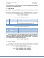
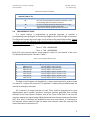
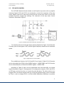
California State University, Northridge ECE Department ECE425L, Fall 2011 By: Xiaojun Geng Lab Experiment 11: General Purpose Timers 1 Introduction General purpose timers/counters are common subsystems of microcontroller systems, which typically include a free running counter and multiple inputcapture/output-match pins. The LPC2148 has two functionally identical general purpose timers: Timer 0 and Timer 1. In this lab, output matches will be configured to generate periodical interrupts to the processor for the purposing of driving step motors. The objectives of this experiment include: to learn functionalities of General Purpose Timer systems to gain thorough familiarity with the Vectored Interrupt Controllers to practice on configuring interrupts and writing interrupt service routines 2 Lab Preparation Please prepare the lab (e.g., read this section, write the needed Assembly code, assemble them to eliminate any syntax error) before you come to the laboratory. If possible, you may run your code with RealView Microcontroller Development Kit (RMDK) simulator. This will help you to complete the required task on time. 2.1 THE FREE RUNNING COUNTER The heart of the Timers of the LPC2148 microcontroller is a 32-bit free-running counter, which is designed to count cycles of the peripheral clock (PCLK) or an externally supplied clock. This counter is programmable with a 32-bit prescaler, as illustrated in Figure 1. Figure 1. A 32-bit timer counter with a 32-bit prescaler The tick rate of the Timer Counter (TC) is controlled by the 32-bit number written in the Prescaler Register (PR) in the following way. There is a Prescaler Counter (PC) which increments on each tick of the PCLK. When it reaches the value in the Prescaler Register, the Timer count is incremented and the Prescaler Counter is reset, on the next PCLK. This causes the Timer Counter to increment on every PCLK when PR = 0, every 2 PCLKs when PR = 1, etc. The addresses allocated to the Prescaler Registers for the Timer 0 / 1 are: Timer 0: T0PR – 0xE000 400C Timer 1: T1PR – 0xE000 800C The peripheral clock PCLK is derived from the processor clock CLCK. The processor clock operates at 12MHz frequency for the LPC2148 on the Education board when the 1 California State University, Northridge ECE Department ECE425L, Fall 2011 By: Xiaojun Geng Phase-Locked Loop (PLL) is not programmed. The default condition at reset lets the PCLK run at one quarter of the processor speed. 2.2 TIMER CONTROL The Timer Control Register (TCR) is used to control the operation of the Timer. The Timer could be enabled or disabled with the bit 0 of the register; and the Timer could be reset and stays being reset with the bit 1 of TCR. The detailed description of the register bits is listed in Table 1. The addresses allocated to TCRs of the Timer 0 and Timer 1 are: Timer 0: T0TCR – 0xE000 4004 Timer 1: T1TCR – 0xE000 8004 Table 1. Timer Control Register (TCR) Bit Description Bit 0 Symbol Counter Enable 1 Counter Reset 7:2 - Description When one, the Timer Counter and Prescale Counter are enabled for counting. When zero, the counters are disabled. When one, the Timer Counter and the Prescale Counter are synchronously reset on the next positive edge of PCLK. The counters remain reset until this bit is returned to zero. Reserved. User software should not write ones to reserved bits. Table 2. Count Control Register (CTCR) Bit Description Bit 1:0 Symbol Counter/Timer Mode 3:2 7-4 Count Input Select - Value 00 01,10,11 00,01,10,11 - Description Timer Mode: every rising PCLK edge. Counter Mode. See LPC2148 user manual for details. See LPC2148 user manual for details on capture function. Reserved. User software should not write ones to reserved bits. The Timer Counter could be set in Timer Mode, counting PCLK(PR+1) as illustrated in Figure 1, or in Counter Mode, counting the external edges on selected input capture pin. Such function selection is configured with the Count Control register (CTCR) shown in Table 2 , mapped with the following memory addresses: Timer 0: T0CTCR – 0xE000 4070 Timer 1: T1CTCR – 0xE000 8070 2.3 OUTPUT MATCHES In addition to the basic timer counter, each timer has four match (or compare) channels. Each match channel has a match register (MR0-MR3) which can be written with a 32-bit number, with the following memory addresses: Timer 0: T0MR0– 0xE0004018, T0MR1– 0xE000401C, T0MR2 – 0xE0004020, T0MR0 – 0xE0004024 Timer 1: T1MR0– 0xE0008018, T1MR1– 0xE000801C, T1MR2 – 0xE0008020, T1MR0 – 0xE0008024 2 California State University, Northridge ECE Department ECE425L, Fall 2011 By: Xiaojun Geng The current value of the Timer Counter is compared with the Match Register value. When the two values are equal, actions can be triggered automatically. The possible actions include generating an interrupt, resetting the Timer Counter, or stopping the Timer Counter. Actions are selected by the bits in the Match Control Register (MCR) with the following memory allocations: Timer 0: T0MCR – 0xE000 4014 Timer 1: T1MCR – 0xE000 8014 The function of each of the bits of MCR is shown in Table 3 and Table 4. Table 3. Match Control Register (MCR) Bit Symbol Bit Symbol 15-12 Reserved 6 MR2I 5 MR1S 11 MR3S 4 MR1R 10 MR3R 3 MR1I 9 MR3I 2 MR0S 8 MR2S 1 MR0R 7 MR2R 0 MR0I Table 4. Symbol Description in Match Control Register Symbol MRnI MRnR MRnS Value 1 0 1 0 1 0 Description (“n” = 0, 1, 2, 3) An interrupt is generated when MRx matches the value in TC. This interrupt is disabled. The TC will be reset when MRx matches it. This feature is disabled. The TC and PC will be stopped and disabled if MRx matches the TC. This feature is disabled. Besides the events listed in Table 4, when a match occurs, each output match channel has an associated match pin (labeled as MAT) which can be modified. The match outputs are reflected by the lower 4 status bits of the External Match Register (EMR): Timer 0: T0EMR – 0xE000 403C Timer 1: T1EMR – 0xE000 803C The description of these four bits is described in Table 5. The bits [11:4] of the EMR are control bits which select the actions to be carried out when a match event occurs, for which the details are described in Table 6. Table 5. External Match Register (EMR) Bit Description Bit 0 Symbol EM0 1 EM1 2 EM2 3 EM3 Description External Match 0. This bit reflects the state of output MAT0.0/MAT1.0. When a match occurs between the TC and MR0, this output of the timer can either toggle, go low, go high, or do nothing. Bits EMR[5:4] control the functionality of this output. External Match 1. This bit reflects the state of output MAT0.1/MAT1.1. Bits EMR[7:6] control the functionality of this output. External Match 2. This bit reflects the state of output MAT0.2/MAT1.2. Bits EMR[9:8] control the functionality of this output. External Match 3. This bit reflects the state of output MAT0.3/MAT1.3. Bits EMR[11:10] control the functionality of this output. 3 California State University, Northridge ECE Department ECE425L, Fall 2011 By: Xiaojun Geng Table 6. External Match Control Bits. EMR [5:4], EMR [7:6] EMR [9:8], EMR [11:10] 00 01 10 11 Function Do nothing. Clear the corresponding External Match bit/output to 0 (the corresponding MAT pin is LOW if pinned out). Set the corresponding External Match bit/output to 0 (the corresponding MAT pin is High if pinned out). Toggle the corresponding External Match bit/output. 2.4 TIME INTERRUPT FLAGS If a match channel is programmed to generate interrupts at matches, a corresponding interrupt flag bit in the Interrupt Register (IR) will be set high at the match. The flag bit will remain high until a logic one is written to the same IR bit location. Always remember to reset the interrupt in the interrupt service routine by writing a logic one to the corresponding IR bit. Writing a zero to the IR bit has no effect. The memory address mapped to IR for each timer is: Timer 0: T0IR – 0xE000 4000 Timer 1: T1IR – 0xE000 8000 Bit 0 of IR is the interrupt flag for match channel 0, and bit 1 is for channel 1, and so on. The detailed bit description is shown in Table 7. Table 7. Interrupt Register Bit Description Bit 0 1 2 3 4 5 6 7 Symbol MR0 Interrupt MR0 Interrupt MR0 Interrupt MR0 Interrupt CR0 Interrupt CR1 Interrupt CR2 Interrupt CR3 Interrupt Description Interrupt flag for match channel 0. Interrupt flag for match channel 1. Interrupt flag for match channel 2. Interrupt flag for match channel 3. Interrupt flag for capture channel 0 event. Interrupt flag for capture channel 1 event. Interrupt flag for capture channel 2 event. Interrupt flag for capture channel 3 event. The flags in the IR register can be polled (i.e., being read constantly) in order to know if a match or a capture has occurred. This approach is called polling to differentiate the method of waiting for interrupts. All 4 channels of output matches of each Timer could be programmed to work independently and in parallel, therefore, interrupts could be generated from multiple channels of the Timer system. However, each of the Timer 0 and Timer 1 has only one interrupt request line (signals being ORed) connected to the Vectored Interrupt Controller (VIC). As a result, if interrupts are enabled for more than one channel, it is necessary in the interrupt service routine to find out which timer channel causes the interrupt. See more information in the Section 2.7. 4 California State University, Northridge ECE Department 2.5 ECE425L, Fall 2011 By: Xiaojun Geng STEP MOTOR CONTROL The LPC2148 Education Board includes a small bipolar step motor with a propeller mounted. Signals P0.12 and P0.21 are connected to control the movement of the step motor. Bipolar control of a step motor means that the current must flow in one (of two possible) directions through the windings. The schematic of the step motor control interface is illustrated in Figure 2. Figure 2. LPC2148 Education Board Schematic: Step Motor Control. To rotate the axis one of the two output patterns depicted in Figure 3 must be used. The duty cycle of both signals is 50%, and the signal frequency determines the rotational speed. Figure 3. Signal Patterns for the Step Motor. The available pin functions for P0.12 and P0.21 are listed in Table 8. P0.12 function can be selected by bits [25:24] of the PINSEL0 register – 0xE002 C000, and P0.21 function can be selected by bits [11:10] of the PINSEL1 register – 0xE002 C004. According to Table 8, there are two approaches that microcontroller can output signals illustrated in Figure 3. One approach is to configure the two pins, P0.12 and P0.21, as GPIO pins, and use the timer to control the pulse durations. The other solution is to program P0.12 as external output match pin so that the pulse durations can be controlled by Timer 1, and to configure P0.21 as a Pulse Width Modulation (PWM) pin to produce 5 California State University, Northridge ECE Department ECE425L, Fall 2011 By: Xiaojun Geng the square wave. In either situation, you need to calculate the number of Timer ticks for a proper pulse width. Table 8. Pin Function Selection for P0.12 and P0.21 Register Bits PINSEL0[25:24] Pin P0.12 PINSEL1[11:10] P0.21 Value 00 01 10 11 00 01 10 11 Function GPIO Port 0.12 DSR (UART1) Match 1.0 (Timer 1) AD1.3 GPIO Port 0.21 PWM5 AD1.6 Capture 1.3 (Timer 1) 2.6 VECTORED INTERRUPT CONTROLLER As stated in earlier section, the four channels of each Timer (Timer 0 and 1) may be configured independently to generate interrupt requests, and these requests are ORed before connecting to the Vectored Interrupt Controller (VIC). In fact, similar to the Timers, each peripheral device on the LPC2148 has only one interrupt line connected to the VIC, but may have several internal interrupt flags. The Interrupt Select register (VICIntSelect – 0xFFFF F00C) classifies each interrupt source as contributing to FIQ or IRQ. Each interrupt source is allocated with one bit location in this register. Such bit location is called the channel number for that interrupt source. For example, the Timer 0 is assigned with channel 4 and the Timer 1 with channel 5, as shown in Table 9. Table 9. VICIntSelect Register Bits for Timers Bit VICIntSelect [4] Symbol TIMER0 VICIntSelect [5] TIMER1 Value 0 1 0 1 Description The Timer 0 interrupt is assigned to the IRQ category The Timer 0 interrupt is assigned to the FIQ category The Timer 1 interrupt is assigned to the IRQ category The Timer 1 interrupt is assigned to the FIQ category Each of these interrupt sources can be enabled or disabled by configuring the Interrupt Enable register (VICIntEnable – 0xFFFF F010). As in the VICIntSelect, the same bit location (or channel number) is assigned to each interrupt source in the VICIntEnable register. Writing a “1” in a bit location enables the corresponding interrupt source to contribute to FIQ or IRQ; and writing a “0” has no effect. The reset value of the register is 0. See Table 10 for details. To disable a certain interrupt source, we need to write a “1” to the bit location (i.e., the channel number) assigned to the peripheral in the Interrupt Enable Clear register 6 California State University, Northridge ECE Department ECE425L, Fall 2011 By: Xiaojun Geng (VICIntEnClear – 0xFFFF F014). This register allows software to clear one or more bits in the VICIntEnable register without first reading it. Table 10. VICIntEnable Register Bits for Timers Bit VICIntEnable [4] Symbol TIMER0 VICIntEnable [5] TIMER1 Access Read Write Read Write Description “1” indicates that the Timer 0 interrupt is enabled. Writing a “1” to this bit enables the Timer 0 interrupt. “1” indicates that the Timer 1 interrupt is enabled. Writing a “1” to this bit enables the Timer 1 interrupt. 2.7 VECTORED IRQS Normally in an application with multiple interrupt sources, only one interrupt source is defined as FIQ, and the rest are defined as IRQs. In the IRQ category, interrupts can be further classified as non-vectored IRQs and vectored IRQs. The non-vectored IRQs share the same interrupt vector address, while vectored IRQs could each have its own vector address. For these vectored IRQs, the Vectored Interrupt Controller (VIC) builds a programmable hardware lookup table and delivers the address of service routine of a certain interrupt source to the processor when interrupts occur. More specially, the VIC contains 16 slots for vectored IRQs. Slot 0 has the highest priority and slot 15 the lowest. Each slot is associated with a vector control register and a vector address register, which are: VICVectCntl0 – 0xFFFF F200, VICVectCntl1 – 0xFFFF F204, …, VICVectCntl15 – 0xFFFF F23C VICVectAddr0 – 0xFFFFF100, VICVectAddr1 – 0xFFFFF104, …, VICVectAddr15– 0xFFFFF13C Interrupt sources can be assigned to any of the 16 slots by configuring the above two registers. Details of the configuration will be explained below. Firstly, the vector control register for each slot has two fields: a channel field and an enable bit. Bit [4:0] is the channel number of the interrupt source assigned to this vectored IRQ slot. For example, to assign the Timer 1 in the slot 8, we program VICVectCntl8[4:0] with 5. Bit 5 of the vector control register is the enabling bit; and when being “1”, a unique interrupt handler address is used for this interrupt source. The rest of the bits in the vector control register are reserved, and writing ones are not allowed to reserved bits. Secondly, each VIC slot has a vector address register, VICVectAddr. It will be used to hold the interrupt handler address for the interrupt source assigned to this slot. Stated below is how the VIC handles the vectored IRQs in practice. Suppose that an interrupt source is configured and enabled in the VIC slot 3. When an interrupt request is generated from this source, the address stored in the VICVectAddr3 register will be loaded into a fixed memory location called the Vector Address Register (VICVectAddr – 0xFFFF F030). On the other hand, the processor still jumps to the normal entry of IRQ mode, and read the contents of the IRQ vector address 0x00000018. In order for the processor to find the right service routine address, the following instruction needs to be placed at 0x00000018 (think why): 7 California State University, Northridge ECE Department LDR ECE425L, Fall 2011 By: Xiaojun Geng pc, [pc,#-0xFF0] Now you know how to configure the VIC for the vectored IRQs. There is one more thing you need to remember when writing interrupt service routines (ISR) for vectored IRQs. That is, at the end of ISR for a vectored IRQ, you must make a dummy write to the Vector Address Register (VICVectAddr) to signal the processor that the service routine is about to complete. 3 Lab Tasks For the tasks below, complete the following requirements: Create ARM assembly program for all the tasks BEFORE coming to the lab. Simulate your code and verify the result with the debugger to make sure that the program sends the correct data to the control registers and port pins. Download the machine code in HEX file to the LPC2148 microcontroller, and verity the result after execution. Demonstrate the results to the lab instructor before you leave the lab. Task 1: Write a complete program to generate proper square pulses on GPIO pins, P0.12 and P0.21, to rotate the propeller, with the method of polling timer interrupt flags. Task 2: Write a complete program to generate proper square pulses on GPIO pins, P0.12 and P0.21, to rotate the propeller, by configuring the timer interrupt as a non-vectored IRQ. Task 3: Write a complete program to generate proper square pulses on GPIO pins, P0.12 and P0.21, to rotate the propeller, by configuring the timer interrupt as a vectored IRQ. 4 Requirements: A. This is a two-week lab experiment. Pre-lab work will be checked in the beginning of the lab time. It is very important to complete your pre-lab which includes reading through Section 2 of this handout, and write assembly code for all the tasks. B. Lab report is DUE one week after the lab time. The report should include your names, experiment objectives, experiment problems, the print-out of your work, explanation and discussion, and conclusion. C. Demonstrate your results to the instructor before you leave. Failure to do so will result in zero point for performance. 8