1
RM0038
Reference manual
STM32L100xx, STM32L151xx, STM32L152xx and STM32L162xx
advanced ARM®-based 32-bit MCUs
Introduction
This reference manual targets application developers. It provides complete information on
how to use the STM32L151xx, STM32L152xx and STM32L162xx and STM32L100xx
microcontroller memory and peripherals. The STM32L151xx, STM32L152xx and
STM32L162xx and STM32L100xx value line will be referred to as STM32L1xxxx throughout
the document, unless otherwise specified.
The STM32L1xxxx is a family of microcontrollers with different memory sizes, packages and
peripherals.
For ordering information, mechanical and electrical device characteristics please refer to the
corresponding datasheets.
For information on programming, erasing and protection of the internal non volatile memory
please refer to Section 3: Flash program memory and data EEPROM (FLASH).
For information on the ARM® Cortex®-M3 core, please refer to the Cortex®-M3 Technical
Reference Manual.
Related documents
Available from www.arm.com:
• Cortex®-M3 Technical Reference Manual, available from http://infocenter.arm.com
Available from www.st.com:
• STM32L151xx STM32L152xx datasheets
• STM32L162xx datasheet
• STM32L100xx datasheet
• STM32F10xxx/20xxx/21xxx/L1xxxx Cortex®-M3 programming manual
• Migrating from STM32L15xx6/8/B to STM32L15xx6/8/B-A and from STM32L100x6/8/B to
STM32L100x6/8/B-A (TN1176)
• Migrating from STM32L15/6xRC-A to STM32L15/6xRC and from STM32L15/6xVC-A to
STM32L15/6xVC (TN1177)
• Migrating from STM32L15/6xxD to STM32L15/6xxE (TN1178)
• Migrating from STM32L15/6xxD to STM32L15/6xVD-X (TN1201)
July 2015
DocID15965 Rev 13
1/901
www.st.com
1
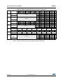
Contents
RM0038
Contents
1
2
3
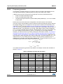
Documentation conventions . . . . . . . . . . . . . . . . . . . . . . . . . . . . . . . . . 38
1.1
List of abbreviations for registers . . . . . . . . . . . . . . . . . . . . . . . . . . . . . . . 38
1.2
Peripheral availability . . . . . . . . . . . . . . . . . . . . . . . . . . . . . . . . . . . . . . . . 38
1.3
Glossary . . . . . . . . . . . . . . . . . . . . . . . . . . . . . . . . . . . . . . . . . . . . . . . . . . 39
1.4
Product category definition . . . . . . . . . . . . . . . . . . . . . . . . . . . . . . . . . . . . 40
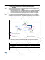
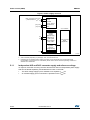
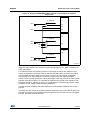
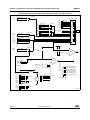
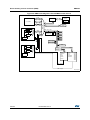
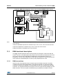
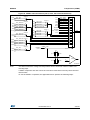
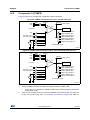
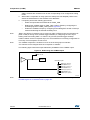
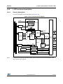
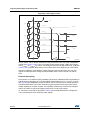
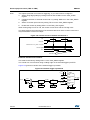
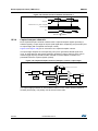
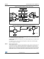
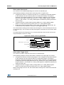
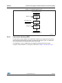
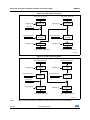
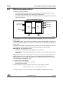
System architecture and memory overview . . . . . . . . . . . . . . . . . . . . . 42
2.1
System architecture . . . . . . . . . . . . . . . . . . . . . . . . . . . . . . . . . . . . . . . . . 42
2.2
Memory organization . . . . . . . . . . . . . . . . . . . . . . . . . . . . . . . . . . . . . . . . 46
2.3
Memory map . . . . . . . . . . . . . . . . . . . . . . . . . . . . . . . . . . . . . . . . . . . . . . 46
2.4
Embedded SRAM . . . . . . . . . . . . . . . . . . . . . . . . . . . . . . . . . . . . . . . . . . . 49
2.5
NVM overview . . . . . . . . . . . . . . . . . . . . . . . . . . . . . . . . . . . . . . . . . . . . . 49
2.6
Bit banding . . . . . . . . . . . . . . . . . . . . . . . . . . . . . . . . . . . . . . . . . . . . . . . . 49
2.7
Boot configuration . . . . . . . . . . . . . . . . . . . . . . . . . . . . . . . . . . . . . . . . . . 50
Flash program memory and data EEPROM (FLASH) . . . . . . . . . . . . . . 52
3.1
NVM introduction . . . . . . . . . . . . . . . . . . . . . . . . . . . . . . . . . . . . . . . . . . . 52
3.2
NVM organization . . . . . . . . . . . . . . . . . . . . . . . . . . . . . . . . . . . . . . . . . . . 52
3.3
Read interface . . . . . . . . . . . . . . . . . . . . . . . . . . . . . . . . . . . . . . . . . . . . . 59
3.4
3.5
3.3.1
Relation between CPU clock frequency and Flash memory read time . 59
3.3.2
Instruction prefetch when Flash access is 64 bits . . . . . . . . . . . . . . . . . 60
3.3.3
Data management . . . . . . . . . . . . . . . . . . . . . . . . . . . . . . . . . . . . . . . . . 61
Memory operations . . . . . . . . . . . . . . . . . . . . . . . . . . . . . . . . . . . . . . . . . . 62
3.4.1
Unlocking/locking memory . . . . . . . . . . . . . . . . . . . . . . . . . . . . . . . . . . . 62
3.4.2
Erasing memory . . . . . . . . . . . . . . . . . . . . . . . . . . . . . . . . . . . . . . . . . . . 63
3.4.3
Programming memory . . . . . . . . . . . . . . . . . . . . . . . . . . . . . . . . . . . . . . 65
3.4.4
Read while write (RWW) . . . . . . . . . . . . . . . . . . . . . . . . . . . . . . . . . . . . 70
Option byte description . . . . . . . . . . . . . . . . . . . . . . . . . . . . . . . . . . . . . . . 73
3.5.1
3.6
Quick reference to programming/erase functions . . . . . . . . . . . . . . . . . . 77
3.7
Memory protection . . . . . . . . . . . . . . . . . . . . . . . . . . . . . . . . . . . . . . . . . . 80
3.7.1
2/901
Option byte block programming . . . . . . . . . . . . . . . . . . . . . . . . . . . . . . . 77
Readout protection (RDP) of the program and data EEPROMs . . . . . . 80
DocID15965 Rev 13
RM0038
4
5
Contents
3.7.2
Write protection (WRP) of the program memory . . . . . . . . . . . . . . . . . . 82
3.7.3
Write protection error flag . . . . . . . . . . . . . . . . . . . . . . . . . . . . . . . . . . . 82
3.7.4
PCROP . . . . . . . . . . . . . . . . . . . . . . . . . . . . . . . . . . . . . . . . . . . . . . . . . 82
3.8
Interrupts . . . . . . . . . . . . . . . . . . . . . . . . . . . . . . . . . . . . . . . . . . . . . . . . . 83
3.9
Register description . . . . . . . . . . . . . . . . . . . . . . . . . . . . . . . . . . . . . . . . . 83
3.9.1
Access control register (FLASH_ACR) . . . . . . . . . . . . . . . . . . . . . . . . . 83
3.9.2
Program/erase control register (FLASH_PECR) . . . . . . . . . . . . . . . . . . 84
3.9.3
Power down key register (FLASH_PDKEYR) . . . . . . . . . . . . . . . . . . . . 87
3.9.4
Program/erase key register (FLASH_PEKEYR) . . . . . . . . . . . . . . . . . . 87
3.9.5
Program memory key register (FLASH_PRGKEYR) . . . . . . . . . . . . . . . 87
3.9.6
Option byte key register (FLASH_OPTKEYR) . . . . . . . . . . . . . . . . . . . . 88
3.9.7
Status register (FLASH_SR) . . . . . . . . . . . . . . . . . . . . . . . . . . . . . . . . . 88
3.9.8
Option byte register (FLASH_OBR) . . . . . . . . . . . . . . . . . . . . . . . . . . . . 90
3.9.9
Write protection register (FLASH_WRPRx) . . . . . . . . . . . . . . . . . . . . . . 91
3.9.10
Register map . . . . . . . . . . . . . . . . . . . . . . . . . . . . . . . . . . . . . . . . . . . . . 91
CRC calculation unit . . . . . . . . . . . . . . . . . . . . . . . . . . . . . . . . . . . . . . . . 94
4.1
CRC introduction . . . . . . . . . . . . . . . . . . . . . . . . . . . . . . . . . . . . . . . . . . . 94
4.2
CRC main features . . . . . . . . . . . . . . . . . . . . . . . . . . . . . . . . . . . . . . . . . . 94
4.3
CRC functional description . . . . . . . . . . . . . . . . . . . . . . . . . . . . . . . . . . . . 95
4.4
CRC registers . . . . . . . . . . . . . . . . . . . . . . . . . . . . . . . . . . . . . . . . . . . . . . 95
4.4.1
Data register (CRC_DR) . . . . . . . . . . . . . . . . . . . . . . . . . . . . . . . . . . . . 95
4.4.2
Independent data register (CRC_IDR) . . . . . . . . . . . . . . . . . . . . . . . . . 95
4.4.3
Control register (CRC_CR) . . . . . . . . . . . . . . . . . . . . . . . . . . . . . . . . . . 96
4.4.4
CRC register map . . . . . . . . . . . . . . . . . . . . . . . . . . . . . . . . . . . . . . . . . 96
Power control (PWR) . . . . . . . . . . . . . . . . . . . . . . . . . . . . . . . . . . . . . . . . 97
5.1
Power supplies . . . . . . . . . . . . . . . . . . . . . . . . . . . . . . . . . . . . . . . . . . . . . 97
5.1.1
Independent A/D and DAC converter supply and reference voltage . . . 98
5.1.2
Independent LCD supply . . . . . . . . . . . . . . . . . . . . . . . . . . . . . . . . . . . . 99
5.1.3
RTC and RTC backup registers . . . . . . . . . . . . . . . . . . . . . . . . . . . . . . . 99
5.1.4
Voltage regulator . . . . . . . . . . . . . . . . . . . . . . . . . . . . . . . . . . . . . . . . . 100
5.1.5
Dynamic voltage scaling management . . . . . . . . . . . . . . . . . . . . . . . . 100
5.1.6
Dynamic voltage scaling configuration . . . . . . . . . . . . . . . . . . . . . . . . 102
5.1.7
Voltage regulator and clock management when VDD drops
below 2.0 V . . . . . . . . . . . . . . . . . . . . . . . . . . . . . . . . . . . . . . . . . . . . . 103
DocID15965 Rev 13
3/901
26
Contents
RM0038
5.1.8
5.2
5.3
5.4
6
Power supply supervisor . . . . . . . . . . . . . . . . . . . . . . . . . . . . . . . . . . . . 103
5.2.1
Power on reset (POR)/power down reset (PDR) . . . . . . . . . . . . . . . . . 105
5.2.2
Brown out reset . . . . . . . . . . . . . . . . . . . . . . . . . . . . . . . . . . . . . . . . . . 106
5.2.3
Programmable voltage detector (PVD) . . . . . . . . . . . . . . . . . . . . . . . . 107
5.2.4
Internal voltage reference (VREFINT) . . . . . . . . . . . . . . . . . . . . . . . . . 108
Low-power modes . . . . . . . . . . . . . . . . . . . . . . . . . . . . . . . . . . . . . . . . . 108
5.3.1
Behavior of clocks in low power modes . . . . . . . . . . . . . . . . . . . . . . . . 109
5.3.2
Slowing down system clocks . . . . . . . . . . . . . . . . . . . . . . . . . . . . . . . . 110
5.3.3
Peripheral clock gating . . . . . . . . . . . . . . . . . . . . . . . . . . . . . . . . . . . . 110
5.3.4
Low power run mode (LP run) . . . . . . . . . . . . . . . . . . . . . . . . . . . . . . . 111
5.3.5
Sleep mode . . . . . . . . . . . . . . . . . . . . . . . . . . . . . . . . . . . . . . . . . . . . . 111
5.3.6
Low power sleep mode (LP sleep) . . . . . . . . . . . . . . . . . . . . . . . . . . . 113
5.3.7
Stop mode . . . . . . . . . . . . . . . . . . . . . . . . . . . . . . . . . . . . . . . . . . . . . . 114
5.3.8
Standby mode . . . . . . . . . . . . . . . . . . . . . . . . . . . . . . . . . . . . . . . . . . . 116
5.3.9
Waking up the device from Stop and Standby modes using the RTC
and comparators . . . . . . . . . . . . . . . . . . . . . . . . . . . . . . . . . . . . . . . . . 117
Power control registers . . . . . . . . . . . . . . . . . . . . . . . . . . . . . . . . . . . . . . 120
5.4.1
PWR power control register (PWR_CR) . . . . . . . . . . . . . . . . . . . . . . . 120
5.4.2
PWR power control/status register (PWR_CSR) . . . . . . . . . . . . . . . . . 123
5.4.3
PWR register map . . . . . . . . . . . . . . . . . . . . . . . . . . . . . . . . . . . . . . . . 124
Reset and clock control (RCC) . . . . . . . . . . . . . . . . . . . . . . . . . . . . . . . 126
6.1
6.2
4/901
Voltage regulator and clock management when modifying the
VCORE range . . . . . . . . . . . . . . . . . . . . . . . . . . . . . . . . . . . . . . . . . . . 103
Reset . . . . . . . . . . . . . . . . . . . . . . . . . . . . . . . . . . . . . . . . . . . . . . . . . . . 126
6.1.1
System reset . . . . . . . . . . . . . . . . . . . . . . . . . . . . . . . . . . . . . . . . . . . . 126
6.1.2
Power reset . . . . . . . . . . . . . . . . . . . . . . . . . . . . . . . . . . . . . . . . . . . . . 127
6.1.3
RTC and backup registers reset . . . . . . . . . . . . . . . . . . . . . . . . . . . . . 127
Clocks . . . . . . . . . . . . . . . . . . . . . . . . . . . . . . . . . . . . . . . . . . . . . . . . . . . 128
6.2.1
HSE clock . . . . . . . . . . . . . . . . . . . . . . . . . . . . . . . . . . . . . . . . . . . . . . 130
6.2.2
HSI clock . . . . . . . . . . . . . . . . . . . . . . . . . . . . . . . . . . . . . . . . . . . . . . . 131
6.2.3
MSI clock . . . . . . . . . . . . . . . . . . . . . . . . . . . . . . . . . . . . . . . . . . . . . . . 131
6.2.4
PLL . . . . . . . . . . . . . . . . . . . . . . . . . . . . . . . . . . . . . . . . . . . . . . . . . . . 132
6.2.5
LSE clock . . . . . . . . . . . . . . . . . . . . . . . . . . . . . . . . . . . . . . . . . . . . . . . 133
6.2.6
LSI clock . . . . . . . . . . . . . . . . . . . . . . . . . . . . . . . . . . . . . . . . . . . . . . . 133
6.2.7
System clock (SYSCLK) selection . . . . . . . . . . . . . . . . . . . . . . . . . . . . 134
6.2.8
System clock source frequency versus voltage range . . . . . . . . . . . . . 134
DocID15965 Rev 13
RM0038
Contents
6.3
7
6.2.9
Clock security system (CSS) . . . . . . . . . . . . . . . . . . . . . . . . . . . . . . . . 134
6.2.10
Clock Security System on LSE . . . . . . . . . . . . . . . . . . . . . . . . . . . . . . 135
6.2.11
RTC and LCD clock . . . . . . . . . . . . . . . . . . . . . . . . . . . . . . . . . . . . . . . 135
6.2.12
Watchdog clock . . . . . . . . . . . . . . . . . . . . . . . . . . . . . . . . . . . . . . . . . . 135
6.2.13
Clock-out capability . . . . . . . . . . . . . . . . . . . . . . . . . . . . . . . . . . . . . . . 136
6.2.14
Internal/external clock measurement with TIM9/TIM10/TIM11 . . . . . . 136
6.2.15
Clock-independent system clock sources for TIM9/TIM10/TIM11 . . . . 138
RCC registers . . . . . . . . . . . . . . . . . . . . . . . . . . . . . . . . . . . . . . . . . . . . . 139
6.3.1
Clock control register (RCC_CR) . . . . . . . . . . . . . . . . . . . . . . . . . . . . . 139
6.3.2
Internal clock sources calibration register (RCC_ICSCR) . . . . . . . . . . 141
6.3.3
Clock configuration register (RCC_CFGR) . . . . . . . . . . . . . . . . . . . . . 141
6.3.4
Clock interrupt register (RCC_CIR) . . . . . . . . . . . . . . . . . . . . . . . . . . . 144
6.3.5
AHB peripheral reset register (RCC_AHBRSTR) . . . . . . . . . . . . . . . . 147
6.3.6
APB2 peripheral reset register (RCC_APB2RSTR) . . . . . . . . . . . . . . 149
6.3.7
APB1 peripheral reset register (RCC_APB1RSTR) . . . . . . . . . . . . . . 150
6.3.8
AHB peripheral clock enable register (RCC_AHBENR) . . . . . . . . . . . 153
6.3.9
APB2 peripheral clock enable register (RCC_APB2ENR) . . . . . . . . . . 155
6.3.10
APB1 peripheral clock enable register (RCC_APB1ENR) . . . . . . . . . . 157
6.3.11
AHB peripheral clock enable in low power mode register
(RCC_AHBLPENR) . . . . . . . . . . . . . . . . . . . . . . . . . . . . . . . . . . . . . . . 159
6.3.12
APB2 peripheral clock enable in low power mode register
(RCC_APB2LPENR) . . . . . . . . . . . . . . . . . . . . . . . . . . . . . . . . . . . . . . 161
6.3.13
APB1 peripheral clock enable in low power mode register
(RCC_APB1LPENR) . . . . . . . . . . . . . . . . . . . . . . . . . . . . . . . . . . . . . . 163
6.3.14
Control/status register (RCC_CSR) . . . . . . . . . . . . . . . . . . . . . . . . . . . 165
6.3.15
RCC register map . . . . . . . . . . . . . . . . . . . . . . . . . . . . . . . . . . . . . . . . 168
General-purpose I/Os (GPIO) . . . . . . . . . . . . . . . . . . . . . . . . . . . . . . . . 171
7.1
GPIO introduction . . . . . . . . . . . . . . . . . . . . . . . . . . . . . . . . . . . . . . . . . . 171
7.2
GPIO main features . . . . . . . . . . . . . . . . . . . . . . . . . . . . . . . . . . . . . . . . 171
7.3
GPIO functional description . . . . . . . . . . . . . . . . . . . . . . . . . . . . . . . . . . 171
7.3.1
General-purpose I/O (GPIO) . . . . . . . . . . . . . . . . . . . . . . . . . . . . . . . . 174
7.3.2
I/O pin multiplexer and mapping . . . . . . . . . . . . . . . . . . . . . . . . . . . . . 174
7.3.3
I/O port control registers . . . . . . . . . . . . . . . . . . . . . . . . . . . . . . . . . . . 176
7.3.4
I/O port data registers . . . . . . . . . . . . . . . . . . . . . . . . . . . . . . . . . . . . . 177
7.3.5
I/O data bitwise handling . . . . . . . . . . . . . . . . . . . . . . . . . . . . . . . . . . . 177
7.3.6
GPIO locking mechanism . . . . . . . . . . . . . . . . . . . . . . . . . . . . . . . . . . 177
7.3.7
I/O alternate function input/output . . . . . . . . . . . . . . . . . . . . . . . . . . . . 178
DocID15965 Rev 13
5/901
26
Contents
RM0038
7.4
8
7.3.8
External interrupt/wakeup lines . . . . . . . . . . . . . . . . . . . . . . . . . . . . . . 178
7.3.9
Input configuration . . . . . . . . . . . . . . . . . . . . . . . . . . . . . . . . . . . . . . . . 178
7.3.10
Output configuration . . . . . . . . . . . . . . . . . . . . . . . . . . . . . . . . . . . . . . 179
7.3.11
Alternate function configuration . . . . . . . . . . . . . . . . . . . . . . . . . . . . . . 179
7.3.12
Analog configuration . . . . . . . . . . . . . . . . . . . . . . . . . . . . . . . . . . . . . . 180
7.3.13
Using the OSC32_IN/OSC32_OUT pins as GPIO PC14/PC15
port pins . . . . . . . . . . . . . . . . . . . . . . . . . . . . . . . . . . . . . . . . . . . . . . . . 181
7.3.14
Using the OSC_IN/OSC_OUT pins as GPIO PH0/PH1 port pins . . . . 181
7.3.15
Selection of RTC_AF1 alternate functions . . . . . . . . . . . . . . . . . . . . . . 181
GPIO registers . . . . . . . . . . . . . . . . . . . . . . . . . . . . . . . . . . . . . . . . . . . . 183
7.4.1
GPIO port mode register (GPIOx_MODER) (x = A..H) . . . . . . . . . . . . 183
7.4.2
GPIO port output type register (GPIOx_OTYPER)
(x = A..H) . . . . . . . . . . . . . . . . . . . . . . . . . . . . . . . . . . . . . . . . . . . . . . . 183
7.4.3
GPIO port output speed register (GPIOx_OSPEEDR)
(x = A..H) . . . . . . . . . . . . . . . . . . . . . . . . . . . . . . . . . . . . . . . . . . . . . . . 184
7.4.4
GPIO port pull-up/pull-down register (GPIOx_PUPDR)
(x = A..H) . . . . . . . . . . . . . . . . . . . . . . . . . . . . . . . . . . . . . . . . . . . . . . . 184
7.4.5
GPIO port input data register (GPIOx_IDR) (x = A..H) . . . . . . . . . . . . 185
7.4.6
GPIO port output data register (GPIOx_ODR) (x = A..H) . . . . . . . . . . 185
7.4.7
GPIO port bit set/reset register (GPIOx_BSRR) (x = A..H) . . . . . . . . . 185
7.4.8
GPIO port configuration lock register (GPIOx_LCKR)
(x = A..H) . . . . . . . . . . . . . . . . . . . . . . . . . . . . . . . . . . . . . . . . . . . . . . . 186
7.4.9
GPIO alternate function low register (GPIOx_AFRL) (x = A..H) . . . . . 187
7.4.10
GPIO alternate function high register (GPIOx_AFRH)
(x = A..H) . . . . . . . . . . . . . . . . . . . . . . . . . . . . . . . . . . . . . . . . . . . . . . . 188
7.4.11
GPIO bit reset register (GPIOx_BRR) (x = A..H) . . . . . . . . . . . . . . . . . 188
7.4.12
GPIO register map . . . . . . . . . . . . . . . . . . . . . . . . . . . . . . . . . . . . . . . . 188
System configuration controller (SYSCFG) and
routing interface (RI) . . . . . . . . . . . . . . . . . . . . . . . . . . . . . . . . . . . . . . . 191
8.1
SYSCFG and RI introduction . . . . . . . . . . . . . . . . . . . . . . . . . . . . . . . . . 191
8.2
RI main features . . . . . . . . . . . . . . . . . . . . . . . . . . . . . . . . . . . . . . . . . . . 191
8.3
RI functional description . . . . . . . . . . . . . . . . . . . . . . . . . . . . . . . . . . . . . 195
8.4
8.3.1
Special I/O configuration . . . . . . . . . . . . . . . . . . . . . . . . . . . . . . . . . . . 195
8.3.2
Input capture routing . . . . . . . . . . . . . . . . . . . . . . . . . . . . . . . . . . . . . . 199
8.3.3
Reference voltage routing . . . . . . . . . . . . . . . . . . . . . . . . . . . . . . . . . . 200
RI registers . . . . . . . . . . . . . . . . . . . . . . . . . . . . . . . . . . . . . . . . . . . . . . . 201
8.4.1
6/901
RI input capture register (RI_ICR) . . . . . . . . . . . . . . . . . . . . . . . . . . . . 201
DocID15965 Rev 13
RM0038
Contents
8.5
9
8.4.2
RI analog switches control register (RI_ASCR1) . . . . . . . . . . . . . . . . . 203
8.4.3
RI analog switch control register 2 (RI_ASCR2) . . . . . . . . . . . . . . . . . 205
8.4.4
RI hysteresis control register (RI_HYSCR1) . . . . . . . . . . . . . . . . . . . . 206
8.4.5
RI Hysteresis control register (RI_HYSCR2) . . . . . . . . . . . . . . . . . . . . 206
8.4.6
RI Hysteresis control register (RI_HYSCR3) . . . . . . . . . . . . . . . . . . . . 207
8.4.7
RI Hysteresis control register (RI_HYSCR4) . . . . . . . . . . . . . . . . . . . . 208
8.4.8
Analog switch mode register (RI_ASMR1) . . . . . . . . . . . . . . . . . . . . . 208
8.4.9
Channel mask register (RI_CMR1) . . . . . . . . . . . . . . . . . . . . . . . . . . . 209
8.4.10
Channel identification for capture register (RI_CICR1) . . . . . . . . . . . . 209
8.4.11
Analog switch mode register (RI_ASMR2) . . . . . . . . . . . . . . . . . . . . . 210
8.4.12
Channel mask register (RI_CMR2) . . . . . . . . . . . . . . . . . . . . . . . . . . . 210
8.4.13
Channel identification for capture register (RI_CICR2) . . . . . . . . . . . . 211
8.4.14
Analog switch mode register (RI_ASMR3) . . . . . . . . . . . . . . . . . . . . . 211
8.4.15
Channel mask register (RI_CMR3) . . . . . . . . . . . . . . . . . . . . . . . . . . . 212
8.4.16
Channel identification for capture register (RI_CICR3) . . . . . . . . . . . . 212
8.4.17
Analog switch mode register (RI_ASMR4) . . . . . . . . . . . . . . . . . . . . . 213
8.4.18
Channel mask register (RI_CMR4) . . . . . . . . . . . . . . . . . . . . . . . . . . . 213
8.4.19
Channel identification for capture register (RI_CICR4) . . . . . . . . . . . . 214
8.4.20
Analog switch mode register (RI_ASMR5) . . . . . . . . . . . . . . . . . . . . . 214
8.4.21
Channel mask register (RI_CMR5) . . . . . . . . . . . . . . . . . . . . . . . . . . . 215
8.4.22
Channel identification for capture register (RI_CICR5) . . . . . . . . . . . . 215
8.4.23
RI register map . . . . . . . . . . . . . . . . . . . . . . . . . . . . . . . . . . . . . . . . . . 216
SYSCFG registers . . . . . . . . . . . . . . . . . . . . . . . . . . . . . . . . . . . . . . . . . 218
8.5.1
SYSCFG memory remap register (SYSCFG_MEMRMP) . . . . . . . . . . 218
8.5.2
SYSCFG peripheral mode configuration register (SYSCFG_PMC) . . 219
8.5.3
SYSCFG external interrupt configuration register 1
(SYSCFG_EXTICR1) . . . . . . . . . . . . . . . . . . . . . . . . . . . . . . . . . . . . . 219
8.5.4
SYSCFG external interrupt configuration register 2
(SYSCFG_EXTICR2) . . . . . . . . . . . . . . . . . . . . . . . . . . . . . . . . . . . . . 221
8.5.5
SYSCFG external interrupt configuration register 3
(SYSCFG_EXTICR3) . . . . . . . . . . . . . . . . . . . . . . . . . . . . . . . . . . . . . 221
8.5.6
SYSCFG external interrupt configuration register 4
(SYSCFG_EXTICR4) . . . . . . . . . . . . . . . . . . . . . . . . . . . . . . . . . . . . . 222
8.5.7
SYSCFG register map . . . . . . . . . . . . . . . . . . . . . . . . . . . . . . . . . . . . . 222
Touch sensing I/Os . . . . . . . . . . . . . . . . . . . . . . . . . . . . . . . . . . . . . . . . 224
9.1
Introduction . . . . . . . . . . . . . . . . . . . . . . . . . . . . . . . . . . . . . . . . . . . . . . 224
9.2
Main features . . . . . . . . . . . . . . . . . . . . . . . . . . . . . . . . . . . . . . . . . . . . . 224
DocID15965 Rev 13
7/901
26
Contents
RM0038
9.3
9.4
10
10.2
10.3
Surface charge transfer acquisition overview . . . . . . . . . . . . . . . . . . . 225
9.3.2
Charge transfer acquisition management . . . . . . . . . . . . . . . . . . . . . . 227
Touch sensing library . . . . . . . . . . . . . . . . . . . . . . . . . . . . . . . . . . . . . . . 229
Nested vectored interrupt controller (NVIC) . . . . . . . . . . . . . . . . . . . . . . 230
10.1.1
SysTick calibration value register . . . . . . . . . . . . . . . . . . . . . . . . . . . . 230
10.1.2
Interrupt and exception vectors . . . . . . . . . . . . . . . . . . . . . . . . . . . . . . 230
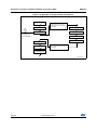
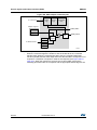
External interrupt/event controller (EXTI) . . . . . . . . . . . . . . . . . . . . . . . . 237
10.2.1
Main features . . . . . . . . . . . . . . . . . . . . . . . . . . . . . . . . . . . . . . . . . . . . 237
10.2.2
Block diagram . . . . . . . . . . . . . . . . . . . . . . . . . . . . . . . . . . . . . . . . . . . 237
10.2.3
Wakeup event management . . . . . . . . . . . . . . . . . . . . . . . . . . . . . . . . 238
10.2.4
Functional description . . . . . . . . . . . . . . . . . . . . . . . . . . . . . . . . . . . . . 238
10.2.5
External interrupt/event line mapping . . . . . . . . . . . . . . . . . . . . . . . . . 239
EXTI registers . . . . . . . . . . . . . . . . . . . . . . . . . . . . . . . . . . . . . . . . . . . . . 241
10.3.1
EXTI interrupt mask register (EXTI_IMR) . . . . . . . . . . . . . . . . . . . . . . 241
10.3.2
EXTI event mask register (EXTI_EMR) . . . . . . . . . . . . . . . . . . . . . . . . 241
10.3.3
EXTI rising edge trigger selection register (EXTI_RTSR) . . . . . . . . . . 242
10.3.4
Falling edge trigger selection register (EXTI_FTSR) . . . . . . . . . . . . . . 242
10.3.5
EXTI software interrupt event register (EXTI_SWIER) . . . . . . . . . . . . 243
10.3.6
EXTI pending register (EXTI_PR) . . . . . . . . . . . . . . . . . . . . . . . . . . . . 244
10.3.7
EXTI register map . . . . . . . . . . . . . . . . . . . . . . . . . . . . . . . . . . . . . . . . 244
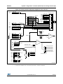
Direct memory access controller (DMA) . . . . . . . . . . . . . . . . . . . . . . . 246
11.1
DMA introduction . . . . . . . . . . . . . . . . . . . . . . . . . . . . . . . . . . . . . . . . . . 246
11.2
DMA main features . . . . . . . . . . . . . . . . . . . . . . . . . . . . . . . . . . . . . . . . . 246
11.3
DMA functional description . . . . . . . . . . . . . . . . . . . . . . . . . . . . . . . . . . . 249
11.4
8/901
9.3.1
Interrupts and events . . . . . . . . . . . . . . . . . . . . . . . . . . . . . . . . . . . . . . 230
10.1
11
Functional description . . . . . . . . . . . . . . . . . . . . . . . . . . . . . . . . . . . . . . 225
11.3.1
DMA transactions . . . . . . . . . . . . . . . . . . . . . . . . . . . . . . . . . . . . . . . . 249
11.3.2
Arbiter . . . . . . . . . . . . . . . . . . . . . . . . . . . . . . . . . . . . . . . . . . . . . . . . . 250
11.3.3
DMA channels . . . . . . . . . . . . . . . . . . . . . . . . . . . . . . . . . . . . . . . . . . . 250
11.3.4
Programmable data width, data alignment and endians . . . . . . . . . . . 252
11.3.5
Error management . . . . . . . . . . . . . . . . . . . . . . . . . . . . . . . . . . . . . . . . 253
11.3.6
Interrupts . . . . . . . . . . . . . . . . . . . . . . . . . . . . . . . . . . . . . . . . . . . . . . . 254
11.3.7
DMA request mapping . . . . . . . . . . . . . . . . . . . . . . . . . . . . . . . . . . . . . 254
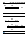
DMA registers . . . . . . . . . . . . . . . . . . . . . . . . . . . . . . . . . . . . . . . . . . . . . 257
DocID15965 Rev 13
RM0038
12
Contents
11.4.1
DMA interrupt status register (DMA_ISR) . . . . . . . . . . . . . . . . . . . . . . 258
11.4.2
DMA interrupt flag clear register (DMA_IFCR) . . . . . . . . . . . . . . . . . . 259
11.4.3
DMA channel x configuration register (DMA_CCRx) (x = 1..7,
where x = channel number) . . . . . . . . . . . . . . . . . . . . . . . . . . . . . . . . . 260
11.4.4
DMA channel x number of data register (DMA_CNDTRx) (x = 1..7),
where x = channel number) . . . . . . . . . . . . . . . . . . . . . . . . . . . . . . . . . 261
11.4.5
DMA channel x peripheral address register (DMA_CPARx) (x = 1..7),
where x = channel number) . . . . . . . . . . . . . . . . . . . . . . . . . . . . . . . . . 262
11.4.6
DMA channel x memory address register (DMA_CMARx) (x = 1..7),
where x = channel number) . . . . . . . . . . . . . . . . . . . . . . . . . . . . . . . . . 262
11.4.7
DMA register map . . . . . . . . . . . . . . . . . . . . . . . . . . . . . . . . . . . . . . . . 263
Analog-to-digital converter (ADC) . . . . . . . . . . . . . . . . . . . . . . . . . . . . 266
12.1
ADC introduction . . . . . . . . . . . . . . . . . . . . . . . . . . . . . . . . . . . . . . . . . . 266
12.2
ADC main features . . . . . . . . . . . . . . . . . . . . . . . . . . . . . . . . . . . . . . . . . 266
12.3
ADC functional description . . . . . . . . . . . . . . . . . . . . . . . . . . . . . . . . . . . 267
12.3.1
ADC power on-off control . . . . . . . . . . . . . . . . . . . . . . . . . . . . . . . . . . 270
12.3.2
ADC clock . . . . . . . . . . . . . . . . . . . . . . . . . . . . . . . . . . . . . . . . . . . . . . 270
12.3.3
Channel selection . . . . . . . . . . . . . . . . . . . . . . . . . . . . . . . . . . . . . . . . 271
12.3.4
Single conversion mode . . . . . . . . . . . . . . . . . . . . . . . . . . . . . . . . . . . 272
12.3.5
Continuous conversion mode . . . . . . . . . . . . . . . . . . . . . . . . . . . . . . . 272
12.3.6
Timing diagram . . . . . . . . . . . . . . . . . . . . . . . . . . . . . . . . . . . . . . . . . . 272
12.3.7
Analog watchdog . . . . . . . . . . . . . . . . . . . . . . . . . . . . . . . . . . . . . . . . . 273
12.3.8
Scan mode . . . . . . . . . . . . . . . . . . . . . . . . . . . . . . . . . . . . . . . . . . . . . . 274
12.3.9
Injected channel management . . . . . . . . . . . . . . . . . . . . . . . . . . . . . . . 274
12.3.10 Discontinuous mode . . . . . . . . . . . . . . . . . . . . . . . . . . . . . . . . . . . . . . 275
12.4
Data alignment . . . . . . . . . . . . . . . . . . . . . . . . . . . . . . . . . . . . . . . . . . . . 276
12.5
Channel-wise programmable sampling time . . . . . . . . . . . . . . . . . . . . . 277
12.6
Conversion on external trigger . . . . . . . . . . . . . . . . . . . . . . . . . . . . . . . . 278
12.7
Aborting a conversion . . . . . . . . . . . . . . . . . . . . . . . . . . . . . . . . . . . . . . . 279
12.7.1
Injected channels . . . . . . . . . . . . . . . . . . . . . . . . . . . . . . . . . . . . . . . . . 279
12.7.2
Regular channels . . . . . . . . . . . . . . . . . . . . . . . . . . . . . . . . . . . . . . . . . 280
12.8
Conversion resolution . . . . . . . . . . . . . . . . . . . . . . . . . . . . . . . . . . . . . . . 280
12.9
Hardware freeze and delay insertion modes for slow conversions . . . . 280
12.9.1
Inserting a delay after each regular conversion . . . . . . . . . . . . . . . . . . 281
12.9.2
Inserting a delay after each sequence of auto-injected conversions . . 282
12.10 Power saving . . . . . . . . . . . . . . . . . . . . . . . . . . . . . . . . . . . . . . . . . . . . . 283
DocID15965 Rev 13
9/901
26
Contents
RM0038
12.11 Data management and overrun detection . . . . . . . . . . . . . . . . . . . . . . . 285
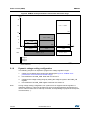
12.11.1 Using the DMA . . . . . . . . . . . . . . . . . . . . . . . . . . . . . . . . . . . . . . . . . . . 285
12.11.2 Managing a sequence of conversions without using the DMA . . . . . . 285
12.11.3 Conversions without reading all the data . . . . . . . . . . . . . . . . . . . . . . . 286
12.11.4 Overrun detection . . . . . . . . . . . . . . . . . . . . . . . . . . . . . . . . . . . . . . . . 286
12.12 Temperature sensor and internal reference voltage . . . . . . . . . . . . . . . . 286
12.13 Internal reference voltage (VREFINT) conversion . . . . . . . . . . . . . . . . . . 289
12.14 ADC interrupts . . . . . . . . . . . . . . . . . . . . . . . . . . . . . . . . . . . . . . . . . . . . 289
12.15 ADC registers . . . . . . . . . . . . . . . . . . . . . . . . . . . . . . . . . . . . . . . . . . . . . 290
12.15.1 ADC status register (ADC_SR) . . . . . . . . . . . . . . . . . . . . . . . . . . . . . . 290
12.15.2 ADC control register 1 (ADC_CR1) . . . . . . . . . . . . . . . . . . . . . . . . . . . 292
12.15.3 ADC control register 2 (ADC_CR2) . . . . . . . . . . . . . . . . . . . . . . . . . . . 294
12.15.4 ADC sample time register 1 (ADC_SMPR1) . . . . . . . . . . . . . . . . . . . . 298
12.15.5 ADC sample time register 2 (ADC_SMPR2) . . . . . . . . . . . . . . . . . . . . 298
12.15.6 ADC sample time register 3 (ADC_SMPR3) . . . . . . . . . . . . . . . . . . . . 299
12.15.7 ADC injected channel data offset register x (ADC_JOFRx)(x=1..4) . . 300
12.15.8 ADC watchdog higher threshold register (ADC_HTR) . . . . . . . . . . . . . 300
12.15.9 ADC watchdog lower threshold register (ADC_LTR) . . . . . . . . . . . . . . 300
12.15.10 ADC regular sequence register 1 (ADC_SQR1) . . . . . . . . . . . . . . . . . 301
12.15.11 ADC regular sequence register 2 (ADC_SQR2) . . . . . . . . . . . . . . . . . 301
12.15.12 ADC regular sequence register 3 (ADC_SQR3) . . . . . . . . . . . . . . . . . 302
12.15.13 ADC regular sequence register 4 (ADC_SQR4) . . . . . . . . . . . . . . . . . 303
12.15.14 ADC regular sequence register 5 (ADC_SQR5) . . . . . . . . . . . . . . . . . 303
12.15.15 ADC injected sequence register (ADC_JSQR) . . . . . . . . . . . . . . . . . . 304
12.15.16 ADC injected data register x (ADC_JDRx) (x= 1..4) . . . . . . . . . . . . . . 304
12.15.17 ADC regular data register (ADC_DR) . . . . . . . . . . . . . . . . . . . . . . . . . 305
12.15.18 ADC sample time register 0 (ADC_SMPR0) . . . . . . . . . . . . . . . . . . . . 305
12.15.19 ADC common status register (ADC_CSR) . . . . . . . . . . . . . . . . . . . . . 306
12.15.20 ADC common control register (ADC_CCR) . . . . . . . . . . . . . . . . . . . . . 306
12.15.21 ADC register map . . . . . . . . . . . . . . . . . . . . . . . . . . . . . . . . . . . . . . . . 308
13
Digital-to-analog converter (DAC) . . . . . . . . . . . . . . . . . . . . . . . . . . . . 311
13.1
DAC introduction . . . . . . . . . . . . . . . . . . . . . . . . . . . . . . . . . . . . . . . . . . .311
13.2
DAC main features . . . . . . . . . . . . . . . . . . . . . . . . . . . . . . . . . . . . . . . . . .311
13.3
DAC functional description . . . . . . . . . . . . . . . . . . . . . . . . . . . . . . . . . . . 313
13.3.1
10/901
DAC channel enable . . . . . . . . . . . . . . . . . . . . . . . . . . . . . . . . . . . . . . 313
DocID15965 Rev 13
RM0038
Contents
13.4
13.3.2
DAC output buffer enable . . . . . . . . . . . . . . . . . . . . . . . . . . . . . . . . . . 313
13.3.3
DAC data format . . . . . . . . . . . . . . . . . . . . . . . . . . . . . . . . . . . . . . . . . 313
13.3.4
DAC conversion . . . . . . . . . . . . . . . . . . . . . . . . . . . . . . . . . . . . . . . . . . 314
13.3.5
DAC output voltage . . . . . . . . . . . . . . . . . . . . . . . . . . . . . . . . . . . . . . . 315
13.3.6
DAC trigger selection . . . . . . . . . . . . . . . . . . . . . . . . . . . . . . . . . . . . . . 315
13.3.7
DMA request . . . . . . . . . . . . . . . . . . . . . . . . . . . . . . . . . . . . . . . . . . . . 316
13.3.8
Noise generation . . . . . . . . . . . . . . . . . . . . . . . . . . . . . . . . . . . . . . . . . 316
13.3.9
Triangle-wave generation . . . . . . . . . . . . . . . . . . . . . . . . . . . . . . . . . . 317
Dual DAC channel conversion . . . . . . . . . . . . . . . . . . . . . . . . . . . . . . . . 318
13.4.1
Independent trigger without wave generation . . . . . . . . . . . . . . . . . . . 318
13.4.2
Independent trigger with single LFSR generation . . . . . . . . . . . . . . . . 319
13.4.3
Independent trigger with different LFSR generation . . . . . . . . . . . . . . 319
13.4.4
Independent trigger with single triangle generation . . . . . . . . . . . . . . . 320
13.4.5
Independent trigger with different triangle generation . . . . . . . . . . . . . 320
13.4.6
Simultaneous software start . . . . . . . . . . . . . . . . . . . . . . . . . . . . . . . . . 320
13.4.7
Simultaneous trigger without wave generation . . . . . . . . . . . . . . . . . . 321
13.4.8
Simultaneous trigger with single LFSR generation . . . . . . . . . . . . . . . 321
13.4.9
Simultaneous trigger with different LFSR generation . . . . . . . . . . . . . 321
13.4.10 Simultaneous trigger with single triangle generation . . . . . . . . . . . . . . 322
13.4.11 Simultaneous trigger with different triangle generation . . . . . . . . . . . . 322
13.5
DAC registers . . . . . . . . . . . . . . . . . . . . . . . . . . . . . . . . . . . . . . . . . . . . . 323
13.5.1
DAC control register (DAC_CR) . . . . . . . . . . . . . . . . . . . . . . . . . . . . . 323
13.5.2
DAC software trigger register (DAC_SWTRIGR) . . . . . . . . . . . . . . . . . 326
13.5.3
DAC channel1 12-bit right-aligned data holding register
(DAC_DHR12R1) . . . . . . . . . . . . . . . . . . . . . . . . . . . . . . . . . . . . . . . . 326
13.5.4
DAC channel1 12-bit left aligned data holding register
(DAC_DHR12L1) . . . . . . . . . . . . . . . . . . . . . . . . . . . . . . . . . . . . . . . . . 327
13.5.5
DAC channel1 8-bit right aligned data holding register
(DAC_DHR8R1) . . . . . . . . . . . . . . . . . . . . . . . . . . . . . . . . . . . . . . . . . 327
13.5.6
DAC channel2 12-bit right aligned data holding register
(DAC_DHR12R2) . . . . . . . . . . . . . . . . . . . . . . . . . . . . . . . . . . . . . . . . 328
13.5.7
DAC channel2 12-bit left aligned data holding register
(DAC_DHR12L2) . . . . . . . . . . . . . . . . . . . . . . . . . . . . . . . . . . . . . . . . . 328
13.5.8
DAC channel2 8-bit right-aligned data holding register
(DAC_DHR8R2) . . . . . . . . . . . . . . . . . . . . . . . . . . . . . . . . . . . . . . . . . 328
13.5.9
Dual DAC 12-bit right-aligned data holding register
(DAC_DHR12RD) . . . . . . . . . . . . . . . . . . . . . . . . . . . . . . . . . . . . . . . . 329
13.5.10 DUAL DAC 12-bit left aligned data holding register
(DAC_DHR12LD) . . . . . . . . . . . . . . . . . . . . . . . . . . . . . . . . . . . . . . . . 329
DocID15965 Rev 13
11/901
26
Contents
RM0038
13.5.11 DUAL DAC 8-bit right aligned data holding register
(DAC_DHR8RD) . . . . . . . . . . . . . . . . . . . . . . . . . . . . . . . . . . . . . . . . . 330
13.5.12 DAC channel1 data output register (DAC_DOR1) . . . . . . . . . . . . . . . . 330
13.5.13 DAC channel2 data output register (DAC_DOR2) . . . . . . . . . . . . . . . . 330
13.5.14 DAC status register (DAC_SR) . . . . . . . . . . . . . . . . . . . . . . . . . . . . . . 331
13.5.15 DAC register map . . . . . . . . . . . . . . . . . . . . . . . . . . . . . . . . . . . . . . . . 331
14
15
Comparators (COMP) . . . . . . . . . . . . . . . . . . . . . . . . . . . . . . . . . . . . . . 333
14.1
Introduction . . . . . . . . . . . . . . . . . . . . . . . . . . . . . . . . . . . . . . . . . . . . . . 333
14.2
Main features . . . . . . . . . . . . . . . . . . . . . . . . . . . . . . . . . . . . . . . . . . . . . 333
14.3
COMP clock . . . . . . . . . . . . . . . . . . . . . . . . . . . . . . . . . . . . . . . . . . . . . . 333
14.4
Comparator 1 (COMP1) . . . . . . . . . . . . . . . . . . . . . . . . . . . . . . . . . . . . . 334
14.5
Comparator 2 (COMP2) . . . . . . . . . . . . . . . . . . . . . . . . . . . . . . . . . . . . . 337
14.6
Comparators in Window mode . . . . . . . . . . . . . . . . . . . . . . . . . . . . . . . . 339
14.7
Low power modes . . . . . . . . . . . . . . . . . . . . . . . . . . . . . . . . . . . . . . . . . 339
14.8
Interrupts . . . . . . . . . . . . . . . . . . . . . . . . . . . . . . . . . . . . . . . . . . . . . . . . 340
14.9
COMP registers . . . . . . . . . . . . . . . . . . . . . . . . . . . . . . . . . . . . . . . . . . . 340
14.9.2
COMP register map . . . . . . . . . . . . . . . . . . . . . . . . . . . . . . . . . . . . . . . 343
15.1
OPAMP introduction . . . . . . . . . . . . . . . . . . . . . . . . . . . . . . . . . . . . . . . . 344
15.2
OPAMP main features . . . . . . . . . . . . . . . . . . . . . . . . . . . . . . . . . . . . . . 344
15.3
OPAMP functional description . . . . . . . . . . . . . . . . . . . . . . . . . . . . . . . . 344
15.3.1
Signal routing . . . . . . . . . . . . . . . . . . . . . . . . . . . . . . . . . . . . . . . . . . . . 345
15.3.2
Using the OPAMP outputs as ADC inputs . . . . . . . . . . . . . . . . . . . . . . 346
15.3.3
Calibration . . . . . . . . . . . . . . . . . . . . . . . . . . . . . . . . . . . . . . . . . . . . . . 346
OPAMP registers . . . . . . . . . . . . . . . . . . . . . . . . . . . . . . . . . . . . . . . . . . 348
15.4.1
OPAMP control/status register (OPAMP_CSR) . . . . . . . . . . . . . . . . . . 348
15.4.2
OPAMP offset trimming register for normal mode (OPAMP_OTR) . . . 351
15.4.3
OPAMP offset trimming register for low power mode
(OPAMP_LPOTR) . . . . . . . . . . . . . . . . . . . . . . . . . . . . . . . . . . . . . . . . 352
15.4.4
OPAMP register map . . . . . . . . . . . . . . . . . . . . . . . . . . . . . . . . . . . . . . 353
Liquid crystal display controller (LCD) . . . . . . . . . . . . . . . . . . . . . . . . 354
16.1
12/901
COMP comparator control and status register (COMP_CSR) . . . . . . . 340
Operational amplifiers (OPAMP) . . . . . . . . . . . . . . . . . . . . . . . . . . . . . 344
15.4
16
14.9.1
Introduction . . . . . . . . . . . . . . . . . . . . . . . . . . . . . . . . . . . . . . . . . . . . . . 354
DocID15965 Rev 13
RM0038
Contents
16.2
LCD main features . . . . . . . . . . . . . . . . . . . . . . . . . . . . . . . . . . . . . . . . . 355
16.3
Glossary . . . . . . . . . . . . . . . . . . . . . . . . . . . . . . . . . . . . . . . . . . . . . . . . . 356
16.4
LCD functional description . . . . . . . . . . . . . . . . . . . . . . . . . . . . . . . . . . . 357
16.5
17
16.4.1
General description . . . . . . . . . . . . . . . . . . . . . . . . . . . . . . . . . . . . . . . 357
16.4.2
Frequency generator . . . . . . . . . . . . . . . . . . . . . . . . . . . . . . . . . . . . . . 358
16.4.3
Common driver . . . . . . . . . . . . . . . . . . . . . . . . . . . . . . . . . . . . . . . . . . 359
16.4.4
Segment driver . . . . . . . . . . . . . . . . . . . . . . . . . . . . . . . . . . . . . . . . . . 362
16.4.5
Voltage generator . . . . . . . . . . . . . . . . . . . . . . . . . . . . . . . . . . . . . . . . 367
16.4.6
Deadtime . . . . . . . . . . . . . . . . . . . . . . . . . . . . . . . . . . . . . . . . . . . . . . . 369
16.4.7
Double buffer memory . . . . . . . . . . . . . . . . . . . . . . . . . . . . . . . . . . . . . 370
16.4.8
COM and SEG multiplexing . . . . . . . . . . . . . . . . . . . . . . . . . . . . . . . . . 370
16.4.9
Flowchart . . . . . . . . . . . . . . . . . . . . . . . . . . . . . . . . . . . . . . . . . . . . . . . 374
LCD registers . . . . . . . . . . . . . . . . . . . . . . . . . . . . . . . . . . . . . . . . . . . . . 375
16.5.1
LCD control register (LCD_CR) . . . . . . . . . . . . . . . . . . . . . . . . . . . . . . 375
16.5.2
LCD frame control register (LCD_FCR) . . . . . . . . . . . . . . . . . . . . . . . . 376
16.5.3
LCD status register (LCD_SR) . . . . . . . . . . . . . . . . . . . . . . . . . . . . . . 378
16.5.4
LCD clear register (LCD_CLR) . . . . . . . . . . . . . . . . . . . . . . . . . . . . . . 379
16.5.5
LCD display memory (LCD_RAM) . . . . . . . . . . . . . . . . . . . . . . . . . . . . 380
16.5.6
LCD register map . . . . . . . . . . . . . . . . . . . . . . . . . . . . . . . . . . . . . . . . . 380
General-purpose timers (TIM2 to TIM5) . . . . . . . . . . . . . . . . . . . . . . . . 383
17.1
TIM2 to TIM5 introduction . . . . . . . . . . . . . . . . . . . . . . . . . . . . . . . . . . . 383
17.2
TIM2 to TIM5 main features . . . . . . . . . . . . . . . . . . . . . . . . . . . . . . . . . . 383
17.3
TIM2 to TIM5 functional description . . . . . . . . . . . . . . . . . . . . . . . . . . . . 384
17.3.1
Time-base unit . . . . . . . . . . . . . . . . . . . . . . . . . . . . . . . . . . . . . . . . . . . 384
17.3.2
Counter modes . . . . . . . . . . . . . . . . . . . . . . . . . . . . . . . . . . . . . . . . . . 386
17.3.3
Clock selection . . . . . . . . . . . . . . . . . . . . . . . . . . . . . . . . . . . . . . . . . . . 394
17.3.4
Capture/compare channels . . . . . . . . . . . . . . . . . . . . . . . . . . . . . . . . . 397
17.3.5
Input capture mode . . . . . . . . . . . . . . . . . . . . . . . . . . . . . . . . . . . . . . . 399
17.3.6
PWM input mode . . . . . . . . . . . . . . . . . . . . . . . . . . . . . . . . . . . . . . . . . 400
17.3.7
Forced output mode . . . . . . . . . . . . . . . . . . . . . . . . . . . . . . . . . . . . . . . 401
17.3.8
Output compare mode . . . . . . . . . . . . . . . . . . . . . . . . . . . . . . . . . . . . . 402
17.3.9
PWM mode . . . . . . . . . . . . . . . . . . . . . . . . . . . . . . . . . . . . . . . . . . . . . 403
17.3.10 One-pulse mode . . . . . . . . . . . . . . . . . . . . . . . . . . . . . . . . . . . . . . . . . 406
17.3.11 Clearing the OCxREF signal on an external event . . . . . . . . . . . . . . . 407
17.3.12 Encoder interface mode . . . . . . . . . . . . . . . . . . . . . . . . . . . . . . . . . . . . 408
DocID15965 Rev 13
13/901
26
Contents
RM0038
17.3.13 Timer input XOR function . . . . . . . . . . . . . . . . . . . . . . . . . . . . . . . . . . . 410
17.3.14 Timers and external trigger synchronization . . . . . . . . . . . . . . . . . . . . 410
17.3.15 Timer synchronization . . . . . . . . . . . . . . . . . . . . . . . . . . . . . . . . . . . . . 413
17.3.16 Debug mode . . . . . . . . . . . . . . . . . . . . . . . . . . . . . . . . . . . . . . . . . . . . 418
17.4
TIMx registers . . . . . . . . . . . . . . . . . . . . . . . . . . . . . . . . . . . . . . . . . . . . . 419
17.4.1
TIMx control register 1 (TIMx_CR1) . . . . . . . . . . . . . . . . . . . . . . . . . . 419
17.4.2
TIMx control register 2 (TIMx_CR2) . . . . . . . . . . . . . . . . . . . . . . . . . . 421
17.4.3
TIMx slave mode control register (TIMx_SMCR) . . . . . . . . . . . . . . . . . 422
17.4.4
TIMx DMA/Interrupt enable register (TIMx_DIER) . . . . . . . . . . . . . . . . 424
17.4.5
TIMx status register (TIMx_SR) . . . . . . . . . . . . . . . . . . . . . . . . . . . . . . 425
17.4.6
TIMx event generation register (TIMx_EGR) . . . . . . . . . . . . . . . . . . . . 427
17.4.7
TIMx capture/compare mode register 1 (TIMx_CCMR1) . . . . . . . . . . . 428
17.4.8
TIMx capture/compare mode register 2 (TIMx_CCMR2) . . . . . . . . . . . 431
17.4.9
TIMx capture/compare enable register (TIMx_CCER) . . . . . . . . . . . . . 432
17.4.10 TIMx counter (TIMx_CNT) . . . . . . . . . . . . . . . . . . . . . . . . . . . . . . . . . . 434
17.4.11 TIMx prescaler (TIMx_PSC) . . . . . . . . . . . . . . . . . . . . . . . . . . . . . . . . 434
17.4.12 TIMx auto-reload register (TIMx_ARR) . . . . . . . . . . . . . . . . . . . . . . . . 434
17.4.13 TIMx capture/compare register 1 (TIMx_CCR1) . . . . . . . . . . . . . . . . . 434
17.4.14 TIMx capture/compare register 2 (TIMx_CCR2) . . . . . . . . . . . . . . . . . 435
17.4.15 TIMx capture/compare register 3 (TIMx_CCR3) . . . . . . . . . . . . . . . . . 435
17.4.16 TIMx capture/compare register 4 (TIMx_CCR4) . . . . . . . . . . . . . . . . . 436
17.4.17 TIMx DMA control register (TIMx_DCR) . . . . . . . . . . . . . . . . . . . . . . . 436
17.4.18 TIMx DMA address for full transfer (TIMx_DMAR) . . . . . . . . . . . . . . . 437
17.4.19 TIM2 option register (TIM2_OR) . . . . . . . . . . . . . . . . . . . . . . . . . . . . . 437
17.4.20 TIM3 option register (TIM3_OR) . . . . . . . . . . . . . . . . . . . . . . . . . . . . . 438
17.4.21 TIMx register map . . . . . . . . . . . . . . . . . . . . . . . . . . . . . . . . . . . . . . . . 439
18
General-purpose timers (TIM9/10/11) . . . . . . . . . . . . . . . . . . . . . . . . . 442
18.1
TIM9/10/11 introduction . . . . . . . . . . . . . . . . . . . . . . . . . . . . . . . . . . . . . 442
18.2
TIM9/10/11 main features . . . . . . . . . . . . . . . . . . . . . . . . . . . . . . . . . . . . 442
18.3
14/901
18.2.1
TIM9 main features . . . . . . . . . . . . . . . . . . . . . . . . . . . . . . . . . . . . . . . 442
18.2.2
TIM10/TIM11 main features . . . . . . . . . . . . . . . . . . . . . . . . . . . . . . . . . 443
TIM9/10/11 functional description . . . . . . . . . . . . . . . . . . . . . . . . . . . . . . 446
18.3.1
Time-base unit . . . . . . . . . . . . . . . . . . . . . . . . . . . . . . . . . . . . . . . . . . . 446
18.3.2
Counter modes . . . . . . . . . . . . . . . . . . . . . . . . . . . . . . . . . . . . . . . . . . 447
18.3.3
Clock selection . . . . . . . . . . . . . . . . . . . . . . . . . . . . . . . . . . . . . . . . . . . 450
18.3.4
Capture/compare channels . . . . . . . . . . . . . . . . . . . . . . . . . . . . . . . . . 452
DocID15965 Rev 13
RM0038
Contents
18.3.5
Input capture mode . . . . . . . . . . . . . . . . . . . . . . . . . . . . . . . . . . . . . . . 453
18.3.6
PWM input mode (only for TIM9) . . . . . . . . . . . . . . . . . . . . . . . . . . . . . 455
18.3.7
Forced output mode . . . . . . . . . . . . . . . . . . . . . . . . . . . . . . . . . . . . . . . 456
18.3.8
Output compare mode . . . . . . . . . . . . . . . . . . . . . . . . . . . . . . . . . . . . . 456
18.3.9
PWM mode . . . . . . . . . . . . . . . . . . . . . . . . . . . . . . . . . . . . . . . . . . . . . 457
18.3.10 One-pulse mode . . . . . . . . . . . . . . . . . . . . . . . . . . . . . . . . . . . . . . . . . 458
18.3.11 TIM9 external trigger synchronization . . . . . . . . . . . . . . . . . . . . . . . . . 460
18.3.12 Timer synchronization (TIM9) . . . . . . . . . . . . . . . . . . . . . . . . . . . . . . . 462
18.3.13 Debug mode . . . . . . . . . . . . . . . . . . . . . . . . . . . . . . . . . . . . . . . . . . . . 462
18.3.14 Encoder interface mode (only for TIM9) . . . . . . . . . . . . . . . . . . . . . . . 462
18.4
TIM9 registers . . . . . . . . . . . . . . . . . . . . . . . . . . . . . . . . . . . . . . . . . . . . 463
18.4.1
TIM9 control register 1 (TIMx_CR1) . . . . . . . . . . . . . . . . . . . . . . . . . . 463
18.4.2
TIM9 control register 2 (TIMx_CR2) . . . . . . . . . . . . . . . . . . . . . . . . . . 465
18.4.3
TIM9 slave mode control register (TIMx_SMCR) . . . . . . . . . . . . . . . . 466
18.4.4
TIM9 Interrupt enable register (TIMx_DIER) . . . . . . . . . . . . . . . . . . . . 468
18.4.5
TIM9 status register (TIMx_SR) . . . . . . . . . . . . . . . . . . . . . . . . . . . . . . 470
18.4.6
TIM event generation register (TIMx_EGR) . . . . . . . . . . . . . . . . . . . . . 471
18.4.7
TIM capture/compare mode register 1 (TIMx_CCMR1) . . . . . . . . . . . . 473
18.4.8
TIM9 capture/compare enable register (TIMx_CCER) . . . . . . . . . . . . 476
18.4.9
TIM9 counter (TIMx_CNT) . . . . . . . . . . . . . . . . . . . . . . . . . . . . . . . . . . 477
18.4.10 TIM9 prescaler (TIMx_PSC) . . . . . . . . . . . . . . . . . . . . . . . . . . . . . . . . 477
18.4.11 TIM9 auto-reload register (TIMx_ARR) . . . . . . . . . . . . . . . . . . . . . . . . 477
18.4.12 TIM9 capture/compare register 1 (TIMx_CCR1) . . . . . . . . . . . . . . . . . 478
18.4.13 TIM9 capture/compare register 2 (TIMx_CCR2) . . . . . . . . . . . . . . . . . 478
18.4.14 TIM9 option register 1 (TIM9_OR) . . . . . . . . . . . . . . . . . . . . . . . . . . . . 479
18.4.15 TIM9 register map . . . . . . . . . . . . . . . . . . . . . . . . . . . . . . . . . . . . . . . . 479
18.5
TIM10/11 registers . . . . . . . . . . . . . . . . . . . . . . . . . . . . . . . . . . . . . . . . . 481
18.5.1
TIM10/11 control register 1 (TIMx_CR1) . . . . . . . . . . . . . . . . . . . . . . . 481
18.5.2
TIM10/11 slave mode control register 1 (TIMx_SMCR) . . . . . . . . . . . . 482
18.5.3
TIM10/11 Interrupt enable register (TIMx_DIER) . . . . . . . . . . . . . . . . . 484
18.5.4
TIM10/11 status register (TIMx_SR) . . . . . . . . . . . . . . . . . . . . . . . . . . 484
18.5.5
TIM10/11 event generation register (TIMx_EGR) . . . . . . . . . . . . . . . . 485
18.5.6
TIM10/11 capture/compare mode register 1
(TIMx_CCMR1) . . . . . . . . . . . . . . . . . . . . . . . . . . . . . . . . . . . . . . . . . . 486
18.5.7
TIM10/11 capture/compare enable register
(TIMx_CCER) . . . . . . . . . . . . . . . . . . . . . . . . . . . . . . . . . . . . . . . . . . . 489
18.5.8
TIM10/11 counter (TIMx_CNT) . . . . . . . . . . . . . . . . . . . . . . . . . . . . . . 490
DocID15965 Rev 13
15/901
26
Contents
RM0038
18.5.9
TIM10/11 prescaler (TIMx_PSC) . . . . . . . . . . . . . . . . . . . . . . . . . . . . . 490
18.5.10 TIM10/11 auto-reload register (TIMx_ARR) . . . . . . . . . . . . . . . . . . . . . 490
18.5.11 TIM10/11 capture/compare register 1 (TIMx_CCR1) . . . . . . . . . . . . . . 491
18.5.12 TIM10 option register 1 (TIM10_OR) . . . . . . . . . . . . . . . . . . . . . . . . . . 491
18.5.13 TIM11 option register 1 (TIM11_OR) . . . . . . . . . . . . . . . . . . . . . . . . . . 492
18.5.14 TIM10/11 register map . . . . . . . . . . . . . . . . . . . . . . . . . . . . . . . . . . . . . 493
19
Basic timers (TIM6&TIM7) . . . . . . . . . . . . . . . . . . . . . . . . . . . . . . . . . . . 495
19.1
TIM6&TIM7 introduction . . . . . . . . . . . . . . . . . . . . . . . . . . . . . . . . . . . . . 495
19.2
TIM6&TIM7 main features . . . . . . . . . . . . . . . . . . . . . . . . . . . . . . . . . . . 495
19.3
TIM6&TIM7 functional description . . . . . . . . . . . . . . . . . . . . . . . . . . . . . 496
19.4
20
16/901
19.3.1
Time-base unit . . . . . . . . . . . . . . . . . . . . . . . . . . . . . . . . . . . . . . . . . . . 496
19.3.2
Counting mode . . . . . . . . . . . . . . . . . . . . . . . . . . . . . . . . . . . . . . . . . . 497
19.3.3
Clock source . . . . . . . . . . . . . . . . . . . . . . . . . . . . . . . . . . . . . . . . . . . . 500
19.3.4
Debug mode . . . . . . . . . . . . . . . . . . . . . . . . . . . . . . . . . . . . . . . . . . . . 500
TIM6&TIM7 registers . . . . . . . . . . . . . . . . . . . . . . . . . . . . . . . . . . . . . . . 501
19.4.1
TIM6&TIM7 control register 1 (TIMx_CR1) . . . . . . . . . . . . . . . . . . . . . 501
19.4.2
TIM6&TIM7 control register 2 (TIMx_CR2) . . . . . . . . . . . . . . . . . . . . . 502
19.4.3
TIM6&TIM7 DMA/Interrupt enable register (TIMx_DIER) . . . . . . . . . . 502
19.4.4
TIM6&TIM7 status register (TIMx_SR) . . . . . . . . . . . . . . . . . . . . . . . . 503
19.4.5
TIM6&TIM7 event generation register (TIMx_EGR) . . . . . . . . . . . . . . 503
19.4.6
TIM6&TIM7 counter (TIMx_CNT) . . . . . . . . . . . . . . . . . . . . . . . . . . . . 503
19.4.7
TIM6&TIM7 prescaler (TIMx_PSC) . . . . . . . . . . . . . . . . . . . . . . . . . . . 504
19.4.8
TIM6&TIM7 auto-reload register (TIMx_ARR) . . . . . . . . . . . . . . . . . . . 504
19.4.9
TIM6&TIM7 register map . . . . . . . . . . . . . . . . . . . . . . . . . . . . . . . . . . . 505
Real-time clock (RTC) . . . . . . . . . . . . . . . . . . . . . . . . . . . . . . . . . . . . . . 506
20.1
Introduction . . . . . . . . . . . . . . . . . . . . . . . . . . . . . . . . . . . . . . . . . . . . . . 506
20.2
RTC main features . . . . . . . . . . . . . . . . . . . . . . . . . . . . . . . . . . . . . . . . . 507
20.3
RTC functional description . . . . . . . . . . . . . . . . . . . . . . . . . . . . . . . . . . . 509
20.3.1
Clock and prescalers . . . . . . . . . . . . . . . . . . . . . . . . . . . . . . . . . . . . . . 509
20.3.2
Real-time clock and calendar . . . . . . . . . . . . . . . . . . . . . . . . . . . . . . . 510
20.3.3
Programmable alarms . . . . . . . . . . . . . . . . . . . . . . . . . . . . . . . . . . . . . 510
20.3.4
Periodic auto-wakeup . . . . . . . . . . . . . . . . . . . . . . . . . . . . . . . . . . . . . 511
20.3.5
RTC initialization and configuration . . . . . . . . . . . . . . . . . . . . . . . . . . . 512
20.3.6
Reading the calendar . . . . . . . . . . . . . . . . . . . . . . . . . . . . . . . . . . . . . . 513
DocID15965 Rev 13
RM0038
Contents
20.3.7
Resetting the RTC . . . . . . . . . . . . . . . . . . . . . . . . . . . . . . . . . . . . . . . . 514
20.3.8
RTC synchronization (Cat.2, Cat.3, Cat.4, Cat.5 and Cat.6
devices only) . . . . . . . . . . . . . . . . . . . . . . . . . . . . . . . . . . . . . . . . . . . . 515
20.3.9
RTC reference clock detection . . . . . . . . . . . . . . . . . . . . . . . . . . . . . . 515
20.3.10 RTC coarse digital calibration . . . . . . . . . . . . . . . . . . . . . . . . . . . . . . . 516
20.3.11 RTC smooth digital calibration (Cat.2, Cat.3, Cat.4, Cat.5 and Cat.6
devices only) . . . . . . . . . . . . . . . . . . . . . . . . . . . . . . . . . . . . . . . . . . . . 517
20.3.12 Timestamp function . . . . . . . . . . . . . . . . . . . . . . . . . . . . . . . . . . . . . . . 519
20.3.13 Tamper detection . . . . . . . . . . . . . . . . . . . . . . . . . . . . . . . . . . . . . . . . . 520
20.3.14 Calibration clock output . . . . . . . . . . . . . . . . . . . . . . . . . . . . . . . . . . . . 521
20.3.15 Alarm output . . . . . . . . . . . . . . . . . . . . . . . . . . . . . . . . . . . . . . . . . . . . 522
20.4
RTC and low-power modes . . . . . . . . . . . . . . . . . . . . . . . . . . . . . . . . . . 522
20.5
RTC interrupts . . . . . . . . . . . . . . . . . . . . . . . . . . . . . . . . . . . . . . . . . . . . 522
20.6
RTC registers . . . . . . . . . . . . . . . . . . . . . . . . . . . . . . . . . . . . . . . . . . . . . 524
20.6.1
RTC time register (RTC_TR) . . . . . . . . . . . . . . . . . . . . . . . . . . . . . . . . 524
20.6.2
RTC date register (RTC_DR) . . . . . . . . . . . . . . . . . . . . . . . . . . . . . . . . 525
20.6.3
RTC control register (RTC_CR) . . . . . . . . . . . . . . . . . . . . . . . . . . . . . . 526
20.6.4
RTC initialization and status register (RTC_ISR) . . . . . . . . . . . . . . . . . 528
20.6.5
RTC prescaler register (RTC_PRER) . . . . . . . . . . . . . . . . . . . . . . . . . 531
20.6.6
RTC wakeup timer register (RTC_WUTR) . . . . . . . . . . . . . . . . . . . . . . 531
20.6.7
RTC calibration register (RTC_CALIBR) . . . . . . . . . . . . . . . . . . . . . . . 532
20.6.8
RTC alarm A register (RTC_ALRMAR) . . . . . . . . . . . . . . . . . . . . . . . . 533
20.6.9
RTC alarm B register (RTC_ALRMBR) . . . . . . . . . . . . . . . . . . . . . . . . 534
20.6.10 RTC write protection register (RTC_WPR) . . . . . . . . . . . . . . . . . . . . . 535
20.6.11 RTC sub second register (RTC_SSR) . . . . . . . . . . . . . . . . . . . . . . . . . 535
20.6.12 RTC shift control register (RTC_SHIFTR) . . . . . . . . . . . . . . . . . . . . . . 536
20.6.13 RTC time stamp time register (RTC_TSTR) . . . . . . . . . . . . . . . . . . . . 537
20.6.14 RTC time stamp date register (RTC_TSDR) . . . . . . . . . . . . . . . . . . . . 537
20.6.15 RTC timestamp sub second register (RTC_TSSSR) . . . . . . . . . . . . . . 538
20.6.16 RTC calibration register (RTC_CALR) . . . . . . . . . . . . . . . . . . . . . . . . . 538
20.6.17 RTC tamper and alternate function configuration register
(RTC_TAFCR) . . . . . . . . . . . . . . . . . . . . . . . . . . . . . . . . . . . . . . . . . . . 540
20.6.18 RTC alarm A sub second register (RTC_ALRMASSR) . . . . . . . . . . . . 542
20.6.19 RTC alarm B sub second register (RTC_ALRMBSSR) . . . . . . . . . . . . 543
20.6.20 RTC backup registers (RTC_BKPxR) . . . . . . . . . . . . . . . . . . . . . . . . . 544
20.6.21 RTC register map . . . . . . . . . . . . . . . . . . . . . . . . . . . . . . . . . . . . . . . . 544
21
Independent watchdog (IWDG) . . . . . . . . . . . . . . . . . . . . . . . . . . . . . . 547
DocID15965 Rev 13
17/901
26
Contents
RM0038
21.1
IWDG introduction . . . . . . . . . . . . . . . . . . . . . . . . . . . . . . . . . . . . . . . . . 547
21.2
IWDG main features . . . . . . . . . . . . . . . . . . . . . . . . . . . . . . . . . . . . . . . . 547
21.3
IWDG functional description . . . . . . . . . . . . . . . . . . . . . . . . . . . . . . . . . . 547
21.4
22
23
Hardware watchdog . . . . . . . . . . . . . . . . . . . . . . . . . . . . . . . . . . . . . . . 547
21.3.2
Register access protection . . . . . . . . . . . . . . . . . . . . . . . . . . . . . . . . . 547
21.3.3
Debug mode . . . . . . . . . . . . . . . . . . . . . . . . . . . . . . . . . . . . . . . . . . . . 548
IWDG registers . . . . . . . . . . . . . . . . . . . . . . . . . . . . . . . . . . . . . . . . . . . . 549
21.4.1
Key register (IWDG_KR) . . . . . . . . . . . . . . . . . . . . . . . . . . . . . . . . . . . 549
21.4.2
Prescaler register (IWDG_PR) . . . . . . . . . . . . . . . . . . . . . . . . . . . . . . 549
21.4.3
Reload register (IWDG_RLR) . . . . . . . . . . . . . . . . . . . . . . . . . . . . . . . 550
21.4.4
Status register (IWDG_SR) . . . . . . . . . . . . . . . . . . . . . . . . . . . . . . . . . 550
21.4.5
IWDG register map . . . . . . . . . . . . . . . . . . . . . . . . . . . . . . . . . . . . . . . 551
Window watchdog (WWDG) . . . . . . . . . . . . . . . . . . . . . . . . . . . . . . . . . 552
22.1
WWDG introduction . . . . . . . . . . . . . . . . . . . . . . . . . . . . . . . . . . . . . . . . 552
22.2
WWDG main features . . . . . . . . . . . . . . . . . . . . . . . . . . . . . . . . . . . . . . 552
22.3
WWDG functional description . . . . . . . . . . . . . . . . . . . . . . . . . . . . . . . . 552
22.4
How to program the watchdog timeout . . . . . . . . . . . . . . . . . . . . . . . . . . 554
22.5
Debug mode . . . . . . . . . . . . . . . . . . . . . . . . . . . . . . . . . . . . . . . . . . . . . . 555
22.6
WWDG registers . . . . . . . . . . . . . . . . . . . . . . . . . . . . . . . . . . . . . . . . . . 556
22.6.1
Control register (WWDG_CR) . . . . . . . . . . . . . . . . . . . . . . . . . . . . . . . 556
22.6.2
Configuration register (WWDG_CFR) . . . . . . . . . . . . . . . . . . . . . . . . . 557
22.6.3
Status register (WWDG_SR) . . . . . . . . . . . . . . . . . . . . . . . . . . . . . . . . 557
22.6.4
WWDG register map . . . . . . . . . . . . . . . . . . . . . . . . . . . . . . . . . . . . . . 558
Advanced encryption standard hardware accelerator (AES) . . . . . . 559
23.1
Introduction . . . . . . . . . . . . . . . . . . . . . . . . . . . . . . . . . . . . . . . . . . . . . . 559
23.2
AES main features . . . . . . . . . . . . . . . . . . . . . . . . . . . . . . . . . . . . . . . . . 559
23.3
AES functional description . . . . . . . . . . . . . . . . . . . . . . . . . . . . . . . . . . . 560
23.4
Encryption and derivation keys . . . . . . . . . . . . . . . . . . . . . . . . . . . . . . . 561
23.5
AES chaining algorithms . . . . . . . . . . . . . . . . . . . . . . . . . . . . . . . . . . . . 562
23.6
18/901
21.3.1
23.5.1
Electronic CodeBook (ECB) . . . . . . . . . . . . . . . . . . . . . . . . . . . . . . . . 562
23.5.2
Cipher block chaining (CBC) . . . . . . . . . . . . . . . . . . . . . . . . . . . . . . . . 563
23.5.3
Counter Mode (CTR) . . . . . . . . . . . . . . . . . . . . . . . . . . . . . . . . . . . . . . 567
Data type . . . . . . . . . . . . . . . . . . . . . . . . . . . . . . . . . . . . . . . . . . . . . . . . 568
DocID15965 Rev 13
RM0038
Contents
23.7
Operating modes . . . . . . . . . . . . . . . . . . . . . . . . . . . . . . . . . . . . . . . . . . 571
23.7.1
Mode 1: encryption . . . . . . . . . . . . . . . . . . . . . . . . . . . . . . . . . . . . . . . 571
23.7.2
Mode 2: key derivation . . . . . . . . . . . . . . . . . . . . . . . . . . . . . . . . . . . . . 572
23.7.3
Mode 3: decryption . . . . . . . . . . . . . . . . . . . . . . . . . . . . . . . . . . . . . . . 572
23.7.4
Mode 4: key derivation and decryption . . . . . . . . . . . . . . . . . . . . . . . . 573
23.8
AES DMA interface . . . . . . . . . . . . . . . . . . . . . . . . . . . . . . . . . . . . . . . . 573
23.9
Error flags . . . . . . . . . . . . . . . . . . . . . . . . . . . . . . . . . . . . . . . . . . . . . . . . 575
23.10 Processing time . . . . . . . . . . . . . . . . . . . . . . . . . . . . . . . . . . . . . . . . . . . 575
23.11 AES interrupts . . . . . . . . . . . . . . . . . . . . . . . . . . . . . . . . . . . . . . . . . . . . 575
23.12 AES registers . . . . . . . . . . . . . . . . . . . . . . . . . . . . . . . . . . . . . . . . . . . . . 576
23.12.1 AES control register (AES_CR) . . . . . . . . . . . . . . . . . . . . . . . . . . . . . . 576
23.12.2 AES status register (AES_SR) . . . . . . . . . . . . . . . . . . . . . . . . . . . . . . 578
23.12.3 AES data input register (AES_DINR) . . . . . . . . . . . . . . . . . . . . . . . . . 579
23.12.4 AES data output register (AES_DOUTR) . . . . . . . . . . . . . . . . . . . . . . 579
23.12.5 AES key register 0(AES_KEYR0) (LSB: key [31:0]) . . . . . . . . . . . . . . 580
23.12.6 AES key register 1 (AES_KEYR1) (Key[63:32]) . . . . . . . . . . . . . . . . . 580
23.12.7 AES key register 2 (AES_KEYR2) (Key [95:64]) . . . . . . . . . . . . . . . . . 581
23.12.8 AES key register 3 (AES_KEYR3) (MSB: key[127:96]) . . . . . . . . . . . . 581
23.12.9 AES initialization vector register 0 (AES_IVR0) (LSB: IVR[31:0]) . . . . 581
23.12.10 AES initialization vector register 1 (AES_IVR1) (IVR[63:32]) . . . . . . . 582
23.12.11 AES initialization vector register 2 (AES_IVR2) (IVR[95:64]) . . . . . . . 583
23.12.12 AES initialization vector register 3 (AES_IVR3) (MSB: IVR[127:96]) . 583
23.12.13 AES register map . . . . . . . . . . . . . . . . . . . . . . . . . . . . . . . . . . . . . . . . . 584
24
Universal serial bus full-speed device interface (USB) . . . . . . . . . . . 585
24.1
USB introduction . . . . . . . . . . . . . . . . . . . . . . . . . . . . . . . . . . . . . . . . . . 585
24.2
USB main features . . . . . . . . . . . . . . . . . . . . . . . . . . . . . . . . . . . . . . . . . 585
24.3
USB functional description . . . . . . . . . . . . . . . . . . . . . . . . . . . . . . . . . . . 585
24.3.1
24.4
24.5
Description of USB blocks . . . . . . . . . . . . . . . . . . . . . . . . . . . . . . . . . . 587
Programming considerations . . . . . . . . . . . . . . . . . . . . . . . . . . . . . . . . . 588
24.4.1
Generic USB device programming . . . . . . . . . . . . . . . . . . . . . . . . . . . 588
24.4.2
System and power-on reset . . . . . . . . . . . . . . . . . . . . . . . . . . . . . . . . . 589
24.4.3
Double-buffered endpoints . . . . . . . . . . . . . . . . . . . . . . . . . . . . . . . . . . 594
24.4.4
Isochronous transfers . . . . . . . . . . . . . . . . . . . . . . . . . . . . . . . . . . . . . 597
24.4.5
Suspend/Resume events . . . . . . . . . . . . . . . . . . . . . . . . . . . . . . . . . . . 598
USB registers . . . . . . . . . . . . . . . . . . . . . . . . . . . . . . . . . . . . . . . . . . . . . 600
DocID15965 Rev 13
19/901
26
Contents
25
RM0038
24.5.1
Common registers . . . . . . . . . . . . . . . . . . . . . . . . . . . . . . . . . . . . . . . . 600
24.5.2
Endpoint-specific registers . . . . . . . . . . . . . . . . . . . . . . . . . . . . . . . . . . 607
24.5.3
Buffer descriptor table . . . . . . . . . . . . . . . . . . . . . . . . . . . . . . . . . . . . . 612
24.5.4
USB register map . . . . . . . . . . . . . . . . . . . . . . . . . . . . . . . . . . . . . . . . 615
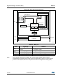
Flexible static memory controller (FSMC) . . . . . . . . . . . . . . . . . . . . . 617
25.1
FSMC main features . . . . . . . . . . . . . . . . . . . . . . . . . . . . . . . . . . . . . . . 617
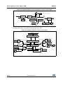
25.2
Block diagram . . . . . . . . . . . . . . . . . . . . . . . . . . . . . . . . . . . . . . . . . . . . . 618
25.3
AHB interface . . . . . . . . . . . . . . . . . . . . . . . . . . . . . . . . . . . . . . . . . . . . . 618
25.3.1
25.4
External device address mapping . . . . . . . . . . . . . . . . . . . . . . . . . . . . . 619
25.4.1
25.5
26
20/901
Supported memories and transactions . . . . . . . . . . . . . . . . . . . . . . . . 619
NOR/PSRAM address mapping . . . . . . . . . . . . . . . . . . . . . . . . . . . . . 620
NOR Flash/PSRAM controller . . . . . . . . . . . . . . . . . . . . . . . . . . . . . . . . 621
25.5.1
External memory interface signals . . . . . . . . . . . . . . . . . . . . . . . . . . . . 622
25.5.2
Supported memories and transactions . . . . . . . . . . . . . . . . . . . . . . . . 623
25.5.3
General timing rules . . . . . . . . . . . . . . . . . . . . . . . . . . . . . . . . . . . . . . . 625
25.5.4
NOR Flash/PSRAM controller asynchronous transactions . . . . . . . . . 625
25.5.5
Synchronous transactions . . . . . . . . . . . . . . . . . . . . . . . . . . . . . . . . . . 643
25.5.6
NOR/PSRAM control registers . . . . . . . . . . . . . . . . . . . . . . . . . . . . . . 649
25.5.7
FSMC register map . . . . . . . . . . . . . . . . . . . . . . . . . . . . . . . . . . . . . . . 656
Inter-integrated circuit (I2C) interface . . . . . . . . . . . . . . . . . . . . . . . . . 657
26.1
I2C introduction . . . . . . . . . . . . . . . . . . . . . . . . . . . . . . . . . . . . . . . . . . . . 657
26.2
I2C main features . . . . . . . . . . . . . . . . . . . . . . . . . . . . . . . . . . . . . . . . . . 657
26.3
I2C functional description . . . . . . . . . . . . . . . . . . . . . . . . . . . . . . . . . . . . 658
26.3.1
Mode selection . . . . . . . . . . . . . . . . . . . . . . . . . . . . . . . . . . . . . . . . . . . 658
26.3.2
I2C slave mode . . . . . . . . . . . . . . . . . . . . . . . . . . . . . . . . . . . . . . . . . . 660
26.3.3
I2C master mode . . . . . . . . . . . . . . . . . . . . . . . . . . . . . . . . . . . . . . . . . 662
26.3.4
Error conditions . . . . . . . . . . . . . . . . . . . . . . . . . . . . . . . . . . . . . . . . . . 668
26.3.5
SDA/SCL line control . . . . . . . . . . . . . . . . . . . . . . . . . . . . . . . . . . . . . . 669
26.3.6
SMBus . . . . . . . . . . . . . . . . . . . . . . . . . . . . . . . . . . . . . . . . . . . . . . . . . 669
26.3.7
DMA requests . . . . . . . . . . . . . . . . . . . . . . . . . . . . . . . . . . . . . . . . . . . 672
26.3.8
Packet error checking . . . . . . . . . . . . . . . . . . . . . . . . . . . . . . . . . . . . . 674
26.4
I2C interrupts . . . . . . . . . . . . . . . . . . . . . . . . . . . . . . . . . . . . . . . . . . . . . 674
26.5
I2C debug mode . . . . . . . . . . . . . . . . . . . . . . . . . . . . . . . . . . . . . . . . . . . 676
26.6
I2C registers . . . . . . . . . . . . . . . . . . . . . . . . . . . . . . . . . . . . . . . . . . . . . . 676
DocID15965 Rev 13
RM0038
Contents
26.6.1
I2C Control register 1 (I2C_CR1) . . . . . . . . . . . . . . . . . . . . . . . . . . . . . 676
26.6.2
I2C Control register 2 (I2C_CR2) . . . . . . . . . . . . . . . . . . . . . . . . . . . . . 678
26.6.3
I2C Own address register 1 (I2C_OAR1) . . . . . . . . . . . . . . . . . . . . . . . 680
26.6.4
I2C Own address register 2 (I2C_OAR2) . . . . . . . . . . . . . . . . . . . . . . . 680
26.6.5
I2C Data register (I2C_DR) . . . . . . . . . . . . . . . . . . . . . . . . . . . . . . . . . 681
26.6.6
I2C Status register 1 (I2C_SR1) . . . . . . . . . . . . . . . . . . . . . . . . . . . . . . 681
26.6.7
I2C Status register 2 (I2C_SR2) . . . . . . . . . . . . . . . . . . . . . . . . . . . . . . 685
26.6.8
I2C Clock control register (I2C_CCR) . . . . . . . . . . . . . . . . . . . . . . . . . 686
26.6.9
I2C TRISE register (I2C_TRISE) . . . . . . . . . . . . . . . . . . . . . . . . . . . . . 687
26.6.10 I2C register map . . . . . . . . . . . . . . . . . . . . . . . . . . . . . . . . . . . . . . . . . 688
27
Universal synchronous asynchronous receiver
transmitter (USART) . . . . . . . . . . . . . . . . . . . . . . . . . . . . . . . . . . . . . . . 689
27.1
USART introduction . . . . . . . . . . . . . . . . . . . . . . . . . . . . . . . . . . . . . . . . 689
27.2
USART main features . . . . . . . . . . . . . . . . . . . . . . . . . . . . . . . . . . . . . . 689
27.3
USART functional description . . . . . . . . . . . . . . . . . . . . . . . . . . . . . . . . 690
27.3.1
USART character description . . . . . . . . . . . . . . . . . . . . . . . . . . . . . . . 693
27.3.2
Transmitter . . . . . . . . . . . . . . . . . . . . . . . . . . . . . . . . . . . . . . . . . . . . . . 694
27.3.3
Receiver . . . . . . . . . . . . . . . . . . . . . . . . . . . . . . . . . . . . . . . . . . . . . . . . 697
27.3.4
Fractional baud rate generation . . . . . . . . . . . . . . . . . . . . . . . . . . . . . . 702
27.3.5
USART receiver tolerance to clock deviation . . . . . . . . . . . . . . . . . . . . 711
27.3.6
Multiprocessor communication . . . . . . . . . . . . . . . . . . . . . . . . . . . . . . 712
27.3.7
Parity control . . . . . . . . . . . . . . . . . . . . . . . . . . . . . . . . . . . . . . . . . . . . 714
27.3.8
LIN (local interconnection network) mode . . . . . . . . . . . . . . . . . . . . . . 715
27.3.9
USART synchronous mode . . . . . . . . . . . . . . . . . . . . . . . . . . . . . . . . . 717
27.3.10 Single-wire half-duplex communication . . . . . . . . . . . . . . . . . . . . . . . . 719
27.3.11 Smartcard . . . . . . . . . . . . . . . . . . . . . . . . . . . . . . . . . . . . . . . . . . . . . . 720
27.3.12 IrDA SIR ENDEC block . . . . . . . . . . . . . . . . . . . . . . . . . . . . . . . . . . . . 722
27.3.13 Continuous communication using DMA . . . . . . . . . . . . . . . . . . . . . . . . 724
27.3.14 Hardware flow control . . . . . . . . . . . . . . . . . . . . . . . . . . . . . . . . . . . . . 726
27.4
USART interrupts . . . . . . . . . . . . . . . . . . . . . . . . . . . . . . . . . . . . . . . . . . 728
27.5
USART mode configuration . . . . . . . . . . . . . . . . . . . . . . . . . . . . . . . . . . 729
27.6
USART registers . . . . . . . . . . . . . . . . . . . . . . . . . . . . . . . . . . . . . . . . . . 729
27.6.1
Status register (USART_SR) . . . . . . . . . . . . . . . . . . . . . . . . . . . . . . . . 729
27.6.2
Data register (USART_DR) . . . . . . . . . . . . . . . . . . . . . . . . . . . . . . . . . 732
27.6.3
Baud rate register (USART_BRR) . . . . . . . . . . . . . . . . . . . . . . . . . . . . 732
27.6.4
Control register 1 (USART_CR1) . . . . . . . . . . . . . . . . . . . . . . . . . . . . . 732
DocID15965 Rev 13
21/901
26
Contents
28
RM0038
27.6.5
Control register 2 (USART_CR2) . . . . . . . . . . . . . . . . . . . . . . . . . . . . . 735
27.6.6
Control register 3 (USART_CR3) . . . . . . . . . . . . . . . . . . . . . . . . . . . . . 736
27.6.7
Guard time and prescaler register (USART_GTPR) . . . . . . . . . . . . . . 738
27.6.8
USART register map . . . . . . . . . . . . . . . . . . . . . . . . . . . . . . . . . . . . . . 739
Serial peripheral interface (SPI) . . . . . . . . . . . . . . . . . . . . . . . . . . . . . . 740
28.1
SPI introduction . . . . . . . . . . . . . . . . . . . . . . . . . . . . . . . . . . . . . . . . . . . 740
28.2
SPI and I2S main features . . . . . . . . . . . . . . . . . . . . . . . . . . . . . . . . . . . 741
28.3
28.2.1
SPI features . . . . . . . . . . . . . . . . . . . . . . . . . . . . . . . . . . . . . . . . . . . . . 741
28.2.2
I2S features . . . . . . . . . . . . . . . . . . . . . . . . . . . . . . . . . . . . . . . . . . . . . 742
SPI functional description . . . . . . . . . . . . . . . . . . . . . . . . . . . . . . . . . . . . 743
28.3.1
General description . . . . . . . . . . . . . . . . . . . . . . . . . . . . . . . . . . . . . . . 743
28.3.2
Configuring the SPI in slave mode . . . . . . . . . . . . . . . . . . . . . . . . . . . 746
28.3.3
Configuring the SPI in master mode . . . . . . . . . . . . . . . . . . . . . . . . . . 749
28.3.4
Configuring the SPI for half-duplex communication . . . . . . . . . . . . . . . 751
28.3.5
Data transmission and reception procedures . . . . . . . . . . . . . . . . . . . 751
28.3.6
CRC calculation . . . . . . . . . . . . . . . . . . . . . . . . . . . . . . . . . . . . . . . . . . 758
28.3.7
Status flags . . . . . . . . . . . . . . . . . . . . . . . . . . . . . . . . . . . . . . . . . . . . . 760
28.3.8
Disabling the SPI . . . . . . . . . . . . . . . . . . . . . . . . . . . . . . . . . . . . . . . . . 761
28.3.9
SPI communication using DMA (direct memory addressing) . . . . . . . 762
28.3.10 Error flags . . . . . . . . . . . . . . . . . . . . . . . . . . . . . . . . . . . . . . . . . . . . . . 764
28.3.11 SPI interrupts . . . . . . . . . . . . . . . . . . . . . . . . . . . . . . . . . . . . . . . . . . . . 765
28.4
28.5
22/901
I2S functional description . . . . . . . . . . . . . . . . . . . . . . . . . . . . . . . . . . . . 766
28.4.1
I2S general description . . . . . . . . . . . . . . . . . . . . . . . . . . . . . . . . . . . . 766
28.4.2
Supported audio protocols . . . . . . . . . . . . . . . . . . . . . . . . . . . . . . . . . . 767
28.4.3
Clock generator . . . . . . . . . . . . . . . . . . . . . . . . . . . . . . . . . . . . . . . . . . 775
28.4.4
I2S master mode . . . . . . . . . . . . . . . . . . . . . . . . . . . . . . . . . . . . . . . . . 777
28.4.5
I2S slave mode . . . . . . . . . . . . . . . . . . . . . . . . . . . . . . . . . . . . . . . . . . 779
28.4.6
Status flags . . . . . . . . . . . . . . . . . . . . . . . . . . . . . . . . . . . . . . . . . . . . . 780
28.4.7
Error flags . . . . . . . . . . . . . . . . . . . . . . . . . . . . . . . . . . . . . . . . . . . . . . 781
28.4.8
I2S interrupts . . . . . . . . . . . . . . . . . . . . . . . . . . . . . . . . . . . . . . . . . . . . 782
SPI and I2S registers . . . . . . . . . . . . . . . . . . . . . . . . . . . . . . . . . . . . . . . 783
28.5.1
SPI control register 1 (SPI_CR1)(not used in I2S mode) . . . . . . . . . . . 783
28.5.2
SPI control register 2 (SPI_CR2) . . . . . . . . . . . . . . . . . . . . . . . . . . . . . 785
28.5.3
SPI status register (SPI_SR) . . . . . . . . . . . . . . . . . . . . . . . . . . . . . . . . 786
28.5.4
SPI data register (SPI_DR) . . . . . . . . . . . . . . . . . . . . . . . . . . . . . . . . . 787
DocID15965 Rev 13
RM0038
Contents
28.5.5
SPI CRC polynomial register (SPI_CRCPR)(not used in I2S
mode) . . . . . . . . . . . . . . . . . . . . . . . . . . . . . . . . . . . . . . . . . . . . . . . . . . 789
28.5.6
SPI RX CRC register (SPI_RXCRCR)(not used in I2S mode) . . . . . . . 789
28.5.7
SPI TX CRC register (SPI_TXCRCR)(not used in I2S mode) . . . . . . . 789
28.5.8
SPI_I2S configuration register (SPI_I2SCFGR) . . . . . . . . . . . . . . . . . . 790
28.5.9
SPI_I2S prescaler register (SPI_I2SPR) . . . . . . . . . . . . . . . . . . . . . . . 791
28.5.10 SPI register map . . . . . . . . . . . . . . . . . . . . . . . . . . . . . . . . . . . . . . . . . 793
29
Secure digital input/output interface (SDIO) . . . . . . . . . . . . . . . . . . . . 794
29.1
SDIO main features . . . . . . . . . . . . . . . . . . . . . . . . . . . . . . . . . . . . . . . . 794
29.2
SDIO bus topology . . . . . . . . . . . . . . . . . . . . . . . . . . . . . . . . . . . . . . . . . 794
29.3
SDIO functional description . . . . . . . . . . . . . . . . . . . . . . . . . . . . . . . . . . 797
29.4
29.3.1
SDIO adapter . . . . . . . . . . . . . . . . . . . . . . . . . . . . . . . . . . . . . . . . . . . . 798
29.3.2
SDIO APB2 interface . . . . . . . . . . . . . . . . . . . . . . . . . . . . . . . . . . . . . . 808
Card functional description . . . . . . . . . . . . . . . . . . . . . . . . . . . . . . . . . . . 809
29.4.1
Card identification mode . . . . . . . . . . . . . . . . . . . . . . . . . . . . . . . . . . . 809
29.4.2
Card reset . . . . . . . . . . . . . . . . . . . . . . . . . . . . . . . . . . . . . . . . . . . . . . 809
29.4.3
Operating voltage range validation . . . . . . . . . . . . . . . . . . . . . . . . . . . 809
29.4.4
Card identification process . . . . . . . . . . . . . . . . . . . . . . . . . . . . . . . . . 810
29.4.5
Block write . . . . . . . . . . . . . . . . . . . . . . . . . . . . . . . . . . . . . . . . . . . . . . 811
29.4.6
Block read . . . . . . . . . . . . . . . . . . . . . . . . . . . . . . . . . . . . . . . . . . . . . . 812
29.4.7
Stream access, stream write and stream read
(MultiMediaCard only) . . . . . . . . . . . . . . . . . . . . . . . . . . . . . . . . . . . . . 812
29.4.8
Erase: group erase and sector erase . . . . . . . . . . . . . . . . . . . . . . . . . 814
29.4.9
Wide bus selection or deselection . . . . . . . . . . . . . . . . . . . . . . . . . . . . 814
29.4.10 Protection management . . . . . . . . . . . . . . . . . . . . . . . . . . . . . . . . . . . . 814
29.4.11 Card status register . . . . . . . . . . . . . . . . . . . . . . . . . . . . . . . . . . . . . . . 817
29.4.12 SD status register . . . . . . . . . . . . . . . . . . . . . . . . . . . . . . . . . . . . . . . . 820
29.4.13 SD I/O mode . . . . . . . . . . . . . . . . . . . . . . . . . . . . . . . . . . . . . . . . . . . . 824
29.4.14 Commands and responses . . . . . . . . . . . . . . . . . . . . . . . . . . . . . . . . . 825
29.5
Response formats . . . . . . . . . . . . . . . . . . . . . . . . . . . . . . . . . . . . . . . . . 829
29.5.1
R1 (normal response command) . . . . . . . . . . . . . . . . . . . . . . . . . . . . . 829
29.5.2
R1b . . . . . . . . . . . . . . . . . . . . . . . . . . . . . . . . . . . . . . . . . . . . . . . . . . . 829
29.5.3
R2 (CID, CSD register) . . . . . . . . . . . . . . . . . . . . . . . . . . . . . . . . . . . . 829
29.5.4
R3 (OCR register) . . . . . . . . . . . . . . . . . . . . . . . . . . . . . . . . . . . . . . . . 830
29.5.5
R4 (Fast I/O) . . . . . . . . . . . . . . . . . . . . . . . . . . . . . . . . . . . . . . . . . . . . 830
29.5.6
R4b . . . . . . . . . . . . . . . . . . . . . . . . . . . . . . . . . . . . . . . . . . . . . . . . . . . 831
DocID15965 Rev 13
23/901
26
Contents
RM0038
29.6
29.7
29.5.7
R5 (interrupt request) . . . . . . . . . . . . . . . . . . . . . . . . . . . . . . . . . . . . . . 831
29.5.8
R6 . . . . . . . . . . . . . . . . . . . . . . . . . . . . . . . . . . . . . . . . . . . . . . . . . . . . 832
SDIO I/O card-specific operations . . . . . . . . . . . . . . . . . . . . . . . . . . . . . 832
29.6.1
SDIO I/O read wait operation by SDIO_D2 signaling . . . . . . . . . . . . . 833
29.6.2
SDIO read wait operation by stopping SDIO_CK . . . . . . . . . . . . . . . . 833
29.6.3
SDIO suspend/resume operation . . . . . . . . . . . . . . . . . . . . . . . . . . . . 833
29.6.4
SDIO interrupts . . . . . . . . . . . . . . . . . . . . . . . . . . . . . . . . . . . . . . . . . . 833
CE-ATA specific operations . . . . . . . . . . . . . . . . . . . . . . . . . . . . . . . . . . 834
29.7.1
Command completion signal disable . . . . . . . . . . . . . . . . . . . . . . . . . . 834
29.7.2
Command completion signal enable . . . . . . . . . . . . . . . . . . . . . . . . . . 834
29.7.3
CE-ATA interrupt . . . . . . . . . . . . . . . . . . . . . . . . . . . . . . . . . . . . . . . . . 834
29.7.4
Aborting CMD61 . . . . . . . . . . . . . . . . . . . . . . . . . . . . . . . . . . . . . . . . . 834
29.8
HW flow control . . . . . . . . . . . . . . . . . . . . . . . . . . . . . . . . . . . . . . . . . . . 835
29.9
SDIO registers . . . . . . . . . . . . . . . . . . . . . . . . . . . . . . . . . . . . . . . . . . . . 835
29.9.1
SDIO power control register (SDIO_POWER) . . . . . . . . . . . . . . . . . . . 835
29.9.2
SDI clock control register (SDIO_CLKCR) . . . . . . . . . . . . . . . . . . . . . 836
29.9.3
SDIO argument register (SDIO_ARG) . . . . . . . . . . . . . . . . . . . . . . . . . 837
29.9.4
SDIO command register (SDIO_CMD) . . . . . . . . . . . . . . . . . . . . . . . . 838
29.9.5
SDIO command response register (SDIO_RESPCMD) . . . . . . . . . . . 839
29.9.6
SDIO response 1..4 register (SDIO_RESPx) . . . . . . . . . . . . . . . . . . . 839
29.9.7
SDIO data timer register (SDIO_DTIMER) . . . . . . . . . . . . . . . . . . . . . 840
29.9.8
SDIO data length register (SDIO_DLEN) . . . . . . . . . . . . . . . . . . . . . . 840
29.9.9
SDIO data control register (SDIO_DCTRL) . . . . . . . . . . . . . . . . . . . . . 841
29.9.10 SDIO data counter register (SDIO_DCOUNT) . . . . . . . . . . . . . . . . . . . 842
29.9.11 SDIO status register (SDIO_STA) . . . . . . . . . . . . . . . . . . . . . . . . . . . . 843
29.9.12 SDIO interrupt clear register (SDIO_ICR) . . . . . . . . . . . . . . . . . . . . . . 844
29.9.13 SDIO mask register (SDIO_MASK) . . . . . . . . . . . . . . . . . . . . . . . . . . . 846
29.9.14 SDIO FIFO counter register (SDIO_FIFOCNT) . . . . . . . . . . . . . . . . . . 848
29.9.15 SDIO data FIFO register (SDIO_FIFO) . . . . . . . . . . . . . . . . . . . . . . . . 849
29.9.16 SDIO register map . . . . . . . . . . . . . . . . . . . . . . . . . . . . . . . . . . . . . . . . 849
30
Debug support (DBG) . . . . . . . . . . . . . . . . . . . . . . . . . . . . . . . . . . . . . . 851
30.1
Overview . . . . . . . . . . . . . . . . . . . . . . . . . . . . . . . . . . . . . . . . . . . . . . . . 851
30.2
Reference ARM® documentation . . . . . . . . . . . . . . . . . . . . . . . . . . . . . . 852
30.3
SWJ debug port (serial wire and JTAG) . . . . . . . . . . . . . . . . . . . . . . . . . 852
30.3.1
24/901
Mechanism to select the JTAG-DP or the SW-DP . . . . . . . . . . . . . . . . 853
DocID15965 Rev 13
RM0038
Contents
30.4
Pinout and debug port pins . . . . . . . . . . . . . . . . . . . . . . . . . . . . . . . . . . 853
30.4.1
SWJ debug port pins . . . . . . . . . . . . . . . . . . . . . . . . . . . . . . . . . . . . . . 854
30.4.2
Flexible SWJ-DP pin assignment . . . . . . . . . . . . . . . . . . . . . . . . . . . . 854
30.4.3
Internal pull-up and pull-down on JTAG pins . . . . . . . . . . . . . . . . . . . . 855
30.4.4
Using serial wire and releasing the unused debug pins as GPIOs . . . 856
30.5
STM32L1xxxx JTAG TAP connection . . . . . . . . . . . . . . . . . . . . . . . . . . 856
30.6
ID codes and locking mechanism . . . . . . . . . . . . . . . . . . . . . . . . . . . . . . 858
30.6.1
MCU device ID code . . . . . . . . . . . . . . . . . . . . . . . . . . . . . . . . . . . . . . 858
30.6.2
Boundary scan TAP . . . . . . . . . . . . . . . . . . . . . . . . . . . . . . . . . . . . . . . 859
30.6.3
Cortex®-M3 TAP . . . . . . . . . . . . . . . . . . . . . . . . . . . . . . . . . . . . . . . . . 859
30.6.4
Cortex®-M3 JEDEC-106 ID code . . . . . . . . . . . . . . . . . . . . . . . . . . . . 859
30.7
JTAG debug port . . . . . . . . . . . . . . . . . . . . . . . . . . . . . . . . . . . . . . . . . . 859
30.8
SW debug port . . . . . . . . . . . . . . . . . . . . . . . . . . . . . . . . . . . . . . . . . . . . 861
30.9
30.8.1
SW protocol introduction . . . . . . . . . . . . . . . . . . . . . . . . . . . . . . . . . . . 861
30.8.2
SW protocol sequence . . . . . . . . . . . . . . . . . . . . . . . . . . . . . . . . . . . . . 861
30.8.3
SW-DP state machine (reset, idle states, ID code) . . . . . . . . . . . . . . . 862
30.8.4
DP and AP read/write accesses . . . . . . . . . . . . . . . . . . . . . . . . . . . . . 862
30.8.5
SW-DP registers . . . . . . . . . . . . . . . . . . . . . . . . . . . . . . . . . . . . . . . . . 863
30.8.6
SW-AP registers . . . . . . . . . . . . . . . . . . . . . . . . . . . . . . . . . . . . . . . . . 864
AHB-AP (AHB access port) - valid for both JTAG-DP
and SW-DP . . . . . . . . . . . . . . . . . . . . . . . . . . . . . . . . . . . . . . . . . . . . . . 864
30.10 Core debug . . . . . . . . . . . . . . . . . . . . . . . . . . . . . . . . . . . . . . . . . . . . . . 865
30.11 Capability of the debugger host to connect under system reset . . . . . . 866
30.12 FPB (Flash patch breakpoint) . . . . . . . . . . . . . . . . . . . . . . . . . . . . . . . . . 866
30.13 DWT (data watchpoint trigger) . . . . . . . . . . . . . . . . . . . . . . . . . . . . . . . . 867
30.14 ITM (instrumentation trace macrocell) . . . . . . . . . . . . . . . . . . . . . . . . . . 867
30.14.1 General description . . . . . . . . . . . . . . . . . . . . . . . . . . . . . . . . . . . . . . . 867
30.14.2 Time stamp packets, synchronization and overflow packets . . . . . . . . 867
30.15 ETM (Embedded trace macrocell) . . . . . . . . . . . . . . . . . . . . . . . . . . . . . 869
30.15.1 General description . . . . . . . . . . . . . . . . . . . . . . . . . . . . . . . . . . . . . . . 869
30.15.2 Signal protocol, packet types . . . . . . . . . . . . . . . . . . . . . . . . . . . . . . . . 869
30.15.3 Main ETM registers . . . . . . . . . . . . . . . . . . . . . . . . . . . . . . . . . . . . . . . 869
30.15.4 Configuration example . . . . . . . . . . . . . . . . . . . . . . . . . . . . . . . . . . . . . 870
30.16 MCU debug component (DBGMCU) . . . . . . . . . . . . . . . . . . . . . . . . . . . 870
30.16.1 Debug support for low-power modes . . . . . . . . . . . . . . . . . . . . . . . . . . 870
30.16.2 Debug support for timers, watchdog and I2C . . . . . . . . . . . . . . . . . . . . 871
DocID15965 Rev 13
25/901
26
Contents
RM0038
30.16.3 Debug MCU configuration register . . . . . . . . . . . . . . . . . . . . . . . . . . . 871
30.16.4 Debug MCU APB1 freeze register (DBGMCU_APB1_FZ) . . . . . . . . . 872
30.16.5 Debug MCU APB2 freeze register (DBGMCU_APB2_FZ) . . . . . . . . . 874
30.17 TPIU (trace port interface unit) . . . . . . . . . . . . . . . . . . . . . . . . . . . . . . . . 875
30.17.1 Introduction . . . . . . . . . . . . . . . . . . . . . . . . . . . . . . . . . . . . . . . . . . . . . 875
30.17.2 TRACE pin assignment . . . . . . . . . . . . . . . . . . . . . . . . . . . . . . . . . . . . 876
30.17.3 TPUI formatter . . . . . . . . . . . . . . . . . . . . . . . . . . . . . . . . . . . . . . . . . . . 877
30.17.4 TPUI frame synchronization packets . . . . . . . . . . . . . . . . . . . . . . . . . . 878
30.17.5 Transmission of the synchronization frame packet . . . . . . . . . . . . . . . 878
30.17.6 Synchronous mode . . . . . . . . . . . . . . . . . . . . . . . . . . . . . . . . . . . . . . . 878
30.17.7 Asynchronous mode . . . . . . . . . . . . . . . . . . . . . . . . . . . . . . . . . . . . . . 879
30.17.8 TRACECLKIN connection inside the STM32L1xxxx . . . . . . . . . . . . . . 879
30.17.9 TPIU registers . . . . . . . . . . . . . . . . . . . . . . . . . . . . . . . . . . . . . . . . . . . 879
30.17.10 Example of configuration . . . . . . . . . . . . . . . . . . . . . . . . . . . . . . . . . . . 880
30.18 DBG register map . . . . . . . . . . . . . . . . . . . . . . . . . . . . . . . . . . . . . . . . . . 880
31
Device electronic signature . . . . . . . . . . . . . . . . . . . . . . . . . . . . . . . . . 882
31.1
Memory size register . . . . . . . . . . . . . . . . . . . . . . . . . . . . . . . . . . . . . . . 882
31.1.1
31.2
32
26/901
Flash size register . . . . . . . . . . . . . . . . . . . . . . . . . . . . . . . . . . . . . . . . 882
Unique device ID registers (96 bits) . . . . . . . . . . . . . . . . . . . . . . . . . . . . 882
Revision history . . . . . . . . . . . . . . . . . . . . . . . . . . . . . . . . . . . . . . . . . . 887
DocID15965 Rev 13
RM0038
List of tables
List of tables
Table 1.
Table 2.
Table 3.
Table 4.
Table 5.
Table 6.
Table 7.
Table 8.
Table 9.
Table 10.
Table 11.
Table 12.
Table 13.
Table 14.
Table 15.
Table 16.
Table 17.
Table 18.
Table 19.
Table 20.
Table 21.
Table 22.
Table 23.
Table 24.
Table 25.
Table 26.
Table 27.
Table 28.
Table 29.
Table 30.
Table 31.
Table 32.
Table 33.
Table 34.
Table 35.
Table 36.
Table 37.
Table 38.
Table 39.
Table 40.
Table 41.
Table 42.
Table 43.
Table 44.
Table 45.
Table 46.
Table 47.
Table 48.
Product categories and memory size overview . . . . . . . . . . . . . . . . . . . . . . . . . . . . . . . . . 40
STM32L100xx product categories . . . . . . . . . . . . . . . . . . . . . . . . . . . . . . . . . . . . . . . . . . . 40
STM32L15xxx product categories . . . . . . . . . . . . . . . . . . . . . . . . . . . . . . . . . . . . . . . . . . . 40
STM32L162xx product categories . . . . . . . . . . . . . . . . . . . . . . . . . . . . . . . . . . . . . . . . . . . 41
Register boundary addresses . . . . . . . . . . . . . . . . . . . . . . . . . . . . . . . . . . . . . . . . . . . . . . . 47
Boot modes. . . . . . . . . . . . . . . . . . . . . . . . . . . . . . . . . . . . . . . . . . . . . . . . . . . . . . . . . . . . . 50
Memory mapping vs. boot mode/physical remap . . . . . . . . . . . . . . . . . . . . . . . . . . . . . . . . 51
NVM module organization (Cat.1 and Cat.2 devices). . . . . . . . . . . . . . . . . . . . . . . . . . . . . 53
NVM module organization (Cat.3 devices) . . . . . . . . . . . . . . . . . . . . . . . . . . . . . . . . . . . . . 54
NVM module organization (Cat.4 devices) . . . . . . . . . . . . . . . . . . . . . . . . . . . . . . . . . . . . . 55
NVM module organization (Cat.5 devices) . . . . . . . . . . . . . . . . . . . . . . . . . . . . . . . . . . . . . 56
NVM module organization (Cat.6 devices) . . . . . . . . . . . . . . . . . . . . . . . . . . . . . . . . . . . . . 58
Number of wait states (WS) according to CPU clock (HCLK) frequency . . . . . . . . . . . . . . 59
Allowed configuration in FLASH_ACR . . . . . . . . . . . . . . . . . . . . . . . . . . . . . . . . . . . . . . . . 61
Data EEPROM programming times . . . . . . . . . . . . . . . . . . . . . . . . . . . . . . . . . . . . . . . . . . 70
Read While Write Summary . . . . . . . . . . . . . . . . . . . . . . . . . . . . . . . . . . . . . . . . . . . . . . . . 71
Prohibited operations . . . . . . . . . . . . . . . . . . . . . . . . . . . . . . . . . . . . . . . . . . . . . . . . . . . . . 72
Option byte organization . . . . . . . . . . . . . . . . . . . . . . . . . . . . . . . . . . . . . . . . . . . . . . . . . . . 73
Description of the option bytes . . . . . . . . . . . . . . . . . . . . . . . . . . . . . . . . . . . . . . . . . . . . . . 75
Programming/erase functions (Cat.1, Cat.2 and Cat.3 devices). . . . . . . . . . . . . . . . . . . . . 77
Programming/erase functions (Cat.4, Cat.5 and Cat.6 devices). . . . . . . . . . . . . . . . . . . . . 79
Flash memory module protection according to RDP and its complement . . . . . . . . . . . . . 81
Interrupts. . . . . . . . . . . . . . . . . . . . . . . . . . . . . . . . . . . . . . . . . . . . . . . . . . . . . . . . . . . . . . . 83
Register map and reset values . . . . . . . . . . . . . . . . . . . . . . . . . . . . . . . . . . . . . . . . . . . . . . 91
CRC calculation unit register map and reset values . . . . . . . . . . . . . . . . . . . . . . . . . . . . . . 96
Performance versus VCORE ranges . . . . . . . . . . . . . . . . . . . . . . . . . . . . . . . . . . . . . . . . 101
Summary of low-power modes . . . . . . . . . . . . . . . . . . . . . . . . . . . . . . . . . . . . . . . . . . . . . 109
Sleep-now . . . . . . . . . . . . . . . . . . . . . . . . . . . . . . . . . . . . . . . . . . . . . . . . . . . . . . . . . . . . . 112
Sleep-on-exit. . . . . . . . . . . . . . . . . . . . . . . . . . . . . . . . . . . . . . . . . . . . . . . . . . . . . . . . . . . 112
Sleep-now . . . . . . . . . . . . . . . . . . . . . . . . . . . . . . . . . . . . . . . . . . . . . . . . . . . . . . . . . . . . . 114
Sleep-on-exit. . . . . . . . . . . . . . . . . . . . . . . . . . . . . . . . . . . . . . . . . . . . . . . . . . . . . . . . . . . 114
Stop mode . . . . . . . . . . . . . . . . . . . . . . . . . . . . . . . . . . . . . . . . . . . . . . . . . . . . . . . . . . . . 116
Standby mode. . . . . . . . . . . . . . . . . . . . . . . . . . . . . . . . . . . . . . . . . . . . . . . . . . . . . . . . . . 117
PWR - register map and reset values . . . . . . . . . . . . . . . . . . . . . . . . . . . . . . . . . . . . . . . . 124
System clock source frequency . . . . . . . . . . . . . . . . . . . . . . . . . . . . . . . . . . . . . . . . . . . . 134
RCC register map and reset values . . . . . . . . . . . . . . . . . . . . . . . . . . . . . . . . . . . . . . . . . 168
Port bit configuration table . . . . . . . . . . . . . . . . . . . . . . . . . . . . . . . . . . . . . . . . . . . . . . . . 173
Flexible SWJ-DP pin assignment . . . . . . . . . . . . . . . . . . . . . . . . . . . . . . . . . . . . . . . . . . . 175
RTC_AF1 pin . . . . . . . . . . . . . . . . . . . . . . . . . . . . . . . . . . . . . . . . . . . . . . . . . . . . . . . . . . 181
GPIO register map and reset values . . . . . . . . . . . . . . . . . . . . . . . . . . . . . . . . . . . . . . . . 189
I/O groups and selection . . . . . . . . . . . . . . . . . . . . . . . . . . . . . . . . . . . . . . . . . . . . . . . . . . 196
Input capture mapping . . . . . . . . . . . . . . . . . . . . . . . . . . . . . . . . . . . . . . . . . . . . . . . . . . . 199
Timer selection . . . . . . . . . . . . . . . . . . . . . . . . . . . . . . . . . . . . . . . . . . . . . . . . . . . . . . . . . 200
Input capture selection . . . . . . . . . . . . . . . . . . . . . . . . . . . . . . . . . . . . . . . . . . . . . . . . . . . 200
RI register map and reset values . . . . . . . . . . . . . . . . . . . . . . . . . . . . . . . . . . . . . . . . . . . 216
SYSCFG register map and reset values. . . . . . . . . . . . . . . . . . . . . . . . . . . . . . . . . . . . . . 222
Acquisition switching sequence summary . . . . . . . . . . . . . . . . . . . . . . . . . . . . . . . . . . . . 226
Channel and sampling capacitor I/Os configuration summary . . . . . . . . . . . . . . . . . . . . . 228
DocID15965 Rev 13
27/901
31
List of tables
Table 49.
Table 50.
Table 51.
Table 52.
Table 53.
Table 54.
Table 55.
Table 56.
Table 57.
Table 58.
Table 59.
Table 60.
Table 61.
Table 62.
Table 63.
Table 64.
Table 65.
Table 66.
Table 67.
Table 68.
Table 69.
Table 70.
Table 71.
Table 72.
Table 73.
Table 74.
Table 75.
Table 76.
Table 77.
Table 78.
Table 79.
Table 80.
Table 81.
Table 82.
Table 83.
Table 84.
Table 85.
Table 86.
Table 87.
Table 88.
Table 89.
Table 90.
Table 91.
Table 92.
Table 93.
Table 94.
Table 95.
Table 96.
Table 97.
Table 98.
Table 99.
Table 100.
28/901
RM0038
Vector table (Cat.1 and Cat.2 devices) . . . . . . . . . . . . . . . . . . . . . . . . . . . . . . . . . . . . . . . 230
Vector table (Cat.3 devices) . . . . . . . . . . . . . . . . . . . . . . . . . . . . . . . . . . . . . . . . . . . . . . . 232
Vector table (Cat.4, Cat.5 and Cat.6 devices) . . . . . . . . . . . . . . . . . . . . . . . . . . . . . . . . . 235
External interrupt/event controller register map and reset values. . . . . . . . . . . . . . . . . . . 244
Programmable data width & endian behavior (when bits PINC = MINC = 1) . . . . . . . . . . 252
DMA interrupt requests . . . . . . . . . . . . . . . . . . . . . . . . . . . . . . . . . . . . . . . . . . . . . . . . . . . 254
Summary of DMA1 requests for each channel . . . . . . . . . . . . . . . . . . . . . . . . . . . . . . . . . 256
Summary of DMA2 requests for each channel . . . . . . . . . . . . . . . . . . . . . . . . . . . . . . . . . 257
DMA register map and reset values . . . . . . . . . . . . . . . . . . . . . . . . . . . . . . . . . . . . . . . . . 263
ADC pins. . . . . . . . . . . . . . . . . . . . . . . . . . . . . . . . . . . . . . . . . . . . . . . . . . . . . . . . . . . . . . 268
Analog watchdog channel selection . . . . . . . . . . . . . . . . . . . . . . . . . . . . . . . . . . . . . . . . . 274
Configuring the trigger edge detection . . . . . . . . . . . . . . . . . . . . . . . . . . . . . . . . . . . . . . . 278
External trigger for regular channels. . . . . . . . . . . . . . . . . . . . . . . . . . . . . . . . . . . . . . . . . 278
External trigger for injected channels . . . . . . . . . . . . . . . . . . . . . . . . . . . . . . . . . . . . . . . . 279
ADC interrupts . . . . . . . . . . . . . . . . . . . . . . . . . . . . . . . . . . . . . . . . . . . . . . . . . . . . . . . . . 290
ADC global register map. . . . . . . . . . . . . . . . . . . . . . . . . . . . . . . . . . . . . . . . . . . . . . . . . . 308
ADC register map and reset values . . . . . . . . . . . . . . . . . . . . . . . . . . . . . . . . . . . . . . . . . 308
ADC register map and reset values (common registers) . . . . . . . . . . . . . . . . . . . . . . . . . 310
DAC pins. . . . . . . . . . . . . . . . . . . . . . . . . . . . . . . . . . . . . . . . . . . . . . . . . . . . . . . . . . . . . . 312
External triggers . . . . . . . . . . . . . . . . . . . . . . . . . . . . . . . . . . . . . . . . . . . . . . . . . . . . . . . . 315
DAC register map . . . . . . . . . . . . . . . . . . . . . . . . . . . . . . . . . . . . . . . . . . . . . . . . . . . . . . . 331
Comparator behavior in the low power modes . . . . . . . . . . . . . . . . . . . . . . . . . . . . . . . . . 339
COMP register map and reset values. . . . . . . . . . . . . . . . . . . . . . . . . . . . . . . . . . . . . . . . 343
Operating modes and calibration . . . . . . . . . . . . . . . . . . . . . . . . . . . . . . . . . . . . . . . . . . . 347
OPAMP register map . . . . . . . . . . . . . . . . . . . . . . . . . . . . . . . . . . . . . . . . . . . . . . . . . . . . 353
Example of frame rate calculation . . . . . . . . . . . . . . . . . . . . . . . . . . . . . . . . . . . . . . . . . . 358
Blink frequency . . . . . . . . . . . . . . . . . . . . . . . . . . . . . . . . . . . . . . . . . . . . . . . . . . . . . . . . . 367
VLCDrail connections to GPIO pins . . . . . . . . . . . . . . . . . . . . . . . . . . . . . . . . . . . . . . . . . . 369
Remapping capability . . . . . . . . . . . . . . . . . . . . . . . . . . . . . . . . . . . . . . . . . . . . . . . . . . . 371
LCD register map and reset values . . . . . . . . . . . . . . . . . . . . . . . . . . . . . . . . . . . . . . . . . 380
Counting direction versus encoder signals . . . . . . . . . . . . . . . . . . . . . . . . . . . . . . . . . . . . 409
TIMx internal trigger connection . . . . . . . . . . . . . . . . . . . . . . . . . . . . . . . . . . . . . . . . . . . . 424
Output control bit for standard OCx channels. . . . . . . . . . . . . . . . . . . . . . . . . . . . . . . . . . 433
TIMx register map and reset values . . . . . . . . . . . . . . . . . . . . . . . . . . . . . . . . . . . . . . . . . 439
TIMx internal trigger connection . . . . . . . . . . . . . . . . . . . . . . . . . . . . . . . . . . . . . . . . . . . . 468
Output control bit for standard OCx channels. . . . . . . . . . . . . . . . . . . . . . . . . . . . . . . . . . 477
TIM9 register map and reset values . . . . . . . . . . . . . . . . . . . . . . . . . . . . . . . . . . . . . . . . . 479
Output control bit for standard OCx channels. . . . . . . . . . . . . . . . . . . . . . . . . . . . . . . . . . 489
TIM10/11 register map and reset values . . . . . . . . . . . . . . . . . . . . . . . . . . . . . . . . . . . . . 493
TIM6&TIM7 register map and reset values. . . . . . . . . . . . . . . . . . . . . . . . . . . . . . . . . . . . 505
Effect of low-power modes on RTC . . . . . . . . . . . . . . . . . . . . . . . . . . . . . . . . . . . . . . . . . 522
Interrupt control bits . . . . . . . . . . . . . . . . . . . . . . . . . . . . . . . . . . . . . . . . . . . . . . . . . . . . . 523
RTC register map and reset values . . . . . . . . . . . . . . . . . . . . . . . . . . . . . . . . . . . . . . . . . 544
Min/max IWDG timeout period at 37 kHz (LSI). . . . . . . . . . . . . . . . . . . . . . . . . . . . . . . . . 548
IWDG register map and reset values . . . . . . . . . . . . . . . . . . . . . . . . . . . . . . . . . . . . . . . . 551
Minimum and maximum timeout values @32 MHz (fPCLK1) . . . . . . . . . . . . . . . . . . . . . . . 555
WWDG register map and reset values . . . . . . . . . . . . . . . . . . . . . . . . . . . . . . . . . . . . . . . 558
Processing time (in clock cycle) . . . . . . . . . . . . . . . . . . . . . . . . . . . . . . . . . . . . . . . . . . . . 575
AES interrupt requests . . . . . . . . . . . . . . . . . . . . . . . . . . . . . . . . . . . . . . . . . . . . . . . . . . . 575
AES register map . . . . . . . . . . . . . . . . . . . . . . . . . . . . . . . . . . . . . . . . . . . . . . . . . . . . . . . 584
Double-buffering buffer flag definition . . . . . . . . . . . . . . . . . . . . . . . . . . . . . . . . . . . . . . . . 595
Bulk double-buffering memory buffers usage . . . . . . . . . . . . . . . . . . . . . . . . . . . . . . . . . . 596
DocID15965 Rev 13
RM0038
Table 101.
Table 102.
Table 103.
Table 104.
Table 105.
Table 106.
Table 107.
Table 108.
Table 109.
Table 110.
Table 111.
Table 112.
Table 113.
Table 114.
Table 115.
Table 116.
Table 117.
Table 118.
Table 119.
Table 120.
Table 121.
Table 122.
Table 123.
Table 124.
Table 125.
Table 126.
Table 127.
Table 128.
Table 129.
Table 130.
Table 131.
Table 132.
Table 133.
Table 134.
Table 135.
Table 136.
Table 137.
Table 138.
Table 139.
Table 140.
Table 141.
Table 142.
Table 143.
Table 144.
Table 145.
Table 146.
List of tables
Isochronous memory buffers usage . . . . . . . . . . . . . . . . . . . . . . . . . . . . . . . . . . . . . . . . . 597
Resume event detection . . . . . . . . . . . . . . . . . . . . . . . . . . . . . . . . . . . . . . . . . . . . . . . . . . 599
Reception status encoding . . . . . . . . . . . . . . . . . . . . . . . . . . . . . . . . . . . . . . . . . . . . . . . . 610
Endpoint type encoding . . . . . . . . . . . . . . . . . . . . . . . . . . . . . . . . . . . . . . . . . . . . . . . . . . 610
Endpoint kind meaning . . . . . . . . . . . . . . . . . . . . . . . . . . . . . . . . . . . . . . . . . . . . . . . . . . . 611
Transmission status encoding . . . . . . . . . . . . . . . . . . . . . . . . . . . . . . . . . . . . . . . . . . . . . 611
Definition of allocated buffer memory . . . . . . . . . . . . . . . . . . . . . . . . . . . . . . . . . . . . . . . . 615
USB register map and reset values . . . . . . . . . . . . . . . . . . . . . . . . . . . . . . . . . . . . . . . . . 615
NOR/PSRAM bank selection . . . . . . . . . . . . . . . . . . . . . . . . . . . . . . . . . . . . . . . . . . . . . . 620
External memory address . . . . . . . . . . . . . . . . . . . . . . . . . . . . . . . . . . . . . . . . . . . . . . . . . 620
Programmable NOR/PSRAM access parameters . . . . . . . . . . . . . . . . . . . . . . . . . . . . . . 621
Nonmultiplexed I/O NOR Flash . . . . . . . . . . . . . . . . . . . . . . . . . . . . . . . . . . . . . . . . . . . . 622
Multiplexed I/O NOR Flash . . . . . . . . . . . . . . . . . . . . . . . . . . . . . . . . . . . . . . . . . . . . . . . . 622
Nonmultiplexed I/Os PSRAM/SRAM . . . . . . . . . . . . . . . . . . . . . . . . . . . . . . . . . . . . . . . . 623
Multiplexed I/O PSRAM . . . . . . . . . . . . . . . . . . . . . . . . . . . . . . . . . . . . . . . . . . . . . . . . . . 623
NOR Flash/PSRAM controller: example of supported memories
and transactions . . . . . . . . . . . . . . . . . . . . . . . . . . . . . . . . . . . . . . . . . . . . . . . . . . . . . . . . 624
FSMC_BCRx bit fields . . . . . . . . . . . . . . . . . . . . . . . . . . . . . . . . . . . . . . . . . . . . . . . . . . . 627
FSMC_BTRx bit fields . . . . . . . . . . . . . . . . . . . . . . . . . . . . . . . . . . . . . . . . . . . . . . . . . . . 627
FSMC_BCRx bit fields . . . . . . . . . . . . . . . . . . . . . . . . . . . . . . . . . . . . . . . . . . . . . . . . . . . 629
FSMC_BTRx bit fields . . . . . . . . . . . . . . . . . . . . . . . . . . . . . . . . . . . . . . . . . . . . . . . . . . . 629
FSMC_BWTRx bit fields . . . . . . . . . . . . . . . . . . . . . . . . . . . . . . . . . . . . . . . . . . . . . . . . . . 630
FSMC_BCRx bit fields . . . . . . . . . . . . . . . . . . . . . . . . . . . . . . . . . . . . . . . . . . . . . . . . . . . 632
FSMC_BTRx bit fields . . . . . . . . . . . . . . . . . . . . . . . . . . . . . . . . . . . . . . . . . . . . . . . . . . . 632
FSMC_BWTRx bit fields . . . . . . . . . . . . . . . . . . . . . . . . . . . . . . . . . . . . . . . . . . . . . . . . . . 633
FSMC_BCRx bit fields . . . . . . . . . . . . . . . . . . . . . . . . . . . . . . . . . . . . . . . . . . . . . . . . . . . 634
FSMC_BTRx bit fields . . . . . . . . . . . . . . . . . . . . . . . . . . . . . . . . . . . . . . . . . . . . . . . . . . . 635
FSMC_BWTRx bit fields . . . . . . . . . . . . . . . . . . . . . . . . . . . . . . . . . . . . . . . . . . . . . . . . . . 635
FSMC_BCRx bit fields . . . . . . . . . . . . . . . . . . . . . . . . . . . . . . . . . . . . . . . . . . . . . . . . . . . 637
FSMC_BTRx bit fields . . . . . . . . . . . . . . . . . . . . . . . . . . . . . . . . . . . . . . . . . . . . . . . . . . . 637
FSMC_BWTRx bit fields . . . . . . . . . . . . . . . . . . . . . . . . . . . . . . . . . . . . . . . . . . . . . . . . . . 638
FSMC_BCRx bit fields . . . . . . . . . . . . . . . . . . . . . . . . . . . . . . . . . . . . . . . . . . . . . . . . . . . 639
FSMC_BTRx bit fields . . . . . . . . . . . . . . . . . . . . . . . . . . . . . . . . . . . . . . . . . . . . . . . . . . . 640
FSMC_BCRx bit fields . . . . . . . . . . . . . . . . . . . . . . . . . . . . . . . . . . . . . . . . . . . . . . . . . . . 645
FSMC_BTRx bit fields . . . . . . . . . . . . . . . . . . . . . . . . . . . . . . . . . . . . . . . . . . . . . . . . . . . 646
FSMC_BCRx bit fields . . . . . . . . . . . . . . . . . . . . . . . . . . . . . . . . . . . . . . . . . . . . . . . . . . . 647
FSMC_BTRx bit fields . . . . . . . . . . . . . . . . . . . . . . . . . . . . . . . . . . . . . . . . . . . . . . . . . . . 648
FSMC register map. . . . . . . . . . . . . . . . . . . . . . . . . . . . . . . . . . . . . . . . . . . . . . . . . . . . . . 656
SMBus vs. I2C . . . . . . . . . . . . . . . . . . . . . . . . . . . . . . . . . . . . . . . . . . . . . . . . . . . . . . . . . 670
I2C Interrupt requests . . . . . . . . . . . . . . . . . . . . . . . . . . . . . . . . . . . . . . . . . . . . . . . . . . . . 674
I2C register map and reset values . . . . . . . . . . . . . . . . . . . . . . . . . . . . . . . . . . . . . . . . . . 688
Noise detection from sampled data . . . . . . . . . . . . . . . . . . . . . . . . . . . . . . . . . . . . . . . . . 701
Error calculation for programmed baud rates at fPCLK = 8 MHz or fPCLK = 12 MHz,
oversampling by 16. . . . . . . . . . . . . . . . . . . . . . . . . . . . . . . . . . . . . . . . . . . . . . . . . . . . . . 704
Error calculation for programmed baud rates at fPCLK = 8 MHz or fPCLK =12 MHz,
oversampling by 8. . . . . . . . . . . . . . . . . . . . . . . . . . . . . . . . . . . . . . . . . . . . . . . . . . . . . . . 705
Error calculation for programmed baud rates at fPCLK = 16 MHz or fPCLK = 24 MHz,
oversampling by 16. . . . . . . . . . . . . . . . . . . . . . . . . . . . . . . . . . . . . . . . . . . . . . . . . . . . . . 705
Error calculation for programmed baud rates at fPCLK = 16 MHz or fPCLK = 24 MHz,
oversampling by 8. . . . . . . . . . . . . . . . . . . . . . . . . . . . . . . . . . . . . . . . . . . . . . . . . . . . . . . 706
Error calculation for programmed baud rates at fPCLK = 1 MHz or fPCLK = 8 MHz),
oversampling by 16. . . . . . . . . . . . . . . . . . . . . . . . . . . . . . . . . . . . . . . . . . . . . . . . . . . . . . 707
DocID15965 Rev 13
29/901
31
List of tables
RM0038
Table 147. Error calculation for programmed baud rates at fPCLK = 1 MHz or fPCLK = 8 MHz),
oversampling by 8. . . . . . . . . . . . . . . . . . . . . . . . . . . . . . . . . . . . . . . . . . . . . . . . . . . . . . . 707
Table 148. Error calculation for programmed baud rates at fPCLK = 16 MHz or fPCLK = 32 MHz),
oversampling by 16. . . . . . . . . . . . . . . . . . . . . . . . . . . . . . . . . . . . . . . . . . . . . . . . . . . . . . 708
Table 149. Error calculation for programmed baud rates at fPCLK = 16 MHz or fPCLK = 32 MHz),
oversampling by 8. . . . . . . . . . . . . . . . . . . . . . . . . . . . . . . . . . . . . . . . . . . . . . . . . . . . . . . 709
Table 150. Error calculation for programmed baud rates at fPCLK = 1 MHz or fPCLK = 8 MHz),
oversampling by 8. . . . . . . . . . . . . . . . . . . . . . . . . . . . . . . . . . . . . . . . . . . . . . . . . . . . . . . 709
Table 151. Error calculation for programmed baud rates at fPCLK = 16 MHz or fPCLK = 32 MHz),
oversampling by 16. . . . . . . . . . . . . . . . . . . . . . . . . . . . . . . . . . . . . . . . . . . . . . . . . . . . . . 710
Table 152. Error calculation for programmed baud rates at fPCLK = 16 MHz or fPCLK = 32 MHz),
oversampling by 8. . . . . . . . . . . . . . . . . . . . . . . . . . . . . . . . . . . . . . . . . . . . . . . . . . . . . . . 711
Table 153. USART receiver’s tolerance when DIV fraction is 0 . . . . . . . . . . . . . . . . . . . . . . . . . . . . . 712
Table 154. USART receiver tolerance when DIV_Fraction is different from 0 . . . . . . . . . . . . . . . . . . 712
Table 155. Frame formats . . . . . . . . . . . . . . . . . . . . . . . . . . . . . . . . . . . . . . . . . . . . . . . . . . . . . . . . . 714
Table 156. USART interrupt requests. . . . . . . . . . . . . . . . . . . . . . . . . . . . . . . . . . . . . . . . . . . . . . . . . 728
Table 157. USART mode configuration . . . . . . . . . . . . . . . . . . . . . . . . . . . . . . . . . . . . . . . . . . . . . . . 729
Table 158. USART register map and reset values . . . . . . . . . . . . . . . . . . . . . . . . . . . . . . . . . . . . . . . 739
Table 159. SPI interrupt requests . . . . . . . . . . . . . . . . . . . . . . . . . . . . . . . . . . . . . . . . . . . . . . . . . . . . 765
Table 160. Audio-frequency precision using standard 8 MHz HSE (Cat.3, Cat.4, Cat.5
and Cat.6 devices only) . . . . . . . . . . . . . . . . . . . . . . . . . . . . . . . . . . . . . . . . . . . . . . . . . . 776
Table 161. I2S interrupt requests . . . . . . . . . . . . . . . . . . . . . . . . . . . . . . . . . . . . . . . . . . . . . . . . . . . . 782
Table 162. SPI register map and reset values . . . . . . . . . . . . . . . . . . . . . . . . . . . . . . . . . . . . . . . . . . 793
Table 163. SDIO I/O definitions . . . . . . . . . . . . . . . . . . . . . . . . . . . . . . . . . . . . . . . . . . . . . . . . . . . . . 798
Table 164. Command format . . . . . . . . . . . . . . . . . . . . . . . . . . . . . . . . . . . . . . . . . . . . . . . . . . . . . . . 802
Table 165. Short response format . . . . . . . . . . . . . . . . . . . . . . . . . . . . . . . . . . . . . . . . . . . . . . . . . . . 803
Table 166. Long response format . . . . . . . . . . . . . . . . . . . . . . . . . . . . . . . . . . . . . . . . . . . . . . . . . . . . 803
Table 167. Command path status flags . . . . . . . . . . . . . . . . . . . . . . . . . . . . . . . . . . . . . . . . . . . . . . . 803
Table 168. Data token format . . . . . . . . . . . . . . . . . . . . . . . . . . . . . . . . . . . . . . . . . . . . . . . . . . . . . . . 806
Table 169. Transmit FIFO status flags . . . . . . . . . . . . . . . . . . . . . . . . . . . . . . . . . . . . . . . . . . . . . . . . 807
Table 170. Receive FIFO status flags . . . . . . . . . . . . . . . . . . . . . . . . . . . . . . . . . . . . . . . . . . . . . . . . 808
Table 171. Card status . . . . . . . . . . . . . . . . . . . . . . . . . . . . . . . . . . . . . . . . . . . . . . . . . . . . . . . . . . . . 818
Table 172. SD status . . . . . . . . . . . . . . . . . . . . . . . . . . . . . . . . . . . . . . . . . . . . . . . . . . . . . . . . . . . . . 821
Table 173. Speed class code field . . . . . . . . . . . . . . . . . . . . . . . . . . . . . . . . . . . . . . . . . . . . . . . . . . . 822
Table 174. Performance move field . . . . . . . . . . . . . . . . . . . . . . . . . . . . . . . . . . . . . . . . . . . . . . . . . . 822
Table 175. AU_SIZE field . . . . . . . . . . . . . . . . . . . . . . . . . . . . . . . . . . . . . . . . . . . . . . . . . . . . . . . . . . 823
Table 176. Maximum AU size . . . . . . . . . . . . . . . . . . . . . . . . . . . . . . . . . . . . . . . . . . . . . . . . . . . . . . . 823
Table 177. Erase size field . . . . . . . . . . . . . . . . . . . . . . . . . . . . . . . . . . . . . . . . . . . . . . . . . . . . . . . . . 823
Table 178. Erase timeout field . . . . . . . . . . . . . . . . . . . . . . . . . . . . . . . . . . . . . . . . . . . . . . . . . . . . . . 824
Table 179. Erase offset field . . . . . . . . . . . . . . . . . . . . . . . . . . . . . . . . . . . . . . . . . . . . . . . . . . . . . . . . 824
Table 180. Block-oriented write commands . . . . . . . . . . . . . . . . . . . . . . . . . . . . . . . . . . . . . . . . . . . . 826
Table 181. Block-oriented write protection commands . . . . . . . . . . . . . . . . . . . . . . . . . . . . . . . . . . . . 827
Table 182. Erase commands . . . . . . . . . . . . . . . . . . . . . . . . . . . . . . . . . . . . . . . . . . . . . . . . . . . . . . . 827
Table 183. I/O mode commands . . . . . . . . . . . . . . . . . . . . . . . . . . . . . . . . . . . . . . . . . . . . . . . . . . . . 828
Table 184. Lock card . . . . . . . . . . . . . . . . . . . . . . . . . . . . . . . . . . . . . . . . . . . . . . . . . . . . . . . . . . . . . 828
Table 185. Application-specific commands . . . . . . . . . . . . . . . . . . . . . . . . . . . . . . . . . . . . . . . . . . . . 828
Table 186. R1 response . . . . . . . . . . . . . . . . . . . . . . . . . . . . . . . . . . . . . . . . . . . . . . . . . . . . . . . . . . . 829
Table 187. R2 response . . . . . . . . . . . . . . . . . . . . . . . . . . . . . . . . . . . . . . . . . . . . . . . . . . . . . . . . . . . 830
Table 188. R3 response . . . . . . . . . . . . . . . . . . . . . . . . . . . . . . . . . . . . . . . . . . . . . . . . . . . . . . . . . . . 830
Table 189. R4 response . . . . . . . . . . . . . . . . . . . . . . . . . . . . . . . . . . . . . . . . . . . . . . . . . . . . . . . . . . . 830
Table 190. R4b response . . . . . . . . . . . . . . . . . . . . . . . . . . . . . . . . . . . . . . . . . . . . . . . . . . . . . . . . . . 831
Table 191. R5 response . . . . . . . . . . . . . . . . . . . . . . . . . . . . . . . . . . . . . . . . . . . . . . . . . . . . . . . . . . . 831
30/901
DocID15965 Rev 13
RM0038
Table 192.
Table 193.
Table 194.
Table 195.
Table 196.
Table 197.
Table 198.
Table 199.
Table 200.
Table 201.
Table 202.
Table 203.
Table 204.
Table 205.
Table 206.
Table 207.
Table 208.
Table 209.
Table 210.
Table 211.
Table 212.
List of tables
R6 response . . . . . . . . . . . . . . . . . . . . . . . . . . . . . . . . . . . . . . . . . . . . . . . . . . . . . . . . . . . 832
Response type and SDIO_RESPx registers. . . . . . . . . . . . . . . . . . . . . . . . . . . . . . . . . . . 839
SDIO register map . . . . . . . . . . . . . . . . . . . . . . . . . . . . . . . . . . . . . . . . . . . . . . . . . . . . . . 849
SWJ debug port pins . . . . . . . . . . . . . . . . . . . . . . . . . . . . . . . . . . . . . . . . . . . . . . . . . . . . 854
Flexible SWJ-DP pin assignment . . . . . . . . . . . . . . . . . . . . . . . . . . . . . . . . . . . . . . . . . . . 854
JTAG debug port data registers . . . . . . . . . . . . . . . . . . . . . . . . . . . . . . . . . . . . . . . . . . . . 859
32-bit debug port registers addressed through the shifted value A[3:2] . . . . . . . . . . . . . . 860
Packet request (8-bits) . . . . . . . . . . . . . . . . . . . . . . . . . . . . . . . . . . . . . . . . . . . . . . . . . . . 861
ACK response (3 bits). . . . . . . . . . . . . . . . . . . . . . . . . . . . . . . . . . . . . . . . . . . . . . . . . . . . 862
DATA transfer (33 bits) . . . . . . . . . . . . . . . . . . . . . . . . . . . . . . . . . . . . . . . . . . . . . . . . . . . 862
SW-DP registers . . . . . . . . . . . . . . . . . . . . . . . . . . . . . . . . . . . . . . . . . . . . . . . . . . . . . . . . 863
Cortex®-M3 AHB-AP registers . . . . . . . . . . . . . . . . . . . . . . . . . . . . . . . . . . . . . . . . . . . . . 864
Core debug registers . . . . . . . . . . . . . . . . . . . . . . . . . . . . . . . . . . . . . . . . . . . . . . . . . . . . 865
Main ITM registers . . . . . . . . . . . . . . . . . . . . . . . . . . . . . . . . . . . . . . . . . . . . . . . . . . . . . . 868
Main ETM registers. . . . . . . . . . . . . . . . . . . . . . . . . . . . . . . . . . . . . . . . . . . . . . . . . . . . . . 870
Asynchronous TRACE pin assignment. . . . . . . . . . . . . . . . . . . . . . . . . . . . . . . . . . . . . . . 876
Synchronous TRACE pin assignment . . . . . . . . . . . . . . . . . . . . . . . . . . . . . . . . . . . . . . . 876
Flexible TRACE pin assignment . . . . . . . . . . . . . . . . . . . . . . . . . . . . . . . . . . . . . . . . . . . . 877
Important TPIU registers. . . . . . . . . . . . . . . . . . . . . . . . . . . . . . . . . . . . . . . . . . . . . . . . . . 879
DBG register map and reset values . . . . . . . . . . . . . . . . . . . . . . . . . . . . . . . . . . . . . . . . . 881
Document revision history . . . . . . . . . . . . . . . . . . . . . . . . . . . . . . . . . . . . . . . . . . . . . . . . 887
DocID15965 Rev 13
31/901
31
List of figures
RM0038
List of figures
Figure 1.
Figure 2.
Figure 3.
Figure 4.
Figure 5.
Figure 6.
Figure 7.
Figure 8.
Figure 9.
Figure 10.
Figure 11.
Figure 12.
Figure 13.
Figure 14.
Figure 15.
Figure 16.
Figure 17.
Figure 18.
Figure 19.
Figure 20.
Figure 21.
Figure 22.
Figure 23.
Figure 24.
Figure 25.
Figure 26.
Figure 27.
Figure 28.
Figure 29.
Figure 30.
Figure 31.
Figure 32.
Figure 33.
Figure 34.
Figure 35.
Figure 36.
Figure 37.
Figure 38.
Figure 39.
Figure 40.
Figure 41.
Figure 42.
Figure 43.
Figure 44.
Figure 45.
Figure 46.
Figure 47.
32/901
System architecture (Cat.1 and Cat.2 devices) . . . . . . . . . . . . . . . . . . . . . . . . . . . . . . . . . 42
System architecture (Cat.3 devices) . . . . . . . . . . . . . . . . . . . . . . . . . . . . . . . . . . . . . . . . . . 43
System architecture (Cat.4 devices) . . . . . . . . . . . . . . . . . . . . . . . . . . . . . . . . . . . . . . . . . . 44
System architecture (Cat.5 and Cat.6 devices) . . . . . . . . . . . . . . . . . . . . . . . . . . . . . . . . . 45
Sequential 32 bits instructions execution . . . . . . . . . . . . . . . . . . . . . . . . . . . . . . . . . . . . . . 61
RDP levels . . . . . . . . . . . . . . . . . . . . . . . . . . . . . . . . . . . . . . . . . . . . . . . . . . . . . . . . . . . . . 81
CRC calculation unit block diagram . . . . . . . . . . . . . . . . . . . . . . . . . . . . . . . . . . . . . . . . . . 94
Power supply overview . . . . . . . . . . . . . . . . . . . . . . . . . . . . . . . . . . . . . . . . . . . . . . . . . . . . 98
STM32L1xxxx performance versus VDD and VCORE range. . . . . . . . . . . . . . . . . . . . . . 102
Power supply supervisors . . . . . . . . . . . . . . . . . . . . . . . . . . . . . . . . . . . . . . . . . . . . . . . . 105
Power on reset/power down reset waveform . . . . . . . . . . . . . . . . . . . . . . . . . . . . . . . . . . 106
BOR thresholds . . . . . . . . . . . . . . . . . . . . . . . . . . . . . . . . . . . . . . . . . . . . . . . . . . . . . . . . 107
PVD thresholds . . . . . . . . . . . . . . . . . . . . . . . . . . . . . . . . . . . . . . . . . . . . . . . . . . . . . . . . . 108
Simplified diagram of the reset circuit . . . . . . . . . . . . . . . . . . . . . . . . . . . . . . . . . . . . . . . . 127
Clock tree . . . . . . . . . . . . . . . . . . . . . . . . . . . . . . . . . . . . . . . . . . . . . . . . . . . . . . . . . . . . . 129
HSE/ LSE clock sources . . . . . . . . . . . . . . . . . . . . . . . . . . . . . . . . . . . . . . . . . . . . . . . . . . 130
Using the TIM9/TIM10/TIM11 channel 1 input capture to measure
frequencies . . . . . . . . . . . . . . . . . . . . . . . . . . . . . . . . . . . . . . . . . . . . . . . . . . . . . . . . . . . . 137
Basic structure of a standard I/O port bit . . . . . . . . . . . . . . . . . . . . . . . . . . . . . . . . . . . . . 172
Basic structure of a five-volt tolerant I/O port bit . . . . . . . . . . . . . . . . . . . . . . . . . . . . . . . . 173
Selecting an alternate function . . . . . . . . . . . . . . . . . . . . . . . . . . . . . . . . . . . . . . . . . . . 176
Input floating/pull up/pull down configurations . . . . . . . . . . . . . . . . . . . . . . . . . . . . . . . . . 178
Output configuration . . . . . . . . . . . . . . . . . . . . . . . . . . . . . . . . . . . . . . . . . . . . . . . . . . . . . 179
Alternate function configuration . . . . . . . . . . . . . . . . . . . . . . . . . . . . . . . . . . . . . . . . . . . . 180
High impedance-analog configuration . . . . . . . . . . . . . . . . . . . . . . . . . . . . . . . . . . . . . . . 180
Routing interface (RI) block diagram for Cat.1 and Cat.2 devices . . . . . . . . . . . . . . . . . . 192
Routing interface (RI) block diagram for Cat.3 devices . . . . . . . . . . . . . . . . . . . . . . . . . . 193
Routing interface (RI) block diagram for Cat.4, Cat.5 and Cat.6 devices . . . . . . . . . . . . . 194
Internal reference voltage output . . . . . . . . . . . . . . . . . . . . . . . . . . . . . . . . . . . . . . . . . . . 200
Surface charge transfer analog IO group structure . . . . . . . . . . . . . . . . . . . . . . . . . . . . . 225
Sampling capacitor charge overview . . . . . . . . . . . . . . . . . . . . . . . . . . . . . . . . . . . . . . . . 227
Timer mode acquisition logic . . . . . . . . . . . . . . . . . . . . . . . . . . . . . . . . . . . . . . . . . . . . . . 228
External interrupt/event controller block diagram . . . . . . . . . . . . . . . . . . . . . . . . . . . . . . . 238
External interrupt/event GPIO mapping . . . . . . . . . . . . . . . . . . . . . . . . . . . . . . . . . . . . . . 240
DMA block diagram in Cat.1 and Cat.2 STM32L1xxxx devices . . . . . . . . . . . . . . . . . . . . 247
DMA block diagram in Cat.3 STM32L1xxxx devices . . . . . . . . . . . . . . . . . . . . . . . . . . . . 248
DMA block diagram in Cat.4, Cat.5 and Cat.6 STM32L1xxxx devices . . . . . . . . . . . . . . 249
DMA1 request mapping . . . . . . . . . . . . . . . . . . . . . . . . . . . . . . . . . . . . . . . . . . . . . . . . . . 255
DMA2 request mapping . . . . . . . . . . . . . . . . . . . . . . . . . . . . . . . . . . . . . . . . . . . . . . . . . 257
ADC block diagram (Cat.1 and Cat.2 devices) . . . . . . . . . . . . . . . . . . . . . . . . . . . . . . . . . 267
ADC block diagram (Cat.3, Cat.4, Cat.5 and Cat.6 devices) . . . . . . . . . . . . . . . . . . . . . . 269
Timing diagram (normal mode, PDI=0). . . . . . . . . . . . . . . . . . . . . . . . . . . . . . . . . . . . . . . 273
Analog watchdog’s guarded area . . . . . . . . . . . . . . . . . . . . . . . . . . . . . . . . . . . . . . . . . . . 273
Injected conversion latency . . . . . . . . . . . . . . . . . . . . . . . . . . . . . . . . . . . . . . . . . . . . . . . 275
Right alignment of 12-bit data . . . . . . . . . . . . . . . . . . . . . . . . . . . . . . . . . . . . . . . . . . . . . . 277
Left alignment of 12-bit data . . . . . . . . . . . . . . . . . . . . . . . . . . . . . . . . . . . . . . . . . . . . . . . 277
Left alignment of 6-bit data . . . . . . . . . . . . . . . . . . . . . . . . . . . . . . . . . . . . . . . . . . . . . . . . 277
ADC freeze mode . . . . . . . . . . . . . . . . . . . . . . . . . . . . . . . . . . . . . . . . . . . . . . . . . . . . . . . 281
DocID15965 Rev 13
RM0038
Figure 48.
Figure 49.
Figure 50.
Figure 51.
Figure 52.
Figure 53.
Figure 54.
Figure 55.
Figure 56.
Figure 57.
Figure 58.
Figure 59.
Figure 60.
Figure 61.
Figure 62.
Figure 63.
Figure 64.
Figure 65.
Figure 66.
Figure 67.
Figure 68.
Figure 69.
Figure 70.
Figure 71.
Figure 72.
Figure 73.
Figure 74.
Figure 75.
Figure 76.
Figure 77.
Figure 78.
Figure 79.
Figure 80.
Figure 81.
Figure 82.
Figure 83.
Figure 84.
Figure 85.
Figure 86.
Figure 87.
Figure 88.
Figure 89.
Figure 90.
Figure 91.
Figure 92.
Figure 93.
Figure 94.
Figure 95.
Figure 96.
Figure 97.
Figure 98.
Figure 99.
List of figures
Continuous regular conversions with a delay . . . . . . . . . . . . . . . . . . . . . . . . . . . . . . . . . . 282
Continuous conversions with a delay between each conversion . . . . . . . . . . . . . . . . . . . 283
Automatic power-down control: example 1 . . . . . . . . . . . . . . . . . . . . . . . . . . . . . . . . . . . . 284
Automatic power-down control: example 2 . . . . . . . . . . . . . . . . . . . . . . . . . . . . . . . . . . . . 284
Automatic power-down control: example 3 . . . . . . . . . . . . . . . . . . . . . . . . . . . . . . . . . . . . 285
Temperature sensor and VREFINT channel block diagram . . . . . . . . . . . . . . . . . . . . . . 287
ADC flags and interrupts. . . . . . . . . . . . . . . . . . . . . . . . . . . . . . . . . . . . . . . . . . . . . . . . . . 289
DAC channel block diagram . . . . . . . . . . . . . . . . . . . . . . . . . . . . . . . . . . . . . . . . . . . . . . 312
Data registers in single DAC channel mode . . . . . . . . . . . . . . . . . . . . . . . . . . . . . . . . . . . 314
Data registers in dual DAC channel mode . . . . . . . . . . . . . . . . . . . . . . . . . . . . . . . . . . . . 314
Timing diagram for conversion with trigger disabled TEN = 0 . . . . . . . . . . . . . . . . . . . . . 315
DAC LFSR register calculation algorithm . . . . . . . . . . . . . . . . . . . . . . . . . . . . . . . . . . . . . 317
DAC conversion (SW trigger enabled) with LFSR wave generation. . . . . . . . . . . . . . . . . 317
DAC triangle wave generation . . . . . . . . . . . . . . . . . . . . . . . . . . . . . . . . . . . . . . . . . . . . . 318
DAC conversion (SW trigger enabled) with triangle wave generation . . . . . . . . . . . . . . . 318
COMP1 interconnections (Cat.1 and Cat.2 devices) . . . . . . . . . . . . . . . . . . . . . . . . . . . . 334
COMP1 interconnections (Cat.3, Cat.4, Cat.5 and Cat.6 devices) . . . . . . . . . . . . . . . . . . 335
COMP2 interconnections (Cat.1 and Cat.2 devices) . . . . . . . . . . . . . . . . . . . . . . . . . . . . 337
COMP2 interconnections (Cat.3, Cat.4, Cat.5 and Cat.6 devices) . . . . . . . . . . . . . . . . . . 337
Redirecting the COMP2 output . . . . . . . . . . . . . . . . . . . . . . . . . . . . . . . . . . . . . . . . . . . . . 338
Comparators in Window mode . . . . . . . . . . . . . . . . . . . . . . . . . . . . . . . . . . . . . . . . . . . . . 339
OPAMP1 signal routing . . . . . . . . . . . . . . . . . . . . . . . . . . . . . . . . . . . . . . . . . . . . . . . . . . 345
OPAMP2 signal routing . . . . . . . . . . . . . . . . . . . . . . . . . . . . . . . . . . . . . . . . . . . . . . . . . . 345
OPAMP3 signal routing (Cat.4 devices only) . . . . . . . . . . . . . . . . . . . . . . . . . . . . . . . . . . 346
LCD controller block diagram . . . . . . . . . . . . . . . . . . . . . . . . . . . . . . . . . . . . . . . . . . . . . 357
1/3 bias, 1/4 duty . . . . . . . . . . . . . . . . . . . . . . . . . . . . . . . . . . . . . . . . . . . . . . . . . . . . . . . 360
Static duty . . . . . . . . . . . . . . . . . . . . . . . . . . . . . . . . . . . . . . . . . . . . . . . . . . . . . . . . . . . . . 361
Static duty . . . . . . . . . . . . . . . . . . . . . . . . . . . . . . . . . . . . . . . . . . . . . . . . . . . . . . . . . . . . . 361
1/2 duty, 1/2 bias . . . . . . . . . . . . . . . . . . . . . . . . . . . . . . . . . . . . . . . . . . . . . . . . . . . . . . . 362
1/3 duty, 1/3 bias . . . . . . . . . . . . . . . . . . . . . . . . . . . . . . . . . . . . . . . . . . . . . . . . . . . . . . . 364
1/4 duty, 1/3 bias . . . . . . . . . . . . . . . . . . . . . . . . . . . . . . . . . . . . . . . . . . . . . . . . . . . . . . . 365
1/8 duty, 1/4 bias . . . . . . . . . . . . . . . . . . . . . . . . . . . . . . . . . . . . . . . . . . . . . . . . . . . . . . . 366
LCD voltage control . . . . . . . . . . . . . . . . . . . . . . . . . . . . . . . . . . . . . . . . . . . . . . . . . . . . . 368
Deadtime . . . . . . . . . . . . . . . . . . . . . . . . . . . . . . . . . . . . . . . . . . . . . . . . . . . . . . . . . . . . . 369
SEG/COM mux feature example . . . . . . . . . . . . . . . . . . . . . . . . . . . . . . . . . . . . . . . . . . . 373
Flowchart example . . . . . . . . . . . . . . . . . . . . . . . . . . . . . . . . . . . . . . . . . . . . . . . . . . . . . . 374
General-purpose timer block diagram . . . . . . . . . . . . . . . . . . . . . . . . . . . . . . . . . . . . . . . 384
Counter timing diagram with prescaler division change from 1 to 2 . . . . . . . . . . . . . . . . . 385
Counter timing diagram with prescaler division change from 1 to 4 . . . . . . . . . . . . . . . . . 386
Counter timing diagram, internal clock divided by 1 . . . . . . . . . . . . . . . . . . . . . . . . . . . . . 387
Counter timing diagram, internal clock divided by 2 . . . . . . . . . . . . . . . . . . . . . . . . . . . . . 387
Counter timing diagram, internal clock divided by 4 . . . . . . . . . . . . . . . . . . . . . . . . . . . . . 387
Counter timing diagram, internal clock divided by N. . . . . . . . . . . . . . . . . . . . . . . . . . . . . 388
Counter timing diagram, Update event when ARPE=0 (TIMx_ARR not preloaded). . . . . 388
Counter timing diagram, Update event when ARPE=1 (TIMx_ARR preloaded). . . . . . . . 389
Counter timing diagram, internal clock divided by 1 . . . . . . . . . . . . . . . . . . . . . . . . . . . . . 390
Counter timing diagram, internal clock divided by 2 . . . . . . . . . . . . . . . . . . . . . . . . . . . . . 390
Counter timing diagram, internal clock divided by 4 . . . . . . . . . . . . . . . . . . . . . . . . . . . . . 390
Counter timing diagram, internal clock divided by N. . . . . . . . . . . . . . . . . . . . . . . . . . . . . 391
Counter timing diagram, Update event . . . . . . . . . . . . . . . . . . . . . . . . . . . . . . . . . . . . . . . 391
Counter timing diagram, internal clock divided by 1, TIMx_ARR=0x6 . . . . . . . . . . . . . . . 392
Counter timing diagram, internal clock divided by 2 . . . . . . . . . . . . . . . . . . . . . . . . . . . . . 393
DocID15965 Rev 13
33/901
37
List of figures
Figure 100.
Figure 101.
Figure 102.
Figure 103.
Figure 104.
Figure 105.
Figure 106.
Figure 107.
Figure 108.
Figure 109.
Figure 110.
Figure 111.
Figure 112.
Figure 113.
Figure 114.
Figure 115.
Figure 116.
Figure 117.
Figure 118.
Figure 119.
Figure 120.
Figure 121.
Figure 122.
Figure 123.
Figure 124.
Figure 125.
Figure 126.
Figure 127.
Figure 128.
Figure 129.
Figure 130.
Figure 131.
Figure 132.
Figure 133.
Figure 134.
Figure 135.
Figure 136.
Figure 137.
Figure 138.
Figure 139.
Figure 140.
Figure 141.
Figure 142.
Figure 143.
Figure 144.
Figure 145.
Figure 146.
Figure 147.
Figure 148.
Figure 149.
34/901
RM0038
Counter timing diagram, internal clock divided by 4, TIMx_ARR=0x36 . . . . . . . . . . . . . . 393
Counter timing diagram, internal clock divided by N. . . . . . . . . . . . . . . . . . . . . . . . . . . . . 393
Counter timing diagram, Update event with ARPE=1 (counter underflow). . . . . . . . . . . . 394
Counter timing diagram, Update event with ARPE=1 (counter overflow) . . . . . . . . . . . . . 394
Control circuit in normal mode, internal clock divided by 1 . . . . . . . . . . . . . . . . . . . . . . . . 395
TI2 external clock connection example. . . . . . . . . . . . . . . . . . . . . . . . . . . . . . . . . . . . . . . 395
Control circuit in external clock mode 1 . . . . . . . . . . . . . . . . . . . . . . . . . . . . . . . . . . . . . . 396
External trigger input block . . . . . . . . . . . . . . . . . . . . . . . . . . . . . . . . . . . . . . . . . . . . . . . . 396
Control circuit in external clock mode 2 . . . . . . . . . . . . . . . . . . . . . . . . . . . . . . . . . . . . . . 397
Capture/compare channel (example: channel 1 input stage) . . . . . . . . . . . . . . . . . . . . . . 398
Capture/compare channel 1 main circuit . . . . . . . . . . . . . . . . . . . . . . . . . . . . . . . . . . . . . 398
Output stage of capture/compare channel (channel 1). . . . . . . . . . . . . . . . . . . . . . . . . . . 399
PWM input mode timing . . . . . . . . . . . . . . . . . . . . . . . . . . . . . . . . . . . . . . . . . . . . . . . . . . 401
Output compare mode, toggle on OC1 . . . . . . . . . . . . . . . . . . . . . . . . . . . . . . . . . . . . . . . 403
Edge-aligned PWM waveforms (ARR=8) . . . . . . . . . . . . . . . . . . . . . . . . . . . . . . . . . . . . . 404
Center-aligned PWM waveforms (ARR=8) . . . . . . . . . . . . . . . . . . . . . . . . . . . . . . . . . . . . 405
Example of one-pulse mode . . . . . . . . . . . . . . . . . . . . . . . . . . . . . . . . . . . . . . . . . . . . . . . 406
Clearing TIMx OCxREF . . . . . . . . . . . . . . . . . . . . . . . . . . . . . . . . . . . . . . . . . . . . . . . . . . 408
Example of counter operation in encoder interface mode . . . . . . . . . . . . . . . . . . . . . . . . 409
Example of encoder interface mode with TI1FP1 polarity inverted . . . . . . . . . . . . . . . . . 410
Control circuit in reset mode . . . . . . . . . . . . . . . . . . . . . . . . . . . . . . . . . . . . . . . . . . . . . . . 411
Control circuit in gated mode . . . . . . . . . . . . . . . . . . . . . . . . . . . . . . . . . . . . . . . . . . . . . . 412
Control circuit in trigger mode . . . . . . . . . . . . . . . . . . . . . . . . . . . . . . . . . . . . . . . . . . . . . . 412
Control circuit in external clock mode 2 + trigger mode . . . . . . . . . . . . . . . . . . . . . . . . . . 413
Master/Slave timer example . . . . . . . . . . . . . . . . . . . . . . . . . . . . . . . . . . . . . . . . . . . . . . 414
Gating TIM2 with OC1REF of TIM3 . . . . . . . . . . . . . . . . . . . . . . . . . . . . . . . . . . . . . . . . . 415
Gating TIM2 with Enable of TIM3 . . . . . . . . . . . . . . . . . . . . . . . . . . . . . . . . . . . . . . . . . . . 416
Triggering TIM2 with update of TIM3 . . . . . . . . . . . . . . . . . . . . . . . . . . . . . . . . . . . . . . . . 416
Triggering TIM2 with Enable of TIM3 . . . . . . . . . . . . . . . . . . . . . . . . . . . . . . . . . . . . . . . . 417
Triggering TIM3 and TIM2 with TIM3 TI1 input. . . . . . . . . . . . . . . . . . . . . . . . . . . . . . . . . 418
General-purpose timer block diagram (TIM9) . . . . . . . . . . . . . . . . . . . . . . . . . . . . . . . . . 443
General-purpose timer block diagram (TIM10) . . . . . . . . . . . . . . . . . . . . . . . . . . . . . . . 444
General-purpose timer block diagram (TIM11) . . . . . . . . . . . . . . . . . . . . . . . . . . . . . . . . . 445
Counter timing diagram with prescaler division change from 1 to 2 . . . . . . . . . . . . . . . . . 447
Counter timing diagram with prescaler division change from 1 to 4 . . . . . . . . . . . . . . . . . 447
Counter timing diagram, internal clock divided by 1 . . . . . . . . . . . . . . . . . . . . . . . . . . . . . 448
Counter timing diagram, internal clock divided by 2 . . . . . . . . . . . . . . . . . . . . . . . . . . . . . 448
Counter timing diagram, internal clock divided by 4 . . . . . . . . . . . . . . . . . . . . . . . . . . . . . 449
Counter timing diagram, internal clock divided by N. . . . . . . . . . . . . . . . . . . . . . . . . . . . . 449
Counter timing diagram, update event when ARPE=0 (TIMx_ARR not
preloaded). . . . . . . . . . . . . . . . . . . . . . . . . . . . . . . . . . . . . . . . . . . . . . . . . . . . . . . . . . . . . 449
Counter timing diagram, update event when ARPE=1 (TIMx_ARR
preloaded). . . . . . . . . . . . . . . . . . . . . . . . . . . . . . . . . . . . . . . . . . . . . . . . . . . . . . . . . . . . . 450
Control circuit in normal mode, internal clock divided by 1 . . . . . . . . . . . . . . . . . . . . . . . . 451
TI2 external clock connection example. . . . . . . . . . . . . . . . . . . . . . . . . . . . . . . . . . . . . . . 451
Control circuit in external clock mode 1 . . . . . . . . . . . . . . . . . . . . . . . . . . . . . . . . . . . . . . 452
Capture/compare channel (example: channel 1 input stage) . . . . . . . . . . . . . . . . . . . . . . 452
Capture/compare channel 1 main circuit . . . . . . . . . . . . . . . . . . . . . . . . . . . . . . . . . . . . . 453
Output stage of capture/compare channel (channel 1). . . . . . . . . . . . . . . . . . . . . . . . . . . 453
PWM input mode timing . . . . . . . . . . . . . . . . . . . . . . . . . . . . . . . . . . . . . . . . . . . . . . . . . . 455
Output compare mode, toggle on OC1. . . . . . . . . . . . . . . . . . . . . . . . . . . . . . . . . . . . . . . 457
Edge-aligned PWM waveforms (ARR=8) . . . . . . . . . . . . . . . . . . . . . . . . . . . . . . . . . . . . . 458
DocID15965 Rev 13
RM0038
Figure 150.
Figure 151.
Figure 152.
Figure 153.
Figure 154.
Figure 155.
Figure 156.
Figure 157.
Figure 158.
Figure 159.
Figure 160.
Figure 161.
Figure 162.
Figure 163.
Figure 164.
Figure 165.
Figure 166.
Figure 167.
Figure 168.
Figure 169.
Figure 170.
Figure 171.
Figure 172.
Figure 173.
Figure 174.
Figure 175.
Figure 176.
Figure 177.
Figure 178.
Figure 179.
Figure 180.
Figure 181.
Figure 182.
Figure 183.
Figure 184.
Figure 185.
Figure 186.
Figure 187.
Figure 188.
Figure 189.
Figure 190.
Figure 191.
Figure 192.
Figure 193.
Figure 194.
Figure 195.
Figure 196.
Figure 197.
Figure 198.
Figure 199.
List of figures
Example of one pulse mode. . . . . . . . . . . . . . . . . . . . . . . . . . . . . . . . . . . . . . . . . . . . . . . 459
Control circuit in reset mode . . . . . . . . . . . . . . . . . . . . . . . . . . . . . . . . . . . . . . . . . . . . . . . 460
Control circuit in gated mode . . . . . . . . . . . . . . . . . . . . . . . . . . . . . . . . . . . . . . . . . . . . . . 461
Control circuit in trigger mode . . . . . . . . . . . . . . . . . . . . . . . . . . . . . . . . . . . . . . . . . . . . . . 462
Basic timer block diagram. . . . . . . . . . . . . . . . . . . . . . . . . . . . . . . . . . . . . . . . . . . . . . . . . 495
Counter timing diagram with prescaler division change from 1 to 2 . . . . . . . . . . . . . . . . . 497
Counter timing diagram with prescaler division change from 1 to 4 . . . . . . . . . . . . . . . . . 497
Counter timing diagram, internal clock divided by 1 . . . . . . . . . . . . . . . . . . . . . . . . . . . . . 498
Counter timing diagram, internal clock divided by 2 . . . . . . . . . . . . . . . . . . . . . . . . . . . . . 498
Counter timing diagram, internal clock divided by 4 . . . . . . . . . . . . . . . . . . . . . . . . . . . . . 499
Counter timing diagram, internal clock divided by N. . . . . . . . . . . . . . . . . . . . . . . . . . . . . 499
Counter timing diagram, update event when ARPE = 0 (TIMx_ARR not
preloaded). . . . . . . . . . . . . . . . . . . . . . . . . . . . . . . . . . . . . . . . . . . . . . . . . . . . . . . . . . . . . 499
Counter timing diagram, update event when ARPE=1 (TIMx_ARR
preloaded). . . . . . . . . . . . . . . . . . . . . . . . . . . . . . . . . . . . . . . . . . . . . . . . . . . . . . . . . . . . . 500
Control circuit in normal mode, internal clock divided by 1 . . . . . . . . . . . . . . . . . . . . . . . . 500
RTC block diagram (Cat.1 devices) . . . . . . . . . . . . . . . . . . . . . . . . . . . . . . . . . . . . . . . . 508
RTC block diagram (Cat.2, Cat.3, Cat.4, Cat.5 and Cat.6 devices) . . . . . . . . . . . . . . . . . 509
Independent watchdog block diagram . . . . . . . . . . . . . . . . . . . . . . . . . . . . . . . . . . . . . . . 548
Watchdog block diagram . . . . . . . . . . . . . . . . . . . . . . . . . . . . . . . . . . . . . . . . . . . . . . . . . 553
Window watchdog timing diagram . . . . . . . . . . . . . . . . . . . . . . . . . . . . . . . . . . . . . . . . . . 554
Block diagram . . . . . . . . . . . . . . . . . . . . . . . . . . . . . . . . . . . . . . . . . . . . . . . . . . . . . . . . . . 560
ECB encryption mode . . . . . . . . . . . . . . . . . . . . . . . . . . . . . . . . . . . . . . . . . . . . . . . . . . . . 562
ECB decryption mode . . . . . . . . . . . . . . . . . . . . . . . . . . . . . . . . . . . . . . . . . . . . . . . . . . . . 563
CBC mode encryption. . . . . . . . . . . . . . . . . . . . . . . . . . . . . . . . . . . . . . . . . . . . . . . . . . . . 564
CBC mode decryption. . . . . . . . . . . . . . . . . . . . . . . . . . . . . . . . . . . . . . . . . . . . . . . . . . . . 564
Example of suspend mode management . . . . . . . . . . . . . . . . . . . . . . . . . . . . . . . . . . . . . 566
CTR mode encryption . . . . . . . . . . . . . . . . . . . . . . . . . . . . . . . . . . . . . . . . . . . . . . . . . . . . 567
CTR mode decryption . . . . . . . . . . . . . . . . . . . . . . . . . . . . . . . . . . . . . . . . . . . . . . . . . . . . 567
32-bit counter + nonce organization . . . . . . . . . . . . . . . . . . . . . . . . . . . . . . . . . . . . . . . . . 568
128-bit block construction according to the data type. . . . . . . . . . . . . . . . . . . . . . . . . . . . 570
128-bit block construction according to the data type (continued) . . . . . . . . . . . . . . . . . . 571
Mode 1: encryption . . . . . . . . . . . . . . . . . . . . . . . . . . . . . . . . . . . . . . . . . . . . . . . . . . . . . . 571
Mode 2: key derivation . . . . . . . . . . . . . . . . . . . . . . . . . . . . . . . . . . . . . . . . . . . . . . . . . . . 572
Mode 3: decryption . . . . . . . . . . . . . . . . . . . . . . . . . . . . . . . . . . . . . . . . . . . . . . . . . . . . . . 573
Mode 4: key derivation and decryption . . . . . . . . . . . . . . . . . . . . . . . . . . . . . . . . . . . . . . . 573
DMA requests and data transfers during Input phase (AES_IN) . . . . . . . . . . . . . . . . . . . 574
DMA requests during Output phase (AES_OUT) . . . . . . . . . . . . . . . . . . . . . . . . . . . . . . . 574
USB peripheral block diagram . . . . . . . . . . . . . . . . . . . . . . . . . . . . . . . . . . . . . . . . . . . . . 586
Packet buffer areas with examples of buffer description table locations . . . . . . . . . . . . . 591
FSMC block diagram . . . . . . . . . . . . . . . . . . . . . . . . . . . . . . . . . . . . . . . . . . . . . . . . . . . . 618
FSMC memory banks . . . . . . . . . . . . . . . . . . . . . . . . . . . . . . . . . . . . . . . . . . . . . . . . . . . 620
Mode1 read accesses. . . . . . . . . . . . . . . . . . . . . . . . . . . . . . . . . . . . . . . . . . . . . . . . . . . . 626
Mode1 write accesses . . . . . . . . . . . . . . . . . . . . . . . . . . . . . . . . . . . . . . . . . . . . . . . . . . . 626
ModeA read accesses . . . . . . . . . . . . . . . . . . . . . . . . . . . . . . . . . . . . . . . . . . . . . . . . . . . 628
ModeA write accesses . . . . . . . . . . . . . . . . . . . . . . . . . . . . . . . . . . . . . . . . . . . . . . . . . . . 628
Mode2 and mode B read accesses . . . . . . . . . . . . . . . . . . . . . . . . . . . . . . . . . . . . . . . . . 630
Mode2 write accesses . . . . . . . . . . . . . . . . . . . . . . . . . . . . . . . . . . . . . . . . . . . . . . . . . . . 631
Mode B write accesses . . . . . . . . . . . . . . . . . . . . . . . . . . . . . . . . . . . . . . . . . . . . . . . . . . . 631
Mode C read accesses . . . . . . . . . . . . . . . . . . . . . . . . . . . . . . . . . . . . . . . . . . . . . . . . . . 633
Mode C write accesses . . . . . . . . . . . . . . . . . . . . . . . . . . . . . . . . . . . . . . . . . . . . . . . . . . 634
Mode D read accesses . . . . . . . . . . . . . . . . . . . . . . . . . . . . . . . . . . . . . . . . . . . . . . . . . . . 636
DocID15965 Rev 13
35/901
37
List of figures
RM0038
Figure 200.
Figure 201.
Figure 202.
Figure 203.
Figure 204.
Figure 205.
Figure 206.
Figure 207.
Figure 208.
Figure 209.
Figure 210.
Figure 211.
Figure 212.
Figure 213.
Figure 214.
Figure 215.
Figure 216.
Figure 217.
Figure 218.
Figure 219.
Figure 220.
Figure 221.
Figure 222.
Figure 223.
Figure 224.
Figure 225.
Figure 226.
Figure 227.
Figure 228.
Figure 229.
Figure 230.
Figure 231.
Figure 232.
Figure 233.
Figure 234.
Figure 235.
Figure 236.
Figure 237.
Figure 238.
Figure 239.
Figure 240.
Figure 241.
Figure 242.
Figure 243.
Figure 244.
Figure 245.
Figure 246.
Figure 247.
Mode D write accesses. . . . . . . . . . . . . . . . . . . . . . . . . . . . . . . . . . . . . . . . . . . . . . . . . . . 636
Multiplexed read accesses . . . . . . . . . . . . . . . . . . . . . . . . . . . . . . . . . . . . . . . . . . . . . . . . 638
Multiplexed write accesses . . . . . . . . . . . . . . . . . . . . . . . . . . . . . . . . . . . . . . . . . . . . . . . . 639
Asynchronous wait during a read access . . . . . . . . . . . . . . . . . . . . . . . . . . . . . . . . . . . . 641
Asynchronous wait during a write access . . . . . . . . . . . . . . . . . . . . . . . . . . . . . . . . . . . . . 642
Wait configurations . . . . . . . . . . . . . . . . . . . . . . . . . . . . . . . . . . . . . . . . . . . . . . . . . . . . . . 644
Synchronous multiplexed read mode - NOR, PSRAM (CRAM) . . . . . . . . . . . . . . . . . . . . 645
Synchronous multiplexed write mode - PSRAM (CRAM) . . . . . . . . . . . . . . . . . . . . . . . . . 647
I2C bus protocol . . . . . . . . . . . . . . . . . . . . . . . . . . . . . . . . . . . . . . . . . . . . . . . . . . . . . . . . 659
I2C block diagram . . . . . . . . . . . . . . . . . . . . . . . . . . . . . . . . . . . . . . . . . . . . . . . . . . . . . . 659
Transfer sequence diagram for slave transmitter . . . . . . . . . . . . . . . . . . . . . . . . . . . . . . 661
Transfer sequence diagram for slave receiver . . . . . . . . . . . . . . . . . . . . . . . . . . . . . . . . . 662
Transfer sequence diagram for master transmitter. . . . . . . . . . . . . . . . . . . . . . . . . . . . . . 665
Transfer sequence diagram for master receiver . . . . . . . . . . . . . . . . . . . . . . . . . . . . . . . 667
I2C interrupt mapping diagram . . . . . . . . . . . . . . . . . . . . . . . . . . . . . . . . . . . . . . . . . . . . 675
USART block diagram . . . . . . . . . . . . . . . . . . . . . . . . . . . . . . . . . . . . . . . . . . . . . . . . . . . 692
Word length programming . . . . . . . . . . . . . . . . . . . . . . . . . . . . . . . . . . . . . . . . . . . . . . . . 693
Configurable stop bits . . . . . . . . . . . . . . . . . . . . . . . . . . . . . . . . . . . . . . . . . . . . . . . . . . . . 695
TC/TXE behavior when transmitting . . . . . . . . . . . . . . . . . . . . . . . . . . . . . . . . . . . . . . . . . 696
Start bit detection when oversampling by 16 or 8 . . . . . . . . . . . . . . . . . . . . . . . . . . . . . . . 697
Data sampling when oversampling by 16 . . . . . . . . . . . . . . . . . . . . . . . . . . . . . . . . . . . . . 700
Data sampling when oversampling by 8 . . . . . . . . . . . . . . . . . . . . . . . . . . . . . . . . . . . . . . 701
Mute mode using Idle line detection . . . . . . . . . . . . . . . . . . . . . . . . . . . . . . . . . . . . . . . . . 713
Mute mode using address mark detection . . . . . . . . . . . . . . . . . . . . . . . . . . . . . . . . . . . . 714
Break detection in LIN mode (11-bit break length - LBDL bit is set) . . . . . . . . . . . . . . . . . 716
Break detection in LIN mode vs. Framing error detection. . . . . . . . . . . . . . . . . . . . . . . . . 717
USART example of synchronous transmission. . . . . . . . . . . . . . . . . . . . . . . . . . . . . . . . . 718
USART data clock timing diagram (M=0) . . . . . . . . . . . . . . . . . . . . . . . . . . . . . . . . . . . . . 718
USART data clock timing diagram (M=1) . . . . . . . . . . . . . . . . . . . . . . . . . . . . . . . . . . . . . 719
RX data setup/hold time . . . . . . . . . . . . . . . . . . . . . . . . . . . . . . . . . . . . . . . . . . . . . . . . . . 719
ISO 7816-3 asynchronous protocol . . . . . . . . . . . . . . . . . . . . . . . . . . . . . . . . . . . . . . . . . 720
Parity error detection using the 1.5 stop bits . . . . . . . . . . . . . . . . . . . . . . . . . . . . . . . . . . 721
IrDA SIR ENDEC- block diagram . . . . . . . . . . . . . . . . . . . . . . . . . . . . . . . . . . . . . . . . . . . 723
IrDA data modulation (3/16) -Normal mode . . . . . . . . . . . . . . . . . . . . . . . . . . . . . . . . . . . 723
Transmission using DMA . . . . . . . . . . . . . . . . . . . . . . . . . . . . . . . . . . . . . . . . . . . . . . . . . 725
Reception using DMA . . . . . . . . . . . . . . . . . . . . . . . . . . . . . . . . . . . . . . . . . . . . . . . . . . . . 726
Hardware flow control between 2 USARTs . . . . . . . . . . . . . . . . . . . . . . . . . . . . . . . . . . . 726
RTS flow control . . . . . . . . . . . . . . . . . . . . . . . . . . . . . . . . . . . . . . . . . . . . . . . . . . . . . . . . 727
CTS flow control . . . . . . . . . . . . . . . . . . . . . . . . . . . . . . . . . . . . . . . . . . . . . . . . . . . . . . . . 727
USART interrupt mapping diagram . . . . . . . . . . . . . . . . . . . . . . . . . . . . . . . . . . . . . . . . . 728
SPI block diagram. . . . . . . . . . . . . . . . . . . . . . . . . . . . . . . . . . . . . . . . . . . . . . . . . . . . . . . 743
Single master/ single slave application . . . . . . . . . . . . . . . . . . . . . . . . . . . . . . . . . . . . . . . 744
Data clock timing diagram . . . . . . . . . . . . . . . . . . . . . . . . . . . . . . . . . . . . . . . . . . . . . . . . 746
TI mode - Slave mode, single transfer . . . . . . . . . . . . . . . . . . . . . . . . . . . . . . . . . . . . . . . 748
TI mode - Slave mode, continuous transfer . . . . . . . . . . . . . . . . . . . . . . . . . . . . . . . . . . . 748
TI mode - master mode, single transfer . . . . . . . . . . . . . . . . . . . . . . . . . . . . . . . . . . . . . . 750
TI mode - master mode, continuous transfer . . . . . . . . . . . . . . . . . . . . . . . . . . . . . . . . . . 750
TXE/RXNE/BSY behavior in Master / full-duplex mode (BIDIMODE=0 and
RXONLY=0) in the case of continuous transfers . . . . . . . . . . . . . . . . . . . . . . . . . . . . . . . 754
Figure 248. TXE/RXNE/BSY behavior in Slave / full-duplex mode (BIDIMODE=0,
RXONLY=0) in the case of continuous transfers . . . . . . . . . . . . . . . . . . . . . . . . . . . . . . . 754
Figure 249. TXE/BSY behavior in Master transmit-only mode (BIDIMODE=0 and RXONLY=0) in
36/901
DocID15965 Rev 13
RM0038
List of figures
case of continuous transfers . . . . . . . . . . . . . . . . . . . . . . . . . . . . . . . . . . . . . . . . . . . . . . . 755
Figure 250. TXE/BSY in Slave transmit-only mode (BIDIMODE=0 and RXONLY=0) in the case of
continuous transfers . . . . . . . . . . . . . . . . . . . . . . . . . . . . . . . . . . . . . . . . . . . . . . . . . . . . . 756
Figure 251. RXNE behavior in receive-only mode (BIDIRMODE=0 and RXONLY=1)
in the case of continuous transfers . . . . . . . . . . . . . . . . . . . . . . . . . . . . . . . . . . . . . . . . . . 757
Figure 252. TXE/BSY behavior when transmitting (BIDIRMODE=0 and RXONLY=0)
in the case of discontinuous transfers . . . . . . . . . . . . . . . . . . . . . . . . . . . . . . . . . . . . . . . 758
Figure 253. Transmission using DMA . . . . . . . . . . . . . . . . . . . . . . . . . . . . . . . . . . . . . . . . . . . . . . . . . 763
Figure 254. Reception using DMA . . . . . . . . . . . . . . . . . . . . . . . . . . . . . . . . . . . . . . . . . . . . . . . . . . . . 763
Figure 255. TI mode frame format error detection . . . . . . . . . . . . . . . . . . . . . . . . . . . . . . . . . . . . . . . . 765
Figure 256. I2S block diagram . . . . . . . . . . . . . . . . . . . . . . . . . . . . . . . . . . . . . . . . . . . . . . . . . . . . . . 766
Figure 257. I2S Philips protocol waveforms (16/32-bit full accuracy, CPOL = 0). . . . . . . . . . . . . . . . . 768
Figure 258. I2S Philips standard waveforms (24-bit frame with CPOL = 0) . . . . . . . . . . . . . . . . . . . . . 768
Figure 259. Transmitting 0x8EAA33 . . . . . . . . . . . . . . . . . . . . . . . . . . . . . . . . . . . . . . . . . . . . . . . . . . 769
Figure 260. Receiving 0x8EAA33 . . . . . . . . . . . . . . . . . . . . . . . . . . . . . . . . . . . . . . . . . . . . . . . . . . . . 769
Figure 261. I2S Philips standard (16-bit extended to 32-bit packet frame with CPOL = 0) . . . . . . . . . 769
Figure 262. Example . . . . . . . . . . . . . . . . . . . . . . . . . . . . . . . . . . . . . . . . . . . . . . . . . . . . . . . . . . . . . . 770
Figure 263. MSB Justified 16-bit or 32-bit full-accuracy length with CPOL = 0 . . . . . . . . . . . . . . . . . . 770
Figure 264. MSB Justified 24-bit frame length with CPOL = 0. . . . . . . . . . . . . . . . . . . . . . . . . . . . . . . 771
Figure 265. MSB Justified 16-bit extended to 32-bit packet frame with CPOL = 0 . . . . . . . . . . . . . . . 771
Figure 266. LSB justified 16-bit or 32-bit full-accuracy with CPOL = 0 . . . . . . . . . . . . . . . . . . . . . . . . 771
Figure 267. LSB Justified 24-bit frame length with CPOL = 0 . . . . . . . . . . . . . . . . . . . . . . . . . . . . . . . 772
Figure 268. Operations required to transmit 0x3478AE. . . . . . . . . . . . . . . . . . . . . . . . . . . . . . . . . . . . 772
Figure 269. Operations required to receive 0x3478AE . . . . . . . . . . . . . . . . . . . . . . . . . . . . . . . . . . . . 772
Figure 270. LSB justified 16-bit extended to 32-bit packet frame with CPOL = 0 . . . . . . . . . . . . . . . . 773
Figure 271. Example of LSB justified 16-bit extended to 32-bit packet frame . . . . . . . . . . . . . . . . . . . 773
Figure 272. PCM standard waveforms (16-bit) . . . . . . . . . . . . . . . . . . . . . . . . . . . . . . . . . . . . . . . . . . 774
Figure 273. PCM standard waveforms (16-bit extended to 32-bit packet frame). . . . . . . . . . . . . . . . . 774
Figure 274. Audio sampling frequency definition . . . . . . . . . . . . . . . . . . . . . . . . . . . . . . . . . . . . . . . . . 775
Figure 275. I2S clock generator architecture . . . . . . . . . . . . . . . . . . . . . . . . . . . . . . . . . . . . . . . . . . . . 775
Figure 276. SDIO “no response” and “no data” operations . . . . . . . . . . . . . . . . . . . . . . . . . . . . . . . . . 795
Figure 277. SDIO (multiple) block read operation . . . . . . . . . . . . . . . . . . . . . . . . . . . . . . . . . . . . . . . . 795
Figure 278. SDIO (multiple) block write operation . . . . . . . . . . . . . . . . . . . . . . . . . . . . . . . . . . . . . . . . 796
Figure 279. SDIO sequential read operation . . . . . . . . . . . . . . . . . . . . . . . . . . . . . . . . . . . . . . . . . . . . 796
Figure 280. SDIO sequential write operation . . . . . . . . . . . . . . . . . . . . . . . . . . . . . . . . . . . . . . . . . . . . 796
Figure 281. SDIO block diagram . . . . . . . . . . . . . . . . . . . . . . . . . . . . . . . . . . . . . . . . . . . . . . . . . . . . . 797
Figure 282. SDIO adapter . . . . . . . . . . . . . . . . . . . . . . . . . . . . . . . . . . . . . . . . . . . . . . . . . . . . . . . . . . 798
Figure 283. Control unit . . . . . . . . . . . . . . . . . . . . . . . . . . . . . . . . . . . . . . . . . . . . . . . . . . . . . . . . . . . . 799
Figure 284. SDIO adapter command path . . . . . . . . . . . . . . . . . . . . . . . . . . . . . . . . . . . . . . . . . . . . . . 800
Figure 285. Command path state machine (CPSM) . . . . . . . . . . . . . . . . . . . . . . . . . . . . . . . . . . . . . . 801
Figure 286. SDIO command transfer . . . . . . . . . . . . . . . . . . . . . . . . . . . . . . . . . . . . . . . . . . . . . . . . . . 802
Figure 287. Data path . . . . . . . . . . . . . . . . . . . . . . . . . . . . . . . . . . . . . . . . . . . . . . . . . . . . . . . . . . . . . 804
Figure 288. Data path state machine (DPSM) . . . . . . . . . . . . . . . . . . . . . . . . . . . . . . . . . . . . . . . . . . . 805
Figure 289. Block diagram of STM32 MCU and Cortex®-M3-level
debug support . . . . . . . . . . . . . . . . . . . . . . . . . . . . . . . . . . . . . . . . . . . . . . . . . . . . . . . . . 851
Figure 290. SWJ debug port . . . . . . . . . . . . . . . . . . . . . . . . . . . . . . . . . . . . . . . . . . . . . . . . . . . . . . . . 853
Figure 291. JTAG TAP connections . . . . . . . . . . . . . . . . . . . . . . . . . . . . . . . . . . . . . . . . . . . . . . . . . . 857
Figure 292. TPIU block diagram . . . . . . . . . . . . . . . . . . . . . . . . . . . . . . . . . . . . . . . . . . . . . . . . . . . . . 875
DocID15965 Rev 13
37/901
37
Documentation conventions
RM0038
1
Documentation conventions
1.1
List of abbreviations for registers
The following abbreviations are used in register descriptions:
read/write (rw)
Software can read and write to these bits.
read-only (r)
Software can only read these bits.
write-only (w)
Software can only write to this bit. Reading the bit returns the reset
value.
read/clear (rc_w1) Software can read as well as clear this bit by writing 1. Writing ‘0 has no
effect on the bit value.
read/clear (rc_w0) Software can read as well as clear this bit by writing 0. Writing 1 has no
effect on the bit value.
read/clear by read Software can read this bit. Reading this bit automatically clears it to ‘0.
(rc_r)
Writing ‘0 has no effect on the bit value.
1.2
read/set (rs)
Software can read as well as set this bit. Writing ‘0 has no effect on the
bit value.
read-only write
trigger (rt_w)
Software can read this bit. Writing ‘0 or ‘1 triggers an event but has no
effect on the bit value.
toggle (t)
Software can only toggle this bit by writing ‘1. Writing ‘0 has no effect.
Reserved (Res.)
Reserved bit, must be kept at reset value.
Peripheral availability
For the peripherals available, and their number, across all STM32L1xxxx sales types,
please refer to the STM32L1xxxx datasheet.
38/901
DocID15965 Rev 13
RM0038
1.3
Documentation conventions
Glossary
This section gives a brief definition of acronyms and abbreviations used in this document:
•
NVM: non-volatile memory; in scope of this document NVM covers Program memory
blocks, data EEPROM blocks and information blocks.
•
FLITF: memory interface managing read, program and erase operation on NVM.
•
Word: data of 32-bit length.
•
Half-word: data of 16-bit length.
•
Byte: data of 8-bit length.
•
IAP (in-application programming): IAP is the ability to re-program the Flash memory.
•
of a microcontroller while the user program is running.
•
ICP (in-circuit programming): ICP is the ability to program the Flash memory of a
microcontroller using the JTAG protocol, the SWD protocol or the bootloader while the
device is mounted on the user application board.
•
Option bytes: product configuration bits stored in the Flash memory.
•
OBL: option byte loader.
•
AHB: advanced high-performance bus.
•
APB: advanced peripheral bus.
DocID15965 Rev 13
39/901
93
Documentation conventions
1.4
RM0038
Product category definition
The devices are organized in 6 categories: Cat.1, Cat.2, Cat.3, Cat.4, Cat.5, Cat.6. Table 1
provides an overview of memory size versus product categories.
The following 3 tables Table 2, Table 3, and Table 4 provide the list of available part
numbers per category.
Table 1. Product categories and memory size overview(1)
Flash program memory size level
Cat.1
Cat.2
Cat.3
Cat.4
Cat.5
Cat.6
32KB
x
x
-
-
-
-
64KB
x
x
-
-
-
-
128KB
x
x
-
-
-
-
256KB
-
-
x
-
-
-
384KB
-
-
-
x
-
x
512KB
-
-
-
-
x
-
1. See device datasheet for Flash program memory and data EEPROM memory size availability.
Table 2. STM32L100xx product categories
RPNs STM32L100xx
Cat.1
Cat.2
Cat.3
Cat.4
Cat.5
Example
STM32L100C6
x
-
-
-
-
-
STM32L100R8
x
-
-
-
-
-
STM32L100RB
x
-
-
-
-
-
STM32L100C6-A
-
x
-
-
-
STM32L100C6xxA
STM32L100R8-A
-
x
-
-
-
STM32L100R8xxA
STM32L100RB-A
-
x
-
-
-
STM32L100RBxxA
STM32L100RC
-
-
x
-
-
-
Table 3. STM32L15xxx product categories
RPNs STM32L15xxx
40/901
Cat.1
Cat.2
Cat.3
Cat.4
Cat.5
Cat.6
Example
STM32L15xx6
x
-
-
-
-
-
-
STM32L15xx8
x
-
-
-
-
-
-
STM32L15xxB
x
-
-
-
-
-
-
STM32L15xx6-A
-
x
-
-
-
-
STM32L151C6T6A
STM32L15xx8-A
-
x
-
-
-
-
STM32L151R8T6A
STM32L15xxB-A
-
x
-
-
-
-
STM32L151RBT6A
STM32L15xCC
-
-
x
-
-
-
-
STM32L15xUC
-
-
x
-
-
-
-
STM32L15xRC
-
-
x
-
-
-
-
DocID15965 Rev 13
RM0038
Documentation conventions
Table 3. STM32L15xxx product categories (continued)
RPNs STM32L15xxx
Cat.1
Cat.2
Cat.3
Cat.4
Cat.5
Cat.6
Example
STM32L15xRCY
-
-
x
-
-
-
STM32L151RCY6
STM32L15xRC-A
-
-
x
-
-
-
STM32L151RCT6A
STM32L15xVC
-
-
x
-
-
-
STM32L15xVC-A
-
-
x
-
-
-
STM32L15xQC
-
-
x
-
-
-
-
STM32L15xZC
-
-
x
-
-
-
-
STM32L15xRD
-
-
-
x
-
-
-
STM32L15xVD
-
-
-
x
-
-
-
STM32L15xQD
-
-
-
x
-
-
-
STM32L15xZD
-
-
-
x
-
-
-
STM32L15xxE
-
-
-
-
x
-
-
STM32L15xVD-X
-
-
-
-
-
x
STM32L151VDY6XTR
STM32L151VCT6A
Table 4. STM32L162xx product categories
RPNs STM32L162xx
Cat.1
Cat.2
Cat.3
Cat.4
Cat.5
Cat.6
Example
STM32L162RC
-
-
x
-
-
-
-
STM32L162RC-A
-
-
x
-
-
-
STM32L162VC
-
-
x
-
-
-
STM32L162VC-A
-
-
x
-
-
-
STM32L162QC
-
-
x
-
-
-
-
STM32L162ZC
-
-
x
-
-
-
-
STM32L162RD
-
-
-
x
-
-
-
STM32L162VD
-
-
-
x
-
-
-
STM32L162QD
-
-
-
x
-
-
-
STM32L162ZD
-
-
-
x
-
-
-
STM32L162xE
-
-
-
-
x
-
-
STM32L162VD-X
-
-
-
-
-
x
STM32L162VDY6XTR
DocID15965 Rev 13
STM32L162RCT6A
STM32L162VCT6A
41/901
93
System architecture and memory overview
RM0038
2
System architecture and memory overview
2.1
System architecture
The main system consists of a 32-bit multilayer AHB bus matrix that interconnects:
•
•
Up to five masters:
–
Cortex®-M3 I-bus, D-bus and S-bus
–
DMA1 and DMA2
Up to five slaves:
–
Internal Flash memory ICode
–
Internal Flash memory DCode
–
Internal SRAM
–
AHB to APBx (APB1 or APB2), which connect all the APB peripherals
–
Flexible Static Memory Controller
These are interconnected using the multilayer AHB bus architecture shown in Figure 1:
Figure 1. System architecture (Cat.1 and Cat.2 devices)
)#ODE
&LASH
MEMORY
&,)4&
$#ODE
%%02/-
DATA
#ORTEX-
'0)/(
'0)/%
'0)/$
'0)/#
'0)/"
32!'0)/!
$-!
$-!
"USMATRIX
3YS TEM
#H
#H
"RIDGE !("SYSTEMBUS
!0"
"RIDGE #H
2ESETCLOCK
CONTROL2##
!0"
#2#
$-!REQUEST
%84)
53!24
393#&'
30)
!$#
4)-
4)-
4)-
30)
$!#
)7$'
072
#/-02) 77$'
24#
53"
4)-
)#
4)-
)#
4)-
53!24
4)-
53!24
4)-
$-!REQUEST
AIF
42/901
DocID15965 Rev 13
RM0038
System architecture and memory overview
Figure 2. System architecture (Cat.3 devices)
)#ODE
&LASH
MEMORY
&,) 4&
%%02/-
DATA
$#ODE
#O R TEX -
3YSTEM
#H
32!-
"USMATRIX
$-!
$-!
!(" SYSTEM BUS
'0)/!
#H
#H
2ESETCLOCK
CONTROL2##
#2#
'0)/"
'0)/#
'0)/$
'0)/%
'0)/(
$-!
#H
$-!REGISTERS
#H
$-!REGISTERS
!%3
"RIDGE #H
!0"
"RIDGE !0"
53!24 %84)
30) 393#&'
!$#
4)-
4)-
4)-
$-! REQUEST
$!#
30)
072
30)
#/-02) )7$'
53"
77$'
)#
24#
)#
4)-
53!24
4)-
53!24
4)-
/0!-0
4)-
/0!-0
4)-
4)-
,#$
$-! REQUEST
-36
DocID15965 Rev 13
43/901
93
System architecture and memory overview
RM0038
Figure 3. System architecture (Cat.4 devices)
)#ODE
&LASH
MEMORY
&,) 4&
$#ODE
%%02/-
DATA
#O R TEX -
3YS TEM
#H
32!-
"USMATRIX
$-!
$-!
&3-#
!(" SYSTEM BUS
'0)/!
#H
#H
2ESETCLOCK
CONTROL2##
#2#
'0)/"
'0)/#
'0)/$
'0)/%
'0)/&
$-!
'0)/'
'0)/(
#H
$-!REGISTERS
#H
$-!REGISTERS
&3-#REGISTERS
!%3
"RIDGE #H
!0"
"RIDGE !0"
%84)
53!24
30) 393#&'
3$)/
!$#
4)-
4)-
4)-
$-! REQUEST
$!#
30)
072
30)
#/-02) )7$'
53"
77$'
)#
24#
)#
4)-
5!24
4)-
5!24
4)-
53!24
4)-
53!24
4)-
/0!-0
4)-
/0!-0
,#$
/0!-0
$-! REQUEST
-36
44/901
DocID15965 Rev 13
RM0038
System architecture and memory overview
Figure 4. System architecture (Cat.5 and Cat.6 devices)
,&RGH
)ODVK
PHPRU\
)/, 7)
'&RGH
((3520
GDWD
&RUWH[0
6\VWHP
%XVPDWUL[
65$0
'0$
&K
'0$
$+% V\VWHP
EXV
*3,2$
&K
5HVHWFORFN
FRQWURO5&&
*3,2%
&5&
*3,2&
&K
*3,2'
*3,2(
*3,2)
'0$
*3,2*
*3,2+
&K
'0$UHJLVWHUV
&K
'0$UHJLVWHUV
&K
$(6
%ULGJH
%ULGJH
$3%
$3%
86$57
63,
$'&
7,0
7,0
7,0
'0$ UHTXHVW
(;7,
6<6&)*
'$&
3:5
&2035,
86%
,&
,&
8$57
8$57
86$57
86$57
23$03
23$03
63,
63,
,:'*
::'*
57&
7,0
7,0
7,0
7,0
7,0
7,0
/&'
'0$ UHTXHVW
06Y9
ICode bus
This bus connects the Instruction bus of the Cortex®-M3 core to the BusMatrix. This bus is
used by the core to fetch instructions. The target of this bus is a memory containing code
(internal Flash memory or SRAM).
DCode bus
This bus connects the databus of the Cortex®-M3 to the BusMatrix. This bus is used by the
core for literal load and debug access. The target of this bus is a memory containing code or
data (internal Flash memory or SRAM).
System bus
This bus connects the system bus of the Cortex®-M3 core to a BusMatrix. This bus is used
to access data located in a peripheral or in SRAM. Instructions may also be fetched on this
bus (less efficient than ICode). The targets of this bus are the internal SRAM and the
AHB/APB bridges.
DocID15965 Rev 13
45/901
93
System architecture and memory overview
RM0038
DMA bus
This bus connects the AHB master interface of the DMA to the bus matrix which manages
the access of the CPU DCode and DMA to the SRAM, Flash memory and peripherals.
Bus matrix
The bus matrix manages the access arbitration between the core system bus and the DMA
master bus. The arbitration uses a round robin algorithm. The bus matrix is composed of
five masters (ICode, DCode, System bus, DMA1 bus, DMA2 bus) and five slaves (Flash
ICode interface, Flash DCode interface, SRAM, FSMC, and AHB2APB bridges).
AHB peripherals are connected on the system bus through the bus matrix to allow DMA
access.
AHB/APB bridges (APB)
The two AHB/APB bridges provide full synchronous connections between the AHB and the
2 APB buses. The two APB buses operates at full speed (up to 32 MHz).
Refer to Table 5 on page 47 for the address mapping of the AHB and APB peripherals.
After each device reset, all peripheral clocks are disabled (except for the SRAM and Flash
interface). Before using a peripheral, its clock should be enabled in the RCC_AHBENR,
RCC_APB1ENR or RCC_APB2ENR register.
Note:
When a 16- or 8-bit access is performed on an APB register, the access is transformed into
a 32-bit access: the bridge duplicates the 16- or 8-bit data to feed the 32-bit vector.
2.2
Memory organization
SRAM, NVM, registers and I/O ports are organized within the same linear 4 Gbyte address
space.
The bytes are coded in memory in little endian format. The lowest numbered byte in a word
is considered the word’s least significant byte and the highest numbered byte, the most
significant.
For the detailed mapping of peripheral registers, please refer to the related sections.
The addressable memory space is divided into 8 main blocks, each of 512 Mbytes.
All the memory areas that are not allocated to on-chip memories and peripherals are
considered “Reserved”. Refer to the memory map figure in the STM32L1xxxx datasheet.
2.3
Memory map
See the STM32L1xxxx datasheet for a comprehensive diagram of the memory map. Table 5
gives the boundary addresses of the peripherals available in STM32L1xxxx devices.
46/901
DocID15965 Rev 13
RM0038
System architecture and memory overview
Table 5. Register boundary addresses
Boundary address
Peripheral
Bus
Register map
0xA000 0000 - 0xA000 0FFF
FSMC
Section 25.5.7: FSMC
register map on page 656
0x5006 0000 - 0x5006 03FF
AES
Section 23.12.13: AES
register map on page 584
0x4002 6400 - 0x4002 67FF
DMA2
Section 11.4.7: DMA register
map on page 263
0x4002 6000 - 0x4002 63FF
DMA1
Section 11.4.7: DMA register
map on page 263
0x4002 3C00 - 0x4002 3FFF
FLASH
Section 3.9.10: Register map
on page 91
0x4002 3800 - 0x4002 3BFF
RCC
Section 6.3.15: RCC register
map on page 168
0x4002 3000 - 0x4002 33FF
CRC
Section 4.4.4: CRC register
map on page 96
0x4002 1C00 - 0x4002 1FFF
GPIOG
0x4002 1800 - 0x4002 1BFF
GPIOF
0x4002 1400 - 0x4002 17FF
GPIOH
0x4002 1000 - 0x4002 13FF
GPIOE
0x4002 0C00 - 0x4002 0FFF
GPIOD
0x4002 0800 - 0x4002 0BFF
GPIOC
0x4002 0400 - 0x4002 07FF
GPIOB
0x4002 0000 - 0x4002 03FF
GPIOA
0x4001 3800 - 0x4001 3BFF
USART1
Section 27.6.8: USART
register map on page 739
0x4001 3000 - 0x4001 33FF
SPI1
Section 28.5.10: SPI register
map on page 793
0x4001 2C00 - 0x4001 2FFF
SDIO
Section 29.9.16: SDIO
register map on page 849
0x4001 2400 - 0x4001 27FF
ADC
Section 12.15.21: ADC
register map on page 308
0x4001 1000 - 0x4001 13FF
TIM11
0x4001 0C00 - 0x4001 0FFF
TIM10
Section 14.4.17: TIMx
register map on page 368
0x4001 0800 - 0x4001 0BFF
TIM9
Section 14.4.17: TIMx
register map on page 368
0x4001 0400 - 0x4001 07FF
EXTI
Section 10.3.7: EXTI register
map on page 244
0x4001 0000 - 0x4001 03FF
SYSCFG
Section 8.5.7: SYSCFG
register map on page 222
DocID15965 Rev 13
AHB
Section 7.4.12: GPIO
register map on page 188
APB2
Section 14.4.17: TIMx
register map on page 368
47/901
93
System architecture and memory overview
RM0038
Table 5. Register boundary addresses (continued)
Boundary address
48/901
Peripheral
Bus
Register map
0x4000 7C00 - 0x4000 7C03
COMP
Section 14.9.2: COMP
register map on page 343
0x4000 7C04 - 0x4000 7C5B
RI
Section 8.5.7: SYSCFG
register map on page 222
0x4000 7C5C - 0x4000 7FFF
OPAMP
Section 15.4.4: OPAMP
register map on page 353
0x4000 7400 - 0x4000 77FF
DAC
Section 13.5.15: DAC
register map on page 331
0x4000 7000 - 0x4000 73FF
PWR
Section 5.4.3: PWR register
map on page 124
0x4000 6000 - 0x4000 63FF
USB device FS SRAM
512 bytes
0x4000 5C00 - 0x4000 5FFF
USB device FS
0x4000 5800 - 0x4000 5BFF
I2C2
0x4000 5400 - 0x4000 57FF
I2C1
0x4000 5000 - 0x4000 53FF
USART5
0x4000 4C00 - 0x4000 4FFF
USART4
0x4000 4800 - 0x4000 4BFF
USART3
0x4000 4400 - 0x4000 47FF
USART2
0x4000 3C00 - 0x4000 3FFF
SPI3
0x4000 3800 - 0x4000 3BFF
SPI2
0x4000 3000 - 0x4000 33FF
IWDG
Section 21.4.5: IWDG
register map on page 551
0x4000 2C00 - 0x4000 2FFF
WWDG
Section 22.6.4: WWDG
register map on page 558
0x4000 2800 - 0x4000 2BFF
RTC
Section 20.6.21: RTC
register map on page 544
0x4000 2400 - 0x4000 27FF
LCD
Section 16.5.6: LCD register
map on page 380
0x4000 1400 - 0x4000 17FF
TIM7
0x4000 1000 - 0x4000 13FF
TIM6
0x4000 0C00 - 0x4000 0FFF
TIM5 (32-bits)
0x4000 0800 - 0x4000 0BFF
TIM4
0x4000 0400 - 0x4000 07FF
TIM3
0x4000 0000 - 0x4000 03FF
TIM2
DocID15965 Rev 13
Section 24.5.4: USB register
map on page 615
Section 26.6.10: I2C register
map on page 688
APB1
Section 27.6.8: USART
register map on page 739
Section 28.5.10: SPI register
map on page 793
Section 19.4.9: TIM6&TIM7
register map on page 505
Section 17.4.21: TIMx
register map on page 439
RM0038
2.4
System architecture and memory overview
Embedded SRAM
The STM32L1xxxx features up to 80 Kbytes of SRAM. It can be accessed as bytes, halfwords (16 bits) or full words (32 bits). The SRAM start address is 0x2000 0000.
Read and write access at CPU speed with 0 wait states.
The CPU can access the SRAM through the system bus or through the I-Code/D-Code bus
when boot in SRAM is selected or when physical remap is selected (see Section 8.5.1:
SYSCFG memory remap register (SYSCFG_MEMRMP) register in the SYSCFG controller).
To get the best SRAM execution performance, physical remap must be selected (boot or
software selection).
2.5
NVM overview
The NVM is composed of three distinct physical areas:
•
The Flash program memory block. It contains the application program and optionally
user data.
•
The Data EEPROM memory block. It contains user data.
•
The information block. It is composed of two parts:
–
Option bytes for hardware and memory protection user configuration.
–
System memory which contains the proprietary bootloader code. Please, refer to
Section 3: Flash program memory and data EEPROM (FLASH) for more details.
NVM instructions and data access are performed through the AHB bus. The prefetch block
is used for instruction fetches through the ICode bus. Arbitration is performed in the Flash
memory interface, and priority is given to data access on the DCode bus. It also implements
the logic necessary to carry out the Flash memory operations (Program/Erase) controlled
through the Flash registers.
2.6
Bit banding
The Cortex®-M3 memory map includes two bit-band regions. These regions map each word
in an alias region of memory to a bit in a bit-band region of memory. Writing to a word in the
alias region has the same effect as a read-modify-write operation on the targeted bit in the
bit-band region.
In the STM32L1xxxx both the peripheral registers and the SRAM are mapped in a bit-band
region. This allows single bit-band write and read operations to be performed. These
operations are only available for Cortex®-M3 accesses, not from other bus masters (e.g.
DMA).
A mapping formula shows how to reference each word in the alias region to a corresponding
bit in the bit-band region. The mapping formula is:
bit_word_addr = bit_band_base + (byte_offset x 32) + (bit_number × 4)
DocID15965 Rev 13
49/901
93
System architecture and memory overview
RM0038
where:
bit_word_addr is the address of the word in the alias memory region that maps to the
targeted bit
bit_band_base is the start address of the alias region
byte_offset is the number of the byte in the bit-band region, that contains the targeted
bit
bit_number is the bit position (0-7) of the targeted bit
Example:
The following example shows how to map bit 2 of the byte located at SRAM address
0x2000 0300 in the alias region:
0x2200 6008 = 0x2200 0000 + (0x300 × 32) + (2 × 4)
Writing to address 0x2200 6008 has the same effect as a read-modify-write operation on bit
2 of the byte at SRAM address 0x2000 0300.
Reading address 0x22006008 returns the value (0x01 or 0x00) of bit 2 of the byte at SRAM
address 0x20000300 (0x01: bit set; 0x00: bit reset).
For more information on bit-banding, please refer to the Cortex®-M3 Technical Reference
Manual.
2.7
Boot configuration
Due to its fixed memory map, the code area starts from address 0x0000 0000 (accessed
through the ICode/DCode buses) while the data area (SRAM) starts from address
0x2000 0000 (accessed through the system bus). The Cortex®-M3 CPU always fetches the
reset vector from the ICode bus, which implies to have the boot space available only in the
code area (typically, Flash memory). STM32L1xxxx microcontrollers implement a special
mechanism to be able to boot from other memory than the Flash (like internal SRAM).
In the STM32L1xxxx, 3 different boot modes can be selected through the BOOT[1:0] pins as
shown in Table 6.
Table 6. Boot modes
Option bit
nBFB2(1)
Boot mode selection pins
Boot mode
Aliasing
BOOT1
BOOT0
1
x
0
Main Flash memory Main Flash memory is selected as the boot space
1
0
1
System memory
System memory is selected as the boot space
x
1
1
Embedded SRAM
Embedded SRAM is selected as the boot space
x
0
0
1
System memory
For Cat.4, Cat.5 and Cat.6 devices only.
System memory is selected as the boot space.
Jump to Bank2 or Bank1 possible by embedded
bootloader located in system memory. See
nBFB2 bit description in Table 19: Description of
the option bytes.
0
1. nBFB2 option is present in Cat.4, Cat.5 and Cat.6 devices only. For Cat.1, Cat.2, Cat.3 devices behavior is like nBFB2=1.
50/901
DocID15965 Rev 13
RM0038
System architecture and memory overview
The values on the BOOT pins are latched on the 4th rising edge of SYSCLK after a reset. It
is up to the user to set the BOOT1 and BOOT0 pins after reset to select the required boot
mode.
BOOT0 is a dedicated pin while BOOT1 is shared with a GPIO pin. Once BOOT1 has been
sampled, the corresponding GPIO pin is free and can be used by the application.
The BOOT pins are also resampled when exiting the Standby mode. Consequently they
must be kept in the required Boot mode configuration in Standby mode. After this startup
delay has elapsed, the CPU fetches the top-of-stack value from address 0x0000 0000, then
starts code execution from the boot memory starting from 0x0000 0004.
Note:
When booting from SRAM, in the application initialization code, you have to relocate the
vector table in SRAM using the NVIC exception table and offset register.
Physical remap
When the boot pins are configured as desired, the application software can modify the
memory accessible in the code area (code can thus be executed through the ICode/DCode
in place of the System bus). This modification is performed by programming the SYSCFG
memory remap register (SYSCFG_MEMRMP) in the SYSCFG controller.
The following memory can then be remapped:
•
•
•
Note:
Main Flash memory
System memory
Embedded SRAM
Depending on the memory protection programmed by option byte, some boot/remap
configurations may not be available (refer to the readout protection section in Section 3:
Flash program memory and data EEPROM (FLASH) for details).
Table 7. Memory mapping vs. boot mode/physical remap
Note:
Addresses
Boot/Remap in main
Flash memory
Boot/Remap in
embedded SRAM
Boot/Remap in
System memory
0x2000 0000 - 0x2000 BFFF
SRAM
SRAM
SRAM
0x1FF0 0000 - 0x1FF0 1FFF
System memory
System memory
System memory
0x0802 0000 - 0x0FFF FFFF
Reserved
Reserved
Reserved
0x0800 0000 - 0x0805 FFFF
Flash memory
Flash memory
Flash memory
0x0002 0000 - 0x07FF FFFF
Reserved
Reserved
Reserved
0x0000 0000 - 0x0005 FFFF
Flash (up to 512 KB)
Aliased
SRAM Aliased
System memory
(8 KB) Aliased
Even when aliased in the boot memory space, the related memory is still accessible at its
original memory space.
Embedded boot loader
The embedded boot loader is used to reprogram the Flash memory through one of the
following interfaces:
•
•
In Cat.1 and Cat.2 devices: USART1 or USART2.
In Cat.3, Cat.4, Cat.5 and Cat.6 devices: USART1, USART2 or USB
This program is located in the system memory and is programmed by ST during production.
DocID15965 Rev 13
51/901
93
Flash program memory and data EEPROM (FLASH)
RM0038
3
Flash program memory and data EEPROM (FLASH)
3.1
NVM introduction
•
Up to 512 Kbytes of Flash program memory
•
Memory organization (dual bank; for Cat.4, Cat.5 and Cat.6 devices only):
–
Up to 512 Kbytes of Flash program memory and up to 16 Kbytes of data EEPROM
–
Up to 8 Kbytes of system memory and up to 64 bytes of option bytes
Each bank in dual bank devices is organized as follows:
–
192/256 Kbytes of program memory and 6/8 Kbytes of data (for Cat.4, Cat.5 and
Cat.6 devices only)
–
4 Kbytes of system memory, 32 bytes of option bytes
Flash memory interface (FLITF) features:
•
Flash memory read operations: read access is performed by 64 or 32 bits
•
Flash memory program/erase operations
•
Read while write (RWW) from one bank to the other
•
Read/write protection
•
Write access is performed by 32 bits
•
Option byte loader reset
•
Low power mode:
–
Flash memory in Power down mode when the STM32L1xxxx is in the Standby
mode or the Stop mode
–
Flash memory can be placed in Power down or Idle mode when the STM32L1xxxx
is in the Sleep mode
–
Flash memory can be placed in Power down or Idle mode when the STM32L1xxxx
is in the Run mode
Note:
The DMA can only access Flash memory module with read operations.
Note:
Code execution is not possible from Data EEPROM.
3.2
NVM organization
The memory is organized as Program memory blocks, data EEPROM blocks and
information blocks. Table 8, Table 9, Table 10 and Table 11 show the memory organization
(the maximum configuration for given product category). See device datasheet for Flash
program memory size and data EEPROM memory size availability.
The Flash program memory block is divided into sectors of 4 Kbytes each, and each sector
is further split up into 16 pages of 256 bytes each. The sector is the write protection
granularity. The pages are the erase granularity for the program memory block.
The Flash program memory pages can be written using a half page programming or a fast
word programming operation.
52/901
DocID15965 Rev 13
RM0038
Flash program memory and data EEPROM (FLASH)
Data EEPROM can be erased and written by:
•
Double word
•
Word/ Fast word
•
Half word / Fast half word
•
Byte / Fast byte
During a write/erase operation to the NVM (except Half Page programming or Double-word
erase/write), any attempt to read the same bank of NVM stalls the bus. The read operation
is executed correctly once the programming operation is completed. This means that code
or data fetches cannot be performed while a write/erase operation is ongoing in the same
bank.
For more details, refer to Section 3.4.2: Erasing memory on page 63 and Section 3.4.3:
Programming memory on page 65.
Table 8. NVM module organization (Cat.1 and Cat.2 devices)
Block
Name
Memory addresses
Size
Page 0
0x0800 0000 - 0x0800 00FF
256 bytes
Page 1
0x0800 0100 - 0x0800 01FF
256 bytes
Page 2
0x0800 0200 - 0x0800 02FF
256 bytes
Page 3
0x0800 0300 - 0x0800 03FF
256 bytes
Page 4 to 7
0x0800 0400 - 0x0800 07FF
1 Kbytes
Page 8 to 11
0x0800 0800 - 0x0800 0BFF
1 Kbyte
Page 12 to 15
0x0800 0C00 - 0x0800 0FFF
1 Kbyte
Sector 1
0x0800 1000 - 0x0800 1FFF
4 Kbytes
Sector 2
0x0800 2000 - 0x0800 2FFF
4 Kbytes
Sector 3
0x0800 3000 - 0x0800 3FFF
4 Kbytes
.
.
.
.
.
.
.
.
.
Sector 30
0x0801 E000 - 0x0801 EFFF
4 Kbytes
Sector 31
0x0801 F000 - 0x0801 FFFF
4 Kbytes
0x0808 0000 - 0x0808 0FFF
4096 bytes
Sector 0
Program memory
Data EEPROM
DocID15965 Rev 13
53/901
93
Flash program memory and data EEPROM (FLASH)
RM0038
Table 8. NVM module organization (Cat.1 and Cat.2 devices) (continued)
Block
Name
Memory addresses
Size
Page 0
0x1FF0 0000 - 0X1FF0 00FF
256 bytes
Page 1
0x1FF0 0100 - 0X1FF0 01FF
256 bytes
Page 2
0x1FF0 0200 - 0X1FF0 02FF
256 bytes
Page 3
0x1FF0 0300 - 0X1FF0 03FF
256 bytes
.
.
.
.
.
.
.
.
.
Page 15
0x1FF0 0F00 - 0X1FF0 0FFF
256 bytes
Option bytes
0x1FF8 0000 - 0X1FF8 001F
32 bytes
Factory information
0x1FF8 0020 - 0X1FF8 00FF
224 bytes
System
memory
Information block
Table 9. NVM module organization (Cat.3 devices)
Block
Name
0x0800 0000 - 0x0800 00FF
256 bytes
Page 1
0x0800 0100 - 0x0800 01FF
256 bytes
Page 2
0x0800 0200 - 0x0800 02FF
256 bytes
Page 3
0x0800 0300 - 0x0800 03FF
256 bytes
Page 4 to 7
0x0800 0400 - 0x0800 07FF
1 Kbytes
Page 8 to 11
0x0800 0800 - 0x0800 0BFF
1 Kbytes
Page 12 to 15 0x0800 0C00 - 0x0800 0FFF
1 Kbytes
Sector 1
Page 16 to 31 0x0800 1000 - 0x0800 1FFF
4 Kbytes
Sector 2
Page 32 to 47 0x0800 2000 - 0x0800 2FFF
4 Kbytes
Sector 3
Page 48 to 63 0x0800 3000 - 0x0800 3FFF
4 Kbytes
.
.
.
.
.
.
Sector 30
Page 478 to
495
0x0801 E000 - 0x0801 EFFF
4 Kbytes
Sector 31
Page 496 to
511
0x0801 F000 - 0x0801 FFFF
4 Kbytes
Sector 32 to
Sector 47
Page 512 to
767
0x0802 0000 - 0x0802 FFFF
64 Kbytes
Sector 48 to
Sector 63
Page 768 to
1023
0x0803 0000 - 0x0803 FFFF
64 Kbytes
0x0808 0000 - 0x0808 1FFF
8 Kbytes
Data EEPROM
54/901
Size
Page 0
Sector 0
Program memory
Memory addresses
.
.
.
DocID15965 Rev 13
.
.
.
RM0038
Flash program memory and data EEPROM (FLASH)
Table 9. NVM module organization (Cat.3 devices) (continued)
Block
Name
System
memory
Memory addresses
Size
Page 0
0x1FF0 0000 - 0x1FF0 00FF
256 bytes
Page 1
0x1FF0 0100 - 0x1FF0 01FF
256 bytes
Page 2
0x1FF0 0200 - 0x1FF0 02FF
256 bytes
Page 3
0x1FF0 0300 - 0x1FF0 03FF
256 bytes
.
.
.
Information Block
.
.
.
Page 15
Page 16 to 31
0x1FF0 0F00 - 0x1FF0 0FFF
0x1FF0 1000 - 0x1FF0 1FFF
.
.
.
256 bytes
4 Kbytes
Option bytes
0x1FF8 0000 - 0x1FF8 001F
32 bytes
Factory information
0x1FF8 0020 - 0x1FF8 00FF
224 bytes
Table 10. NVM module organization (Cat.4 devices)
Block
Name
0x0800 0000 - 0x0800 00FF
256 bytes
Page 1
0x0800 0100 - 0x0800 01FF
256 bytes
Page 2
0x0800 0200 - 0x0800 02FF
256 bytes
Page 3
0x0800 0300 - 0x0800 03FF
256 bytes
Page 4 to 7
0x0800 0400 - 0x0800 07FF
1 Kbytes
Page 8 to 11
0x0800 0800 - 0x0800 0BFF
1 Kbytes
Page 12 to 15
0x0800 0C00 - 0x0800 0FFF
1 Kbytes
Sector 1
Page 16 to 31
0x0800 1000 - 0x0800 1FFF
4 Kbytes
Sector 2
Page 32 to 47
0x0800 2000 - 0x0800 2FFF
4 Kbytes
Sector 3
Page 48 to 63
0x0800 3000 - 0x0800 3FFF
4 Kbytes
.
.
.
.
.
.
Sector 30
Page 478 to
495
Sector 31
Program memory
bank 2
Size
Page 0
Sector 0
Program memory
bank 1
Memory addresses
.
.
.
.
.
.
0x0801 E000 - 0x0801 EFFF
4 Kbytes
Page 496 to 511 0x0801 F000 - 0x0801 FFFF
4 Kbytes
Sector 32 to
Sector 47
Page 512 to
767
0x0802 0000 - 0x0802 FFFF
64 Kbytes
Sector 48 to
Sector 79
Page 768 to
1279
0x0803 0000 - 0x0804 FFFF
128 Kbytes
Sector 80 to
Sector 95
Page 1280 to
1535
0x0805 0000 - 0x0805 FFFF
64 Kbytes
0x0808 0000 - 0x0808 17FF
6 Kbytes
Data EEPROM bank 1
DocID15965 Rev 13
55/901
93
Flash program memory and data EEPROM (FLASH)
RM0038
Table 10. NVM module organization (Cat.4 devices) (continued)
Block
Name
Memory addresses
Data EEPROM bank 2
System memory bank 1
Size
0x0808 1800 - 0x0808 2FFF
6 Kbytes
Page 0
0x1FF0 0000 - 0x1FF0 00FF
256 bytes
Page 1
0x1FF0 0100 - 0x1FF0 01FF
256 bytes
Page 2
0x1FF0 0200 - 0x1FF0 02FF
256 bytes
Page 3
0x1FF0 0300 - 0x1FF0 03FF
256 bytes
.
.
.
.
.
.
.
.
.
Page 15
0x1FF0 0F00 - 0x1FF0 0FFF
256 bytes
Page 16 to 31
0x1FF0 1000 - 0x1FF0 1FFF
4 Kbytes
Option bytes bank 1
0x1FF8 0000 - 0x1FF8 001F
32 bytes
Factory information bank 1
0x1FF8 0020 - 0x1FF8 007F
96 bytes
Option bytes bank 2
0x1FF8 0080 - 0x1FF8 009F
32 bytes
Factory information bank 2
0x1FF8 00A0 - 0x1FF8 00FF
96 bytes
System memory bank 2
Table 11. NVM module organization (Cat.5 devices)
Block
Name
0x0800 0000 - 0x0800 00FF
256 bytes
Page 1
0x0800 0100 - 0x0800 01FF
256 bytes
Page 2
0x0800 0200 - 0x0800 02FF
256 bytes
Page 3
0x0800 0300 - 0x0800 03FF
256 bytes
Page 4 to 7
0x0800 0400 - 0x0800 07FF
1 Kbytes
Page 8 to 11
0x0800 0800 - 0x0800 0BFF
1 Kbytes
Page 12 to 15
0x0800 0C00 - 0x0800 0FFF
1 Kbytes
Sector 1
Page 16 to 31
0x0800 1000 - 0x0800 1FFF
4 Kbytes
Sector 2
Page 32 to 47
0x0800 2000 - 0x0800 2FFF
4 Kbytes
Sector 3
Page 48 to 63
0x0800 3000 - 0x0800 3FFF
4 Kbytes
.
.
.
.
.
.
Sector 30
Page 478 to
495
Sector 31
Sector 32 to
Sector 63
56/901
Size
Page 0
Sector 0
Program memory
bank 1
Memory addresses
.
.
.
.
.
.
0x0801 E000 - 0x0801 EFFF
4 Kbytes
Page 496 to 511 0x0801 F000 - 0x0801 FFFF
4 Kbytes
Page 512 to
1023
0x0802 0000 - 0x0803 FFFF
DocID15965 Rev 13
128 Kbytes
RM0038
Flash program memory and data EEPROM (FLASH)
Table 11. NVM module organization (Cat.5 devices) (continued)
Block
Name
Memory addresses
Size
Sector 64 to
Sector 95
Page 1024 to
1535
0x0804 0000 - 0x0805 FFFF
128 Kbytes
Sector 96 to
Sector 127
Page 1536 to
2047
0x0806 0000 - 0x0807 FFFF
128 Kbytes
Data EEPROM bank 1
0x0808 0000 - 0x0808 1FFF
8 Kbytes
Data EEPROM bank 2
0x0808 2000 - 0x0808 3FFF
8 Kbytes
Page 0
0x1FF0 0000 - 0x1FF0 00FF
256 bytes
Page 1
0x1FF0 0100 - 0x1FF0 01FF
256 bytes
Page 2
0x1FF0 0200 - 0x1FF0 02FF
256 bytes
Page 3
0x1FF0 0300 - 0x1FF0 03FF
256 bytes
Program memory
bank 2
System memory bank 1
.
.
.
.
.
.
.
.
.
Page 15
0x1FF0 0F00 - 0x1FF0 0FFF
256 bytes
Page 16 to 31
0x1FF0 1000 - 0x1FF0 1FFF
4 Kbytes
Option bytes bank 1
0x1FF8 0000 - 0x1FF8 001F
32 bytes
Factory information bank 1
0x1FF8 0020 - 0x1FF8 007F
96 bytes
Option bytes bank 2
0x1FF8 0080 - 0x1FF8 009F
32 bytes
Factory information bank 2
0x1FF8 00A0 - 0x1FF8 00FF
96 bytes
System memory bank 2
DocID15965 Rev 13
57/901
93
Flash program memory and data EEPROM (FLASH)
RM0038
Table 12. NVM module organization (Cat.6 devices)
Block
Name
0x0800 0000 - 0x0800 00FF
256 bytes
Page 1
0x0800 0100 - 0x0800 01FF
256 bytes
Page 2
0x0800 0200 - 0x0800 02FF
256 bytes
Page 3
0x0800 0300 - 0x0800 03FF
256 bytes
Page 4 to 7
0x0800 0400 - 0x0800 07FF
1 Kbytes
Page 8 to 11
0x0800 0800 - 0x0800 0BFF
1 Kbytes
Page 12 to 15
0x0800 0C00 - 0x0800 0FFF
1 Kbytes
Sector 1
Page 16 to 31
0x0800 1000 - 0x0800 1FFF
4 Kbytes
Sector 2
Page 32 to 47
0x0800 2000 - 0x0800 2FFF
4 Kbytes
Sector 3
Page 48 to 63
0x0800 3000 - 0x0800 3FFF
4 Kbytes
.
.
.
.
.
.
Sector 30
Page 478 to
495
Sector 31
.
.
.
.
.
.
0x0801 E000 - 0x0801 EFFF
4 Kbytes
Page 496 to 511 0x0801 F000 - 0x0801 FFFF
4 Kbytes
Sector 32 to
Sector 47
Page 512 to
767
0x0802 0000 - 0x0802 FFFF
64 Kbytes
Sector 48 to
Sector 79
Page 768 to
1279
0x0804 0000 - 0x0805 FFFF
128 Kbytes
Sector 80 to
Sector 95
Page 1280 to
1535
0x0806 0000 - 0x0806 FFFF
64 Kbytes
Data EEPROM bank 1
0x0808 0000 - 0x0808 1FFF
8 Kbytes
Data EEPROM bank 2
0x0808 2000 - 0x0808 3FFF
8 Kbytes
Page 0
0x1FF0 0000 - 0x1FF0 00FF
256 bytes
Page 1
0x1FF0 0100 - 0x1FF0 01FF
256 bytes
Page 2
0x1FF0 0200 - 0x1FF0 02FF
256 bytes
Page 3
0x1FF0 0300 - 0x1FF0 03FF
256 bytes
Program memory
bank 2
System memory bank 1
.
.
.
.
.
.
.
.
.
Page 15
0x1FF0 0F00 - 0x1FF0 0FFF
256 bytes
Page 16 to 31
0x1FF0 1000 - 0x1FF0 1FFF
4 Kbytes
Option bytes bank 1
0x1FF8 0000 - 0x1FF8 001F
32 bytes
Factory information bank 1
0x1FF8 0020 - 0x1FF8 007F
96 bytes
Option bytes bank 2
0x1FF8 0080 - 0x1FF8 009F
32 bytes
Factory information bank 2
0x1FF8 00A0 - 0x1FF8 00FF
96 bytes
System memory bank 2
58/901
Size
Page 0
Sector 0
Program memory
bank 1
Memory addresses
DocID15965 Rev 13
RM0038
Flash program memory and data EEPROM (FLASH)
3.3
Read interface
3.3.1
Relation between CPU clock frequency and Flash memory read time
The Flash memory is read by 64 bits or 32 bits.
64-bit access is configured by setting the ACC64 bit in the Flash access control register
(FLASH_ACR). This access mode accelerates the execution of program operations.
Prefetch is useful when the Flash memory cannot be accessed for a CPU cycle. In this
case, the number of wait states (LATENCY) must be correctly programmed in the Flash
access control register (FLASH_ACR) according to the frequency of the CPU clock (HCLK)
and the supply voltage of the device. Table 13 shows the correspondence between wait
states and CPU clock frequency.
Table 13. Number of wait states (WS) according to CPU clock (HCLK) frequency
HCLK frequency (MHz)
VDD range
1.65 V to 3.6 V
VDD range
1.71 V to 3.6 V
Wait states
(LATENCY)
Range 3
Range 2
Range 1
fHCLK ≤ 2.1 MHz (in Cat.1
devices)
fCPU ≤ 4.2 MHz (in Cat.2,
Cat.3, Cat.4, Cat.5 and
Cat.6 devices)
fHCLK≤8 MHz
fHCLK ≤16 MHz
0 WS (1 HCLK cycle)
fHCLK ≤ 4.2 MHz (in Cat.1
devices)
fHCLK ≤ 8 (in Cat.2, Cat.3,
Cat.4, Cat.5 and Cat.6
devices)
fHCLK≤16 MHz
fHCLK ≤32 MHz
1 WS (2 HCLK cycles)
It is also possible to access the Flash memory by 32 bits. This is done by clearing the
ACC64 bit in FLASH_ACR. In this case, prefetch has to be disabled. 32-bit access reduces
the consumption, so it is used when the CPU frequency is low. In this case, the number of
wait states must be 0.
After reset, the used clock is the MSI (2 MHz) with 0 WS configured in the FLASH_ACR
register. 32-bit access is enabled and prefetch is disabled.
ST strongly recommends to use the following software sequences to tune the number of
wait states needed to access the Flash memory with the CPU frequency.
DocID15965 Rev 13
59/901
93
Flash program memory and data EEPROM (FLASH)
RM0038
Increasing the CPU frequency (in the same voltage range).
•
Program the 64-bit access by setting the ACC64 bit in FLASH_ACR
•
Check that 64-bit access is taken into account by reading FLASH_ACR
•
Program 1 WS to the LATENCY bit in FLASH_ACR
•
Check that the new number of WS is taken into account by reading FLASH_ACR
•
Modify the CPU clock source by writing to the SW bits in the RCC_CFGR register
•
If needed, modify the CPU clock prescaler by writing to the HPRE bits in RCC_CFGR
•
Check that the new CPU clock source or/and the new CPU clock prescaler value is/are
taken into account by reading the clock source status (SWS bits) or/and the AHB
prescaler value (HPRE bits), respectively, in the RCC_CFGR register
Decreasing the CPU frequency (in the same voltage range).
3.3.2
•
Modify the CPU clock source by writing to the SW bits in the RCC_CFGR register
•
If needed, modify the CPU clock prescaler by writing to the HPRE bits in RCC_CFGR
•
Check that the new CPU clock source or/and the new CPU clock prescaler value is/are
taken into account by reading the clock source status (SWS bits) or/and the AHB
prescaler value (HPRE bits), respectively, in the RCC_CFGR register
•
Program the new number of WS to the LATENCY bit in FLASH_ACR
•
Check that the new number of WS is taken into account by reading FLASH_ACR
•
Program the 32-bit access by clearing ACC64 in FLASH_ACR
•
Check that 32-bit access is taken into account by reading FLASH_ACR
Instruction prefetch when Flash access is 64 bits
Each Flash memory read operation provides 64 bits from either 2 instructions of 32 bits or 4
instructions of 16 bits depending on the program launched. So, in case of sequential code,
at least 2 CPU cycles are needed to execute the previous read instruction line. Prefetch on
the I-Code bus can be used to read the next sequential instruction line from the Flash
memory while the current instruction line is being requested by the CPU. Prefetch is
enabled by setting the PRFTEN bit in the FLASH_ACR register. This feature is useful if at
least one wait state is needed to access the Flash memory.
Figure 5 shows the execution of sequential 32-bit instructions with and without prefetch
when 1 WS is needed to access the Flash memory.
60/901
DocID15965 Rev 13
RM0038
Flash program memory and data EEPROM (FLASH)
Figure 5. Sequential 32 bits instructions execution
&
7!)4
$
%
&
$
7)4(/5402%&%4#(
%
7!)4 &
$
&
%
$
%
&
7!)4
$
&
INS INS
FETCH FETCH
INS INS
FETCH FETCH
%
$
%
INS INS
FETCH FETCH
2EAD 'IVE
2EAD 'IVE
2EAD 'IVE
INS INS INS INS INS INS
&
7!)4
$
&
%
$
&
%
$
&
%
$
&
7)4(02%&%4#(
%
$
&
%
$
%
#ORTEX-PIPELINE
&
INS INS INS INS INS INS
FETCH FETCH FETCH FETCH FETCH FETCH
2EAD 'IVE
INS INS
'IVE
INS
2EAD
INS
'IVE
INS
2EAD
INS
2EAD
INS
$
%
!("PROTOCOL
ADDRESSREQUESTED
&&ETCHSTAGE
$$ECODESTAGE
%%XECUTESTAGE
AI
Note:
When the code is not sequential (branch), the instruction may not be present neither in the
current instruction line used nor in the prefetched instruction line. In this case, the penalty in
terms of number of cycles is at least equal to the number of Wait States.
Table 14 shows the supported ACC64, LATENCY and PRFTEN configurations.
Table 14. Allowed configuration in FLASH_ACR
ACC64 = 0
ACC64 = 1
LATENCY
3.3.3
PRFTEN = 0
PRFTEN = 1
PRFTEN = 0
PRFTEN = 1
0
Yes
No
Yes
Yes
1
No
No
Yes
Yes
Data management
The literal pools are fetched from the Flash memory through the D-Code bus during the
execution stage of the CPU pipeline. The CPU pipeline is consequently stalled until a
requested literal pool is provided. To limit the time lost due to literal pools, accesses through
the D-Code AHB data bus have the priority over accesses through the I-Code AHB
instruction bus.
DocID15965 Rev 13
61/901
93
Flash program memory and data EEPROM (FLASH)
3.4
Memory operations
3.4.1
Unlocking/locking memory
RM0038
The following blocks can be separately locked or unlocked:
•
Data EEPROM with the PECR register
•
Program memory
•
Option bytes
The steps required for each operation are described in the sections below:
Unlocking the Data EEPROM block and the FLASH_PECR register
After reset, Data EEPROM block and the Program/erase control register (FLASH_PECR)
are not accessible in write mode and the PELOCK bit in FLASH_PECR is set. The same
unlocking sequence unprotects them both at the same time.
The following sequence is used to unlock the Data EEPROM block and FLASH_PECR
register:
•
Write PEKEY1= 0x89ABCDEF to the Program/erase key register (FLASH_PEKEYR)
•
Write PEKEY2= 0x02030405 to the Program/erase key register (FLASH_PEKEYR)
Any wrong key sequence will lock up the Data EEPROM block and the FLASH_PECR
register until the next reset, and return a bus error (Cortex®-M3 hardfault or busfault). So a
bus error is returned in any of the three cases below:
•
after the first write access if the entered PEKEY1 value is erroneous
•
during the second write access if PEKEY1 is correctly entered but the PEKEY2 value
does not match
•
if there is any attempt to write a third value to PEKEYR
When properly executed, the unlocking sequence clears the PELOCK bit in the
FLASH_PECR register.
To lock the FLASH_PECR and the data EEPROM again, the software only needs to set the
PELOCK bit in FLASH_PECR.
Unlocking the program memory
An additional protection is implemented to write to the program memory (in pages not writeprotected (WRP)).
After reset, the program memory is not accessible in write mode: the PRGLOCK bit is set in
FLASH_PECR. Write access to the program memory is granted again by clearing the
PRGLOCK bit.
The following sequence is used to unlock the program memory:
62/901
•
Unlock the FLASH_PECR register
•
Write PRGKEY1= 0x8C9DAEBF to the Program memory key register
(FLASH_PRGKEYR)
•
Write PRGKEY2= 0x13141516 to the Program memory key register
(FLASH_PRGKEYR)
DocID15965 Rev 13
RM0038
Flash program memory and data EEPROM (FLASH)
Any wrong key sequence will lock up PRGLOCK in FLASH_PECR until the next reset, and
return a bus error (Cortex®-M3 hardfault or busfault). So a bus error is returned in any of the
three cases below:
•
after the first write access if the entered PRGKEY1 value is erroneous
•
during the second write access if PRGKEY1 is correctly entered but the PRGKEY2
value does not match
•
if there is any attempt to write a third value to PRGKEYR
When properly executed, the unlocking sequence clears the PRGLOCK bit and the program
memory is write accessible.
To lock the program memory again, the software only needs to set the PRGLOCK bit in
FLASH_PECR.
Unlocking the option byte block
An additional write protection is implemented on the option byte block.
After reset, the option bytes are not accessible in write mode: the OPTLOCK bit in
FLASH_PECR is set. Write access to the option bytes is granted again by clearing
OPTLOCK.
The following sequence is used to unlock the option byte block:
•
Unlock the FLASH_PECR register
•
Write OPTKEY1= 0xFBEAD9C8 to the Option key register (FLASH_OPTKEYR)
•
Write OPTKEY1= 0x24252627 to the Option key register (FLASH_OPTKEYR)
Any wrong key sequence will lock up OPTLOCK in FLASH_PECR until the next reset, and
return a bus error (Cortex®-M3 hardfault or busfault). So a bus error is returned in any of the
three cases below:
•
after the first write access if the entered OPTKEY1 value is erroneous
•
during the second write access if OPTKEY1 is correctly entered but the OPTKEY2 value
does not match
•
if there is any attempt to write a third value to OPTKEYR
When properly executed, the unlocking sequence clears the OPTLOCK bit and the option
bytes are write accessible.
To lock the option byte block again, the software only needs to set the OPTLOCK bit in
FLASH_PECR.
3.4.2
Erasing memory
Different erase operations are available for Program memory and Data EEPROM because
they have different granularity. These operations are:
•
Word and double word erase: for Data EEPROM
•
Page erase (and parallel page erase for Cat.4, Cat.5 and Cat.6 devices): for
Program memory
•
Mass erase: this erases the Program memory, Data EEPROM and Option bytes (in
both banks for Cat.4, Cat.5 and Cat.6 devices)
DocID15965 Rev 13
63/901
93
Flash program memory and data EEPROM (FLASH)
RM0038
Data EEPROM word erase
This operation is used to erase a word in Data EEPROM. To do so:
Note:
•
Unlock the Data EEPROM and the FLASH_PECR register
•
Write a word to a valid address in data EEPROM with the value 0x0000 0000
•
This activates an erase phase
This function can be executed from both banks, RAM or external memory. If it is from the
same bank, the program is stalled for one Tprog.
Data EEPROM double word erase
This operation is used to erase a double word in Data EEPROM.
To do so:
Note:
•
Unlock the Data EEPROM and the FLASH_PECR register
•
Set the ERASE bit in the FLASH_PECR register
•
Set the DATA bit in the FLASH_PECR register to erase a data double word
•
Write 0x0000 0000 to each of the two data words to be erased
•
Wait for the BSY bit to be cleared
This function can be executed from one bank to the other one, or from RAM. In case of a
read access in the same bank during this feature, a Bus error is generated.
Warning:
Data EEPROM double word erase is possible only from
SRAM, from external memory or from bank 1 to bank 2 and
vice versa.
Program memory page erase
This operation is used to erase a page in program memory (64 words). To do so:
Note:
64/901
•
Unlock the FLASH_PECR register
•
Unlock the Program memory
•
Set the ERASE bit in the FLASH_PECR register
•
Set the PROG bit in the FLASH_PECR register to choose program page
•
Write 0x0000 0000 to the first word of the program page to erase
•
Wait for the BSY bit to be cleared
This function can be executed from both banks, RAM or external memory. If it is from the
same bank, the program is stalled for one Tprog.
DocID15965 Rev 13
RM0038
Flash program memory and data EEPROM (FLASH)
Program memory parallel page erase
This operation is available for Cat.4, Cat.5 and Cat.6 devices only. It is used to erase two
parallel pages in program memory (64 words in each bank). To do so:
•
Unlock the FLASH_PECR register
•
Unlock the Program memory
•
Set the PARALLBANK bit in the FLASH_PECR register
•
Set the ERASE bit in the FLASH_PECR register
•
Set the PROG bit in the FLASH_PECR register to choose program page
•
Write 0x0000 0000 to the first word of the program page to erase in the first bank and
0x0000 0000 to the first word of the program page to erase in the second bank.
•
Wait for the BSY bit to be cleared
Note:
This function can be executed only from RAM or external memory.
3.4.3
Programming memory
Program memory Fast Word Write
This operation is used to write a word to the program memory, assuming that it was
previously erased. To do so:
Note:
•
Unlock the FLASH_PECR register
•
Unlock the Program memory
•
Write a word to a valid address in the program memory. This activates a programming
phase
This function can be executed from both Banks, Ram or external memory. If it is from the
same bank the program is stalled for one Tprog.
Program memory Half Page Write
This operation is used to write half a page to the program memory (32 words). To do so:
•
Unlock the FLASH_PECR register
•
Unlock the program memory
•
Set the FPRG bit in the FLASH_PECR register (this configures FLASH_PECR to
perform a data buffer loading sequence)
•
Set the PROG bit in the FLASH_PECR register to access the required program
memory page
•
Wait for the BSY bit to be cleared
•
Directly write half a page with 32 different words to the program memory address
space. The words must be written sequentially starting from word 0 and ending with
word 31
Warning:
Half Page Write is possible only from SRAM, from external
memory or from bank 1 to bank 2 and vice versa.
DocID15965 Rev 13
65/901
93
Flash program memory and data EEPROM (FLASH)
Note:
RM0038
1
If there are more than 32 words to write, after 32 words another Half Page programming
operation starts and has to be finished before any other access to NVM occurs.
2
In case of a read access in the same bank during this feature, a bus error is generated.
Program memory Parallel Half Page Write
This operation is used to write two half pages to the program memory (32 words in each
bank).This operation is available for Cat.4, Cat.5 and Cat.6 devices only.
•
Unlock the FLASH_PECR register
•
Unlock the program memory
•
Set the PARALL_BANK bit in the FLASH_PECR register to configure FLASH_PECR to
perform parallel loading of 2 sequences of 32 words, one in each bank
•
Set the FPRG bit in the FLASH_PECR register (this configures FLASH_PECR to
perform the data buffer loading sequences)
•
Set the PROG bit in the FLASH_PECR register to access the required program
memory page
•
Wait for the BSY bit to be cleared
•
Write two half pages directly with 64 different words to the program memory address
space, 32 words in each bank. 32 words must be written sequentially starting with word
0 and ending with word 31 in bank 1. Then, in bank 2, 32 words must be written
sequentially starting with word 32 and ending with word 63.
This function can be executed only from RAM or external memory. Read access to EEprom
during this function is forbidden.
Note:
Data EEPROM double Word Write
This operation is used to write a double word to the data EEPROM. To do so:
•
Unlock the Data EEPROM and the FLASH_PECR register
•
Set the FPRG bit in the FLASH_PECR register (this configures FLASH_PECR to
perform a data buffer loading sequence)
•
Set the DATA bit in the FLASH_PECR register to access the required data EEPROM
page
•
Wait for the BSY bit to be cleared
•
Directly write a double word by writing 2 words to the data EEPROM address space.
The words must be written sequentially starting from word 0 and ending with word 1.
Warning:
Note:
66/901
Data EEPROM double word write is possible only from
SRAM, from external memory or from bank 1 to bank 2 and
vice versa.
1
A data EEPROM double word is written to the data EEPROM only if the first address to load
is the start address of a double word (multiple of double word).
2
In case of a read access in the same bank during this feature, a bus error is generated.
DocID15965 Rev 13
RM0038
Flash program memory and data EEPROM (FLASH)
Data EEPROM Fast Word Write
This operation is used to write a word to the data EEPROM assuming that it was previously
erased. The time taken for this operation is 1 tprog (see Table 20 on page 77 for more
details).
Note:
•
Unlock the Data EEPROM and the FLASH_PECR register
•
Clear the FTDW bit (FLASH_PECR[8]) assuming that the word is already erased
(0x00000000).
•
Write a word to a valid address in the data EEPROM
•
The following operations are then performed automatically by the Flash memory
interface:
–
The Flash memory interface addresses and reads the word to be written to
–
A ECC is calculated for the new word to write to the memory
–
A write operation is immediately executed (the word read by the interface must be
0x00000000 and the FTDW bit must be cleared)
This function can be executed from any memory. If it is from the same bank the program is
stalled for one Tprog.
Data EEPROM Word Write
This operation is used to write a word to the data EEPROM whatever the previous value of
the word to be written to. The time taken for this is 1 or 2 tprog, depending on the FTDW bit
(see Table 20 on page 77 for more details).
•
Unlock the Data EEPROM and the FLASH_PECR register
•
Configure (Set/Clear) the FTDW bit (FLASH_PECR[8]) to execute Word Write,
whatever the previous value of the word be written to
•
Write a word to a valid address in the data EEPROM
•
The following operations are then performed automatically by the Flash memory
interface:
–
The Flash memory interface addresses and reads the word to be written to
–
A new ECC is calculated for the new word to write to the memory
–
Case 1: FTDW bit = 0:
If the word read by the interface was not 0x00000000, an erase operation is done
automatically followed with a write operation. The time taken for this is 2 tprog.
If the word read by the interface was 0x00000000, a write operation is immediately
executed (it takes the same time as Fast Word Write, 1 tprog).
–
Case 2: FTDW bit = 1:
If the FTDW bit is set, an erase operation is always done automatically followed by
a write operation. The time taken for this is 2 tprog.
Note:
This function can be executed from any memory. If it is from the same bank the program is
stalled for one Tprog.
DocID15965 Rev 13
67/901
93
Flash program memory and data EEPROM (FLASH)
RM0038
Data EEPROM Fast Half Word Write
This operation is used to write a NON NULL(a) half word to the data EEPROM assuming
that the complete word was previously erased. The time taken for this is 1 tprog (see
Table 20 on page 77 for more details).
Note:
•
Unlock the Data EEPROM and the FLASH_PECR register
•
Clear the FTDW bit (FLASH_PECR[8]) assuming that the word is already erased
(0x00000000)
•
Write a half word to a valid address in the data EEPROM
•
The following operations are then performed automatically by the Flash memory
interface:
–
The Flash memory interface addresses and reads the word to be written to
–
A ECC is calculated for the new half word to write to the memory
–
A write operation is immediately executed (the word read by the interface must be
0x00000000 and the FTDW bit must be cleared)
This function can be executed from any memory. If it is from the same bank the program is
stalled for one Tprog.
Data EEPROM Half Word Write
This operation is used to write a NON NULL(a) half word to the data EEPROM whatever the
previous value of the word to be written to. The time taken for this is 1 or 2 tprog, depending
on the FTDW bit (see Table 20 on page 77 for more details).
•
Unlock the Data EEPROM and the FLASH_PECR register
•
Configure (Set/Clear) the FTDW bit (FLASH_PECR[8]) to execute half Word Write,
whatever the previous value of the half word to be written to
•
Write a half word to a valid address in the data EEPROM
•
The following operations are then performed automatically by the Flash memory
interface:
–
The Flash memory interface addresses and reads the word to be written to
–
A new ECC is calculated for the new half word to write to the memory
–
Case 1: FTDW bit = 0:
If the word read by the interface was not 0x00000000, an erase operation is done
automatically followed by a write operation. The time taken for this is 2 tprog.
If the word read by the interface was 0x00000000, a write operation is immediately
executed (it takes the same time as Fast half word Write, 1 tprog).
–
Case 2: FTDW bit = 1:
An erase operation is always done automatically followed by a write operation.
The time taken for this is 2 tprog.
Note:
This function can be executed from any memory. If it is from the same bank the program is
stalled for one Tprog.
a. This restriction applies only for Cat.1 devices.
68/901
DocID15965 Rev 13
RM0038
Flash program memory and data EEPROM (FLASH)
Data EEPROM Fast Byte Write
This operation is used to write a NON NULL(a) Byte to the data EEPROM assuming that the
complete word was previously erased. The time taken for this is 1 tprog (see Table 20 on
page 77 for more details).
Note:
•
Unlock the Data EEPROM and the FLASH_PECR register
•
Clear the FTDW bit (FLASH_PECR[8]) assuming that the word is already erased
(0x00000000).
•
Write a byte to a valid address in the data EEPROM
•
The following operations are then performed automatically by the Flash memory
interface:
–
The Flash memory interface addresses and reads the word to be written to
–
A new ECC is calculated for the new byte to write to the memory
–
A write operation is immediately executed (the word read by the interface must be
0x00000000 and the FTDW bit must be cleared)
This function can be executed from any memory. If it is from the same bank, the program is
stalled for one Tprog.
Data EEPROM Byte Write
This operation is used to write a NON NULL(1) byte to the data EEPROM whatever the
previous value of the word to be written to. The time taken for this is 1 or 2 tprog, depending
on the FTDW bit (see Table 20 on page 77 for more details).
•
Unlock the Data EEPROM and the FLASH_PECR register
•
Configure (Set/Clear) the FTDW bit (FLASH_PECR[8]) to execute byte Write, whatever
the previous value of the word to write to
•
Write a NON NULL byte to a valid address in the data EEPROM
•
The following operations are then performed automatically by the Flash memory
interface:
–
The Flash memory interface addresses and reads the word to be written to
–
A new ECC is calculated for the new byte to write to the memory
–
Case 1: FTDW bit = 0:
If the word read by the interface was not 0x00000000, an erase operation is done
automatically followed by a write operation.The time taken for this is 2 tprog.
If the word read by the interface was 0x00000000, a write operation is immediately
executed (it takes the same time as Fast byte Write, 1 tprog).
–
Case 2: FTDW bit = 1:
An erase operation is always done automatically followed by a write operation.
The time taken for this is 2 tprog.
Note:
This function can be executed from any memory. If it is from the same bank, the program is
stalled for one Tprog.
a. This restriction applies only for Cat.1 devices.
DocID15965 Rev 13
69/901
93
Flash program memory and data EEPROM (FLASH)
RM0038
Table 15. Data EEPROM programming times
-
FTDW
bit
Data EEPROM Fast
Word/Half
Word/Byte Write
0
Data EEPROM
Word/Half
Word/Byte Write
Note:
3.4.4
Word erase state
Word previously erased
Programming
time
Comments
1 Tprog
User software has already erased
the selected word using the Data
EEPROM double word/word erase
0
Word previously erased
1 Tprog
The word read by the interface is
0x0 ==> no need for erase, this case
is equal to Fast Word/Half
Word/Byte write
0
Word not erased
2 Tprog
The word read by the interface is not
0x0 ==> an erase is done
automatically
1
Word previously erased
or word not erased
2 Tprog
An erase is done automatically
whatever the word read by the
interface (ECC module)
1
When programming a Data Word, Data Half-word or Data byte from Program memory, the
DCode and ICode are locked for a duration of 1 to 3 tprog. After the end of programming,
the code execution resumes. To avoid this behavior, the write operation has to be executed
from SRAM, the other bank, or external memory.
2
When programming Data Word or Data Half-word at non-aligned addresses, the write
operation may take more than 1 tprog time.
3
During the Program memory half page write, Data EEPROM double word erase and Data
EEPROM double word write, all read operations on the written bank are forbidden (this
includes DMA read operations and debugger read operations such as breakpoints, periodic
updates, etc.)
4
If a PGAERR is set during a Program memory half page write or Data EEPROM double
word write, the complete write operation is aborted. Software should then reset the FPRG
and PROG/DATA bits and restart the write operation from the beginning.
Read while write (RWW)
In Cat.4, Cat.5 and Cat.6 devices, the Flash module is composed of 2 banks. These 2 banks
are identical. They each contain:
70/901
•
Program memory (up to 256 Kbytes)
•
Data EEPROM memory (up to 8 Kbytes)
•
Information block (System memory (4 Kbytes), and option bytes)
DocID15965 Rev 13
RM0038
Flash program memory and data EEPROM (FLASH)
This architecture makes it possible to:
•
Read bank 1 and write bank 2 (program or data matrix)
•
Read bank 2 and write bank 1 (program or data matrix)
•
Read bank 1 and read bank 2
•
Write bank 1 and write bank 2 with some restrictions:
–
during Mass Erase
–
during Parallel Half Page Write
–
during Parallel Page Erase
All other Write while write features can’t occur exactly in same time but they are managed
by memory interface:
•
when a write access in one bank occurs when the other bank is being written, the bus
is stalled until the end of the first programming and the second one can be executed.
•
when a write access in one bank occurs when the other bank is performing a multiple
write access, a WRPERR is set and the new write request is aborted.
In the same way, read access and a write access can’t occur exactly in same time, but they
are managed by memory interface:
Caution:
•
when a read access in one bank occurs when this bank is being written, the bus is
stalled until the end of the programming and then the read can be executed.
•
when a read access in one bank occurs when this bank is being written during a
multiple write access, a BUS ERROR is returned.
It is prohibited to perform multiple programming in one bank (HalfPage, DoubleWord from
one bank to the same bank).
Table 16. Read While Write Summary
Execution from
PROG 1
(BANK 1)
Operation
Destination
WordErase
FastByteWrite
FastHalfWordWrite
ByteWrite
HalfWordWrite
DATA2 (RWW)
DATA1(with Tprog penalty)
FastWordWrite
WordWrite
DATA2 (RWW)
PROG 2 (RWW)
DATA1 (with Tprog penalty)
PROG 1 (with Tprog penalty)
PageErase
PROG 2 (RWW)
PROG 1 (with Tprog penalty)
DoubleWordErase
DoubleWordWrite
DATA2 (RWW)
DATA 1(prohibited)
HalfPageWrite
PROG2 (RWW)
PROG1 (prohibited)
DocID15965 Rev 13
Comment
-
a new write access to
DATA1 or PROG 1 =>
WRPERR
a read access to BANK 2
=> HARD FAULT (bus
error)
71/901
93
Flash program memory and data EEPROM (FLASH)
RM0038
Table 16. Read While Write Summary (continued)
Execution from
PROG 2
(BANK 2)
Operation
Destination
Comment
WordErase
FastByteWrite
FastHalfWordWrite
ByteWrite
HalfWordWrite
DATA1 (RWW)
DATA2(with Tprog penalty)
FastWordWrite
WordWrite
DATA1 (RWW)
PROG 1(RWW)
DATA 2 (with Tprog penalty)
PROG 2 (with Tprog penalty)
PageErase
PROG 1 (RWW)
PROG 2 (with Tprog penalty)
DoubleWordErase
DoubleWordWrite
DATA 1 (RWW)
DATA 2 (prohibited)
HalfPageWrite
PROG 1 (RWW)
PROG 2 (prohibited)
all operations
including:
RAM and
ParallPageErase
external memory
ParallHalfPageWrite
MassErase
-
a new write access to DATA
2 or PROG 2=> WRPERR
a read access to BANK 1
=> HARD FAULT (bus
error)
PROG 1
DATA 1
PROG 2
DATA 2
-
Alignment error flag
The Flash memory interface checks three kinds of alignment:
•
A half page is written to the program memory only if the first address to load is the start
address of a half page (multiple of 128 bytes) and the 31 remaining words to load are in
the same half page.
•
A double word is written to the data EEPROM only if the first address to load is the start
address of a double word (multiple of 8 bytes)
•
Change of page is not possible during half page programming
If the alignment check is not correct, the PGAERR flag (FLASH_SR[8]) is set and an
interrupt can be generated. The programming operation aborts.
Size error flag
During the write and erase procedures, the Flash memory interface checks the data size to
verify the coherence between the size of the data to write and the allowed operations.
Table 17. Prohibited operations
72/901
Memory block
Data size
Program memory
Byte/Half-Word Write prohibited
Byte/Half-Word/Word Erase prohibited
Option byte block
Byte/Half Word prohibited
DocID15965 Rev 13
RM0038
Flash program memory and data EEPROM (FLASH)
If the check is not correct, a flag SIZERR (FLASH_SR[9]) is set and a interrupt can be
generated.
Bus error (Cortex®-M3 hardfault or Busfault)
A bus error (Cortex®-M3 hardfault or Busfault) is returned in three cases:
3.5
•
When read access through D bus or I bus is performed when memory is read protected
and while the debug features are connected or boot is executing from SRAM.
•
Wrong DATA EEPROM/FLASH_PECR register/Program memory Bytes unlock
sequence. Refer to Section 3.4.1: Unlocking/locking memory for more details.
•
For Cat.4, Cat.5 and Cat.6 devices, when a read access on bank 1 or bank 2 is
performed while a DoubleWordErase, DoubleWordWrite or a HalfPageWrite is
operating in the same bank.
Option byte description
Part of the Flash memory module is reserved for the storage of a set of option bytes. These
option bytes contain information on the configuration of the product and they are configured
according to the end application requirements. As a configuration example, you can select
the watchdog in hardware or software mode.
In the option byte block, a 32-bit word is mapped as shown in the table below.
31 30 29 28 27 26 25 24 23 22 21 20 19 18 17 16 15 14 13 12 11 10
Complemented option byte1
Complemented option byte0
9
8
7
Option byte 1
6
5
4
3
2
1
0
Option byte 0
The organization of the bytes inside the option block is as shown in Table 18.
Table 18. Option byte organization
Address
[31:24]
[23:16]
[15:8]
[7:0]
0x1FF80000
nSPRMOD[0:0]
nRDP
nSPRMOD[0:0]
RDP
0x1FF80004
0xFF
nUSER
0x00
USER
0x1FF80008
nWRP1[15:8]
nWRP1[7:0]
WRP1[15:8]
WRP1[7:0]
0x1FF8000C
nWRP1[31:24]
nWRP1[23:16]
WRP1[31:24]
WRP1[23:16]
0x1FF80010
nWRP2[15:8]
nWRP2[7:0]
WRP2[15:8]
WRP2[7:0]
0x1FF80014
nWRP2[31:24]
nWRP2[23:16]
WRP2[31:24]
WRP2[23:16]
0x1FF80018
nWRP3[15:8]
nWRP3[7:0]
WRP3[15:8]
WRP3[7:0]
0x1FF8001C
nWRP3[31:24]
nWRP3[23:16]
WRP3[31:24]
WRP3[23:16]
0x1FF80080
nWRP4[15:8]
nWRP4[7:0]
WRP4[15:8]
WRP4[7:0]
0x1FF80084
nWRP4[31:24]
nWRP4[23:16]
WRP4[31:24]
WRP4[23:16]
Option byte loading is performed in two cases:
•
When OBL_LAUNCH is set (in this case, a reset is generated)
•
After every power-up of the V 18 domain (that is after POR or after Standby)
The option byte loader (OBL) reads the information block and stores the data into the option
byte register (FLASH_OBR).
DocID15965 Rev 13
73/901
93
Flash program memory and data EEPROM (FLASH)
RM0038
During the option byte loading process, it is possible to check that the loading operation was
successful by verifying an option byte and its complement.
If the verification fails, the OPTVERR status bit is set and an interrupt is generated if ERRIE
is set. OPTVERRUSR bit is also set in case of a verification error is in USER/nUSER byte.
The option byte registers are accessible in read mode by the CPU.
74/901
DocID15965 Rev 13
RM0038
Flash program memory and data EEPROM (FLASH)
Table 19. Description of the option bytes
Memory address
Option bytes
0x1FF8 0000
Bits [31:25]: reserved must be set to 1
Bit 24: nSPRMOD
Bits [23:16]: nRDP
Bits [15:9]: reserved must be reset to 0
Bit 8: SPRMOD: sector protection mode selection
0: WRPx[i]=1 bit defines sector write protection
1: WRPx[i]=0 bit defines sector write and read (PCROP) protection.
See Section 3.7.4: PCROP for details.
Bits [7:0]: RDP: Read protection option byte (stored in FLASH_OBR[22:16])
The read protection is used to protect the software code stored in Flash
memory.
0xAA: Level 0, no protection
0xCC: Level 2, chip protection (debug and boot in SRAM features disabled)
Others: Level 1, read protection of memories (debug features limited)
0x1FF8 0004
Bits [23:16] nUSER
Bits [7:0] USER: User option byte (stored in FLASH_OBR[23:16])
This byte is used to configure the following features:
– Select the brownout reset threshold level
– Select the watchdog event: Hardware or software
– Reset event when the CPU enters the Stop mode
– Reset event when the CPU enters the Standby mode
Bits 3:0: BOR_LEV[3:0]: Brownout reset threshold level
Bit 4: IWDG_SW
0: Hardware independent watchdog
1: Software independent watchdog
Bit 5: nRST_STOP
0: Reset generated when the CPU enters the Stop mode
1: No reset generated
Bit 6: nRST_STDBY
0: Reset generated when the CPU enters the Standby mode
1: No reset generated
Bit 7: nBFB2
This bit is available for Cat.4, Cat.5 and Cat.6 devices only.
This bit is used to select the boot space between Flash Bank2/Bank1 and
another boot sources.
0: If pins (BOOT1 & BOOT0)=0 system bootloader is started after reset
(boot from system memory).
Bootloader in next executes checks in following order:
- If content of first word of Bank2 is valid SRAM address then is jumped to
Bank2 (boot from Bank2).
- If content of first word of Bank1 is valid SRAM address then is jumped to
Bank1 (boot from Bank1).
- Otherwise system bootloader is executed.
1: Boot space is selected by BOOT0 and BOOT1 pins (see Table 6: Boot
modes).
DocID15965 Rev 13
75/901
93
Flash program memory and data EEPROM (FLASH)
RM0038
Table 19. Description of the option bytes (continued)
Memory address
Option bytes
0x1FF8 0008
WRP1: Memory write protection option bytes
Bits [31:16]: nWRP1[15:0]
Bits [15:0]: WRP1[15:0] are stored in FLASH_WRPR1[15:0])
0: Write protection not active on selected sector
1: Write protection active on selected sector
0x1FF8 000C
WRP1: Memory write protection option bytes
Bits [31:16]: nWRP1[31:16]
Bits [15:0]: WRP1[31:16] are stored in FLASH_WRPR1[31:16])
0: Write protection not active on selected sector
1: Write protection active on selected sector
0x1FF8 0010
WRP2(1): Memory write protection option bytes
Bits [31:16]: nWRP2[15:0]
Bits [15:0]: WRP2[15:0] are stored in FLASH_WRPR2[15:0])
0: Write protection not active on selected sector
1: Write protection active on selected sector
0x1FF8 0014
WRP2(1): Memory write protection option bytes
Bits [31:16]: nWRP2[31:16]
Bits [15:0]: WRP2[31:16] are stored in FLASH_WRPR2[31:16])
0: Write protection not active on selected sector
1: Write protection active on selected sector
0x1FF8 0018
WRP3(2): Memory write protection option bytes
Bits [31:16]: nWRP3[15:0]
Bits [15:0]: WRP3[15:0] are stored in FLASH_WRPR3[15:0])
0: Write protection not active on selected sector
1: Write protection active on selected sector
0x1FF8 001C
WRP3(2): Memory write protection option bytes
Bits [31:16]: nWRP3[31:16]
Bits [15:0]: WRP3[31:16] are stored in FLASH_WRPR3[31:16])
0: Write protection not active on selected sector
1: Write protection active on selected sector
0x1FF8 0080
WRP4(3): Memory write protection option bytes
Bits [31:16]: nWRP4[15:0]
Bits [15:0]: WRP4[15:0] are stored in FLASH_WRPR4[15:0])
0: Write protection not active on selected sector
1: Write protection active on selected sector
0x1FF8 0084
WRP4(3): Memory write protection option bytes
Bits [31:16]: nWRP4[31:16]
Bits [15:0]: WRP4[31:16] are stored in FLASH_WRPR4[31:16])
0: Write protection not active on selected sector
1: Write protection active on selected sector
1. WRP2 is available in Cat.3, Cat.4, Cat.5 and Cat.6 devices.
2. WRP3 is available in Cat.4, Cat.5 and Cat.6 devices only.
3. WRP4 is available in Cat.5 devices only.
76/901
DocID15965 Rev 13
RM0038
3.5.1
Flash program memory and data EEPROM (FLASH)
Option byte block programming
Only Fast Word Write, Word Write and Word Erase are possible in the option byte block.
The option bytes are not programmed in the same way as program/data EEPROM
addresses.
Two unlock sequences are required:
•
Unlock the FLASH_PECR register
•
Unlock the option byte block
To modify the option bytes, the following steps are mandatory:
•
The two option bytes of a given word must be written at the same time.
•
The two complementary option bytes of a given word must be calculated and written at
the same time (see Section 3.5: Option byte description on page 73 for details on the
mapping of the option bytes in a 32-bit word).
•
The user can write to the option bytes to configure them depending on his
requirements.
•
To automatically update them in the option byte registers by option byte loading, the
OBL_LAUNCH in the FLASH_PECR register should be set and a system reset is
generated.
•
Option byte error flags should be cleared to be able to program a new option byte.
The following table summarizes the program and erase functions.
Note:
The Option bytes are only loaded when they are already programmed correctly with the
corresponding complementary bytes.
3.6
Quick reference to programming/erase functions
Erase operation
Table 20. Programming/erase functions (Cat.1, Cat.2 and Cat.3 devices)
Operation
Block
Bit/procedure
Time
Word erase (1)
Data EEPROM
Option bytes
Write directly the value
0x0000 0000
into the address
1 tprog
Page Erase (2)
Program memory
ERASE = 1
PROG = 1
1 tprog
Double Word Erase (3) (4)
Data EEPROM
FPRG = 1
DATA = 1
1 tprog
Mass Erase
Program memory +Data
EEPROM + Option bytes
+ backup registers
(in RTC)
RDP: level1 -> level0
2 tprog for erase +
1 tprog for program
DocID15965 Rev 13
77/901
93
Flash program memory and data EEPROM (FLASH)
RM0038
Write operation
Table 20. Programming/erase functions (Cat.1, Cat.2 and Cat.3 devices) (continued)
Operation
Block
Bit/procedure
Time
Fast Word Write
Program memory
Data EEPROM
Option bytes
FTDW = 0
1 tprog
Word Write (5)
Data EEPROM
Option bytes
FTDW = 1 or 0
1 or 2 tprog
Half Page Write (3) (6)
Program memory
FPRG = 1
PROG = 1
1 tprog
Double Word Write (3)(4)
Data EEPROM
FPRG = 1
DATA = 1
1 tprog
Fast Byte Write (7)
Fast Half Word Write (7)(5)
Data EEPROM
FTDW = 0
1tprog
Byte Write (7)
Half Word Write(7)(5)
Data EEPROM
FTDW = 1 or 0
1 or 2 tprog
1. A data EEPROM word is erased in the data EEPROM only if the address to load is the start address of a word (multiple of
a word).
2. A Page is erased in the Program memory only if the address to load is the start address of a page (multiple of 256 bytes).
3. The Half Page Write, Double Word Erase and Double Word Write are possible only from SRAM, alternate bank or external
memory.
4. A data EEPROM double word is written or erased to the data EEPROM only if the first address to load is the start address
of a double word (multiple of double word).
5. When programming Data Word or Data Half-word at non-aligned addresses, the write operation may take more than
1 tprog time.
6. A half page is written to the program memory only if the first address to load is the start address of a half page (multiple of
128 bytes).
7. The Fast Byte Write, Fast Half Word Write, Byte Write and Half Word Write can be used only to write a NON NULL byte/half
word.
Note:
78/901
Programming/erasing of NVM memories is possible only if the internal voltage regulator is in
Range1 and Range2).
DocID15965 Rev 13
RM0038
Flash program memory and data EEPROM (FLASH)
Write operation
Erase operation
Table 21. Programming/erase functions (Cat.4, Cat.5 and Cat.6 devices)
Operation
Block
Bit/procedure
Time
Word erase (1)
Data EEPROM
Option bytes
Write directly the value
0x0000 0000
into the address
1 tprog
Page Erase (2)
Program memory
ERASE = 1
PROG = 1
1 tprog
ParallPageErase
Program memory
ERASE = 1
PROG = 1
PARALLBANK = 1
1 tprog
Double Word Erase (3) (4)
Data EEPROM
FPRG = 1
DATA = 1
1 tprog
Mass Erase
Program memory +Data
EEPROM + Option bytes
+ backup registers
(in RTC)
RDP: level1 -> level0
2 tprog for erase +
1 tprog for program
Fast Word Write
Program memory
Data EEPROM
Option bytes
FTDW = 0
1 tprog
Word Write (5)
Data EEPROM
Option bytes
FTDW = 1 or 0
1 or 2 tprog
Half Page Write (3) (6)
Program memory
FPRG = 1
PROG = 1
1 tprog
ParallHalfPageWrite
Program memory
FPRG = 1
PARALLBANK = 1
PROG = 1
1 tprog
Double Word Write (3)(4)
Data EEPROM
FPRG = 1
DATA = 1
1 tprog
Fast Byte Write (7)
Fast Half Word Write (7)(5)
Data EEPROM
FTDW = 0
1 tprog
Byte Write (7)
Half Word Write(7)(5)
Data EEPROM
FTDW = 1 or 0
1 or 2 tprog
1. A data EEPROM word is erased in the data EEPROM only if the address to load is the start address of a word (multiple of
a word).
2. A Page is erased in the Program memory only if the address to load is the start address of a page (multiple of 256 bytes).
3. The Half Page Write, Double Word Erase and Double Word Write are possible only from SRAM or external memory.
4. A data EEPROM double word is written or erased to the data EEPROM only if the first address to load is the start address
of a double word (multiple of double word).
5. When programming Data Word or Data Half-word at non-aligned addresses, the write operation may take more than
1 tprog time.
6. A half page is written to the program memory only if the first address to load is the start address of a half page (multiple of
128 bytes).
DocID15965 Rev 13
79/901
93
Flash program memory and data EEPROM (FLASH)
RM0038
7. In contrast to Cat.1 devices, in Cat.2, Cat.3, Cat.4, Cat.5 and Cat.6 devices the Fast Byte Write, Fast Half Word Write, Byte
Write and Half Word Write can used to write a NULL byte/half word.
Note:
Programming/erasing of NVM memories is possible only if the internal voltage regulator is in
Range1 and Range2).
3.7
Memory protection
The Flash memory module can be protected against read accesses.
The memory sectors can also be individually protected against unwanted write accesses
caused by loss of program counter contexts.
3.7.1
Readout protection (RDP) of the program and data EEPROMs
The user area of the Flash memory module (data and program) can be protected against
read operations. Three read protection levels are defined:
•
Level 0: no read protection
When the read protection level is set to Level 0 by writing 0xAA to the read protection
option byte, RDP, all read/write operations (if no write protection is set) from/to the
Flash memory module or the backup SRAM are possible in all boot configurations
(debug, boot from ram or system memory selected).
Level 1: memory read protection enabled
This is the default read protection level after option byte erase. Read protection Level 1
is activated by writing any value (except for 0xAA and 0xCC used to set Level 0 and
level 2, respectively) to the RDP option byte. When read protection Level 1 is set:
Note:
Note:
–
No Flash memory module access (read, erase, program) is performed while the
debug features are connected or boot from RAM or system memory is selected. A
bus error (Cortex®-M3 hardfault or Busfault) is generated in case of a Flash
memory read request. All operations are possible when Flash user boot is used.
–
Programming the protection option byte to lower protection causes the Flash
memory module and the backup registers (in RTC) to be mass-erased. That is, the
user code contents are cleared before the read protection is removed.
When Level 1 is active and Level 0 is requested, the following steps are executed:
–
Mass Erase is generated (RDP byte is erased (0x0) and Level 1 is still active and
no more code could be executed)".
–
If the OBL Launch is set or Power On Reset (POR) is generated the new RDP
byte is loaded (0xAA) and Level 0 is active.
Mass Erase is performed only when Level 1 is active and Level 0 is requested. When the
protection level is increased (0->1, 1->2, 0->2) there is no Mass Erase.
–
80/901
The Flash memory module is also write-protected if the CPU debug features
(JTAG or single-wire) are connected or if boot from RAM or system memory is
selected.
DocID15965 Rev 13
RM0038
Flash program memory and data EEPROM (FLASH)
Level 2: memory read protection enabled and all debug features
disabled
Note:
Memory read protection Level 2 is an irreversible operation. The level of protection in this
case cannot be decreased to level 0 or level 1.
When read protection Level 2 is activated by writing 0xCC to the RDP option byte, all
protections provided by Level 1 are active, system memory and all debug features
(CPU JTAG and single-wire) are disabled when booting from SRAM or from system
memory and user options can no longer be changed.
Note:
The JTAG port is permanently disabled in level 2 (acting as a JTAG fuse). Consequently,
boundary scan cannot be performed. STMicroelectronics is not able to perform analysis on
defective parts on which the level 2 protection has been set.
Figure 6: RDP levels shows how to go from one RDP level to another.
Figure 6. RDP levels
RDP = 0xAA & = 0xCC
other options modified
Level 1
RDP /= 0xAA
RDP /= 0xCC
default
Write options
including
RDP = 0xCC
Write options including
RDP = 0xCC & = 0xAA
L ev el 2
RDP = 0xCC
Write options
including
RDP = 0xAA
L evel 0
Write options
including
RDP = 0xCC
Option byte write (RDP level increase) includes:
RDP = 0xAA
other option(s) modified
– Option byte erase
– New option byte programming
Option byte write (RDP level decrease) includes:
– Mass Erase
– Option byte erase
– New option byte programming
RDP = 0xAA
Option byte write (RDP level identical) includes :
– Option byte erase
– New option byte programming
ai17165
The Flash memory module is protected when the RDP option byte and its complement
contain the following pair of values:
Table 22. Flash memory module protection according to RDP and its complement
RDP byte value
RDP’s complementary value
Read protection status
0xAA
0x55
Level 0
Any value except 0xAA
or 0xCC
Complement of RDP byte
Level 1
Any value
Not the complement value of RDP
Level 1
0xCC
0x33
Level 2
DocID15965 Rev 13
81/901
93
Flash program memory and data EEPROM (FLASH)
3.7.2
RM0038
Write protection (WRP) of the program memory
The write protection granularity is the sector (16 pages). This means that 32 option bits are
needed to protect 128 Kbyte program memory.
The protection is activated by configuring the WRPx option bytes which are loaded at
power-up or reloaded by setting the OBL_LAUNCH bit in the FLASH_PECR register. A copy
of these option bits are in the FLASH_WRPRx registers.
Note:
When the memory read protection level is selected (RDP level = 1), it is not possible to
program or erase the program and data EEPROMs if the CPU debug features are
connected (JTAG or Single Wire) or boot from RAM or system memory is selected, even if
nWRPx = 0.
The data EEPROM is not protected by WRP bits.
3.7.3
Write protection error flag
If an erase/program operation to a write-protected memory page is launched, the write
protection error flag (WRPERR) is set in the FLASH_SR register. This flag is set whenever
the software attempts to write to any protected address.
Consequently, the WRPERR flag is set when the software tries to write to:
3.7.4
•
a write protected page
•
a System memory page
•
the Program memory, Data EEPROM or option byte block if they are not unlocked by
PEKEY, PRGKEY or OPTKEY
•
the Data EEPROM and Program memory when the RDP option byte is set and the
device is in debug mode or is booting from SRAM
•
one bank while a DoubleWordErase, DoubleWordWrite or a HalfPageWrite is
performed on the other bank (for Cat.4, Cat.5 and Cat.6 devices)
PCROP
This section is only applicable for Cat.2 and Cat.3 devices (except STM32L100xx product
categories - see Table 2). See device datasheet for PCROP availability.
The user area of the Flash memory can be protected against Dbus read access. This
assuming the native code is compiled accordingly with PcROP option.
A protected sector is accessible for code execution (on ICODE bus only), but cannot be
read/written on Dbus (CPU data read or debugger access).
This mode is activated by SPRMOD option bit and WRPx option bytes.
•
SPRMOD = 0: WRPx control the write protection of respective user sectors.
•
SPRMOD = 1: WRPx control the read protection (PcROP) of respective user sectors.
Any read access performed through the Dbus will trigger RDERR flag error when the target
sector is read protected.
Any read protected sector is also write protected and any write access to one of these
sectors will trigger WRPERR (in same way then WRP protection).
Deactivation of SPRMOD and/or unprotection of user sectors can only occurs when the
RDP is changing from level-1 to level-0. When SPRMOD is active, if the user options
82/901
DocID15965 Rev 13
RM0038
Flash program memory and data EEPROM (FLASH)
modification tries to reset SPRMOD or to deactivate WRPx, the programming is launch but
SPRMOD or protected sectors stay unchanged.
Note:
Active value of WRPx bits is inverted when PCROP mode is active (SPRMOD =1). if
WRPx = ’0’ then user sector i is Read Protected (PcROP).
3.8
Interrupts
Setting the end of programming interrupt enable bit (EOPIE) in the FLASH_PECR register
enables an interrupt generation when an erase or program operation successfully ends. In
this case, the end of programming (EOP) bit in the FLASH_SR register is set.
Setting the error interrupt enable bit (ERRIE) in the FLASH_PECR register enables an
interrupt generation if an error occurs during a program or erase operation, or during option
byte loading. In this case, one of the error flags is set in the FLASH_SR register:
•
RDERR (PCROP read protection error flag)
•
WRPERR (write protection error flag)
•
PGAERR (programming alignment error flag)
•
OPTVERR (option validity error flag)
•
OPTVERRUSR (user option validity error flag)
•
SIZERR (size error flag)
Table 23. Interrupts
Interrupt event
Event flag
Enable control bit
EOP
EOPIE
RDERR
WRPERR
PGAERR
OPTVERR
OPTVERRUSR
SIZERR
ERRIE
End of programming
Error
3.9
Register description
3.9.1
Access control register (FLASH_ACR)
Address offset: 0x00
DocID15965 Rev 13
6
5
4
3
2
1
0
LATENCY
7
PRFTEN
8
ACC64
Reserved
9
SLEEP_PD
31 30 29 28 27 26 25 24 23 22 21 20 19 18 17 16 15 14 13 12 11 10
RUN_PD
Reset value: 0x0000 0000
rw
rw
rw
rw
rw
83/901
93
Flash program memory and data EEPROM (FLASH)
Bits 31:5
RM0038
Reserved, must be kept cleared.
Bit 4 RUN_PD: Power saving mode during Run
This bit can be written only when it is unlocked by writing to FLASH_PDKEYR.
This bit determines whether the Flash memory module is in Power down mode or Idle mode
when the STM32L1xxxx is in Run mode.
The Flash memory module can be placed in Power down mode only when the code is
executed from SRAM).
0: Flash module in Idle mode
1: Flash modulein Power down mode
Bit 3 SLEEP_PD: Power saving mode during Sleep
This bit is used to put the Flash memory module in Power down mode or Idle mode when
the STM32L1xxxx is in Sleep mode.
0: Flash module in Idle mode
1: Flash module in Power down mode
Bit 2 ACC64: 64-bit access
This bit is used to read data from the memory 64 bits or 32 bits at a time. 32-bit access is
used to decreases the memory consumption. On the contrary, 64-bit access is used to
improve the performance. In this case it is useful to enable prefetch.
0: 32-bit access
1: 64-bit access
Note: 32-bit access is a low power mode. It is used only at low frequencies, that is with 0 wait
state of latency and prefetch off.
Note: This bit cannot be written at the same time as the LATENCY and PRFTEN bits.
Bit 1 PRFTEN: Prefetch enable
0: prefetch disabled
1: prefetch enabled
Note: Prefetch can be enabled only when ACC64 is set.
This bit can be set or cleared only if ACC64 is set.
Bit 0 LATENCY: Latency
This bit represents the ratio of the CPU clock period to the memory access time.
0: zero wait state
1: one wait state
Note: Latency can be set only when ACC64 is set.
This bit can be set or cleared only if ACC64 is set.
3.9.2
Program/erase control register (FLASH_PECR)
This register is used to perform all erase and program operations. It is write-accessible only
after the good write sequence has been executed in FLASH_PEKEYR.
Address offset: 0x04
Reset value: 0x0000 0007
84/901
DocID15965 Rev 13
Bits 31:19
rw
rw
6
5
rw
rw
rw
2
rs
1
rs
0
PELOCK
rw
7
PRGLOCK
8
OPTLOCK
DATA
rw
3
PROG
EOPIE
rw
Reserved
4
FTDW
ERRIE
rw
1
PARALLELBANK
OBL_LAUNCH
31 30 29 28 27 26 25 24 23 22 21 20 19 18 17 16 15 14 13 12 11 10
Reserved
9
ERASE
Flash program memory and data EEPROM (FLASH)
FPRG
RM0038
rs
Reserved, must be kept cleared.
Bit 18 OBL_LAUNCH: Launch the option byte loading
This bit is set by software to launch the option byte loading. This bit is cleared only when the
option byte loading has completed. It cannot be written if OPTLOCK is set.
When this bit is set, a reset is generated.
0: Option byte loading complete
1: Option byte has to be loaded
Bit 17 ERRIE: Error interrupt enable
0: interrupt disabled
1: interrupt enabled
Bit 16 EOPIE: End of programming interrupt enable
0: interrupt disabled
1: interrupt enabled
Bit 15 PARALLBANK: Parallel bank mode.
This bit can be set and cleared by software when no program or erase process is on-going.
When this bit is set, 2 half pages can be programmed or 2 pages can be erased in parallel
(the first one in the first bank and the second one in the second bank).
0: Parallel bank mode disabled
1: Parallel bank mode enabled
Note: This bit is available in Cat.4, Cat.5 and Cat.6 devices only.
Bits 14:11
Reserved, must be kept cleared.
Bit 10 FPRG: Half Page/Double Word programming mode
This bit can be written by software when no program or erase process is ongoing.
It is used to enable/disable Half Page Programming to the program memory or Double Word
Programming to the data EEPROM.
32 loadings are required to program half a page to the program memory.
2 loadings are required to program a double word to the data EEPROM.
This bit is cleared when PELOCK is set.
0: Half Page/Double Word programming disabled
1: Half Page/Double Word programming enabled
Bit 9 ERASE: Page or Double Word erase mode
This bit can be written by software when no program or erase process is on going.
It is used to enable/disable Page Erase on the program memory or Double Word Erase on
the data EEPROM and the option byte block.
This bit is cleared when PELOCK is set.
0: Page or Double Word Erase disabled
1: Page or Double Word Erase enabled
DocID15965 Rev 13
85/901
93
Flash program memory and data EEPROM (FLASH)
RM0038
Bit 8 FTDW: Fixed time data write for Byte, Half Word and Word programming
This bit is writable by software when no program or erase process is ongoing.
This bit is used for the data EEPROM only.
It is cleared when PELOCK is set.
0: Programming of a Byte, Half Word or word is performed without any previous erase
operation. This is possible if the word being written to is 0x0000 0000.
1: Before the programming of a Byte, Half Word and word an erase phase is automatically
performed. So the time of programming is fixed and lasts two tprog
Bits 7:5
Reserved, must be kept cleared
Bit 4 DATA: Data EEPROM selection
This bit is writable by software when no program or erase process is ongoing.
This bit has to be set prior to data EEPROM double word erase/programming.
This bit is cleared when PELOCK is set.
0: Data EEPROM not selected
1: Data EEPROM selected
Bit 3 PROG: Program memory selection
This bit is writable by software when no program or erase process is ongoing.
This bit has to be set to gain write access to the program memory, except in the case of
word programming.
This bit is cleared when PELOCK is set.
0: Program memory not selected
1: Program memory selected
Bit 2 OPTLOCK: Option bytes block lock
This bit can only be written to 1. When it is set, it indicates that the option byte block is
locked.
It is cleared by hardware after detecting the unlock sequence. In the event of an
unsuccessful unlock operation or a third access to OPTKEYR, a bus error (Cortex®-M3
hardfault or Busfault) is generated and this bit remains set until the next reset.
This bit is set when PELOCK is set.
0: option unlocked
1: option locked
Bit 1 PRGLOCK: Program memory lock
This bit can only be written to 1. When it is set, it indicates that the program memory cannot
be written. It is cleared by hardware after detecting the unlock sequence. In the event of an
unsuccessful unlock operation or a third access to PRGKEYR, a bus error (Cortex®-M3
hardfault or Busfault) is generated and this bit remains set until the next reset.
This bit is set when PELOCK is set.
0: program memory unlocked
1: program memory locked
Bit 0 PELOCK: FLASH_PECR and data EEPROM lock
This bit can only be written to 1. When it is set, it indicates that the FLASH_PECR register
and data EEPROM are locked. It is cleared by hardware after detecting the unlock
sequence. In the event of unsuccessful unlock operation or a third access to PEKEYR, a
bus error (Cortex®-M3 hardfault or Busfault) is generated and this bit remains set until the
next reset.
When this bit is cleared, write access to the data EEPROM is allowed.
0: FLASH_PECR is unlocked
1: FLASH_PECR is locked
86/901
DocID15965 Rev 13
RM0038
Flash program memory and data EEPROM (FLASH)
3.9.3
Power down key register (FLASH_PDKEYR)
The Power down key register is used to unlock the RUN_PD bit in FLASH_ACR.
Address offset: 0x08
Reset value: 0x0000 0000
31 30 29 28 27 26 25 24 23 22 21 20 19 18 17 16 15 14 13 12 11 10
9
8
7
6
5
4
3
2
1
0
w
w
w
w
w
w
w
w
w
w
PDKEYR[31:0]
w
w
w
w
w
w
w
w
w
w
w
w
w
w
w
w
w
w
w
w
w
w
Bits 31:0 PDKEYR[31:0]: RUN_PD in FLASH_ACR key
These bits represent the keys used to set the RUN_PD bit in the FLASH_ACR register.
PDKEY1: 0x04152637
PDKEY2: 0xFAFBFCFD
3.9.4
Program/erase key register (FLASH_PEKEYR)
The Program/erase key register is used to allow access to FLASH_PECR and so, to allow
program and erase operations in the data EEPROM.
Address offset: 0x0C
Reset value: 0x0000 0000
31 30 29 28 27 26 25 24 23 22 21 20 19 18 17 16 15 14 13 12 11 10
9
8
7
6
5
4
3
2
1
0
w
w
w
w
w
w
w
w
w
w
PEKEYR[31:0]
w
w
w
w
w
w
w
w
w
w
w
w
w
w
w
w
w
w
w
w
w
w
Bits 31:0 PEKEYR[31:0]: FLASH_PEC and data EEPROM key
These bits represent the keys to unlock the write access to the FLASH_PECR register and
data EEPROM.
PEKEY1: 0x89ABCDEF
PEKEY2: 0x02030405
3.9.5
Program memory key register (FLASH_PRGKEYR)
The Program memory key register is used to allow program and erase operations in the
Program memory. It is write accessible only after a correct write sequence has been
executed in FLASH_PEKEYR.
Address offset: 0x10
Reset value: 0x0000 0000
31 30 29 28 27 26 25 24 23 22 21 20 19 18 17 16 15 14 13 12 11 10
9
8
7
6
5
4
3
2
1
0
w
w
w
w
w
w
w
w
w
w
PRGKEYR[31:0]
w
w
w
w
w
w
w
w
w
w
w
w
w
w
w
w
w
w
w
DocID15965 Rev 13
w
w
w
87/901
93
Flash program memory and data EEPROM (FLASH)
RM0038
Bits 31:0 PRGKEYR[31:0]: Program memory key
These bits represent the keys to unlock the program memory.
PRGKEY1: 0x8C9DAEBF
PRGKEY2: 0x13141516
3.9.6
Option byte key register (FLASH_OPTKEYR)
The Option key register is used to allow program and erase operations in the option byte
block. It is write accessible only after the good write sequence has been executed in
FLASH_PEKEYR.
Address offset: 0x14
9
8
7
6
5
4
3
2
1
0
w
w
w
w
w
w
w
w
w
w
3
2
1
0
ENDHV
31 30 29 28 27 26 25 24 23 22 21 20 19 18 17 16 15 14 13 12 11 10
READY
Reset value: 0x0000 0000
r
r
OPTKEYR[31:0]
w
w
w
w
w
w
w
w
w
w
w
w
w
w
w
w
w
w
w
w
w
w
Bits 31:0 OPTKEYR: Option byte key
These bits represent the keys to unlock the write access to the option byte block.
OPTKEY1:0xFBEAD9C8
OPTKEY2:0x24252627
3.9.7
Status register (FLASH_SR)
Address offset: 0x18
rc_ rc_ rc_ rc_ rc_ rc_
w1 w1 w1 w1 w1 w1
88/901
DocID15965 Rev 13
7
6
5
Reserved
4
BSY
8
EOP
9
PGAERR
SIZERR
OPTVERR
OPTVERRUSR
Reserved
RDERR
31 30 29 28 27 26 25 24 23 22 21 20 19 18 17 16 15 14 13 12 11 10
WRPERR
system reset value: 0b0000 0000 0000 0000 000x x000 0000 0100
r
r
RM0038
Flash program memory and data EEPROM (FLASH)
Bits 31:14
Reserved, must be kept cleared.
Bit 13 RDERR: Read protected error
Set by hardware when an address to be read through the Dbus belongs to a read-protected
(PCROP) part of the memory.
Cleared by writing 1.
Bit 12 OPTVERRUSR: Option UserValidity Error.
Set by hardware when the option byte USER has an incorrect complement nUSER when
loading option bytes into FLASH_OBR register (see Section 3.5: Option byte description).
Cleared by writing 1.
If user option byte USER/nUSER has not been properly loaded
OPTVERRUSR is set again. Consequently, an interrupt is generated as soon as ERRIE is
set.
Note: This bit is available in Cat.3, Cat.4, Cat.5 and Cat.6 devices only.
Bit 11 OPTVERR: Option validity error
Set by hardware when some option byte has an incorrect complement when loading option
bytes into FLASH_OBR register (see Section 3.5: Option byte description).
Cleared by writing 1.
If some option byte has not been properly loaded
OPTVERR is set again. Consequently, an interrupt is generated as soon as ERRIE is set.
Bit 10 SIZERR: Size error
Set by hardware when the size of the data to program is prohibited.
Cleared by writing it to 1.
Bit 9 PGAERR: Programming alignment error
Set by hardware when the data to program cannot be contained in a given half page or
double word.
Cleared by writing it to 1.
Bit 8 WRPERR: Write protected error
Set by hardware when an address to be erased/programmed belongs to a write-protected
part of the memory.
Cleared by writing it to 1.
Bits 7:4
Reserved, must be kept cleared.
Bit 3 READY: Flash memory module ready after low power mode
This bit is set and cleared by hardware.
0: Flash memory module is not ready
1: Flash memory module is ready
Bit 2 ENDHV: End of high voltage
This bit is set and cleared by hardware.
0: High voltage still applied during write/erase operations
1: End of high voltage
Bit 1 EOP: End of operation
This bit is set by hardware if the high voltage stops being applied and programming has not
been aborted. It is cleared by software (by writing it to 1).
0: No EOP event occurred
1: An EOP event occured. An interrupt is generated if EOPIE is set
Bit 0 BSY: Write/erase operations in progress
0: Write/erase operation not in progress
1: Write/erase operation in progress
DocID15965 Rev 13
89/901
93
Flash program memory and data EEPROM (FLASH)
3.9.8
RM0038
Option byte register (FLASH_OBR)
Address offset: 0x1C
Reset value: depends on RDP and USER option byte, on virgin part initial value is 0x00F8
0000
Bits 31:24
Bit 23
nRTS_STOP
IWDG_SW
r
r
r
r
BOR_LEV[3:
0]
r
r
r
Reserved
r
9
8
7
6
5
SPRMOD
nRST_STDBY
Reserved
nBFB2
31 30 29 28 27 26 25 24 23 22 21 20 19 18 17 16 15 14 13 12 11 10
r
4
3
2
1
0
r
r
r
RDPRT
r
r
r
r
r
Reserved, must be kept cleared.
nBFB2: Boot from Bank2. This bit contains the user option byte loaded by the OBL.
This bit is used to select the boot space between Flash Bank2/Bank1 and another boot
sources.
0: System bootloader is started after reset (boot from system memory). Bootloader in next
executes checks in following order:
- If content of first word of Bank2 is valid SRAM address then is jumped to Bank2 (boot from
Bank2).
- If content of first word of Bank1 is valid SRAM address then is jumped to Bank1 (boot from
Bank1).
- Otherwise system bootloader is executed.
1: Boot space is selected by BOOT0 and BOOT1 pins (see Table 6: Boot modes).
This bit is read only.
Note: This bit is available in Cat.4, Cat.5 and Cat.6 devices only.
Bits 22:16 User option byte
These bits contain the user option byte loaded by the OBL.
Bit 22: nRST_STDBY
Bit 21: nRST_STOP
Bit 20: IWDG_SW
Bits 19:16:BOR_LEV[3:0]: Brownout reset threshold level
0xxx: BOR OFF: Reset threshold level for the 1.45 V-1.55 V voltage range (power down
only)
In this particular case, VDD33 must have been above BOR LEVEL 1 to start the device OBL
sequence in order to disable the BOR. The power-down is then monitored by the PDR.
Note: If the BOR is disabled, a “grey zone” exists between 1.65 V and the VPDR threshold
(this means that VDD33 may be below the minimum operating voltage (1.65 V) without
causing a reset until it crosses the VPDR threshold)
1000: BOR LEVEL 1: Reset threshold level for 1.69 V-1.8 V voltage range (power on)
1001: BOR LEVEL 2: Reset threshold level for 1.94 V-2.1 V voltage range (power on)
1010: BOR LEVEL 3: Reset threshold level for 2.3 V-2.49 V voltage range (power on)
1011: BOR LEVEL 4: Reset threshold level for 2.54 V-2.74 V voltage range (power on)
1100: BOR LEVEL 5: Reset threshold level for 2.77 V-3.0 V voltage range (power on)
These bits are read only.
90/901
DocID15965 Rev 13
RM0038
Flash program memory and data EEPROM (FLASH)
Bits 15:9
Reserved, must be kept cleared.
Bit 8 SPRMOD: Sector protection mode selection
0: WRP[i]=1 bit in FLASH_WRPRx registers defines sector write protection
1: WRP[i]=0 bit in FLASH_WRPRx registers defines sector write and read (PCROP)
protection.
See Section 3.7.4: PCROP for details.
Bits 7:0 RDPRT[7:0]: Read protection
These bits contain the read protection option level loaded by the OBL.
0xAA: Level 0, read protection not active
0xCC: Level 2, read protection active
Others: Level 1, read protection of memories active. Default configuration after option byte
erase.
3.9.9
Write protection register (FLASH_WRPRx)
Address offset: 0x20, 0x80, 0x84, 0x88
Reset value: Depends on content of Option bytes WRPx, on virgin part initial value is
0x0000 0000
31 30 29 28 27 26 25 24 23 22 21 20 19 18 17 16 15 14 13 12 11 10
9
8
7
6
5
4
3
2
1
0
x
x
x
x
x
x
x
x
x
x
WRPx[31:0]
x
x
x
x
x
x
x
x
x
x
x
x
x
x
x
x
x
x
x
x
x
x
Bits 31:0 WRPx[n]: Write protection, where n is the number of the concerned memory sector
These bits contain the write protection option loaded by the OBL.
0: sector n not write protected
1: sector n write protected
Note: FLASH_WRPR2 is available in Cat.3, Cat.4, Cat.5 and Cat.6 devices
FLASH_WRPR3 is available in Cat.4, Cat.5 and Cat.6 devices only.
FLASH_WRPR4 is available in Cat.5 devices only.
3.9.10
Register map
The following table summarizes the register map and reset values.
DocID15965 Rev 13
0
0
LATENCY0
Reset value:
0x0000 0000
Acc64
Reserved
PRFTEN
FLASH_ACR
0x00
RUN_PD
Register
SLEEP_PD
Offs
et
31
30
29
28
27
26
25
24
23
22
21
20
19
18
17
16
15
14
13
12
11
10
9
8
7
6
5
4
3
2
1
0
Table 24. Register map and reset values
0
0
0
91/901
93
Flash program memory and data EEPROM (FLASH)
RM0038
0
0
0
0
0
0
0
0
0
0
0
0
0
0
0
0
0
0
0
0
0
0
0
0
0
0
0
0
0
0
0
0
0
0
0
0
0
0
0
0
0
0
0
0
0
0
0
0
0
0
0
DATA
PRG
OPTLOCK
PRGLOCK
PELOCK
0
0
0
0
0
0
0
0
0
0
0
0
0
0
0
0
0
0
0
0
0
0
0
0
0
0
0
0
0
0
0
0
0
0
0
0
0
0
0
0
0
0
0
0
0
0
0
0
0
0
0
0
0
0
0
0
0
0
0
0
0
0
0
0
0
0
0
0
0
0
0
nBFB2
nRST_STDBY
nRST_STOP
IWDG_SW
Reserved
x
x
x
x
BOR_LEV
[3:0]
x
x
FLASH_WRPR1
x
BSY
0
EOP
0
Reset value:
0x xxxx xxxx
1
0
0
RDPRT[7:0]
Reserved
x
x
x
x
x
x
x
x
x
WRP1[31:0]
x
x
x
x
x
x
x
x
x
x
x
x
x
x
FLASH_WRPR2
x
x
x
x
x
x
x
x
x
x
x
x
x
x
x
x
x
x
x
x
x
x
x
x
x
x
x
x
x
x
x
x
x
x
x
x
x
x
x
x
x
x
x
x
x
x
WRP2[31:0]
x
x
x
x
x
x
x
x
x
x
x
x
x
x
FLASH_WRPR3
92/901
0
ENDHV
0
0x1C
Reset value:
0x xxxx xxxx
0
Reserved
0
FLASH_OBR
0x84
0
OPTKEYR[31:0]
Reserved
Reset value:
0x xxxx xxxx
0
PRGKEYR[31:0]
Reset value:
0x0000 0004
0x80
0
PEKEYR[31:0]
FLASH_SR
Reset value:
0x xxxx xxxx
0
READY
0
0x18
0x20
1
WRPERR
0
FLASH_OPTKEY
R
Reset value:
0x0000 0000
1
PGAERR
0x14
1
SIZVERR
0
FLASH_PRGKEY
R
Reset value:
0x0000 0000
0
OPTVERR
0x10
Reset value:
0x0000 0000
0
PDKEYR[31:0]
FLASH_PEKEYR
0x0C
0
RDERR
Reset value:
0x0000 0000
0
OPTVERRUSR
FLASH_PDKEYR
0x08
0
Reserved
0
FTDW
0
FPRG
0
Reserved
0
ERASE
Reset value:
0x0000 0007
EOPIE
Reserved
PARALLELBANK
FLASH_PECR
0x04
ERRIE
Register
OBL_launch
Offs
et
31
30
29
28
27
26
25
24
23
22
21
20
19
18
17
16
15
14
13
12
11
10
9
8
7
6
5
4
3
2
1
0
Table 24. Register map and reset values (continued)
x
x
x
x
WRP3[31:0]
x
x
x
x
x
x
x
x
x
x
x
x
x
x
x
x
DocID15965 Rev 13
x
x
RM0038
Flash program memory and data EEPROM (FLASH)
Offs
et
0x88
Register
31
30
29
28
27
26
25
24
23
22
21
20
19
18
17
16
15
14
13
12
11
10
9
8
7
6
5
4
3
2
1
0
Table 24. Register map and reset values (continued)
FLASH_WRPR4
WRP4[31:0]
Reset value:
0x xxxx xxxx
x
x
x
x
x
x
x
x
x
x
x
x
x
x
x
x
DocID15965 Rev 13
x
x
x
x
x
x
x
x
x
x
x
x
x
x
x
x
93/901
93
CRC calculation unit
4
RM0038
CRC calculation unit
This section applies to the whole STM32L1xxxx family, unless otherwise specified.
4.1
CRC introduction
The CRC (cyclic redundancy check) calculation unit is used to get a CRC code from a 32-bit
data word and a fixed generator polynomial.
Among other applications, CRC-based techniques are used to verify data transmission or
storage integrity. In the scope of the EN/IEC 60335-1 standard, they offer a means of
verifying the Flash memory integrity. The CRC calculation unit helps compute a signature of
the software during runtime, to be compared with a reference signature generated at linktime and stored at a given memory location.
4.2
CRC main features
•
Uses CRC-32 (Ethernet) polynomial: 0x4C11DB7
–
X32 + X26 + X23 + X22 + X16 + X12 + X11 + X10 +X8 + X7 + X5 + X4 + X2+ X +1
•
Single input/output 32-bit data register
•
CRC computation done in 4 AHB clock cycles (HCLK)
•
General-purpose 8-bit register (can be used for temporary storage)
The block diagram is shown in Figure 7.
Figure 7. CRC calculation unit block diagram
$+%EXV
ELWUHDGDFFHVV
'DWDUHJLVWHURXWSXW
&5&FRPSXWDWLRQSRO\QRPLDO[&'%
ELWZULWHDFFHVV
'DWDUHJLVWHULQSXW
DL
94/901
DocID15965 Rev 13
RM0038
CRC calculation unit
4.3
CRC functional description
The CRC calculation unit mainly consists of a single 32-bit data register, which:
•
is used as an input register to enter new data in the CRC calculator (when writing into
the register)
•
holds the result of the previous CRC calculation (when reading the register)
Each write operation into the data register creates a combination of the previous CRC value
and the new one (CRC computation is done on the whole 32-bit data word, and not byte per
byte).
The write operation is stalled until the end of the CRC computation, thus allowing back-toback write accesses or consecutive write and read accesses.
The CRC calculator can be reset to 0xFFFF FFFF with the RESET control bit in the
CRC_CR register. This operation does not affect the contents of the CRC_IDR register.
4.4
CRC registers
The CRC calculation unit contains two data registers and a control register.The peripheral
The CRC registers have to be accessed by words (32 bits).
4.4.1
Data register (CRC_DR)
Address offset: 0x00
Reset value: 0xFFFF FFFF
31
30
29
28
27
26
25
24
23
22
21
20
19
18
17
16
DR [31:16]
rw
rw
rw
rw
rw
rw
rw
rw
rw
rw
rw
rw
rw
rw
rw
rw
15
14
13
12
11
10
9
8
7
6
5
4
3
2
1
0
rw
rw
rw
rw
rw
rw
rw
rw
rw
rw
rw
rw
rw
rw
rw
DR [15:0]
rw
Bits 31:0 Data register bits
Used as an input register when writing new data into the CRC calculator.
Holds the previous CRC calculation result when it is read.
4.4.2
Independent data register (CRC_IDR)
Address offset: 0x04
Reset value: 0x0000 0000
31
30
29
28
27
26
25
24
15
14
13
12
11
10
9
8
23
22
21
20
19
18
17
16
6
5
4
3
2
1
0
rw
rw
rw
Reserved
Reserved
7
IDR[7:0]
rw
rw
DocID15965 Rev 13
rw
rw
rw
95/901
96
CRC calculation unit
RM0038
Bits 31:8 Reserved, must be kept at reset value.
Bits 7:0 General-purpose 8-bit data register bits
Can be used as a temporary storage location for one byte.
This register is not affected by CRC resets generated by the RESET bit in the CRC_CR
register.
4.4.3
Control register (CRC_CR)
Address offset: 0x08
Reset value: 0x0000 0000
31
30
29
28
27
26
25
24
23
22
21
20
19
18
17
6
5
4
3
2
1
16
Reserved
15
14
13
12
11
10
9
8
7
0
RESET
Reserved
w
Bits 31:1 Reserved, must be kept at reset value.
Bit 0 RESET bit
Resets the CRC calculation unit and sets the data register to 0xFFFF FFFF.
This bit can only be set, it is automatically cleared by hardware.
4.4.4
CRC register map
The following table provides the CRC register map and reset values.
Table 25. CRC calculation unit register map and reset values
Offset
0x00
Register
31-24
23-16
15-8
7
6
Data register
Reset
value
0xFFFF FFFF
Reset
value
96/901
Reset
value
3
2
1
0
Independent data register
Reserved
0x00
CRC_CR
0x08
4
CRC_DR
CRC_IDR
0x04
5
RESET
Reserved
DocID15965 Rev 13
0
RM0038
Power control (PWR)
5
Power control (PWR)
5.1
Power supplies
The device requires a 1.8-to-3.6 V VDD operating voltage supply (down to 1.65 V at power
down) when the BOR is available. The device requires a 1.65-to-3.6 V VDD operating
voltage supply when the BOR is not available.
An embedded linear voltage regulator is used to supply the internal digital power, ranging
from 1.2 to 1.8 V.
•
VDD = 1.8 V (at power on) or 1.65 V (at power down) to 3.6 V when the BOR is
available. VDD = 1.65 V to 3.6 V, when BOR is not available
VDD is the external power supply for I/Os and internal regulator. It is provided externally
through VDD pins
•
VCORE = 1.2 to 1.8 V
VCORE is the power supply for digital peripherals, SRAM and Flash memory. It is
generated by a internal voltage regulator. Three VCORE ranges can be selected by
software depending on VDD (refer Figure 9).
•
VSSA, VDDA = 1.8 V (at power on) or 1.65 V (at power down) to 3.6 V, when BOR is
available and VSSA, VDDA = 1.65 to 3.6 V, when BOR is not available.
VDDA is the external analog power supply for ADC, DAC, reset blocks, RC oscillators
and PLL. The minimum voltage to be applied to VDDA is 1.8 V when the ADC is used.
•
VREF-, VREF+
VREF+ is the input reference voltage.
VREF- and VREF+ are only available as external pins on LQFP144, UFBGA132,
LQFP100, UFBGA100, and TFBGA64 packages, otherwise they are bonded to VSSA
and VDDA, respectively.
•
VLCD = 2.5 to 3.6 V
The LCD controller can be powered either externally through VLCD pin, or internally
from an internal voltage generated by the embedded step-up converter.
DocID15965 Rev 13
97/901
125
Power control (PWR)
RM0038
Figure 8. Power supply overview
IURP9XSWR9''$95()
PXVWEHWLHGWR966$95()
9''9''$
966966$
9''$GRPDLQ
$'&
'$&
&203
7HPSVHQVRU
5HVHWEORFN
3//
9''GRPDLQ
,2VXSSO\
966
9''
6WDQGE\
FLUFXLWU\
ZDNHXSORJLF
,:'*57&
/6(FU\VWDO
.RVFLOODWRU
5&&&65
9&25(GRPDLQ
&RUHPHPRULHV
GLJLWDO
SHULSKHUDOV
9ROWDJH
UHJXODWRU
G\QDPLF
YROWDJHVFDOLQJ
9/&'
/&'
DLH
1. VDDA and VSSA must be connected to VDD and VSS, respectively.
2. When available (depending on packages), VREF- must be tied to VSSA.
3. Depending on the operating power supply range used, some peripherals may be used with limited
functionalities or performance. For more details, please refer to section "General operating conditions" in
STM32L1xxxx datasheets.
5.1.1
Independent A/D and DAC converter supply and reference voltage
To improve conversion accuracy, the ADC and the DAC have an independent power supply
that can be filtered separately, and shielded from noise on the PCB.
98/901
•
The ADC voltage supply input is available on a separate VDDA pin
•
An isolated supply ground connection is provided on the VSSA pin
DocID15965 Rev 13
RM0038
Power control (PWR)
On BGA 64-pin and all packages with 100 pins or more
To ensure a better accuracy on low-voltage inputs and outputs, the user can connect to
VREF+ a separate external reference voltage lower than VDD. VREF+ is the highest voltage,
represented by the full scale value, for an analog input (ADC) or output (DAC) signal.
•
For ADC
–
2.4 V ≤ VREF+ = VDDA for full speed (ADCCLK = 16 MHz, 1 Msps)
–
1.8 V ≤ VREF+ = VDDA for medium speed (ADCCLK = 8 MHz, 500 Ksps)
–
2.4 V ≤ VREF+ ≠ VDDA for medium speed (ADCCLK = 8 MHz, 500 Ksps)
1.8 V ≤ VREF+ < VDDA for low speed (ADCCLK = 4 MHz, 250 Ksps)
–
–
•
When Product voltage range 3 is selected (VCore = 1.2 V) the ADC is low speed
(ADCCLK = 4 MHz, 250 Ksps)
For DAC
–
1.8 V ≤ VREF+ < VDDA
•
When VDDA is higher than 2.4 V, the voltage on VREF+ may range from 2.4 V to VDDA.
•
When VDDA is below 2.4 V, VREF+ must be equal to VDDA.
On packages with 64 pins or less (except BGA package)
VREF+ and VREF- pins are not available. They are internally connected to the ADC voltage
supply (VDDA) and ground (VSSA).
5.1.2
Independent LCD supply
The VLCD pin is provided to control the contrast of the glass LCD. This pin can be used in
two ways:
•
It can receive from an external circuitry the desired maximum voltage that is provided
on segment and common lines to the glass LCD by the microcontroller.
•
It can also be used to connect an external capacitor that is used by the microcontroller
for its voltage step-up converter. This step-up converter is controlled by software to
provide the desired voltage to segment and common lines of the glass LCD.
The voltage provided to segment and common lines defines the contrast of the glass LCD
pixels. This contrast can be reduced when you configure the dead time between frames.
5.1.3
•
When an external power supply is provided to the VLCD pin, it should range from 2.5 V
to 3.6 V. It does not depend on VDD.
•
When the LCD is based on the internal step-up converter, the VLCD pin should be
connected to a capacitor (see the product datasheets for further information).
RTC and RTC backup registers
The real-time clock (RTC) is an independent BCD timer/counter. The RTC provides a timeof-day clock/calendar, two programmable alarm interrupts, and a periodic programmable
wakeup flag with interrupt capability. The RTC contains 20 backup data registers (80 bytes)
in Cat.1 and Cat.2 devices, 32 backup data registers (128 bytes) in Cat.3, Cat.4, Cat.5 and
Cat.6 devices and 5 backup data registers (20 bytes) for value line devices. These backup
registers are reset when a tamper detection event occurs. For more details refer to Realtime clock (RTC) section.
DocID15965 Rev 13
99/901
125
Power control (PWR)
RM0038
RTC registers access
After reset, the RTC Registers (RTC registers and RTC backup registers) are protected
against possible stray write accesses. To enable access to the RTC Registers, proceed as
follows:
5.1.4
1.
Enable the power interface clock by setting the PWREN bits in the RCC_APB1ENR
register.
2.
Set the DBP bit in the PWR_CR register (see Section 5.4.1).
3.
Select the RTC clock source through RTCSEL[1:0] bits in RCC_CSR register.
4.
Enable the RTC clock by programming the RTCEN bit in the RCC_CSR register.
Voltage regulator
An embedded linear voltage regulator supplies all the digital circuitries except for the
Standby circuitry. The regulator output voltage (VCORE) can be programmed by software to
three different ranges within 1.2 - 1.8 V (typical) (see Section 5.1.5).
The voltage regulator is always enabled after Reset. It works in three different modes: main
(MR), low power (LPR) and power down, depending on the application modes.
5.1.5
•
In Run mode, the regulator is main (MR) mode and supplies full power to the VCORE
domain (core, memories and digital peripherals).
•
In Low power run mode, the regulator is in low power (LPR) mode and supplies low
power to the VCORE domain, preserving the contents of the registers and internal
SRAM.
•
In Sleep mode, the regulator is main (MR) mode and supplies full power to the VCORE
domain, preserving the contents of the registers and internal SRAM.
•
In low power sleep mode, the regulator is in low power (LPR) mode and supplies low
power to the VCORE domain, preserving the contents of the registers and internal
SRAM.
•
In Stop mode the regulator supplies low power to the VCORE domain, preserving the
content of registers and internal SRAM.
•
In Standby mode, the regulator is powered off. The content of the registers and SRAM
are lost except for the Standby circuitry.
Dynamic voltage scaling management
The dynamic voltage scaling is a power management technique which consists in
increasing or decreasing the voltage used for the digital peripherals (VCORE), according to
the circumstances.
Dynamic voltage scaling to increase VCORE is known as overvolting. It allows to improve the
device performance. Refer to Figure 9 for a description of the STM32L1xxxx operating
conditions versus performance.
Dynamic voltage scaling to decrease VCORE is known as undervolting. It is performed to
save power, particularly in laptops and other mobile devices where the energy comes from a
battery and is thus limited.
Range 1
Range 1 is the “high performance” range.
100/901
DocID15965 Rev 13
RM0038
Power control (PWR)
The voltage regulator outputs a 1.8 V voltage (typical) as long as the VDD input voltage is in
the range 1.71 V 3.6 V(a). Flash program and erase operations can be performed in this
range.
Range 2 and 3
The regulator can also be programmed to output a regulated 1.5 V (typical, range 2) or a
1.2 V (typical, range 3) without any limitations on VDD (1.65 to 3.6 V).
•
At 1.5 V, the Flash memory is still functional but with medium read access time. This is
the “medium performance” range. Program and erase operations on the Flash memory
are still possible.
•
At 1.2 V, the Flash memory is still functional but with slow read access time. This is the
“low performance” range. Program and erase operations on the Flash memory are not
possible under these conditions.
Refer to Table 26 for details on the performance for each range.
Table 26. Performance versus VCORE ranges
CPU
performance
Power
performance
VCORE
range
Typical
Value (V)
Max frequency
(MHz)
1 WS
0 WS
High
Low
1
1.8
32
16
Medium
Medium
2
1.5
16
8
Low
High
3
1.2
4.2
2.1
VDD range
1.71 - 3.6(1)
1.65 - 3.6
1. Depending on the device, VDD range 1 is either 1.71 to 3.6V or 2.0V to 3.6V. Please refer to the specific
product datasheet.
a. Depending on the device, VDD range 1 is either 1.71 to 3.6V or 2.0V to 3.6V. Please refer to the specific
product datasheet.
DocID15965 Rev 13
101/901
125
Power control (PWR)
RM0038
Figure 9. STM32L1xxxx performance versus VDD and VCORE range
D, nj
ϯϮ
ϯϮD,nj
Ϯϰ
& Wh хϭϲD,nj
ϭt^
ϭϲ
ϭϲ D,nj
ϭϲD,nj
ϭϮ
& Wh хϴD,nj
ϭt^
ϴ
ϰ
ϰ͘ϮD,nj
ϴD,nj
& Wh хϮD,nj ϭt^
Ϯ͘ϭD,nj
s KZ
ϭ ͘Ϯ s
s Ϭ t^
Ϭt^
Ϭ t^
ϭ͘ϱ s
ϯ
ϭ͘ϲϱ s Ͳ ϯ͘ϲ s
ϭ͘ϴ s
Ϯ
ϭ
ϭ͘ϳϭsʹϯ͘ϲs;ϭͿ
1
Z ĂŶŐ Ğ ϭ
Z Ă ŶŐ Ğ Ϯ
Z ĂŶŐĞ ϯ
ŝϭϳϮϭϬĚ
1. Depending on the device, VDD range 1 is either 1.71 to 3.6V or 2.0V to 3.6V. Please refer to the specific
product datasheet.
5.1.6
Dynamic voltage scaling configuration
The following sequence is required to program the voltage regulator ranges:
Note:
102/901
1.
Check VDD to identify which ranges are allowed (see Figure 9: STM32L1xxxx
performance versus VDD and VCORE range).
2.
Poll VOSF bit of in PWR_CSR. Wait until it is reset to 0.
3.
Configure the voltage scaling range by setting the VOS[12:11] bits in the PWR_CR
register.
4.
Poll VOSF bit of in PWR_CSR register. Wait until it is reset to 0.
During voltage scaling configuration, the system clock is stopped until the regulator is
stabilized (VOSF=0). This must be taken into account during application development, in
case a critical reaction time to interrupt is needed, and depending on peripheral used (timer,
communication,...).
DocID15965 Rev 13
RM0038
5.1.7
Power control (PWR)
Voltage regulator and clock management when VDD drops
below 2.0 V
When VCORE range 1 is selected and VDD drops below 2.0 V, the application must
reconfigure the system.
A three-step sequence is required to reconfigure the system:
1.
Detect that VDD drops below 2.0 V:
Use the PVD to monitor the VDD voltage and to generate an interrupt when the voltage
goes under the selected level. To detect the 2.0 V voltage limit, the application can
select by software PVD threshold 2 (2.26 V typical). For more details on the PVD, refer
to Section 5.2.3.
2.
Adapt the clock frequency to the voltage range that will be selected at next step:
Below 2.0 V, the system clock frequency is limited to 16 MHz for range 2 and 4.2 MHz
for range 3.
3.
Select the required voltage range:
Note that when VDD is below 1.71 V, only range 2 or range 3 can be selected.
Note:
When VCORE range 2 or range 3 is selected and VDD drops below 2.0 V, no system
reconfiguration is required.
5.1.8
Voltage regulator and clock management when modifying the
VCORE range
When VDD is above 2.0 V, any of the 3 voltage ranges can be selected:
•
•
When the voltage range is above the targeted voltage range (e.g. from range 1 to 2):
a)
Adapt the clock frequency to the lower voltage range that will be selected at next
step.
b)
Select the required voltage range.
When the voltage range is below the targeted voltage range (e.g. from range 3 to 1):
a)
Select the required voltage range.
b)
Tune the clock frequency if needed.
When VDD is below 2.0 V, only range 2 and 3 can be selected:
•
•
5.2
From range 2 to range 3
a)
Adapt the clock frequency to voltage range 3.
b)
Select voltage range 3.
From range 3 to range 2
a)
Select the voltage range 2.
b)
Tune the clock frequency if needed.
Power supply supervisor
The device has an integrated zeropower power on reset (POR)/power down reset (PDR),
coupled with a brown out reset (BOR) circuitry. For devices operating between 1.8 and 3.6
V, the BOR is always active at power-on and ensures proper operation starting from 1.8 V.
After the 1.8 V BOR threshold is reached, the option byte loading process starts, either to
confirm or modify default thresholds, or to disable BOR permanently (in which case, the VDD
DocID15965 Rev 13
103/901
125
Power control (PWR)
RM0038
min value at power down is 1.65 V). For devices operating between 1.65 V and 3.6 V, the
BOR is permanently disabled. Consequently, the start-up time at power-on can be
decreased down to 1 ms typically.
Five BOR thresholds can be configured by option bytes, starting from 1.65 to 3 V. To reduce
the power consumption in Stop mode, the internal voltage reference, VREFINT, can be
automatically switch off. The device remains in reset mode when VDD is below a specified
threshold, VPOR, VPDR or VBOR, without the need for any external reset circuit.
The device features an embedded programmable voltage detector (PVD) that monitors the
VDD/VDDA power supply and compares it to the VPVD threshold. 7 different PVD levels can
be selected by software between 1.85 and 3.05 V, with a 200 mV step. An interrupt can be
generated when VDD/VDDA drops below the VPVD threshold and/or when VDD/VDDA is
higher than the VPVD threshold. The interrupt service routine then generates a warning
message and/or put the MCU into a safe state. The PVD is enabled by software.
The different power supply supervisor (POR, PDR, BOR, PVD) are illustrated in Figure 10.
104/901
DocID15965 Rev 13
RM0038
Power control (PWR)
Figure 10. Power supply supervisors
VD D /V D DA
V PVD
V BOR
100 mV
hysteresis
100 mV
hyster esis
VPOR/ VPDR
IT enabled
PVD output
BOR reset
(NRST)
BOR/PDR reset
(NRST)
POR/PDR reset
(NRST)
PVD
BOR always active
BOR disabled by option byte
POR/PDR (BOR not available)
(Note 1)
(Note 2)
(Note 3)
(Note 4)
ai17211b
1. The PVD is available on all STM32L devices and it is enabled or disabled by software.
2. The BOR is available only on devices operating from 1.8 to 3.6 V, and unless disabled by option byte it will
mask the POR/PDR threshold.
3. When the BOR is disabled by option byte, the reset is asserted when VDD goes below PDR level
4. For devices operating from 1.65 to 3.6 V, there is no BOR and the reset is released when VDD goes above
POR level and asserted when VDD goes below PDR level
5.2.1
Power on reset (POR)/power down reset (PDR)
The device has an integrated POR/PDR circuitry that allows operation down to 1.5 V.
During power on, the device remains in Reset mode when VDD/VDDA is below a specified
threshold, VPOR, without the need for an external reset circuit. The POR feature is always
enabled and the POR threshold is 1.5 V.
During power down, the PDR keeps the device under reset when the supply voltage (VDD)
drops below the VPDR threshold. The PDR feature is always enabled and the PDR threshold
is 1.5 V.
DocID15965 Rev 13
105/901
125
Power control (PWR)
RM0038
The POR and PDR are used only when the BOR is disabled (see Section 5.2.2: Brown out
reset)). To insure the minimum operating voltage (1.65 V), the BOR should be configured to
BOR Level 0. When the BOR is disabled, a “grey zone” exist between the minimum
operating voltage (1.65 V) and the VPOR/VPDR threshold. This means that VDD can be lower
than 1.65 V without device reset until the VPDR threshold is reached.
For more details concerning the power on/power down reset threshold, refer to the electrical
characteristics of the datasheet.
Figure 11. Power on reset/power down reset waveform
VDD/VDDA
POR
PDR
Temporization
tRSTTEMPO
Reset
5.2.2
Brown out reset
During power on, the Brown out reset (BOR) keeps the device under reset until the supply
voltage reaches the specified VBOR threshold.
For devices operating from 1.65 to 3.6 V, the BOR option is not available and the power
supply is monitored by the POR/PDR. As the POR/PDR thresholds are at 1.5 V, a "grey
zone" exists between the VPOR/VPDR thresholds and the minimum product operating
voltage 1.65 V.
For devices operating from 1.8 to 3.6 V, the BOR is always active at power on and it's
threshold is 1.8 V.
Then when the system reset is released, the BOR level can be reconfigured or disabled by
option byte loading.
If the BOR level is kept at the lowest level, 1.8 V at power on and 1.65 V at power down, the
system reset is fully managed by the BOR and the product operating voltages are within
safe ranges.
And when the BOR option is disabled by option byte, the power down reset is controlled by
the PDR and a "grey zone" exists between the 1.65 V and VPDR.
106/901
DocID15965 Rev 13
RM0038
Power control (PWR)
VBOR is configured through device option bytes. 5 programmable VBOR thresholds can be
selected.
•
BOR Level 0 (VBOR0): reset threshold level for 1.69 to 1.80 V voltage range
•
BOR Level 1 (VBOR1): reset threshold level for 1.94 to 2.1 V voltage range
•
BOR Level 2 (VBOR2): reset threshold level for 2.3 to 2.49 V voltage range
•
BOR Level 3 (VBOR3): reset threshold level for 2.54 to 2.74 V voltage range
•
BOR Level 4 (VBOR4): reset threshold level for 2.77 to 3.0 V voltage range
When the supply voltage (VDD) drops below the selected VBOR threshold, a device reset is
generated. When the VDD is above the VBOR upper limit the device reset is released and the
system can start.
BOR can be disabled by programming the device option bytes. To disable the BOR function,
VDD must have been higher than VBOR0 to start the device option byte programming
sequence. The power on and power down is then monitored by the POR and PDR (see
Section 5.2.1: Power on reset (POR)/power down reset (PDR))
The BOR threshold hysteresis is ~100 mV (between the rising and the falling edge of the
supply voltage).
Figure 12. BOR thresholds
VDD/VDDA
BOR threshold
100 mV
hysteresis
Reset
5.2.3
Programmable voltage detector (PVD)
You can use the PVD to monitor the VDD power supply by comparing it to a threshold
selected by the PLS[2:0] bits in the PWR_CR (see Section 5.4.1).
The PVD can use an external input analog voltage (PVD_IN) which is compared internally to
VREFINT. The PVD_IN (PB7) has to be configured in Analog mode when PLS[2:0] = 111.
The PVD is enabled by setting the PVDE bit.
A PVDO flag is available, in the PWR_CSR (see Section 5.4.2), to indicate if VDD is higher
or lower than the PVD threshold. This event is internally connected to the EXTI line16 and
can generate an interrupt if enabled through the EXTI registers. The PVD output interrupt
can be generated when VDD drops below the PVD threshold and/or when VDD rises above
the PVD threshold depending on EXTI line16 rising/falling edge configuration. As an
example the service routine could perform emergency shutdown tasks.
DocID15965 Rev 13
107/901
125
Power control (PWR)
RM0038
Figure 13. PVD thresholds
VDD
PVD threshold
100 mV
hysteresis
PVD output
5.2.4
Internal voltage reference (VREFINT)
The internal reference (VREFINT) provides stable voltage for analog peripherals. The
functions managed through the internal voltage reference (VREFINT) are BOR, PVD, ADC,
LCD and comparators. Internal voltage reference (VREFINT) is activated if one of the
functions: BOR, PVD ADC, LCD or comparators, is using it.
The internal voltage reference consumption is not negligible, in particular in Stop and
Standby mode. To reduce power consumption, the ULP bit (Ultra low power) in the
PWR_CR register can be set to disable the internal voltage reference. However, in this
case, when exiting from the Stop/Standby mode, the functions managed through the internal
voltage reference are not reliable during the internal voltage reference startup time (up to
3 ms).
To reduce the wakeup time, the device can exit from Stop/Standby mode without waiting for
the internal voltage reference startup time. This is performed by setting the FWU bit (Fast
wakeup) in the PWR_CR register before entering Stop/Standby mode.
If the ULP bit is set, the functions that were enabled before entering the Stop/Standby mode
will be disabled during these modes, and enabled again only after the end of the internal
voltage reference startup time whatever FWU value. The VREFINTRDYF flag in the
PWR_CSR register indicates that the internal voltage reference is ready.
5.3
Low-power modes
By default, the microcontroller is in Run mode after a system or a power on reset. In Run
mode the CPU is clocked by HCLK and the program code is executed. Several low-power
modes are available to save power when the CPU does not need to be kept running, for
example when waiting for an external event. It is up to the user to select the mode that gives
the best compromise between low-power consumption, performance, short startup time and
available wakeup sources.
108/901
DocID15965 Rev 13
RM0038
Power control (PWR)
The devices feature five low-power modes:
•
Low power run mode: regulator in low power mode, limited clock frequency, limited
number of peripherals running
•
Sleep mode: Cortex®-M3 core stopped, peripherals kept running
•
Low power sleep mode: Cortex®-M3 core stopped, limited clock frequency, limited
number of peripherals running, regulator in low power mode, RAM in power down,
Flash stopped.
•
Stop mode (all clocks are stopped, regulator running, regulator in low power mode
•
Standby mode: VCORE domain powered off
In addition, the power consumption in Run mode can be reduced by one of the following
means:
•
Slowing down the system clocks
•
Gating the clocks to the APBx and AHBx peripherals when they are unused.
Table 27. Summary of low-power modes
Mode name
Low power
run
Sleep
(Sleep now or
Sleep-on-exit)
Low power
sleep (Sleep
now or Sleepon-exit)
Stop
Standby
5.3.1
Effect on
VDD
Voltage regulator
domain
clocks
Entry
Wakeup
Effect on VCORE
domain clocks
LPSDSR and
LPRUN bits +
Clock setting
The regulator is forced in
Main regulator (1.8 V)
None
None
In low power
mode
WFI
Any interrupt
WFE
Wakeup event
CPU CLK OFF
no effect on other
clocks or analog
clock sources
None
ON
LPSDSR bits +
WFI
Any interrupt
CPU CLK OFF
no effect on other
clocks or analog
clock sources,
Flash CLK OFF
None
In low power
mode
LPSDSR bits +
WFE
Wakeup event
PDDS, LPSDSR
Any EXTI line (configured
bits +
in the EXTI registers,
SLEEPDEEP bit +
internal and external lines)
WFI or WFE
PDDS bit +
SLEEPDEEP bit +
WFI or WFE
WKUP pin rising edge,
RTC alarm (Alarm A or
Alarm B), RTC Wakeup
event, RTC tamper event,
RTC timestamp event,
external reset in NRST
pin, IWDG reset
All VCORE
domain clocks
OFF
HSI and
HSE and
MSI
oscillators
OFF
ON, in low power
mode (depending
on PWR_CR)
OFF
Behavior of clocks in low power modes
APB peripheral and DMA clocks can be disabled by software.
DocID15965 Rev 13
109/901
125
Power control (PWR)
RM0038
Sleep and Low power sleep modes
The CPU clock is stopped in Sleep and Low power sleep mode. The memory interface
clocks (FLITF and RAM interfaces) and all peripherals clocks can be stopped by software
during Sleep. The memory interface (FLITF) clock is stopped and the RAM is in power-down
when in Low power sleep mode. The AHB to APB bridge clocks are disabled by hardware
during Sleep/Low power sleep mode when all the clocks of the peripherals connected to
them are disabled.
Stop and Standby modes
The system clock and all high speed clocks are stopped in Stop and Standby modes:
•
PLL is disabled
•
Internal RC 16 MHz (HSI) oscillator is disabled
•
External 1-24 MHz (HSE) oscillator is disabled
•
Internal 65 kHz - 4.2 MHz (MSI) oscillator is disabled
When exiting this mode by interrupt (Stop mode) or by reset (Standby mode), the internal
MSI oscillator is selected as system clock. When the device exits Stop mode, the previous
MSI configuration (range and trimming value) is kept. When exiting Standby mode, the
range and trimming value are reset to the default 2 MHz values.
If a Flash program operation or an access to APB domain is ongoing, the Stop/Standby
mode entry is delayed until the Flash memory or the APB access has completed.
5.3.2
Slowing down system clocks
In Run mode the speed of the system clocks (SYSCLK, HCLK, PCLK1, PCLK2) can be
reduced by programming the prescaler registers. These prescalers can also be used to slow
down peripherals before entering Sleep mode.
For more details refer to Section 6.3.3: Clock configuration register (RCC_CFGR).
5.3.3
Peripheral clock gating
In Run mode, the HCLK and PCLKx for individual peripherals and memories can be stopped
at any time to reduce power consumption.
To further reduce power consumption in Sleep mode the peripheral clocks can be disabled
prior to executing the WFI or WFE instructions.
Peripheral clock gating is controlled by the AHB peripheral clock enable register
(RCC_AHBENR), APB2 peripheral clock enable register (RCC_APB2ENR), APB1
peripheral clock enable register (RCC_APB1ENR) (see Section 6.3.8: AHB peripheral clock
enable register (RCC_AHBENR), Section 6.3.10: APB1 peripheral clock enable register
(RCC_APB1ENR) and Section 6.3.9: APB2 peripheral clock enable register
(RCC_APB2ENR)).
Disabling the peripherals clocks in Sleep mode can be performed automatically by resetting
the corresponding bit in RCC_AHBLPENR and RCC_APBxLPENR registers (x can 1 or 2).
110/901
DocID15965 Rev 13
RM0038
5.3.4
Power control (PWR)
Low power run mode (LP run)
To further reduce the consumption when the system is in Run mode, the regulator can be
configured in low power mode. In this mode, the system frequency should not exceed
f_MSI range1.
Please refer to the product datasheet for more details on voltage regulator and peripherals
operating conditions.
Note:
To be able to read the RTC calendar register when the APB1 clock frequency is less than
seven times the RTC clock frequency (7*RTCLCK), the software must read the calendar
time and date registers twice.
If the second read of the RTC_TR gives the same result as the first read, this ensures that
the data is correct. Otherwise a third read access must be done.
Low power run mode can only be entered when VCORE is in range 2. In addition, the
dynamic voltage scaling must not be used when Low power run mode is selected. Only Stop
and Sleep modes with regulator configured in Low power mode is allowed when Low power
run mode is selected.
Note:
In Low power run mode, all I/O pins keep the same state as in Run mode.
Entering Low power run mode
To enter Low power run mode proceed as follows:
•
Each digital IP clock must be enabled or disabled by using the RCC_APBxENR and
RCC_AHBENR registers.
•
The frequency of the system clock must be decreased to not exceed the frequency of
f_MSI range1.
•
The regulator is forced in low power mode by software (LPRUN and LPSDSR bits set)
Exiting Low power run mode
To exit Low power run mode proceed as follows:
5.3.5
•
The regulator is forced in Main regulator mode by software.
•
The Flash memory is switched on, if needed.
•
The frequency of the clock system can be increased.
Sleep mode
Entering Sleep mode
The Sleep mode is entered by executing the WFI (Wait For Interrupt) or WFE (Wait for
Event) instructions. Two options are available to select the Sleep mode entry mechanism,
depending on the SLEEPONEXIT bit in the Cortex®-M3 System Control register:
Note:
•
Sleep-now: if the SLEEPONEXIT bit is cleared, the MCU enters Sleep mode as soon
as WFI or WFE instruction is executed.
•
Sleep-on-exit: if the SLEEPONEXIT bit is set, the MCU enters Sleep mode as soon as
it exits the lowest priority ISR.
In Sleep mode, all I/O pins keep the same state as in Run mode.
Refer to Table 28: Sleep-now and Table 29: Sleep-on-exit for details on how to enter Sleep
mode.
DocID15965 Rev 13
111/901
125
Power control (PWR)
RM0038
Exiting Sleep mode
If the WFI instruction is used to enter Sleep mode, any peripheral interrupt acknowledged by
the nested vectored interrupt controller (NVIC) can wake up the device from Sleep mode.
If the WFE instruction is used to enter Sleep mode, the MCU exits Sleep mode as soon as
an event occurs. The wakeup event can be generated either by:
•
Enabling an interrupt in the peripheral control register but not in the NVIC, and enabling
the SEVONPEND bit in the Cortex®-M3 System Control register. When the MCU
resumes from WFE, the peripheral interrupt pending bit and the peripheral NVIC IRQ
channel pending bit (in the NVIC interrupt clear pending register) have to be cleared.
•
Or configuring an external or internal EXTI line in event mode. When the CPU resumes
from WFE, it is not necessary to clear the peripheral interrupt pending bit or the NVIC
IRQ channel pending bit as the pending bit corresponding to the event line is not set.
This mode offers the lowest wakeup time as no time is wasted in interrupt entry/exit.
Refer to Table 28: Sleep-now and Table 29: Sleep-on-exit for more details on how to exit
Sleep mode.
Table 28. Sleep-now
Sleep-now mode
Description
Mode entry
– Clear all interrupt pending bits
WFI (Wait for Interrupt) or WFE (Wait for Event) while:
– SLEEPDEEP = 0 and
– SLEEPONEXIT = 0
Refer to the Cortex®-M3 System Control register.
Mode exit
If WFI was used for entry:
Interrupt: Refer to Table 49: Vector table (Cat.1 and Cat.2 devices)
If WFE was used for entry
Wakeup event: Refer to Section 10.2.3: Wakeup event management
Wakeup latency
None
Table 29. Sleep-on-exit
Sleep-on-exit
112/901
Description
Mode entry
– Clear all interrupt pending bits
WFI (wait for interrupt) while:
– SLEEPDEEP = 0 and
– SLEEPONEXIT = 1
Refer to the Cortex®-M3 System Control register.
Mode exit
Interrupt: refer to Table 49: Vector table (Cat.1 and Cat.2 devices),
Table 50: Vector table (Cat.3 devices) and Table 51: Vector table (Cat.4,
Cat.5 and Cat.6 devices).
Wakeup latency
None
DocID15965 Rev 13
RM0038
5.3.6
Power control (PWR)
Low power sleep mode (LP sleep)
Entering Low power sleep mode
The Low power sleep mode is entered by configuring the voltage regulator in low power
mode, and by executing the WFI (wait for interrupt) or WFE (wait for event) instructions. In
this mode, the Flash memory is not available but the RAM memory remains available.
In this mode, the system frequency should not exceed f_MSI range1.
Please refer to product datasheet for more details on voltage regulator and peripherals
operating conditions.
Low power sleep mode can only be entered when VCORE is in range 2.
Note:
To be able to read the RTC calendar register when the APB1 clock frequency is less than
seven times the RTC clock frequency (7*RTCLCK), the software must read the calendar
time and date registers twice.
If the second read of the RTC_TR gives the same result as the first read, this ensures that
the data is correct. Otherwise a third read access must be done.
Two options are available to select the Sleep low power mode entry mechanism, depending
on the SLEEPONEXIT bit in the Cortex®-M3 System Control register:
•
Sleep-now: if the SLEEPONEXIT bit is cleared, the MCU enters Sleep mode as soon
as WFI or WFE instruction is executed.
•
Sleep-on-exit: if the SLEEPONEXIT bit is set, the MCU enters Sleep mode as soon as
it exits the lowest priority ISR.
To enter Low power sleep mode, proceed as follows:
Note:
•
The Flash memory can be switched off by using the control bits (SLEEP_PD in the
FLASH_ACR register. For more details refer to Section 3: Flash program memory and
data EEPROM (FLASH)). This reduces power consumption but increases the wake-up
time.
•
Each digital IP clock must be enabled or disabled by using the RCC_APBxENR and
RCC_AHBENR registers. To keep it running in the Low power sleep mode the digital IP
clock have to be enabled in RCC_APBxLPENR and RCC_AHBLPENR.
•
The frequency of the system clock must be decreased.
•
The regulator is forced in low power mode by software (LPSDSR bits set).
•
A WFI/WFE instruction must be executed to enter in Sleep mode.
In Low power sleep mode, all I/O pins keep the same state as in Run mode.
Refer to Table 30: Sleep-now and Table 31: Sleep-on-exit for details on how to enter Low
power sleep mode.
Exiting Low power sleep mode
If the WFI instruction was used to enter Low power sleep mode, any peripheral interrupt
acknowledged by the nested vectored interrupt controller (NVIC) can wake up the device
from Low power sleep mode.
If the WFE instruction was used to enter Low power sleep mode, the MCU exits Sleep mode
as soon as an event occurs. The wakeup event can be generated:
•
By enabling an interrupt in the peripheral control register but not in the NVIC, and by
enabling the SEVONPEND bit in the Cortex®-M3 System Control register. When the
DocID15965 Rev 13
113/901
125
Power control (PWR)
RM0038
MCU resumes from WFE, the peripheral interrupt pending bit and the peripheral NVIC
IRQ channel pending bit in the NVIC interrupt clear pending register must be cleared.
•
Or by configuring an external or internal EXTI line in event mode. When the CPU
resumes from WFE, it is not necessary to clear the peripheral interrupt pending bit or
the NVIC IRQ channel pending bit as the pending bit corresponding to the event line is
not set.
When exiting Low power sleep mode by issuing an interrupt or a wakeup event, the
regulator is configured in Main regulator mode, the Flash memory is switched on (if
necessary), and the system clock can be increased.
When the voltage regulator operates in low power mode, an additional startup delay is
incurred when waking up from Low power sleep mode.
Refer to Table 30: Sleep-now and Table 31: Sleep-on-exit for more details on how to exit
Sleep low power mode.
Table 30. Sleep-now
Sleep-now mode
Description
Mode entry
Voltage regulator in low power mode and the Flash memory switched off
WFI (Wait for Interrupt) or WFE (wait for event) while:
– SLEEPDEEP = 0 and
– SLEEPONEXIT = 0
Refer to the Cortex®-M3 System Control register.
Mode exit
Voltage regulator in Main regulator mode and the Flash memory switched on
If WFI was used for entry:
Interrupt: Refer to Table 49: Vector table (Cat.1 and Cat.2 devices)
If WFE was used for entry
Wakeup event: Refer to Section 10.2.3: Wakeup event management
Wakeup latency
Regulator wakeup time from low power mode
Table 31. Sleep-on-exit
Sleep-on-exit
5.3.7
Description
Mode entry
Voltage regulator in low power mode and the Flash memory switched off
WFI (wait for interrupt) while:
– SLEEPDEEP = 0 and
– SLEEPONEXIT = 1
Refer to the Cortex®-M3 System Control register.
Mode exit
Interrupt: refer to Table 49: Vector table (Cat.1 and Cat.2 devices),
Table 50: Vector table (Cat.3 devices) and Table 51: Vector table (Cat.4,
Cat.5 and Cat.6 devices).
Wakeup latency
regulator wakeup time from low power mode
Stop mode
The Stop mode is based on the Cortex®-M3 deepsleep mode combined with peripheral
clock gating. The voltage regulator can be configured either in normal or low-power mode.
114/901
DocID15965 Rev 13
RM0038
Power control (PWR)
In Stop mode, all clocks in the VCORE domain are stopped, the PLL, the MSI, the HSI and
the HSE RC oscillators are disabled. Internal SRAM and register contents are preserved.
To get the lowest consumption in Stop mode, the internal Flash memory also enters low
power mode. When the Flash memory is in power down mode, an additional startup delay is
incurred when waking up from Stop mode.
To minimize the consumption In Stop mode, VREFINT, the BOR, PVD, and temperature
sensor can be switched off before entering the Stop mode. They can be switched on again
by software after exiting the Stop mode using the ULP bit in the PWR_CR register.
Note:
In Stop mode, all I/O pins keep the same state as in Run mode.
Entering the Stop mode
Refer to Table 32 for details on how to enter the Stop mode.
Note:
If the application needs to disable the external clock before entering the stop mode, the
HSEON bit must be first disabled and the system clock switched to HSI.
Otherwise, if the HSEON bit is kept enabled while external clock (external oscillator) can be
removed before entering stop mode, the clock security system (CSS) feature must be
enabled to detect any external oscillator failure and avoid a malfunction behavior when
entering stop mode.
To further reduce power consumption in Stop mode, the internal voltage regulator can be put
in low power mode. This is configured by the LPSDSR bit in the PWR_CR register (see
Section 5.4.1).
If Flash memory programming or an access to the APB domain is ongoing, the Stop mode
entry is delayed until the memory or APB access has completed.
In Stop mode, the following features can be selected by programming individual control bits:
•
Independent watchdog (IWDG): the IWDG is started by writing to its Key register or by
hardware option. Once started it cannot be stopped except by a Reset. Refer to
Section 21.3 in Section 21: Independent watchdog (IWDG).
•
Real-time clock (RTC): this is configured by the RTCEN bit in the RCC_CSR register
(see Section 6.3.14).
•
Internal RC oscillator (LSI RC): this is configured by the LSION bit in the RCC_CSR
register.
•
External 32.768 kHz oscillator (LSE OSC): this is configured by the LSEON bit in the
RCC_CSR register.
The ADC, DAC or LCD can also consume power in Stop mode, unless they are disabled
before entering it. To disable them, the ADON bit in the ADC_CR2 register and the ENx bit
in the DAC_CR register must both be written to 0.
Exiting the Stop mode
Refer to Table 32 for more details on how to exit Stop mode.
When exiting Stop mode by issuing an interrupt or a wakeup event, the MSI RC oscillator is
selected as system clock.
When the voltage regulator operates in low power mode, an additional startup delay is
incurred when waking up from Stop mode. By keeping the internal regulator ON during Stop
mode, the consumption is higher although the startup time is reduced.
DocID15965 Rev 13
115/901
125
Power control (PWR)
RM0038
Table 32. Stop mode
Stop mode
5.3.8
Description
Mode entry
WFI (Wait for Interrupt) or WFE (Wait for Event) while:
– Set SLEEPDEEP bit in Cortex®-M3 System Control register
– Clear PDDS bit in Power Control register (PWR_CR)
– Clear WUF bit in Power Control/Status register (PWR_CSR)
– Select the voltage regulator mode by configuring LPSDSR bit in
PWR_CR
Note: To enter the Stop mode, all EXTI Line pending bits (in EXTI pending
register (EXTI_PR)), all peripherals interrupt pending bits, the RTC Alarm
(Alarm A and Alarm B), RTC wakeup, RTC tamper, and RTC time-stamp
flags, must be reset. Otherwise, the Stop mode entry procedure is ignored
and program execution continues.
Mode exit
If WFI was used for entry:
Any EXTI Line configured in Interrupt mode (the corresponding EXTI
Interrupt vector must be enabled in the NVIC). Refer to Table 49: Vector
table (Cat.1 and Cat.2 devices), Table 50: Vector table (Cat.3 devices)
and Table 51: Vector table (Cat.4, Cat.5 and Cat.6 devices).
If WFE was used for entry:
Any EXTI Line configured in event mode. Refer to Section 10.2.3:
Wakeup event management on page 238
Wakeup latency
MSI RC wakeup time + regulator wakeup time from Low-power mode +
FLASH wakeup time
Standby mode
The Standby mode allows to achieve the lowest power consumption. It is based on the
Cortex®-M3 deepsleep mode, with the voltage regulator disabled. The VCORE domain is
consequently powered off. The PLL, the MSI, the HSI oscillator and the HSE oscillator are
also switched off. SRAM and register contents are lost except for the RTC registers, RTC
backup registers and Standby circuitry (see Figure 8).
Entering the Standby mode
Refer to Table 33 for more details on how to enter Standby mode.
In Standby mode, the following features can be selected by programming individual control
bits:
116/901
•
Independent watchdog (IWDG): the IWDG is started by writing to its Key register or by
hardware option. Once started it cannot be stopped except by a reset. Refer to
Section 21.3: IWDG functional description on page 547.
•
Real-time clock (RTC): this is configured by the RTCEN bit in the RCC_CSR register
(see Section 6.3.14).
•
Internal RC oscillator (LSI RC): this is configured by the LSION bit in the RCC_CSR
register.
•
External 32.768 kHz oscillator (LSE OSC): this is configured by the LSEON bit in the
RCC_CSR register.
DocID15965 Rev 13
RM0038
Power control (PWR)
Exiting the Standby mode
The microcontroller exits Standby mode when an external Reset (NRST pin), an IWDG
Reset, a rising edge on WKUP pins (WUKP1, WKUP2 or WKUP3), an RTC alarm, a tamper
event, or a time-stamp event is detected. All registers are reset after wakeup from Standby
except for PWR power control/status register (PWR_CSR).
After waking up from Standby mode, program execution restarts in the same way as after a
Reset (boot pins sampling, vector reset is fetched, etc.). The SBF status flag in the
PWR_CSR register (see Section 5.4.2) indicates that the MCU was in Standby mode.
Refer to Table 33 for more details on how to exit Standby mode.
Table 33. Standby mode
Standby mode
Description
Mode entry
WFI (Wait for Interrupt) or WFE (Wait for Event) while:
– Set SLEEPDEEP in Cortex®-M3 System Control register
– Set PDDS bit in Power Control register (PWR_CR)
– Clear WUF bit in Power Control/Status register (PWR_CSR)
– Clear the RTC flag corresponding to the chosen wakeup source (RTC
Alarm A, RTC Alarm B, RTC wakeup, Tamper or Time-stamp flags)
Mode exit
WKUP pin rising edge, RTC alarm (Alarm A and Alarm B), RTC wakeup,
tamper event, time-stamp event, external reset in NRST pin, IWDG reset.
Wakeup latency
Reset phase
I/O states in Standby mode
In Standby mode, all I/O pins are high impedance except for:
•
Reset pad (still available)
•
RTC_AF1 pin (PC13) if configured for Wakeup pin 2 (WKUP2), tamper, time-stamp,
RTC Alarm out, or RTC clock calibration out.
•
WKUP pin 1 (PA0) and WKUP pin 3 (PE6), if enabled.
Debug mode
By default, the debug connection is lost if the application puts the MCU in Stop or Standby
mode while the debug features are used. This is due to the fact that the Cortex®-M3 core is
no longer clocked.
However, by setting some configuration bits in the DBGMCU_CR register, the software can
be debugged even when using the low-power modes extensively. For more details, refer to
Section 30.16.1: Debug support for low-power modes.
5.3.9
Waking up the device from Stop and Standby modes using the RTC
and comparators
The MCU can be woken up from low-power mode by an RTC Alarm event, an RTC Wakeup
event, a tamper event, a time-stamp event, or a comparator event, without depending on an
external interrupt (Auto-wakeup mode).
DocID15965 Rev 13
117/901
125
Power control (PWR)
RM0038
These RTC alternate functions can wake up the system from Stop and Standby low power
modes while the comparator events can only wake up the system from Stop mode.
The system can also wake up from low power modes without depending on an external
interrupt (Auto-wakeup mode) by using the RTC alarm or the RTC wakeup events.
The RTC provides a programmable time base for waking up from Stop or Standby mode at
regular intervals. For this purpose, two of the three alternative RTC clock sources can be
selected by programming the RTCSEL[1:0] bits in the RCC_CSR register (see
Section 6.3.14):
•
Low-power 32.768 kHz external crystal oscillator (LSE OSC).
This clock source provides a precise time base with very low-power consumption (less
than 1 µA added consumption in typical conditions)
•
Low-power internal RC oscillator (LSI RC)
This clock source has the advantage of saving the cost of the 32.768 kHz crystal. This
internal RC Oscillator is designed to use minimum power consumption.
RTC auto-wakeup (AWU) from the Stop mode
•
To wake up from the Stop mode with an RTC alarm event, it is necessary to:
a)
•
•
118/901
Configure the EXTI Line 17 to be sensitive to rising edges (Interrupt or Event
modes)
b)
Enable the RTC Alarm interrupt in the RTC_CR register
c)
Configure the RTC to generate the RTC alarm
To wake up from the Stop mode with an RTC Tamper or time stamp event, it is
necessary to:
a)
Configure the EXTI Line 19 to be sensitive to rising edges (Interrupt or Event
modes)
b)
Enable the RTC TimeStamp Interrupt in the RTC_CR register or the RTC Tamper
Interrupt in the RTC_TCR register
c)
Configure the RTC to detect the tamper or time stamp event
To wake up from the Stop mode with an RTC Wakeup event, it is necessary to:
a)
Configure the EXTI Line 20 to be sensitive to rising edges (Interrupt or Event
modes)
b)
Enable the RTC Wakeup Interrupt in the RTC_CR register
c)
Configure the RTC to generate the RTC Wakeup event
DocID15965 Rev 13
RM0038
Power control (PWR)
RTC auto-wakeup (AWU) from the Standby mode
•
•
•
To wake up from the Standby mode with an RTC alarm event, it is necessary to:
a)
Enable the RTC Alarm interrupt in the RTC_CR register
b)
Configure the RTC to generate the RTC alarm
To wake up from the Stop mode with an RTC Tamper or time stamp event, it is
necessary to:
a)
Enable the RTC TimeStamp Interrupt in the RTC_CR register or the RTC Tamper
Interrupt in the RTC_TCR register
b)
Configure the RTC to detect the tamper or time stamp event
To wake up from the Stop mode with an RTC Wakeup event, it is necessary to:
a)
Enable the RTC Wakeup Interrupt in the RTC_CR register
b)
Configure the RTC to generate the RTC Wakeup event
Comparator auto-wakeup (AWU) from the Stop mode
•
To wake up from the Stop mode with a comparator 1 or comparator 2 wakeup event, it
is necessary to:
a)
Configure the EXTI Line 21 for comparator 1 or EXTI Line 22 for comparator 2
(Interrupt or Event mode) to be sensitive to the selected edges (falling, rising or
falling and rising)
b)
Configure the comparator to generate the event
DocID15965 Rev 13
119/901
125
Power control (PWR)
5.4
RM0038
Power control registers
The peripheral registers have to be accessed by half-words (16-bit) or words (32-bit).
5.4.1
PWR power control register (PWR_CR)
Address offset: 0x00
Reset value: 0x0000 1000 (reset by wakeup from Standby mode)
31
30
29
28
27
26
25
24
23
22
21
20
19
18
17
16
6
5
4
3
2
1
0
PVDE
CSBF
CWUF
rw
rc_w1
rc_w1
Reserved
15
Res.
14
13
LPRUN
rw
Res.
12
11
VOS[1:0]
rw
rw
10
9
8
FWU
ULP
DBP
rw
rw
rw
7
PLS[2:0]
rw
rw
rw
PDDS LPSDSR
rw
rw
Bits 31:15 Reserved, always read as 0.
Bit 14 LPRUN: Low power run mode
When LPRUN bit is set together with the LPSDSR bit, the regulator is switched from main
mode to low power mode. Otherwise, it remains in main mode. The regulator goes back to
operate in main mode when LPRUN is reset.
It is forbidden to reset LPSDSR when the MCU is in Low power run mode. LPSDSR is used as
a prepositioning for the entry into low power mode, indicating to the system which
configuration of the regulator will be selected when entering Low power mode. The LPSDSR
bit must be set before the LPRUN bit is set. LPSDSR can be reset only when LPRUN bit=0.
0: Voltage regulator in main mode in Low power run mode
1: Voltage regulator in low power mode in Low power run mode
Bits 13 Reserved, must be kept at reset value.
Bits 12:11 VOS[1:0]: Voltage scaling range selection
These bits are used to select the internal regulator voltage range.
Before resetting the power interface by resetting the PWRRST bit in the RCC_APB1RSTR
register, these bits have to be set to "10" and the frequency of the system has to be configured
accordingly.
00: forbidden (bits are unchanged and keep the previous value, no voltage scaling range
changed)
01: 1.8 V (range 1)
10: 1.5 V (range 2)
11: 1.2 V (range 3)
Bit 10 FWU: Fast wakeup
This bit works in conjunction with ULP bit.
If ULP = 0, FWU is ignored
If ULP = 1 and FWU = 1: VREFINT startup time is ignored when exiting from low power mode.
The VREFINTRDYF flag in the PWR_CSR register indicates when the VREFINT is ready again.
If ULP=1 and FWU = 0: Exiting from low power mode occurs only when the VREFINT is ready
(after its startup time). This bit is not reset by resetting the PWRRST bit in the
RCC_APB1RSTR register.
0: Low power modes exit occurs only when VREFTINT is ready
1: VREFTINT start up time is ignored when exiting low power modes
120/901
DocID15965 Rev 13
RM0038
Power control (PWR)
Bit 9 ULP: Ultralow power mode
When set, the VREFINT is switched off in low power mode. This bit is not reset by resetting the
PWRRST bit in the RCC_APB1RSTR register.
0: VREFTINT is on in low power mode
1: VREFTINT is off in low power mode
Bit 8 DBP: Disable backup write protection
In reset state, the RTC, RTC backup registers and RCC CSR register are protected against
parasitic write access. This bit must be set to enable write access to these registers.
0: Access to RTC, RTC Backup and RCC CSR registers disabled
1: Access to RTC, RTC Backup and RCC CSR registers enabled
Note: If the HSE divided by 2, 4, 8 or 16 is used as the RTC clock, this bit must remain set to
1.
Bits 7:5 PLS[2:0]: PVD level selection
These bits are written by software to select the voltage threshold detected by the power
voltage detector:
000: 1.9 V
001: 2.1 V
010: 2.3 V
011: 2.5 V
100: 2.7 V
101: 2.9 V
110: 3.1 V
111: External input analog voltage (Compare internally to VREFINT)
PVD_IN input (PB7) has to be configured as analog input when PLS[2:0] = 111.
Note: Refer to the electrical characteristics of the datasheet for more details.
Bit 4 PVDE: Power voltage detector enable
This bit is set and cleared by software.
0: PVD disabled
1: PVD enabled
Bit 3 CSBF: Clear standby flag
This bit is always read as 0.
0: No effect
1: Clear the SBF Standby flag (write).
DocID15965 Rev 13
121/901
125
Power control (PWR)
RM0038
Bit 2 CWUF: Clear wakeup flag
This bit is always read as 0.
0: No effect
1: Clear the WUF Wakeup flag after 2 system clock cycles
Bit 1 PDDS: Power down deepsleep
This bit is set and cleared by software.
0: Enter Stop mode when the CPU enters deepsleep. The regulator is in low-power mode.
1: Enter Standby mode when the CPU enters deepsleep.
Bit 0 LPSDSR: Low-power deepsleep/sleep/low power run
– DeepSleep/Sleep modes
When this bit is set, the regulator switches in low power mode when the CPU enters sleep or
deepsleep mode. The regulator goes back to main mode when the CPU exits from these
modes.
– Low power run mode
When this bit is set, the regulator switches in low power mode when the bit LPRUN is set.
The regulator goes back to main mode when the bit LPRUN is reset.
This bit is set and cleared by software.
0: Voltage regulator on during deepsleep/Sleep/Low power run mode
1: Voltage regulator in low power mode during deepsleep/Sleep/Low power run mode
122/901
DocID15965 Rev 13
RM0038
Power control (PWR)
5.4.2
PWR power control/status register (PWR_CSR)
Address offset: 0x04
Reset value: 0x0000 0008 (not reset by wakeup from Standby mode)
Additional APB cycles are needed to read this register versus a standard APB read.
31
30
29
28
27
26
25
24
23
22
21
20
5
19
18
17
16
Reserved
15
14
13
Reserved
12
11
10
9
8
EWUP
3
EWUP
2
EWUP
1
rw
rw
rw
7
6
Reserved
4
3
2
1
0
REG
LPF
VOSF
VREFIN
TRDYF
PVDO
SBF
WUF
r
r
r
r
r
r
Bits 31:11 Reserved, must be kept at reset value.
Bit 10 EWUP3: Enable WKUP pin 3
This bit is set and cleared by software.
0: WKUP pin 3 is used for general purpose I/Os. An event on the WKUP pin 3 does not
wakeup the device from Standby mode.
1: WKUP pin 3 is used for wakeup from Standby mode and forced in input pull down
configuration (rising edge on WKUP pin 3 wakes-up the system from Standby mode).
Note: This bit is reset by a system reset.
Bit 9 EWUP2: Enable WKUP pin 2
This bit is set and cleared by software.
0: WKUP pin 2 is used for general purpose I/Os. An event on the WKUP pin 2 does not
wakeup the device from Standby mode.
1: WKUP pin 2 is used for wakeup from Standby mode and forced in input pull down
configuration (rising edge on WKUP pin 2 wakes-up the system from Standby mode).
Note: This bit is reset by a system reset.
Bit 8 EWUP1: Enable WKUP pin 1
This bit is set and cleared by software.
0: WKUP pin 1 is used for general purpose I/Os. An event on the WKUP pin 1 does not
wakeup the device from Standby mode.
1: WKUP pin 1 is used for wakeup from Standby mode and forced in input pull down
configuration (rising edge on WKUP pin 1 wakes-up the system from Standby mode).
Note: This bit is reset by a system reset.
Bits 7:6 Reserved, must be kept at reset value.
Bit 5 REGLPF: Regulator LP flag
This bit is set by hardware when the MCU is in Low power run mode.
When the MCU exits from Low power run mode, this bit stays at 1 until the regulator is ready in
main mode. A polling on this bit is recommended to wait for the regulator main mode. This bit is
reset by hardware when the regulator is ready.
0: Regulator is ready in main mode
1: Regulator voltage is in low power mode
DocID15965 Rev 13
123/901
125
Power control (PWR)
RM0038
Bit 4 VOSF: Voltage Scaling select flag
A delay is required for the internal regulator to be ready after the voltage range is changed.
The VOSF bit indicates that the regulator has reached the voltage level defined with bits VOS
of PWR_CR register.
This bit is reset when VOS[1:0] in PWR_CR register change.
It is set once the regulator is ready.
0: Regulator is ready in the selected voltage range
1: Regulator voltage output is changing to the required VOS level.
Bit 3 VREFINTRDYF: Internal voltage reference (VREFINT) ready flag
This bit indicates the state of the internal voltage reference, VREFINT.
0: VREFINT is OFF
1: VREFINT is ready
Bit 2 PVDO: PVD output
This bit is set and cleared by hardware. It is valid only if PVD is enabled by the PVDE bit.
0: VDD is higher than the PVD threshold selected with the PLS[2:0] bits.
1: VDD is lower than the PVD threshold selected with the PLS[2:0] bits.
Note: The PVD is stopped by Standby mode. For this reason, this bit is equal to 0 after
Standby or reset until the PVDE bit is set.
Bit 1 SBF: Standby flag
This bit is set by hardware and cleared only by a POR/PDR (power on reset/power down reset)
or by setting the CSBF bit in the PWR power control register (PWR_CR)
0: Device has not been in Standby mode
1: Device has been in Standby mode
Bit 0 WUF: Wakeup flag
This bit is set by hardware and cleared by a system reset or by setting the CWUF bit in the
PWR power control register (PWR_CR)
0: No wakeup event occurred
1: A wakeup event was received from the WKUP pin or from the RTC alarm (Alarm A or
Alarm B), RTC Tamper event, RTC TimeStamp event or RTC Wakeup).
Note: An additional wakeup event is detected if the WKUP pins are enabled (by setting the
EWUPx (x=1, 2, 3) bits) when the WKUP pin levels are already high.
5.4.3
PWR register map
The following table summarizes the PWR registers.
124/901
DocID15965 Rev 13
0
0
0
0
PDDS
0
LPSDSR
0
CSBF
0
0
CWUF
1
PLS[2:0]
PVDE
0
ULP
Reset value
VOS
[1:0]
DBP
Reserved
FWU
PWR_CR
LPRUN
0x000
Register
Reserved
Offset
31
30
29
28
27
26
25
24
23
22
21
20
19
18
17
16
15
14
13
12
11
10
9
8
7
6
5
4
3
2
1
0
Table 34. PWR - register map and reset values
0
0
0
0
RM0038
Power control (PWR)
SBF
WUF
0
PVDO
0
VOSF
0
VREFINTRDYF
0
REGLPF
Reset value
Reserved
Reserved
EWUP1
PWR_CSR
EWUP2
0x004
Register
EWUP3
Offset
31
30
29
28
27
26
25
24
23
22
21
20
19
18
17
16
15
14
13
12
11
10
9
8
7
6
5
4
3
2
1
0
Table 34. PWR - register map and reset values (continued)
0
1
0
0
0
Refer to Table 5 on page 47 for the register boundary addresses.
DocID15965 Rev 13
125/901
125
Reset and clock control (RCC)
RM0038
6
Reset and clock control (RCC)
6.1
Reset
There are three types of reset, defined as system reset, power reset and RTC domain reset.
6.1.1
System reset
A system reset sets all registers to their reset values except for the RTC, RTC backup
registers and control/status register, RCC_CSR.
A system reset is generated when one of the following events occurs:
1.
A low level on the NRST pin (external reset)
2.
Window watchdog end-of-count condition (WWDG reset)
3.
Independent watchdog end-of-count condition (IWDG reset)
4.
A software reset (SW reset) (see Software reset)
5.
Low-power management reset (see Low-power management reset)
6.
Option byte loader reset (see Option byte loader reset)
7.
Exit from Standby mode
The reset source can be identified by checking the reset flags in the control/status register,
RCC_CSR (see Section 6.3.14).
Software reset
The SYSRESETREQ bit in Cortex®-M3 Application Interrupt and Reset Control Register
must be set to force a software reset on the device. Refer to the Cortex®-M3 technical
reference manual for more details.
Low-power management reset
There are two ways to generate a low-power management reset:
1.
Reset generated when entering Standby mode:
This type of reset is enabled by resetting nRST_STDBY bit in user option bytes. In this
case, whenever a Standby mode entry sequence is successfully executed, the device
is reset instead of entering Standby mode.
2.
Reset when entering Stop mode:
This type of reset is enabled by resetting nRST_STOP bit in user option bytes. In this
case, whenever a Stop mode entry sequence is successfully executed, the device is
reset instead of entering Stop mode.
Option byte loader reset
The Option byte loader reset is generated when the OBL_LAUNCH bit (bit 18) is set in the
FLASH_PECR register. This bit is used to launch by software the option byte loading.
For further information on the user option bytes, refer to Section 3: Flash program memory
and data EEPROM (FLASH).
126/901
DocID15965 Rev 13
RM0038
6.1.2
Reset and clock control (RCC)
Power reset
A power reset is generated when one of the following events occurs:
1.
Power-on/power-down reset (POR/PDR reset)
2.
BOR reset
A power reset sets all registers to their reset values including for the RTC domain (see
Figure 14)
These sources act on the NRST pin and it is always kept low during the delay phase. The
RESET service routine vector is fixed at address 0x0000_0004 in the memory map. For
more details, refer to Table 49: Vector table (Cat.1 and Cat.2 devices), Table 50: Vector
table (Cat.3 devices) and Table 51: Vector table (Cat.4, Cat.5 and Cat.6 devices).
The system reset signal provided to the device is output on the NRST pin. The pulse
generator guarantees a minimum reset pulse duration of 20 µs for each internal reset
source. In case of an external reset, the reset pulse is generated while the NRST pin is
asserted low.
Figure 14. Simplified diagram of the reset circuit
9''9''$
538
([WHUQDO
UHVHW
)LOWHU
6\VWHPUHVHW
1567
3XOVH
JHQHUDWRU
PLQV
::'*UHVHW
,:'*UHVHW
3RZHUUHVHW
6RIWZDUHUHVHW
/RZSRZHUPDQDJHPHQWUHVHW
DLF
6.1.3
RTC and backup registers reset
The RTC peripheral, RTC clock source selection (in RCC_CSR) and the backup registers
are reset only when one of the following events occurs:
1.
A software reset, triggered by setting the RTCRST bit in the RCC_CSR register (see
Section 6.3.14)
2.
Power reset (BOR/POR/PDR)
DocID15965 Rev 13
127/901
170
Reset and clock control (RCC)
6.2
RM0038
Clocks
Four different clock sources can be used to drive the system clock (SYSCLK):
•
HSI ((high-speed internal) oscillator clock
•
HSE (high-speed external) oscillator clock
•
PLL clock
•
MSI (multispeed internal) oscillator clock
The MSI is used as system clock source after startup from Reset, wake-up from Stop or
Standby low power modes.
The devices have the following two secondary clock sources:
•
37 kHz low speed internal RC (LSI RC) which drives the independent watchdog and
optionally the RTC used for Auto-wakeup from Stop/Standby mode.
•
32.768 kHz low speed external crystal (LSE crystal) which optionally drives the realtime clock (RTCCLK)
Each clock source can be switched on or off independently when it is not used, to optimize
power consumption.
Several prescalers allow the configuration of the AHB frequency, the high speed APB
(APB2) and the low speed APB (APB1) domains. The maximum frequency of the AHB,
APB1 and the APB2 domains is 32 MHz. It may depend on the device voltage range, for
more details please refer to the Dynamic voltage scaling management section in the PWR
chapter.
All the peripheral clocks are derived from the system clock (SYSCLK) except:
•
The 48 MHz clock USB and SDIO clocks which are derived from the PLL VCO clock.
•
The ADC clock which is always the HSI clock. A divider by 1, 2 or 4 allows to adapt the
clock frequency to the device operating conditions. For more details please refer to the
Operating Power Supply Range section in the PWR chapter.
•
The RTC/LCD clock which is derived from the LSE, LSI or 1 MHz HSE_RTC (HSE
divided by a programmable prescaler).
•
IWDG clock which is always the LSI clock.
The system clock (SYSCLK) frequency must be higher or equal to the RTC/LCD clock
frequency.
The RCC feeds the Cortex® System Timer (SysTick) external clock with the AHB clock
(HCLK) divided by 8. The SysTick can work either with this clock or with the Cortex® clock
(HCLK), configurable in the SysTick Control and Status Register.
128/901
DocID15965 Rev 13
RM0038
Reset and clock control (RCC)
Figure 15. Clock tree
-3)2#
-3)
!$##,+
TO!$#
0ERIPHERALCLOCK
ENABLE
-(Z
(3)2#
(3)
-(Z53"#,+
TO53"INTERFACE
-(Z3$)/#,+
TO3$)/INTERFACE
0,,6#/
0,,32#
/3#?/54
/3#?).
-(Z
0,,-5,
0,,$)6
XXXX
XXX
XX
37
(3)
0,,#,+
393#,+
-(ZMAX
(3%
(3%/3#
#33
(#,+
TO!("BUSCORE
MEMORYAND$-!
-(ZMAX
!("
0RESCALER
#LOCK
%NABLE
!0"
0RESCALER
TO#ORTEX3YSTEMTIMER
&#,+#ORTEX
FREERUNNINGCLOCK
-(ZMAX
0#,+
TO!0"
PERIPHERALS
0ERIPHERAL#LOCK
%NABLE
)F!0"PRESCALERX
ELSEX
TO4)-AND
4)-X#,+
0ERIPHERAL#LOCK
%NABLE
!0"
0RESCALER
-(ZMAX
0ERIPHERAL#LOCK
%NABLE
)F!0"PRESCALERX
ELSEX
TO
4IMER%42
/3#?).
/3#?/54
0#,+
PERIPHERALSTO!0"
TO4)-AND
4)-X#,+
0ERIPHERAL#LOCK
%NABLE
TO24#
,3%
,3%/3#
K(Z
24##,+
TO,#$
24#3%,;=
,3)2#
K(Z
-#/
,3)
TO)NDEPENDENT7ATCHDOG)7$'
)7$'#,+
393#,+
(3)
-3)
(3%
0,,#,+
,3)
,3%
-#/3%,
,EGEND
(3%(IGHSPEEDEXTERNALCLOCKSIGNAL
(3) (IGHSPEEDINTERNALCLOCKSIGNAL
,3),OWSPEEDINTERNALCLOCKSIGNAL
,3%,OWSPEEDEXTERNALCLOCKSIGNAL
-3)-ULTISPEEDINTERNALCLOCKSIGNAL
-"6
1. For full details about the internal and external clock source characteristics, please refer to the “Electrical
characteristics” section in your device datasheet.
DocID15965 Rev 13
129/901
170
Reset and clock control (RCC)
RM0038
The timer clock frequencies are automatically fixed by hardware. There are two cases:
1.
If the APB prescaler is 1, the timer clock frequencies are set to the same frequency as
that of the APB domain to which the timers are connected.
2.
Otherwise, they are set to twice (×2) the frequency of the APB domain to which the
timers are connected.
FCLK acts as Cortex®-M3 free running clock. For more details refer to the ARM® Cortex®M3 Technical Reference Manual.
6.2.1
HSE clock
The high speed external clock signal (HSE) can be generated from two possible clock
sources:
•
HSE external crystal/ceramic resonator
•
HSE user external clock
The resonator and the load capacitors have to be placed as close as possible to the
oscillator pins in order to minimize output distortion and startup stabilization time. The
loading capacitance values must be adjusted according to the selected oscillator.
Figure 16. HSE/ LSE clock sources
Clock source
Hardware configuration
OSC_OUT
External clock
(GPIO)
External
source
OSC_IN OSC_OUT
Crystal/Ceramic
resonators
CL1
Load
capacitors
CL2
External source (HSE bypass)
In this mode, an external clock source must be provided. It can have a frequency of up to
32 MHz. This mode is selected by setting the HSEBYP and HSEON bits in the Clock control
register, RCC_CR (see Section 6.3.1). The external clock signal (square, sinus or triangle)
with ~50% duty cycle has to drive the OSC_IN pin while the OSC_OUT pin should be left hiZ (see Figure 16).
130/901
DocID15965 Rev 13
RM0038
Reset and clock control (RCC)
External crystal/ceramic resonator (HSE crystal)
The 1 to 24 MHz external oscillator has the advantage of producing a very accurate rate on
the main clock.
The associated hardware configuration is shown in Figure 16. Refer to the electrical
characteristics section of the datasheet for more details.
The HSERDY flag of the RCC_CR register (see Section 6.3.1) indicates whether the HSE
oscillator is stable or not. At startup, the HSE clock is not released until this bit is set by
hardware. An interrupt can be generated if enabled in the RCC_CR register.
The HSE Crystal can be switched on and off using the HSEON bit in the RCC_CR register.
6.2.2
HSI clock
The HSI clock signal is generated from an internal 16 MHz RC oscillator. It can be used
directly as a system clock or as PLL input.
The HSI RC oscillator has the advantage of providing a clock source at low cost (no external
components). It also has a faster startup time than the HSE crystal oscillator however, even
with calibration the frequency is less accurate than an external crystal oscillator or ceramic
resonator.
Calibration
RC oscillator frequencies can vary from one chip to another due to manufacturing process
variations, this is why each device is factory calibrated by ST for 1% accuracy at an ambient
temperature, TA, of 30 °C.
After reset, the factory calibration value is loaded in the HSICAL[7:0] bits in the Internal
Clock Sources Calibration Register (RCC_ICSCR) (see Section 6.3.2).
If the application is subject to voltage or temperature variations, this may affect the RC
oscillator speed. You can trim the HSI frequency in the application by using the
HSITRIM[4:0] bits in the RCC_ICSCR register. The default HSITRIM value is 16, which
trims the HSI oscillator to nominal frequency of 8 MHz. An increase of the HSITRIM value is
causing increase of HSI oscillator frequency. The trimming step (FHSITRIM) is around 40 kHz
between two consecutive HSICAL steps. The frequency response on the trimming code
change shows non-monotonicity if the trimming code is a multiple of 16, see device
datasheet for details. For more details on how to measure the HSI frequency variation
please refer to Section 6.2.14: Internal/external clock measurement with
TIM9/TIM10/TIM11.
The HSIRDY flag in the RCC_CR indicates whether the HSI oscillator is stable or not. At
startup, the HSI RC output clock is not released until this bit is set by hardware.
The HSI RC oscillator can be switched on and off using the HSION bit in the RCC_CR
register.
6.2.3
MSI clock
The MSI clock signal is generated from an internal RC oscillator. Its frequency range can be
adjusted by software by using the MSIRANGE[2:0] bits in the RCC_ICSCR register (see
Section 6.3.2: Internal clock sources calibration register (RCC_ICSCR)). Seven frequency
ranges are available: 65.536 kHz, 131.072 kHz, 262.144 kHz, 524.288 kHz, 1.048 MHz,
2.097 MHz (default value) and 4.194 MHz.
DocID15965 Rev 13
131/901
170
Reset and clock control (RCC)
RM0038
The MSI clock is used as system clock after restart from Reset, wake-up from Stop, and
Standby low power mode. After restart from Reset or wake-up from Standby, the MSI
frequency is set to its default value. The RCC_ICSCR register value is retained in STOP
mode, thus the MSI frequency and calibration after Wake-Up is the same as before entering
STOP mode.
The MSI RC oscillator has the advantage of providing a low-cost (no external components)
low-power clock source. It is used as wake-up clock in low power modes to reduce power
consumption and wake-up time.
The MSIRDY flag in the RCC_CR register indicates whether the MSI RC is stable or not. At
startup, the MSI RC output clock is not released until this bit is set by hardware.
The MSI RC can be switched on and off by using the MSION bit in the RCC_CR register
(see Section 6.3.1).
It can also be used as a backup clock source (auxiliary clock) if the HSE crystal oscillator
fails. Refer to Section 6.2.9: Clock security system (CSS) on page 134.
Calibration
The MSI RC oscillator frequency can vary from one chip to another due to manufacturing
process variations, this is why each device is factory calibrated by ST for 1% accuracy at an
ambient temperature, TA, of 30 °C.
After reset, the factory calibration value is loaded in the MSICAL[7:0] bits in the
RCC_ICSCR register. If the application is subject to voltage or temperature variations, this
may affect the RC oscillator speed. You can trim the MSI frequency in the application by
using the MSITRIM[7:0] bits in the RCC_ICSCR register. For more details on how to
measure the MSI frequency variation please refer to Section 6.2.14: Internal/external clock
measurement with TIM9/TIM10/TIM11.
6.2.4
PLL
The internal PLL can be clocked by the HSI RC or HSE crystal. It is used to drive the system
clock and to generate the 48 MHz clock for the USB peripheral (refer to Figure 15 and
Section 6.3.1: Clock control register (RCC_CR).
The PLL input clock frequency must be between 2 and 24 MHz.
The desired frequency is obtained by using the multiplication factor and output division
embedded in the PLL:
Note:
•
If the USB or SDIO interface is used in the application, the PLL VCO clock (defined by
the PLL multiplication factor) must be programmed to output a 96 MHz frequency. This
is required to provide a 48 MHz clock to the USB or SDIO (SDIOCLK or USBCLK =
PLLVCO/2).
•
The system clock is derived from the PLL VCO divided by the output division factor.
The application software must set correctly the PLL multiplication factor to avoid exceeding
96 MHz as PLLVCO when the product is in range 1,
48 MHz as PLLVCO when the product is in range 2,
24 MHz when the product is in range 3.
It must also set correctly the output division to avoid exceeding 32 MHz as SYSCLK.
The minimum input clock frequency for PLL is 2 MHz (when using HSE as PLL source).
132/901
DocID15965 Rev 13
RM0038
Reset and clock control (RCC)
The PLL configuration (selection of the source clock, multiplication factor and output division
factor) must be performed before enabling the PLL. Once the PLL is enabled, these
parameters cannot be changed.
To modify the PLL configuration, proceed as follows:
1.
Disable the PLL by setting PLLON to 0.
2.
Wait until PLLRDY is cleared. PLLRDY. The PLL is now fully stopped.
3.
Change the desired parameter.
4.
Enable the PLL again by setting PLLON to 1.
An interrupt can be generated when the PLL is ready if enabled in the RCC_CIR register
(see Section 6.3.4).
6.2.5
LSE clock
The LSE crystal is a 32.768 kHz low speed external crystal or ceramic resonator. It has the
advantage of providing a low-power but highly accurate clock source to the real-time clock
peripheral (RTC) for clock/calendar or other timing functions.
The LSE crystal is switched on and off using the LSEON bit in the RCC_CSR register (see
Section 6.3.14).
The LSERDY flag in the RCC_CSR register indicates whether the LSE crystal is stable or
not. At startup, the LSE crystal output clock signal is not released until this bit is set by
hardware. An interrupt can be generated if enabled in the RCC_CIR register (see
Section 6.3.4).
External source (LSE bypass)
In this mode, an external clock source must be provided. It can have a frequency of up to
1 MHz. This mode is selected by setting the LSEBYP and LSEON bits in the RCC_CR (see
Section 6.3.1). The external clock signal (square, sinus or triangle) with ~50% duty cycle
has to drive the OSC32_IN pin while the OSC32_OUT pin might be used as a GPIO pin
(see Figure 16).
6.2.6
LSI clock
The LSI RC acts as an low-power clock source that can be kept running in Stop and
Standby mode for the independent watchdog (IWDG). The clock frequency is around
37 kHz.
The LSI RC oscillator can be switched on and off using the LSION bit in the RCC_CSR
register (see Section 6.3.14).
The LSIRDY flag in RCC_CSR indicates whether the low-speed internal oscillator is stable
or not. At startup, the clock is not released until this bit is set by hardware. An interrupt can
be generated if enabled in the RCC_CIR (see Section 6.3.4).
LSI measurement
The frequency dispersion of the LSI oscillator can be measured to have accurate RTC time
base and/or IWDG timeout (when LSI is used as clock source for these peripherals) with an
acceptable accuracy. For more details, refer to the electrical characteristics section of the
datasheets. For more details on how to measure the LSI frequency, please refer to
Section 6.2.14: Internal/external clock measurement with TIM9/TIM10/TIM11.
DocID15965 Rev 13
133/901
170
Reset and clock control (RCC)
6.2.7
RM0038
System clock (SYSCLK) selection
Four different clock sources can be used to drive the system clock (SYSCLK):
•
The HSI oscillator
•
The HSE oscillator
•
The PLL
•
The MSI oscillator clock (default after reset)
When a clock source is used directly or through the PLL as system clock, it is not possible to
stop it.
A switch from one clock source to another occurs only if the target clock source is ready
(clock stable after startup delay or PLL locked). If a clock source which is not yet ready is
selected, the switch will occur when the clock source will be ready. Status bits in the
RCC_CR register indicate which clock(s) is (are) ready and which clock is currently used as
system clock.
6.2.8
System clock source frequency versus voltage range
The following table gives the different clock source frequencies depending on the product
voltage range.
Table 35. System clock source frequency
Product voltage
range
Clock frequency
MSI
HSI
HSE
PLL
HSE 32 MHz (external clock)
or 24 MHz (crystal)
32 MHz
(PLLVCO max = 96 MHz)
Range 1 (1.8 V)
4.2 MHz 16 MHz
Range 2 (1.5 V)
4.2 MHz
16 MHz
16 MHz
16 MHz
(PLLVCO max = 48 MHz)
Range 3 (1.2 V)
4.2 MHz
NA
8 MHz
4 MHz
(PLLVCO max = 24 MHz)
6.2.9
Clock security system (CSS)
The Clock security system can be activated by software. In this case, the clock detector is
enabled after the HSE oscillator startup delay, and disabled when this oscillator is stopped.
If a failure is detected on the HSE clock, this oscillator is automatically disabled and an
interrupt is generated to inform the software about the failure (Clock Security System
Interrupt, CSSI), allowing the MCU to perform rescue operations. The CSSI is linked to the
Cortex®-M3 NMI (Non-Maskable Interrupt) exception vector.
Note:
Once the CSS is enabled and if the HSE clock fails, the CSS interrupt occurs and an NMI is
automatically generated. The NMI will be executed indefinitely unless the CSS interrupt
pending bit is cleared. As a consequence, in the NMI ISR must clear the CSS interrupt by
setting the CSSC bit in the RCC_CIR register.
If the HSE oscillator is used directly or indirectly as the system clock (indirectly means: it is
used as PLL input clock, and the PLL clock is used as system clock), a detected failure
causes a switch of the system clock to the MSI oscillator and the disabling of the HSE
134/901
DocID15965 Rev 13
RM0038
Reset and clock control (RCC)
oscillator. If the HSE oscillator clock is the clock entry of the PLL used as system clock when
the failure occurs, the PLL is disabled too.
6.2.10
Clock Security System on LSE
In Cat.2, Cat.3, Cat.4, Cat.5 and Cat.6 devices, a Clock Security System on LSE can be
activated by software writing the LSECSSON bit in the RCC_CSR register. This bit can be
disabled only by a hardware reset or RTC software reset, or after a failure detection on LSE.
LSECSSON must be written after LSE and LSI are enabled (LSEON and LSION enabled)
and ready (LSERDY and LSIRDY set by hardware), and after the RTC clock has been
selected by RTCSEL.
If the CSS failure is detected on the external LSE oscillator the LSECSSD flag is set. The
failure event is linked to EXTI line 19. It can wakeup MCU from Standby mode or rise an
interrupt which allows to service the failure event in the TAMPER_STAMP interrupt routine
in run, Sleep and Stop low power modes.
To enable interrupt generation, the LSECSIE bit in RCC_CIR interrupt register has to be set
(see Section 6.3.4: Clock interrupt register (RCC_CIR) on page 144).
In case of the CSS failure, the LSE clock is no longer supplied to the RTC and fail-safe
mode needs to be managed by the firmware (stop the LSE oscillator and switch RTC clock
source to LSI or HSE clock).
6.2.11
RTC and LCD clock
The RTC and LCD have the same clock source which can be either the LSE, the LSI, or the
HSE 1 MHz clock (HSE divided by a programmable prescaler). It is selected by
programming the RTCSEL[1:0] bits in the RCC_CSR register (see Section 6.3.14) and the
RTCPRE[1:0] bits in the RCC_CR register (see Section 6.3.1).
Once the RTC and LCD clock source have been selected, the only possible way of
modifying the selection is to set the RTCRST bit in the RCC_CSR register, or by a POR.
If the LSE or LSI is used as RTC clock source, the RTC continues to work in Stop and
Standby low power modes, and can be used as wakeup source. However, when the HSE is
the RTC clock source, the RTC cannot be used in the Stop and Standby low power modes.
The LCD can however be used in the Stop low power mode if the LSE or LSI is used as the
RTC clock source.
Note:
To be able to read the RTC calendar register when the APB1 clock frequency is less than
seven times the RTC clock frequency (7*RTCLCK), the software must read the calendar
time and date registers twice.
If the second read of the RTC_TR gives the same result as the first read, this ensures that
the data is correct. Otherwise a third read access must be done.
6.2.12
Watchdog clock
If the Independent watchdog (IDG) is started by either hardware option or software access,
the LSI oscillator is forced ON and cannot be disabled. After the LSI oscillator temporization,
the clock is provided to the IWDG.
DocID15965 Rev 13
135/901
170
Reset and clock control (RCC)
6.2.13
RM0038
Clock-out capability
The microcontroller clock output (MCO) capability allows the clock to be output onto the
external MCO pin (PA8) using a configurable prescaler (1, 2, 4, 8, or 16). The configuration
registers of the corresponding GPIO port must be programmed in alternate function mode.
One of 7 clock signals can be selected as the MCO clock:
•
SYSCLK
•
HSI
•
MSI
•
HSE
•
PLL
•
LSI
•
LSE
The selection is controlled by the MCOSEL[2:0] bits of the RCC_CFGR register (see
Section 6.3.3).
6.2.14
Internal/external clock measurement with TIM9/TIM10/TIM11
It is possible to indirectly measure the frequency of all on-board clock source generators by
means of the TIM9/TIM10/TIM11 channel 1 input capture, as represented on Figure 17.
136/901
DocID15965 Rev 13
RM0038
Reset and clock control (RCC)
Figure 17. Using the TIM9/TIM10/TIM11 channel 1 input capture to measure
frequencies
7,0
7,B503>@
*3,2
7,
(75
7,
*3,2
7,0
(75
7,B503>@
*3,2
57&B:DNH8SB,7
/6(
7,
/6,
7,0
(75
7,B503>@
*3,2
06,
+6(B57&0+]
7,
069
Each timer has an input multiplexer that selects which of the I/O or the internal clock is to
trigger the input capture. This selection is performed through the TI1_RMP [1:0] bits in the
TIMx_OR register.
For TIM9 and TIM10, the primary purpose of connecting the LSE to the channel 1 input
capture is to be able to precisely measure the HSI and MSI system clocks (for this, either
the HSI or MSI should be used as the system clock source). The number of HSI (MSI,
respectively) clock counts between consecutive edges of the LSE signal provides a
measure of the internal clock period. Taking advantage of the high precision of LSE crystals
(typically a few tens of ppm’s), it is possible to determine the internal clock frequency with
the same resolution, and trim the source to compensate for manufacturing-process- and/or
temperature- and voltage-related frequency deviations.
The MSI and HSI oscillators both have dedicated user-accessible calibration bits for this
purpose.
The basic concept consists in providing a relative measurement (e.g. the HSI/LSE ratio): the
precision is therefore closely related to the ratio between the two clock sources. The higher
the ratio, the better the measurement.
DocID15965 Rev 13
137/901
170
Reset and clock control (RCC)
RM0038
It is however not possible to have a good enough resolution when the MSI clock is low
(typically below 1 MHz). In this case, it is advised to:
•
accumulate the results of several captures in a row
•
use the timer’s input capture prescaler (up to 1 capture every 8 periods)
•
use the RTC wakeup interrupt signal (when the RTC is clocked by the LSE) as the
input for the channel1 input capture. This improves the measurement precision. For
this purpose the RTC wakeup interrupt must be enabled.
TIM10 can also be used to measure the LSI: this is useful for applications with no crystal.
The ultralow power LSI oscillator has a wide manufacturing process deviation: by measuring
it as a function of the HSI clock source, it is possible to determine its frequency with the
precision of the HSI.
Finally, TIM11 has two other sources. TIM11 can use the MSI just like TIM10 uses the LSI
for crystal-less applications. The HSE_RTC frequency (HSE divided by a programmable
prescaler) being relatively high (1MHz), the relative frequency measurement is not very
precise, so its main purpose is to have a rough indication of the external crystal frequency.
This is useful for instance to meet the requirements of the IEC 60730/IEC 61335 standards,
which requires to be able to determine harmonic or subharmonic frequencies (–50/+100%
deviations).
6.2.15
Clock-independent system clock sources for TIM9/TIM10/TIM11
In a number of applications using the 32.768 kHz clock as a time base for the RTC, it is
interesting to have time bases that work completely independently of the system clock. This
allows the scheduling of tasks without having to take into account the processor state (the
processor may be stopped or executing at low, medium or full speed).
For this purpose, the LSE clock is internally redirected to the 3 timers’ ETR inputs, which are
used as additional clock sources, as shown in Figure 17 on page 137. This gives up to three
independent time bases (using the auto-reload feature) with 1 or 2 compare additional
channels for fractional events. For instance, the TIM9’s auto-reload interrupt can be
programmed for a 1 second tick interrupt with an additional interrupt occurring 250 ms after
the main tick.
Note:
138/901
In this configuration, make sure that you have at least a ratio of 2 between the external clock
(LSE) and the APB clock. If the application uses an APB clock frequency lower than twice
the LSE clock frequency (typically LSE = 32.768 kHz, so twice LSE = 65.536 kHz), it is
mandatory to use the external trigger prescaler feature of the timer: it can divide the ETR
clock by up to 8.
DocID15965 Rev 13
RM0038
Reset and clock control (RCC)
6.3
RCC registers
Refer to Section 1.1 for a list of abbreviations used in register descriptions.
6.3.1
Clock control register (RCC_CR)
Address offset: 0x00
Reset value: 0b0XX0 0000 0000 0X00 0000 0011 0000 0000 where X is undefined
Access: no wait state, word, half-word and byte access
31
Res.
15
30
29
RTCPRE[1:0]
28
CSS
ON
rw
rw
rw
14
13
12
Reserved
27
26
Reserved
11
10
25
24
PLL
RDY
PLLON
r
rw
9
8
MSI
RDY
MSION
r
rw
23
22
21
20
19
Reserved
7
6
5
4
Reserved
3
18
17
16
HSE
BYP
HSE
RDY
HSE
ON
rw
r
rw
2
1
0
HSI
RDY
HSION
r
rw
Bit 31 Reserved, must be kept at reset value.
Bits 30:29 RTCPRE[1:0] RTC/LCD prescaler
These bits are set and reset by software to obtain a 1 MHz clock from HSE. This prescaler
cannot be modified if HSE is enabled (HSEON = 1).
These bits are reset by power on reset, they keep their value after system reset.
00: HSE is divided by 2 for RTC/LCD clock
01: HSE is divided by 4 for RTC/LCD clock
10: HSE is divided by 8 for RTC/LCD clock
11: HSE is divided by 16 for RTC/LCD clock
Bit 28 CSSON: Clock security system enable
This bit is set and cleared by software to enable the clock security system (CSS). When
CSSON is set, the clock detector is enabled by hardware when the HSE oscillator is ready,
and disabled by hardware if an oscillator failure is detected.
0: Clock security system OFF (clock detector OFF)
1: Clock security system ON (clock detector ON if HSE oscillator is stable, OFF otherwise)
Bits 27:26 Reserved, must be kept at reset value.
Bit 25 PLLRDY: PLL clock ready flag
This bit is set by hardware to indicate that the PLL is locked.
0: PLL unlocked
1: PLL locked
Bit 24 PLLON: PLL enable
This bit is set and cleared by software to enable PLL.
Cleared by hardware when entering Stop or Standby mode. This bit can not be reset if the
PLL clock is used as system clock or is selected to become the system clock.
0: PLL OFF
1: PLL ON
Bits 23:19 Reserved, must be kept at reset value.
DocID15965 Rev 13
139/901
170
Reset and clock control (RCC)
RM0038
Bit 18 HSEBYP: HSE clock bypass
This bit is set and cleared by software to bypass the oscillator with an external clock. The
external clock must be enabled with the HSEON bit, to be used by the device.
The HSEBYP bit can be written only if the HSE oscillator is disabled.
This bit is reset by power on reset, it keeps its value after system reset.
0: HSE oscillator not bypassed
1: HSE oscillator bypassed with an external clock
Bit 17 HSERDY: HSE clock ready flag
This bit is set by hardware to indicate that the HSE oscillator is stable. After the HSEON bit is
cleared, HSERDY goes low after 6 HSE oscillator clock cycles.
0: HSE oscillator not ready
1: HSE oscillator ready
Bit 16 HSEON: HSE clock enable
This bit is set and cleared by software.
Cleared by hardware to stop the HSE oscillator when entering Stop or Standby mode. This
bit cannot be reset if the HSE oscillator is used directly or indirectly as the system clock.
0: HSE oscillator OFF
1: HSE oscillator ON
Bits 15:10 Reserved, must be kept at reset value.
Bit 9 MSIRDY: MSI clock ready flag
This bit is set by hardware to indicate that the MSI oscillator is stable.
0: MSI oscillator not ready
1: MSI oscillator ready
Note: Once the MSION bit is cleared, MSIRDY goes low after 6 MSI clock cycles.
Bit 8 MSION: MSI clock enable
This bit is set and cleared by software.
Set by hardware to force the MSI oscillator ON when exiting from Stop or Standby mode, or
in case of a failure of the HSE oscillator used directly or indirectly as system clock. This bit
cannot be cleared if the MSI is used as system clock.
0: MSI oscillator OFF
1: MSI oscillator ON
Bits 7:2 Reserved, must be kept at reset value.
Bit 1 HSIRDY: Internal high-speed clock ready flag
This bit is set by hardware to indicate that the HSI oscillator is stable. After the HSION bit is
cleared, HSIRDY goes low after 6 HSI clock cycles.
0: HSI oscillator not ready
1: HSI oscillator ready
Bit 0 HSION: Internal high-speed clock enable
This bit is set and cleared by software.
This bit cannot be cleared if the HSI is used directly or indirectly as the system clock.
0: HSI oscillator OFF
1: HSI oscillator ON
140/901
DocID15965 Rev 13
RM0038
Reset and clock control (RCC)
6.3.2
Internal clock sources calibration register (RCC_ICSCR)
Address offset: 0x04
Reset value: 0x00XX B0XX where X is undefined.
Access: no wait state, word, half-word and byte access
31
30
29
28
27
26
25
24
23
22
21
MSITRIM[7:0]
20
19
18
17
16
MSICAL[7:0]
rw
rw
rw
rw
rw
rw
rw
rw
r
r
r
r
r
r
r
r
15
14
13
12
11
10
9
8
7
6
5
4
3
2
1
0
rw
rw
rw
rw
rw
r
r
r
r
r
r
MSIRANGE[2:0]
rw
rw
HSITRIM[4:0]
rw
HSICAL[7:0]
r
r
Bits 31:24 MSITRIM[7:0]: MSI clock trimming
These bits are set by software to adjust MSI calibration.
These bits provide an additional user-programmable trimming value that is added to the
MSICAL[7:0] bits. They can be programmed to compensate for the variations in voltage and
temperature that influence the frequency of the internal MSI RC.
Bits 23:16 MSICAL[7:0]: MSI clock calibration
These bits are automatically initialized at startup.
Bits 15:13 MSIRANGE[2:0]: MSI clock ranges
These bits are set by software to choose the frequency range of MSI.7 frequency ranges are
available:
000: range 0 around 65.536 kHz
001: range 1 around 131.072 kHz
010: range 2 around 262.144 kHz
011: range 3 around 524.288 kHz
100: range 4 around 1.048 MHz
101: range 5 around 2.097 MHz (reset value)
110: range 6 around 4.194 MHz
111: not allowed
Bits 12:8 HSITRIM[4:0]: High speed internal clock trimming
These bits provide an additional user-programmable trimming value that is added to the
HSICAL[7:0] bits. They can be programmed to compensated for the variations in voltage and
temperature that influence the frequency of the internal HSI RC.
Bits 7:0 HSICAL[7:0] Internal high speed clock calibration
These bits are initialized automatically at startup.
6.3.3
Clock configuration register (RCC_CFGR)
Address offset: 0x08
Reset value: 0x0000 0000
Access: 0 ≤ wait state ≤ 2, word, half-word and byte access
1 or 2 wait states inserted only if the access occurs during clock source switch.
DocID15965 Rev 13
141/901
170
Reset and clock control (RCC)
31
30
28
MCOPRE[2:0]
Res.
15
29
26
rw
rw
rw
13
12
rw
24
23
22
21
PLLDIV[1:0]
20
19
18
PLLMUL[3:0]
rw
rw
rw
rw
rw
rw
rw
rw
rw
11
10
9
8
7
6
5
4
3
2
rw
rw
rw
rw
rw
rw
r
PPRE2[2:0]
rw
25
MCOSEL[2:0]
Res.
14
Reserved
27
RM0038
PPRE1[2:0]
rw
HPRE[3:0]
rw
17
16
Res.
PLL
SRC
rw
1
SWS[1:0]
r
0
SW[1:0]
rw
rw
Bits 31 Reserved, must be kept at reset value.
Bits 30:28 MCOPRE[2:0]: Microcontroller clock output prescaler
These bits are set and cleared by software.
It is highly recommended to change this prescaler before MCO output is enabled.
000: MCO is divided by 1
001: MCO is divided by 2
010: MCO is divided by 4
011: MCO is divided by 8
100: MCO is divided by 16
Others: not allowed
Bits 27 Reserved, must be kept at reset value.
Bits 26:24 MCOSEL[2:0]: Microcontroller clock output selection
These bits are set and cleared by software.
000: MCO output disabled, no clock on MCO
001: SYSCLK clock selected
010: HSI oscillator clock selected
011: MSI oscillator clock selected
100: HSE oscillator clock selected
101: PLL clock selected
110: LSI oscillator clock selected
111:LSE oscillator clock selected
Note: This clock output may have some truncated cycles at startup or during MCO clock
source switching.
Bits 23:22 PLLDIV[1:0]: PLL output division
These bits are set and cleared by software to control PLL output clock division from PLL
VCO clock. These bits can be written only when the PLL is disabled.
00: not allowed
01: PLL clock output = PLLVCO / 2
10: PLL clock output = PLLVCO / 3
11: PLL clock output = PLLVCO / 4
142/901
DocID15965 Rev 13
RM0038
Reset and clock control (RCC)
Bits 21:18 PLLMUL[3:0]: PLL multiplication factor
These bits are written by software to define the PLL multiplication factor to generate the PLL
VCO clock. These bits can be written only when the PLL is disabled.
0000: PLLVCO = PLL clock entry x 3
0001: PLLVCO = PLL clock entry x 4
0010: PLLVCO = PLL clock entry x 6
0011: PLLVCO = PLL clock entry x 8
0100: PLLVCO = PLL clock entry x 12
0101: PLLVCO = PLL clock entry x 16
0110: PLLVCO = PLL clock entry x 24
0111: PLLVCO = PLL clock entry x 32
1000: PLLVCO = PLL clock entry x 48
others: not allowed
Caution: The PLL VCO clock frequency must not exceed 96 MHz when the product is in
Range 1, 48 MHz when the product is in Range 2 and 24 MHz when the product is
in Range 3.
Bit 17 Reserved, must be kept at reset value.
Bit 16 PLLSRC: PLL entry clock source
This bit is set and cleared by software to select PLL clock source. This bit can be written
only when PLL is disabled.
0: HSI oscillator clock selected as PLL input clock
1: HSE oscillator clock selected as PLL input clock
Note: The PLL minimum input clock frequency is 2 MHz.
Bits 15:14 Reserved, must be kept at reset value.
Bits 13:11 PPRE2[2:0]: APB high-speed prescaler (APB2)
These bits are set and cleared by software to control the division factor of the APB highspeed clock (PCLK2).
0xx: HCLK not divided
100: HCLK divided by 2
101: HCLK divided by 4
110: HCLK divided by 8
111: HCLK divided by 16
Bits 10:8 PPRE1[2:0]: APB low-speed prescaler (APB1)
These bits are set and cleared by software to control the division factor of the APB lowspeed clock (PCLK1).
0xx: HCLK not divided
100: HCLK divided by 2
101: HCLK divided by 4
110: HCLK divided by 8
111: HCLK divided by 16
DocID15965 Rev 13
143/901
170
Reset and clock control (RCC)
RM0038
Bits 7:4 HPRE[3:0]: AHB prescaler
These bits are set and cleared by software to control the division factor of the AHB clock.
Caution: Depending on the device voltage range, the software has to set correctly these bits
to ensure that the system frequency does not exceed the maximum allowed
frequency (for more details please refer to the Dynamic voltage scaling
management section in the PWR chapter.) After a write operation to these bits and
before decreasing the voltage range, this register must be read to be sure that the
new value has been taken into account.
0xxx: SYSCLK not divided
1000: SYSCLK divided by 2
1001: SYSCLK divided by 4
1010: SYSCLK divided by 8
1011: SYSCLK divided by 16
1100: SYSCLK divided by 64
1101: SYSCLK divided by 128
1110: SYSCLK divided by 256
1111: SYSCLK divided by 512
Bits 3:2 SWS[1:0]: System clock switch status
These bits are set and cleared by hardware to indicate which clock source is used as
system clock.
00: MSI oscillator used as system clock
01: HSI oscillator used as system clock
10: HSE oscillator used as system clock
11: PLL used as system clock
Bits 1:0 SW[1:0]: System clock switch
These bits are set and cleared by software to select SYSCLK source.
Set by hardware to force MSI selection when leaving Stop and Standby mode or in case of
failure of the HSE oscillator used directly or indirectly as system clock (if the Clock Security
System is enabled).
00: MSI oscillator used as system clock
01: HSI oscillator used as system clock
10: HSE oscillator used as system clock
11: PLL used as system clock
6.3.4
Clock interrupt register (RCC_CIR)
Address offset: 0x0C
Reset value: 0x0000 0000
Access: no wait state, word, half-word and byte access
31
30
29
28
27
26
25
24
Reserved
15
Res.
14
13
LSECS
MSI
SIE
RDYIE
rw
144/901
rw
23
22
21
20
19
18
17
16
CSSC
LSECS
SC
MSI
RDYC
PLL
RDYC
HSE
RDYC
HSI
RDYC
LSE
RDYC
LSI
RDYC
w
w
w
w
w
w
w
w
7
6
5
4
3
2
1
0
MSI
RDYF
PLL
RDYF
HSE
RDYF
HSI
RDYF
LSE
RDYF
LSI
RDYF
r
r
r
r
r
r
12
11
10
9
8
PLL
RDYIE
HSE
RDYIE
HSI
RDYIE
LSE
RDYIE
LSI
RDYIE
CSSF
LSE
CSSF
rw
rw
rw
rw
rw
r
r
DocID15965 Rev 13
RM0038
Reset and clock control (RCC)
Bits 31:24 Reserved, must be kept at reset value.
Bit 23 CSSC: Clock security system interrupt clear
This bit is set by software to clear the CSSF flag.
0: No effect
1: Clear CSSF flag
Bit 22 LSECSSC: LSE CSS interrupt clear
Set by software to clear LSECSSF. Reset by hardware when clear done.
0: LSECSSF not cleared
1: LSECSSF cleared
Note: This bit is available in Cat.2, Cat.3, Cat.4, Cat.5 and Cat.6 devices only.
Bit 21 MSIRDYC: MSI ready interrupt clear
This bit is set by software to clear the MSIRDYF flag.
0: No effect
1: MSIRDYF cleared
Bit 20 PLLRDYC: PLL ready interrupt clear
This bit is set by software to clear the PLLRDYF flag.
0: No effect
1: PLLRDYF cleared
Bit 19 HSERDYC: HSE ready interrupt clear
This bit is set by software to clear the HSERDYF flag.
0: No effect
1: HSERDYF cleared
Bit 18 HSIRDYC: HSI ready interrupt clear
This bit is set software to clear the HSIRDYF flag.
0: No effect
1: HSIRDYF cleared
Bit 17 LSERDYC: LSE ready interrupt clear
This bit is set by software to clear the LSERDYF flag.
0: No effect
1: LSERDYF cleared
Bit 16 LSIRDYC: LSI ready interrupt clear
This bit is set by software to clear the LSIRDYF flag.
0: No effect
1: LSIRDYF cleared
Bit 15 Reserved, must be kept at reset value.
Bit 14 LSECSSIE: LSE CSS interrupt enable
Set and reset by software to enable/disable interrupts from the Clock Security System on
external 32 kHz oscillator (LSE).
0: LSE CSS interrupt disabled
1: LSE CSS interrupt enabled
Note: This bit is available in Cat.2, Cat.3, Cat.4, Cat.5 and Cat.6 devices only.
Bit 13 MSIRDYIE: MSI ready interrupt enable
This bit is set and cleared by software to enable/disable interrupt caused by the MSI
oscillator stabilization.
0: MSI ready interrupt disabled
1: MSI ready interrupt enabled
DocID15965 Rev 13
145/901
170
Reset and clock control (RCC)
RM0038
Bit 12 PLLRDYIE: PLL ready interrupt enable
This bit is set and cleared by software to enable/disable interrupt caused by PLL lock.
0: PLL lock interrupt disabled
1: PLL lock interrupt enabled
Bit 11 HSERDYIE: HSE ready interrupt enable
This bit is set and cleared by software to enable/disable interrupt caused by the HSE
oscillator stabilization.
0: HSE ready interrupt disabled
1: HSE ready interrupt enabled
Bit 10 HSIRDYIE: HSI ready interrupt enable
This bit is set and cleared by software to enable/disable interrupt caused by the HSI
oscillator stabilization.
0: HSI ready interrupt disabled
1: HSI ready interrupt enabled
Bit 9 LSERDYIE: LSE ready interrupt enable
This bit is set and cleared by software to enable/disable interrupt caused by the LSE
oscillator stabilization.
0: LSE ready interrupt disabled
1: LSE ready interrupt enabled
Bit 8 LSIRDYIE: LSI ready interrupt enable
This bit is set and cleared by software to enable/disable interrupt caused by LSI oscillator
stabilization.
0: LSI ready interrupt disabled
1: LSI ready interrupt enabled
Bit 7 CSSF: Clock security system interrupt flag
This bit is set by hardware when a failure is detected in the HSE oscillator.
It is cleared by software by setting the CSSC bit.
0: No clock security interrupt caused by HSE clock failure
1: Clock security interrupt caused by HSE clock failure
Bit 6 LSECSSF LSE CSS Interrupt flag
Reset by software by writing to the LSECSSC bit. Set by hardware when a failure is detected
on the external 32 KHz oscillator and the LSECSSIE bit is set.
0: No failure detected on the external 32 KHz oscillator (LSE)
1: A failure is detected on the external 32 kHz oscillator (LSE)
Note: This bit is available in Cat.2, Cat.3, Cat.4, Cat.5 and Cat.6 devices only.
Bit 5 MSIRDYF: MSI ready interrupt flag
This bit is set by hardware when the MSI becomes stable and MSIRDYDIE is set.
It is cleared by software setting the MSIRDYC bit.
0: No clock ready interrupt caused by the MSI
1: Clock ready interrupt caused by the MSI
Bit 4 PLLRDYF: PLL ready interrupt flag
This bit is set by hardware when the PLL locks and PLLRDYDIE is set.
It is cleared by software setting the PLLRDYC bit.
0: No clock ready interrupt caused by PLL lock
1: Clock ready interrupt caused by PLL lock
146/901
DocID15965 Rev 13
RM0038
Reset and clock control (RCC)
Bit3 HSERDYF: HSE ready interrupt flag
This bit is set by hardware when HSE becomes stable and HSERDYDIE is set.
It is cleared by software setting the HSERDYC bit.
0: No clock ready interrupt caused by the HSE
1: Clock ready interrupt caused by the HSE
Bit 2 HSIRDYF: HSI ready interrupt flag
This bit is set by hardware when the HSI becomes stable and HSIRDYDIE is set.
It is cleared by software setting the HSIRDYC bit.
0: No clock ready interrupt caused by the HSI
1: Clock ready interrupt caused by the HSI
Bit 1 LSERDYF: LSE ready interrupt flag
This bit is set by hardware when the LSE becomes stable and LSERDYDIE is set.
It is cleared by software setting the LSERDYC bit.
0: No clock ready interrupt caused by the LSE
1: Clock ready interrupt caused by the LSE
Bit 0 LSIRDYF: LSI ready interrupt flag
This bit is set by hardware when the LSI becomes stable and LSIRDYDIE is set.
It is cleared by software setting the LSIRDYC bit.
0: No clock ready interrupt caused by the LSI
1: Clock ready interrupt caused by the LSI
6.3.5
AHB peripheral reset register (RCC_AHBRSTR)
Address offset: 0x10
Reset value: 0x0000 0000
Access: no wait state, word, half-word and byte access.
31
30
Res.
FSMC
RST
29
28
Reserved
rw
15
FLITF
RST
rw
14
27
AES
RST
26
Res.
rw
13
Reserved
12
CRC
RST
rw
11
10
25
24
23
22
21
DMA2RS DMA1
T
RST
rw
rw
9
8
Reserved
20
19
18
17
2
1
16
Reserved
7
6
GPIOG
RST
GPIOF
RST
rw
rw
5
4
3
GPIOH GPIOE GPIOD GPIOC GPIOB
RST
RST
RST
RST
RST
rw
rw
rw
rw
rw
0
GPIOA
RST
rw
Bit 31 Reserved, must be kept at reset value.
Bit 30 FSMCRST: FSMC reset
This bit is set and cleared by software.
0: No effect
1: Reset FSMC
Note: This bit is available in Cat.4 devices only.
Bits 29:28 Reserved, must be kept at reset value.
DocID15965 Rev 13
147/901
170
Reset and clock control (RCC)
RM0038
Bit 27 AESRST: AES reset
This bit is set and cleared by software.
0: No effect
1: Reset AES
Note: This bit is available in STM32L16x devices only.
Bit 26 Reserved, must be kept at reset value.
Bit 25 DMA2RST: DMA2 reset
This bit is set and cleared by software.
0: No effect
1: Reset DMA2
Note: This bit is available in Cat.3, Cat.4, Cat.5 and Cat.6 devices only.
Bit 24 DMA1RST: DMA1 reset
This bit is set and cleared by software.
0: No effect
1: Reset DMA1
Bits 23:16 Reserved, must be kept at reset value.
Bit 15 FLITFRST: FLITF reset
This bit is set and cleared by software. The FLITF reset can be enabled only when the Flash
memory is in power down mode.
0: No effect
1: Reset FLITF
Bits 14:13 Reserved, must be kept at reset value.
Bit 12 CRCRST: CRC reset
This bit is set and cleared by software.
0: No effect
1: Reset CRC
Bits 11:8 Reserved, must be kept at reset value.
Bit 7 GPIOGRST: IO port G reset
This bit is set and cleared by software.
0: No effect
1: Reset IO port G
Note: This bit is available in Cat.4, Cat.5 and Cat.6 devices only.
Bit 6 GPIOFRST: IO port F reset
This bit is set and cleared by software.
0: No effect
1: Reset IO port F
Note: This bit is available in Cat.4, Cat.5 and Cat.6 devices only.
Bit 5 GPIOHRST: IO port H reset
This bit is set and cleared by software.
0: No effect
1: Reset
Bit 4 GPIOERST: IO port E reset
This bit is set and cleared by software.
0: No effect
1: Reset IO port E
148/901
DocID15965 Rev 13
RM0038
Reset and clock control (RCC)
Bit 3 GPIODRST: IO port D reset
This bit is set and cleared by software.
0: No effect
1: Reset IO port D
Bit 2 GPIOCRST: IO port C reset
This bit is set and cleared by software.
0: No effect
1: Reset IO port C
Bit 1 GPIOBRST: IO port B reset
This bit is set and cleared by software.
0: No effect
1: Reset IO port B
Bit 0 GPIOARST: IO port A reset
This bit is set and cleared by software.
0: No effect
1: Reset IO port A
6.3.6
APB2 peripheral reset register (RCC_APB2RSTR)
Address offset: 0x14
Reset value: 0x00000 0000
Access: no wait state, word, half-word and byte access
31
30
29
28
27
26
25
24
23
22
21
6
5
20
19
18
17
16
1
0
Res.
SYSCF
GRST
Reserved
15
14
Res.
USART1
RST
rw
13
12
11
Res.
SPI1
RST
SDIO
RST
rw
rw
10
9
Res.
ADC1
RST
8
7
Reserved
rw
4
3
2
TIM11
RST
TIM10
RST
TIM9
RST
rw
rw
rw
rw
Bits 31:15 Reserved, must be kept at reset value.
Bit 14 USART1RST: USART1 reset
This bit is set and cleared by software.
0: No effect
1: Reset USART1
Bit 13 Reserved, must be kept at reset value.
Bit 12 SPI1RST: SPI 1 reset
This bit is set and cleared by software.
0: No effect
1: Reset SPI 1
Bit 11 SDIORST: SDIO reset
This bit is set and cleared by software.
0: No effect
1: Reset SDIO
Note: This bit is available in Cat.4 devices only.
Bit10 Reserved, must be kept at reset value.
DocID15965 Rev 13
149/901
170
Reset and clock control (RCC)
RM0038
Bit 9 ADC1RST: ADC1 interface reset
This bit is set and cleared by software.
0: No effect
1: Reset ADC1 interface
Bits 8:5 Reserved, must be kept at reset value.
Bit 4 TIM11RST: TIM11 timer reset
Set and cleared by software.
0: No effect
1: Reset TIM11 timer
Bit 3 TIM10RST: TIM10 timer reset
This bit is set and cleared by software.
0: No effect
1: Reset TIM10 timer
Bit 2 TIM9RST: TIM9 timer reset
This bit is set and cleared by software.
0: No effect
1: Reset TIM9 timer
Bit 1 Reserved, must be kept at reset value.
Bit 0 SYSCFGRST: System configuration controller reset
This bit is set and cleared by software.
0: No effect
1: Reset System configuration controller
6.3.7
APB1 peripheral reset register (RCC_APB1RSTR)
Address offset: 0x18
Reset value: 0x0000 0000
Access: no wait state, word, half-word and byte access
31
COMP
RST
30
29
28
Res.
DAC
RST
rw
rw
15
14
13
12
SPI3
RST
SPI2
RST
rw
rw
rw
150/901
27
PWR
RST
Reserved
26
25
24
Reserved
11
WWDG
RST
rw
10
9
8
Res.
LCD
RST
23
22
21
20
19
18
USART
UART5 UART4
3
RST
RST
RST
17
16
USART
2
RST
Res.
USB
RST
I2C2
RST
I2C1
RST
rw
rw
rw
rw
rw
rw
7
6
5
4
3
2
1
0
TIM7
RST
TIM6
RST
TIM5
RST
TIM4
RST
TIM3
RST
TIM2
RST
rw
rw
rw
rw
rw
rw
Reserved
rw
DocID15965 Rev 13
rw
RM0038
Reset and clock control (RCC)
Bit 31 COMPRST: COMP interface reset
This bit is set and cleared by software.
0: No effect
1: Reset COMP interface
Bit 30 Reserved, must be kept at reset value.
Bit 29 DACRST: DAC interface reset
This bit is set and cleared by software.
0: No effect
1: Reset DAC interface
Bit 28 PWRRST: Power interface reset
This bit is set and cleared by software.
0: No effect
1: Reset power interface
Bits 27:24 Reserved, must be kept at reset value.
Bit 23 USBRST: USB reset
This bit is set and cleared by software.
0: No effect
1: Reset USB
Bit 22 I2C2RST: I2C 2 reset
This bit is set and cleared by software.
0: No effect
1: Reset I2C 2
Bit 21 I2C1RST: I2C 1 reset
This bit is set and cleared by software.
0: No effect
1: Reset I2C 1
Bit 20 UART5RST: UART 5 reset
This bit is set and cleared by software.
0: No effect
1: Reset UART 5
Note: This bit is available in Cat.4, Cat.5 and Cat.6 devices only.
Bit 19 UART4RST: UART 4 reset
This bit is set and cleared by software.
0: No effect
1: Reset UART 4
Note: This bit is available in Cat.4, Cat.5 and Cat.6 devices only.
Bit 18 USART3RST: USART 3 reset
This bit is set and cleared by software.
0: No effect
1: Reset USART 3
Bit 17 USART2RST: USART 2 reset
This bit is set and cleared by software.
0: No effect
1: Reset USART 2
Bit16 Reserved, must be kept at reset value.
DocID15965 Rev 13
151/901
170
Reset and clock control (RCC)
RM0038
Bit 15 SPI3RST: SPI 3 reset
This bit is set and cleared by software.
0: No effect
1: Reset SPI 3
Note: This bit is available in Cat.3, Cat.4, Cat.5 and Cat.6 devices only.
Bit 14 SPI2RST: SPI 2 reset
This bit is set and cleared by software.
0: No effect
1: Reset SPI 2
Bits 13:12 Reserved, must be kept at reset value.
Bit 11 WWDGRST: Window watchdog reset
This bit is set and cleared by software.
0: No effect
1: Reset window watchdog
Bits 10 Reserved, must be kept at reset value.
Bit 9 LCDRST: LCD reset
This bit is set and cleared by software.
0: No effect
1: Reset LCD
Bits 8:6 Reserved, must be kept at reset value.
Bit 5 TIM7RST: Timer 7 reset
This bit is set and cleared by software.
0: No effect
1: Reset timer 7
Bit 4 TIM6RST: Timer 6reset
Set and cleared by software.
0: No effect
1: Reset timer 6
Bit 3 TIM5RST: Timer 5 reset
Set and cleared by software.
0: No effect
1: Reset timer 5
Note: This bit is available in Cat.3, Cat.4, Cat.5 and Cat.6 devices only.
Bit 2 TIM4RST: Timer 4 reset
Set and cleared by software.
0: No effect
1: Reset timer 4
Bit 1 TIM3RST: Timer 3 reset
Set and cleared by software.
0: No effect
1: Reset timer 3
Bit 0 TIM2RST: Timer 2 reset
Set and cleared by software.
0: No effect
1: Reset timer 2
152/901
DocID15965 Rev 13
RM0038
Reset and clock control (RCC)
6.3.8
AHB peripheral clock enable register (RCC_AHBENR)
Address offset: 0x1C
Reset value: 0x0000 8000
Access: no wait state, word, half-word and byte access
Note:
When the peripheral clock is not active, the peripheral register values may not be readable
by software and the returned value is always 0x0.
31
30
Res.
FSMC
EN
29
28
Reserved
rw
15
FLITF
EN
rw
14
27
AES
EN
26
Res.
rw
13
Reserved
12
CRCEN
11
10
25
24
23
22
21
DMA2E
DMA1EN
N
rw
rw
9
8
Reserved
20
19
18
17
16
2
1
0
Reserved
7
6
5
4
3
GPIOG GPIOF GPIOH GPIOE GPIOD GPIOC GPIOB
EN
EN
EN
EN
EN
EN
EN
rw
rw
rw
rw
rw
rw
rw
rw
GPIOA
EN
rw
Bit 31 Reserved, must be kept at reset value.
Bit 30 FSMCEN: FSMC clock enable
This bit is set and cleared by software.
0: FSMC clock disabled
1: FSMC clock enabled
Note: This bit is available in Cat.4 devices only.
Bits 29:28 Reserved, must be kept at reset value.
Bit 27 AESEN: AES clock enable
This bit is set and cleared by software.
0: AES clock disabled
1: AES clock enabled
Note: This bit is available in STM32L16x devices only.
Bit 26 Reserved, must be kept at reset value.
Bit 25 DMA2EN: DMA2 clock enable
This bit is set and cleared by software.
0: DMA2 clock disabled
1: DMA2 clock enabled
Note: This bit is available in Cat.3, Cat.4, Cat.5 and Cat.6 devices only.
Bit 24 DMA1EN: DMA1 clock enable
This bit is set and cleared by software.
0: DMA1 clock disabled
1: DMA1 clock enabled
Bits 23:16 Reserved, must be kept at reset value.
Bit 15 FLITFEN: FLITF clock enable
This bit can be written only when the Flash memory is in power down mode.
0: FLITF clock disabled
1: FLITF clock enabled
Bits 14:13 Reserved, must be kept at reset value.
DocID15965 Rev 13
153/901
170
Reset and clock control (RCC)
RM0038
Bit 12 CRCEN: CRC clock enable
This bit is set and cleared by software.
0: CRC clock disabled
1: CRC clock enabled
Bits 11:6 Reserved, must be kept at reset value.
Bit 7 GPIOGEN: IO port G clock enable
This bit is set and cleared by software.
0: IO port G clock disabled
1: IO port G clock enabled
Note: This bit is available in Cat.4, Cat.5 and Cat.6 devices only.
Bit 6 GPIOFEN: IO port F clock enable
This bit is set and cleared by software.
0: IO port F clock disabled
1: IO port F clock enabled
Note: This bit is available in Cat.4, Cat.5 and Cat.6 devices only.
Bit 5 GPIOHEN: IO port H clock enable
This bit is set and cleared by software.
0: IO port H clock disabled
1: IO port H clock enabled
Bit 4 GPIOEEN: IO port E clock enable
This bit is set and cleared by software.
0: IO port E clock disabled
1: IO port E clock enabled
Bit 3 GPIODEN: IO port D clock enable
Set and cleared by software.
0: IO port D clock disabled
1: IO port D clock enabled
Bit 2 GPIOCEN: IO port C clock enable
This bit is set and cleared by software.
0: IO port C clock disabled
1: IO port C clock enabled
Bit 1 GPIOBEN: IO port B clock enable
This bit is set and cleared by software.
0: IO port B clock disabled
1: IO port B clock enabled
Bit 0 GPIOAEN: IO port A clock enable
This bit is set and cleared by software.
0: IO port A clock disabled
1: IO port A clock enabled
154/901
DocID15965 Rev 13
RM0038
Reset and clock control (RCC)
6.3.9
APB2 peripheral clock enable register (RCC_APB2ENR)
Address: 0x20
Reset value: 0x0000 0000
Access: word, half-word and byte access
No wait states, except if the access occurs while an access to a peripheral in the APB2
domain is on going. In this case, wait states are inserted until the access to APB2 peripheral
is finished.
When the peripheral clock is not active, the peripheral register values may not be readable
by software and the returned value is always 0x0.
Note:
31
30
29
28
27
26
25
24
23
22
21
6
5
20
19
18
17
16
1
0
Res.
SYSCF
GEN
Reserved
15
14
Res.
USART1
EN
rw
13
12
11
Res.
SPI1
EN
SDIO
EN
rw
rw
10
9
Res.
ADC1
EN
8
7
Reserved
rw
4
3
2
TIM11
EN
TIM10
EN
TIM9
EN
rw
rw
rw
rw
Bits 31:15 Reserved, must be kept at reset value.
Bit 14 USART1EN: USART1 clock enable
This bit is set and cleared by software.
0: USART1 clock disabled
1: USART1 clock enabled
Bit 13 Reserved, must be kept at reset value.
Bit 12 SPI1EN: SPI 1 clock enable
This bit is set and cleared by software.
0: SPI 1 clock disabled
1: SPI 1 clock enabled
Bit 11 SDIOEN: SDIO clock enable
This bit is set and cleared by software.
0: SDIO clock disabled
1: SDIO clock enabled
Note: This bit is available in Cat.4 devices only.
Bit 10 Reserved, must be kept at reset value.
Bit 9 ADC1EN: ADC1 interface clock enable
This bit is set and cleared by software.
0: ADC1 interface disabled
1: ADC1 interface clock enabled
Bits 8:5 Reserved, must be kept at reset value.
Bit 4 TIM11EN: TIM11 timer clock enable
This bit is set and cleared by software.
0: TIM11 timer clock disabled
1: TIM11 timer clock enabled
DocID15965 Rev 13
155/901
170
Reset and clock control (RCC)
RM0038
Bit 3 TIM10EN: TIM10 timer clock enable
This bit is set and cleared by software.
0: TIM10 timer clock disabled
1: TIM10 timer clock enabled
Bit 2 TIM9EN: TIM9 timer clock enable
This bit is set and cleared by software.
0: TIM9 timer clock disabled
1: TIM9 timer clock enabled
Bit 1 Reserved, must be kept at reset value.
Bit 0 SYSCFGEN: System configuration controller clock enable
This bit is set and cleared by software.
0: System configuration controller clock disabled
1: System configuration controller clock enabled
156/901
DocID15965 Rev 13
RM0038
Reset and clock control (RCC)
6.3.10
APB1 peripheral clock enable register (RCC_APB1ENR)
Address: 0x24
Reset value: 0x0000 0000
Access: word, half-word and byte access
No wait state, except if the access occurs while an access to a peripheral on APB1 domain
is on going. In this case, wait states are inserted until this access to APB1 peripheral is
finished.
When the peripheral clock is not active, the peripheral register values may not be readable
by software and the returned value is always 0x0.
Note:
31
COMP
EN
30
29
28
Res.
DAC
EN
PWR
EN
rw
rw
13
12
rw
15
14
SPI3
EN
SPI2
EN
rw
rw
Reserved
27
26
25
24
Reserved
11
WWD
GEN
rw
10
9
Res.
LCD
EN
8
23
22
21
20
19
USB
EN
I2C2
EN
I2C1
EN
UART5
EN
UART4
EN
rw
rw
rw
rw
rw
7
6
Reserved
rw
18
17
16
USART3 USART2
EN
EN
rw
Res.
rw
5
4
3
2
1
0
TIM7
EN
TIM6
EN
TIM5
EN
TIM4
EN
TIM3
EN
TIM2
EN
rw
rw
rw
rw
rw
rw
Bit 31 COMPEN: COMP interface clock enable
This bit is set and cleared by software.
0: COMP interface clock disabled
1: COMP interface clock enable
Bits 30 Reserved, must be kept at reset value.
Bit 29 DACEN: DAC interface clock enable
This bit is set and cleared by software.
0: DAC interface clock disabled
1: DAC interface clock enable
Bit 28 PWREN: Power interface clock enable
This bit is set and cleared by software.
0: Power interface clock disabled
1: Power interface clock enable
Bits 27:24 Reserved, must be kept at reset value.
Bit 23 USBEN: USB clock enable
This bit is set and cleared by software.
0: USB clock disabled
1: USB clock enabled
Bit 22 I2C2EN: I2C 2 clock enable
This bit is set and cleared by software.
0: I2C 2 clock disabled
1: I2C 2 clock enabled
Bit 21 I2C1EN: I2C 1 clock enable
This bit is set and cleared by software.
0: I2C 1 clock disabled
1: I2C 1 clock enabled
DocID15965 Rev 13
157/901
170
Reset and clock control (RCC)
RM0038
Bit 20 UART5EN: UART 5 clock enable
This bit is set and cleared by software.
0: UART 5 clock disabled
1: UART 5 clock enabled
Note: This bit is available in Cat.4, Cat.5 and Cat.6 devices only.
Bit 19 UART4EN: UART 4 clock enable
This bit is set and cleared by software.
Note: 0: UART 4 clock disabled
1: UART 4 clock enabled
This bit is available in Cat.4, Cat.5 and Cat.6 devices only.
Bit 18 USART3EN: USART 3 clock enable
This bit is set and cleared by software.
0: USART 3 clock disabled
1: USART 3 clock enabled
Bit 17 USART2EN: USART 2 clock enable
This bit is set and cleared by software.
0: USART 2 clock disabled
1: USART 2 clock enabled
Bit 16 Reserved, must be kept at reset value.
Bit 15 SPI3EN: SPI 3 clock enable
This bit is set and cleared by software.
0: SPI 3 clock disabled
1: SPI 3 clock enabled
Note: This bit is available in Cat.3, Cat.4, Cat.5 and Cat.6 devices only.
Bit 14 SPI2EN: SPI 2 clock enable
This bit is set and cleared by software.
0: SPI 2 clock disabled
1: SPI 2 clock enabled
Bits 13:12 Reserved, must be kept at reset value.
Bit 11 WWDGEN: Window watchdog clock enable
This bit is set and cleared by software.
0: Window watchdog clock disabled
1: Window watchdog clock enabled
Bit 10 Reserved, must be kept at reset value.
Bit 9 LCDEN: LCD clock enable
This bit is set and cleared by software.
0: LCD clock disabled
1: LCD clock enabled
Bits 8:6 Reserved, must be kept at reset value.
Bit 5 TIM7EN: Timer 7 clock enable
This bit is set and cleared by software.
0: Timer 7 clock disabled
1: Timer 7 clock enabled
158/901
DocID15965 Rev 13
RM0038
Reset and clock control (RCC)
Bit 4 TIM6EN: Timer 6 clock enable
This bit is set and cleared by software.
0: Timer 6 clock disabled
1: Timer 6 clock enabled
Bit 3 TIM5EN: Timer 5 clock enable
This bit is set and cleared by software.
0: Timer 5 clock disabled
1: Timer 5 clock enabled
Note: This bit is available in Cat.3, Cat.4, Cat.5 and Cat.6 devices only.
Bit 2 TIM4EN: Timer 4 clock enable
This bit is set and cleared by software.
0: Timer 4 clock disabled
1: Timer 4 clock enabled
Bit 1 TIM3EN: Timer 3 clock enable
This bit is set and cleared by software.
0: Timer 3 clock disabled
1: Timer 3 clock enabled
Bit 0 TIM2EN: Timer 2 clock enable
This bit is set and cleared by software.
0: Timer 2 clock disabled
1: Timer 2 clock enabled
6.3.11
AHB peripheral clock enable in low power mode register
(RCC_AHBLPENR)
Address offset: 0x28
Reset value: 0x0101 903F
Access: no wait state, word, half-word and byte access
Note:
The peripheral clock is enabled in sleep mode only if it previously has been enabled in
AHBENR register.
31
30
Res.
FSMC
LPEN
29
28
Reserved
rw
15
FLITF
LPEN
rw
14
27
AES
LPEN
26
25
24
Res.
DMA2
LPEN
DMA1
LPEN
rw
rw
9
8
rw
13
Reserved
12
CRC
LPEN
11
10
Reserved
23
22
21
20
19
18
17
16
SRAM
LPEN
Reserved
rw
7
6
5
4
3
2
1
GPIOG GPIOF GPIOH GPIOE GPIOD GPIOC GPIOB
LPEN LPEN LPEN LPEN LPEN LPEN
LPEN
rw
rw
rw
rw
rw
rw
rw
rw
0
GPIOA
LPEN
rw
Bit 31 Reserved, must be kept at reset value.
Bit 30 FSMCLPEN: FSMC clock enable during Sleep mode
This bit is set and cleared by software.
0: FSMC clock disabled during Sleep mode
1: FSMC clock enabled during Sleep mode
Note: This bit is available in Cat.4 devices only.
Bits 29:28 Reserved, must be kept at reset value.
DocID15965 Rev 13
159/901
170
Reset and clock control (RCC)
RM0038
Bit 27 AESLPEN: AES clock enable during Sleep mode
This bit is set and cleared by software.
0: AES clock disabled during Sleep mode
1: AES clock enabled during Sleep mode
Note: This bit is available in STM32L16x devices only.
Bit 26 Reserved, must be kept at reset value.
Bit 25 DMA2LPEN: DMA2 clock enable during Sleep mode
This bit is set and cleared by software.
0: DMA2 clock disabled during Sleep mode
1: DMA2 clock enabled during Sleep mode
Note: This bit is available in Cat.3, Cat.4, Cat.5 and Cat.6 devices only.
Bit 24 DMA1LPEN: DMA1 clock enable during Sleep mode
This bit is set and cleared by software.
0: DMA1 clock disabled during Sleep mode
1: DMA1 clock enabled during Sleep mode
Bits 23:17 Reserved, must be kept at reset value.
Bit 16 SRAMLPEN: SRAM clock enable during Sleep mode
This bit is set and cleared by software.
0: SRAM clock disabled during Sleep mode
1: SRAM clock enabled during Sleep mode
Bit 15 FLITFLPEN: FLITF clock enable during Sleep mode
This bit can be written only when the Flash memory is in power down mode.
0: FLITF clock disabled during Sleep mode
1: FLITF clock enabled during Sleep mode
Bits 14:13 Reserved, must be kept at reset value.
Bit 12 CRCLPEN: CRC clock enable during Sleep mode
This bit is set and cleared by software.
0: CRC clock disabled during Sleep mode
1: CRC clock enabled during Sleep mode
Bits 11:8 Reserved, must be kept at reset value.
Bit 7 GPIOGLPEN: IO port G clock enable during Sleep mode
This bit is set and cleared by software.
0: IO port G clock disabled during Sleep mode
1: IO port G clock enabled during Sleep mode
Note: This bit is available in Cat.4, Cat.5 and Cat.6 devices only.
Bit 6 GPIOFLPEN: IO port F clock enable during Sleep mode
This bit is set and cleared by software.
0: IO port F clock disabled during Sleep mode
1: IO port F clock enabled during Sleep mode
Note: This bit is available in Cat.4, Cat.5 and Cat.6 devices only.
Bit 5 GPIOHLPEN: IO port H clock enable during Sleep mode
This bit is set and cleared by software.
0: IO port H clock disabled during Sleep mode
1: IO port H clock enabled during Sleep mode
160/901
DocID15965 Rev 13
RM0038
Reset and clock control (RCC)
Bit 4 GPIOELPEN: IO port E clock enable during Sleep mode
This bit is set and cleared by software.
0: IO port E clock disabled during Sleep mode
1: IO port E clock enabled during Sleep mode
Bit 3 GPIODLPEN: IO port D clock enable during Sleep mode
This bit is set and cleared by software.
0: IO port D clock disabled during Sleep mode
1: IO port D clock enabled during Sleep mode
Bit 2 GPIOCLPEN: IO port C clock enable during Sleep mode
This bit is set and cleared by software.
0: IO port C clock disabled during Sleep mode
1: IO port C clock enabled during Sleep mode
Bit 1 GPIOBLPEN: IO port B clock enable during Sleep mode
This bit is set and cleared by software.
0: IO port B clock disabled during Sleep mode
1: IO port B clock enabled during Sleep mode
Bit 0 GPIOALPEN: IO port A clock enable during Sleep mode
This bit is set and cleared by software.
0: IO port A clock disabled during Sleep mode
1: IO port A clock enabled during Sleep mode
6.3.12
APB2 peripheral clock enable in low power mode register
(RCC_APB2LPENR)
Address: 0x2C
Reset value: 0x0000 521D
Access: no wait states, word, half-word and byte access
Note:
The peripheral clock is enabled in sleep mode only if it’s previously has been enabled in
APB2ENR register.
31
30
29
28
27
26
25
24
15
14
13
12
11
10
9
8
Res.
USART1
LPEN
Res.
SPI1
LPEN
SDIO
LPEN
Res.
ADC1
LPEN
rw
rw
23
22
21
6
5
20
19
18
17
16
1
0
Res.
SYSCF
GLPEN
Reserved
rw
7
Reserved
rw
4
3
2
TIM11
LPEN
TIM10
LPEN
TIM9
LPEN
rw
rw
rw
rw
Bits 31:15 Reserved, must be kept at reset value.
Bit 14 USART1LPEN: USART1 clock enable during Sleep mode
This bit is set and cleared by software.
0: USART1 clock disabled during Sleep mode
1: USART1 clock enabled during Sleep mode
Bit 13 Reserved, must be kept at reset value.
DocID15965 Rev 13
161/901
170
Reset and clock control (RCC)
RM0038
Bit 12 SPI1LPEN: SPI 1 clock enable during Sleep mode
This bit is set and cleared by software.
0: SPI 1 clock disabled during Sleep mode
1: SPI 1 clock enabled during Sleep mode
Bit 11 SDIOLPEN: SDIO clock enable during Sleep mode
This bit is set and cleared by software.
0: SDIO clock disabled during Sleep mode
1: SDIO clock enabled during Sleep mode
Note: This bit is available in Cat.4 devices only.
Bit 10 Reserved, must be kept at reset value.
Bit 9 ADC1LPEN: ADC1 interface clock enable during Sleep mode
This bit is set and cleared by software.
0: ADC1 interface disabled during Sleep mode
1: ADC1 interface clock enabled during Sleep mode
Bits 8:5 Reserved, must be kept at reset value.
Bit 4 TIM11LPEN: TIM11 timer clock enable during Sleep mode
This bit is set and cleared by software.
0: TIM11 timer clock disabled during Sleep mode
1: TIM11 timer clock enabled during Sleep mode
Bit 3 TIM10LPEN: TIM10 timer clock enable during Sleep mode
This bit is set and cleared by software.
0: TIM10 timer clock disabled during Sleep mode
1: TIM10 timer clock enabled during Sleep mode
Bit 2 TIM9LPEN: TIM9 timer clock enable during Sleep mode
This bit is set and cleared by software.
0: TIM9 timer clock disabled during Sleep mode
1: TIM9 timer clock enabled during Sleep mode
Bit 1 Reserved, must be kept at reset value.
Bit 0 SYSCFGLPEN: System configuration controller clock enable during Sleep mode
This bit is set and cleared by software.
0: System configuration controller clock disabled during Sleep mode
1: System configuration controller clock enabled during Sleep mode
162/901
DocID15965 Rev 13
RM0038
Reset and clock control (RCC)
6.3.13
APB1 peripheral clock enable in low power mode register
(RCC_APB1LPENR)
Address: 0x30
Reset value: 0xB0E6 4A37
Access: no wait state, word, half-word and byte access
Note:
31
COMP
LPEN
The peripheral clock is enabled in sleep mode only if it’s previously has been enabled in
APB1ENR register.
30
29
28
Res.
DAC
LPEN
PWR
LPEN
rw
rw
13
12
rw
15
14
SPI3
LPEN
SPI2
LPEN
rw
rw
Reserved
27
26
25
24
Reserved
11
10
9
WWD
GLPE
N
Res.
LCD
LPEN
rw
8
23
22
21
20
19
USB
LPEN
I2C2
LPEN
I2C1
LPEN
UART5
LPEN
UART4
LPEN
rw
rw
rw
rw
rw
rw
rw
7
6
5
4
3
2
1
0
TIM7
LPEN
TIM6
LPEN
TIM5
LPEN
TIM4
LPEN
TIM3
LPEN
TIM2
LPEN
rw
rw
rw
rw
rw
rw
Reserved
rw
18
17
16
USART3 USART2
LPEN
LPEN
Res.
Bit 31 COMPLPEN: COMP interface clock enable during Sleep mode
This bit is set and cleared by software.
0: COMP interface clock disabled during Sleep mode
1: COMP interface clock enable during Sleep mode
Bit 30 Reserved, must be kept at reset value.
Bit 29 DACLPEN: DAC interface clock enable during Sleep mode
This bit is set and cleared by software.
0: DAC interface clock disabled during Sleep mode
1: DAC interface clock enable during Sleep mode
Bit 28 PWRLPEN: Power interface clock enable during Sleep mode
This bit is set and cleared by software.
0: Power interface clock disabled during Sleep mode
1: Power interface clock enable during Sleep mode
Bits 27:24 Reserved, must be kept at reset value.
Bit 23 USBLPEN: USB clock enable during Sleep mode
This bit is set and cleared by software.
0: USB clock disabled during Sleep mode
1: USB clock enabled during Sleep mode
Bit 22 I2C2LPEN: I2C 2 clock enable during Sleep mode
This bit is set and cleared by software.
0: I2C 2 clock disabled during Sleep mode
1: I2C 2 clock enabled during Sleep mode
Bit 21 I2C1LPEN: I2C 1 clock enable during Sleep mode
This bit is set and cleared by software.
0: I2C 1 clock disabled during Sleep mode
1: I2C 1 clock enabled during Sleep mode
DocID15965 Rev 13
163/901
170
Reset and clock control (RCC)
RM0038
Bit 20 UART5LPEN: USART 5 clock enable during Sleep mode
This bit is set and cleared by software.
0: UART 5 clock disabled during Sleep mode
1: UART 5 clock enabled during Sleep mode
Note: This bit is available in Cat.4, Cat.5 and Cat.6 devices only.
Bit 19 UART4LPEN: USART 4 clock enable during Sleep mode
This bit is set and cleared by software.
0: UART 4 clock disabled during Sleep mode
1: UART 4 clock enabled during Sleep mode
Note: This bit is available in Cat.4, Cat.5 and Cat.6 devices only.
Bit 18 USART3LPEN: USART 3 clock enable during Sleep mode
This bit is set and cleared by software.
0: USART 3 clock disabled during Sleep mode
1: USART 3 clock enabled during Sleep mode
Bit 17 USART2LPEN: USART 2 clock enable during Sleep mode
This bit is set and cleared by software.
0: USART 2 clock disabled during Sleep mode
1: USART 2 clock enabled during Sleep mode
Bit 16 Reserved, must be kept at reset value.
Bit 15 SPI3LPEN: SPI 3 clock enable during Sleep mode
This bit is set and cleared by software.
0: SPI 3 clock disabled during Sleep mode
1: SPI 3 clock enabled during Sleep mode
Note: This bit is available in Cat.3, Cat.4, Cat.5 and Cat.6 devices only.
Bit 14 SPI2LPEN: SPI 2 clock enable during Sleep mode
This bit is set and cleared by software.
0: SPI 2 clock disabled during Sleep mode
1: SPI 2 clock enabled during Sleep mode
Bits 13:12 Reserved, must be kept at reset value.
Bit 11 WWDGLPEN: Window watchdog clock enable during Sleep mode
This bit is set and cleared by software.
0: Window watchdog clock disabled during Sleep mode
1: Window watchdog clock enabled during Sleep mode
Bit 10 Reserved, must be kept at reset value.
Bit 9 LCDLPEN: LCD clock enable during Sleep mode
This bit is set and cleared by software.
0: LCD clock disabled during Sleep mode
1: LCD clock enabled during Sleep mode
Bits 8:6 Reserved, must be kept at reset value.
Bit 5 TIM7LPEN: Timer 7 clock enable during Sleep mode
This bit is set and cleared by software.
0: Timer 7 clock disabled during Sleep mode
1: Timer 7 clock enabled during Sleep mode
164/901
DocID15965 Rev 13
RM0038
Reset and clock control (RCC)
Bit 4 TIM6LPEN: Timer 6 clock enable during Sleep mode
This bit is set and cleared by software.
0: Timer 6 clock disabled during Sleep mode
1: Timer 6 clock enabled during Sleep mode
Bit 3 TIM5LPEN: Timer 5 clock enable during Sleep mode
This bit is set and cleared by software.
0: Timer 5 clock disabled during Sleep mode
1: Timer 5 clock enabled during Sleep mode
Note: This bit is available in Cat.3, Cat.4, Cat.5 and Cat.6 devices only.
Bit 2 TIM4LPEN: Timer 4 clock enable during Sleep mode
This bit is set and cleared by software.
0: Timer 4 clock disabled during Sleep mode
1: Timer 4 clock enabled during Sleep mode
Bit 1 TIM3LPEN: Timer 3 clock enable during Sleep mode
This bit is set and cleared by software.
0: Timer 3 clock disabled during Sleep mode
1: Timer 3 clock enabled during Sleep mode
Bit 0 TIM2LPEN: Timer 2 clock enable during Sleep mode
This bit is set and cleared by software.
0: Timer 2 clock disabled during Sleep mode
1: Timer 2 clock enabled during Sleep mode
6.3.14
Control/status register (RCC_CSR)
Address: 0x34
Power-on reset value: 0x0C00 0000,
Access: 0 ≤ wait state ≤ 3, word, half-word and byte access
Wait states are inserted in case of successive accesses to this register.
Note:
The LSEON, LSEBYP, RTCSEL and RTCEN bits in the RCC control and status register
(RCC_CSR) are in the RTC domain. As these bits are write protected after reset, the DBP
bit in the Power control register (PWR_CR) has to be set to be able to modify them. Refer to
Section RTC and RTC backup registers for further information. These bits are only reset
after a RTC domain reset (see RTC and backup registers reset). Any internal or external
reset does not have any effect on them.
31
30
29
28
27
26
25
24
23
22
LPWR
RSTF
WWDG
RSTF
IWDG
RSTF
SFT
RSTF
POR
RSTF
PIN
RSTF
OBLRS
TF
RMVF
RTC
RST
RTC
EN
rw
rw
rw
rw
rw
rw
rw
rw
rw
rw
15
14
13
12
11
10
9
8
7
6
Reserved
LSECS LSECS
SD
SON
r
rw
LSE
BYP
rw
LSERDY LSEON
r
rw
DocID15965 Rev 13
21
20
19
18
4
Reserved
3
16
RTCSEL[1:0]
Reserved
5
17
2
rw
rw
1
0
LSI
RDY
LSION
r
rw
165/901
170
Reset and clock control (RCC)
RM0038
Bit 31 LPWRRSTF: Low-power reset flag
This bit is set by hardware when a Low-power management reset occurs.
It is cleared by writing to the RMVF bit, or by a POR.
0: No Low-power management reset occurred
1: Low-power management reset occurred
For further information on Low-power management reset, refer to Low-power management
reset.
Bit 30 WWDGRSTF: Window watchdog reset flag
This bit is set by hardware when a window watchdog reset occurs.
It is cleared by writing to the RMVF bit, or by a POR.
0: No window watchdog reset occurred
1: Window watchdog reset occurred
Bit 29 IWDGRSTF: Independent watchdog reset flag
This bit is set by hardware when an independent watchdog reset from VDD domain occurs.
It is cleared by writing to the RMVF bit, or by a POR.
0: No watchdog reset occurred
1: Watchdog reset occurred
Bit 28 SFTRSTF: Software reset flag
This bit is set by hardware when a software reset occurs.
It is cleared by writing to the RMVF bit, or by a POR.
0: No software reset occurred
1: Software reset occurred
Bit 27 PORRSTF: POR/PDR reset flag
This bit is set by hardware when a POR/PDR reset occurs.
It is cleared by writing to the RMVF bit.
0: No POR/PDR reset occurred
1: POR/PDR reset occurred
Bit 26 PINRSTF: PIN reset flag
This bit is set by hardware when a reset from the NRST pin occurs.
It is cleared by writing to the RMVF bit, or by a POR.
0: No reset from NRST pin occurred
1: Reset from NRST pin occurred
Bit 25 OBLRSTF Options bytes loading reset flag
This bit is set by hardware when an OBL reset occurs.
It is cleared by writing to the RMVF bit, or by a POR.
0: No OBL reset occurred
1: OBL reset occurred
Bit 24 RMVF: Remove reset flag
This bit is set by software to clear the reset flags.
0: No effect
1: Clear the reset flags
Bit 23 RTCRST: RTC software reset
This bit is set and cleared by software.
0: Reset not activated
1: Resets the RTC peripheral, its clock source selection and the backup registers.
166/901
DocID15965 Rev 13
RM0038
Reset and clock control (RCC)
Bit 22 RTCEN: RTC clock enable
This bit is set and cleared by software.
It is reset by setting the RTCRST bit or by a POR.
0: RTC clock disabled
1: RTC clock enabled
Bits 21:18 Reserved, must be kept at reset value.
Bits 17:16 RTCSEL[1:0]: RTC and LCD clock source selection
These bits are set by software to select the clock source for the RTC.
Once the RTC and LCD clock source has been selected it cannot be switched until RTCRST
is set or a Power On Reset occurred. The only exception is if the LSE oscillator clock was
selected, if the LSE clock stops and it is detected by the CSS, in that case the clock can be
switched.
00: No clock
01: LSE oscillator clock used as RTC/LCD clock
10: LSI oscillator clock used as RTC/LCD clock
11: HSE oscillator clock divided by a programmable prescaler (selection through the
RTCPRE[1:0] bits in the RCC clock control register (RCC_CR)) used as the RTC/LCD clock
If the LSE or LSI is used as RTC clock source, the RTC continues to work in Stop and
Standby low power modes, and can be used as wake-up source. However, when the HSE
clock is used as RTC clock source, the RTC cannot be used in Stop and Standby low power
modes.
Bits 15:13 Reserved, must be kept at reset value.
Bit 12 LSECSSD: CSS on LSE failure Detection
Set by hardware to indicate when a failure has been detected by the Clock Security System
on the external 32 kHz oscillator (LSE).
Reset by power on reset and RTC software reset (RTCRST bit).
0: No failure detected on LSE (32 kHz oscillator)
1: Failure detected on LSE (32 kHz oscillator)
Note: This bit is available in Cat.2, Cat.3, Cat.4, Cat.5 and Cat.6 devices only.
Bit 11 LSECSSON CSS on LSE enable
Set by software to enable the Clock Security System on LSE (32 kHz oscillator).
LSECSSON must be enabled after the LSE and LSI oscillators are enabled (LSEON and
LSION bits enabled) and ready (LSERDY and LSIRDY flags set by hardware), and after the
RTCSEL bit is selected.
Once enabled this bit cannot be disabled, except after an LSE failure detection (LSECSSD
=1). In that case the software MUST disable the LSECSSON bit.
Reset by power on reset and RTC software reset (RTCRST bit).
0: CSS on LSE (32 kHz oscillator) OFF
1: CSS on LSE (32 kHz oscillator) ON
Note: This bit is available in Cat.2, Cat.3, Cat.4, Cat.5 and Cat.6 devices only.
Bit 10 LSEBYP: External low-speed oscillator bypass
This bit is set and cleared by software to bypass oscillator in debug mode. This bit can be
written only when the LSE oscillator is disabled.
It is reset by setting the RTCRST bit or by a POR.
0: LSE oscillator not bypassed
1: LSE oscillator bypassed
DocID15965 Rev 13
167/901
170
Reset and clock control (RCC)
RM0038
Bit 9 LSERDY: External low-speed oscillator ready
This bit is set and cleared by hardware to indicate when the LSE oscillator is stable. After the
LSEON bit is cleared, LSERDY goes low after 6 LSE oscillator clock cycles.
It is reset by setting the RTCRST bit or by a POR.
0: External 32 kHz oscillator not ready
1: External 32 kHz oscillator ready
Bit 8 LSEON: External low-speed oscillator enable
This bit is set and cleared by software.
It is reset by setting the RTCRST bit or by a POR.
0: LSE oscillator OFF
1:LSE oscillator ON
Bits 7:2
Reserved, must be kept at reset value.
Bit 1 LSIRDY: Internal low-speed oscillator ready
This bit is set and cleared by hardware to indicate when the LSI oscillator is stable. After the
LSION bit is cleared, LSIRDY goes low after 3 LSI oscillator clock cycles.
This bit is reset by system reset.
0: LSI oscillator not ready
1: LSI oscillator ready
Bit 0 LSION: Internal low-speed oscillator enable
This bit is set and cleared by software.
It is reset by system reset.
0: LSI oscillator OFF
1: LSI oscillator ON
6.3.15
RCC register map
The following table gives the RCC register map and the reset values.
Reset value
168/901
MCOPR
E
[2:0]
0
0
0
0
0
0
0
0
MCOSE
L [2:0]
PLL
DIV
[1:0]
PLLMUL[3:0
]
0
0
0
0
MSIRAN
GE[2:0]
MSICAL[7:0]
0
0
x
x
0
x
x
0
x
0
x
0
x
x
0
DocID15965 Rev 13
1
0
1
1
1
HSITRIM[4:0]
1
0
PPRE2
[2:0]
0
MSION
0
MSIRDY
HSEON
0
0
0
0
0
0
0
0
x
x
HSICAL[7:0]
0
PPRE1
[2:0]
0
HSION
0
x
Reserved
HSIRDY
0
HSEBYP
PLL ON
MSITRIM[7:0]
HSERDY
PLL RDY
Reserved
CSSON
0
Reserved
Reserved
0x08
RCC_CFGR
0
PLLSRC
Reset value
0
Reserved
RCC_ICSCR
0
Reserved
0x04
0
Reserved
Reserved
Reset value
RTCPRE0
RCC_CR
0x00
RTCPRE1
Register
Reserved
Offset
31
30
29
28
27
26
25
24
23
22
21
20
19
18
17
16
15
14
13
12
11
10
9
8
7
6
5
4
3
2
1
0
Table 36. RCC register map and reset values
0
x
x
x
x
HPRE[3:0]
0
0
0
0
x
x
SWS
[1:0]
SW
[1:0]
0
0
0
0
RCC_AHBLP
ENR
0x28
Reset value
1
1
1
1
Reserved
DocID15965 Rev 13
1
1
0
1
Reserved
TIM2EN
0
TIM3EN
Res.
Reserved
0
TIM9EN
GPIOPBEN
GPIOPAEN
TIM5RST
TIM4RST
TIM3RST
TIM2RST
TIM9RST
0
0
0
0
SYSCFGRST
TM10RST
0
Reserved
TM11RST
0
SYSCFGEN
GPIOPCEN
TIM6RST
0
Reserved
GPIOPDEN
TIM7RST
0
TIM4EN
GPIOPEEN
Reserved
TIM10EN
GPIOPHEN
Reserved
ADC1RST
Reserved
GPIOGRST
GPIOFRST
GPIOHRST
GPIOERST
GPIODRST
GPIOCRST
GPIOBRST
GPIOARST
LSIRDYIE
CSSF
MSIRDYF
PLLRDYF
HSERDYF
HSIRDYF
LSERDYF
LSIRDYF
Reserved
HSIRDYIE
LSERDYIE
PLLRDYIE
HSERDYIE
0
TIM11EN
0
GPIOPFEN
Reserved
GPIOPGEN
LCDRST
Reserved
SDIORST
MSIRDYIE
0
TIM5EN
ADC1EN
WWDRST
CRCRST
Reserved
LSECSSIE
Reserved
LSIRDYC
0
TIM6EN
0
0
TIM7EN
0
Reserved
1
LCDEN
0
SDIOEN
0
GPIOALPEN
0
0
GPIOBLPEN
0
0
GPIOCLPEN
0
SPI1RST
0
GPIODLPEN
0
0
GPIOELPEN
0
Reserved
0
Reserved
GPIOHLPEN
0
0
0
GPIOFLPEN
0
0
0
Reserved
Reset value
0
WWDGEN
0
CRCEN
0
0
SPI1EN
0
Reserved
Reset value
Reserved
USART1RST
Reserved
Reserved
0
SPI2RST
Reserved
FLITFRST
0
SPI3RST
0
Reserved
Reserved
USART1EN
0
Reserved
HSIRDYC
LSERDYC
0
SPI2EN
Reserved
FLITFEN
USART2RST
0
SPI3EN
USART3RST
PLLRDYC
HSERDYC
0
Reserved
UART4RST
MSIRDYC
0
GPIOGLPEN
0
I2C1RST
0
CRCLPEN
0
UART5RST
CSSC
LSECSSC
0
Reserved
Reserved
USART2EN
RCC_APB2E
NR
0x20
USART3EN
0
0
USART4EN
0
0
I2C1EN
Reserved
USART5EN
RCC_APB2R
STR
I2C2RST
0
I2C2EN
DMA1RST
0
USBRST
DMA2RST
Reset value
FLITFLPEN
0
Reserved
AESRST
Reserved
Reserved
SRAMLPEN
0
DMA1EN
0
DMA2EN
DACRST
PWRRST
FSMCRST
Reserved
RCC_CIR
USBEN
0
Reserved
AESEN
Reserved
0
DMA1LPEN
0
0
DMA2LPEN
Reset value
0
AESLPEN
RCC_APB1E
NR
DACEN
Reset value
Reserved
0
Reserved
0x24
RCC_AHBE
NR
0
PWREN
Reset value
COMPRST
RCC_APB1R
STR
0x18
FSMCEN
Reset value
Reserved
0x1C
RCC_AHBR
STR
Reserved
0x14
COMPEN
0x10
Reserved
0x0C
31
30
29
28
27
26
25
24
23
22
21
20
19
18
17
16
15
14
13
12
11
10
9
8
7
6
5
4
3
2
1
0
Register
FSMCLPEN
Offset
Reserved
RM0038
Reset and clock control (RCC)
Table 36. RCC register map and reset values (continued)
0
0
0
0
0
0
0
0
0
0
0
0
0
0
0
0
0
0
0
0
0
0
0
0
0
0
0
0
0
0
0
0
0
0
0
0
1
1
1
1
1
1
1
1
169/901
170
0x03
4
170/901
Reset value
COMPLPEN
RCC_APB1L
P
0x30
ENR
0
0
0
1
0
0
0
0
USART3LPEN
USART2LPEN
1
1
1
1
1
0
RTC
SEL
[1:0]
DocID15965 Rev 13
Reserve
d
Refer to Table 5 on page 47 for the register boundary addresses.
ADC1LPEN
Reserved
SPI1LPEN
SDIOLPEN
1
LCDLPEN
USART1LPEN
Reserved
1
Reserved
WWDGLPEN
1
Reserved
TIM2LPEN
1
1
1
1
LSION
1
SYSCFGLPEN
Reserved
1
TIM3LPEN
1
TIM4LPEN
1
LSIRDY
TIM9LPEN
0
TIM11LPEN
0
TIM10LPEN
0
Res.
1
TIM5LPEN
1
TIM6LPEN
0
Reserved
TIM7LPEN
1
LSEON
1
LSEBYP
1
LSERDY
1
LSECSSON
Reset value
Reserved
SPI2LPEN
Reserved
LSECSSD
0
SPI3LPEN
Reserved
USART4LPEN
1
I2C1LPEN
1
USART5LPEN
USBLPEN
I2C2LPEN
Reserved
Reserved
RTCEN
1
RMVF
RCC_APB2L
P
0x2C
ENR
RTCRST
PINRSTF
1
OBLRSTF
1
PORRSTF
0
DACLPEN
Reset value
PWRLPEN
1
SFTRSTF
Reserved
31
30
29
28
27
26
25
24
23
22
21
20
19
18
17
16
15
14
13
12
11
10
9
8
7
6
5
4
3
2
1
0
Register
IWDGRSTF
RCC_CSR
LPWRSTF
Offset
WWDGRSTF
Reset and clock control (RCC)
RM0038
Table 36. RCC register map and reset values (continued)
1
0
0
RM0038
7
General-purpose I/Os (GPIO)
General-purpose I/Os (GPIO)
This section applies to the whole STM32L1xxxx family, unless otherwise specified.
7.1
GPIO introduction
Each general-purpose I/O port has four 32-bit configuration registers (GPIOx_MODER,
GPIOx_OTYPER, GPIOx_OSPEEDR and GPIOx_PUPDR), two 32-bit data registers
(GPIOx_IDR and GPIOx_ODR), a 32-bit set/reset register (GPIOx_BSRR), a 32-bit locking
register (GPIOx_LCKR) and two 32-bit alternate function selection register (GPIOx_AFRH
and GPIOx_AFRL).
7.2
7.3
GPIO main features
•
Up to 16 I/Os under control
•
Output states: push-pull or open drain + pull-up/down
•
Output data from output data register (GPIOx_ODR) or peripheral (alternate function
output)
•
Speed selection for each I/O
•
Input states: floating, pull-up/down, analog
•
Input data to input data register (GPIOx_IDR) or peripheral (alternate function input)
•
Bit set and reset register (GPIOx_BSRR) for bitwise write access to GPIOx_ODR
•
Locking mechanism (GPIOx_LCKR) provided to freeze the I/O configuration
•
Analog function
•
Alternate function input/output selection registers (at most 16 AFs per I/O)
•
Fast toggle capable of changing every two clock cycles
•
Highly flexible pin multiplexing allows the use of I/O pins as GPIOs or as one of several
peripheral functions
GPIO functional description
Subject to the specific hardware characteristics of each I/O port listed in the datasheet, each
port bit of the general-purpose I/O (GPIO) ports can be individually configured by software in
several modes:
•
Input floating
•
Input pull-up
•
Input-pull-down
•
Analog
•
Output open-drain with pull-up or pull-down capability
•
Output push-pull with pull-up or pull-down capability
•
Alternate function push-pull with pull-up or pull-down capability
•
Alternate function open-drain with pull-up or pull-down capability
DocID15965 Rev 13
171/901
190
General-purpose I/Os (GPIO)
RM0038
Each I/O port bit is freely programmable, however the I/O port registers have to be
accessed as 32-bit words, half-words or bytes. The purpose of the GPIOx_BSRR register is
to allow atomic read/modify accesses to any of the GPIO registers. In this way, there is no
risk of an IRQ occurring between the read and the modify access.
Figure 18 and Figure 19 show the basic structures of a standard and a 5 V tolerant I/O port
bit, respectively. Table 40 gives the possible port bit configurations.
Figure 18. Basic structure of a standard I/O port bit
!NALOG
4OONCHIP
PERIPHERAL
)NPUTDATAREGISTER
!LTERNATEFUNCTIONINPUT
/UTPUTDATAREGISTER
7RITE
"ITSETRESETREGISTERS
2EAD
ONOFF
6$$
TRIGGER
ONOFF
0ROTECTION
DIODE
0ULL
UP
)NPUTDRIVER
)/PIN
/UTPUTDRIVER
6$$
ONOFF
0-/3
/UTPUT
CONTROL
0ULL
DOWN
633
0ROTECTION
DIODE
633
.-/3
2EADWRITE
&ROMONCHIP
PERIPHERAL
6$$
633
!LTERNATEFUNCTIONOUTPUT
0USHPULL
OPENDRAINOR
DISABLED
!NALOG
AI
172/901
DocID15965 Rev 13
RM0038
General-purpose I/Os (GPIO)
Figure 19. Basic structure of a five-volt tolerant I/O port bit
!NALOG
4OONCHIP
PERIPHERAL
!LTERNATEFUNCTIONINPUT
2EADWRITE
&ROMONCHIP
PERIPHERAL
)NPUTDATAREGISTER
ONOFF
6$$
44,3CHMITT
TRIGGER
ONOFF
6$$?&4 0ROTECTION
DIODE
0ULL
UP
)NPUTDRIVER
/UTPUTDATAREGISTER
7RITE
"ITSETRESETREGISTERS
2EAD
)/PIN
/UTPUTDRIVER
6$$
ONOFF
0-/3
633
/UTPUT
CONTROL
0ROTECTION
DIODE
0ULL
DOWN
633
.-/3
633
!LTERNATEFUNCTIONOUTPUT
0USHPULL
OPENDRAINOR
DISABLED
!NALOG
AIB
1. VDD_FT is a potential specific to five-volt tolerant I/Os and different from VDD.
Table 37. Port bit configuration table(1)
MODER(i)
[1:0]
01
10
OTYPER(i)
OSPEEDR(i)
[B:A]
PUPDR(i)
[1:0]
I/O configuration
0
0
0
GP output
PP
0
0
1
GP output
PP + PU
0
1
0
GP output
PP + PD
1
1
Reserved
0
0
GP output
OD
1
0
1
GP output
OD + PU
1
1
0
GP output
OD + PD
1
1
1
Reserved (GP output OD)
0
SPEED
[B:A]
1
0
0
0
AF
PP
0
0
1
AF
PP + PU
0
1
0
AF
PP + PD
1
1
Reserved
0
0
AF
OD
1
0
1
AF
OD + PU
1
1
0
AF
OD + PD
1
1
1
Reserved
0
1
SPEED
[B:A]
DocID15965 Rev 13
173/901
190
General-purpose I/Os (GPIO)
RM0038
Table 37. Port bit configuration table(1) (continued)
MODER(i)
[1:0]
00
11
OTYPER(i)
OSPEEDR(i)
[B:A]
PUPDR(i)
[1:0]
I/O configuration
x
x
x
0
0
Input
Floating
x
x
x
0
1
Input
PU
x
x
x
1
0
Input
PD
x
x
x
1
1
Reserved (input floating)
x
x
x
0
0
Input/output
x
x
x
0
1
x
x
x
1
0
x
x
x
1
1
Analog
Reserved
1. GP = general-purpose, PP = push-pull, PU = pull-up, PD = pull-down, OD = open-drain, AF = alternate
function.
7.3.1
General-purpose I/O (GPIO)
During and just after reset, the alternate functions are not active and the I/O ports are
configured in input floating mode.
The debug pins are in AF pull-up/pull-down after reset:
•
PA15: JTDI in pull-up
•
PA14: JTCK/SWCLK in pull-down
•
PA13: JTMS/SWDAT in pull-up
•
PB4: NJTRST in pull-up
•
PB3: JTDO in floating state
When the pin is configured as output, the value written to the output data register
(GPIOx_ODR) is output on the I/O pin. It is possible to use the output driver in push-pull
mode or open-drain mode (only the N-MOS is activated when 0 is output).
The input data register (GPIOx_IDR) captures the data present on the I/O pin at every AHB
clock cycle.
All GPIO pins have weak internal pull-up and pull-down resistors, which can be activated or
not depending on the value in the GPIOx_PUPDR register.
7.3.2
I/O pin multiplexer and mapping
The microcontroller I/O pins are connected to onboard peripherals/modules through a
multiplexer that allows only one peripheral’s alternate function (AF) connected to an I/O pin
at a time. In this way, there can be no conflict between peripherals sharing the same I/O pin.
Each I/O pin has a multiplexer with sixteen alternate function inputs (AF0 to AF15) that can
be configured through the GPIOx_AFRL (for pin 0 to 7) and GPIOx_AFRH (for pin 8 to 15)
registers:
174/901
•
After reset all I/Os are connected to the system’s alternate function 0 (AF0)
•
The peripherals’ alternate functions are mapped from AF1 to AF14
•
Cortex®-M3 EVENTOUT is mapped on AF15
DocID15965 Rev 13
RM0038
General-purpose I/Os (GPIO)
This structure is shown in Figure 20 below.
In addition to this flexible I/O multiplexing architecture, each peripheral has alternate
functions mapped onto different I/O pins to optimize the number of peripherals available in
smaller packages.
To use an I/O in a given configuration, proceed as follows:
•
System function
Connect the I/O to AF0 and configure it depending on the function used:
Note:
–
JTAG/SWD, after each device reset these pins are assigned as dedicated pins
immediately usable by the debugger host (not controlled by the GPIO controller)
–
RTC_AF1: refer to Table 39: RTC_AF1 pin for more details about this pin
configuration
–
RTC_50Hz: this pin should be configured in Input floating mode
–
MCO: this pin has to be configured in alternate function mode.
You can disable some or all of the JTAG/SWD pins and so release the associated pins for
GPIO usage.
For more details please refer to Section 6.2.13: Clock-out capability.
Table 38. Flexible SWJ-DP pin assignment
SWJ I/O pin assigned
PA13 /
JTMS/
SWDIO
PA14 /
JTCK/
SWCLK
PA15 /
JTDI
PB3 /
JTDO
PB4/
NJTRST
Full SWJ (JTAG-DP + SW-DP) - Reset state
X
X
X
X
X
Full SWJ (JTAG-DP + SW-DP) but without
NJTRST
X
X
X
X
JTAG-DP Disabled and SW-DP Enabled
X
X
Available debug ports
JTAG-DP Disabled and SW-DP Disabled
•
Released
GPIO
Configure the desired I/O as output, input or analog in the GPIOx_MODER register.
•
Peripheral alternate function
For the ADC and DAC, configure the desired I/O as analog in the GPIOx_MODER
register.
For other peripherals:
•
–
Configure the desired I/O as an alternate function in the GPIOx_MODER register
–
Select the type, pull-up/pull-down and output speed via the GPIOx_OTYPER,
GPIOx_PUPDR and GPIOx_OSPEEDER registers, respectively
–
Connect the I/O to the desired AFx in the GPIOx_AFRL or GPIOx_AFRH register
EVENTOUT
Configure the I/O pin used to output the Cortex®-M3 EVENTOUT signal by connecting
it to AF15
Note:
EVENTOUT is not mapped onto the following I/O pins: PH0, PH1 and PH2.
DocID15965 Rev 13
175/901
190
General-purpose I/Os (GPIO)
RM0038
Please refer to the “Alternate function mapping” table in the datasheets for the detailed
mapping of the system and peripherals’ alternate function I/O pins.
Figure 20. Selecting an alternate function
&ORPINSTOTHE'0)/X?!&2,;=REGISTERSELECTSTHEDEDICATEDALTERNATEFUNCTION
!&SYSTEM
!&4)-
!&4)-
!&4)-
!&)#)#
!&30)30)
!&30)
!&53!24
!&5!24
!&
!&53"
!&,#$
!&&3-#
!&
!&2)
!&%6%.4/54
0INXX
!&2,;=
&ORPINSTOTHE'0)/X?!&2(;=REGISTERSELECTSTHEDEDICATEDALTERNATEFUNCTION
!&SYSTEM
!&4)-
!&4)-
!&4)-
!&)#)#
!&30)30)
!&30)
!&53!24
!&5!24
!&
!&53"
!&,#$
!&&3-#
!&
!&2)
!&%6%.4/54
0INXX
!&2(;=
7.3.3
-36
I/O port control registers
Each of the GPIOs has four 32-bit memory-mapped control registers (GPIOx_MODER,
GPIOx_OTYPER, GPIOx_OSPEEDR, GPIOx_PUPDR) to configure up to 16 I/Os.
The GPIOx_MODER register is used to select the I/O direction (input, output, AF, analog).
The GPIOx_OTYPER and GPIOx_OSPEEDR registers are used to select the output type
(push-pull or open-drain) and speed (the I/O speed pins are directly connected to the
corresponding GPIOx_OSPEEDR register bits whatever the I/O direction). The
GPIOx_PUPDR register is used to select the pull-up/pull-down whatever the I/O direction.
176/901
DocID15965 Rev 13
RM0038
7.3.4
General-purpose I/Os (GPIO)
I/O port data registers
Each GPIO has two 16-bit memory-mapped data registers: input and output data registers
(GPIOx_IDR and GPIOx_ODR). GPIOx_ODR stores the data to be output, it is read/write
accessible. The data input through the I/O are stored into the input data register
(GPIOx_IDR), a read-only register.
See Section 7.4.5: GPIO port input data register (GPIOx_IDR) (x = A..H) and Section 7.4.6:
GPIO port output data register (GPIOx_ODR) (x = A..H) for the register descriptions.
7.3.5
I/O data bitwise handling
The bit set reset register (GPIOx_BSRR) is a 32-bit register which allows the application to
set and reset each individual bit in the output data register (GPIOx_ODR). The bit set reset
register has twice the size of GPIOx_ODR.
To each bit in GPIOx_ODR, correspond two control bits in GPIOx_BSRR: BSRR(i) and
BSRR(i+SIZE). When written to 1, bit BSRR(i) sets the corresponding ODR(i) bit. When
written to 1, bit BSRR(i+SIZE) resets the ODR(i) corresponding bit.
Writing any bit to 0 in GPIOx_BSRR does not have any effect on the corresponding bit in
GPIOx_ODR. If there is an attempt to both set and reset a bit in GPIOx_BSRR, the set
action takes priority.
Using the GPIOx_BSRR register to change the values of individual bits in GPIOx_ODR is a
“one-shot” effect that does not lock the GPIOx_ODR bits. The GPIOx_ODR bits can always
be accessed directly. The GPIOx_BSRR register provides a way of performing atomic
bitwise handling.
There is no need for the software to disable interrupts when programming the GPIOx_ODR
at bit level: it is possible to modify one or more bits in a single atomic AHB write access.
7.3.6
GPIO locking mechanism
It is possible to freeze the GPIO control registers by applying a specific write sequence to
the GPIOx_LCKR register. The frozen registers are GPIOx_MODER, GPIOx_OTYPER,
GPIOx_OSPEEDR, GPIOx_PUPDR, GPIOx_AFRL and GPIOx_AFRH.
To write the GPIOx_LCKR register, a specific write / read sequence has to be applied. When
the right LOCK sequence is applied to bit 16 in this register, the value of LCKR[15:0] is used
to lock the configuration of the I/Os (during the write sequence the LCKR[15:0] value must
be the same). When the LOCK sequence has been applied to a port bit, the value of the port
bit can no longer be modified until the next MCU or peripheral reset. Each GPIOx_LCKR bit
freezes the corresponding bit in the control registers (GPIOx_MODER, GPIOx_OTYPER,
GPIOx_OSPEEDR, GPIOx_PUPDR, GPIOx_AFRL and GPIOx_AFRH).
The LOCK sequence (refer to Section 7.4.8: GPIO port configuration lock register
(GPIOx_LCKR) (x = A..H)) can only be performed using a word (32-bit long) access to the
GPIOx_LCKR register due to the fact that GPIOx_LCKR bit 16 has to be set at the same
time as the [15:0] bits.
For more details please refer to LCKR register description in Section 7.4.8: GPIO port
configuration lock register (GPIOx_LCKR) (x = A..H).
DocID15965 Rev 13
177/901
190
General-purpose I/Os (GPIO)
7.3.7
RM0038
I/O alternate function input/output
Two registers are provided to select one out of the sixteen alternate function inputs/outputs
available for each I/O. With these registers, you can connect an alternate function to some
other pin as required by your application.
This means that a number of possible peripheral functions are multiplexed on each GPIO
using the GPIOx_AFRL and GPIOx_AFRH alternate function registers. The application can
thus select any one of the possible functions for each I/O. The AF selection signal being
common to the alternate function input and alternate function output, a single channel is
selected for the alternate function input/output of one I/O.
To know which functions are multiplexed on each GPIO pin, refer to the datasheets.
Note:
The application is allowed to select one of the possible peripheral functions for each I/O at a
time.
7.3.8
External interrupt/wakeup lines
All ports have external interrupt capability. To use external interrupt lines, the port must be
configured in input mode, refer to Section 10.2: External interrupt/event controller (EXTI)
and Section 10.2.3: Wakeup event management.
7.3.9
Input configuration
When the I/O port is programmed as Input:
•
the output buffer is disabled
•
the Schmitt trigger input is activated
•
the pull-up and pull-down resistors are activated depending on the value in the
GPIOx_PUPDR register
•
The data present on the I/O pin are sampled into the input data register every AHB
clock cycle
•
A read access to the input data register provides the I/O State
Figure 21 shows the input configuration of the I/O port bit.
)NPUTDATAREGISTER
Figure 21. Input floating/pull up/pull down configurations
2EADWRITE
/UTPUTDATAREGISTER
7RITE
"ITSETRESETREGISTERS
2EAD
ON
44,3CHMITT
TRIGGER
6$$ 6$$
ONOFF
PULL
UP
INPUTDRIVER
PROTECTION
DIODE
)/PIN
ONOFF
OUTPUTDRIVER
PULL
DOWN
633
PROTECTION
DIODE
633
AIB
178/901
DocID15965 Rev 13
RM0038
7.3.10
General-purpose I/Os (GPIO)
Output configuration
When the I/O port is programmed as output:
•
The output buffer is enabled:
–
Open drain mode: A “0” in the Output register activates the N-MOS whereas a “1”
in the Output register leaves the port in Hi-Z (the P-MOS is never activated)
–
Push-pull mode: A “0” in the Output register activates the N-MOS whereas a “1” in
the Output register activates the P-MOS
•
The Schmitt trigger input is activated
•
The weak pull-up and pull-down resistors are activated or not depending on the value
in the GPIOx_PUPDR register
•
The data present on the I/O pin are sampled into the input data register every AHB
clock cycle
•
A read access to the input data register gets the I/O state
•
A read access to the output data register gets the last written value
Figure 22 shows the output configuration of the I/O port bit.
)NPUTDATAREGISTER
Figure 22. Output configuration
2EADWRITE
/UTPUTDATAREGISTER
7RITE
"ITSETRESETREGISTERS
2EAD
ON
6$$
44,3CHMITT
TRIGGER
6$$
ONOFF
)NPUTDRIVER
PROTECTION
DIODE
PULL
UP
/UTPUTDRIVER
6$$
)/PIN
ONOFF
0-/3
/UTPUT
CONTROL
PULL
DOWN
633
.-/3
0USHPULLOR
633
/PENDRAIN
PROTECTION
DIODE
633
AIB
7.3.11
Alternate function configuration
When the I/O port is programmed as alternate function:
•
The output buffer can be configured as open-drain or push-pull
•
The output buffer is driven by the signal coming from the peripheral (transmitter enable
and data)
•
The Schmitt trigger input is activated
•
The weak pull-up and pull-down resistors are activated or not depending on the value
in the GPIOx_PUPDR register
•
The data present on the I/O pin are sampled into the input data register every AHB
clock cycle
•
A read access to the input data register gets the I/O state
Figure 23 shows the Alternate function configuration of the I/O port bit.
DocID15965 Rev 13
179/901
190
General-purpose I/Os (GPIO)
RM0038
Figure 23. Alternate function configuration
!LTERNATEFUNCTIONINPUT
2EADWRITE
&ROMONCHIP
PERIPHERAL
6$$ 6$$
44,3CHMITT
TRIGGER
ONOFF
PROTECTION
DIODE
0ULL
UP
)NPUTDRIVER
/UTPUTDATAREGISTER
"ITSETRESETREGISTERS
2EAD
7RITE
ON
)NPUTDATAREGISTER
4OONCHIP
PERIPHERAL
)/PIN
/UTPUTDRIVER
ONOFF
6$$
0-/3
/UTPUT
CONTROL
PROTECTION
DIODE
0ULL
DOWN
633
633
.-/3
633
PUSHPULLOR
OPENDRAIN
!LTERNATEFUNCTIONOUTPUT
AIB
7.3.12
Analog configuration
When the I/O port is programmed as analog configuration:
Note:
•
The output buffer is disabled
•
The Schmitt trigger input is deactivated, providing zero consumption for every analog
value of the I/O pin. The output of the Schmitt trigger is forced to a constant value (0).
•
The weak pull-up and pull-down resistors are disabled
•
Read access to the input data register gets the value “0”
The alternate function configuration described above is not applied when the selected
alternate function is a LCD function. In case, the I/O, programmed as an alternate function
output, is configured as described in the analog configuration.
Figure 24 shows the high-impedance, analog-input configuration of the I/O port bit.
Figure 24. High impedance-analog configuration
)NPUTDATAREGISTER
!NALOG
4OONCHIP
PERIPHERAL
2EADWRITE
&ROMONCHIP
PERIPHERAL
180/901
/UTPUTDATAREGISTER
7RITE
"ITSETRESETREGISTERS
2EAD
OFF
6$$
44,3CHMITT
TRIGGER
PROTECTION
DIODE
)NPUTDRIVER
)/PIN
PROTECTION
DIODE
633
!NALOG
AI
DocID15965 Rev 13
RM0038
7.3.13
General-purpose I/Os (GPIO)
Using the OSC32_IN/OSC32_OUT pins as GPIO PC14/PC15
port pins
The LSE oscillator pins OSC32_IN and OSC32_OUT can be used as general-purpose
PC14 and PC15 I/Os, respectively, when the LSE oscillator is off. The PC14 and PC15 I/Os
are only configured as LSE oscillator pins OSC32_IN and OSC32_OUT when the LSE
oscillator is ON. This is done by setting the LSEON bit in the RCC_BDCR register. The LSE
has priority over the GPIO function.
Note:
The PC14/PC15 GPIO functionality is lost when the VCORE domain is powered off (by the
device entering the standby mode). In this case the I/Os are set in analog input mode.
7.3.14
Using the OSC_IN/OSC_OUT pins as GPIO PH0/PH1 port pins
The HSE oscillator pins OSC_IN/OSC_OUT can be used as general-purpose PH0/PH1
I/Os, respectively, when the HSE oscillator is OFF. (after reset, the HSE oscillator is off). The
PH0/PH1 I/Os are only configured as OSC_IN/OSC_OUT HSE oscillator pins when the
HSE oscillator is ON. This is done by setting the HSEON bit in the RCC_CR register. The
HSE has priority over the GPIO function.
7.3.15
Selection of RTC_AF1 alternate functions
The STM32L1xxxx features:
• Two GPIO pins, which can be used as wakeup pins (WKUP1 and WKUP3).
• One GPIO pin, which can be used as a wakeup pin (WKUP2), for the detection of a
tamper or time-stamp event, or to output RTC AFO_ALARM or AFO_CALIB.
The RTC_AF1 pin (PC13) can be used for the following purposes:
•
Wakeup pin 2 (WKUP2): this feature is enabled by setting the EWUP2 in the
PWR_CSR register.
•
RTC AFO_ALARM output: this output can be RTC Alarm A, RTC Alarm B or RTC
Wakeup depending on the OSEL[1:0] bits in the RTC_CR register.
•
RTC AFO_CALIB output: this feature is enabled by setting the COE[23] bit in the
RTC_CR register.
•
RTC AFI_TAMPER1: Tamper event detection
•
Time-stamp event detection
The selection of the RTC AFO_ALARM output is performed through the RTC_TAFCR
register as follows: ALARMOUTTYPE is used to select whether the RTC AFO_ALARM
output is configured in push-pull or open-drain mode.
The output mechanism follows the priority order shown in Table 39.
Table 39. RTC_AF1 pin(1)
Pin
configuration
and function
AFO_ALARM AFO_CALIB
enabled
enabled
Tamper
enabled
Time-stamp
enabled
EWUP2
enabled
ALARMOUTTYPE
AFO_ALARM
configuration
Alarm out
output OD
1
0
Don’t care
Don’t care
Don’t care
0
Alarm out
output PP
1
0
Don’t care
Don’t care
Don’t care
1
DocID15965 Rev 13
181/901
190
General-purpose I/Os (GPIO)
RM0038
Table 39. RTC_AF1 pin(1) (continued)
Pin
configuration
and function
AFO_ALARM AFO_CALIB
enabled
enabled
Tamper
enabled
Time-stamp
enabled
EWUP2
enabled
ALARMOUTTYPE
AFO_ALARM
configuration
Calibration out
output PP
0
1
Don’t care
Don’t care
Don’t care
Don’t care
TAMPER input
floating
0
0
1
0
Don’t care
Don’t care
TIMESTAMP
and TAMPER
input floating
0
0
1
1
Don’t care
Don’t care
TIMESTAMP
input floating
0
0
0
1
Don’t care
Don’t care
Wakeup Pin 2
0
0
0
0
1
Don’t care
Standard GPIO
0
0
0
0
0
Don’t care
1. OD: open drain; PP: push-pull.
182/901
DocID15965 Rev 13
RM0038
General-purpose I/Os (GPIO)
7.4
GPIO registers
This section gives a detailed description of the GPIO registers.
For a summary of register bits, register address offsets and reset values, refer to Table 40.
The GPIO registers can be accessed by byte (8 bits), half-words (16 bits) or words (32 bits).
7.4.1
GPIO port mode register (GPIOx_MODER) (x = A..H)
Address offset: 0x00
Reset values:
31
30
MODER15[1:0]
•
0xA800 0000 for port A
•
0x0000 0280 for port B
•
0x0000 0000 for other ports
29
28
MODER14[1:0]
27
26
MODER13[1:0]
25
24
23
MODER12[1:0]
22
MODER11[1:0]
21
20
MODER10[1:0]
19
18
MODER9[1:0]
17
16
MODER8[1:0]
rw
rw
rw
rw
rw
rw
rw
rw
rw
rw
rw
rw
rw
rw
rw
rw
15
14
13
12
11
10
9
8
7
6
5
4
3
2
1
0
MODER7[1:0]
rw
rw
MODER6[1:0]
rw
rw
MODER5[1:0]
rw
rw
MODER4[1:0]
rw
rw
MODER3[1:0]
rw
rw
MODER2[1:0]
rw
rw
MODER1[1:0]
rw
MODER0[1:0]
rw
rw
rw
18
17
16
Bits 2y:2y+1 MODERy[1:0]: Port x configuration bits (y = 0..15)
These bits are written by software to configure the I/O direction mode.
00: Input (reset state)
01: General purpose output mode
10: Alternate function mode
11: Analog mode
7.4.2
GPIO port output type register (GPIOx_OTYPER)
(x = A..H)
Address offset: 0x04
Reset value: 0x0000 0000
31
30
29
28
27
26
25
24
23
22
21
20
19
15
14
13
12
11
10
9
8
7
6
5
4
3
2
1
0
OT15
OT14
OT13
OT12
OT11
OT10
OT9
OT8
OT7
OT6
OT5
OT4
OT3
OT2
OT1
OT0
rw
rw
rw
rw
rw
rw
rw
rw
rw
rw
rw
rw
rw
rw
rw
rw
Reserved
Bits 31:16 Reserved, must be kept at reset value.
Bits 15:0 OTy: Port x configuration bits (y = 0..15)
These bits are written by software to configure the output type of the I/O port.
0: Output push-pull (reset state)
1: Output open-drain
DocID15965 Rev 13
183/901
190
General-purpose I/Os (GPIO)
7.4.3
RM0038
GPIO port output speed register (GPIOx_OSPEEDR)
(x = A..H)
Address offset: 0x08
Reset values:
31
•
0x0000 00C0 for port B
•
0x0000 0000 for other ports
30
29
OSPEEDR15
[1:0]
28
27
OSPEEDR14
[1:0]
26
25
OSPEEDR13
[1:0]
24
OSPEEDR12
[1:0]
23
22
OSPEEDR11
[1:0]
21
20
OSPEEDR10
[1:0]
19
18
17
16
OSPEEDR9
[1:0]
OSPEEDR8
[1:0]
rw
rw
rw
rw
rw
rw
rw
rw
rw
rw
rw
rw
rw
rw
rw
rw
15
14
13
12
11
10
9
8
7
6
5
4
3
2
1
0
OSPEEDR7[1:0] OSPEEDR6[1:0] OSPEEDR5[1:0] OSPEEDR4[1:0]
rw
rw
rw
rw
rw
rw
rw
OSPEEDR3[1:0]
rw
rw
OSPEEDR2[1:0]
rw
rw
OSPEEDR1
[1:0]
OSPEEDR0
1:0]
rw
rw
rw
rw
rw
Bits 2y:2y+1 OSPEEDRy[1:0]: Port x configuration bits (y = 0..15)
These bits are written by software to configure the I/O output speed.
00: Very low speed
01: Low speed
10: Medium speed
11: High speed
Note: Refer to the product datasheets for the values of OSPEEDRy bits versus VDD
range and external load.
7.4.4
GPIO port pull-up/pull-down register (GPIOx_PUPDR)
(x = A..H)
Address offset: 0x0C
Reset values:
31
30
PUPDR15[1:0]
•
0x6400 0000 for port A
•
0x0000 0100 for port B
•
0x0000 0000 for other ports
29
28
PUPDR14[1:0]
27
26
PUPDR13[1:0]
25
24
PUPDR12[1:0]
23
22
PUPDR11[1:0]
21
20
PUPDR10[1:0]
19
18
PUPDR9[1:0]
17
16
PUPDR8[1:0]
rw
rw
rw
rw
rw
rw
rw
rw
rw
rw
rw
rw
rw
rw
rw
rw
15
14
13
12
11
10
9
8
7
6
5
4
3
2
1
0
PUPDR7[1:0]
rw
rw
PUPDR6[1:0]
rw
rw
PUPDR5[1:0]
rw
rw
PUPDR4[1:0]
rw
rw
PUPDR3[1:0]
rw
rw
PUPDR2[1:0]
rw
rw
PUPDR1[1:0]
rw
rw
Bits 2y:2y+1 PUPDRy[1:0]: Port x configuration bits (y = 0..15)
These bits are written by software to configure the I/O pull-up or pull-down
00: No pull-up, pull-down
01: Pull-up
10: Pull-down
11: Reserved
184/901
DocID15965 Rev 13
PUPDR0[1:0]
rw
rw
RM0038
General-purpose I/Os (GPIO)
7.4.5
GPIO port input data register (GPIOx_IDR) (x = A..H)
Address offset: 0x10
Reset value: 0x0000 XXXX (where X means undefined)
31
30
29
28
27
26
25
24
23
22
21
20
19
18
17
16
Reserved
15
14
13
12
11
10
9
8
7
6
5
4
3
2
1
0
IDR15
IDR14
IDR13
IDR12
IDR11
IDR10
IDR9
IDR8
IDR7
IDR6
IDR5
IDR4
IDR3
IDR2
IDR1
IDR0
r
r
r
r
r
r
r
r
r
r
r
r
r
r
r
r
Bits 31:16 Reserved, must be kept at reset value.
Bits 15:0 IDRy: Port input data (y = 0..15)
These bits are read-only and can be accessed in word mode only. They contain the input
value of the corresponding I/O port.
7.4.6
GPIO port output data register (GPIOx_ODR) (x = A..H)
Address offset: 0x14
Reset value: 0x0000 0000
31
30
29
28
27
26
25
24
23
22
21
20
19
18
17
16
Reserved
15
14
13
12
11
10
ODR15 ODR14 ODR13 ODR12 ODR11 ODR10
rw
rw
rw
rw
rw
rw
9
8
7
6
5
4
3
2
1
0
ODR9
ODR8
ODR7
ODR6
ODR5
ODR4
ODR3
ODR2
ODR1
ODR0
rw
rw
rw
rw
rw
rw
rw
rw
rw
rw
Bits 31:16 Reserved, must be kept at reset value.
Bits 15:0 ODRy: Port output data (y = 0..15)
These bits can be read and written by software.
Note: For atomic bit set/reset, the ODR bits can be individually set and reset by writing to the
GPIOx_BSRR register (x = A..H).
7.4.7
GPIO port bit set/reset register (GPIOx_BSRR) (x = A..H)
Address offset: 0x18
Reset value: 0x0000 0000
31
30
29
28
27
26
25
24
23
22
21
20
19
18
17
16
BR15
BR14
BR13
BR12
BR11
BR10
BR9
BR8
BR7
BR6
BR5
BR4
BR3
BR2
BR1
BR0
w
w
w
w
w
w
w
w
w
w
w
w
w
w
w
w
15
14
13
12
11
10
9
8
7
6
5
4
3
2
1
0
BS15
BS14
BS13
BS12
BS11
BS10
BS9
BS8
BS7
BS6
BS5
BS4
BS3
BS2
BS1
BS0
w
w
w
w
w
w
w
w
w
w
w
w
w
w
w
w
DocID15965 Rev 13
185/901
190
General-purpose I/Os (GPIO)
RM0038
Bits 31:16 BRy: Port x reset bit y (y = 0..15)
These bits are write-only and can be accessed in word, half-word or byte mode. A read to
these bits returns the value 0x0000.
0: No action on the corresponding ODRx bit
1: Resets the corresponding ODRx bit
Note: If both BSx and BRx are set, BSx has priority.
Bits 15:0 BSy: Port x set bit y (y= 0..15)
These bits are write-only and can be accessed in word, half-word or byte mode. A read to
these bits returns the value 0x0000.
0: No action on the corresponding ODRx bit
1: Sets the corresponding ODRx bit
7.4.8
GPIO port configuration lock register (GPIOx_LCKR)
(x = A..H)
This register is used to lock the configuration of the port bits when a correct write sequence
is applied to bit 16 (LCKK). The value of bits [15:0] is used to lock the configuration of the
GPIO. During the write sequence, the value of LCKR[15:0] must not change. When the
LOCK sequence has been applied on a port bit, the value of this port bit can no longer be
modified until the next MCU or peripheral reset.
A specific write sequence is used to write to the GPIOx_LCKR register. Only word access
(32-bit long) is allowed during this write sequence.
Note:
Each lock bit freezes a specific configuration register (control and alternate function
registers).
Address offset: 0x1C
Reset value: 0x0000 0000
Access: 32-bit word only, read/write register
31
30
29
28
27
26
25
24
23
22
21
20
19
18
17
16
LCKK
Reserved
rw
15
14
13
12
11
10
9
8
7
6
5
4
3
2
1
0
LCK15
LCK14
LCK13
LCK12
LCK11
LCK10
LCK9
LCK8
LCK7
LCK6
LCK5
LCK4
LCK3
LCK2
LCK1
LCK0
rw
rw
rw
rw
rw
rw
rw
rw
rw
rw
rw
rw
rw
rw
rw
rw
186/901
DocID15965 Rev 13
RM0038
General-purpose I/Os (GPIO)
Bits 31:17 Reserved, must be kept at reset value.
Bit 16 LCKK[16]: Lock key
This bit can be read any time. It can only be modified using the lock key write sequence.
0: Port configuration lock key not active
1: Port configuration lock key active. The GPIOx_LCKR register is locked until an MCU reset
or a peripheral reset occurs.
LOCK key write sequence:
WR LCKR[16] = ‘1’ + LCKR[15:0]
WR LCKR[16] = ‘0’ + LCKR[15:0]
WR LCKR[16] = ‘1’ + LCKR[15:0]
RD LCKR
RD LCKR[16] = ‘1’ (this read operation is optional but it confirms that the lock is active)
Note: During the LOCK key write sequence, the value of LCK[15:0] must not change.
Any error in the lock sequence aborts the lock.
After the first lock sequence on any bit of the port, any read access on the LCKK bit will
return ‘1’ until the next CPU reset.
Bits 15:0 LCKy: Port x lock bit y (y= 0..15)
These bits are read/write but can only be written when the LCKK bit is ‘0.
0: Port configuration not locked
1: Port configuration locked
7.4.9
GPIO alternate function low register (GPIOx_AFRL) (x = A..H)
Address offset: 0x20
Reset value: 0x0000 0000
31
30
29
28
27
AFRL7[3:0]
26
25
24
23
22
AFRL6[3:0]
21
20
19
AFRL5[3:0]
18
17
16
AFRL4[3:0]
rw
rw
rw
rw
rw
rw
rw
rw
rw
rw
rw
rw
rw
rw
rw
rw
15
14
13
12
11
10
9
8
7
6
5
4
3
2
1
0
AFRL3[3:0]
rw
rw
rw
AFRL2[3:0]
rw
rw
rw
rw
AFRL1[3:0]
rw
rw
rw
rw
AFRL0[3:0]
rw
rw
rw
rw
rw
Bits 31:0 AFRLy: Alternate function selection for port x bit y (y = 0..7)
These bits are written by software to configure alternate function I/Os
AFRLy selection:
0000: AF0
0001: AF1
0010: AF2
0011: AF3
0100: AF4
0101: AF5
0110: AF6
0111: AF7
1000: AF8
1001: AF9
1010: AF10
1011: AF11
1100: AF12
1101: AF13
1110: AF14
1111: AF15
DocID15965 Rev 13
187/901
190
General-purpose I/Os (GPIO)
7.4.10
RM0038
GPIO alternate function high register (GPIOx_AFRH)
(x = A..H)
Address offset: 0x24
Reset value: 0x0000 0000
31
30
29
28
27
AFRH15[3:0]
26
25
24
23
AFRH14[3:0]
22
21
20
19
AFRH13[3:0]
18
17
16
AFRH12[3:0]
rw
rw
rw
rw
rw
rw
rw
rw
rw
rw
rw
rw
rw
rw
rw
rw
15
14
13
12
11
10
9
8
7
6
5
4
3
2
1
0
AFRH11[3:0]
rw
rw
rw
AFRH10[3:0]
rw
rw
rw
rw
AFRH9[3:0]
rw
rw
rw
rw
AFRH8[3:0]
rw
rw
rw
rw
rw
18
17
16
Bits 31:0 AFRHy: Alternate function selection for port x bit y (y = 8..15)
These bits are written by software to configure alternate function I/Os
AFRHy selection:
0000: AF0
0001: AF1
0010: AF2
0011: AF3
0100: AF4
0101: AF5
0110: AF6
0111: AF7
7.4.11
1000: AF8
1001: AF9
1010: AF10
1011: AF11
1100: AF12
1101: AF13
1110: AF14
1111: AF15
GPIO bit reset register (GPIOx_BRR) (x = A..H)
These registers are available on Cat.3, Cat.4, Cat.5 and Cat.6 products only.
Address offset: 0x28
Reset value: 0x0000 0000
31
30
29
28
27
26
25
24
23
22
21
20
19
15
14
13
12
11
10
9
8
7
6
5
4
3
2
1
0
BR15
BR14
BR13
BR12
BR11
BR10
BR9
BR8
BR7
BR6
BR5
BR4
BR3
BR2
BR1
BR0
w
w
w
w
w
w
w
w
w
w
w
w
w
w
w
w
Reserved
Bits 31:16 Reserved
Bits 15:0 BRy: Port x Reset bit y (y= 0 .. 15)
These bits are write-only. A read to these bits returns the value 0x0000
0: No action on the corresponding ODRx bit
1: Reset the corresponding ODRx bit
7.4.12
GPIO register map
The following table gives the GPIO register map and the reset values.
188/901
DocID15965 Rev 13
0x08
0x0C
0x0C
0x0C
Reset value
GPIOB_
OSPEEDER
Reset value
GPIOA_PUPDR
Reset value
GPIOB_PUPDR
Reset value
GPIOx_PUPDR
(where x = C..H)
Reset value
0
0
0
0
0
0
0
0
0
1
1
0
0
0
0
0
0
0
0
0
0
0
0
0
0
0
0
0
0
1
0
0
0
0
0
0
0
0
0
0
0
0
0
0
0
0
0
0
0
0
0
0
0
0
0
0
0
0
0
0
0
0
0
0
0
Reset value
Reserved
0
0
0
0
0
0
0
0
0
0
0
0
0
0
0
0
0
0
0
0
DocID15965 Rev 13
0
0
0
0
0
0
0
0
0
0
0
0
0
0
0
0
0
0
0
0
0
0
0
0
0
0
0
0
0
0
0
0
0
0
0
0
0
0
0
0
0
1
0
0
1
0
0
0
0
0
0
0
1
0
0
0
0
0
0
0
0
0
0
0
0
0
0
0
0
0
0
0
OT1
OT0
0
0
0
0
0
0
0
0
0
0
0
0
0
0
OSPEEDR0[1:0]
0
OSPEEDR0[1:0]
0
PUPDR0[1:0]
0
MODER1[1:0]
0
MODER1[1:0]
0
PUPDR0[1:0]
OT2
0
PUPDR0[1:0]
OT3
OSPEEDR1[1:0]
0
OSPEEDR1[1:0]
0
PUPDR1[1:0]
0
MODER2[1:0]
0
MODER2[1:0]
0
PUPDR1[1:0]
OT4
0
PUPDR1[1:0]
OT5
OSPEEDR2[1:0]
0
OSPEEDR2[1:0]
0
PUPDR2[1:0]
1
MODER3[1:0]
0
MODER3[1:0]
0
PUPDR2[1:0]
OT6
0
PUPDR2[1:0]
OT7
OSPEEDR3[1:0]
0
OSPEEDR3[1:0]
0
PUPDR3[1:0]
1
MODER4[1:0]
0
MODER4[1:0]
0
PUPDR3[1:0]
OT8
0
PUPDR3[1:0]
OT9
OSPEEDR4[1:0]
0
OSPEEDR4[1:0]
0
PUPDR4[1:0]
0
PUPDR4[1:0]
0
MODER5[1:0]
0
MODER5[1:0]
0
PUPDR4[1:0]
OT11
OT10
OSPEEDR5[1:0]
0
OSPEEDR5[1:0]
0
PUPDR5[1:0]
0
MODER6[1:0]
0
MODER6[1:0]
0
PUPDR5[1:0]
OT12
0
PUPDR5[1:0]
OT13
0
OSPEEDR6[1:0]
0
OSPEEDR6[1:0]
0
PUPDR6[1:0]
MODER7[1:0]
0
PUPDR6[1:0]
MODER7[1:0]
0
PUPDR6[1:0]
OT14
0
OT15
0
OSPEEDR7[1:0]
0
OSPEEDR7[1:0]
0
PUPDR7[1:0]
0
PUPDR7[1:0]
0
PUPDR7[1:0]
MODER8[1:0]
0
MODER8[1:0]
0
OSPEEDR8[1:0]
0
OSPEEDR8[1:0]
0
PUPDR8[1:0]
0
PUPDR8[1:0]
0
PUPDR8[1:0]
MODER9[1:0]
0
MODER9[1:0]
0
OSPEEDR9[1:0]
0
OSPEEDR9[1:0]
0
PUPDR9[1:0]
0
PUPDR9[1:0]
0
PUPDR9[1:0]
MODER10[1:0]
0
MODER10[1:0]
0
OSPEEDR10[1:0]
0
OSPEEDR10[1:0]
0
PUPDR10[1:0]
0
PUPDR10[1:0]
MODER11[1:0]
0
PUPDR10[1:0]
0
MODER11[1:0]
0
OSPEEDR11[1:0]
GPIOx_
OTYPER
(where x = A..H)
OSPEEDR11[1:0]
0
PUPDR11[1:0]
0
PUPDR11[1:0]
0
PUPDR11[1:0]
MODER12[1:0]
0
MODER12[1:0]
0
OSPEEDR12[1:0]
0
OSPEEDR12[1:0]
0
PUPDR12[1:0]
1
PUPDR12[1:0]
0
PUPDR12[1:0]
MODER13[1:0]
0
MODER13[1:0]
0
OSPEEDR13[1:0]
0
OSPEEDR13[1:0]
MODER14[1:0]
0
PUPDR13[1:0]
MODER14[1:0]
MODER15[1:0]
1
PUPDR13[1:0]
GPIOx_
OSPEEDER
(where x = A..H)
0
PUPDR13[1:0]
0x08
0
OSPEEDR14[1:0]
Reset value
OSPEEDR14[1:0]
0x04
GPIOx_MODER
(where x = C..H)
0
PUPDR14[1:0]
Reset value
PUPDR14[1:0]
0x00
GPIOB_
MODER
1
PUPDR14[1:0]
0x00
MODER15[1:0]
Reset value
OSPEEDR15[1:0]
0
0
0
0
0
0
0
MODER0[1:0]
0
MODER0[1:0]
MODER0[1:0]
MODER1[1:0]
MODER2[1:0]
MODER3[1:0]
MODER4[1:0]
MODER5[1:0]
MODER6[1:0]
MODER7[1:0]
MODER8[1:0]
MODER9[1:0]
MODER10[1:0]
MODER11[1:0]
MODER12[1:0]
MODER13[1:0]
MODER14[1:0]
MODER15[1:0]
31
30
29
28
27
26
25
24
23
22
21
20
19
18
17
16
15
14
13
12
11
10
9
8
7
6
5
4
3
2
1
0
GPIOA_
MODER
OSPEEDR15[1:0]
0x00
PUPDR15[1:0]
Register
PUPDR15[1:0]
Offset
PUPDR15[1:0]
RM0038
General-purpose I/Os (GPIO)
Table 40. GPIO register map and reset values
0
0
0
0
0
0
0
189/901
190
General-purpose I/Os (GPIO)
RM0038
IDR8
IDR7
IDR6
IDR5
IDR4
IDR3
IDR2
IDR1
IDR0
ODR0
IDR9
ODR1
IDR11
IDR10
ODR2
IDR12
ODR3
IDR13
ODR4
IDR14
0
0
0
BS9
BS8
BS7
BS6
BS5
BS4
BS3
BS2
BS1
BS0
0
0
0
0
0
0
0
0
0
0
0
0
0
0
0
LCK9
LCK8
LCK7
LCK6
LCK5
LCK4
LCK3
LCK2
LCK1
LCK0
Reserved
BS10
0
LCK10
0
BS11
0
LCK11
0
BS12
0
LCK12
0
BS13
0
LCK13
0
BS14
0
LCK14
0
LCK15
0
LCKK
BR0
0
BS15
0
BR1
0
BR2
0
BR3
0
BR4
0
BR5
0
BR6
0
BR7
0
BR8
0
BR9
0
BR11
0
BR10
0
0
0
0
0
0
0
0
0
0
0
0
0
0
0
0
0
0
AFRL7[3:0]
AFRL6[3:0]
AFRL5[3:0]
AFRL4[3:0]
AFRL3[3:0]
AFRL2[3:0]
AFRL1[3:0]
AFRL0[3:0]
0
0
0
0
0
0
0
0
0
0
0
0
0
0
0
0
0
0
0
0
0
0
0
0
0
0
0
0
0
0
0
0
0
0
0
0
0
0
0
0
0
0
Reserved
0
0
0
0
0
0
0
0
0
0
0
0
0
0
0
0
BR0
0
BR1
0
BR2
0
BR3
0
BR4
0
BR5
AFRH8[3:0]
BR6
AFRH9[3:0]
BR7
AFRH15[3:0] AFRH14[3:0] AFRH13[3:0] AFRH12[3:0] AFRH11[3:0] AFRH10[3:0]
Reset value
0
0
0
0
0
0
0
0
0
0
0
0
0
0
0
0
Refer to Section: Memory map for the register boundary addresses.
190/901
0
BR8
A..H)
x
BR9
(where x =
x
0
GPIOx_BRR
0x28
x
BR10
Reset value
x
BR11
Reset value
x
BR12
0x24
GPIOx_AFRH
(where x = A..H)
x
BR13
0x20
x
0
Reset value
GPIOx_AFRL
(where x = A..H)
x
ODR5
0x1C
x
ODR6
0
x
ODR7
0
x
ODR8
BR12
0
x
ODR9
BR13
0
x
ODR10
BR14
Reset value
GPIOx_LCKR
(where x = A..H)
Reset value
x
ODR11
0x18
GPIOx_BSRR
(where x = A..H)
Reserved
x
ODR12
GPIOx_ODR
(where x = A..H)
x
ODR13
0x14
BR15
Reset value
IDR15
Reserved
ODR14
GPIOx_IDR
(where x = A..H)
ODR15
0x10
BR14
Register
BR15
Offset
31
30
29
28
27
26
25
24
23
22
21
20
19
18
17
16
15
14
13
12
11
10
9
8
7
6
5
4
3
2
1
0
Table 40. GPIO register map and reset values (continued)
DocID15965 Rev 13
RM0038
8
System configuration controller (SYSCFG) and routing interface (RI)
System configuration controller (SYSCFG) and
routing interface (RI)
This section applies to the whole STM32L1xxxx family, unless otherwise specified.
8.1
SYSCFG and RI introduction
The system configuration controller is mainly used to remap the memory accessible in the
code area, and manage the external interrupt line connection to the GPIOs.
The routing interface provides high flexibility by allowing the software routing of I/Os toward
the input captures of the STM32L1xxxx three general-purpose timers (TIM2, TIM3 and
TIM4).
The STM32L1xxxx ADC has an analog input matrix that is usually managed by a specific
ADC interface. With the routing interface, it is possible to connect several I/O analog pins to
a given channel of the ADC matrix by managing the analog switches of each I/O.
8.2
Note:
RI main features
•
TIM2/TIM3/TIM4’s input captures 1,2,3 and four routing selections from selectable I/Os
•
Routing of internal reference voltage VREFINT to selectable I/Os for all packages
•
Up to 40 external I/Os + 3 internal nodes (internal reference voltage + temperature
sensor + VDD and VDD/2 measurement by VCOMP) can be used for data acquisition
purposes in conjunction with the ADC interface
•
Input and output routing of COMP1 and COMP2
The RI registers can be accessed only when the comparator interface clock is enabled by
setting the COMPEN bit in the RCC_APB1ENR register. Refer to Section 6.3.10 on page
157.
DocID15965 Rev 13
191/901
223
System configuration controller (SYSCFG) and routing interface (RI)
RM0038
Figure 25. Routing interface (RI) block diagram for Cat.1 and Cat.2 devices
*URXS
$'&B,1
3$
$'&B,1
3$
$'&VZLWFKPDWUL[
3&
3&
3&
3&
3$
3$
$'&B,1
3&
*URXS
$'&B,1
3&
3%
$'&B,1
3%
$'&B,1
3%
$'&B,1
3$
3$
$'&B,1
3$
3$
3(
3(
3(
3(
*URXS
$'&B,1
$'&B,1
$'&B,1
$'&B,1
*URXS
$'&B,1
$'&B,1
$'&B,1
$'&B,1
$'&B,1
$'&B,1
$'&B,1
7HPSVHQVRU
$'&B,1
95(),17
$'&
$'&B,1
*URXS
9&203 $'&B,1
$'&B,1
3%
$'&B,1
$'&B,1
9''
N
$'&B,1
3%
N
*URXS
$'&B,1
3%
:1':(
&203
N
N
*1'
95(),17
966
%%
3%
*5
&203
*URXS
*5
)URP'$&B287
)URP'$&B287
,2SRUWV
7,0LQSXWFDSWXUH
7,02&5()FOHDU
7,0LQSXWFDSWXUH
7,02&5()FOHDU
7,0LQSXWFDSWXUH
7,02&5()FOHDU
7,0LQSXWFDSWXUH
3%
95()287(1
3&
3&
3&
3&
3$
3$
3$
*5
*5
*5
*5
*5
*5
*5
3$
*5
3$
3$
*5
*5
95(),17aY
95(),17
*URXS
95(),17
95(),17
2876(/>@ELWV
95(),17
*URXS
*URXS
DLF
1. For the list of all available I/Os on the device please refer to the device datasheet.
192/901
DocID15965 Rev 13
RM0038
System configuration controller (SYSCFG) and routing interface (RI)
Figure 26. Routing interface (RI) block diagram for Cat.3 devices
*URXS
$'&B,1
3$
$'&B,1
3$
$'&VZLWFKPDWUL[
3&
3&
3&
3&
3$
3$
$'&B,1
3&
*URXS
$'&B,1
3&
3%
$'&B,1
3%
$'&B,1
3%
$'&B,1
3$
3$
$'&B,1
$'&B,1
$'&B,1
$'&B,1
$'&B,1
*URXS
$'&B,1
$'&B,1
$'&B,1
$'&B,1
$'&B,1
$'&B,1
$'&B,1
$'&B,1
$'&B,1
$'&B,1
$'&
$'&B,1
*URXS
9&203 $'&B,1
$'&B,1
3%
*URXS
3$
3$
3(
3(
3(
3(
23$03
23$03
7HPSVHQVRU
95(),17
$'&B,1
$'&B,1
&203B6:
9''
N
N
$'&B,1
3%
*URXS
$'&B,1
3%
:1':(
$'&B,1E
3%
&203
$'&B,1E
3)
N
N
$'&B,1E
3)
*1'
95(),17
966
3%
3%
3%
3%
&203
*5
*5
*5
*URXS
)URP'$&B287
)URP'$&B287
*5
7,0LQSXWFDSWXUH
7,02&5()FOHDU
7,0LQSXWFDSWXUH
7,02&5()FOHDU
7,0LQSXWFDSWXUH
7,02&5()FOHDU
7,0LQSXWFDSWXUH
,2SRUWV
3%
95()287(1
3&
3&
3&
3&
3$
3$
3$
*5
*5
*5
*5
*5
*5
*5
3$
*5
3$
3$
*5
*5
95(),17aY
95(),17
*URXS
95(),17
95(),17
2876(/>@ELWV
95(),17
*URXS
*URXS
06Y9
1. These I/O pins cannot be used as COMP1 inputs.
2. For the list of all available I/Os on the device please refer to the device datasheet.
DocID15965 Rev 13
193/901
223
System configuration controller (SYSCFG) and routing interface (RI)
RM0038
Figure 27. Routing interface (RI) block diagram for Cat.4, Cat.5 and Cat.6 devices
$'&B,1
3$
$'&B,1
$'&B,1E
3$
3)
$'&B,1E
3*
3)
3)
3)
3)
$'&B,1E
*URXS
$'&B,1E
$'&B,1E
$'&B,1E
3&
$'&B,1E
3&
$'&B,1E
3&
3&
3&
*URXS
3$
$'&B,1E
3)
3$
$'&B,1E
3)
3%
$'&B,1E
3%
$'&B,1E
3%
$'&B,1E
3*
$'&B,1E
3*
$'&B,1E
$'&B,1
*URXS
$'&B,1
$'&B,1
$'&B,1E
$'&B,1
*URXS
$'&B,1
$'&B,1
$'&B,1
3%
$'&B,1E
$'&B,1E
$'&B,1E
$'&B,1E
$'&B,1
$'&B,1
$'&B,1
$'&B,1
9&203 $'&B,1E
23$03
&203B6:
9''
N
N
*URXS
$'&B,1
3%
:1':(
$'&B,1E
3%
&203
$'&B,1E
3)
N
N
$'&B,1E
3)
$'&
$'&B,1
$'&B,1E
3*
3$
3$
3(
3(
3(
3(
23$03
23$03
7HPSVHQVRU
95(),17
$'&B,1E
$'&B,1E
*URXS
$'&B,1E
3%
3$
3$
$'&B,1E
3&
$'&VZLWFKPDWUL[
$'&B,1E
3*
3)
*URXS
*1'
95(),17
966
3%
3%
3%
3%
*5
&203
*URXS
*5
*5
)URP'$&B287
)URP'$&B287
*5
7,0LQSXWFDSWXUH
7,02&5()FOHDU
7,0LQSXWFDSWXUH
7,02&5()FOHDU
7,0LQSXWFDSWXUH
7,02&5()FOHDU
7,0LQSXWFDSWXUH
,2SRUWV
3%
95()287(1
3&
3&
3&
3&
3$
3$
3$
*5
*5
*5
*5
*5
*5
*5
3$
*5
3$
3$
*5
*5
95(),17aY
95(),17
*URXS
95(),17
95(),17
2876(/>@ELWV
95(),17
*URXS
*URXS
069
1. These I/O pins cannot be used as COMP1 inputs.
2. For the list of all available I/Os on the device please refer to the device datasheet.
194/901
DocID15965 Rev 13
RM0038
System configuration controller (SYSCFG) and routing interface (RI)
8.3
RI functional description
8.3.1
Special I/O configuration
Two matrices of switches control the routing of I/Os toward analog blocks (that is the ADC or
the comparator): I/O switches and ADC switches (refer to Figure 25: Routing interface (RI)
block diagram for Cat.1 and Cat.2 devices).
•
When I/Os are used for analog purposes other than data acquisition, the I/O and ADC
switch matrices have to be controlled by the RI_ASCR1 and RI_ASCR2 registers.
These registers are then used to close or open switches by software: the switch is
opened if the corresponding bit is reset and closed if set.
•
When I/Os are used as ADC inputs for data acquisition purposes, the I/O and ADC
switch matrices are directly controlled by the ADC interface. The corresponding bits in
the RI_ASCR1 and RI_ASCR2 registers must be kept cleared (switches open).
Cat.3, Cat.4, Cat.5 and Cat.6 devices:
Up to 6 I/Os are connected directly and independently to the ADC, these 6 I/Os offer the
capability of fast data acquisition (Max ADC acquisition time). All others ADC channels have
reduced sampling rate, see product datasheet. The output of the operational amplifiers 1
and 2 are directly connected to the ADC switches matrix and can be used also at the full
speed sampling rate.This is not the case for operational amplifier 3 because its output goes
through an additional COMP1_SW1 switch before to be connected to ADC switches matrix,
available in Cat.4, Cat.5 and Cat.6 devices only.
As shown in Table 41: I/O groups and selection on page 196, 50 I/Os are grouped within 11
groups to allow the I/Os to be used for the touch sensing interface. When they are
programmed in input mode by standard GPIO registers, the Schmidt trigger and the
hysteresis are enable by default. In this mode, registers RI_ASCRx and RI_HYSCR allow
simultaneously to close the corresponding analog switch pad and disable the Schmidt
trigger hysteresis. So, It is possible to read the corresponding port with a trigger level of
VDDIO/2.
Among these 11 groups 7 groups (34 I/Os) are multiplexed to the ADC thanks to analog
switches. With the 6 fast independent channels, 40 I/Os are available for data acquisition
but only 29 I/Os are available for COMP1 positive input (see Figure 63: COMP1
interconnections (Cat.1 and Cat.2 devices) on page 334 and Figure 64: COMP1
interconnections (Cat.3, Cat.4, Cat.5 and Cat.6 devices) on page 335).
Specific channels dedicated for each OPAMP use 3 I/Os among the 40 I/Os discussed
above when these amplifiers are selected. (see Section 15: Operational amplifiers (OPAMP)
on page 344)
Cat.1 and Cat.2 devices:
Note:
For all I/Os used as comparator inputs, the I/O port configuration must be kept in analog
mode.
Table 41 shows the grouping of I/Os, the control register bits used to configure them as
analog inputs or outputs (irrespective of standard I/O port programming), and the associated
ADC channel number.
DocID15965 Rev 13
195/901
223
System configuration controller (SYSCFG) and routing interface (RI)
RM0038
Table 41. I/O groups and selection
Group
numbering
Group
1
Group
2
GPIO port
Analog ADC
channel
I/O + ADC analog switch
GR1-1
PA0
ADC_IN0
RI_ASCR1->CH0
GR1-2
PA1
ADC_IN1
RI_ASCR1->CH1
GR1-3
PA2
ADC_IN2
RI_ASCR1->CH2
GR1-4
PA3
ADC_IN3
RI_ASCR1->CH3
GR2-1
PA6
ADC_IN6
RI_ASCR1->CH6
GR2-2
PA7
ADC_IN7
RI_ASCR1->CH7
GR2-3
PF15
ADC_IN7b
RI_ASCR2->CH7b
GR2-4(1)
PG0(2)
ADC_IN8b
RI_ASCR2->CH8b
(1)
PG1(2)
ADC_IN9b
RI_ASCR2->CH9b
GR3-1
PB0
ADC_IN8
RI_ASCR1->CH8
GR3-2
PB1
ADC_IN9
RI_ASCR1->CH9
PB2
ADC_IN0b
RI_ASCR2->CH0b
PF11
ADC_IN1b
RI_ASCR2->CH1b
PF12
ADC_IN2b
RI_ASCR2->CH2b
GR2-5
Group
GR3-3(1)
3
GR3-4(1)
(1)
GR3-5
Group
4
Group
5
GR4-1
PA8
GR4-2
PA9
GR4-3
PA10
RI_ASCR2->GR4-3
GR5-1
PA13
RI_ASCR2->GR5-1
GR5-2
PA14
GR5-3
PA15
RI_ASCR2->GR5-3
GR6-1
PB4
RI_ASCR2->GR6-1
NA
NA
RI_ASCR2->GR4-2
RI_ASCR2->GR5-2
PB5
GR6-4(1)
PB7
GR7-1
PB12
ADC_IN18
/ADC_IN18b
RI_ASCR1->CH18
GR7-2
PB13
ADC_IN19/
ADC_IN19b
RI_ASCR1->CH19
GR7-3
PB14
ADC_IN20/
ADC_IN20b
RI_ASCR1->CH20
GR7-4
PB15
ADC_IN21/
ADC_IN21b
RI_ASCR1->CH21
GR7-5(1)
PG2(2)
ADC_IN10b
RI_ASCR2->CH10b
(1)
GR7-6
PG3
(2)
ADC_IN11b
RI_ASCR2->CH11b
GR7-7(1)
PG4(2)
ADC_IN12b
RI_ASCR2->CH12b
Group
7
196/901
COMP1_INP
COMP1_INP
COMP1_INP /VREF_OUT
COMP1_INP
RI_ASCR2->GR4-1
Group GR6-2
6
GR6-3(1)
PB6
I/O functions
NA
RI_ASCR2->GR6-2
-
-
COMP2_INP
RI_ASCR2->GR6-3
RI_ASCR2->GR6-4
COMP2_INP/PVD_IN
COMP1_INP
DocID15965 Rev 13
RM0038
System configuration controller (SYSCFG) and routing interface (RI)
Table 41. I/O groups and selection (continued)
Group
numbering
GPIO port
Analog ADC
channel
I/O + ADC analog switch
GR8-1
PC0
ADC_IN10
RI_ASCR1->CH10
GR8-2
PC1
ADC_IN11
RI_ASCR1->CH11
GR8-3
PC2
ADC_IN12
RI_ASCR1->CH12
PC3
ADC_IN13/
ADC_IN13b
RI_ASCR1->CH13
GR9-1
PC4
ADC_IN14/
ADC_IN14b
RI_ASCR1->CH14
GR9-2
PC5
ADC_IN15/
ADC_IN15b
RI_ASCR1->CH15
GR9-3(1)
PF13
ADC_IN3b
RI_ASCR2->GR9-3
(1)
GR9-4
PF14
ADC_IN6b
RI_ASCR2->GR9-4
GR10-1
PC6
Group GR10-2
10
GR10-3
PC7
GR10-4
PC9
GR11-1
PF6
ADC_IN27/
ADC_IN27b
RI_ASCR1->CH27
GR11-2
PF7
ADC_IN28/
ADC_IN28b
RI_ASCR1->CH28
GR11-3
PF8
ADC_IN29/
ADC_IN29b
RI_ASCR1->CH29
GR11-4
PF9
ADC_IN30/
ADC_IN30b
RI_ASCR1->CH30
GR11-5
PF10
ADC_IN31/
ADC_IN31b
RI_ASCR1->CH31
PA4
ADC_IN4/
ADC_IN4b
RI_ASCR1->CH4
COMP1_INP/DAC1
PA5
ADC_IN5/
ADC_IN5b
RI_ASCR1->CH5
COMP1_INP/DAC2
PE7
ADC_IN22/
ADC_IN22b
RI_ASCR1->CH22
COMP1_INP
PE8
ADC_IN23/
ADC_IN23b
RI_ASCR1->CH23
COMP1_INP
PE9
ADC_IN24/
ADC_IN24b
RI_ASCR1->CH24
COMP1_INP
PE10
ADC_IN25/
ADC_IN25b
RI_ASCR1->CH25
COMP1_INP
OPAMP1_VOUT
-
ADC_IN3
NA
-
Direct channel
PA3
ADC_IN3
COMP_CSR->FCH3
-
Group
8
GR8-4
Group
9
Group
11
PC8
Direct channels
I/O functions
COMP1_INP
COMP1_INP
RI_ASCR2->GR10-1
NA
RI_ASCR2->GR10-2
RI_ASCR2->GR10-3
-
RI_ASCR2->GR10-4
DocID15965 Rev 13
COMP1_INP
197/901
223
System configuration controller (SYSCFG) and routing interface (RI)
RM0038
Table 41. I/O groups and selection (continued)
Group
numbering
GPIO port
OPAMP2_VOUT
Direct channel
PB0
OPAMP3_VOUT
Analog ADC
channel
I/O + ADC analog switch
I/O functions
ADC_IN8
NA
-
ADC_IN8
COMP_CSR->FADC_IN8
-
ADC_IN13
NA
-
-
PC3
ADC_IN13
COMP_CSR->RCH13
-
-
VTS
ADC_IN16/
ADC_IN16b
NA
-
-
VREFINT
ADC_IN17/
ADC_IN17b
NA
-
-
VCOMP
ADC_IN26/
ADC_IN26b
NA
-
NA
PB3
NA
NA
(1)
PB6
PB7
NA
COMP2_INM
NA
COMP2_INP
NA
PVD_IN/COMP2_INP
1. Available only in Cat.3, Cat.4, Cat.5 and Cat.6 devices.
2. When used in touch sensing solutions, these GPIOs can only be configured as sampling capacitor I/Os.
198/901
DocID15965 Rev 13
RM0038
8.3.2
System configuration controller (SYSCFG) and routing interface (RI)
Input capture routing
By default (at reset), the four input captures of the three general-purpose timers (TIM2,
TIM3, TIM4) are connected to the I/O port specified in the STM32L1xxxx datasheet’s “pin
descriptions” table.
The I/O routing can be changed by programming register RI_ICR as indicated below:
•
The input capture 1 of TIM2, TIM3 and TIM4 can be rerouted from any I/O by
configuring the IC1IOS[3:0] bits in RI_ICR.
•
The input capture 2 of TIM2, TIM3 and TIM4 can be rerouted from any I/O by
configuring the IC2IOS[3:0] bits in RI_ICR.
•
The input capture 3 of TIM2, TIM3 and TIM4 can be rerouted from any I/O by
configuring the IC3IOS[3:0] bits in RI_ICR.
•
The input capture 4 of TIM2, TIM3 and TIM4 can be rerouted from any I/O by
configuring the IC4IOS[3:0] bits in RI_ICR.
Refer to the following table for I/O routing to the input capture timers.
This capability can be applied on only one out of the three timers at a time by configuring
TIM[1:0] in RI_ICR. When TIM[1:0]= 00 none of the three timers are affected by the I/O
routing: the defaults connections are enabled.
Moreover, when a timer is selected, I/O routing can be enabled for one or more input
captures by configuring the IC1, IC2, IC3 and IC4 bits in RI_ICR.
Refer to Table 42 for the I/O correspondence and to Table 43 for the timer selection.
Table 42. Input capture mapping
IC1IOS / IC2IOS / IC3IOS / IC4IOS
TIMx IC1 / TIMx IC2 / TIMx IC3 / TIMx IC4
0000
PA0 / PA1 / PA2 / PA3
0001
PA4 / PA5 / PA6 / PA7
0010
PA8 / PA9 / PA10 / PA11
0011
PA12 / PA13 / PA14 / PA15
0100
PC0 / PC1 / PC2 / PC3
0101
PC4 / PC5 / PC6 / PC7
0110
PC8 / PC9 / PC10 / PC11
0111
PC12 / PC13 / PC14 / PC15
1000
PD0 / PD1 / PD2 / PD3
1001
PD4 / PD5 / PD6 / PD7
1010
PD8 / PD9 / PD10 / PD11
1011
PD12 / PD13 / PD14 / PD15
1100
PE0 / PE1 / PE2 / PE3
1101
PE4 / PE5 / PE6 / PE7
1110
PE8 / PE9 / PE10 / PE11
1111
PE12 / PE13 / PE14 / PE15
DocID15965 Rev 13
199/901
223
System configuration controller (SYSCFG) and routing interface (RI)
Note:
RM0038
The I/O should be configured in alternate function mode (AF14).
Table 43. Timer selection
TIM[1:0]
Selected timer
00
No timer selected, default routing on all timers
01
TIM2 selected
10
TIM3 selected
11
TIM4 selected
Table 44. Input capture selection
8.3.3
IC4 / IC3 / IC2 / IC1
Selected input capture
0
IC deselected, default routing on the input capture (AF)
1
Input capture routing follows Table 43
Reference voltage routing
Figure 28. Internal reference voltage output
62%&/54%.
62%&).4^6
0"
'ROUP
6
2%&).4
0"
AIB
The VREFINT output can be routed to any I/O in group 3 by following this procedure:
200/901
1.
Set the VREFOUTEN bit in COMP_CSR.
2.
Close the analog switch of I/Os in group 3 by setting CH8 or CH9 in RI_ASCR1.
DocID15965 Rev 13
RM0038
System configuration controller (SYSCFG) and routing interface (RI)
8.4
RI registers
The peripheral registers have to be accessed by words (32-bit).
8.4.1
RI input capture register (RI_ICR)
The RI_ICR register is used to select the routing of 4 full ports to the input captures of TIM2,
TIM3 and TIM4.
Address offset: 0x04
Reset value: 0x0000 0000
31
30
29
28
27
26
25
24
23
22
Reserved
15
14
13
12
11
IC4IOS[3:0]
rw
rw
rw
10
9
8
7
IC3IOS[3:0]
rw
rw
rw
rw
6
21
20
19
18
IC4
IC3
IC2
IC1
rw
rw
rw
rw
rw
rw
5
4
3
2
1
0
IC2IOS[3:0]
rw
rw
rw
rw
17
16
TIM[1:0]
IC1IOS[3:0]
rw
rw
rw
rw
rw
Bits 31:22 Reserved, must be kept at reset value
Bit 21 IC4: This bit is set and cleared by software to select the standard AF or the large routing
capability on the input capture 4 of the timer selected by TIM[1:0] (bits 17:16).
0: AF on IC4
1: Multiple port routing capability according to IC4IOS[3:0] (bits 15:12)
Bit 20 IC3: This bit is set and cleared by software to select the standard AF or the large routing
capability on the input capture 3 of the timer selected by TIM[1:0] (bits 17:16).
0: AF on IC3
1: Multiple port routing capability according to IC3IOS[3:0] (bits 11:8)
Bit 19 IC2: This bit is set and cleared by software to select the standard AF or the large routing
capability on the input capture 2 of the timer selected by TIM[1:0] (bits 17:16).
0: AF on IC2
1: Multiple port routing capability according to IC2IOS[3:0] (bits 7:4)
Bit 18 IC1: This bit is set and cleared by software to select the standard AF or the large routing
capability on the input capture 2 of the timer selected by TIM[1:0] (bits 17:16).
0: AF on IC1
1: Multiple port routing capability according to IC1IOS[3:0] (bits 3:0)
Bits 17:16 TIM[1:0]: Timer select bits
These bits are set and cleared by software. They are used to select one out of three timers
or none.
00: non timer selected
01: TIM2 selected
10: TIM3 selected
11: TIM4 selected
DocID15965 Rev 13
201/901
223
System configuration controller (SYSCFG) and routing interface (RI)
RM0038
Bits 15:12 IC4IOS[3:0]: Input capture 4 select bits
These bits are set and cleared by software. They select the input port to be routed to the IC4 of
the selected timer (see bits 16:17).
0000: PA3
1000: PD3
0001: PA7
1001: PD7
0010: PA11
1010: PD11
0011: PA15
1011: PD15
0100: PC3
1100: PE3
0101: PC7
1101: PE7
0110: PC11
1110: PE11
0111: PC15
1111: PE15
Bits 11:8 IC3IOS[3:0]: Input capture 3 select bits
These bits are set and cleared by software. They select the input port to be routed toward the
IC3 of the selected timer (see bits 16:17).
0000: PA2
1000: PD2
0001: PA6
1001: PD6
0010: PA10
1010: PD10
0011: PA14
1011: PD14
0100: PC2
1100: PE2
0101: PC6
1101: PE6
0110: PC10
1110: PE10
0111: PC14
1111: PE14
Bits 7:4 IC2IOS[3:0]: Input capture 2 select bits
These bits are set and cleared by software. They select the input port to be routed toward the
IC2 of the selected timer (see bits 16:17).
0000: PA1
1000: PD1
0001: PA5
1001: PD5
0010: PA9
1010: PD9
0011: PA13
1011: PD13
0100: PC
11100: PE1
0101: PC5
1101: PE5
0110: PC9
1110: PE9
0111: PC13
1111: PE13
Bits 3:0 IC1IOS[3:0]: Input capture 1 select bits
These bits are set and cleared by software. They select the input port to be routed toward the
IC1 of the selected timer (see bits 16:17).
0000: PA0
1000: PD0
0001: PA4
1001: PD4
0010: PA8
1010: PD8
0011: PA12
1011: PD12
0100: PC0
1100: PE0
0101: PC4
1101: PE4
0110: PC8
1110: PE8
0111: PC12
1111: PE12
Note:
The standard AFs dedicated to TIM2 are:
IC4-> PA3,PB11 or PE12
IC3-> PA2, PB10 or PE11
IC2-> PA1, PB3 or PE10
IC1-> PA0, PA5, PA15 or PE9
The standard AFs dedicated to TIM3 are:
IC4-> PB1 or PC9
202/901
DocID15965 Rev 13
RM0038
System configuration controller (SYSCFG) and routing interface (RI)
IC3-> PB0 or PC8
IC2-> PA7, PC7, PB5 or PE4
IC1-> PA6, PC6, PB4 or PE3
The standard AFs dedicated to TIM4 are:
IC4-> PD15 or PB9
IC3-> PD14 or PB8
IC2-> PD13 or PB7
IC1-> PD12 or PB6
8.4.2
RI analog switches control register (RI_ASCR1)
The RI_ASCR1 register is used to configure the analog switches of the I/Os linked to the
ADC. These I/Os are pointed to by the ADC channel number.
Address offset: 0x08
Reset value: 0x0000 0000
31
30
29
28
27
26
25
24
23
22
21
20
19
18
17
16
SCM
CH30
GR114
CH29
GR113
CH28
GR112
CH27
GR111
Vcomp
CH25
CH24
CH23
CH22
CH21
GR7-4
CH20
GR7-3
CH19
GR7-2
CH18
GR7-1
Res.
CH31
GR11-5
rw
rw
rw
rw
rw
rw
rw
rw
rw
rw
rw
rw
rw
rw
5
4
3
2
1
0
CH2
GR1-3
CH1
GR1-2
CH0
GR1-1
rw
rw
rw
15
14
13
12
11
10
9
8
7
6
CH15
GR9-2
CH14
GR9-1
CH13
GR8-4
CH12
GR8-3
CH11
GR8-2
CH10
GR8-1
CH9
GR3-2
CH8
GR3-1
CH7
GR2-2
CH6
GR2-1
CH5
CH4
CH3
GR1-4
rw
rw
rw
rw
rw
rw
rw
rw
rw
rw
rw
rw
rw
rw
Bit 31 SCM: ADC Switch control mode
This bit is set and cleared by software. When this bit is set, setting a bit in RI_ASCRx that
controls an analog I/O switch will also close the corresponding switch of the ADC switch
matrix. When this bit is reset, the other bits in RI_ASCRx do not control the switches of the
ADC switch matrix.
0: ADC analog switches open or controlled by the ADC interface
1: ADC analog switches closed if the corresponding I/O switch is also closed
Bits 30:27 CH[30:27]/GR11[4:1] I/O Analog switch control
These bits are set and cleared by software to control the I/O analog switches.
0: Analog switch open or controlled by the ADC interface
1: Analog switch closed
Note: These bits are available in Cat.3, Cat.4, Cat.5 and Cat.6 devices only
Bit 26 VCOMP: ADC analog switch selection for internal node to comparator 1
This bit is set and cleared by software to control the VCOMP ADC analog switch. See
Figure 63 on page 334 and Figure 64 on page 335.
0: Analog switch open
1: Analog switch closed
Bits 25:22 CH[25:22]: Analog I/O switch control of channels CH[25:22]
These bits are set and cleared by software to control the analog switches of the ADC switch
matrix. If the I/O is used as an ADC input, the switch must be left open to allow the ADC to
control it.
0: Analog switch open
1: Analog switch closed
DocID15965 Rev 13
203/901
223
System configuration controller (SYSCFG) and routing interface (RI)
RM0038
Bits 21:18 CH[21:18]/GR7[4:1] I/O Analog switch control
These bits are set and cleared by software to control the I/O analog switches.
0: Analog switch open or controlled by the ADC interface
1: Analog switch closed
Bit 17
Reserved
Bit 16 CH31/GR11-5 I/O Analog switch control
This bit is set and cleared by software to control the I/O analog switch.
0: Analog switch open or controlled by the ADC interface
1: Analog switch closed
Note: This bit is available in Cat.3, Cat.4, Cat.5 and Cat.6 devices only
Bits 15:14 CH[15:14] GR9[2:1]: I/O Analog switch control
These bits are set and cleared by software to control the I/O analog switches.
0: Analog switch open or controlled by the ADC interface
1: Analog switch closed
Bits 13:10 CH[13:10] GR8[4:1]: I/O Analog switch control
These bits are set and cleared by software to control the I/O analog switches.
0: Analog switch open or controlled by the ADC interface
1: Analog switch closed
Bits 9:8 CH[9:8] GR3[2:1]: I/O Analog switch control
These bits are set and cleared by software to control the I/O analog switches.
0: Analog switch open or controlled by the ADC interface
1: Analog switch closed
Bits 7:6 CH[7:6] GR2[2:1]: I/O Analog switch control
These bits are set and cleared by software to control the I/O analog switches.
0: Analog switch open or controlled by the ADC interface
1: Analog switch closed
Bit 5 CH5: Comparator 1 analog switch
This bit is set and cleared by software to control the core analog switch of the ADC switch
matrix connecting the positive input of the COMP1 comparator. It can be used to route the
ADC matrix or OPAMP3 output to the comparator1 positive input. See Figure 64 on page 335.
0: Analog switch open
1: Analog switch closed
Bit 4 CH4: Analog switch control
This bit is set and cleared by software to control the analog switches of the ADC switch matrix.
0: Analog switch open
1: Analog switch closed
Bits 3:0 CH[3:0] GR1[4:1]: I/O Analog switch control
These bits are set and cleared by software to control the I/O analog switches.
0: Analog switch open or controlled by the ADC interface
1: Analog switch closed
204/901
DocID15965 Rev 13
RM0038
System configuration controller (SYSCFG) and routing interface (RI)
Note:
The ADC_IN16 and ADC_IN17 channels are internal and controlled only by the ADC
interface for data acquisition purposes.
The ADC_IN4, ADC_IN5, ADC_IN22, ADC_IN23, ADC_IN24 and ADC_IN25 channels are
directly connected to the ADC through a resistor, no need to close external I/O analog
switches.
When the SCM bit is low, the CH bits are used to connect groups of I/Os together by analog
switches, independently of the ADC.
When the SCM bit is high, the CH bits are used to connect several I/Os together through the
ADC switch matrix in order to allow a possible wakeup by COMP1 if the VCOMP bit is high.
8.4.3
RI analog switch control register 2 (RI_ASCR2)
The RI_ASCR2 register is used to configure the analog switches of groups of I/Os not linked
to the ADC. In this way, predefined groups of I/Os can be connected together.
Address offset: 0x0C
Reset value: 0x0000 0000
31
30
29
28
GR6-4
Reserved
rw
15
14
13
Reserved
12
27
26
CH12b
GR6-3
GR7-7
rw
rw
25
24
23
22
21
20
19
18
17
16
CH11b
GR7-6
CH10b
GR7-5
CH9b
GR2-5
CH8b
GR2-4
CH7b
GR2-3
CH6b
GR9-4
CH3b
GR9-3
CH2b
GR3-5
CH1b
GR3-4
CH0b
GR3-3
rw
rw
rw
rw
rw
rw
rw
rw
rw
rw
4
3
2
1
0
11
10
9
8
7
6
5
GR4-3
GR4-2
GR4-1
GR5-3
GR5-2
GR5-1
GR6-2
rw
rw
rw
rw
rw
rw
rw
GR6-1 GR10-4 GR10-3 GR10-2 GR10-1
rw
rw
rw
rw
rw
Bits 31:29 Reserved, must be kept at reset value
Bits 28:16 GRx-x: GRx-x I/O analog switch control
These bits are set and cleared by software to control the I/O analog switches independently
from the ADC interface. Refer to Table 41: I/O groups and selection on page 196.
0: Analog switch open or controlled by the ADC interface
1: Analog switch closed
Note: These bits are available in Cat.3, Cat.4, Cat.5 and Cat.6 devices only.
Bits 15:12 Reserved, must be kept at reset value
Bits 11:0 GRx-x: GRx-x I/O analog switch control
These bits are set and cleared by software to control the I/O analog switches independently
from the ADC interface. Refer to Table 41: I/O groups and selection on page 196 .
0: Analog switch open or controlled by the ADC interface
1: Analog switch closed
DocID15965 Rev 13
205/901
223
System configuration controller (SYSCFG) and routing interface (RI)
8.4.4
RM0038
RI hysteresis control register (RI_HYSCR1)
The RI_HYSCR1 register is used to enable/disable the hysteresis of the input Schmitt
trigger of ports A and B.
Address offset: 0x10
Reset value: 0x0000 0000
31
30
29
28
27
26
25
24
23
22
21
20
19
18
17
16
PB[15:0]
rw
rw
rw
rw
rw
rw
rw
rw
rw
rw
rw
rw
rw
rw
rw
rw
15
14
13
12
11
10
9
8
7
6
5
4
3
2
1
0
rw
rw
rw
rw
rw
rw
rw
PA[15:0]
rw
rw
rw
rw
rw
rw
rw
rw
rw
Bits 31:16 PB[15:0]: Port B hysteresis control on/off
These bits are set and cleared by software to control the Schmitt trigger hysteresis of the
Port B[15:0].
0: Hysteresis on
1: Hysteresis off
Bits 15:0 PA[15:0]: Port A hysteresis control on/off
These bits are set and cleared by software to control the Schmitt trigger hysteresis of the
Port A[15:0].
0: Hysteresis on
1: Hysteresis off
8.4.5
RI Hysteresis control register (RI_HYSCR2)
RI_HYSCR2 register allows to enable/disable hysteresis of input Schmitt trigger of ports C
and D.
Address offset: 0x14
Reset value: 0x0000 0000
31
30
29
28
27
26
25
24
23
22
21
20
19
18
17
16
PD[15:0]
rw
rw
rw
rw
rw
rw
rw
rw
rw
rw
rw
rw
rw
rw
rw
rw
15
14
13
12
11
10
9
8
7
6
5
4
3
2
1
0
rw
rw
rw
rw
rw
rw
rw
PC[15:0]
rw
206/901
rw
rw
rw
rw
rw
rw
rw
rw
DocID15965 Rev 13
RM0038
System configuration controller (SYSCFG) and routing interface (RI)
Bits 31:16 PD[15:0]: Port D hysteresis control on/off
These bits are set and cleared by software to control the Schmitt trigger hysteresis of the
Port D[15:0].
0: Hysteresis on
1: Hysteresis off
Bits 15:0 PC[15:0]: Port C hysteresis control on/off
These bits are set and cleared by software to control the Schmitt trigger hysteresis of the Port
C[15:0].
0: Hysteresis on
1: Hysteresis off
8.4.6
RI Hysteresis control register (RI_HYSCR3)
The RI_HYSCR3 register is used to enable/disable the hysteresis of the input Schmitt
trigger of the entire port E and F.
Address offset: 0x18
Reset value: 0x0000 0000
31
30
29
28
27
26
25
24
23
22
21
20
19
18
17
16
PF[15:0]
rw
rw
rw
rw
rw
rw
rw
rw
rw
rw
rw
rw
rw
rw
rw
rw
15
14
13
12
11
10
9
8
7
6
5
4
3
2
1
0
rw
rw
rw
rw
rw
rw
rw
PE[15:0]
rw
rw
rw
rw
rw
rw
rw
rw
rw
Bits 31:6 PF[15:0]: Port F hysteresis control on/off
These bits are set and cleared by software to control the Schmitt trigger hysteresis of the
Port F[15:0].
0: Hysteresis on
1: Hysteresis off
Note: These bits are available in Cat.3, Cat.4, Cat.5 and Cat.6 devices only.
Bits 15:0 PE[15:0]: Port E hysteresis control on/off
These bits are set and cleared by software to control the Schmitt trigger hysteresis of the
Port E[15:0].
0: Hysteresis on
1: Hysteresis off
DocID15965 Rev 13
207/901
223
System configuration controller (SYSCFG) and routing interface (RI)
8.4.7
RM0038
RI Hysteresis control register (RI_HYSCR4)
The RI_HYSCR4 register is used to enable/disable the hysteresis of the input Schmitt
trigger of the entire port G.
Address offset: 0x1C
Reset value: 0x0000 0000
31
30
29
28
27
26
25
24
23
22
21
20
19
18
17
16
6
5
4
3
2
1
0
rw
rw
rw
rw
rw
rw
rw
Reserved
15
14
13
12
11
10
9
8
7
PG[15:0]
rw
rw
rw
rw
rw
rw
rw
rw
rw
Bits 31:16 Reserved, must be kept at reset value
Bits 15:0 PG[15:0]: Port G hysteresis control on/off
These bits are set and cleared by software to control the Schmitt trigger hysteresis of the
Port G[15:0].
0: Hysteresis on
1: Hysteresis off
Note: These bits are available in Cat.3, Cat.4, Cat.5 and Cat.6 devices only.
8.4.8
Analog switch mode register (RI_ASMR1)
The RI_ASMR1 register is available in Cat.3, Cat.4, Cat.5 and Cat.6 devices only and is
used to select if analog switches of port A are to be controlled by the timer OC or through
the ADC interface or RI_ASCRx registers.
Address offset: 0x20
Reset value: 0x0000 0000
31
30
29
28
27
26
25
24
23
22
21
20
19
18
17
16
6
5
4
3
2
1
0
rw
rw
rw
rw
rw
rw
rw
Reserved
15
14
13
12
11
10
9
8
7
PA[15:0]
rw
rw
rw
rw
rw
rw
rw
rw
rw
Bits 31:16 Reserved, must be kept at reset value
Bits 15:0 PA[15:0]: Port A analog switch mode selection
These bits are set and cleared by software to select the mode of controlling the analog switches for
Port A.
0: ADC interface or RI_ASCRx controlled
1: Timer controlled
208/901
DocID15965 Rev 13
RM0038
8.4.9
System configuration controller (SYSCFG) and routing interface (RI)
Channel mask register (RI_CMR1)
RI_CMR1 is available in Cat.3, Cat.4, Cat.5 and Cat.6 devices only and is used to mask a
port A channel designated as a timer input capture (after acquisition completion to avoid
triggering multiple detections).
Address offset: 0x24
Reset value: 0x0000 0000
31
30
29
28
27
26
25
24
23
22
21
20
19
18
17
16
6
5
4
3
2
1
0
rw
rw
rw
rw
rw
rw
rw
Reserved
15
14
13
12
11
10
9
8
7
PA[15:0]
rw
rw
rw
rw
rw
rw
rw
rw
rw
Bits 31:16 Reserved, must be kept at reset value
Bits 15:0 PA[15:0]: Port A channel masking
These bits are set and cleared by software to mask the input of port A during the capacitive sensing
acquisition.
0: Masked
1: Not masked
8.4.10
Channel identification for capture register (RI_CICR1)
The RI_CICR1 register is available in Cat.3, Cat.4, Cat.5 and Cat.6 devices only and is used
when analog switches are controlled by a timer OC. RI_CICR1 allows a channel to be
identified for timer input capture.
Address offset: 0x28
Reset value: 0x0000 0000
31
30
29
28
27
26
25
24
23
22
21
20
19
18
17
16
6
5
4
3
2
1
0
rw
rw
rw
rw
rw
rw
rw
Reserved
15
14
13
12
11
10
9
8
7
PA[15:0]
rw
rw
rw
rw
rw
rw
rw
rw
rw
Bits 31:16 Reserved, must be kept at reset value
Bits 15:0 PA[15:0]: Port A channel identification for capture
These bits are set and cleared by software to identify the sampling capacitor I/Os on Port A.
0: Channel I/O
1: Sampling capacitor I/O
DocID15965 Rev 13
209/901
223
System configuration controller (SYSCFG) and routing interface (RI)
8.4.11
RM0038
Analog switch mode register (RI_ASMR2)
The RI_ASMR2 register is available in Cat.3, Cat.4, Cat.5 and Cat.6 devices only and is
used to select if analog switches of port B are to be controlled by the timer OC or through
the ADC interface or RI_ASCRx registers.
Address offset: 0x2C
Reset value: 0x0000 0000
31
30
29
28
27
26
25
24
23
22
21
20
19
18
17
16
6
5
4
3
2
1
0
rw
rw
rw
rw
rw
rw
rw
Reserved
15
14
13
12
11
10
9
8
7
PB[15:0]
rw
rw
rw
rw
rw
rw
rw
rw
rw
Bits 31:16 Reserved, must be kept at reset value
Bits 15:0 PB[15:0]: Port B analog switch mode selection
These bits are set and cleared by software to select the mode of controlling the analog switches for
Port B.
0: ADC interface or RI_ASCRx controlled
1: Timer controlled
8.4.12
Channel mask register (RI_CMR2)
RI_CMR2 is available in Cat.3, Cat.4, Cat.5 and Cat.6 devices only and is used to mask a
por B channel designated as a timer input capture (after acquisition completion to avoid
triggering multiple detections)
Address offset: 0x30
Reset value: 0x0000 0000
31
30
29
28
27
26
25
24
23
22
21
20
19
18
17
16
6
5
4
3
2
1
0
rw
rw
rw
rw
rw
rw
rw
Reserved
15
14
13
12
11
10
9
8
7
PB[15:0]
rw
rw
rw
rw
rw
rw
rw
rw
rw
Bits 31:16 Reserved, must be kept at reset value
Bits 15:0 PB[15:0]: Port B channel masking
These bits are set and cleared by software to mask the input of port B during the capacitive sensing
acquisition.
0: Masked
1: Not masked
210/901
DocID15965 Rev 13
RM0038
8.4.13
System configuration controller (SYSCFG) and routing interface (RI)
Channel identification for capture register (RI_CICR2)
The RI_CICR2 register is available in Cat.3, Cat.4, Cat.5 and Cat.6 devices only and is used
when analog switches are controlled by a timer OC. RI_CICR2 allows a port B channel to be
identified for timer input capture.
Address offset: 0x34
Reset value: 0x0000 0000
31
30
29
28
27
26
25
24
23
22
21
20
19
18
17
16
6
5
4
3
2
1
0
rw
rw
rw
rw
rw
rw
rw
Reserved
15
14
13
12
11
10
9
8
7
PB[15:0]
rw
rw
rw
rw
rw
rw
rw
rw
rw
Bits 31:16 Reserved, must be kept at reset value
Bits 15:0 PB[15:0]: Port B channel identification for capture
These bits are set and cleared by software to identify the sampling capacitor I/Os on Port B.
0: Channel I/O
1: Sampling capacitor I/O
8.4.14
Analog switch mode register (RI_ASMR3)
The RI_ASMR3 register is available in Cat.3, Cat.4, Cat.5 and Cat.6 devices only and is
used to select if analog switches of port C are to be controlled by the timer OC or through
the ADC interface or RI_ASCRx registers.
Address offset: 0x38
Reset value: 0x0000 0000
31
30
29
28
27
26
25
24
23
22
21
20
19
18
17
16
6
5
4
3
2
1
0
rw
rw
rw
rw
rw
rw
rw
Reserved
15
14
13
12
11
10
9
8
7
PC[15:0]
rw
rw
rw
rw
rw
rw
rw
rw
rw
Bits 31:16 Reserved, must be kept at reset value
Bits 15:0 PC[15:0]: Port C analog switch mode selection
These bits are set and cleared by software to select the mode of controlling the analog switches for
Port C.
0: ADC interface or RI_ASCRx controlled
1: Timer controlled
DocID15965 Rev 13
211/901
223
System configuration controller (SYSCFG) and routing interface (RI)
8.4.15
RM0038
Channel mask register (RI_CMR3)
RI_CMR3 is available in Cat.3, Cat.4, Cat.5 and Cat.6 devices only and is used to mask a
port C channel designated as a timer input capture (after acquisition completion to avoid
triggering multiple detections)
Address offset: 0x3C
Reset value: 0x0000 0000
31
30
29
28
27
26
25
24
23
22
21
20
19
18
17
16
6
5
4
3
2
1
0
rw
rw
rw
rw
rw
rw
rw
Reserved
15
14
13
12
11
10
9
8
7
PC[15:0]
rw
rw
rw
rw
rw
rw
rw
rw
rw
Bits 31:16 Reserved, must be kept at reset value
Bits 15:0 PC[15:0]: Port C channel masking
These bits are set and cleared by software to mask the input of port C during the capacitive sensing
acquisition.
0: Masked
1: Not masked
8.4.16
Channel identification for capture register (RI_CICR3)
The RI_CICR3 register is available in Cat.3, Cat.4, Cat.5 and Cat.6 devices only and is used
when analog switches are controlled by a timer OC. RI_CICR3 allows a port C channel to be
identified for timer input capture.
Address offset: 0x40
Reset value: 0x0000 0000
31
30
29
28
27
26
25
24
23
22
21
20
19
18
17
16
6
5
4
3
2
1
0
rw
rw
rw
rw
rw
rw
rw
Reserved
15
14
13
12
11
10
9
8
7
PC[15:0]
rw
rw
rw
rw
rw
rw
rw
rw
rw
Bits 31:16 Reserved, must be kept at reset value
Bits 15:0 PC[15:0]: Port C channel identification for capture
These bits are set and cleared by software to identify the sampling capacitor I/Os on Port C.
0: Channel I/O
1: Sampling capacitor I/O
212/901
DocID15965 Rev 13
RM0038
8.4.17
System configuration controller (SYSCFG) and routing interface (RI)
Analog switch mode register (RI_ASMR4)
The RI_ASMR4 register is available in Cat.3, Cat.4, Cat.5 and Cat.6 devices only and is
used to select if analog switches of port F are to be controlled by the timer OC or through
the ADC interface or RI_ASCRx registers.
Address offset: 0x44
Reset value: 0x0000 0000
31
30
29
28
27
26
25
24
23
22
21
20
19
18
17
16
6
5
4
3
2
1
0
rw
rw
rw
rw
rw
rw
rw
Reserved
15
14
13
12
11
10
9
8
7
PF[15:0]
rw
rw
rw
rw
rw
rw
rw
rw
rw
Bits 31:16 Reserved, must be kept at reset value
Bits 15:0 PF[15:0]: Port F analog switch mode selection
These bits are set and cleared by software to select the mode of controlling the analog switches for
Port F.
0: ADC interface or RI_ASCRx controlled
1: Timer controlled
Note: These bits are available in Cat.3, Cat.4, Cat.5 and Cat.6 devices only.
8.4.18
Channel mask register (RI_CMR4)
RI_CMR4 is available in Cat.3, Cat.4, Cat.5 and Cat.6 devices only and is used to mask a
port F channel designated as a timer input capture (after acquisition completion to avoid
triggering multiple detections).
Address offset: 0x48
Reset value: 0x0000 0000
31
30
29
28
27
26
25
24
23
22
21
20
19
18
17
16
6
5
4
3
2
1
0
rw
rw
rw
rw
rw
rw
rw
Reserved
15
14
13
12
11
10
9
8
7
PF[15:0]
rw
rw
rw
rw
rw
rw
rw
rw
rw
Bits 31:16 Reserved, must be kept at reset value
Bits 15:0 PF[15:0]: Port F channel masking
These bits are set and cleared by software to mask the input of port F during the capacitive sensing
acquisition.
0: Masked
1: Not masked
Note: These bits are available in Cat.3, Cat.4, Cat.5 and Cat.6 devices only.
DocID15965 Rev 13
213/901
223
System configuration controller (SYSCFG) and routing interface (RI)
8.4.19
RM0038
Channel identification for capture register (RI_CICR4)
The RI_CICR4 register is available in Cat.3, Cat.4, Cat.5 and Cat.6 devices only and is used
when analog switches are controlled by a timer OC. RI_CICR4 allows a port F channel to be
identified for timer input capture.
Address offset: 0x4C
Reset value: 0x0000 0000
31
30
29
28
27
26
25
24
23
22
21
20
19
18
17
16
6
5
4
3
2
1
0
rw
rw
rw
rw
rw
rw
rw
Reserved
15
14
13
12
11
10
9
8
7
PF[15:0]
rw
rw
rw
rw
rw
rw
rw
rw
rw
Bits 31:16 Reserved, must be kept at reset value
Bits 15:0 PF[15:0]: Port F channel identification for capture
These bits are set and cleared by software to identify the sampling capacitor I/Os on Port F.
0: Channel I/O
1: Sampling capacitor I/O
Note: These bits are available in Cat.3, Cat.4, Cat.5 and Cat.6 devices only.
8.4.20
Analog switch mode register (RI_ASMR5)
The RI_ASMR5 register is available in Cat.3, Cat.4, Cat.5 and Cat.6 devices only and is
used to select if analog switches of port G are to be controlled by the timer OC or through
the ADC interface or RI_ASCRx registers.
Address offset: 0x50
Reset value: 0x0000 0000
31
30
29
28
27
26
25
24
23
22
21
20
19
18
17
16
6
5
4
3
2
1
0
rw
rw
rw
rw
rw
rw
rw
Reserved
15
14
13
12
11
10
9
8
7
PG[15:0]
rw
rw
rw
rw
rw
rw
rw
rw
rw
Bits 31:16 Reserved, must be kept at reset value
Bits 15:0 PG[15:0]: Port G analog switch mode selection
These bits are set and cleared by software to select the mode of controlling the analog switches for
Port G.
0: ADC interface or RI_ASCRx controlled
1: Timer controlled
Note: These bits are available in Cat.3, Cat.4, Cat.5 and Cat.6 devices only.
214/901
DocID15965 Rev 13
RM0038
8.4.21
System configuration controller (SYSCFG) and routing interface (RI)
Channel mask register (RI_CMR5)
RI_CMR5 is available in Cat.3, Cat.4, Cat.5 and Cat.6 devices only and is used to mask a
port G channel designated as a timer input capture (after acquisition completion to avoid
triggering multiple detections).
Address offset: 0x54
Reset value: 0x0000 0000
31
30
29
28
27
26
25
24
23
22
21
20
19
18
17
16
6
5
4
3
2
1
0
rw
rw
rw
rw
rw
rw
rw
Reserved
15
14
13
12
11
10
9
8
7
PG[15:0]
rw
rw
rw
rw
rw
rw
rw
rw
rw
Bits 31:16 Reserved, must be kept at reset value
Bits 15:0 PG[15:0]: Port G channel masking
These bits are set and cleared by software to mask the input of port G during the capacitive sensing
acquisition.
0: Masked
1: Not masked
Note: These bits are available in Cat.3, Cat.4, Cat.5 and Cat.6 devices only.
8.4.22
Channel identification for capture register (RI_CICR5)
The RI_CICR5 register is available in Cat.3, Cat.4, Cat.5 and Cat.6 devices only and is used
when analog switches are controlled by a timer OC. RI_CICR5 allows a port G channel to
be identified for timer input capture.
Address offset: 0x58
Reset value: 0x0000 0000
31
30
29
28
27
26
25
24
23
22
21
20
19
18
17
16
6
5
4
3
2
1
0
rw
rw
rw
rw
rw
rw
rw
Reserved
15
14
13
12
11
10
9
8
7
PG[15:0]
rw
rw
rw
rw
rw
rw
rw
rw
rw
Bits 31:16 Reserved, must be kept at reset value
Bits 15:0 PG[15:0]: Port G channel identification for capture
These bits are set and cleared by software to identify the sampling capacitor I/Os on Port G.
0: Channel I/O
1: Sampling capacitor I/O
Note: These bits are available in Cat.3, Cat.4, Cat.5 and Cat.6 devices only.
DocID15965 Rev 13
215/901
223
System configuration controller (SYSCFG) and routing interface (RI)
8.4.23
RM0038
RI register map
Table 45 summarizes the RI registers.
0x0C
Reset value
RI_ASCR
2
GR11[4:1]
CH25:22
0
0
0
0
0
Reserved
Reset value
0x10
0x1C
RI_HYSC
R4
0
0
0
0
GR7[4:1]
0
0
0
0
17
16
15
14
13
12
11
10
9
8
7
6
5
4
3
2
1
0
19
18
0
0
IC3IOS[3:0]
IC2IOS[3:0]
IC1IOS[3:0]
0
0
0
0
0
GR9
[2:1]
0
0
GR7[7:5]
GR2[5:3]
GR9
[4:3]
GR3[5:3]
0
0
0
0
0
0
0
0
0
0
0
0
0x20
RI_CMR1
0
0
0
0
0
0
0
0
0
0
0
0
0
0
0
0
RI_CICR1
RI_ASMR
2
0
0
0
0
0
0
0
0
0
0
0
0
0
0
0
0
0
0
Reserved
0
0
0
0
0
0
0
0
0
0
0
0
0
0
0
0
GR3
[2:1]
GR2
[2:1]
0
0
0
0
0
0
0
0
0
GR1[4:1]
0
0
0
0
GR4[3:1] GR5[3:1]
GR
6
[2:1]
0
0
0
0
0
0
0
0
0
0
0
0
0
0
0
0
0
0
0
0
0
0
0
0
0
0
0
0
0
0
0
0
0
0
0
0
0
0
0
0
0
0
0
0
0
0
0
0
0
0
0
0
0
0
0
0
0
0
0
0
0
0
0
0
0
0
0
0
0
0
0
0
0
0
0
0
0
0
0
0
PF[15:0]
0
0
GR10[4:1]
0
0
0
0
PE[15:0]
0
0
0
0
0
0
0
0
0
0
0
0
0
0
0
0
0
0
0
0
0
0
0
PA[15:0]
Reserved
0
0
0
0
0
0
0
0
0
PA[15:0]
Reserved
0
0
0
0
0
0
0
0
0
PA[15:0]
Reserved
0
0
0
0
0
0
0
0
0
PB[15:0]
Reserved
0
DocID15965 Rev 13
0
PG[15:0]
Reserved
Reset value
216/901
GR8[4:1]
0
PC[15:0]
Reset value
0x2C
0
PD[15:0]
Reset value
0x28
0
PA[15:0]
Reset value
0x24
0
0
0
Reset value
RI_ASMR
1
0
PB[15:0]
RI_HYSC
R3
Reset value
0
0
IC4IOS[3:0]
GR
6
[4:3
]
RI_HYSC
R2
Reset value
0x18
0
RI_HYSC
R1
Reset value
0x14
0
IC IC IC
3 2 1
CH5
CH4
RI_ASCR
1
VCOMP
0x08
SCM
Reset value
IC
4
TIM[1:0]
Reserved
GR11-5
RI_ICR
Reserved
0x04
Register
20
Offset
31
30
29
28
27
26
25
24
23
22
21
Table 45. RI register map and reset values
0
0
0
0
0
0
0
0
RM0038
System configuration controller (SYSCFG) and routing interface (RI)
0x30
RI_CMR2
17
16
15
14
13
12
11
10
9
8
7
6
5
4
3
2
1
0
19
18
Register
20
Offset
31
30
29
28
27
26
25
24
23
22
21
Table 45. RI register map and reset values (continued)
Reset value
0x34
RI_CICR2
0
0x38
RI_CMR3
RI_CICR3
RI_ASMR
4
RI_CMR4
RI_CICR4
RI_ASMR
5
RI_CMR5
0x58
RI_CICR5
0
0
0
0
0
0
0
0
0
0
0
0
0
0
0
0
0
0
0
0
0
0
0
0
0
0
0
0
0
0
0
0
0
0
0
0
0
0
0
0
0
0
0
0
0
0
0
0
0
0
0
0
0
0
0
0
0
0
0
0
0
0
0
0
0
0
0
0
0
0
0
0
0
0
0
0
0
0
0
0
0
0
0
0
0
0
0
0
0
0
0
0
0
0
0
0
0
0
0
0
0
0
0
0
0
0
0
0
0
0
0
0
0
0
0
0
0
0
0
0
0
0
0
0
0
PF[15:0]
Reserved
0
0
0
0
0
0
0
0
0
PG[15:0]
Reserved
0
0
0
0
0
0
0
0
0
PG[15:0]
Reserved
0
0
0
0
0
0
0
0
0
PG[15:0]
Reserved
0
DocID15965 Rev 13
0
PF[15:0]
Reserved
Reset value
0
PF[15:0]
Reserved
Reset value
0
PC[15:0]
0
Reset value
0x54
0
Reserved
Reset value
0x50
0
PC[15:0]
0
Reset value
0x4C
0
Reserved
Reset value
0x48
0
PC[15:0]
0
Reset value
0x44
0
Reserved
Reset value
0x40
0
PB[15:0]
0
Reset value
0x3C
0
Reserved
Reset value
RI_ASMR
3
PB[15:0]
Reserved
0
0
0
0
0
0
0
0
217/901
223
System configuration controller (SYSCFG) and routing interface (RI)
8.5
RM0038
SYSCFG registers
The peripheral registers have to be accessed by words (32-bit).
8.5.1
SYSCFG memory remap register (SYSCFG_MEMRMP)
This register is used for specific configurations on memory remap:
•
Two bits are used to configure the type of memory accessible at address 0x0000 0000.
These bits are used to select the physical remap by software and so, bypass the BOOT
pins.
•
After reset these bits take the value selected by the BOOT pins.
This register is not reset through the SYSCFGRST bit in the RCC_APB2RSTR register.
Note:
Address offset: 0x00
Reset value: 0x0000 00XX (X is the memory mode selected by the BOOT pins)
)
31
30
29
28
27
26
25
24
15
14
13
12
11
10
9
8
23
22
21
20
19
18
6
5
4
3
2
17
16
1
0
Reserved
Reserved
7
BOOT_MODE
r
r
Reserved
MEM_MODE
rw
rw
Bits 31:10 Reserved
Bits 9:8 BOOT_MODE: Boot mode selected by the boot pins
These bits are read only. They indicate the boot mode selected by the boot pins. Bit 9
corresponds to the value sampled on the BOOT1 pin, and bit 8 corresponds to value sampled
on the BOOT0 pin. See also Section 2.7: Boot configuration on page 50.
00: Main Flash memory boot mode
01: System Flash memory boot mode
10: Reserved
11: Embedded SRAM boot mode
Bits 7:2 Reserved
Bits 1:0 MEM_MODE: Memory mapping selection
Set and cleared by software. This bit controls the memory’s internal mapping at address
0x0000 0000. After reset these bits take on the memory mapping selected by the BOOT pins.
00: Main Flash memory mapped at 0x0000 0000
01: System Flash memory mapped at 0x0000 0000
10: FSMC
11: SRAM mapped at 0x0000 0000
218/901
DocID15965 Rev 13
RM0038
System configuration controller (SYSCFG) and routing interface (RI)
8.5.2
SYSCFG peripheral mode configuration register (SYSCFG_PMC)
An internal pull-up resistor (1.5 kΩ) can be connected by software on the USB data + (DP)
line. This internal pull-up resistor is enabled if the USB is not in power-down mode and if the
USB_PU bit is set.
Address offset: 0x04
Reset value: 0x0000 0000
31
30
29
28
27
26
25
24
23
22
21
20
6
5
4
19
18
17
3
2
1
16
Reserved
15
14
13
12
11
10
9
8
7
Reserved
0
LCD_CAPA
USB_PU
rw
rw
Bits 31:6 Reserved
Bit 5:1 LCD_CAPA decoupling capacitance connection (see device datasheet for this device
capability)
Bit 1 controls the connection of VLCDrail2 on PB2/LCD_VCAP2
0: VLCDrail2 not connected to PB2/LCD_VCAP2
1: VLCDrail2 connected to PB2/LCD_VCAP2
Bit 2 controls the connection of VLCDrail1 on PB12/LCD_VCAP1
Bit 3 controls the connection of VLCDrail3 on PB0/LCD_VCAP3
Bit 4 controls the connection of VLCDrail1 on PE11/LCD_VCAP1
Bit 5 controls the connection of VLCDrail3 on PE12/LCD_VCAP3
Bit 0 USB_PU USB pull-up enable on DP line
Set and cleared by software. This bit controls the internal pull-up (1.5 kΩ) on the USB DP line.
0: no pull-up on the USB DP line (even if USB is not in power down mode)
1: internal pull-up is connected on USB DP line (only if USB is not in power down mode)
8.5.3
SYSCFG external interrupt configuration register 1
(SYSCFG_EXTICR1)
Address offset: 0x08
Reset value: 0x0000
31
30
29
28
27
26
25
24
15
14
13
12
11
10
9
8
23
22
21
20
19
6
5
4
3
18
17
16
2
1
0
Reserved
EXTI3[3:0]
rw
rw
rw
7
EXTI2[3:0]
rw
rw
rw
EXTI1[3:0]
rw
rw
rw
rw
DocID15965 Rev 13
rw
EXTI0[3:0]
rw
rw
rw
rw
rw
219/901
223
System configuration controller (SYSCFG) and routing interface (RI)
RM0038
Bits 31:16 Reserved
Bits 15:0 EXTIx[3:0]: EXTI x configuration (x = 0 to 3)
These bits are written by software to select the source input for the EXTIx external interrupt.
0000: PA[x] pin
0001: PB[x] pin
0010: PC[x] pin
0011: PD[x] pin
0100: PE[x] pin
0101: PH[x] (only PH[2:0], PH3 is not available)
0110: PF[x] pin (Cat.3, Cat.4, Cat.5 and Cat.6 devices only)
0111: PG[x] pin (Cat.3, Cat.4, Cat.5 and Cat.6 devices only)
220/901
DocID15965 Rev 13
RM0038
System configuration controller (SYSCFG) and routing interface (RI)
8.5.4
SYSCFG external interrupt configuration register 2
(SYSCFG_EXTICR2)
Address offset: 0x0C
Reset value: 0x0000
31
30
29
28
27
26
25
24
23
22
21
20
19
6
5
4
3
18
17
16
2
1
0
Reserved
15
14
13
12
11
EXTI7[3:0]
rw
rw
rw
10
9
8
7
EXTI6[3:0]
rw
rw
rw
EXTI5[3:0]
rw
rw
rw
rw
rw
EXTI4[3:0]
rw
rw
rw
rw
rw
Bits 31:16 Reserved
Bits 15:0 EXTIx[3:0]: EXTI x configuration (x = 4 to 7)
These bits are written by software to select the source input for the EXTIx external interrupt.
0000: PA[x] pin
0001: PB[x] pin
0010: PC[x] pin
0011: PD[x] pin
0100: PE[x] pin
0110: PF[x] pin (Cat.3, Cat.4, Cat.5 and Cat.6 devices only)
0111: PG[x] pin (Cat.3, Cat.4, Cat.5 and Cat.6 devices only)
PH[7:4] are not available.
8.5.5
SYSCFG external interrupt configuration register 3
(SYSCFG_EXTICR3)
Address offset: 0x10
Reset value: 0x0000
31
30
29
28
27
26
25
24
23
22
21
20
19
18
17
16
5
4
3
2
1
0
rw
rw
rw
Reserved
15
14
13
12
11
rw
rw
EXTI11[3:0]
rw
rw
rw
10
9
8
7
6
rw
rw
rw
EXTI10[3:0]
rw
rw
EXTI9[3:0]
rw
EXTI8[3:0]
rw
rw
Bits 31:16 Reserved
Bits 15:0 EXTIx[3:0]: EXTI x configuration (x = 8 to 11)
These bits are written by software to select the source input for the EXTIx external interrupt.
0000: PA[x] pin
0001: PB[x] pin
0010: PC[x] pin
0011: PD[x] pin
0100: PE[x] pin
0110: PF[x] pin (Cat.3, Cat.4, Cat.5 and Cat.6 devices only)
0111: PG[x] pin (Cat.3, Cat.4, Cat.5 and Cat.6 devices only)
PH[11:8] are not available.
DocID15965 Rev 13
221/901
223
System configuration controller (SYSCFG) and routing interface (RI)
8.5.6
RM0038
SYSCFG external interrupt configuration register 4
(SYSCFG_EXTICR4)
Address offset: 0x14
Reset value: 0x0000
31
30
29
28
27
26
25
24
23
22
21
20
19
6
5
4
3
18
17
16
2
1
0
Reserved
15
14
13
12
11
EXTI15[3:0]
rw
rw
rw
10
9
8
7
EXTI14[3:0]
rw
rw
rw
EXTI13[3:0]
rw
rw
rw
rw
rw
EXTI12[3:0]
rw
rw
rw
rw
rw
Bits 31:16 Reserved
Bits 15:0 EXTIx[3:0]: EXTI x configuration (x = 12 to 15)
These bits are written by software to select the source input for the EXTIx external interrupt.
0000: PA[x] pin
0001: PB[x] pin
0010: PC[x] pin
0011: PD[x] pin
0100: PE[x] pin
0110: PF[x] pin (Cat.3, Cat.4, Cat.5 and Cat.6 devices only)
0111: PG[x] pin (Cat.3, Cat.4, Cat.5 and Cat.6 devices only)
PH[15:12] are not available.
8.5.7
SYSCFG register map
The following table gives the SYSCFG register map and the reset values.
Reserved
Reset value
0x04
Reserved
x x
SYSCFG_PM
C
x x
Reserved
0
Reset value
0x08
SYSCFG_
EXTICR1
Reserved
Reset value
222/901
MEM_MODE
0x00
SYSCFG_
MEMRMP
USB_PU
Register
BOOT_MODE
Offset
31
30
29
28
27
26
25
24
23
22
21
20
19
18
17
16
15
14
13
12
11
10
9
8
7
6
5
4
3
2
1
0
Table 46. SYSCFG register map and reset values
EXTI3[3:
0]
EXTI2[3:
0]
EXTI1[3:
0]
EXTI0[3:
0]
0 0 0 0 0 0 0 0 0 0 0 0 0 0 0 0
DocID15965 Rev 13
RM0038
System configuration controller (SYSCFG) and routing interface (RI)
Offset
Register
0x0C
SYSCFG_
EXTICR2
31
30
29
28
27
26
25
24
23
22
21
20
19
18
17
16
15
14
13
12
11
10
9
8
7
6
5
4
3
2
1
0
Table 46. SYSCFG register map and reset values (continued)
Reserved
Reset value
0x10
SYSCFG_
EXTICR3
0x14
EXTI6[3:
0]
EXTI5[3:
0]
EXTI4[3:
0]
0 0 0 0 0 0 0 0 0 0 0 0 0 0 0 0
Reserved
Reset value
SYSCFG_
EXTICR4
EXTI7[3:
0]
Reserved
Reset value
EXTI11[3:0]
EXTI10[3:0]
0
0
0
0
0
0
0
0
EXTI9[3:0]
0
0
0
0
EXTI8[3:0]
0
0
0
0
EXTI15[3:0]
EXTI14[3:0]
EXTI13[3:0]
EXTI12[3:0]
0
0
0
0
0
0
0
0
0
0
0
0
0
0
0
0
Refer to Table 5: Register boundary addresses on page 47.
DocID15965 Rev 13
223/901
223
Touch sensing I/Os
RM0038
9
Touch sensing I/Os
9.1
Introduction
All STM32L151xx devices except the value line provide a simple solution for adding
capacitive sensing functionality to any application. Capacitive sensing technology is able to
detect finger presence near an electrode which is protected from direct touch by a dielectric
(glass, plastic, ...). The capacitive variation introduced by the finger (or any conductive
object) is measured using a proven implementation based on a surface charge transfer
acquisition principle. It consists of charging the electrode capacitance and then transferring
a part of the accumulated charges into a sampling capacitor until the voltage across this
capacitor has reached a specific threshold. In the STM32L1xxxx, this acquisition is
managed directly by the GPIOs, timers and analog I/O groups (see Section 8: System
configuration controller (SYSCFG) and routing interface (RI)).
Reliable touch sensing solution can be quickly and easily implemented using the free
STM32L1xx STMTouch firmware library.
9.2
224/901
Main features
•
Proven and robust surface charge transfer acquisition principle
•
Management of the charge transfer acquisition sequence in two modes: software mode
or timer mode
•
Supports up to 34 capacitive sensing channels
•
Up to 11 capacitive sensing channels can be acquired in parallel offering a very good
response time
•
One sampling capacitor for up to 4 capacitive sensing channels which reduces the
system BOM
•
Compatible with touchkey, proximity, linear and rotary touch sensors
•
Designed to operate with STM32L1xx STMTouch firmware library
DocID15965 Rev 13
RM0038
Touch sensing I/Os
9.3
Functional description
9.3.1
Surface charge transfer acquisition overview
The surface charge transfer acquisition is a proven, robust and efficient way to measure a
capacitance. It uses a minimum of external components to operate with single ended
electrode type. This acquisition is designed around an analog IO group which is composed
of up to seven GPIOs (see Figure 29). The device offers several analog IO groups to allow
acquiring simultaneously several capacitive sensing channels and to support a larger
number of channels. Within a same analog IO group, the capacitive sensing channels
acquisition is sequential.
One of the GPIOs is dedicated to the sampling capacitor CS. Only one sampling capacitor
per analog IO group must be enabled at a time.
The remaining GPIOs are dedicated to the electrodes and are commonly called channels.
Figure 29. Surface charge transfer analog IO group structure
%LECTRODE
#HANNEL)/
2 3
3
3
'?)/
!NALOG)/
GROUP
# 8
3AMPLINGCAPACITOR)/
3
'?)/
#3
%LECTRODE
2 3
3
#HANNEL)/
3
3
3
3
'?)/
# 8
%LECTRODE
2 3
#HANNEL)/
'?)/
# 8
-#5
-36
Note:
Gx_IOy where x is the analog IO group number and y the GPIO number within the selected
group.
DocID15965 Rev 13
225/901
229
Touch sensing I/Os
RM0038
For some specific needs (for example proximity detection), it is possible to enable, more
than one channel per analog IO group simultaneously.
For the table of capacitive sensing I/Os refer to Table 41: I/O groups and selection on
page 196.
The surface charge transfer acquisition principle consists in charging an electrode
capacitance (CX) and transferring a part of the accumulated charge into a sampling
capacitor (CS). This sequence is repeated until the voltage across CS reaches a given
threshold (typically VIH). The number of charge transfers required to reach the threshold is a
direct representation of the size of the electrode capacitance.
The Table 47 details the acquisition sequence of the capacitive sensing channel 1.The
states 3 to 7 are repeated until the voltage across CS reaches the given threshold. The
same sequence applies to the acquisition of the other channels. The electrode serial
resistor RS allows improving the ESD immunity of the solution.
Table 47. Acquisition switching sequence summary
State
S1
S2
S3
S4
S5
S6
S7
S8
Closed Closed Closed Closed
State description
#1
Open Closed
Open
Open
#2
Open
Open
Open
Open
Open
Open
Open
Open
Dead time
#3
Closed
Open
Open
Open
Open
Open
Open
Open
Charge CX1
#4
Open
Open
Open
Open
Open
Open
Open
Open
Dead time
#5
Open
Open
Open
Open
Open
Open
Charge transfer from CX1 to CS
#6
Open
Open
Open
Open
Open
Open
Open
Open
Dead time
#7
Open
Open
Open
Open
Open
Open
Open
Open
Measure voltage across CS
Closed Closed
Discharge all CX and CS
The voltage variation over the time of the sampling capacitor CS is detailed below:
226/901
DocID15965 Rev 13
RM0038
Touch sensing I/Os
Figure 30. Sampling capacitor charge overview
6#3
6$$
4HRESHOLD6)(
T
"URSTDURATION
-36
9.3.2
Charge transfer acquisition management
In STM32L1xxxx devices, the acquisition can be managed in two modes:
•
Software mode: the GPIO port toggling and counting of the number of pulses is fully
handled by the CPU.
•
Timer mode: the GPIO port toggling and counting of the number of pulses is handled
by the timers (only in Cat.3, Cat.4, Cat.5 and Cat.6 devices).
Software mode acquisition
This mode uses the two following peripherals to control of the channel and sampling
capacitor I/Os according to:
•
General purpose I/Os (see Section 7: General-purpose I/Os (GPIO))
•
Routing interface (see Section 8: System configuration controller (SYSCFG) and
routing interface (RI) on page 191)
DocID15965 Rev 13
227/901
229
Touch sensing I/Os
RM0038
Table 48. Channel and sampling capacitor I/Os configuration summary
State
Channel I/O configuration
Sampling capacitor I/O configuration
#1
Output push-pull low
Output push-pull low
#2
Input floating
#3
Output push-pull high
#4
Input floating
#5
Input floating with analog switch closed
Input floating with hysteresis disabled and
analog switch closed
Input floating
Input floating with hysteresis disabled
Input floating with hysteresis disabled
#6
#7
Timer mode acquisition
This mode requires the use of the following peripherals:
•
General purpose I/Os (see Section 7 on page 171)
•
Routing interface (see Section 8 on page 191)
•
General-purpose timer 9 (see Section 18 on page 442)
•
General-purpose timer 10 or 11 (see Section 18 on page 442)
Figure 31. Timer mode acquisition logic
2)?!3-2X
ANASWEN?IOX
+X
)/6
%N!NALOG
4)-
/#
/#
!NALOG
6
IOPORT
)42
!&/?DISABLE
00%.
4'/ /042%'
,3%
4)-
!&/
43530
/042%' %42
)/6
!NALOG
6
:)
)#
%N!NALOG
#S
ICBIT
%N(YS
MASKBIT
2)?)#2X
4)-
INT
#!)%BIT
IN#/-0?#32REGISTER
4)-
#!)&
2)?#-2X
2)?(93#2
228/901
DocID15965 Rev 13
-36
RM0038
Touch sensing I/Os
Both timers are used to manage the GPIO port toggling which dramatically reduces the CPU
load. TIM9 is handles the charge transfer sequence generation by directly controlling the
channel and sampling capacitor I/Os. TIM10 or 11 count the number of charge transfer
cycles generated before an end of acquisition is detected on one of the enabled analog I/O
groups.
The software sequence can be used to configure the different peripherals and to perform
the acquisition.
Configuration steps:
1.
Configure the I/O ports in alternate push-pull output mode, for the capacitive sensing
channel I/Os to be acquired. Note that only one channel per group must be enabled at
a time.
2.
Configure the sampling capacitor I/Os in floating input mode with hysteresis disabled.
3.
Configure TIM9 timer in center-aligned mode and generate PWM signals on OC1 and
OC2. The typical frequency of the PWM signal is 250 KHz.
4.
Configure TIM10 or 11 in slave mode with the clock signal generated by TIM9. In
addition, IC1 must be enabled to capture the counter value on detection of an end of
acquisition. Interrupt generation can be optionally enabled.
5.
Enable TIM10 or 11.
6.
Enable the control of analog switches of the channel and sampling capacitor I/Os by
TIM9 using the RI_ASMRx registers (see Section 8.4: RI registers on page 201).
7.
Identify the sampling capacitor I/Os using the registers RI_CICRx.
8.
Start the acquisition by enabling TIM9.
Measurement steps:
At the end of acquisition on one sampling capacitor:
9.
Clear the capture interrupt flag of TIM10 or 11 if interrupt generation enabled.
10. Read the IC register and save its contents in RAM.
11. Perform a XOR between RI_CMRx and GPIOx_IDR registers to determine which new
channel(s) has (have) triggered an end of acquisition and update the corresponding
channel information with the counter value.
12. Update the RI_CMRx registers to mask further end of acquisition detections on already
detected channels. This will automatically restart TIM9.
9.4
Touch sensing library
In order to facilitate the development of a touch sensing solution based on STM32L1xxxx
devices, STMicroelectronics offers a STM32L1xx STMTouch sensing library that provides a
complete robust C source-code solution. This firmware library is available as a free
download from www.st.com. For information how to download the STM32L1xx STMTouch
sensing library, please contact your local ST representative.
DocID15965 Rev 13
229/901
229
Interrupts and events
10
RM0038
Interrupts and events
This section applies to the whole STM32L1xxxx family, unless otherwise specified.
10.1
Nested vectored interrupt controller (NVIC)
Features
•
45 maskable interrupt channels in Cat.1 and Cat.2 devices (see Table 49), 54
maskable interrupt channels in Cat.3 devices (see Table 50) and 57 channels in Cat.4,
Cat.5 and Cat.6 devices (see Table 51). These do not include the 16 interrupt lines of
Cortex®-M3.
•
16 programmable priority levels (4 bits of interrupt priority are used)
•
Low-latency exception and interrupt handling
•
Power management control
•
Implementation of system control registers
The NVIC and the processor core interface are closely coupled, which enables low-latency
interrupt processing and efficient processing of late arriving interrupts.
All interrupts including the core exceptions are managed by the NVIC. For more information
on exceptions and NVIC programming, refer to the PM0056 programming manual.
10.1.1
SysTick calibration value register
The SysTick calibration value is fixed to 4000, which gives a reference time base of 1 ms
with the SysTick clock set to 4 MHz (max HCLK/8).
10.1.2
Interrupt and exception vectors
Table 49 is the vector table for STM32L1xxxx devices.
Table 49. Vector table (Cat.1 and Cat.2 devices)
Position
Priority
Type of
priority
Acronym
-
-
-
-
-
-3
fixed
-
-2
-
Description
Address
Reserved
0x0000_0000
Reset
Reset
0x0000_0004
fixed
NMI_Handler
Non maskable interrupt. The RCC
Clock Security System (CSS) is
linked to the NMI vector.
0x0000_0008
-1
fixed
HardFault_Handler
All class of fault
0x0000_000C
-
0
settable
MemManage_Handler Memory management
0x0000_0010
-
1
settable
BusFault_Handler
Pre-fetch fault, memory access fault
0x0000_0014
-
2
settable
UsageFault_Handler
Undefined instruction or illegal state
0x0000_0018
-
-
-
230/901
-
Reserved
DocID15965 Rev 13
0x0000_001C 0x0000_002B
RM0038
Interrupts and events
Table 49. Vector table (Cat.1 and Cat.2 devices) (continued)
Position
Priority
Type of
priority
-
3
settable
SVC_Handler
System service call via SWI
instruction
0x0000_002C
-
4
settable
DebugMon_Handler
Debug Monitor
0x0000_0030
-
-
-
Reserved
0x0000_0034
-
5
settable
PendSV_Handler
Pendable request for system service
0x0000_0038
-
6
settable
SysTick_Handler
System tick timer
0x0000_003C
0
7
settable
WWDG
Window Watchdog interrupt
0x0000_0040
1
8
settable
PVD
PVD through EXTI Line detection
interrupt
0x0000_0044
2
9
settable
TAMPER_STAMP
Tamper and TimeStamp through
EXTI line interrupts
0x0000_0048
3
10
settable
RTC_WKUP
RTC Wakeup through EXTI line
interrupt
0x0000_004C
4
11
settable
FLASH
Flash global interrupt
0x0000_0050
5
12
settable
RCC
RCC global interrupt
0x0000_0054
6
13
settable
EXTI0
EXTI Line0 interrupt
0x0000_0058
7
14
settable
EXTI1
EXTI Line1 interrupt
0x0000_005C
8
15
settable
EXTI2
EXTI Line2 interrupt
0x0000_0060
9
16
settable
EXTI3
EXTI Line3 interrupt
0x0000_0064
10
17
settable
EXTI4
EXTI Line4 interrupt
0x0000_0068
11
18
settable
DMA1_Channel1
DMA1 Channel1 global interrupt
0x0000_006C
12
19
settable
DMA1_Channel2
DMA1 Channel2 global interrupt
0x0000_0070
13
20
settable
DMA1_Channel3
DMA1 Channel3 global interrupt
0x0000_0074
14
21
settable
DMA1_Channel4
DMA1 Channel4 global interrupt
0x0000_0078
15
22
settable
DMA1_Channel5
DMA1 Channel5 global interrupt
0x0000_007C
16
23
settable
DMA1_Channel6
DMA1 Channel6 global interrupt
0x0000_0080
17
24
settable
DMA1_Channel7
DMA1 Channel7 global interrupt
0x0000_0084
18
25
settable
ADC1
ADC1 global interrupt
0x0000_0088
19
26
settable
USB HP
USB High priority interrupt
0x0000_008C
20
27
settable
USB_LP
USB Low priority interrupt
0x0000_0090
21
28
settable
DAC
DAC interrupt
0x0000_0094
22
29
settable
COMP, TSC(1)
Comparator wakeup through EXTI
line (21 and 22) interrupt, touch
sense interrupt(1)
0x0000_0098
23
30
settable
EXTI9_5
EXTI Line[9:5] interrupts
0x0000_009C
24
31
settable
LCD
LCD global interrupt
0x0000_00A0
Acronym
-
Description
DocID15965 Rev 13
Address
231/901
245
Interrupts and events
RM0038
Table 49. Vector table (Cat.1 and Cat.2 devices) (continued)
Position
Priority
Type of
priority
25
32
settable
TIM9
TIM9 global interrupt
0x0000_00A4
26
33
settable
TIM10
TIM10 global interrupt
0x0000_00A8
27
34
settable
TIM11
TIM11 global interrupt
0x0000_00AC
28
35
settable
TIM2
TIM2 global interrupt
0x0000_00B0
29
36
settable
TIM3
TIM3 global interrupt
0x0000_00B4
30
37
settable
TIM4
TIM4 global interrupt
0x0000_00B8
31
38
settable
I2C1_EV
I2C1 event interrupt
0x0000_00BC
32
33
39
40
settable
settable
Acronym
Description
Address
I
2C1
error interrupt
0x0000_00C0
I2C2_EV
I
2C2
event interrupt
0x0000_00C4
error interrupt
0x0000_00C8
I2C1_ER
34
41
settable
I2C2_ER
I2C2
35
42
settable
SPI1
SPI1 global interrupt
0x0000_00CC
36
43
settable
SPI2
SPI2 global interrupt
0x0000_00D0
37
44
settable
USART1
USART1 global interrupt
0x0000_00D4
38
45
settable
USART2
USART2 global interrupt
0x0000_00D8
39
46
settable
USART3
USART3 global interrupt
0x0000_00DC
40
47
settable
EXTI15_10
EXTI Line[15:10] interrupts
0x0000_00E0
41
48
settable
RTC_Alarm
RTC Alarms (A and B) through EXTI
line interrupt
0x0000_00E4
42
49
settable
USB_FS_WKUP
USB Device FS Wakeup through
EXTI line interrupt
0x0000_00E8
43
50
settable
TIM6
TIM6 global interrupt
0x0000_00EC
44
51
settable
TIM7
TIM7 global interrupt
0x0000_00F0
1. Touch sense interrupt is only in Cat.2 devices.
Table 50. Vector table (Cat.3 devices)
Position
Priority
Type of
priority
Acronym
-
-
-
-
-
-3
fixed
-
-2
-
232/901
Description
Address
Reserved
0x0000_0000
Reset
Reset
0x0000_0004
fixed
NMI_Handler
Non maskable interrupt. The RCC
Clock Security System (CSS) is
linked to the NMI vector.
0x0000_0008
-1
fixed
HardFault_Handler
All class of fault
0x0000_000C
0
settable
MemManage_Handler Memory management
DocID15965 Rev 13
0x0000_0010
RM0038
Interrupts and events
Table 50. Vector table (Cat.3 devices) (continued)
Position
Priority
Type of
priority
-
1
settable
-
2
settable
-
-
-
-
3
settable
SVC_Handler
System service call via SWI
instruction
0x0000_002C
-
4
settable
DebugMon_Handler
Debug Monitor
0x0000_0030
-
-
-
Reserved
0x0000_0034
-
5
settable
PendSV_Handler
Pendable request for system service
0x0000_0038
-
6
settable
SysTick_Handler
System tick timer
0x0000_003C
0
7
settable
WWDG
Window Watchdog interrupt
0x0000_0040
1
8
settable
PVD
PVD through EXTI Line16 detection
interrupt
0x0000_0044
2
9
settable
TAMPER_STAMP
Tamper, LSECSS and TimeStamp
through EXTI line19 interrupts
0x0000_0048
3
10
settable
RTC_WKUP
RTC Wakeup through EXTI line20
interrupt
0x0000_004C
4
11
settable
FLASH
Flash global interrupt
0x0000_0050
5
12
settable
RCC
RCC global interrupt
0x0000_0054
6
13
settable
EXTI0
EXTI Line0 interrupt
0x0000_0058
7
14
settable
EXTI1
EXTI Line1 interrupt
0x0000_005C
8
15
settable
EXTI2
EXTI Line2 interrupt
0x0000_0060
9
16
settable
EXTI3
EXTI Line3 interrupt
0x0000_0064
10
17
settable
EXTI4
EXTI Line4 interrupt
0x0000_0068
11
18
settable
DMA1_Channel1
DMA1 Channel1 global interrupt
0x0000_006C
12
19
settable
DMA1_Channel2
DMA1 Channel2 global interrupt
0x0000_0070
13
20
settable
DMA1_Channel3
DMA1 Channel3 global interrupt
0x0000_0074
14
21
settable
DMA1_Channel4
DMA1 Channel4 global interrupt
0x0000_0078
15
22
settable
DMA1_Channel5
DMA1 Channel5 global interrupt
0x0000_007C
16
23
settable
DMA1_Channel6
DMA1 Channel6 global interrupt
0x0000_0080
17
24
settable
DMA1_Channel7
DMA1 Channel7 global interrupt
0x0000_0084
18
25
settable
ADC1
ADC1 global interrupt
0x0000_0088
19
26
settable
USB HP
USB High priority interrupt
0x0000_008C
20
27
settable
USB_LP
USB Low priority interrupt
0x0000_0090
21
28
settable
DAC
DAC interrupt
0x0000_0094
Acronym
Description
Address
BusFault_Handler
Pre-fetch fault, memory access fault
0x0000_0014
UsageFault_Handler
Undefined instruction or illegal state
0x0000_0018
-
Reserved
-
DocID15965 Rev 13
0x0000_001C 0x0000_002B
233/901
245
Interrupts and events
RM0038
Table 50. Vector table (Cat.3 devices) (continued)
Position
Priority
Type of
priority
22
29
settable
COMP/CA
Comparator wakeup through EXTI
line (21 and 22) interrupt/Channel
acquisition interrupt
0x0000_0098
23
30
settable
EXTI9_5
EXTI Line[9:5] interrupts
0x0000_009C
24
31
settable
LCD
LCD global interrupt
0x0000_00A0
25
32
settable
TIM9
TIM10 global interrupt
0x0000_00A4
26
33
settable
TIM10
TIM10 global interrupt
0x0000_00A8
27
34
settable
TIM11
TIM11 global interrupt
0x0000_00AC
28
35
settable
TIM2
TIM2 global interrupt
0x0000_00B0
29
36
settable
TIM3
TIM3 global interrupt
0x0000_00B4
30
37
settable
TIM4
TIM4 global interrupt
0x0000_00B8
31
32
38
39
settable
settable
Acronym
I2C1_EV
I2C1_ER
Description
Address
I
2C1
event interrupt
0x0000_00BC
I
2C1
error interrupt
0x0000_00C0
2C2
event interrupt
0x0000_00C4
33
40
settable
I2C2_EV
I
34
41
settable
I2C2_ER
I2C2 error interrupt
0x0000_00C8
35
42
settable
SPI1
SPI1 global interrupt
0x0000_00CC
36
43
settable
SPI2
SPI2 global interrupt
0x0000_00D0
37
44
settable
USART1
USART1 global interrupt
0x0000_00D4
38
45
settable
USART2
USART2 global interrupt
0x0000_00D8
39
46
settable
USART3
USART3 global interrupt
0x0000_00DC
40
47
settable
EXTI15_10
EXTI Line[15:10] interrupts
0x0000_00E0
41
48
settable
RTC_Alarm
RTC Alarms (A and B) through EXTI
line17 interrupt
0x0000_00E4
42
49
settable
USB_FS_WKUP
USB Device FS Wakeup through
EXTI line18 interrupt
0x0000_00E8
43
50
settable
TIM6
TIM6 global interrupt
0x0000_00EC
44
51
settable
TIM7
TIM7 global interrupt
0x0000_00F0
45
53
settable
TIM5
TIM5 Global interrupt
0x0000_00F8
46
54
settable
SPI3
SPI3 Global interrupt
0x0000_00FC
47
57
settable
DMA2_CH1
DMA2 Channel 1 interrupt
0x0000_0108
48
58
settable
DMA2_CH2
DMA2 Channel 2 interrupt
0x0000_010C
49
59
settable
DMA2_CH3
DMA2 Channel 3 interrupt
0x0000_0110
50
60
settable
DMA2_CH4
DMA2 Channel 4 interrupt
0x0000_0114
51
61
settable
DMA2_CH5
DMA2 Channel 5 interrupt
0x0000_0118
234/901
DocID15965 Rev 13
RM0038
Interrupts and events
Table 50. Vector table (Cat.3 devices) (continued)
Type of
priority
Position
Priority
Acronym
Description
Address
52
62
settable
AES
AES global interrupt
0x0000_011C
53
63
settable
COMP_ACQ
Comparator Channel Acquisition
Interrupt
0x0000_0120
Table 51. Vector table (Cat.4, Cat.5 and Cat.6 devices)
Position
Priority
Type of
priority
Acronym
-
-
-
-
-
-3
fixed
-
-2
-
Description
Address
Reserved
0x0000_0000
Reset
Reset
0x0000_0004
fixed
NMI_Handler
Non maskable interrupt. The RCC
Clock Security System (CSS) is
linked to the NMI vector.
0x0000_0008
-1
fixed
HardFault_Handler
All class of fault
0x0000_000C
-
0
settable
MemManage_Handler Memory management
0x0000_0010
-
1
settable
BusFault_Handler
Pre-fetch fault, memory access fault
0x0000_0014
-
2
settable
UsageFault_Handler
Undefined instruction or illegal state
0x0000_0018
-
-
-
-
3
settable
SVC_Handler
System service call via SWI
instruction
0x0000_002C
-
4
settable
DebugMon_Handler
Debug Monitor
0x0000_0030
-
-
-
Reserved
0x0000_0034
-
5
settable
PendSV_Handler
Pendable request for system service
0x0000_0038
-
6
settable
SysTick_Handler
System tick timer
0x0000_003C
0
7
settable
WWDG
Window Watchdog interrupt
0x0000_0040
1
8
settable
PVD
PVD through EXTI Line16 detection
interrupt
0x0000_0044
2
9
settable
TAMPER_STAMP
Tamper, LSECSS and TimeStamp
through EXTI line19 interrupts
0x0000_0048
3
10
settable
RTC_WKUP
RTC Wakeup through EXTI line20
interrupt
0x0000_004C
4
11
settable
FLASH
Flash global interrupt
0x0000_0050
5
12
settable
RCC
RCC global interrupt
0x0000_0054
6
13
settable
EXTI0
EXTI Line0 interrupt
0x0000_0058
7
14
settable
EXTI1
EXTI Line1 interrupt
0x0000_005C
8
15
settable
EXTI2
EXTI Line2 interrupt
0x0000_0060
9
16
settable
EXTI3
EXTI Line3 interrupt
0x0000_0064
-
Reserved
-
DocID15965 Rev 13
0x0000_001C 0x0000_002B
235/901
245
Interrupts and events
RM0038
Table 51. Vector table (Cat.4, Cat.5 and Cat.6 devices) (continued)
Position
Priority
Type of
priority
10
17
settable
EXTI4
EXTI Line4 interrupt
0x0000_0068
11
18
settable
DMA1_Channel1
DMA1 Channel1 global interrupt
0x0000_006C
12
19
settable
DMA1_Channel2
DMA1 Channel2 global interrupt
0x0000_0070
13
20
settable
DMA1_Channel3
DMA1 Channel3 global interrupt
0x0000_0074
14
21
settable
DMA1_Channel4
DMA1 Channel4 global interrupt
0x0000_0078
15
22
settable
DMA1_Channel5
DMA1 Channel5 global interrupt
0x0000_007C
16
23
settable
DMA1_Channel6
DMA1 Channel6 global interrupt
0x0000_0080
17
24
settable
DMA1_Channel7
DMA1 Channel7 global interrupt
0x0000_0084
18
25
settable
ADC1
ADC1 global interrupt
0x0000_0088
19
26
settable
USB HP
USB High priority interrupt
0x0000_008C
20
27
settable
USB_LP
USB Low priority interrupt
0x0000_0090
21
28
settable
DAC
DAC interrupt
0x0000_0094
22
29
settable
COMP/CA
Comparator wakeup through EXTI
line (21 and 22) interrupt/Channel
acquisition interrupt
0x0000_0098
23
30
settable
EXTI9_5
EXTI Line[9:5] interrupts
0x0000_009C
24
31
settable
LCD
LCD global interrupt
0x0000_00A0
25
32
settable
TIM9
TIM10 global interrupt
0x0000_00A4
26
33
settable
TIM10
TIM10 global interrupt
0x0000_00A8
27
34
settable
TIM11
TIM11 global interrupt
0x0000_00AC
28
35
settable
TIM2
TIM2 global interrupt
0x0000_00B0
29
36
settable
TIM3
TIM3 global interrupt
0x0000_00B4
30
37
settable
TIM4
TIM4 global interrupt
0x0000_00B8
31
32
38
39
settable
settable
Acronym
I2C1_EV
I2C1_ER
Description
I
2C1
event interrupt
2
I C1 error interrupt
2C2
event interrupt
Address
0x0000_00BC
0x0000_00C0
0x0000_00C4
33
40
settable
I2C2_EV
I
34
41
settable
I2C2_ER
I2C2 error interrupt
0x0000_00C8
35
42
settable
SPI1
SPI1 global interrupt
0x0000_00CC
36
43
settable
SPI2
SPI2 global interrupt
0x0000_00D0
37
44
settable
USART1
USART1 global interrupt
0x0000_00D4
38
45
settable
USART2
USART2 global interrupt
0x0000_00D8
39
46
settable
USART3
USART3 global interrupt
0x0000_00DC
40
47
settable
EXTI15_10
EXTI Line[15:10] interrupts
0x0000_00E0
41
48
settable
RTC_Alarm
RTC Alarms (A and B) through EXTI
line17 interrupt
0x0000_00E4
236/901
DocID15965 Rev 13
RM0038
Interrupts and events
Table 51. Vector table (Cat.4, Cat.5 and Cat.6 devices) (continued)
Position
Priority
Type of
priority
42
49
settable
USB_FS_WKUP
USB Device FS Wakeup through
EXTI line18 interrupt
0x0000_00E8
43
50
settable
TIM6
TIM6 global interrupt
0x0000_00EC
44
51
settable
TIM7
TIM7 global interrupt
0x0000_00F0
45
52
settable
SDIO
SDIO Global interrupt
0x0000_00F4
46
53
settable
TIM5
TIM5 Global interrupt
0x0000_00F8
47
54
settable
SPI3
SPI3 Global interrupt
0x0000_00FC
48
55
settable
UART4
UART4 Global interrupt
0x0000_0100
49
56
settable
UART5
UART5 Global interrupt
0x0000_0104
50
57
settable
DMA2_CH1
DMA2 Channel 1 interrupt
0x0000_0108
51
58
settable
DMA2_CH2
DMA2 Channel 2 interrupt
0x0000_010C
52
59
settable
DMA2_CH3
DMA2 Channel 3 interrupt
0x0000_0110
53
60
settable
DMA2_CH4
DMA2 Channel 4 interrupt
0x0000_0114
54
61
settable
DMA2_CH5
DMA2 Channel 5 interrupt
0x0000_0118
55
62
settable
AES
AES global interrupt
0x0000_011C
56
63
settable
COMP_ACQ
Comparator Channel Acquisition
Interrupt
0x0000_0120
10.2
Acronym
Description
Address
External interrupt/event controller (EXTI)
The external interrupt/event controller consists of up to 24 (or 23 for Cat.1 and Cat.2
devices) edge detectors for generating event/interrupt requests. Each input line can be
independently configured to select the type (event or interrupt) and the corresponding
trigger event (rising edge, falling edge or both). Each line can also be masked
independently. A pending register maintains the status line of the interrupt requests.
10.2.1
Main features
The main features of the EXTI controller are the following:
10.2.2
•
Independent trigger and mask on each interrupt/event line
•
Dedicated status bit for each interrupt line
•
Generation of up to 24 (or 23 for Cat.1 and Cat.2 devices) software event/interrupt
requests
•
Detection of external signals with a pulse width lower than the APB2 clock period.
Refer to the electrical characteristics section of the STM32L1xxxx datasheet for details
on this parameter.
Block diagram
The block diagram is shown in Figure 32.
DocID15965 Rev 13
237/901
245
Interrupts and events
RM0038
Figure 32. External interrupt/event controller block diagram
!-"! !0"BUS
0#,+
0ERIPHERALINTERFACE
0ENDING
REQUEST
REGISTER
)NTERRUPT
MASK
REGISTER
3OFTWARE
INTERRUPT
EVENT
REGISTER
2ISING
TRIGGER
SELECTION
REGISTER
4O.6)#INTERRUPT
CONTROLLER
&ALLING
TRIGGER
SELECTION
REGISTER
1VMTF
HFOFSBUPS
%DGEDETECT
CIRCUIT
)NPUT
,INE
(YHQW
PDVN
UHJLVWHU
-36
10.2.3
Wakeup event management
The STM32L1xxxx is able to handle external or internal events in order to wake up the core
(WFE). The wakeup event can be generated by either:
•
enabling an interrupt in the peripheral control register but not in the NVIC, and enabling
the SEVONPEND bit in the Cortex®-M3 system control register. When the MCU
resumes from WFE, the peripheral interrupt pending bit and the peripheral NVIC IRQ
channel pending bit (in the NVIC interrupt clear pending register) have to be cleared.
•
or configuring an external or internal EXTI line in event mode. When the CPU resumes
from WFE, it is not necessary to clear the peripheral interrupt pending bit or the NVIC
IRQ channel pending bit as the pending bit corresponding to the event line is not set.
To use an external line as a wakeup event, refer to Section 10.2.4: Functional description.
10.2.4
Functional description
To generate the interrupt, the interrupt line should be configured and enabled. This is done
by programming the two trigger registers with the desired edge detection and by enabling
the interrupt request by writing a ‘1 to the corresponding bit in the interrupt mask register.
When the selected edge occurs on the external interrupt line, an interrupt request is
generated. The pending bit corresponding to the interrupt line is also set. This request is
reset by writing a ‘1 into the pending register.
238/901
DocID15965 Rev 13
RM0038
Interrupts and events
To generate the event, the event line should be configured and enabled. This is done by
programming the two trigger registers with the desired edge detection and by enabling the
event request by writing a ‘1 to the corresponding bit in the event mask register. When the
selected edge occurs on the event line, an event pulse is generated. The pending bit
corresponding to the event line is not set
An interrupt/event request can also be generated by software by writing a ‘1 into the
software interrupt/event register.
Hardware interrupt selection
To configure the 24 (or 23 for Cat.1 and Cat.2 devices) lines as interrupt sources, use the
following procedure:
•
Configure the mask bits of the Interrupt lines (EXTI_IMR)
•
Configure the Trigger Selection bits of the Interrupt lines (EXTI_RTSR and
EXTI_FTSR)
•
Configure the enable and mask bits that control the NVIC IRQ channel mapped to the
external interrupt controller (EXTI) so that an interrupt coming from any one of the lines
can be correctly acknowledged.
Hardware event selection
To configure the 24 (or 23 for Cat.1 and Cat.2 devices) lines as event sources, use the
following procedure:
•
Configure the mask bits of the Event lines (EXTI_EMR)
•
Configure the Trigger Selection bits of the Event lines (EXTI_RTSR and EXTI_FTSR)
Software interrupt/event selection
The 24 (or 23 for Cat.1 and Cat.2 devices) lines can be configured as software
interrupt/event lines. The following is the procedure to generate a software interrupt.
10.2.5
•
Configure the mask bits of the Interrupt/Event lines (EXTI_IMR, EXTI_EMR)
•
Set the required bit in the software interrupt register (EXTI_SWIER)
External interrupt/event line mapping
Up to 116 GPIOs are connected to the 16 external interrupt/event lines in the following
manner:
DocID15965 Rev 13
239/901
245
Interrupts and events
RM0038
Figure 33. External interrupt/event GPIO mapping
(;7,>@ELWVLQ6<6&)*B(;7,&5UHJLVWHU
3$
3%
3&
3'
%84)
3(
3)
3*
3+
(;7,>@ELWVLQ6<6&)*B(;7,&5UHJLVWHU
3$
3%
3&
3'
%84)
3(
3)
3*
3+
(;7,>@ELWVLQ6<6&)*B(;7,&5UHJLVWHU
3$
3%
3&
3'
%84)
3(
3)
3*
3+
(;7,>@ELWVLQ6<6&)*B(;7,&5UHJLVWHU
3$
3%
3&
%84)
3'
3(
3)
3*
(;7,>@ELWVLQ6<6&)*B(;7,&5UHJLVWHU
3$
3%
3&
%84)
3'
3(
3)
3*
240/901
DocID15965 Rev 13
AIB
RM0038
Interrupts and events
The other EXTI lines are connected as follows:
10.3
•
EXTI line 16 is connected to the PVD output
•
EXTI line 17 is connected to the RTC Alarm event
•
EXTI line 18 is connected to the USB Device FS wakeup event
•
EXTI line 19 is connected to the RTC Tamper and TimeStamp events
•
EXTI line 20 is connected to the RTC Wakeup event
•
EXTI line 21 is connected to the Comparator 1 wakeup event
•
EXTI line 22 is connected to the Comparator 2 wakeup event
•
EXTI line 23 is connected to the channel acquisition interrupt
EXTI registers
Refer to Section 1.1 for a list of abbreviations used in register descriptions.
The peripheral registers have to be accessed by words (32-bit).
10.3.1
EXTI interrupt mask register (EXTI_IMR)
Address offset: 0x00
Reset value: 0x0000 0000
31
30
29
28
27
26
25
24
23
(1)
MR23
Reserved
22
21
20
19
18
17
16
MR22
MR21
MR20
MR19
MR18
MR17
MR16
rw
rw
rw
rw
rw
rw
rw
rw
15
14
13
12
11
10
9
8
7
6
5
4
3
2
1
0
MR15
MR14
MR13
MR12
MR11
MR10
MR9
MR8
MR7
MR6
MR5
MR4
MR3
MR2
MR1
MR0
rw
rw
rw
rw
rw
rw
rw
rw
rw
rw
rw
rw
rw
rw
rw
rw
1. Only in Cat.3, Cat.4, Cat.5 and Cat.6 devices
Bits 31:24 Reserved, must be kept at reset value.
Bits 23:0 MRx: Interrupt mask on line x
0: Interrupt request from Line x is masked
1: Interrupt request from Line x is not masked
10.3.2
EXTI event mask register (EXTI_EMR)
Address offset: 0x04
Reset value: 0x0000 0000
31
30
29
28
27
26
25
24
Reserved
23
22
21
20
19
18
17
16
MR23(1)
MR22
MR21
MR20
MR19
MR18
MR17
MR16
rw
rw
rw
rw
rw
rw
rw
rw
15
14
13
12
11
10
9
8
7
6
5
4
3
2
1
0
MR15
MR14
MR13
MR12
MR11
MR10
MR9
MR8
MR7
MR6
MR5
MR4
MR3
MR2
MR1
MR0
rw
rw
rw
rw
rw
rw
rw
rw
rw
rw
rw
rw
rw
rw
rw
rw
1. Only in Cat.3, Cat.4, Cat.5 and Cat.6 devices
DocID15965 Rev 13
241/901
245
Interrupts and events
RM0038
Bits 31:24 Reserved, must be kept at reset value.
Bits 23:0 MRx: Event mask on line x
0: Event request from Line x is masked
1: Event request from Line x is not masked
10.3.3
EXTI rising edge trigger selection register (EXTI_RTSR)
Address offset: 0x08
Reset value: 0x0000 0000
31
30
29
28
27
26
25
24
Reserved
23
22
21
20
19
18
17
16
TR23(1)
TR22
TR21
TR20
TR19
TR18
TR17
TR16
rw
rw
rw
rw
rw
rw
rw
rw
15
14
13
12
11
10
9
8
7
6
5
4
3
2
1
0
TR15
TR14
TR13
TR12
TR11
TR10
TR9
TR8
TR7
TR6
TR5
TR4
TR3
TR2
TR1
TR0
rw
rw
rw
rw
rw
rw
rw
rw
rw
rw
rw
rw
rw
rw
rw
rw
1. Only in Cat.3, Cat.4, Cat.5 and Cat.6 devices
Bits 31:24
Reserved, must be kept at reset value.
Bits 23:0 TRx: Rising edge trigger event configuration bit of line x
0: Rising edge trigger disabled (for Event and Interrupt) for input line x
1: Rising edge trigger enabled (for Event and Interrupt) for input line x
Note:
The external wakeup lines are edge triggered, no glitch must be generated on these lines.
If a rising edge on the external interrupt line occurs while writing to the EXTI_RTSR register,
the pending bit will not be set.
Rising and falling edge triggers can be set for the same interrupt line. In this configuration,
both generate a trigger condition.
10.3.4
Falling edge trigger selection register (EXTI_FTSR)
Address offset: 0x0C
Reset value: 0x0000 0000
31
30
29
28
27
26
25
24
23
22
21
20
19
18
17
16
TR22
TR21
TR20
TR19
TR18
TR17
TR16
rw
rw
rw
rw
rw
rw
rw
rw
TR23
Reserved
(1)
15
14
13
12
11
10
9
8
7
6
5
4
3
2
1
0
TR15
TR14
TR13
TR12
TR11
TR10
TR9
TR8
TR7
TR6
TR5
TR4
TR3
TR2
TR1
TR0
rw
rw
rw
rw
rw
rw
rw
rw
rw
rw
rw
rw
rw
rw
rw
rw
1. Only in Cat.3, Cat.4, Cat.5 and Cat.6 devices
242/901
DocID15965 Rev 13
RM0038
Interrupts and events
Bits 31:24
Reserved, must be kept at reset value.
Bits 23:0 TRx: Falling edge trigger event configuration bit of line x
0: Falling edge trigger disabled (for Event and Interrupt) for input line x
1: Falling edge trigger enabled (for Event and Interrupt) for input line x
Note:
The external wakeup lines are edge triggered, no glitch must be generated on these lines.
If a falling edge on the external interrupt line occurs while writing to the EXTI_FTSR register,
the pending bit will not be set.
Rising and falling edge triggers can be set for the same interrupt line. In this configuration,
both generate a trigger condition.
10.3.5
EXTI software interrupt event register (EXTI_SWIER)
Address offset: 0x10
Reset value: 0x0000 0000
31
30
29
28
27
26
25
24
Reserved
15
14
13
12
11
10
9
8
SWIER SWIER SWIER SWIER SWIER SWIER SWIER
15
14
13
12
11
10
9
rw
rw
rw
rw
rw
23
22
21
20
19
18
17
16
SWIER SWIER SWIER SWIER SWIER SWIER SWIER SWIER
22
21
20
19
18
17
16
23(1)
rw
rw
rw
rw
rw
rw
rw
rw
rw
rw
7
6
5
4
3
2
1
0
SWIER SWIER SWIER SWIER SWIER SWIER SWIER SWIER SWIER
8
7
6
5
4
3
2
1
0
rw
rw
rw
rw
rw
rw
rw
rw
rw
1. Only in Cat.3, Cat.4, Cat.5 and Cat.6 devices
Bits 31:23
Reserved, must be kept at reset value.
Bits 22:0 SWIERx: Software interrupt on line x
If the interrupt is enabled on this line in the EXTI_IMR, writing a '1' to this bit when it is at '0'
sets the corresponding pending bit in EXTI_PR resulting in an interrupt request generation.
This bit is cleared by clearing the corresponding bit in EXTI_PR (by writing a ‘1’ to this bit).
DocID15965 Rev 13
243/901
245
Interrupts and events
10.3.6
RM0038
EXTI pending register (EXTI_PR)
Address offset: 0x14
Reset value: undefined
31
30
29
28
27
26
25
24
23
21
20
19
18
17
16
PR22
PR21
PR20
PR19
PR18
PR17
PR16
rw
rw
rc_w1
rc_w1
rc_w1
rc_w1
rc_w1
rc_w1
PR23
Reserved
22
(1)
15
14
13
12
11
10
9
8
7
6
5
4
3
2
1
0
PR15
PR14
PR13
PR12
PR11
PR10
PR9
PR8
PR7
PR6
PR5
PR4
PR3
PR2
PR1
PR0
rc_w1
rc_w1
rc_w1
rc_w1
rc_w1
rc_w1
rc_w1
rc_w1
rc_w1
rc_w1
rc_w1
rc_w1
rc_w1
rc_w1
rc_w1
rc_w1
1. Only in Cat.3, Cat.4, Cat.5 and Cat.6 devices
Bits 31:24
Reserved, must be kept at reset value.
Bits 23:0 PRx: Pending bit
0: No trigger request occurred
1: The selected trigger request occurred
This bit is set when the selected edge event arrives on the external interrupt line. This bit is
cleared by writing a ‘1’ to the bit.
10.3.7
EXTI register map
The following table gives the EXTI register map and the reset values.
Offset
0x00
Register
EXTI_IMR
31
30
29
28
27
26
25
24
23
22
21
20
19
18
17
16
15
14
13
12
11
10
9
8
7
6
5
4
3
2
1
0
Table 52. External interrupt/event controller register map and reset values
Reset value
0x04
EXTI_EMR
0
EXTI_RTSR
EXTI_FTSR
0x10
Reset value
244/901
0
0
0
0
0
0
0
0
0
0
0
0
0
0
0
0
0
0
0
0
0
0
0
0
0
0
0
0
0
0
0
0
0
0
0
0
0
0
0
0
0
0
0
0
0
0
0
0
0
0
0
0
0
0
0
0
0
0
0
0
0
0
0
0
0
0
0
0
0
0
0
0
0
0
0
0
TR[23:0]
Reserved
0
0
0
0
0
0
0
0
0
0
0
0
0
TR[23:0]
Reserved
Reset value
EXTI_SWIE
R
0
MR[23:0]
0
Reset value
0x0C
0
Reserved
Reset value
0x08
MR[23:0]
Reserved
0
0
0
0
0
0
0
0
0
0
0
0
0
SWIER[23:0]
Reserved
0
0
0
0
0
0
0
0
DocID15965 Rev 13
0
0
0
0
0
0
RM0038
Interrupts and events
Offset
0x14
Register
EXTI_PR
Reset value
31
30
29
28
27
26
25
24
23
22
21
20
19
18
17
16
15
14
13
12
11
10
9
8
7
6
5
4
3
2
1
0
Table 52. External interrupt/event controller register map and reset values (continued)
PR[23:0]
Reserved
0
0
0
0
0
0
0
0
0
0
0
0
0
0
0
0
0
0
0
0
0
0
0
0
Refer to Table 5 on page 47 for the register boundary addresses.
DocID15965 Rev 13
245/901
245
Direct memory access controller (DMA)
RM0038
11
Direct memory access controller (DMA)
11.1
DMA introduction
Direct memory access (DMA) is used in order to provide high-speed data transfer between
peripherals and memory as well as memory to memory. Data can be quickly moved by DMA
without any CPU actions. This keeps CPU resources free for other operations.
The two DMA controllers have 12 channels in total (7 for DMA1 and 5 for DMA2), each
dedicated to managing memory access requests from one or more peripherals. It has an
arbiter for handling the priority between DMA requests.
11.2
DMA main features
•
12 independently configurable channels (requests): 7 for DMA1 and 5 for DMA2
•
Each of the 12 channels is connected to dedicated hardware DMA requests, software
trigger is also supported on each channel. This configuration is done by software.
•
Priorities between requests from channels of one DMA are software programmable (4
levels consisting of very high, high, medium, low) or hardware in case of equality
(request 1 has priority over request 2, etc.)
•
Independent source and destination transfer size (byte, half word, word), emulating
packing and unpacking. Source/destination addresses must be aligned on the data
size.
•
Support for circular buffer management
•
3 event flags (DMA Half Transfer, DMA Transfer complete and DMA Transfer Error)
logically ORed together in a single interrupt request for each channel
•
Memory-to-memory transfer
•
Peripheral-to-memory and memory-to-peripheral, and peripheral-to-peripheral
transfers
•
Access to SRAM, APB1, APB2 and AHB peripherals as source and destination and
access to Flash as source
•
Programmable number of data to be transferred: up to 65536
The block diagram is shown in Figure 34.
246/901
DocID15965 Rev 13
RM0038
Direct memory access controller (DMA)
Figure 34. DMA block diagram in Cat.1 and Cat.2 STM32L1xxxx devices
)#ODE
&LASH
&,)4&
$#ODE
#ORTEX-
3YSTEM
$-!
2ESETCLOCK
#2#
CONTROL2##
'0)/"
#H
'0)/!
#H
"USMATRIX
32!$-!
"RIDGE #H
'0)/(
'0)/%
'0)/$
'0)/#
"RIDGE !RBITER
!$#
4)-
53!24 4)-
%84)
30)
4)- 393#&'
!("3LAVE
!0"
!0"
#/-0 )7$'
77$'
2)
24#
$!#
,#$
072
53"&3 4)-
4)-
)#
4)-
)#
53!24 4)-
53!244)-
30)
AIC
DocID15965 Rev 13
247/901
265
Direct memory access controller (DMA)
RM0038
Figure 35. DMA block diagram in Cat.3 STM32L1xxxx devices
)#ODE
&LASH
MEMORY
&,) 4&
$#ODE
%%02/-
DATA
#O R TEX -
3YS TEM
"USMATRIX
$-!
#H
#H
32!-
$-!
!(" SYSTEM BUS
'0)/!
2ESETCLOCK
CONTROL2##
#H
#2#
'0)/"
'0)/#
'0)/$
!RBITER
'0)/%
$-!
'0)/(
$-!
$-!REGISTERS
$-!REGISTERS
!%3
#H
#H
"RIDGE "RIDGE !0"
!0"
#H
!$#
53!24
30)
4)-
4)-
4)-
!RBITER
$!#
)#
)#
53!24
53!24
30)
30)
4)-
4)-
4)-
4)-
4)-
4)-
$-! REQUEST
$-! REQUEST
-36
248/901
DocID15965 Rev 13
RM0038
Direct memory access controller (DMA)
Figure 36. DMA block diagram in Cat.4, Cat.5 and Cat.6 STM32L1xxxx devices
)#ODE
&LASH
MEMORY
&,) 4&
$#ODE
%%02/-
DATA
#O R T EX -
3YS T EM
"USMATRIX
$-!
#H
#H
32!-
$-!
&3-#
!(" SYSTEM BUS
'0)/!
2ESETCLOCK
CONTROL2##
#H
#2#
'0)/"
'0)/#
'0)/$
!RBITER
'0)/%
$-!
'0)/&
$-!
$-!REGISTERS
'0)/'
$-!REGISTERS
'0)/(
&3-#REGISTERS
#H
!%3
#H
"RIDGE "RIDGE !0"
!0"
#H
!$#
53!24
30)
4)-
4)-
4)-
3$)/
!RBITER
$!#
)#
)#
5!24
5!24
53!24
53!24
30)
30)
4)-
4)-
4)-
4)-
4)-
4)-
$-! REQUEST
$-! REQUEST
-36
Note:
The DMA2 controller and its related requests are available only in Cat.3, Cat.4,Cat.5 and
Cat.6 devices.
SPI3 and TIM5 DMA requests are available only in Cat.3, Cat.4, Cat.5 and Cat.6 devices.
UART4 and UART5 are available only in Cat.4, Cat.5 and Cat.6 devices.
FSMC and SDIO are available only in Cat.4 devices.
11.3
DMA functional description
The DMA controller performs direct memory transfer by sharing the system bus with the
Cortex®-M3 core. The DMA request may stop the CPU access to the system bus for some
bus cycles, when the CPU and DMA are targeting the same destination (memory or
peripheral). The bus matrix implements round-robin scheduling, thus ensuring at least half
of the system bus bandwidth (both to memory and peripheral) for the CPU.
11.3.1
DMA transactions
After an event, the peripheral sends a request signal to the DMA Controller. The DMA
controller serves the request depending on the channel priorities. As soon as the DMA
Controller accesses the peripheral, an Acknowledge is sent to the peripheral by the DMA
Controller. The peripheral releases its request as soon as it gets the Acknowledge from the
DMA Controller. Once the request is deasserted by the peripheral, the DMA Controller
DocID15965 Rev 13
249/901
265
Direct memory access controller (DMA)
RM0038
release the Acknowledge. If there are more requests, the peripheral can initiate the next
transaction.
In summary, each DMA transfer consists of three operations:
11.3.2
•
The loading of data from the peripheral data register or a location in memory addressed
through an internal current peripheral/memory address register. The start address used
for the first transfer is the base peripheral/memory address programmed in the
DMA_CPARx or DMA_CMARx register
•
The storage of the data loaded to the peripheral data register or a location in memory
addressed through an internal current peripheral/memory address register. The start
address used for the first transfer is the base peripheral/memory address programmed
in the DMA_CPARx or DMA_CMARx register
•
The post-decrementing of the DMA_CNDTRx register, which contains the number of
transactions that have still to be performed.
Arbiter
The arbiter manages the channel requests based on their priority and launches the
peripheral/memory access sequences.
The priorities are managed in two stages:
•
•
11.3.3
Software: each channel priority can be configured in the DMA_CCRx register. There
are four levels:
–
Very high priority
–
High priority
–
Medium priority
–
Low priority
Hardware: if 2 requests have the same software priority level, the channel with the
lowest number will get priority versus the channel with the highest number. For
example, channel 2 gets priority over channel 4.
DMA channels
Each channel can handle DMA transfer between a peripheral register located at a fixed
address and a memory address. The amount of data to be transferred (up to 65535) is
programmable. The register which contains the amount of data items to be transferred is
decremented after each transaction.
Programmable data sizes
Transfer data sizes of the peripheral and memory are fully programmable through the
PSIZE and MSIZE bits in the DMA_CCRx register.
Pointer incrementation
Peripheral and memory pointers can optionally be automatically post-incremented after
each transaction depending on the PINC and MINC bits in the DMA_CCRx register. If
incremented mode is enabled, the address of the next transfer will be the address of the
previous one incremented by 1, 2 or 4 depending on the chosen data size. The first transfer
address is the one programmed in the DMA_CPARx/DMA_CMARx registers. During
transfer operations, these registers keep the initially programmed value. The current
250/901
DocID15965 Rev 13
RM0038
Direct memory access controller (DMA)
transfer addresses (in the current internal peripheral/memory address register) are not
accessible by software.
If the channel is configured in noncircular mode, no DMA request is served after the last
transfer (that is once the number of data items to be transferred has reached zero). In order
to reload a new number of data items to be transferred into the DMA_CNDTRx register, the
DMA channel must be disabled.
Note:
If a DMA channel is disabled, the DMA registers are not reset. The DMA channel registers
(DMA_CCRx, DMA_CPARx and DMA_CMARx) retain the initial values programmed during
the channel configuration phase.
In circular mode, after the last transfer, the DMA_CNDTRx register is automatically reloaded
with the initially programmed value. The current internal address registers are reloaded with
the base address values from the DMA_CPARx/DMA_CMARx registers.
Channel configuration procedure
The following sequence should be followed to configure a DMA channelx (where x is the
channel number).
1.
Set the peripheral register address in the DMA_CPARx register. The data will be
moved from/ to this address to/ from the memory after the peripheral event.
2.
Set the memory address in the DMA_CMARx register. The data will be written to or
read from this memory after the peripheral event.
3.
Configure the total number of data to be transferred in the DMA_CNDTRx register.
After each peripheral event, this value will be decremented.
4.
Configure the channel priority using the PL[1:0] bits in the DMA_CCRx register
5.
Configure data transfer direction, circular mode, peripheral & memory incremented
mode, peripheral & memory data size, and interrupt after half and/or full transfer in the
DMA_CCRx register
6.
Activate the channel by setting the ENABLE bit in the DMA_CCRx register.
As soon as the channel is enabled, it can serve any DMA request from the peripheral
connected on the channel.
Once half of the bytes are transferred, the half-transfer flag (HTIF) is set and an interrupt is
generated if the Half-Transfer Interrupt Enable bit (HTIE) is set. At the end of the transfer,
the Transfer Complete Flag (TCIF) is set and an interrupt is generated if the Transfer
Complete Interrupt Enable bit (TCIE) is set.
Circular mode
Circular mode is available to handle circular buffers and continuous data flows (e.g. ADC
scan mode). This feature can be enabled using the CIRC bit in the DMA_CCRx register.
When circular mode is activated, the number of data to be transferred is automatically
reloaded with the initial value programmed during the channel configuration phase, and the
DMA requests continue to be served.
Memory-to-memory mode
The DMA channels can also work without being triggered by a request from a peripheral.
This mode is called Memory to Memory mode.
If the MEM2MEM bit in the DMA_CCRx register is set, then the channel initiates transfers
as soon as it is enabled by software by setting the Enable bit (EN) in the DMA_CCRx
DocID15965 Rev 13
251/901
265
Direct memory access controller (DMA)
RM0038
register. The transfer stops once the DMA_CNDTRx register reaches zero. Memory to
Memory mode may not be used at the same time as Circular mode.
11.3.4
Programmable data width, data alignment and endians
When PSIZE and MSIZE are not equal, the DMA performs some data alignments as
described in Table 53: Programmable data width & endian behavior (when bits PINC =
MINC = 1).
Table 53. Programmable data width & endian behavior (when bits PINC = MINC = 1)
Source
port
width
Destination
port
width
8
8
8
16
16
16
32
252/901
8
16
32
8
16
32
8
Number
of data
items to
transfer
Source content:
address / data
Transfer operations
Destination content:
address / data
(NDT)
4
4
4
4
4
4
4
@0x0 / B0
1: READ B0[7:0] @0x0 then WRITE B0[7:0] @0x0
@0x0 / B0
@0x1 / B1
2: READ B1[7:0] @0x1 then WRITE B1[7:0] @0x1
@0x1 / B1
@0x2 / B2
3: READ B2[7:0] @0x2 then WRITE B2[7:0] @0x2
@0x2 / B2
@0x3 / B3
4: READ B3[7:0] @0x3 then WRITE B3[7:0] @0x3
@0x3 / B3
@0x0 / B0
1: READ B0[7:0] @0x0 then WRITE 00B0[15:0] @0x0
@0x0 / 00B0
@0x1 / B1
2: READ B1[7:0] @0x1 then WRITE 00B1[15:0] @0x2
@0x2 / 00B1
@0x2 / B2
3: READ B3[7:0] @0x2 then WRITE 00B2[15:0] @0x4
@0x4 / 00B2
@0x3 / B3
4: READ B4[7:0] @0x3 then WRITE 00B3[15:0] @0x6
@0x6 / 00B3
@0x0 / B0
1: READ B0[7:0] @0x0 then WRITE 000000B0[31:0] @0x0
@0x0 / 000000B0
@0x1 / B1
2: READ B1[7:0] @0x1 then WRITE 000000B1[31:0] @0x4
@0x4 / 000000B1
@0x2 / B2
3: READ B3[7:0] @0x2 then WRITE 000000B2[31:0] @0x8
@0x8 / 000000B2
@0x3 / B3
4: READ B4[7:0] @0x3 then WRITE 000000B3[31:0] @0xC
@0xC / 000000B3
@0x0 / B1B0
1: READ B1B0[15:0] @0x0 then WRITE B0[7:0] @0x0
@0x0 / B0
@0x2 / B3B2
2: READ B3B2[15:0] @0x2 then WRITE B2[7:0] @0x1
@0x1 / B2
@0x4 / B5B4
3: READ B5B4[15:0] @0x4 then WRITE B4[7:0] @0x2
@0x2 / B4
@0x6 / B7B6
4: READ B7B6[15:0] @0x6 then WRITE B6[7:0] @0x3
@0x3 / B6
@0x0 / B1B0
1: READ B1B0[15:0] @0x0 then WRITE B1B0[15:0] @0x0
@0x0 / B1B0
@0x2 / B3B2
2: READ B3B2[15:0] @0x2 then WRITE B3B2[15:0] @0x2
@0x2 / B3B2
@0x4 / B5B4
3: READ B5B4[15:0] @0x4 then WRITE B5B4[15:0] @0x4
@0x4 / B5B4
@0x6 / B7B6
4: READ B7B6[15:0] @0x6 then WRITE B7B6[15:0] @0x6
@0x6 / B7B6
@0x0 / B1B0
1: READ B1B0[15:0] @0x0 then WRITE 0000B1B0[31:0] @0x0
@0x0 / 0000B1B0
@0x2 / B3B2
2: READ B3B2[15:0] @0x2 then WRITE 0000B3B2[31:0] @0x4
@0x4 / 0000B3B2
@0x4 / B5B4
3: READ B5B4[15:0] @0x4 then WRITE 0000B5B4[31:0] @0x8
@0x8 / 0000B5B4
@0x6 / B7B6
4: READ B7B6[15:0] @0x6 then WRITE 0000B7B6[31:0] @0xC
@0xC / 0000B7B6
@0x0 / B3B2B1B0
1: READ B3B2B1B0[31:0] @0x0 then WRITE B0[7:0] @0x0
@0x0 / B0
@0x4 / B7B6B5B4
2: READ B7B6B5B4[31:0] @0x4 then WRITE B4[7:0] @0x1
@0x1 / B4
@0x8 / BBBAB9B8
3: READ BBBAB9B8[31:0] @0x8 then WRITE B8[7:0] @0x2
@0x2 / B8
@0xC / BFBEBDBC
4: READ BFBEBDBC[31:0] @0xC then WRITE BC[7:0] @0x3
@0x3 / BC
DocID15965 Rev 13
RM0038
Direct memory access controller (DMA)
Table 53. Programmable data width & endian behavior (when bits PINC = MINC = 1) (continued)
Source
port
width
Destination
port
width
32
32
Number
of data
items to
transfer
Source content:
Transfer operations
address / data
Destination content:
address / data
(NDT)
16
4
32
4
@0x0 / B3B2B1B0
1: READ B3B2B1B0[31:0] @0x0 then WRITE B1B0[7:0] @0x0
@0x0 / B1B0
@0x4 / B7B6B5B4
2: READ B7B6B5B4[31:0] @0x4 then WRITE B5B4[7:0] @0x1
@0x2 / B5B4
@0x8 / BBBAB9B8
3: READ BBBAB9B8[31:0] @0x8 then WRITE B9B8[7:0] @0x2
@0x4 / B9B8
@0xC / BFBEBDBC
4: READ BFBEBDBC[31:0] @0xC then WRITE BDBC[7:0] @0x3
@0x6 / BDBC
@0x0 / B3B2B1B0
1: READ B3B2B1B0[31:0] @0x0 then WRITE B3B2B1B0[31:0] @0x0
@0x0 / B3B2B1B0
@0x4 / B7B6B5B4
2: READ B7B6B5B4[31:0] @0x4 then WRITE B7B6B5B4[31:0] @0x4
@0x4 / B7B6B5B4
@0x8 / BBBAB9B8
3: READ BBBAB9B8[31:0] @0x8 then WRITE BBBAB9B8[31:0] @0x8
@0x8 / BBBAB9B8
@0xC / BFBEBDBC
4: READ BFBEBDBC[31:0] @0xC then WRITE BFBEBDBC[31:0] @0xC
@0xC / BFBEBDBC
Addressing an AHB peripheral that does not support byte or halfword write
operations
When the DMA initiates an AHB byte or halfword write operation, the data are duplicated on
the unused lanes of the HWDATA[31:0] bus. So when the used AHB slave peripheral does
not support byte or halfword write operations (when HSIZE is not used by the peripheral)
and does not generate any error, the DMA writes the 32 HWDATA bits as shown in the two
examples below:
•
To write the halfword “0xABCD”, the DMA sets the HWDATA bus to “0xABCDABCD”
with HSIZE = HalfWord
•
To write the byte “0xAB”, the DMA sets the HWDATA bus to “0xABABABAB” with
HSIZE = Byte
Assuming that the AHB/APB bridge is an AHB 32-bit slave peripheral that does not take the
HSIZE data into account, it will transform any AHB byte or halfword operation into a 32-bit
APB operation in the following manner:
•
an AHB byte write operation of the data “0xB0” to 0x0 (or to 0x1, 0x2 or 0x3) will be
converted to an APB word write operation of the data “0xB0B0B0B0” to 0x0
•
an AHB halfword write operation of the data “0xB1B0” to 0x0 (or to 0x2) will be
converted to an APB word write operation of the data “0xB1B0B1B0” to 0x0
For instance, if you want to write the APB backup registers (16-bit registers aligned to a 32bit address boundary), you must configure the memory source size (MSIZE) to “16-bit” and
the peripheral destination size (PSIZE) to “32-bit”.
11.3.5
Error management
A DMA transfer error can be generated by reading from or writing to a reserved address
space. When a DMA transfer error occurs during a DMA read or a write access, the faulty
channel is automatically disabled through a hardware clear of its EN bit in the corresponding
Channel configuration register (DMA_CCRx). The channel's transfer error interrupt flag
(TEIF) in the DMA_IFR register is set and an interrupt is generated if the transfer error
interrupt enable bit (TEIE) in the DMA_CCRx register is set.
DocID15965 Rev 13
253/901
265
Direct memory access controller (DMA)
11.3.6
RM0038
Interrupts
An interrupt can be produced on a Half-transfer, Transfer complete or Transfer error for
each DMA channel. Separate interrupt enable bits are available for flexibility.
Table 54. DMA interrupt requests
Interrupt event
11.3.7
Event flag
Enable Control bit
Half-transfer
HTIF
HTIE
Transfer complete
TCIF
TCIE
Transfer error
TEIF
TEIE
DMA request mapping
DMA1 controller
The 7 requests from the peripherals (TIMx[2,3,4,6,7], ADC1, SPI[1,2], I2Cx[1,2],
USARTx[1,2,3]) and DAC Channelx[1,2] are simply logically ORed before entering the
DMA1, this means that only one request must be enabled at a time. Refer to Figure 37:
DMA1 request mapping.
The peripheral DMA requests can be independently activated/de-activated by programming
the DMA control bit in the registers of the corresponding peripheral.
254/901
DocID15965 Rev 13
RM0038
Direct memory access controller (DMA)
Figure 37. DMA1 request mapping
Fixed hardware priority
Peripheral
request signals
High priority
ADC1
TIM2_CH3
TIM4_CH1
HW request 1
Channel 1
SW trigger (MEM2MEM bit)
Channel 1 EN bit
USART3_TX
TIM2_UP
TIM3_CH3
SPI1_RX
TIM6_UP/DAC_Channel1
HW request 2
Channel 2
SW trigger (MEM2MEM bit)
Channel 2 EN bit
USART3_RX
TIM3_CH4
TIM3_UP
SPI1_TX
TIM7_UP/DAC_Channel2
HW request 3
Channel 3
SW trigger (MEM2MEM bit)
internal
Channel 3 EN bit
USART1_TX
TIM4_CH2
SPI2_RX
I2C2_TX
HW request 4
DMA
request
Channel 4
SW trigger (MEM2MEM bit)
Channel 4 EN bit
USART1_RX
SPI2_TX
TIM2_CH1
TIM4_CH3
I2C2_RX
HW request 5
Channel 5
SW trigger (MEM2MEM bit)
Channel 5 EN bit
USART2_RX
TIM3_CH1
TIM3_TRIG
I2C1_TX
HW REQUEST 6
Channel 6
SW TRIGGER (MEM2MEM bit)
Channel 6 EN bit
USART2_TX
TIM2_CH2
TIM2_CH4
TIM4_UP
I2C1_RX
HW request 7
Channel 7
Low priority
SW trigger (MEM2MEM bit)
Channel 7 EN bit
ai17147b
DocID15965 Rev 13
255/901
265
Direct memory access controller (DMA)
RM0038
Table 55 lists the DMA requests for each channel.
Table 55. Summary of DMA1 requests for each channel
Peripherals Channel 1
Channel 2
Channel 3
Channel 4
Channel 5
Channel 6
Channel 7
ADC1
ADC1
-
-
-
-
-
-
SPI
-
SPI1_RX
SPI1_TX
SPI2_RX
SPI2_TX
-
-
USART
-
2
I C
-
-
-
I2C2_TX
I2C2_RX
I2C1_TX
I2C1_RX
TIM2
TIM2_CH3
TIM2_UP
-
-
TIM2_CH1
-
TIM2_CH2
TIM2_CH4
TIM3
-
TIM3_CH3
TIM3_CH4
TIM3_UP
-
-
TIM3_CH1
TIM3_TRIG
-
TIM4
TIM4_CH1
-
-
TIM4_CH2
TIM4_CH3
-
TIM4_UP
TIM6/DAC_
Channel1
-
TIM6_UP/DA
C_Channel1
-
-
-
-
-
TIM7/DAC_
Channel2
-
-
TIM7_UP/DA
C_Channel2
-
-
-
-
256/901
USART3_TX USART3_RX USART1_TX USART1_RX USART2_RX USART2_TX
DocID15965 Rev 13
RM0038
Direct memory access controller (DMA)
Figure 38. DMA2 request mapping
Peripheral request signals
SPI3_RX
UART5_TX
TIM5_CH4
TIM5_TRIG
TIM5_COM
Fixed hardware priority
HIGH PRIORITY
HW request 1
Channel 1
SW trigger (MEM2MEM bit)
Channel 1 EN bit
SPI3_TX
UART5_RX
TIM5_CH3
TIM5_UP
HW request 2
Channel 2
SW trigger (MEM2MEM bit)
Channel 2 EN bit
HW request 3
UART4_RX
AES_OUT
Channel 3
SW trigger (MEM2MEM bit)
internal
Channel 3 EN bit
DMA2
HW request 4
TIM5_CH2
SD/MMC
request
Channel 4
SW trigger (MEM2MEM bit)
Channel 4 EN bit
UART4_TX
TIM5_CH1
AES_IN
HW request 5
Channel 5
LOW PRIORITY
SW trigger (MEM2MEM bit)
Channel 5 EN bit
Table 56 lists the DMA2 requests for each channel.
Table 56. Summary of DMA2 requests for each channel
11.4
Peripherals
Channel 1
Channel 2
Channel 3
Channel 4
Channel 5
SPI3
SPI3_RX
SPI3_TX
-
-
-
UART4
-
-
UART4_RX
-
UART4_TX
UART5
UART5_TX
UART5_RX
-
-
-
TIM5
TIM5_CH4
TIM5_TRIG
TIM5_COM
TIM5_CH3
TIM5_UP
-
TIM5_CH2
TIM5_CH1
SDIO
-
-
-
SD/MMC
-
AES
-
-
AES_OUT
-
AES_IN
DMA registers
Refer to Section 1.1: List of abbreviations for registers on page 38 for a list of abbreviations
used in register descriptions.
DocID15965 Rev 13
257/901
265
Direct memory access controller (DMA)
Note:
RM0038
In the following registers, all bits related to channel6 and channel7 are not relevant for
DMA2 since it has only 5 channels.
The peripheral registers can be accessed by bytes (8-bit), half-words (16-bit) or words (32bit).
11.4.1
DMA interrupt status register (DMA_ISR)
Address offset: 0x00
Reset value: 0x0000 0000
31
30
29
28
Reserved
27
26
25
24
23
22
21
20
19
18
17
16
TEIF7
HTIF7
TCIF7
GIF7
TEIF6
HTIF6
TCIF6
GIF6
TEIF5
HTIF5
TCIF5
GIF5
r
r
r
r
r
r
r
r
r
r
r
r
15
14
13
12
11
10
9
8
7
6
5
4
3
2
1
0
TEIF4
HTIF4
TCIF4
GIF4
TEIF3
HTIF3
TCIF3
GIF3
TEIF2
HTIF2
TCIF2
GIF2
TEIF1
HTIF1
TCIF1
GIF1
r
r
r
r
r
r
r
r
r
r
r
r
r
r
r
r
Bits 31:28
Reserved, must be kept at reset value.
Bits 27, 23, 19, 15, TEIFx: Channel x transfer error flag (x = 1 ..7)
11, 7, 3
This bit is set by hardware. It is cleared by software writing 1 to the corresponding bit in the
DMA_IFCR register.
0: No transfer error (TE) on channel x
1: A transfer error (TE) occurred on channel x
Bits 26, 22, 18, 14, HTIFx: Channel x half transfer flag (x = 1 ..7)
10, 6, 2
This bit is set by hardware. It is cleared by software writing 1 to the corresponding bit in the
DMA_IFCR register.
0: No half transfer (HT) event on channel x
1: A half transfer (HT) event occurred on channel x
Bits 25, 21, 17, 13, TCIFx: Channel x transfer complete flag (x = 1 ..7)
9, 5, 1
This bit is set by hardware. It is cleared by software writing 1 to the corresponding bit in the
DMA_IFCR register.
0: No transfer complete (TC) event on channel x
1: A transfer complete (TC) event occurred on channel x
Bits 24, 20, 16, 12, GIFx: Channel x global interrupt flag (x = 1 ..7)
8, 4, 0
This bit is set by hardware. It is cleared by software writing 1 to the corresponding bit in the
DMA_IFCR register.
0: No TE, HT or TC event on channel x
1: A TE, HT or TC event occurred on channel x
258/901
DocID15965 Rev 13
RM0038
Direct memory access controller (DMA)
11.4.2
DMA interrupt flag clear register (DMA_IFCR)
Address offset: 0x04
Reset value: 0x0000 0000
31
30
29
28
27
CTEIF
7
Reserved
26
25
24
CHTIF
CTCIF7
7
CGIF7
23
22
21
20
CTEIF6 CHTIF6 CTCIF6 CGIF6
19
18
17
16
CTEIF5 CHTIF5 CTCIF5
CGIF5
w
w
w
w
w
w
w
w
w
w
w
w
15
14
13
12
11
10
9
8
7
6
5
4
3
2
1
0
CTEIF
4
CHTIF
4
CTCIF
4
CGIF4
CTEIF
3
w
w
w
w
w
Bits 31:28
CHTIF
CTCIF3
3
w
w
CGIF3
w
CTEIF2 CHTIF2 CTCIF2 CGIF2
w
w
w
w
CTEIF1 CHTIF1 CTCIF1
w
w
w
CGIF1
w
Reserved, must be kept at reset value.
Bits 27, 23, 19, 15, CTEIFx: Channel x transfer error clear (x = 1 ..7)
11, 7, 3
This bit is set and cleared by software.
0: No effect
1: Clears the corresponding TEIF flag in the DMA_ISR register
Bits 26, 22, 18, 14, CHTIFx: Channel x half transfer clear (x = 1 ..7)
10, 6, 2
This bit is set and cleared by software.
0: No effect
1: Clears the corresponding HTIF flag in the DMA_ISR register
Bits 25, 21, 17, 13, CTCIFx: Channel x transfer complete clear (x = 1 ..7)
9, 5, 1
This bit is set and cleared by software.
0: No effect
1: Clears the corresponding TCIF flag in the DMA_ISR register
Bits 24, 20, 16, 12, CGIFx: Channel x global interrupt clear (x = 1 ..7)
8, 4, 0
This bit is set and cleared by software.
0: No effect
1: Clears the GIF, TEIF, HTIF and TCIF flags in the DMA_ISR register
DocID15965 Rev 13
259/901
265
Direct memory access controller (DMA)
11.4.3
RM0038
DMA channel x configuration register (DMA_CCRx) (x = 1..7,
where x = channel number)
Address offset: 0x08 + 0d20 × (channel number – 1)
Reset value: 0x0000 0000
31
30
29
28
27
26
25
24
23
22
21
20
19
18
17
16
7
6
5
4
3
2
1
0
MINC
PINC
CIRC
DIR
TEIE
HTIE
TCIE
EN
rw
rw
rw
rw
rw
rw
rw
rw
Reserved
15
14
Res.
MEM2
MEM
rw
13
12
PL[1:0]
rw
Bits 31:15
rw
11
10
9
8
MSIZE[1:0]
PSIZE[1:0]
rw
rw
rw
rw
Reserved, must be kept at reset value.
Bit 14 MEM2MEM: Memory to memory mode
This bit is set and cleared by software.
0: Memory to memory mode disabled
1: Memory to memory mode enabled
Bits 13:12 PL[1:0]: Channel priority level
These bits are set and cleared by software.
00: Low
01: Medium
10: High
11: Very high
Bits 11:10 MSIZE[1:0]: Memory size
These bits are set and cleared by software.
00: 8-bits
01: 16-bits
10: 32-bits
11: Reserved
Bits 9:8 PSIZE[1:0]: Peripheral size
These bits are set and cleared by software.
00: 8-bits
01: 16-bits
10: 32-bits
11: Reserved
Bit 7 MINC: Memory increment mode
This bit is set and cleared by software.
0: Memory increment mode disabled
1: Memory increment mode enabled
Bit 6 PINC: Peripheral increment mode
This bit is set and cleared by software.
0: Peripheral increment mode disabled
1: Peripheral increment mode enabled
Bit 5 CIRC: Circular mode
This bit is set and cleared by software.
0: Circular mode disabled
1: Circular mode enabled
260/901
DocID15965 Rev 13
RM0038
Direct memory access controller (DMA)
Bit 4 DIR: Data transfer direction
This bit is set and cleared by software.
0: Read from peripheral
1: Read from memory
Bit 3 TEIE: Transfer error interrupt enable
This bit is set and cleared by software.
0: TE interrupt disabled
1: TE interrupt enabled
Bit 2 HTIE: Half transfer interrupt enable
This bit is set and cleared by software.
0: HT interrupt disabled
1: HT interrupt enabled
Bit 1 TCIE: Transfer complete interrupt enable
This bit is set and cleared by software.
0: TC interrupt disabled
1: TC interrupt enabled
Bit 0 EN: Channel enable
This bit is set and cleared by software.
0: Channel disabled
1: Channel enabled
11.4.4
DMA channel x number of data register (DMA_CNDTRx) (x = 1..7),
where x = channel number)
Address offset: 0x0C + 0d20 × (channel number – 1)
Reset value: 0x0000 0000
31
30
29
28
27
26
25
24
15
14
13
12
11
10
9
8
23
22
21
20
19
18
17
16
7
6
5
4
3
2
1
0
rw
rw
rw
rw
rw
rw
rw
rw
Reserved
NDT
rw
rw
rw
Bits 31:16
rw
rw
rw
rw
rw
Reserved, must be kept at reset value.
Bits 15:0 NDT[15:0]: Number of data to transfer
Number of data to be transferred (0 up to 65535). This register can only be written when the
channel is disabled. Once the channel is enabled, this register is read-only, indicating the
remaining bytes to be transmitted. This register decrements after each DMA transfer.
Once the transfer is completed, this register can either stay at zero or be reloaded
automatically by the value previously programmed if the channel is configured in autoreload mode.
If this register is zero, no transaction can be served whether the channel is enabled or not.
DocID15965 Rev 13
261/901
265
Direct memory access controller (DMA)
11.4.5
RM0038
DMA channel x peripheral address register (DMA_CPARx) (x = 1..7),
where x = channel number)
Address offset: 0x10 + 0d20 × (channel number – 1)
Reset value: 0x0000 0000
This register must not be written when the channel is enabled.
31 30 29 28 27 26 25 24 23 22 21 20 19 18 17 16 15 14 13 12 11 10
9
8
7
6
5
4
3
2
1
0
rw
rw
rw
rw
rw
rw
rw
rw
rw
rw
PA
rw
rw
rw
rw
rw
rw
rw
rw
rw
rw
rw
rw
rw
rw
rw
rw
rw
rw
rw
rw
rw
rw
Bits 31:0 PA[31:0]: Peripheral address
Base address of the peripheral data register from/to which the data will be read/written.
When PSIZE is 01 (16-bit), the PA[0] bit is ignored. Access is automatically aligned to a halfword address.
When PSIZE is 10 (32-bit), PA[1:0] are ignored. Access is automatically aligned to a word
address.
11.4.6
DMA channel x memory address register (DMA_CMARx) (x = 1..7),
where x = channel number)
Address offset: 0x14 + 0d20 × (channel number – 1)
Reset value: 0x0000 0000
This register must not be written when the channel is enabled.
31 30 29 28 27 26 25 24 23 22 21 20 19 18 17 16 15 14 13 12 11 10
9
8
7
6
5
4
3
2
1
0
rw
rw
rw
rw
rw
rw
rw
rw
rw
rw
MA
rw
rw
rw
rw
rw
rw
rw
rw
rw
rw
rw
rw
rw
rw
rw
rw
rw
rw
rw
rw
rw
rw
Bits 31:0 MA[31:0]: Memory address
Base address of the memory area from/to which the data will be read/written.
When MSIZE is 01 (16-bit), the MA[0] bit is ignored. Access is automatically aligned to a
half-word address.
When MSIZE is 10 (32-bit), MA[1:0] are ignored. Access is automatically aligned to a word
address.
262/901
DocID15965 Rev 13
RM0038
11.4.7
Direct memory access controller (DMA)
DMA register map
The following table gives the DMA register map and the reset values.
HTIF2
TCIF2
GIF2
TEIF1
HTIF1
TCIF1
GIF1
0
0
0
0
0
0
0
0
0
0
0
0
CHTIF6
CTCIF6
CGIF6
CTEIF5
CHTIF5
CTCIF5
CGIF5
CTEIF4
CHTIF4
CTCIF4
CGIF4
0
0
0
0
0
0
0
0
0
0
0
0
0
0
0
0
0
0
0
0
0
0
0
0
0
0
0
0
0
0
0
0
0
0
0
0
0
0
0
0
0
0
0
0
0
0
0
0
PINC
DIR
TEIE
HTIE
TCIE
EN
0
0
0
0
0
0
0
0
0
0
0
0
0
0
0
0
0
0
0
0
0
0
0
0
0
0
0
0
0
0
0
0
0
0
0
0
0
0
0
0
0
0
0
0
0
0
0
0
0
0
0
0
0
0
0
DMA_CPAR2
Reset value
DIR
TEIE
HTIE
TCIE
EN
0
PINC
0
0
0
0
0
0
0
0
0
0
0
0
0
0
0
0
0
0
0
0
0
0
0
0
0
0
0
0
0
0
0
0
0
0
0
0
0
0
0
0
0
0
0
0
0
0
0
0
0
0
0
0
0
0
PA[31:0]
0
0
0
0
0
0
0
0
0
0
0
0
0
0
0
DMA_CMAR2
Reset value
0
NDT[15:0]
Reserved
Reset value
0
CIRC
0
DMA_CNDTR2
PL
[1:0]
PSIZE [1:0]
Reserved
0
0
MA[31:0]
0
0
0
0
0
0
0
0
0
0
0
0
0
0
0
0
0
0
0
0
0
0
0
0
0
0
0
0
0
0
0
0
0
0
0
0
0
0
EN
0
DMA_CPAR3
Reset value
0
0
0
0
0
0
0
0
0
0
0
0
0
0
0
0
0
0
0
0
0
0
NDT[15:0]
Reserved
Reset value
0
TCIE
DMA_CNDTR3
PL
[1:0]
HTIE
Reserved
TEIE
MEM2MEM
DMA_CCR3
DIR
Reserved
PINC
0x038
0
0
0
MEM2MEM
DMA_CCR2
Reset value
0x034
0
Reserved
0x02C
0x030
0
CIRC
0x028
0
MINC
0x024
0
MA[31:0]
Reset value
0x020
0
MINC
0
0x018
0x01C
0
PA[31:0]
0
DMA_CMAR1
Reset value
0
0
PSIZE [1:0]
0x014
0
DMA_CPAR1
Reset value
0
0
M SIZE [1:0]
0x010
0
0
NDT[15:0]
Reserved
Reset value
0
M SIZE [1:0]
0x00C
0
0
CIRC
Reset value
DMA_CNDTR1
PL
[1:0]
0
PSIZE [1:0]
Reserved
0
M SIZE [1:0]
DMA_CCR1
0
CGIF1
GIF3
TEIF2
0
CTCIF1
TCIF3
0
CHTIF1
HTIF3
0
CTEIF1
GIF4
TEIF3
0
CGIF2
TCIF4
0
CTCIF2
HTIF4
0
CHTIF2
GIF5
TEIF4
0
CTEIF2
TCIF5
0
MINC
HTIF5
0
CGIF3
GIF6
TEIF5
0
CTCIF3
TCIF6
0
CHTIF3
HTIF6
0
CTEIF3
GIF7
0
MEM2MEM
0x008
TEIF6
Reset value
0
CTEIF6
Reserved
TCIF7
DMA_IFCR
0
CGIF7
0x004
0
CTCIF7
Reset value
TEIF7
Reserved
HTIF7
DMA_ISR
CTEIF7
0x000
Register
CHTIF7
Offset
31
30
29
28
27
26
25
24
23
22
21
20
19
18
17
16
15
14
13
12
11
10
9
8
7
6
5
4
3
2
1
0
Table 57. DMA register map and reset values
PA[31:0]
0
0
0
0
0
0
0
0
0
0
0
0
0
0
0
0
DocID15965 Rev 13
0
263/901
265
Direct memory access controller (DMA)
RM0038
Reset value
MA[31:0]
0
0
0
0
0
0
0
0
0
0
0
0
0
0
0
0
0
Reset value
0
0
0
0
0
0
0
0
0
0
0
0
0
0
0
DMA_CMAR4
Reset value
0
0
0
0
0
0
0
0
0
0
0
0
0
0
0
HTIE
TCIE
EN
0
DIR
0
TEIE
0
PINC
0
0
0
0
0
0
0
0
0
0
0
0
0
0
0
0
0
0
0
0
0
0
0
0
0
0
0
0
0
0
0
0
0
0
0
0
0
0
0
0
0
0
0
0
0
0
0
0
0
0
0
0
0
0
0
0
0
0
0
0
0
DIR
HTIE
TCIE
EN
0
0
0
0
0
0
0
0
0
0
0
0
0
0
0
0
0
0
0
0
0
0
0
0
0
0
0
0
0
0
0
0
0
0
0
0
0
0
0
0
0
0
0
0
0
0
0
0
0
0
0
0
0
0
0
0
PA[31:0]
0
0
0
0
0
0
0
0
0
0
0
0
0
0
0
DMA_CMAR5
Reset value
0
MINC
0
DMA_CPAR5
Reset value
0
NDT[15:0]
Reserved
Reset value
0
TEIE
0
DMA_CNDTR5
PL
[1:0]
CIRC
Reserved
PSIZE [1:0]
MEM2MEM
DMA_CCR5
PINC
Reserved
0
0
MA[31:0]
0
0
0
0
0
0
0
0
0
0
0
0
0
0
0
0
0
HTIE
TCIE
EN
0
0
0
0
0
0
0
0
0
0
0
0
0
0
0
0
0
0
0
0
0
0
0
0
0
0
0
0
0
0
0
0
0
0
0
0
0
0
0
0
0
0
0
0
0
0
0
0
0
0
0
0
0
DIR
TEIE
HTIE
TCIE
EN
0
0
0
0
0
0
0
0
0
0
PA[31:0]
0
0
0
0
0
0
0
0
0
0
0
0
0
0
0
DMA_CMAR6
Reset value
0
CIRC
0
DMA_CPAR6
Reset value
0
NDT[15:0]
Reserved
Reset value
0
DIR
0
DMA_CNDTR6
PL
[1:0]
TEIE
Reserved
CIRC
MEM2MEM
DMA_CCR6
PINC
Reserved
0
0
MA[31:0]
0
0
0
0
0
0
0
0
0
0
0
0
0
0
0
0
0
Reserved
DMA_CCR7
Reserved
Reset value
264/901
0
MA[31:0]
0x07C
0x080
0
PINC
0x078
0
0
MEM2MEM
0x074
0
PA[31:0]
Reset value
0x070
0
MINC
0
DMA_CPAR4
0x068
0x06C
0
MINC
0x064
0
0
NDT[15:0]
Reserved
Reset value
PL
[1:0]
PSIZE [1:0]
0x060
0
0
CIRC
0
DMA_CNDTR4
Reset value
0x05C
0
PSIZE [1:0]
Reserved
0x054
0x058
0
0
DocID15965 Rev 13
PL
[1:0]
0
0
0
PSIZE [1:0]
0x050
0
M SIZE [1:0]
0x04C
0
M SIZE [1:0]
MEM2MEM
DMA_CCR4
Reset value
0x048
0
Reserved
0x040
0x044
0
MINC
DMA_CMAR3
M SIZE [1:0]
0x03C
Register
M SIZE [1:0]
Offset
31
30
29
28
27
26
25
24
23
22
21
20
19
18
17
16
15
14
13
12
11
10
9
8
7
6
5
4
3
2
1
0
Table 57. DMA register map and reset values (continued)
0
RM0038
Direct memory access controller (DMA)
Offset
0x084
0x088
0x08C
0x090
Register
31
30
29
28
27
26
25
24
23
22
21
20
19
18
17
16
15
14
13
12
11
10
9
8
7
6
5
4
3
2
1
0
Table 57. DMA register map and reset values (continued)
DMA_CNDTR7
NDT[15:0]
Reserved
Reset value
0
DMA_CPAR7
Reset value
0
0
0
0
0
0
0
0
0
0
0
0
0
0
0
0
0
0
0
0
0
0
0
0
0
0
0
0
0
0
0
0
0
0
0
0
0
0
0
0
0
0
0
0
PA[31:0]
0
0
0
0
0
0
0
0
0
0
0
0
0
0
0
0
0
0
0
0
0
0
0
0
0
0
0
0
0
0
DMA_CMAR7
Reset value
0
0
0
MA[31:0]
0
0
Reserved
Refer to Table 5 on page 47 for the register boundary addresses.
DocID15965 Rev 13
265/901
265
Analog-to-digital converter (ADC)
12
RM0038
Analog-to-digital converter (ADC)
This section applies to the whole STM32L1xxxx family, unless otherwise specified.
12.1
ADC introduction
The 12-bit ADC is a successive approximation analog-to-digital converter. It has up to 42
multiplexed channels allowing it measure signals from up to 40 external and two internal
sources. The A/D conversion of the channels can be performed in single, continuous, scan
or discontinuous mode. The result of the ADC is stored into a left- or right-aligned 16-bit
data register.
The analog watchdog feature allows the application to detect if the input voltage goes
beyond the user-defined, higher or lower thresholds.
Conversions are always performed at maximum speed to have the highest possible
conversion rate for a given system clock frequency. The automatic power control
dramatically reduces the consumption by powering-on the ADC only during conversions.
12.2
ADC main features
•
12-bit, 10-bit, 8-bit or 6-bit configurable resolution
•
Interrupt generation at the end of regular conversions, end of injected conversions, and
in case of analog watchdog or overrun events (for regular conversions)
•
Single and continuous conversion modes
•
Scan mode for automatic conversions in a fully programmable order
•
Programmable data alignment with in-built data coherency
•
Programmable and individual sampling time for each ADC channel
•
External trigger option with configurable edge detection for both regular and injected
conversions
•
Discontinuous mode
•
ADC conversion time: 1 µs at full speed (ADC clocked at 16 MHz) down to 4 µs at low
speed (ADC clocked at 4 MHz), independent of the APB clock
•
Automatic power-up/power-down to reduce the power consumption
•
ADC supply requirements:
–
2.4 V to 3.6 V at full speed or with reference zooming (VREF+ < VDDA)
–
down to 1.8 V at slower speeds
•
ADC input range: VREF– ≤ VIN ≤ VREF+
•
Automatic programmable hardware delay insertion between conversions
•
DMA request generation during regular channel conversion
Figure 39 shows the block diagram of the ADC.
Note:
266/901
VREF–, if available (depending on package), must be tied to VSSA.
DocID15965 Rev 13
RM0038
ADC functional description
Figure 39 and Figure 40 show the ADC block diagram, Table 58 gives the pin description.
Figure 39. ADC block diagram (Cat.1 and Cat.2 devices)
)NTERRUPT
ENABLEBITS
&LAGS
/VERRUN
%NDOFCONVERSION
%NDOFINJECTEDCONVERSION
!NALOGWATCHDOGEVENT
/62/62)%
%/#
%/#)%
*%/#
*%/#)%
!7$
!7$)%
!$#)NTERRUPTTO.6)#
!NALOGWATCHDOG
#OMPARERESULT
(IGHERTHRESHOLDBITS
,OWERTHRESHOLDBITS
!DDRESSDATABUS
12.3
Analog-to-digital converter (ADC)
)NJECTEDDATAREGISTERS
XBITS
6 2%&
6 2%&
2EGULARDATAREGISTER
BITS
6 $$!
6 33!
!NALOG
MUX
!$#?).
!$#?). !$#?).
!$#?).
$-!REQUEST
5PTO
INJECTED
CONVERSIONS
'0)/
PORTS
!$#?).
5PTO
REGULAR
CONVERSIONS
4EMPSENSOR
!$##,+
)NJECTED
CHANNELS
!NALOG TO DIGITAL
2EGULAR
CHANNELS
CONVERTER
6 2%&).4
-(Z
+6,5&
%843%,;=BITS
*%843%,;=BITS
4)-?#(
4)-?42'/
4)-?42'/
4)-?#(
%84%.
;=BITS
*%84%.
;=BITS
4)-?#(
4)-?#(
4)-?#(
4)-?42'/
4)-?42'/
4)-?#(
4)-?#(
4)-?#(
4)-?#(
4)-?42'/
4)-?#(
3TARTTRIGGER
INJECTEDGROUP
3TARTTRIGGER
REGULARGROUP
4)-?#(
4)-?42'/
4)-?#(
4)-?#(
4)-?42'/
4)-?42'/
4)-?42'/
%84)?
%84)?
AIC
DocID15965 Rev 13
267/901
310
Analog-to-digital converter (ADC)
Note:
RM0038
Due to internal connections (ADC multiplexer switches), ADC channels 4, 5, 22, 23, 24 and
25 are direct channels with the highest available sampling rate and the other channels are
multiplexed with reduced sampling rate, for more details see product datasheet. For more
details, refer to Figure 25: Routing interface (RI) block diagram for Cat.1 and Cat.2 devices
on page 192, Figure 26: Routing interface (RI) block diagram for Cat.3 devices on page 193
and Figure 27: Routing interface (RI) block diagram for Cat.4, Cat.5 and Cat.6 devices on
page 194.
Table 58. ADC pins
Name
Signal type
Remarks
The higher/positive reference voltage for the
ADC is:
2.4V ≤VREF+ = VDDA for full speed (ADCCLK =
16 MHz, 1 Msps)
VREF+
Input, analog
reference positive
1.8V ≤VREF+ = VDDA for medium speed
(ADCCLK = 8 MHz, 500 Ksps)
2.4V ≤VREF+ ≠ VDDA for medium speed
(ADCCLK = 8 MHz, 500 Ksps)
1.8V ≤VREF+ < VDDA for low speed (ADCCLK
= 4 MHz, 250 Ksps)
When product voltage range 3 is selected
(VCORE = 1.2 V), the ADC is low speed
(ADCCLK = 4 MHz, 250 Ksps)
268/901
VDDA
Input, analog supply
Analog power supply equal to VDD and
2.4 V ≤VDDA ≤VDD (3.6 V) for full speed
1.8 V ≤VDDA ≤VDD (3.6 V) for medium and low speed
VREF–
Input, analog
reference negative
The lower/negative reference voltage for the ADC,
VREF– = VSSA
VSSA
Input, analog supply
ground
Ground for analog power supply equal to VSS
ADC_IN[15:0] and
ADC_IN[25:18]
ADC_IN[31:27],
ADC_IN[3:0]b
and ADC_IN[12:6]b
Analog input signals
24 analog input channels in Cat.1 and Cat.2 devices
Up to 40 channels in Cat.3, Cat.4, Cat.5 and Cat.6
devices
DocID15965 Rev 13
RM0038
Analog-to-digital converter (ADC)
Figure 40. ADC block diagram (Cat.3, Cat.4, Cat.5 and Cat.6 devices)
)NTERRUPT
ENABLEBITS
&LAGS
/VERRUN
%NDOFCONVERSION
%NDOFINJECTEDCONVERSION
!NALOGWATCHDOGEVENT
/62/62)%
%/#
%/#)%
*%/#
*%/#)%
!7$
!7$)%
!$#)NTERRUPTTO.6)#
!NALOGWATCHDOG
#OMPARERESULT
(IGHERTHRESHOLDBITS
!DDRESSDATABUS
,OWERTHRESHOLDBITS
)NJECTEDDATAREGISTERS
XBITS
6 2%&
6 2%&
2EGULARDATAREGISTER
BITS
6 $$!
6 33!
$-!REQUEST
!NALOG
MUX
!$#?).
!$#?).
5PTO
INJECTED
CONVERSIONS
!$#?).B
!$#?).B
!$#?).B
'0)/
PORTS
!$#?).B
!$#?).
5PTO
REGULAR
CONVERSIONS
!$#?).
!$##,+
)NJECTED
CHANNELS
!NALOG TO DIGITAL
2EGULAR
CHANNELS
CONVERTER
4EMPSENSOR
6 2%&).4
-(Z
+6,5&
%843%,;=BITS
*%843%,;=BITS
4)-?#(
4)-?42'/
4)-?42'/
4)-?#(
%84%.
;=BITS
*%84%.
;=BITS
4)-?#(
4)-?#(
4)-?#(
4)-?42'/
4)-?42'/
4)-?#(
4)-?#(
4)-?#(
4)-?#(
4)-?42'/
4)-?#(
3TARTTRIGGER
INJECTEDGROUP
3TARTTRIGGER
REGULARGROUP
4)-?#(
4)-?42'/
4)-?#(
4)-?#(
4)-?42'/
4)-?42'/
4)-?42'/
%84)?
%84)?
-36
DocID15965 Rev 13
269/901
310
Analog-to-digital converter (ADC)
12.3.1
RM0038
ADC power on-off control
The ADC is powered on by setting the ADON bit in the ADC_CR2 register. When the ADON
bit is set for the first time, it wakes up the ADC from the Power-down mode.
Conversion starts when either the SWSTART or the JSWSTART bit is set, or in response to
an external trigger. These software or hardware triggers must be enabled only when the
ADC is ready to convert (ADONS=1).
Resetting the ADON bit stops the conversions and put the ADC in power down mode. In this
mode the ADC consumes almost no power. ADONS is cleared after ADON has been
synchronized to the ADCCLK clock domain.
Note:
Due to the latency introduced by the synchronization between the two clock domains,
ADON must be set only when ADONS=0 and it must be cleared only when the ADC is ready
to convert (ADONS=1).
Power down configurations (PDI and PDD)
In order to reduce the consumption when the ADC is ready to convert (ADONS=1), the ADC
can be automatically powered off when it is not converting, until the next conversion starts
depending on the PDI and PDD bits in the ADC_CR1 register. Refer to Section 12.10:
Power saving on page 283 for more details.
Using the PDI bit, the user can determine whether the ADC is powered up or down when it
is not converting (waiting for a hardware or software trigger event).
Using the PDD bit, the user can determine whether the ADC is powered up or down
between 2 conversions (or sequences of conversions) when a delay is inserted (DELS bits).
When PDI=1, ADONS is the image of ADON (same value) as viewed from the ADCCLK
clock.
Conversion starts after the ADC power-up time (tSTAB) when either the SWSTART or the
JSWSTART bit is set, or in response to an external trigger. These software or hardware
triggers must be enabled only when the ADC is ready to convert (ADONS=1).
Resetting the ADON bit stops the conversions and places the ADC in a mode where it is no
longer supplied.
Note:
Due to the latency introduced by the synchronization between the two clock domains,
ADON must be set only when ADONS=0 and it must be cleared only when ADONS=1.
12.3.2
ADC clock
To avoid unnecessary consumption while not converting, the ADC digital interface has been
designed to operate in a completely independent manner, at its maximum speed using an
internal 16 MHz clock source (HSI), whatever the CPU operating frequency (which can
range from a few sub-kHz up to 32 MHz).
Note:
When entering Stop mode, the ADC analog and digital interfaces remain inactive as the HSI
and PCLK2 are disabled. Since the HSI is still deactived after resuming from Stop mode, the
user must enable the HSI as the ADC analog interface clock source and continue using
ADC conversions.
The ADCCLK clock is provided by the clock controller. It is generated from the HSI oscillator
after a clock divider:
270/901
•
by 1 for full speed (fADCCLK = 16 MHz)
•
by 2 for medium speed and by 4 for low speed (fADCCLK = 4 MHz)
DocID15965 Rev 13
RM0038
Analog-to-digital converter (ADC)
Depending on the APB clock (PCLK) frequency, the ADCCLK clock frequency can be higher
or lower than PCLK. In particular, when the APB becomes too low, it can become difficult to
get the results of conversions at full speed without losing any data (because the data flow is
higher than what the CPU or the DMA can handle). This problem can be solved by inserting
a delay between 2 conversions or between 2 sequences of conversions in order to give the
system enough time to read and save the converted data before the next data arrive. Refer
to Section 12.9: Hardware freeze and delay insertion modes for slow conversions on
page 280 for more details.
12.3.3
Channel selection
In Cat.1 and Cat.2 devices, there are up to 26 multiplexed channels ADC_IN0..25.
In Cat.3, Cat.4, Cat.5 and Cat.6 devices there are up to 42 multiplexed channels organized
in 2 banks. Channels ADC_IN0 to ADC_IN31 are available in Bank A and channels
ADC_IN0b to ADC_IN31b are available in Bank B. The bank selection is configured by the
ADC_CFG bit in the ADC_CR2 register. Temperature sensor input, internal voltage
reference input and selected external analog inputs i.e. ADC_IN4 / ADC_IN4b () are
available in both banks. For details see Table 41: I/O groups and selection.
It is possible to organize the conversions in two groups: regular and injected. A group
consists of a sequence of conversions that can be done in any order and on any available
input channels from the selected bank. For instance, it is possible to implement the
conversion sequence in the following order: ADC_IN3, ADC_IN8, ADC_IN2, ADC_IN2,
ADC_IN0, ADC_IN2.
Note:
•
A regular group is composed of up to 28 conversions. The regular channels and their
order in the conversion sequence must be selected in the ADC_SQRx registers. The
total number of conversions, which can be up to 28 in the regular group must be written
in the L[4:0] bits in the ADC_SQR1 register.
•
An injected group is composed of up to 4 conversions. The injected channels and
their order in the conversion sequence must be selected in the ADC_JSQR register.
The total number of conversions, which can be up to 4 in the injected group must be
written in the L[1:0] bits in the ADC_JSQR register.
If the ADC_SQRx register is modified during a regular conversion or the ADC_JSQR
register is modified during an injected conversion, the current conversion is reset and the
ADC waits for a new start pulse. If the conversion that is reset is an injected conversion that
had interrupted a regular conversion, then the regular conversion is resumed.
Up to 6 direct channels are connected to the input switch matrix of ADC allowing to sample
at the full speed of 1 MSamples/s. The rest of the input channels are multiplexed through
routing interface reducing speed to 800 kSamples/s. For more information see Section 8.2:
RI main features.
Temperature sensor, VREFINT internal channels
The temperature sensor is connected to channel ADC_IN16 and the internal reference
voltage VREFINT is connected to ADC_IN17. These two internal channels can be selected
and converted as injected or regular channels.
DocID15965 Rev 13
271/901
310
Analog-to-digital converter (ADC)
12.3.4
RM0038
Single conversion mode
In Single conversion mode the ADC does one conversion. This mode is started with the
CONT bit in the ADC_CR2 at 0 by either:
•
setting the SWSTART bit in the ADC_CR2 register (for a regular channel only)
•
setting the JSWSTART bit (for an injected channel)
•
external trigger (for a regular or injected channel)
Once the conversion of the selected channel is complete:
•
•
If a regular channel was converted (converted channel is selected by the SQ1[4:0] bits
in the SQR5 register):
–
The converted data are stored into the 16-bit ADC_DR register
–
The EOC (end of conversion) flag is set
–
An interrupt is generated if the EOCIE bit is set
If an injected channel was converted (converted channel is selected by the JSQ1[4:0]
bits in the JSQR register):
–
The converted data are stored into the 16-bit ADC_JDR1 register
–
The JEOC (end of conversion injected) flag is set
–
An interrupt is generated if the JEOCIE bit is set
Then the ADC stops.
12.3.5
Continuous conversion mode
In continuous conversion mode, the ADC starts a new conversion as soon as it finishes one.
This mode is started with the CONT bit at 1 either by external trigger or by setting the
SWSTART bit in the ADC_CR2 register (for regular channels only).
After each conversion:
•
If a regular channel was converted (converted channel is selected by the SQ1[4:0] bits
in the SQR5 register):
–
The last converted data are stored into the 16-bit ADC_DR register
–
The EOC (end of conversion) flag is set
–
An interrupt is generated if the EOCIE bit is set
Note:
Injected channels cannot be converted continuously. The only exception is when an injected
channel is configured to be converted automatically after regular channels in continuous
mode (using JAUTO bit), refer to Auto-injected conversion section).
12.3.6
Timing diagram
As shown in Figure 41, the ADC needs a stabilization time (tSTAB) before it can actually
convert. The ADONS bit is set when a conversion can be triggered. A conversion is
launched when the SWSTART bit is set (or when an external trigger is detected). After the
conversion time (programmable sampling time + 12 ADCCLK clock cycles for 12-bit data),
the EOC flag is set and the ADC data register contains the result of the conversion. Note
that some delays are needed to resynchronize the different signals from one clock domain
to the other.
272/901
DocID15965 Rev 13
RM0038
Analog-to-digital converter (ADC)
Figure 41. Timing diagram (normal mode, PDI=0)
PCLK
ADCCLK
ADON
ADON
_Acknowledge
tSTAB
ADONS
SWSTART
SWSTART
_Acknowledge
ADC conversion
ADC
Conversion time
(total conversion time)
EOC
DR
Previous data
New data
ai17158b
12.3.7
Analog watchdog
The AWD analog watchdog status bit is set if the analog voltage converted by the ADC is
below a lower threshold or above a higher threshold. These thresholds are programmed in
the 12 least significant bits of the ADC_HTR and ADC_LTR 16-bit registers. An interrupt can
be enabled by using the AWDIE bit in the ADC_CR1 register.
The threshold value is independent of the alignment selected by the ALIGN bit in the
ADC_CR2 register. The analog voltage is compared to the lower and higher thresholds
before alignment.
Table 59 shows how the ADC_CR1 register should be configured to enable the analog
watchdog on one or more channels.
Figure 42. Analog watchdog’s guarded area
!NALOGVOLTAGE
(42
(IGHERTHRESHOLD
'UARDEDAREA
,OWERTHRESHOLD
,42
AI
DocID15965 Rev 13
273/901
310
Analog-to-digital converter (ADC)
RM0038
Table 59. Analog watchdog channel selection
Channels guarded by the analog
watchdog
ADC_CR1 register control bits (x = don’t care)
AWDSGL bit
AWDEN bit
JAWDEN bit
None
x
0
0
All injected channels
0
0
1
All regular channels
0
1
0
All regular and injected channels
0
1
1
(1)
injected channel
1
0
1
(1)
regular channel
1
1
0
1
1
1
Single
Single
Single (1) regular or injected channel
1. Selected by the AWDCH[4:0] bits
12.3.8
Scan mode
This mode is used to scan a group of analog channels.
The Scan mode is selected by setting the SCAN bit in the ADC_CR1 register. Once this bit
has been set, the ADC scans all the channels selected in the ADC_SQRx registers (for
regular channels) or in the ADC_JSQR register (for injected channels). All the channels to
be converted must be located in the same bank as the ADC_CFG bit is stable during the
scan. A single conversion is performed for each channel of the group. After each end of
conversion, the next channel in the group is converted automatically. If the CONT bit in the
ADC_CR2 register is set, regular channel conversion does not stop at the last selected
channel in the group but continues again from the first selected channel.
If the DMA bit is set, the direct memory access (DMA) controller is used to transfer the data
converted from the regular group of channels (stored in the ADC_DR register) to memory
after each regular channel conversion.
The EOC bit is set in the ADC_SR register if:
•
At the end of each regular group sequence the EOCS bit is cleared to 0
•
At the end of each regular channel conversion the EOCS bit is set to 1
The data converted from an injected channel is always stored into the ADC_JDRx registers.
12.3.9
Injected channel management
Triggered injected conversion
To use triggered injection, the JAUTO bit must be cleared in the ADC_CR1 register.
274/901
1.
Start the conversion of a group of injected channels either by external trigger or by
setting the JSWSTART bit in the ADC_CR2 register.
2.
If an external injected trigger occurs or if the JSWSTART bit is set during the
conversion of a regular group of channels, the current conversion is reset and the
injected channel sequence switches to Scan-once mode.
3.
Then, the regular conversion of the regular group of channels is resumed from the last
interrupted regular conversion.
If a regular event occurs during an injected conversion, the injected conversion is not
DocID15965 Rev 13
RM0038
Analog-to-digital converter (ADC)
interrupted but the regular sequence is executed at the end of the injected sequence.
Figure 43 shows the corresponding timing diagram.
Note:
When using triggered injection, one must ensure that the interval between trigger events is
longer than the injection sequence. For instance, if the sequence length is 30 ADC clock
cycles (that is two conversions with a sampling time of 3 clock periods), the minimum
interval between triggers must be 31 ADC clock cycles.
Figure 43. Injected conversion latency
!$##,+
)NJECTIONEVENT
2ESET!$#
3/#
MAXLATENCY AI
1. The maximum latency value can be found in the electrical characteristics of the STM32L1xxxx datasheet.
Auto-injected conversion
If the JAUTO bit is set, then the channels in the injected group are automatically converted
after the regular group of channels. This can be used to convert a sequence of up to 31
conversions programmed in the ADC_SQRx and ADC_JSQR registers.
In this mode, external trigger on injected channels must be disabled.
If the CONT bit is also set in addition to the JAUTO bit, regular channels followed by injected
channels are continuously converted.
Note:
It is not possible to use both the auto-injected and discontinuous modes simultaneously.
12.3.10
Discontinuous mode
Regular group
This mode is enabled by setting the DISCEN bit in the ADC_CR1 register. It can be used to
convert a short sequence of n conversions (n ≤8) that is part of the sequence of conversions
selected in the ADC_SQRx registers. The value of n is specified by writing to the
DISCNUM[2:0] bits in the ADC_CR1 register.
When an external trigger occurs, it starts the next n conversions selected in the ADC_SQRx
registers until all the conversions in the sequence are done. The total sequence length is
defined by the L[4:0] bits in the ADC_SQR1 register.
DocID15965 Rev 13
275/901
310
Analog-to-digital converter (ADC)
RM0038
Example:
n = 3, regular channels to be converted = 0, 1, 2, 3, 6, 7, 9, 10
1st trigger: sequence converted 0, 1, 2
2nd trigger: sequence converted 3, 6, 7
3rd trigger: sequence converted 9, 10 and an EOC event generated
4th trigger: sequence converted 0, 1, 2
Note:
When a regular group is converted in discontinuous mode, no rollover occurs.
When all subgroups are converted, the next trigger starts the conversion of the first
subgroup. In the example above, the 4th trigger reconverts the channels 0, 1 and 2 in the
1st subgroup.
Injected group
This mode is enabled by setting the JDISCEN bit in the ADC_CR1 register. It can be used to
convert a short sequence of n conversions (n ≤3) part of the sequence of conversions
selected in the ADC_JSQR registers. The value of n is specified by writing to the
DISCNUM[2:0] bits in the ADC_CR1 register.
When an external trigger occurs, it starts the next channel conversions selected in the
ADC_JSQR registers until all the conversions in the sequence are done. The total sequence
length is defined by the JL[1:0] bits in the ADC_JSQR register.
Example:
n = 1, injected channels to be converted = 1, 2, 3
1st trigger: channel 1 converted
2nd trigger: channel 2 converted
3rd trigger: channel 3 converted and EOC and JEOC events generated
4th trigger: channel 1
Note:
When all injected channels are converted, the next trigger starts the conversion of the first
injected channel. In the example above, the 4th trigger reconverts the 1st injected channel
1.
It is not possible to use both the auto-injected and discontinuous modes simultaneously.
Discontinuous mode must not be set for regular and injected groups at the same time.
12.4
Data alignment
The ALIGN bit in the ADC_CR2 register selects the alignment of the data stored after
conversion. Data can be right- or left-aligned as shown in Figure 44 and Figure 45.
The converted data value from the injected group of channels is decreased by the userdefined offset written in the ADC_JOFRx registers so the result can be a negative value.
The SEXT bit represents the extended sign value.
For channels in a regular group, no offset is subtracted so only twelve bits are significant.
276/901
DocID15965 Rev 13
RM0038
Analog-to-digital converter (ADC)
Figure 44. Right alignment of 12-bit data
)NJECTEDGROUP
3%84 3%84 3%84 3%84
$
$
$
$
$
$
$
$
$
$
$
$
$
$
$
$
$
$
$
$
$
$
$
$
2EGULARGROUP
AI
Figure 45. Left alignment of 12-bit data
)NJECTEDGROUP
3%84 $
$
$
$
$
$
$
$
$
$
$
$
$
$
$
$
$
$
$
$
2EGULARGROUP
$
$
$
$
AI
Special case: when left-aligned, the data are aligned on a half-word basis except when the
resolution is set to 6-bit. in that case, the data are aligned on a byte basis as shown in
Figure 46.
Figure 46. Left alignment of 6-bit data
)NJECTEDGROUP
3%84 3%84 3%84
3%84 3%84 3%84 3%84 3%84 3%84
$
$
$
$
$
$
$
$
$
2EGULARGROUP
$
$
$
AI
12.5
Channel-wise programmable sampling time
The ADC samples the input voltage for a number of ADCCLK cycles that can be modified
using the SMP[2:0] bits in the ADC_SMPRx registers (x =1 to 3). Each channel of a given
bank can be sampled with a different sampling time. Nevertheless, the sampling time
selection is shared between the 2 banks.
The total conversion time is calculated as follows:
Tconv = Sampling time + channel conversion time
Example:
With ADCCLK = 16 MHz and sampling time = 4 cycles:
Tconv = 4 + 12 = 16 cycles = 1 µs (for 12-bit conversion)
Tconv = 4 + 7 = 11 cycles = 685 ns (for 6-bit conversion)
DocID15965 Rev 13
277/901
310
Analog-to-digital converter (ADC)
12.6
RM0038
Conversion on external trigger
Conversion can be triggered by an external event (e.g. timer capture, EXTI line). If the
EXTEN[1:0] control bits (for a regular conversion) or JEXTEN[1:0] bits (for an injected
conversion) are different from “0b00”, then external events are able to trigger a conversion
with the selected edge. Table 60 provides the correspondence between the EXTEN[1:0] and
JEXTEN[1:0] values and the trigger edge.
Table 60. Configuring the trigger edge detection
Source
Note:
EXTEN[1:0] / JEXTEN[1:0]
Trigger detection disabled
00
Detection on the rising edge
01
Detection on the falling edge
10
Detection on both the rising and falling edges
11
The edge detection of the external trigger can be changed on the fly.
The EXTSEL[3:0] and JEXTSEL[3:0] control bits are used to select which out of 16 possible
events can trigger conversion for the regular and injected groups.
Table 61 gives the possible external trigger for regular conversion.
Table 61. External trigger for regular channels
Source
Type
TIM9_CC2 event
0000
TIM9_TRGO event
0001
TIM2_CC3 event
0010
TIM2_CC2 event
0011
TIM3_TRGO event
TIM4_CC4 event
0100
Internal signal from on-chip
timers
0101
TIM2_TRGO event
0110
TIM3_CC1 event
0111
TIM3_CC3 event
1000
TIM4_TRGO event
1001
TIM6_TRGO event
1010
Reserved
1011
Reserved
Reserved
NA
Reserved
EXTI line11
1100
1101
1110
External pin
Table 62 gives the possible external trigger for injected conversion.
278/901
EXTSEL[3:0]
DocID15965 Rev 13
1111
RM0038
Analog-to-digital converter (ADC)
Table 62. External trigger for injected channels
Source
Type
EXTSEL[3:0]
TIM9_CC1 event
0000
TIM9_TRGO event
0001
TIM2_TRGO event
0010
TIM2_CC1 event
0011
TIM3_CC4 event
0100
Internal signal from on-chip timers
TIM4_TRGO event
0101
TIM4_CC1 event
0110
TIM4_CC2 event
0111
TIM4_CC3 event
1000
TIM10_CC1 event
1001
TIM7_TRGO event
1010
Reserved
1011
Reserved
NA
Reserved
Reserved
1100
1101
1110
EXTI line15
External pin
1111
A regular group conversion can be interrupted by an injected trigger.
Note:
The trigger selection can be changed on the fly. When this is done, however, trigger
detection is disabled for a period of 2 PCLK cycles. This is to avoid spurious detections
during the transition.
The interval between trigger events must be longer than:
•
the sequence for regular conversions
•
the sequence + 1 ADCCLK cycle for injected conversions
For instance, if the sequence length is 32 ADC clock cycles (that is two conversions with a 4
clock-period sampling time), the minimum interval between regular triggers must be greater
than 32 ADC clock cycles and the interval between injected triggers must be greater than 33
ADC clock cycles.
12.7
Aborting a conversion
12.7.1
Injected channels
An injected conversion or a sequence of conversions can be stopped by writing to the JSQR
register (the JL[1:0] bitfield has to be written with its current value). Then any ongoing
injected conversion aborts and any pending trigger is reset. A new injected conversion can
start when a new hardware or software trigger occurs.
DocID15965 Rev 13
279/901
310
Analog-to-digital converter (ADC)
RM0038
After aborting an injected conversion, the system requires a few clock cycles before a new
injected conversion can start (3 to 5 ADC clock cycles + 2 to 5 APB clock cycles). To meet
this requirement, JSWSTART should not be set before JCNR=0.
12.7.2
Regular channels
A regular conversion or a sequence of conversions can be stopped by writing to any of the
SQR1 to SQR5 registers (if SQR1 is written, the L[4:0] bitfield has to be written with its
current value). The ADC then behaves in the same way as in the case of injected
conversions (see Section 12.7.2: Regular channels).
If several of the SQRi registers have to be written in order to configure a new sequence, no
conversion should be launched between the different write accesses. In this case, the
following sequence must be applied:
12.8
1.
Disable the external triggers by writing the EXTEN bits to 00 (when external triggers
are used)
2.
Change the sequence configuration (by writing to the SQRi registers)
3.
Wait for RCNR=0 in the ADC_SR register
4.
Enable the external trigger or set the SWSTART bit
Conversion resolution
It is possible to perform faster conversion by reducing the ADC resolution. The RES[1:0] bits
are used to select the number of bits available in the data register. The minimal conversion
time for each resolution, when the sampling time is 4 cycles, is then as follows:
12.9
•
for 12-bit resolution : 12 + 4 = 16 cycles
•
for 10-bit resolution : 11 + 4 = 15 cycles
•
for 8-bit resolution : 9 + 4 = 13 cycles
•
for 6-bit resolution : 7 + 4 = 11 cycles
Hardware freeze and delay insertion modes for slow
conversions
When the APB clock is not fast enough to manage the data rate, a delay can be introduced
between conversions to reduce this data rate. The delay is inserted after each regular
conversion and after each sequence of injected conversions as, during conversion, a trigger
event (for the same group of conversions) occurring during this delay is ignored.
No delay is inserted between conversions of different groups (a regular conversion followed
by an injected conversion or conversely):
•
If an injected trigger occurs during the delay of a regular conversion, the injected
conversion starts immediately.
•
If a regular conversion is to be resumed after being interrupted by an injected
sequence, it starts as soon as the delay of the previous regular conversion is finished.
The behavior is slightly different in auto-injected mode where a new regular conversion can
start only when the delay of the previous injected conversion has ended. This is to ensure
that the software can read all the data of a given sequence before starting a new sequence.
In this mode, a regular trigger is ignored if it occurs during the delay that follows a regular
280/901
DocID15965 Rev 13
RM0038
Analog-to-digital converter (ADC)
conversion. It is however considered pending if it occurs after this delay, even if it occurs
during an injected sequence or the delay that follows it. The conversion then starts at the
end of the delay of the injected sequence.
The length of the delay is configured using the DELS[2:0] bits in the ADC_CR2 register. Two
cases should be considered:
•
•
ADC freeze mode:
When DELS[2:0]=001, a new conversion can start only if all the previous data of the
same group have been treated:
–
for a regular conversion: once the ADC_DR register has been read or if the EOC
bit has been cleared
–
for an injected conversion: when the JEOC bit has been cleared
ADC delay insertion mode:
When DELS[2:0]>001, a new conversion can start only after a given number of APB
clock cycles after the end of the previous conversion in the same group.
Figure 47. ADC freeze mode
Hardware/
software trigger
ADC state
1
Freeze
2
Freeze
3
Freeze
EOC flag
ai18211
i
12.9.1
Regular conversion #i
Inserting a delay after each regular conversion
When enabled, a delay is inserted at the end of each regular conversion before a new
regular conversion can start. It gives time to read the converted data in the ADC_DR
register before a new regular conversion is completed. The length of the delay is configured
by the DELS[2:0] bits. Figure 48 shows an example of continuous regular conversions
where a 10 PCLK cycle delay is inserted after each conversion.
Note:
When ADC_CR2_EOCS = 1, the delay is inserted after each sequence of regular group
conversions.
DocID15965 Rev 13
281/901
310
Analog-to-digital converter (ADC)
RM0038
Figure 48. Continuous regular conversions with a delay
PCLK
ADCCLK
Start of ADC
conversion
ADC
conv. 1
t conv1
DR
delay
conv. 2
delay
conv. 3
tdelay
data 1
data 2
SR.EOC
ai17159c
1. tconv1: including sampling and conversion times (for instance 16 ADC clock cycles with the minimum
sampling time)
2. tdelay: delay from the end of a conversion to the start of the next conversion (number of PCLK periods
configured with the DELS[2:0] bits) + delay to synchronize the end of conversion (0 to 1 PCLK clock cycles)
+ delay to synchronize the end of delay (2 or 3 ADC clock cycles).
12.9.2
Inserting a delay after each sequence of auto-injected conversions
When enabled, a delay is inserted at the end of each sequence of injected conversions. Up
to 5 conversion results can be stored into the ADC_DR and the ADC_JDRx registers. The
length of the delay is configured by the DELS[2:0] bits. Figure 49 shows an example of
continuous conversions (the CONT bit is set) where a delay is inserted after each sequence
of injected conversions. Here the JAUTO bit is set and the sequence ends after the last
injected conversion (the sequence is made of 1 regular conversion + 2 injected
conversions).
282/901
DocID15965 Rev 13
RM0038
Analog-to-digital converter (ADC)
b
Figure 49. Continuous conversions with a delay between each conversion
PCLK
ADCCLK
SOC
ADC
ch. 1 (reg)
ch. 2 (inj)
ch. 3 (inj)
delay
tconv1/2/3
DR
ch. 1
tdelay
data channel 1
JDR1
data channel 2
JDR2
data channel 3
SR.EOC
SR.JEOC
Data stored but not yet available for reading
ai17160b
1. tconv1/2/3: including sampling and conversion times for channels 1, 2 and 3.
2. tdelay: delay from the end of the previous sequence to the start of the new sequence (number of PCLK
periods configured with the DELS bits) + delay to synchronize the end of conversion (0 to 1 PCLK clock
cycles) + delay to synchronize the end of delay (2 or 3 ADC clock cycles).
12.10
Power saving
ADC power-on and power-off can be managed by hardware to cut the consumption when
the ADC is not converting. The ADC can be powered down:
•
during the delay described above (when the PDD bit is set). Then the ADC is powered
up again at the end of the delay
and/or
•
when the ADC is waiting for a trigger event (when the PDI bit is set). In this case the
ADC is powered up at the next trigger event.
The ADC needs a certain time to start up before a conversion can actually be launched.
This startup time must be taken into account before selecting the automatic power control
modes or when configuring the delay. For this reason, it is also more efficient (from the
DocID15965 Rev 13
283/901
310
Analog-to-digital converter (ADC)
RM0038
power point of view and when possible) when scanning several channels to launch a
sequence of several conversions and stop the consumption after the sequence, than when
launching each conversion one by one with a delay after each conversion.
For a given sequence of conversions, the ADCCLK clock must be enabled before launching
the first conversion, and be present until the EOC bit (or the JEOC bit in case of injected
channels) is set.
Figure 50, Figure 51 and Figure 52 show examples of power management in different
configurations. ADON=1 in all these examples.
Figure 50. Automatic power-down control: example 1
Hardware/software
trigger
ADC state
1
2
delay
ON
ADC power (PDI =0, PDD=0)
ADC power (PDI =1, PDD=1)
OFF
ON
ADC power (PDI =0, PDD=1)
ADC power (PDI =1, PDD=0)
1 delay
delay
OFF
OFF
ON
OFF
ON
ON
OFF
ON
OFF
ON
OFF
OFF
ON
OFF
ON
OFF
Startup time
ai17161b
i
Regular conversion #i
Figure 51. Automatic power-down control: example 2
Configuration 2: PDI=1, PDD=1, delay after each conversion
Sequence: 2 regular conversions, CONT=0
delay
1 conversion #1
startup time 2 conversion #2
(hardware or software trigger)
ADC state
ADC power
1
OFF
2
1
ON
ai17162
284/901
DocID15965 Rev 13
RM0038
Analog-to-digital converter (ADC)
Figure 52. Automatic power-down control: example 3
Configuration 3: PDI=1, PDD=1, delay after each sequence
Sequence: 1 regular conversion + 4 injected conversions, CONT=1 then 0
(hardware or software trigger)
1 23 45
ADC state
ADC power
OFF
startup time
# conversion number
(hardware or software trigger)
1 23 45
delay
1 23 45
ON
CONT
ai17163b
12.11
Data management and overrun detection
12.11.1
Using the DMA
Since converted regular channel values are stored into a unique data register, it is useful to
use DMA for conversion of more than one regular channel. This avoids the loss of the data
already stored in the ADC_DR register.
When the DMA mode is enabled (DMA bit set to 1 in the ADC_CR2 register), after each
conversion of a regular channel, a DMA request is generated. This allows the transfer of the
converted data from the ADC_DR register to the destination location selected by the
software.
Despite this, if data are lost (overrun), the OVR bit in the ADC_SR register is set and an
interrupt is generated (if the OVRIE enable bit is set). DMA transfers are then disabled and
DMA requests are no longer accepted. In this case, if a DMA request is made, the regular
conversion in progress is aborted and further regular triggers are ignored. It is then
necessary to clear the OVR flag and the DMAEN bit in the used DMA stream, and to reinitialize both the DMA and the ADC to have the wanted converted channel data transferred
to the right memory location. Only then can the conversion be resumed and the data
transfer, enabled again. Injected channel conversions are not impacted by overrun errors.
When OVR = 1 in DMA mode, the DMA requests are blocked after the last valid data have
been transferred, which means that all the data transferred to the RAM can be considered
as valid.
At the end of the last DMA transfer (number of transfers configured in the DMA controller’s
DMA_SxRTR register):
12.11.2
•
No new DMA request is issued to the DMA controller if the DDS bit is cleared to 0 in the
ADC_CR2 register (this avoids generating an overrun error). However the DMA bit is
not cleared by hardware. It must be written to 0, then to 1 to start a new transfer.
•
Requests can continue to be generated if the DDS bit is set to 1. This allows
configuring the DMA in double-buffer circular mode.
Managing a sequence of conversions without using the DMA
If the conversions are slow enough, the conversion sequence can be handled by the
software. In this case the EOCS bit must be set in the ADC_CR2 register for the EOC status
DocID15965 Rev 13
285/901
310
Analog-to-digital converter (ADC)
RM0038
bit to be set at the end of each conversion, and not only at the end of the sequence. When
EOCS = 1, overrun detection is automatically enabled. Thus, each time a conversion is
complete, EOC is set and the ADC_DR register can be read. The overrun management is
the same as when the DMA is used.
12.11.3
Conversions without reading all the data
It may be useful to let the ADC convert one or more channels without reading the data each
time (if there is an analog watchdog for instance). For that, the DMA must be disabled
(DMA = 0) and the EOC bit must be set at the end of a sequence only (EOCS = 0). In this
configuration no overrun error is reported if a conversion finishes when the result of the
previous conversion has not been read.
12.11.4
Overrun detection
Overrun detection is always enabled. It takes place before the data are synchronized to the
APB clock.
Note:
Only regular channel conversions generate overrun errors.
At the end of a conversion, the result is stored into an intermediate buffer (in the ADC clock
domain) until it is transferred to the data register (ADC_DR, in the APB clock domain). If
new data arrive before the previous data are transferred, the new data are lost and an
overrun error is detected. The OVR bit is set in the ADC_SR register and an interrupt is
generated if the OVRIE bit is set.
This may occur in two cases:
Note:
•
either the delay is not properly set with respect to the APB clock frequency (the delay is
too short to synchronize the data), or
•
the previous data could not be synchronized to the APB clock because the ADC_DR
register is not empty (when DMA=1 or EOCS=1). Indeed, in these modes, the contents
of the ADC_DR register cannot be overwritten and so the register always contains the
last valid data. ADC_DR is emptied by reading it or by clearing the EOC bit in the
ADC_SR register.
An overrun may happen to be detected just after clearing the DMA (or EOCS) when the last
data transferred by the DMA are read very late, which causes the next data to be lost.
After clearing the OVR bit, the software should not launch a new regular conversion until
RCNR=0 in the ADC_SR register.
12.12
Temperature sensor and internal reference voltage
The temperature sensor can be used to measure the junction temperature (TJ) of the
device. The temperature sensor is internally connected to the ADC_IN16 input channel
which is used to convert the sensor’s output voltage to a digital value. When not in use, the
sensor can be put in power down mode.
The temperature sensor output voltage changes linearly with temperature, however its
characteristics may vary significantly from chip to chip due to the process variations. To
improve the accuracy of the temperature sensor (especially for absolute temperature
measurement), calibration values are individually measured for each part by ST during
production test and stored in the system memory area. Refer to the specific device
datasheet for additional information.
286/901
DocID15965 Rev 13
RM0038
Analog-to-digital converter (ADC)
The internal voltage reference (VREFINT) provides a stable (bandgap) voltage output for the
ADC and Comparators. VREFINT is internally connected to the ADC_IN17 input channel. The
precise voltage of VREFINT is individually measured for each part by ST during production
test and stored in the system memory area.
Figure 53 shows the block diagram of connections between the temperature sensor, the
internal voltage reference and the ADC.
The TSVREFE bit must be set to enable the conversion of ADC_IN16 (temperature sensor)
and the conversion of ADC_IN17 (VREFINT).
Figure 53. Temperature sensor and VREFINT channel block diagram
7695()(FRQWUROELW
7HPSHUDWXUH
VHQVRU
96(16(
FRQYHUWHGGDWD
$'&
95(),17
,QWHUQDO
SRZHU
EORFN
$GGUHVVGDWDEXV
$'&B,1
$'&B,1
069
Reading the temperature
1.
Select the ADC_IN16 input channel.
2.
Select appropriate sampling time specified in device datasheet (TS_temp)
3.
Set the TSVREFE bit in the ADC_CCR register to wake up the temperature sensor
from power-down mode and wait for its stabilization time (tSTART).
4.
Start the ADC conversion.
5.
Read the resulting data in the ADC_DR register.
6.
Calculate the temperature using the following formulae:
110° C – 30° C
Temperature = ---------------------------------------------------------- × ( TS_DATA – TS_CAL1 ) + 30° C
TS_CAL2 – TS_CAL1
Where:
•
TS_CAL2 is the temperature sensor calibration value acquired at 110°C
•
TS_CAL1 is the temperature sensor calibration value acquired at 30°C
•
TS_DATA is the actual temperature sensor output value converted by ADC
Refer to the specific device datasheet for more information about TS_CAL1 and TS_CAL2
calibration points.
DocID15965 Rev 13
287/901
310
Analog-to-digital converter (ADC)
Note:
RM0038
The sensor has a startup time after waking from power down mode before it can output
VSENSE at the correct level. The ADC also has a startup time after power-on, so to minimize
the delay, the ADON and TSVREFE bits should be set at the same time.
Calculating the actual VDDA voltage using the internal reference voltage
The VDDA power supply voltage applied to the microcontroller may be subject to variation or
not precisely known. The embedded internal voltage reference (VREFINT) and its calibration
data acquired by the ADC during the manufacturing process at VDDA = 3 V can be used to
evaluate the actual VDDA voltage level.
The following formula gives the actual VDDA voltage supplying the device:
VDDA = 3 V x VREFINT_CAL / VREFINT_DATA
Where:
•
VREFINT_CAL is the VREFINT calibration value
•
VREFINT_DATA is the actual VREFINT output value converted by ADC
Converting a supply-relative ADC measurement to an absolute voltage value
The ADC is designed to deliver a digital value corresponding to the ratio between the analog
power supply and the voltage applied on the converted channel. For most application use
cases, it is necessary to convert this ratio into a voltage independent of VDDA. For
applications where VDDA is known and ADC converted values are right-aligned you can use
the following formula to get this absolute value:
V DDA
V CHANNELx = ------------------------------------- × ADC_DATAx
FULL_SCALE
For applications where VDDA value is not known, you must use the internal voltage
reference and VDDA can be replaced by the expression provided in Section : Calculating the
actual VDDA voltage using the internal reference voltage, resulting in the following formula:
3 V × VREFINT_CAL × ADC_DATA x
V CHANNELx = -------------------------------------------------------------------------------------------------VREFINT_DATA × FULL_SCALE
Where:
• VREFINT_CAL is the VREFINT calibration value
• ADC_DATAx is the value measured by the ADC on channel x (right-aligned)
• VREFINT_DATA is the actual VREFINT output value converted by the ADC
• FULL_SCALE is the maximum digital value of the ADC output. For example with 12-bit
resolution, it will be 212 - 1 = 4095 or with 8-bit resolution, 28 - 1 = 255.
Note:
288/901
If ADC measurements are done using an output format other than 12-bit right-aligned, all
the parameters must first be converted to a compatible format before the calculation is
done.
DocID15965 Rev 13
RM0038
12.13
Analog-to-digital converter (ADC)
Internal reference voltage (VREFINT) conversion
The internal reference voltage is internally connected to the VREFINT channel. This analog
input channel is used to convert the internal reference voltage into a digital value.
The TSVREFE bit in the ADC_CCR register must be set to enable the internal reference
voltage (and also the Temperature sensor). This reference voltage must be enabled only if
its conversion is required.
The internal reference voltage is factory measured and the result of the ADC conversion is
stored in a specific data address : the VREFINT_Factory_CONV byte.
12.14
ADC interrupts
An interrupt can be produced on the end of conversion for regular and injected groups,
when the analog watchdog status bit is set and when the overrun status bit is set. Separate
interrupt enable bits are available for flexibility.
Five other flags are present in the ADC_SR register, but there is no interrupt associated with
them:
•
JCNR (injected channel not ready)
•
RCNR (regular channel not ready)
•
ADONS (ADON status)
•
JSTRT (Start of conversion for channels of an injected group)
•
STRT (Start of conversion for channels of a regular group)
Figure 54. ADC flags and interrupts
OVR : Overrun detection when regular converted data are
lost
EOC : « Regular channel end of conversion » to indicate
(depending on EOCS bit) the end of :
a regular CHANNEL conversion
a sequence of regular GROUP conversions .
JEOC : « Injected channel end of conversion» to indicate
the end of injected GROUP conversion
AWD : « Analog watchdog » to indicate if the converted
voltage crosses the programmed threeshold values.
OVR
EOCIE
JEOC
JEOCIE
AWD
AWDIE
ADONS
ADONS : « ADC ON status » to indicate if the ADC is ready
to convert.
STRT: « Regular channel start » to indicate when regular
CHANNEL conversion starts.
OVRIE
EOC
ADC1 global interrupt
(NVIC)
Interrupt enable
bits
STRT
RCNR
JSTRT
RCNR: « Regular channel not ready» to indicate if a new
regular conversion can be launched
JSTRT: « Injected channel start » to indicate hardware when
injected GROUP conversion starts.
JCNR
Flags
JNCR: « Injected channel not ready » to indicate if a new
injected conversion can be launched.
Flag for ADC regular channels
Flag for ADC Injected channels
ai18212
General flag for the ADC
DocID15965 Rev 13
289/901
310
Analog-to-digital converter (ADC)
RM0038
Table 63. ADC interrupts
Interrupt event
12.15
Event flag
Enable control bit
End of conversion of a regular group
EOC
EOCIE
End of conversion of an injected group
JEOC
JEOCIE
Analog watchdog status bit is set
AWD
AWDIE
Overrun
OVR
OVRIE
ADC registers
Refer to Section 1.1 on page 38 for a list of abbreviations used in register descriptions.
The peripheral registers have to be accessed by words (32-bit).
12.15.1
ADC status register (ADC_SR)
Address offset: 0x00
Reset value: 0x0000 0000
31
30
29
28
27
26
25
24
23
15
14
13
12
11
10
9
8
JCNR
RCNR
r
r
22
21
20
19
18
17
16
6
5
4
3
2
1
0
ADONS
OVR
STRT
JSTRT
JEOC
EOC
AWD
r
rc_w0
rc_w0
rc_w0
rc_w0
rc_w0
rc_w0
Reserved
Reserved
Bits 31:10
7
Res.
Reserved, must be kept at reset value
Bit 9 JCNR: Injected channel not ready
This bit is set and cleared by hardware after the JSQR register is written. It indicates if a new
injected conversion can be launched (by setting the JSWSTART bit).
0: Injected channel ready
1: Injected channel not ready, JSWSTART must not be set
Bit 8 RCNR: Regular channel not ready
This bit is set and cleared by hardware after one of the SQRx register is written or after the
OVR bit is cleared. It indicates if a new regular conversion can be launched (by setting the
SWSTART bit).
0: Regular channel ready
1: Regular channel not ready, SWSTART must not be set
Bit 7
Reserved, must be kept at reset value
Bit 6 ADONS: ADC ON status
This bit is set and cleared by hardware to indicate if the ADC is ready to convert.
0: The ADC is not ready
1: The ADC is ready to convert. External triggers can be enabled, the SWSTART and
JSWSTART bits can be set.
290/901
DocID15965 Rev 13
RM0038
Analog-to-digital converter (ADC)
Bit 5 OVR: Overrun
This bit is set by hardware when regular conversion data are lost. It is cleared by software.
Overrun detection is enabled only when DMA = 1 or EOCS = 1.
0: No overrun occurredF
1: Overrun has occurred
Bit 4 STRT: Regular channel start flag
This bit is set by hardware when regular channel conversion starts. It is cleared by software.
0: No regular channel conversion started
1: Regular channel conversion has started
Bit 3 JSTRT: Injected channel start flag
This bit is set by hardware when injected group conversion starts. It is cleared by software.
0: No injected group conversion started
1: Injected group conversion has started
Bit 2 JEOC: Injected channel end of conversion
This bit is set by hardware at the end of the conversion of all injected channels in the group.
It is cleared by software.
0: Conversion is not complete
1: Conversion complete
Bit 1 EOC: Regular channel end of conversion
This bit is set by hardware at the end of the conversion of a regular group of channels. It is
cleared by software or by reading the ADC_DR register.
0: Conversion not complete (EOCS=0), or sequence of conversions not complete (EOCS=1)
1: Conversion complete (EOCS=0), or sequence of conversions complete (EOCS=1)
Bit 0 AWD: Analog watchdog flag
This bit is set by hardware when the converted voltage crosses the values programmed in
the ADC_LTR and ADC_HTR registers. It is cleared by software.
0: No analog watchdog event occurred
1: Analog watchdog event occurred
DocID15965 Rev 13
291/901
310
Analog-to-digital converter (ADC)
12.15.2
RM0038
ADC control register 1 (ADC_CR1)
Address offset: 0x04
Reset value: 0x0000 0000
31
30
29
28
27
OVRIE
Reserved
15
14
rw
rw
25
24
RES[1:0]
23
22
21
AWDEN JAWDEN
rw
rw
rw
rw
rw
11
10
9
8
7
6
5
JDISCE
N
DISC
EN
JAUTO
AWDSG
L
SCAN
JEOCIE
AWDIE
EOCIE
rw
rw
rw
rw
rw
rw
rw
rw
rw
Bits 31:27
20
19
18
Reserved
12
13
DISCNUM[2:0]
26
4
3
2
17
16
PDI
PDD
rw
rw
1
0
rw
rw
AWDCH[4:0]
rw
rw
rw
Reserved, must be kept at reset value
Bit 26 OVRIE: Overrun interrupt enable
This bit is set and cleared by software to enable/disable the Overrun interrupt.
0: Overrun interrupt disabled
1: Overrun interrupt enabled. An interrupt is generated when the OVR bit is set.
Bits 25:24 RES[1:0]: Resolution
These bits are written by software to select the resolution of the conversion.
00: 12-bit (TCONV = 12 ADCCLK cycles)
01: 10-bit (TCONV = 11 ADCCLK cycles)
10: 8-bit (TCONV = 9 ADCCLK cycles)
11: 6-bit (TCONV = 7 ADCCLK cycles)
This bit must be written only when ADON=0.
Bit 23 AWDEN: Analog watchdog enable on regular channels
This bit is set and cleared by software.
0: Analog watchdog disabled on regular channels
1: Analog watchdog enabled on regular channels
Bit 22 JAWDEN: Analog watchdog enable on injected channels
This bit is set and cleared by software.
0: Analog watchdog disabled on injected channels
1: Analog watchdog enabled on injected channels
Bits 21:18
Reserved, must be kept at reset value
Bit 17 PDI: Power down during the idle phase
This bit is written and cleared by software. When ADON=1, it determines whether the ADC is
powered up or down when not converting (waiting for a hardware or software trigger event).
0: The ADC is powered up when waiting for a start event
1: The ADC is powered down when waiting for a start event
Note: This bit must be written only when ADON=0.
Bit 16 PDD: Power down during the delay phase
This bit is written and cleared by software. When ADON=1, it determines whether the ADC is
powered up or down between 2 conversions (or sequences of conversions) when a delay is
inserted (DELS bits).
0: The ADC is powered up during the delay
1: The ADC is powered down during the delay
Note: This bit must be written only when ADON=0.
292/901
DocID15965 Rev 13
RM0038
Analog-to-digital converter (ADC)
Bits 15:13 DISCNUM[2:0]: Discontinuous mode channel count
These bits are written by software to define the number of channels to be converted in
discontinuous mode, after receiving an external trigger.
000: 1 channel
001: 2 channels
...
111: 8 channels
Note: This bit must be written only when ADON=0.
Bit 12 JDISCEN: Discontinuous mode on injected channels
This bit is set and cleared by software to enable/disable discontinuous mode on the injected
channels of a group.
0: Discontinuous mode on injected channels disabled
1: Discontinuous mode on injected channels enabled
Note: This bit must be written only when ADON=0.
Bit 11 DISCEN: Discontinuous mode on regular channels
This bit is set and cleared by software to enable/disable Discontinuous mode on regular
channels.
0: Discontinuous mode on regular channels disabled
1: Discontinuous mode on regular channels enabled
Note: This bit must be written only when ADON=0.
Bit 10 JAUTO: Automatic injected group conversion
This bit is set and cleared by software to enable/disable automatic injected group conversion
after regular group conversion.
0: Automatic injected group conversion disabled
1: Automatic injected group conversion enabled
Note: This bit must be written only when ADON=0.
Bit 9 AWDSGL: Enable the watchdog on a single channel in scan mode
This bit is set and cleared by software to enable/disable the analog watchdog on the channel
identified by the AWDCH[4:0] bits.
0: Analog watchdog enabled on all channels
1: Analog watchdog enabled on a single channel
Bit 8 SCAN: Scan mode
This bit is set and cleared by software to enable/disable the Scan mode. In the Scan mode,
the inputs selected through the ADC_SQRx or ADC_JSQRx registers are converted.
0: Scan mode disabled
1: Scan mode enabled
Note: This bit must be written only when ADON=0.
Bit 7 JEOCIE: Interrupt enable for injected channels
This bit is set and cleared by software to enable/disable the end of conversion interrupt for
injected channels.
0: JEOC interrupt disabled
1: JEOC interrupt enabled. An interrupt is generated when the JEOC bit is set.
DocID15965 Rev 13
293/901
310
Analog-to-digital converter (ADC)
RM0038
Bit 6 AWDIE: Analog watchdog interrupt enable
This bit is set and cleared by software to enable/disable the analog watchdog interrupt. In
Scan mode if the watchdog thresholds are crossed, scan is aborted only if this bit is enabled.
0: Analog watchdog interrupt disabled
1: Analog watchdog interrupt enabled
Bit 5 EOCIE: Interrupt enable for EOC
This bit is set and cleared by software to enable/disable the end of conversion interrupt.
0: EOC interrupt disabled
1: EOC interrupt enabled. An interrupt is generated when the EOC bit is set.
Bits 4:0 AWDCH[4:0]: Analog watchdog channel select bits
These bits are set and cleared by software. They select the input channel to be guarded by
the analog watchdog.
00000: ADC analog input ADC_IN0
00001: ADC analog input ADC_IN1
...
11000: ADC analog input ADC_IN24
11001: ADC analog input ADC_IN25
11010: ADC analog input ADC_IN26
Other values reserved.
Note: ADC analog inputs ADC_IN16, ADC_IN17 and ADC_IN26 are internally connected to
the temperature sensor, to VREFINT and to VCOMP, respectively.
12.15.3
ADC control register 2 (ADC_CR2)
Address offset: 0x08
Reset value: 0x0000 0000
31
30
29
Res.
SWST
ART
rw
rw
rw
rw
rw
rw
rw
15
14
13
12
11
10
9
8
27
EXTEN
Reserved
294/901
28
26
25
24
EXTSEL[3:0]
ALIGN
EOCS
DDS
DMA
rw
rw
rw
rw
23
22
Res.
JSWST
ART
7
21
20
19
JEXTEN
18
17
16
JEXTSEL[3:0]
rw
rw
rw
rw
rw
rw
rw
6
5
4
3
2
1
0
Res.
ADC_C
FG
CONT
ADON
rw
rw
rw
DELS
Res.
rw
DocID15965 Rev 13
rw
rw
RM0038
Analog-to-digital converter (ADC)
Bit 31 Reserved, must be kept at reset value
Bit 30 SWSTART: Start conversion of regular channels
This bit is set by software to start conversion and cleared by hardware as soon as the
conversion starts.
0: Reset state
1: Starts conversion of regular channels
Note: This bit must be set only when ADONS=1 and RCNR=0.
Bits 29:28 EXTEN: External trigger enable for regular channels
These bits are set and cleared by software to select the external trigger polarity and enable
the trigger of a regular group.
00: Trigger detection disabled
01: Trigger detection on the rising edge
10: Trigger detection on the falling edge
11: Trigger detection on both the rising and falling edges
Note: The external trigger must be enabled only when ADONS=1.
Bits 27:24 EXTSEL[3:0]: External event select for regular group
These bits select the external event used to trigger the start of conversion of a regular group:
0000: TIM9_CC2 event
0001: TIM9_TRGO event
0010: TIM2_CC3 event
0011: TIM2_CC2 event
0100: TIM3_TRGO event
0101: TIM4_CC4 event
0110: TIM2_TRGO event
0111: TIM3_CC1 event
1000: TIM3_CC3 event
1001: TIM4_TRGO event
1010: TIM6_TRGO event
1011: Reserved
1100: Reserved
1101: Reserved
1110: Reserved
1111: EXTI line11
Bit 23
Reserved, must be kept at reset value
Bit 22 JSWSTART: Start conversion of injected channels
This bit is set by software and cleared by hardware as soon as the conversion starts.
0: Reset state
1: Starts conversion of injected channels
Note: This bit must be set only when ADONS=1 and JCNR=0.
Bits 21:20 JEXTEN: External trigger enable for injected channels
These bits are set and cleared by software to select the external trigger polarity and enable
the trigger of an injected group.
00: Trigger detection disabled
01: Trigger detection on the rising edge
10: Trigger detection on the falling edge
11: Trigger detection on both the rising and falling edges
Note: The external trigger must be enabled only when ADONS=1.
DocID15965 Rev 13
295/901
310
Analog-to-digital converter (ADC)
RM0038
Bits 19:16 JEXTSEL[3:0]: External event select for injected group
These bits select the external event used to trigger the start of conversion of an injected
group.
0000: TIM9_CC1 event
0001: TIM9_TRGO event
0010: TIM2_TRGO event
0011: TIM2_CC1 event
0100: TIM3_CC4 event
0101: TIM4_TRGO event
0110: TIM4_CC1 event
0111: TIM4_CC2 event
1000: TIM4_CC3 event
1001: TIM10_CC1 event
1010: TIM7_TRGO event
1011: Reserved
1100: Reserved
1101: Reserved
1110: Reserved
1111: EXTI line15
Bits 15:12
Reserved, must be kept at reset value
Bit 11 ALIGN: Data alignment
This bit is set and cleared by software. Refer to Figure 44 and Figure 45.
0: Right alignment
1: Left alignment
Bit 10 EOCS: End of conversion selection
This bit is set and cleared by software.
0: The EOC bit is set at the end of each sequence of regular conversions
1: The EOC bit is set at the end of each regular conversion
Bit 9 DDS: DMA disable selection
This bit is set and cleared by software.
0: No new DMA request is issued after the last transfer (as configured in the DMA controller)
1: DMA requests are issued as long as data are converted and DMA=1
Bit 8 DMA: Direct memory access mode
This bit is set and cleared by software. Refer to the DMA controller chapter for more details.
0: DMA mode disabled
1: DMA mode enabled
Bit 7
296/901
Reserved, must be kept at reset value
DocID15965 Rev 13
RM0038
Analog-to-digital converter (ADC)
Bit 6:4 DELS: Delay selection
These bits are set and cleared by software. They define the length of the delay which is
applied after a conversion or a sequence of conversions.
000: No delay
001: Until the converted data have been read (DR read or EOC=0 for regular conversions,
JEOC=0 for injected conversions)
010: 7 APB clock cycles after the end of conversion
011: 15 APB clock cycles after the end of conversion
100: 31 APB clock cycles after the end of conversion
101: 63 APB clock cycles after the end of conversion
110: 127 APB clock cycles after the end of conversion
111: 255 APB clock cycles after the end of conversion
Note: 1- This bit must be written only when ADON=0.
2- Due to clock domain crossing, a latency of 2 or 3 ADC clock cycles is added to the
delay before a new conversion can start.
3- The delay required for a given frequency ratio between the APB clock and the ADC
clock depends on the activity on the AHB and APB busses. If the ADC is the only
peripheral that needs to transfer data, then a minimum delay should be configured:
15 APB clock cycles if fAPB < fADCCLK/2 or else 7 APB clock cycles if fAPB < fADCCLK,
otherwise no delay is needed.
Bit 3 Reserved, must be kept at reset value
Bit 2 ADC_CFG: ADC configuration
This bit is set and cleared by software. It selects the bank of channels to be converted.
0: Bank A selected for channels ADC_IN0..31
1: Bank B selected for channels ADC_IN0..31b
Note: This bit must be modified only when no conversion is on going.
This bit is available in Cat.3, Cat.4, Cat.5 and Cat.6 devices only
Bit 1 CONT: Continuous conversion
This bit is set and cleared by software. If it is set, conversion takes place continuously until it
is cleared.
0: Single conversion mode
1: Continuous conversion mode
Bit 0 ADON: A/D Converter ON / OFF
This bit is set and cleared by software.
0: Disable ADC conversion and go to power down mode
1: Enable ADC: conversions can start as soon as a start event (hardware or software) is
received. When not converting, the ADC goes to the power up or power down mode
depending on the PDI and PDD bits.
Note: This bit must be set only when ADONS=0 and cleared only when ADONS=1.
DocID15965 Rev 13
297/901
310
Analog-to-digital converter (ADC)
12.15.4
RM0038
ADC sample time register 1 (ADC_SMPR1)
Address offset: 0x0C
Reset value: 0x0000 0000
31
30
Reserved
15
14
SMP25[0]
29
28
27
rw
25
24
23
SMP28[2:0]
22
21
20
SMP27[2:0]
19
18
SMP26[2:0]
17
16
SMP25[2:1]
rw
rw
rw
rw
rw
rw
rw
rw
rw
rw
rw
rw
rw
rw
13
12
11
10
9
8
7
6
5
4
3
2
1
0
rw
rw
rw
rw
rw
rw
rw
rw
SMP24[2:0]
rw
26
SMP29[2:0]
rw
Bits 31: 30
SMP23[2:0]
rw
SMP22[2:0]
rw
SMP21[2:0]
rw
SMP20[2:0]
rw
rw
Reserved, must be kept at reset value
Bits 29:0 SMPx[2:0]: Channel x sampling time selection
These bits are written by software to select the sampling time individually for each channel.
During sampling cycles, the channel selection bits must remain unchanged.
000: 4 cycles
001: 9 cycles
010: 16 cycles
011: 24 cycles
100: 48 cycles
101: 96 cycles
110: 192 cycles
111: 384 cycles
Note: These bits must be written only when ADON=0.
12.15.5
ADC sample time register 2 (ADC_SMPR2)
Address offset: 0x10
Reset value: 0x0000 0000
31
30
Reserved
15
14
SMP15[0
]
rw
298/901
29
28
27
25
24
23
SMP18[2:0]
22
21
20
SMP17[2:0]
19
18
SMP16[2:0]
17
16
SMP15[2:1]
rw
rw
rw
rw
rw
rw
rw
rw
rw
rw
rw
rw
rw
rw
13
12
11
10
9
8
7
6
5
4
3
2
1
0
SMP14[2:0]
rw
26
SMP19[2:0]
rw
SMP13[2:0]
rw
rw
rw
SMP12[2:0]
rw
rw
rw
SMP11[2:0]
rw
DocID15965 Rev 13
rw
rw
SMP10[2:0]
rw
rw
rw
rw
RM0038
Analog-to-digital converter (ADC)
Bits 31:30
Reserved, must be kept at reset value
Bits 29:0 SMPx[2:0]: Channel x sampling time selection
These bits are written by software to select the sampling time individually for each channel.
During sample cycles, the channel selection bits must remain unchanged.
000: 4 cycles
001: 9 cycles
010: 16 cycles
011: 24 cycles
100: 48 cycles
101: 96 cycles
110: 192 cycles
111: 384 cycles
Note: These bits must be written only when ADON=0.
12.15.6
ADC sample time register 3 (ADC_SMPR3)
Address offset: 0x14
Reset value: 0x0000 0000
31
30
14
SMP5[0]
rw
28
27
26
SMP9[2:0]
Reserved
15
29
24
23
22
21
20
SMP7[2:0]
19
18
SMP6[2:0]
17
16
SMP5[2:1]
rw
rw
rw
rw
rw
rw
rw
rw
rw
rw
rw
rw
rw
rw
13
12
11
10
9
8
7
6
5
4
3
2
1
0
SMP4[2:0]
rw
25
SMP8[2:0]
rw
Bits 31:30
SMP3[2:0]
rw
rw
rw
SMP2[2:0]
rw
rw
rw
SMP1[2:0]
rw
rw
rw
SMP0[2:0]
rw
rw
rw
rw
Reserved, must be kept at reset value
Bits 29:0 SMPx[2:0]: Channel x Sample time selection
These bits are written by software to select the sampling time individually for each channel.
During the sampling cycles, the channel selection bits must remain unchanged.
000: 4 cycles
001: 9 cycles
010: 16 cycles
011: 24 cycles
100: 48 cycles
101: 96 cycles
110: 192 cycles
111: 384 cycles
Note: These bits must be written only when ADON=0.
DocID15965 Rev 13
299/901
310
Analog-to-digital converter (ADC)
12.15.7
RM0038
ADC injected channel data offset register x (ADC_JOFRx)(x=1..4)
Address offset: 0x18-0x24
Reset value: 0x0000 0000
31
30
29
28
27
26
25
24
23
22
21
20
19
18
17
16
6
5
4
3
2
1
0
rw
rw
rw
rw
rw
Reserved
15
14
13
12
10
9
8
7
JOFFSETx[11:0]
Reserved
Bits 31:12
11
rw
rw
rw
rw
rw
rw
rw
Reserved, must be kept at reset value
Bits 11:0 JOFFSETx[11:0]: Data offset for injected channel x
These bits are written by software to define the offset to be subtracted from the raw
converted data when converting injected channels. The conversion result can be read from
in the ADC_JDRx registers.
12.15.8
ADC watchdog higher threshold register (ADC_HTR)
Address offset: 0x28
Reset value: 0x0000 0FFF
31
30
29
28
27
26
25
24
23
22
21
20
19
18
17
16
5
4
3
2
1
0
rw
rw
rw
rw
rw
Reserved
15
14
13
12
10
9
8
7
6
rw
rw
rw
rw
rw
rw
HT[11:0]
Reserved
Bits 31:12
11
rw
Reserved, must be kept at reset value
Bits 11:0 HT[11:0]: Analog watchdog higher threshold
These bits are written by software to define the higher threshold for the analog watchdog.
12.15.9
ADC watchdog lower threshold register (ADC_LTR)
Address offset: 0x2C
Reset value: 0x0000 0000
31
30
29
28
27
26
25
24
23
22
21
20
19
18
17
16
6
5
4
3
2
1
0
rw
rw
rw
rw
rw
Reserved
15
14
13
Reserved
Bits 31:12
12
11
10
9
8
7
LT[11:0]
rw
rw
rw
rw
rw
rw
rw
Reserved, must be kept at reset value
Bits 11:0 LT[11:0]: Analog watchdog lower threshold
These bits are written by software to define the lower threshold for the analog watchdog.
300/901
DocID15965 Rev 13
RM0038
Analog-to-digital converter (ADC)
12.15.10 ADC regular sequence register 1 (ADC_SQR1)
Address offset: 0x30
Reset value: 0x0000 0000
31
30
29
28
27
26
25
14
13
rw
rw
SQ28[0]
rw
12
22
21
20
19
18
17
16
SQ28[4:1]
rw
rw
rw
rw
rw
rw
rw
rw
rw
11
10
9
8
7
6
5
4
3
2
1
0
rw
rw
rw
rw
rw
rw
rw
rw
SQ27[4:0]
rw
23
L[4:0]
Reserved
15
24
SQ26[4:0]
SQ25[4:0]
rw
Bits 31:25 Reserved, must be kept at reset value
Bits 24:20 L[4:0]: Regular channel sequence length
These bits are written by software to define the total number of conversions in the regular
channel conversion sequence.
00000: 1 conversion
00001: 2 conversions
...
11010: 27 conversions
11011: 28 conversions (applicable in Cat.3, Cat.4, Cat.5 and Cat.6 devices only)
Bits 19:15 SQ28[4:0]: 28th conversion in regular sequence
These bits are written by software with the channel number (0..31) assigned as the 28th in
the conversion sequence. The channel is selected in bank A or bank B depending on the
ADC_CFG bit in the ADC_CR2 register.
Note: These bits are available in Cat.3, Cat.4, Cat.5 and Cat.6 devices only
Bits 14:10 SQ27[4:0]: 27th conversion in regular sequence
Cat.1 and Cat.2 devices: These bits are written by software with the channel number
(0..26) assigned as the 27th in the conversion sequence.
Cat.3, Cat.4, Cat.5 and Cat.6 devices: 27th conversion in regular sequence
Bits 9:5 SQ26[4:0]: 26th conversion in regular sequence
Bits 4:0 SQ25[4:0]: 25th conversion in regular sequence
12.15.11 ADC regular sequence register 2 (ADC_SQR2)
Address offset: 0x34
Reset value: 0x0000 0000
31
30
Reserved
15
14
29
28
rw
rw
13
12
26
25
24
23
rw
rw
rw
rw
rw
11
10
9
8
7
SQ24[4:0]
SQ22[0]
rw
27
rw
rw
21
20
19
18
rw
rw
rw
rw
rw
rw
rw
6
5
4
3
2
1
0
rw
rw
SQ23[4:0]
SQ21[4:0]
rw
22
rw
rw
rw
rw
16
SQ22[4:1]
SQ20[4:0]
rw
17
SQ19[4:0]
rw
DocID15965 Rev 13
rw
rw
rw
rw
301/901
310
Analog-to-digital converter (ADC)
Bits 31:30
RM0038
Reserved, must be kept at reset value
Bits 29:26 SQ24[4:0]: 24th conversion in regular sequence
These bits are written by software with the channel number (0.31) assigned as the 24th in the
sequence to be converted.
Bits 24:20 SQ23[4:0]: 23rd conversion in regular sequence
Bits 19:15 SQ22[4:0]: 22nd conversion in regular sequence
Bits 14:10 SQ21[4:0]: 21st conversion in regular sequence
Bits 9:5 SQ20[4:0]: 20th conversion in regular sequence
Bits 4:0 SQ19[4:0]: 19th conversion in regular sequence
12.15.12 ADC regular sequence register 3 (ADC_SQR3)
Address offset: 0x38
Reset value: 0x0000 0000
31
30
Reserved
15
14
29
27
26
25
24
22
21
20
19
SQ17[4:0]
18
17
16
SQ16[4:1]
rw
rw
rw
rw
rw
rw
rw
rw
rw
rw
rw
rw
rw
rw
13
12
11
10
9
8
7
6
5
4
3
2
1
0
rw
rw
SQ15[4:0]
rw
23
SQ18[4:0]
SQ16[0
]
rw
28
rw
Bits 31:30
rw
SQ14[4:0]
rw
rw
rw
rw
rw
SQ13[4:0]
rw
rw
rw
rw
rw
Reserved, must be kept at reset value
Bits 29:25 SQ18[4:0]: 18th conversion in regular sequence
These bits are written by software with the channel number (0..31) assigned as the 18th in
the sequence to be converted.
Bits 24:20 SQ17[4:0]: 17th conversion in regular sequence
Bits 19:15 SQ16[4:0]: 16th conversion in regular sequence
Bits 14:10 SQ15[4:0]: 15th conversion in regular sequence
Bits 9:5 SQ14[4:0]: 14th conversion in regular sequence
Bits 4:0 SQ13[4:0]: 13th conversion in regular sequence
302/901
DocID15965 Rev 13
RM0038
Analog-to-digital converter (ADC)
12.15.13 ADC regular sequence register 4 (ADC_SQR4)
Address offset: 0x3C
Reset value: 0x0000 0000
31
30
29
28
14
25
24
22
21
20
19
SQ11[4:0]
18
17
16
SQ10[4:1]
rw
rw
rw
rw
rw
rw
rw
rw
rw
rw
rw
rw
rw
rw
12
11
10
9
8
7
6
5
4
3
2
1
0
rw
rw
SQ9[4:0]
rw
23
13
SQ10[0]
rw
26
SQ12[4:0]
Reserved
15
27
rw
Bits 31:30
rw
SQ8[4:0]
rw
rw
rw
rw
SQ7[4:0]
rw
rw
rw
rw
rw
rw
Reserved, must be kept at reset value
Bits 29:26 SQ12[4:0]: 12th conversion in regular sequence
These bits are written by software with the channel number (0..31) assigned as the 12th in the
sequence to be converted.
Bits 24:20 SQ11[4:0]: 11th conversion in regular sequence
Bits 19:15 SQ10[4:0]: 10th conversion in regular sequence
Bits 14:10 SQ9[4:0]: 9th conversion in regular sequence
Bits 9:5 SQ8[4:0]: 8th conversion in regular sequence
Bits 4:0 SQ7[4:0]: 7th conversion in regular sequence
12.15.14 ADC regular sequence register 5 (ADC_SQR5)
Address offset: 0x40
Reset value: 0x0000 0000
31
30
Reserved
15
14
29
27
26
25
24
rw
13
rw
rw
rw
rw
rw
rw
12
11
10
9
8
Bits 31:30
rw
22
21
20
19
SQ5[4:0]
SQ3[4:0]
rw
23
SQ6[4:0]
SQ4_0
rw
28
rw
rw
rw
rw
rw
rw
rw
rw
7
6
5
4
3
rw
17
16
SQ4[4:1]
SQ2[4:0]
rw
18
rw
rw
rw
2
1
0
rw
rw
SQ1[4:0]
rw
rw
rw
rw
rw
Reserved, must be kept at reset value
Bits 29:25 SQ6[4:0]: 6th conversion in regular sequence
These bits are written by software with the channel number (0..31) assigned as the 6th in the
sequence to be converted.
Bits 24:20 SQ5[4:0]: 5th conversion in regular sequence
Bits 19:15 SQ4[4:0]: 4th conversion in regular sequence
Bits 14:10 SQ3[4:0]: 3rd conversion in regular sequence
Bits 9:5 SQ2[4:0]: 2nd conversion in regular sequence
Bits 4:0 SQ1[4:0]: 1st conversion in regular sequence
DocID15965 Rev 13
303/901
310
Analog-to-digital converter (ADC)
RM0038
12.15.15 ADC injected sequence register (ADC_JSQR)
Address offset: 0x44
Reset value: 0x0000 0000
31
30
29
28
27
26
25
24
23
22
14
13
rw
rw
JSQ4[0]
rw
12
11
10
9
8
7
rw
rw
rw
rw
JSQ3[4:0]
Bits 31:22
rw
20
19
JL[1:0]
Reserved
15
21
17
16
JSQ4[4:1]
rw
rw
rw
rw
rw
rw
6
5
4
3
2
1
0
rw
rw
rw
rw
rw
rw
JSQ2[4:0]
rw
18
JSQ1[4:0]
rw
Reserved, must be kept at reset value
Bits 21:20 JL[1:0]: Injected sequence length
These bits are written by software to define the total number of conversions in the injected
channel conversion sequence.
00: 1 conversion
01: 2 conversions
10: 3 conversions
11: 4 conversions
Bits 19:15 JSQ4[4:0]: 4th conversion in injected sequence (when JL[1:0]=3, see note below)
These bits are written by software with the channel number (0..31) assigned as the 4th in the
sequence to be converted. The channel is selected in bank A or bank B depending on the
ADC_CFG bit in the ADC_CR2 register.
Bits 14:10 JSQ3[4:0]: 3rd conversion in injected sequence (when JL[1:0]=3, see note below)
Bits 9:5 JSQ2[4:0]: 2nd conversion in injected sequence (when JL[1:0]=3, see note below)
Bits 4:0 JSQ1[4:0]: 1st conversion in injected sequence (when JL[1:0]=3, see note below)
Note:
When JL[1:0]=3 (4 injected conversions in the sequencer), the ADC converts the channels
in the following order: JSQ1[4:0], JSQ2[4:0], JSQ3[4:0], and JSQ4[4:0].
When JL=2 ( 3 injected conversions in the sequencer), the ADC converts the channels in
the following order: JSQ2[4:0], JSQ3[4:0], and JSQ4[4:0].
When JL=1 ( 2 injected conversions in the sequencer), the ADC converts the channels in
starting from JSQ3[4:0], and then JSQ4[4:0].
When JL=0 ( 1 injected conversion in the sequencer), the ADC converts only JSQ4[4:0]
channel.
12.15.16 ADC injected data register x (ADC_JDRx) (x= 1..4)
Address offset: 0x48 - 0x54
Reset value: 0x0000 0000
31
30
29
28
27
26
25
24
23
22
21
20
19
18
17
16
6
5
4
3
2
1
0
r
r
r
r
r
r
r
Reserved
15
14
13
12
11
10
9
8
r
r
r
r
r
r
r
r
7
JDATA[15:0]
304/901
r
DocID15965 Rev 13
RM0038
Analog-to-digital converter (ADC)
Bits 31:16
Reserved, must be kept at reset value
Bits 15:0 JDATA[15:0]: Injected data
These bits are read-only. They contain the conversion result from injected channel x. The
data are left -or right-aligned as shown in Figure 44 and Figure 45.
12.15.17 ADC regular data register (ADC_DR)
Address offset: 0x58
Reset value: 0x0000 0000
31
30
29
28
27
26
25
24
23
22
21
20
19
18
17
16
6
5
4
3
2
1
0
r
r
r
r
r
r
r
Reserved
15
14
13
12
11
10
9
8
7
DATA[15:0]
r
r
r
r
r
r
r
r
r
Bits 31:16 Reserved.
Bits 15:0 DATA[15:0]: Regular data
These bits are read-only. They contain the conversion result from the regular channels. The
data are left- or right-aligned as shown in Figure 44 and Figure 45.
12.15.18 ADC sample time register 0 (ADC_SMPR0)
Address offset: 0x5C
Reset value: 0x0000 0000
Note:
31
This register is available in Cat.3, Cat.4, Cat.5 and Cat.6 devices only.
30
29
28
27
26
25
24
23
22
21
6
5
20
19
18
4
3
2
17
16
1
0
Reserved
15
14
13
12
11
10
9
8
7
SMP31[2:0]
Reserved
rw
rw
SMP30[2:0]
rw
rw
rw
rw
Bits 31:6 Reserved, must be kept at reset value
Bits 5:0 SMPx[2:0]: Channel x Sample time selection
These bits are written by software to select the sampling time individually for each channel.
During the sampling cycles, the channel selection bits must remain unchanged.
000: 4 cycles
001: 9 cycles
010: 16 cycles
011: 24 cycles
100: 48 cycles
101: 96 cycles
110: 192 cycles
111: 384 cycles
Note: These bits must be written only when ADON=0.
DocID15965 Rev 13
305/901
310
Analog-to-digital converter (ADC)
RM0038
12.15.19 ADC common status register (ADC_CSR)
Address offset: 0x00 (this offset address is relative to the base address of ADC common
registers, i.e. 0x300)
Reset value: 0x0000 0000
This register provides an image of the status bits of the different ADCs. Nevertheless it is
read-only and does not allow to clear the different status bits. Instead each status bit must
be cleared by writing it to 0 in the corresponding ADC_SR register.
31
30
29
28
27
26
25
24
23
22
21
20
19
18
17
16
6
5
4
3
2
1
0
ADONS1
OVR1
r
r
Reserved
15
14
13
12
11
10
9
8
7
Reserved
Bits 31:7
STRT1 JSTRT1 JEOC 1 EOC1
r
r
r
r
AWD1
r
Reserved, must be kept at reset value
Bit 6 ADONS1: ADON Status of ADC1
This bit is a copy of the ADONS bit in the ADC_SR register.
Bit 5 OVR1: Overrun flag of the ADC
This bit is a copy of the OVR bit in the ADC_SR register.
Bit 4 STRT1: Regular channel Start flag of the ADC
This bit is a copy of the STRT bit in the ADC_SR register.
Bit 3 JSTRT1: Injected channel Start flag of the ADC
This bit is a copy of the JSTRT bit in the ADC_SR register.
Bit 2 JEOC1: Injected channel end of conversion of the ADC
This bit is a copy of the JEOC bit in the ADC_SR register.
Bit 1 EOC1: End of conversion of the ADC
This bit is a copy of the EOC bit in the ADC_SR register.
Bit 0 AWD1: Analog watchdog flag of the ADC
This bit is a copy of the AWD bit in the ADC_SR register.
12.15.20 ADC common control register (ADC_CCR)
Address offset: 0x04 (this offset address is relative to the base address of ADC common
registers, i.e. 0x300)
Reset value: 0x0000 0000
31
30
29
28
27
26
25
24
23
22
21
TSVREFE
Reserved
20
19
18
14
13
12
11
10
9
8
7
6
Reserved
306/901
DocID15965 Rev 13
5
4
16
ADCPRE[1:0]
Reserved
rw
15
17
3
2
rw
rw
1
0
RM0038
Analog-to-digital converter (ADC)
Bits 31:24
Reserved, must be kept at reset value
Bit 23 TSVREFE: Temperature sensor and VREFINT enable
This bit is set and cleared by software to enable/disable the temperature sensor and the
VREFINT channel.
0: Temperature sensor and VREFINT channel disabled
1: Temperature sensor and VREFINT channel enabled
Bits 22:18
Reserved, must be kept at reset value
Bits 17:16 ADCPRE: ADC prescaler
Set and cleared by software to select the frequency of the clock to the ADC.
00: HSI divided by 1
01: HSI divided by 2
10: HSI divided by 4
11: Reserved
Bits 15:0
Reserved, must be kept at reset value
DocID15965 Rev 13
307/901
310
Analog-to-digital converter (ADC)
RM0038
12.15.21 ADC register map
The following table summarizes the ADC registers.
Table 64. ADC global register map
Offset
Register
0x000 - 0x058
ADC
0x05C - 0x2FC
Reserved
0x300 - 0x304
Common registers
0
0
0
ADC_JOFR1
0
0
ADC_JOFR2
OVR
STRT
JSTRT
JEOC
EOC
AWD
0
0
0
0
DELS[2:0
]
0
0
0
0
0
0
0
0
0
0
0
0
0
AWDCH[4:0]
0
0
0
0
0
0
0
0
0
0
0
0
0
0
0
0
0
0
0
0
0
0
0
0
0
0
0
0
0
0
0
0
0
0
0
0
0
0
0
0
0
0
0
0
0
Reserved
ADONS
Reserved
EOCIE
Reserved
0
AWDIE
0
0
JEOCIE
JCNR
JAUTO
AWD SGL
RCNR
DISCEN
0
0
Sample time bits SMPx_x
0
0
0
0
0
0
0
0
0
0
0
0
0
0
0
0
0
0
0
0
Sample time bits SMPx_x
0
0
0
0
0
0
0
0
0
0
0
0
0
0
0
0
0
0
0
0
Sample time bits SMPx_x
0
0
0
0
0
0
0
0
0
0
0
0
0
0
0
0
0
0
0
0
JOFFSET1[11:0]
Reserved
0
0
0
0
0
DocID15965 Rev 13
0
0
0
0
JOFFSET2[11:0]
Reserved
Reset value
308/901
0
0
Reset value
0x1C
JDISCEN
PDI
PDD
0
0
0
0
Reserved
JEXTEN[1:0]
AWDEN
JAWDEN
Reserved
0
0
0
ADON
0
0
0
CONT
0
0
0
ADC_CFG
0
0
JEXTSEL
[3:0]
ADC_SMPR3
Reset value
0x18
0
0
ADC_SMPR2
Reset value
0x14
EXTSEL
[3:0]
0
ADC_SMPR1
Reset value
0x10
0
0
0
EOCS
0x0C
0
0
DISC
NUM
[2:0]
0
ALIGN
Reset value
EXTEN[1:0]
ADC_CR2
SWSTART
0x08
0
Reserved
Reset value
Reserved
JSWSTART
Reserved
RES[1:0]
0x04
ADC_CR1
OVRIE
Reset value
SCAN
Reserved
DMA
ADC_SR
DDS
0x00
Register
19
18
17
16
15
14
13
12
11
10
9
8
7
6
5
4
3
2
1
0
Offset
31
30
29
28
27
26
25
24
23
22
21
20
Table 65. ADC register map and reset values
0
0
0
0
0
0
0
RM0038
Analog-to-digital converter (ADC)
0x20
Register
ADC_JOFR3
19
18
17
16
15
14
13
12
11
10
9
8
7
6
5
4
3
2
1
0
Offset
31
30
29
28
27
26
25
24
23
22
21
20
Table 65. ADC register map and reset values (continued)
JOFFSET3[11:0]
Reserved
Reset value
0x24
0
ADC_JOFR4
0
ADC_HTR
ADC_LTR
L[4:0]
Reserved
ADC_SQR3
Reset value
0x3C
ADC_SQR4
Reset value
0x40
ADC_SQR5
Reset value
0x44
ADC_JSQR
Reserved
Reserved
0x38
Reserved
Reset value
0
0
0
ADC_JDR1
ADC_JDR2
0
0
0
0
0
0
0
0
0
0
0
0
0
0
0
0
0
0
0
0
ADC_JDR3
0
0
0
0
0
0
0
0
0
0
0
0
0
1
1
1
1
1
1
1
1
1
1
1
0
0
0
0
0
0
0
0
0
0
0
0
0
0
0
0
0
0
0
0
0
0
0
0
0
0
0
0
0
0
0
0
0
0
0
0
0
0
0
0
0
0
0
0
0
0
0
0
0
0
0
0
0
0
0
0
0
0
0
0
0
0
0
0
0
0
0
0
0
0
0
0
0
0
0
0
0
0
0
0
0
0
0
0
0
0
0
0
0
0
0
0
0
0
0
0
0
Regular channel sequence SQx_x bits
0
0
0
0
0
0
0
0
0
0
0
0
0
0
0
0
0
0
0
0
Regular channel sequence SQx_x bits
0
0
0
0
0
0
0
0
0
0
0
0
0
0
0
0
0
0
0
0
Regular channel sequence SQx_x bits
0
0
0
0
0
0
0
0
0
0
0
0
0
0
0
JL[1:0]
Reserved
0
0
0
0
0
0
0
Injected channel sequence JSQx_x bits
0
0
0
0
0
0
0
0
0
0
0
0
0
0
0
0
0
0
0
0
0
0
0
0
0
0
0
0
0
0
0
0
JDATA[15:0]
Reserved
0
DocID15965 Rev 13
0
JDATA[15:0]
Reserved
Reset value
0
JDATA[15:0]
Reserved
Reset value
0x50
0
Regular channel sequence SQx_x bits
Reset value
0x4C
0
Regular channel sequence SQx_x bits
Reset value
0x48
0
LT[11:0]
0
Reserved
ADC_SQR2
0
Reserved
ADC_SQR1
0
HT[11:0]
1
Reset value
0x34
0
Reserved
Reset value
0x30
0
JOFFSET4[11:0]
Reset value
0x2C
0
Reserved
Reset value
0x28
0
0
0
0
0
0
0
0
0
0
309/901
310
Analog-to-digital converter (ADC)
RM0038
0x54
Register
31
30
29
28
27
26
25
24
23
22
21
20
Offset
ADC_JDR4
19
18
17
16
15
14
13
12
11
10
9
8
7
6
5
4
3
2
1
0
Table 65. ADC register map and reset values (continued)
JDATA[15:0]
Reserved
Reset value
0x58
0
ADC_DR
0
0
0
0
0
0
0
0
0
0
0
0
0
Regular DATA[15:0]
0
ADC_SMPR0
Reset value
0
Reserved
Reset value
0x5C
0
0
0
0
0
0
0
0
0
0
0
0
0
0
0
0
0
0
0
0
0
0
0
0
0
0
0
0
Sample time bits SMPx_x
0
0
0
0
0
0
0
0
0
0
0
0
0
0
0
0
0
0
0
0
EOC
AWD
0
JEOC
Reserved
Reset value
JSTRT
0x00
OVR
ADC_CSR
STRT
Register
ADONS
Offset
31
30
29
28
27
26
25
24
23
22
21
20
19
18
17
16
15
14
13
12
11
10
9
8
7
6
5
4
3
2
1
0
Table 66. ADC register map and reset values (common registers)
0
0
0
0
0
0
ADC_CCR
Reset value
Reserved
0
Reserved
ADCPRE
0x04
TSVREFE
ADC1
0
Reserved
0
Refer to Table 5 on page 47 for the Register boundary addresses table.
310/901
DocID15965 Rev 13
RM0038
Digital-to-analog converter (DAC)
13
Digital-to-analog converter (DAC)
13.1
DAC introduction
The DAC module is a 12-bit, voltage output digital-to-analog converter. The DAC can be
configured in 8- or 12-bit mode and may be used in conjunction with the DMA controller. In
12-bit mode, the data could be left- or right-aligned. The DAC has two output channels, each
with its own converter. In dual DAC channel mode, conversions could be done
independently or simultaneously when both channels are grouped together for synchronous
update operations. An input reference pin, VREF+ (shared with ADC) is available for better
resolution.
13.2
DAC main features
•
Two DAC converters: one output channel each
•
Left or right data alignment in 12-bit mode
•
Synchronized update capability
•
Noise-wave generation
•
Triangular-wave generation
•
Dual DAC channel for independent or simultaneous conversions
•
DMA capability for each channel
•
DMA underrun error detection
•
External triggers for conversion
•
Input voltage reference, VREF+
Figure 55 shows the block diagram of a DAC channel and Table 67 gives the pin
description.
DocID15965 Rev 13
311/901
332
Digital-to-analog converter (DAC)
RM0038
Figure 55. DAC channel block diagram
DAC control register
SWTR IGx
TIM6_T RGO
TIM7_T RGO
TIM9_T RGO
TIM2_T RGO
TIM4_T RGO
EXTI_9
Trigger selector x
TSELx[2:0] bits
DMAENx
DM A req ue stx
DHRx
12-bit
Control logicx
LFSRx
trianglex
TENx
MAMPx[3:0] bits
WAVENx[1:0] bits
12-bit
DORx
12-bit
VDDA
DAC_ OU Tx
Digital-to-analog
converterx
VSSA
VR EF+
ai17153
Table 67. DAC pins
Name
Note:
312/901
Signal type
Remarks
VREF+
Input, analog reference
positive
The higher/positive reference voltage for the DAC,
1.8 V ≤ VREF+ ≤ VDDA
VDDA
Input, analog supply
Analog power supply
VSSA
Input, analog supply ground
Ground for analog power supply
DAC_OUTx
Analog output signal
DAC channelx analog output
Once the DAC channelx is enabled, the corresponding GPIO pin (PA4 or PA5) is
automatically connected to the analog converter output (DAC_OUTx). In order to avoid
parasitic consumption, the PA4 or PA5 pin should first be configured to analog (AIN).
DocID15965 Rev 13
RM0038
Digital-to-analog converter (DAC)
13.3
DAC functional description
13.3.1
DAC channel enable
Each DAC channel can be powered on by setting its corresponding ENx bit in the DAC_CR
register. The DAC channel is then enabled after a startup time tWAKEUP.
Note:
The ENx bit enables the analog DAC Channelx macrocell only. The DAC Channelx digital
interface is enabled even if the ENx bit is reset.
13.3.2
DAC output buffer enable
The DAC integrates two output buffers that can be used to reduce the output impedance,
and to drive external loads directly without having to add an external operational amplifier.
Each DAC channel output buffer can be enabled and disabled using the corresponding
BOFFx bit in the DAC_CR register.
13.3.3
DAC data format
Depending on the selected configuration mode, the data have to be written into the specified
register as described below:
•
Single DAC channelx, there are three possibilities:
–
8-bit right alignment: the software has to load data into the DAC_DHR8Rx [7:0]
bits (stored into the DHRx[11:4] bits)
–
12-bit left alignment: the software has to load data into the DAC_DHR12Lx [15:4]
bits (stored into the DHRx[11:0] bits)
–
12-bit right alignment: the software has to load data into the DAC_DHR12Rx [11:0]
bits (stored into the DHRx[11:0] bits)
Depending on the loaded DAC_DHRyyyx register, the data written by the user is shifted and
stored into the corresponding DHRx (data holding registerx, which are internal non-memorymapped registers). The DHRx register is then loaded into the DORx register either
automatically, by software trigger or by an external event trigger.
DocID15965 Rev 13
313/901
332
Digital-to-analog converter (DAC)
RM0038
Figure 56. Data registers in single DAC channel mode
31
24
15
7
0
8-bit right aligned
12-bit left aligned
12-bit right aligned
ai14710
•
Dual DAC channels, there are three possibilities:
–
8-bit right alignment: data for DAC channel1 to be loaded into the DAC_DHR8RD
[7:0] bits (stored into the DHR1[11:4] bits) and data for DAC channel2 to be loaded
into the DAC_DHR8RD [15:8] bits (stored into the DHR2[11:4] bits)
–
12-bit left alignment: data for DAC channel1 to be loaded into the DAC_DHR12LD
[15:4] bits (stored into the DHR1[11:0] bits) and data for DAC channel2 to be
loaded into the DAC_DHR12LD [31:20] bits (stored into the DHR2[11:0] bits)
–
12-bit right alignment: data for DAC channel1 to be loaded into the
DAC_DHR12RD [11:0] bits (stored into the DHR1[11:0] bits) and data for DAC
channel2 to be loaded into the DAC_DHR12LD [27:16] bits (stored into the
DHR2[11:0] bits)
Depending on the loaded DAC_DHRyyyD register, the data written by the user is shifted
and stored into DHR1 and DHR2 (data holding registers, which are internal non-memorymapped registers). The DHR1 and DHR2 registers are then loaded into the DOR1 and
DOR2 registers, respectively, either automatically, by software trigger or by an external
event trigger.
Figure 57. Data registers in dual DAC channel mode
31
24
15
7
0
8-bit right aligned
12-bit left aligned
12-bit right aligned
ai14709
13.3.4
DAC conversion
The DAC_DORx cannot be written directly and any data transfer to the DAC channelx must
be performed by loading the DAC_DHRx register (write to DAC_DHR8Rx, DAC_DHR12Lx,
DAC_DHR12Rx, DAC_DHR8RD, DAC_DHR12LD or DAC_DHR12LD).
Data stored in the DAC_DHRx register are automatically transferred to the DAC_DORx
register after one APB1 clock cycle, if no hardware trigger is selected (TENx bit in DAC_CR
register is reset). However, when a hardware trigger is selected (TENx bit in DAC_CR
register is set) and a trigger occurs, the transfer is performed three APB1 clock cycles later.
When DAC_DORx is loaded with the DAC_DHRx contents, the analog output voltage
becomes available after a time tSETTLING that depends on the power supply voltage and the
analog output load.
314/901
DocID15965 Rev 13
RM0038
Digital-to-analog converter (DAC)
Figure 58. Timing diagram for conversion with trigger disabled TEN = 0
APB1_CLK
DHR
DOR
0x1AC
Output voltage
available on DAC_OUT pin
0x1AC
tSETTLING
ai14711b
13.3.5
DAC output voltage
Digital inputs are converted to output voltages on a linear conversion between 0 and VREF+.
The analog output voltages on each DAC channel pin are determined by the following
equation:
DOR
DACoutput = V REF × -------------4095
13.3.6
DAC trigger selection
If the TENx control bit is set, conversion can then be triggered by an external event (timer
counter, external interrupt line). The TSELx[2:0] control bits determine which out of 8
possible events will trigger conversion as shown in Table 68.
Table 68. External triggers
Source
Type
TSEL[2:0]
Timer 6 TRGO event
000
Reserved
001
Timer 7 TRGO event
Timer 9 TRGO event
Internal signal from on-chip
timers
010
011
Timer 2 TRGO event
100
Timer 4 TRGO event
101
EXTI line9
External pin
110
SWTRIG
Software control bit
111
Each time a DAC interface detects a rising edge on the selected timer TRGO output, or on
the selected external interrupt line 9, the last data stored into the DAC_DHRx register are
transferred into the DAC_DORx register. The DAC_DORx register is updated three APB1
cycles after the trigger occurs.
If the software trigger is selected, the conversion starts once the SWTRIG bit is set.
SWTRIG is reset by hardware once the DAC_DORx register has been loaded with the
DAC_DHRx register contents.
DocID15965 Rev 13
315/901
332
Digital-to-analog converter (DAC)
Note:
RM0038
TSELx[2:0] bit cannot be changed when the ENx bit is set.
When software trigger is selected, the transfer from the DAC_DHRx register to the
DAC_DORx register takes only one APB1 clock cycle.
13.3.7
DMA request
Each DAC channel has a DMA capability. Two DMA channels are used to service DAC
channel DMA requests.
A DAC DMA request is generated when an external trigger (but not a software trigger)
occurs while the DMAENx bit is set. The value of the DAC_DHRx register is then transferred
into the DAC_DORx register.
In dual mode, if both DMAENx bits are set, two DMA requests are generated. If only one
DMA request is needed, you should set only the corresponding DMAENx bit. In this way, the
application can manage both DAC channels in dual mode by using one DMA request and a
unique DMA channel.
DMA underrun
The DAC DMA request is not queued so that if a second external trigger arrives before the
acknowledgement for the first external trigger is received (first request), then no new
request is issued and the DMA channelx underrun flag DMAUDRx in the DAC_SR register
is set, reporting the error condition. DMA data transfers are then disabled and no further
DMA request is treated. The DAC channelx continues to convert old data.
The software should clear the DMAUDRx flag by writing “1”, clear the DMAEN bit of the
used DMA stream and re-initialize both DMA and DAC channelx to restart the transfer
correctly. The software should modify the DAC trigger conversion frequency or lighten the
DMA workload to avoid a new DMA underrun. Finally, the DAC conversion could be
resumed by enabling both DMA data transfer and conversion trigger.
For each DAC channelx, an interrupt is also generated if its corresponding DMAUDRIEx bit
in the DAC_CR register is enabled.
13.3.8
Noise generation
In order to generate a variable-amplitude pseudonoise, an LFSR (linear feedback shift
register) is available. DAC noise generation is selected by setting WAVEx[1:0] to “01”. The
preloaded value in LFSR is 0xAAA. This register is updated three APB1 clock cycles after
each trigger event, following a specific calculation algorithm.
316/901
DocID15965 Rev 13
RM0038
Digital-to-analog converter (DAC)
Figure 59. DAC LFSR register calculation algorithm
XOR
X6
X 12
11
10
9
8
7
6
X4
5
4
X0
X
3
2
1
0
12
NOR
ai14713b
The LFSR value, that may be masked partially or totally by means of the MAMPx[3:0] bits in
the DAC_CR register, is added up to the DAC_DHRx contents without overflow and this
value is then stored into the DAC_DORx register.
If LFSR is 0x0000, a ‘1 is injected into it (antilock-up mechanism).
It is possible to reset LFSR wave generation by resetting the WAVEx[1:0] bits.
Figure 60. DAC conversion (SW trigger enabled) with LFSR wave generation
APB1_CLK
DHR
0x00
0xAAA
DOR
0xD55
SWTRIG
ai14714
Note:
The DAC trigger must be enabled for noise generation by setting the TENx bit in the
DAC_CR register.
13.3.9
Triangle-wave generation
It is possible to add a small-amplitude triangular waveform on a DC or slowly varying signal.
DAC triangle-wave generation is selected by setting WAVEx[1:0] to “10”. The amplitude is
configured through the MAMPx[3:0] bits in the DAC_CR register. An internal triangle counter
is incremented three APB1 clock cycles after each trigger event. The value of this counter is
then added to the DAC_DHRx register without overflow and the sum is stored into the
DAC_DORx register. The triangle counter is incremented as long as it is less than the
maximum amplitude defined by the MAMPx[3:0] bits. Once the configured amplitude is
reached, the counter is decremented down to 0, then incremented again and so on.
It is possible to reset triangle wave generation by resetting the WAVEx[1:0] bits.
DocID15965 Rev 13
317/901
332
Digital-to-analog converter (DAC)
RM0038
Figure 61. DAC triangle wave generation
N
T IO
EN
M
)N
N
TIO
TA
CR
E
EN
EM
CR
TA
$E
-!-0X;=MAXAMPLITUDE
$!#?$(2XBASEVALUE
$!#?$(2XBASEVALUE
AIC
Figure 62. DAC conversion (SW trigger enabled) with triangle wave generation
APB1_CLK
DHR
DOR
0xABE
0xABE
0xABF
0xAC0
SWTRIG
ai14714
Note:
The DAC trigger must be enabled for noise generation by setting the TENx bit in the
DAC_CR register.
The MAMPx[3:0] bits must be configured before enabling the DAC, otherwise they cannot
be changed.
13.4
Dual DAC channel conversion
To efficiently use the bus bandwidth in applications that require the two DAC channels at the
same time, three dual registers are implemented: DHR8RD, DHR12RD and DHR12LD. A
unique register access is then required to drive both DAC channels at the same time.
Eleven possible conversion modes are possible using the two DAC channels and these dual
registers. All the conversion modes can nevertheless be obtained using separate DHRx
registers if needed.
All modes are described in the paragraphs below.
13.4.1
Independent trigger without wave generation
To configure the DAC in this conversion mode, the following sequence is required:
318/901
•
Set the two DAC channel trigger enable bits TEN1 and TEN2
•
Configure different trigger sources by setting different values in the TSEL1[2:0] and
TSEL2[2:0] bits
•
Load the dual DAC channel data into the desired DHR register (DAC_DHR12RD,
DAC_DHR12LD or DAC_DHR8RD)
DocID15965 Rev 13
RM0038
Digital-to-analog converter (DAC)
When a DAC channel1 trigger arrives, the DHR1 register is transferred into DAC_DOR1
(three APB1 clock cycles later).
When a DAC channel2 trigger arrives, the DHR2 register is transferred into DAC_DOR2
(three APB1 clock cycles later).
13.4.2
Independent trigger with single LFSR generation
To configure the DAC in this conversion mode, the following sequence is required:
•
Set the two DAC channel trigger enable bits TEN1 and TEN2
•
Configure different trigger sources by setting different values in the TSEL1[2:0] and
TSEL2[2:0] bits
•
Configure the two DAC channel WAVEx[1:0] bits as “01” and the same LFSR mask
value in the MAMPx[3:0] bits
•
Load the dual DAC channel data into the desired DHR register (DHR12RD, DHR12LD
or DHR8RD)
When a DAC channel1 trigger arrives, the LFSR1 counter, with the same mask, is added to
the DHR1 register and the sum is transferred into DAC_DOR1 (three APB1 clock cycles
later). Then the LFSR1 counter is updated.
When a DAC channel2 trigger arrives, the LFSR2 counter, with the same mask, is added to
the DHR2 register and the sum is transferred into DAC_DOR2 (three APB1 clock cycles
later). Then the LFSR2 counter is updated.
13.4.3
Independent trigger with different LFSR generation
To configure the DAC in this conversion mode, the following sequence is required:
•
Set the two DAC channel trigger enable bits TEN1 and TEN2
•
Configure different trigger sources by setting different values in the TSEL1[2:0] and
TSEL2[2:0] bits
•
Configure the two DAC channel WAVEx[1:0] bits as “01” and set different LFSR masks
values in the MAMP1[3:0] and MAMP2[3:0] bits
•
Load the dual DAC channel data into the desired DHR register (DAC_DHR12RD,
DAC_DHR12LD or DAC_DHR8RD)
When a DAC channel1 trigger arrives, the LFSR1 counter, with the mask configured by
MAMP1[3:0], is added to the DHR1 register and the sum is transferred into DAC_DOR1
(three APB1 clock cycles later). Then the LFSR1 counter is updated.
When a DAC channel2 trigger arrives, the LFSR2 counter, with the mask configured by
MAMP2[3:0], is added to the DHR2 register and the sum is transferred into DAC_DOR2
(three APB1 clock cycles later). Then the LFSR2 counter is updated.
DocID15965 Rev 13
319/901
332
Digital-to-analog converter (DAC)
13.4.4
RM0038
Independent trigger with single triangle generation
To configure the DAC in this conversion mode, the following sequence is required:
•
Set the two DAC channel trigger enable bits TEN1 and TEN2
•
Configure different trigger sources by setting different values in the TSEL1[2:0] and
TSEL2[2:0] bits
•
Configure the two DAC channel WAVEx[1:0] bits as “1x” and the same maximum
amplitude value in the MAMPx[3:0] bits
•
Load the dual DAC channel data into the desired DHR register (DAC_DHR12RD,
DAC_DHR12LD or DAC_DHR8RD)
When a DAC channel1 trigger arrives, the DAC channel1 triangle counter, with the same
triangle amplitude, is added to the DHR1 register and the sum is transferred into
DAC_DOR1 (three APB1 clock cycles later). The DAC channel1 triangle counter is then
updated.
When a DAC channel2 trigger arrives, the DAC channel2 triangle counter, with the same
triangle amplitude, is added to the DHR2 register and the sum is transferred into
DAC_DOR2 (three APB1 clock cycles later). The DAC channel2 triangle counter is then
updated.
13.4.5
Independent trigger with different triangle generation
To configure the DAC in this conversion mode, the following sequence is required:
•
Set the two DAC channel trigger enable bits TEN1 and TEN2
•
Configure different trigger sources by setting different values in the TSEL1[2:0] and
TSEL2[2:0] bits
•
Configure the two DAC channel WAVEx[1:0] bits as “1x” and set different maximum
amplitude values in the MAMP1[3:0] and MAMP2[3:0] bits
•
Load the dual DAC channel data into the desired DHR register (DAC_DHR12RD,
DAC_DHR12LD or DAC_DHR8RD)
When a DAC channel1 trigger arrives, the DAC channel1 triangle counter, with a triangle
amplitude configured by MAMP1[3:0], is added to the DHR1 register and the sum is
transferred into DAC_DOR1 (three APB1 clock cycles later). The DAC channel1 triangle
counter is then updated.
When a DAC channel2 trigger arrives, the DAC channel2 triangle counter, with a triangle
amplitude configured by MAMP2[3:0], is added to the DHR2 register and the sum is
transferred into DAC_DOR2 (three APB1 clock cycles later). The DAC channel2 triangle
counter is then updated.
13.4.6
Simultaneous software start
To configure the DAC in this conversion mode, the following sequence is required:
•
Load the dual DAC channel data to the desired DHR register (DAC_DHR12RD,
DAC_DHR12LD or DAC_DHR8RD)
In this configuration, one APB1 clock cycle later, the DHR1 and DHR2 registers are
transferred into DAC_DOR1 and DAC_DOR2, respectively.
320/901
DocID15965 Rev 13
RM0038
13.4.7
Digital-to-analog converter (DAC)
Simultaneous trigger without wave generation
To configure the DAC in this conversion mode, the following sequence is required:
•
Set the two DAC channel trigger enable bits TEN1 and TEN2
•
Configure the same trigger source for both DAC channels by setting the same value in
the TSEL1[2:0] and TSEL2[2:0] bits
•
Load the dual DAC channel data to the desired DHR register (DAC_DHR12RD,
DAC_DHR12LD or DAC_DHR8RD)
When a trigger arrives, the DHR1 and DHR2 registers are transferred into DAC_DOR1 and
DAC_DOR2, respectively (after three APB1 clock cycles).
13.4.8
Simultaneous trigger with single LFSR generation
To configure the DAC in this conversion mode, the following sequence is required:
•
Set the two DAC channel trigger enable bits TEN1 and TEN2
•
Configure the same trigger source for both DAC channels by setting the same value in
the TSEL1[2:0] and TSEL2[2:0] bits
•
Configure the two DAC channel WAVEx[1:0] bits as “01” and the same LFSR mask
value in the MAMPx[3:0] bits
•
Load the dual DAC channel data to the desired DHR register (DHR12RD, DHR12LD or
DHR8RD)
When a trigger arrives, the LFSR1 counter, with the same mask, is added to the DHR1
register and the sum is transferred into DAC_DOR1 (three APB1 clock cycles later). The
LFSR1 counter is then updated. At the same time, the LFSR2 counter, with the same mask,
is added to the DHR2 register and the sum is transferred into DAC_DOR2 (three APB1
clock cycles later). The LFSR2 counter is then updated.
13.4.9
Simultaneous trigger with different LFSR generation
To configure the DAC in this conversion mode, the following sequence is required:
•
Set the two DAC channel trigger enable bits TEN1 and TEN2
•
Configure the same trigger source for both DAC channels by setting the same value in
the TSEL1[2:0] and TSEL2[2:0] bits
•
Configure the two DAC channel WAVEx[1:0] bits as “01” and set different LFSR mask
values using the MAMP1[3:0] and MAMP2[3:0] bits
•
Load the dual DAC channel data into the desired DHR register (DAC_DHR12RD,
DAC_DHR12LD or DAC_DHR8RD)
When a trigger arrives, the LFSR1 counter, with the mask configured by MAMP1[3:0], is
added to the DHR1 register and the sum is transferred into DAC_DOR1 (three APB1 clock
cycles later). The LFSR1 counter is then updated.
At the same time, the LFSR2 counter, with the mask configured by MAMP2[3:0], is added to
the DHR2 register and the sum is transferred into DAC_DOR2 (three APB1 clock cycles
later). The LFSR2 counter is then updated.
DocID15965 Rev 13
321/901
332
Digital-to-analog converter (DAC)
13.4.10
RM0038
Simultaneous trigger with single triangle generation
To configure the DAC in this conversion mode, the following sequence is required:
•
Set the two DAC channel trigger enable bits TEN1 and TEN2
•
Configure the same trigger source for both DAC channels by setting the same value in
the TSEL1[2:0] and TSEL2[2:0] bits
•
Configure the two DAC channel WAVEx[1:0] bits as “1x” and the same maximum
amplitude value using the MAMPx[3:0] bits
•
Load the dual DAC channel data into the desired DHR register (DAC_DHR12RD,
DAC_DHR12LD or DAC_DHR8RD)
When a trigger arrives, the DAC channel1 triangle counter, with the same triangle
amplitude, is added to the DHR1 register and the sum is transferred into DAC_DOR1 (three
APB1 clock cycles later). The DAC channel1 triangle counter is then updated.
At the same time, the DAC channel2 triangle counter, with the same triangle amplitude, is
added to the DHR2 register and the sum is transferred into DAC_DOR2 (three APB1 clock
cycles later). The DAC channel2 triangle counter is then updated.
13.4.11
Simultaneous trigger with different triangle generation
To configure the DAC in this conversion mode, the following sequence is required:
•
Set the two DAC channel trigger enable bits TEN1 and TEN2
•
Configure the same trigger source for both DAC channels by setting the same value in
the TSEL1[2:0] and TSEL2[2:0] bits
•
Configure the two DAC channel WAVEx[1:0] bits as “1x” and set different maximum
amplitude values in the MAMP1[3:0] and MAMP2[3:0] bits
•
Load the dual DAC channel data into the desired DHR register (DAC_DHR12RD,
DAC_DHR12LD or DAC_DHR8RD)
When a trigger arrives, the DAC channel1 triangle counter, with a triangle amplitude
configured by MAMP1[3:0], is added to the DHR1 register and the sum is transferred into
DAC_DOR1 (three APB1 clock cycles later). Then the DAC channel1 triangle counter is
updated.
At the same time, the DAC channel2 triangle counter, with a triangle amplitude configured
by MAMP2[3:0], is added to the DHR2 register and the sum is transferred into DAC_DOR2
(three APB1 clock cycles later). Then the DAC channel2 triangle counter is updated.
322/901
DocID15965 Rev 13
RM0038
Digital-to-analog converter (DAC)
13.5
DAC registers
Refer to Section: List of abbreviations for registers for a list of abbreviations used in register
descriptions.
The peripheral registers have to be accessed by words (32 bits).
13.5.1
DAC control register (DAC_CR)
Address offset: 0x00
Reset value: 0x0000 0000
31
30
Reserved
15
14
Reserved
29
28
DMAU
DRIE2
DMA
EN2
27
26
25
24
MAMP2[3:0]
23
22
21
WAVE2[1:0]
20
19
TSEL2[2:0]
18
17
16
TEN2
BOFF2
EN2
rw
rw
rw
rw
rw
rw
rw
rw
rw
rw
rw
rw
rw
rw
13
12
11
10
9
8
7
6
5
4
3
2
1
0
DMAU
DRIE1
DMA
EN1
TEN1
BOFF1
EN1
rw
rw
rw
rw
rw
MAMP1[3:0]
rw
rw
rw
WAVE1[1:0]
rw
rw
rw
TSEL1[2:0]
rw
rw
rw
Bits 31:30 Reserved, must be kept at reset value.
Bits 29 DMAUDRIE2: DAC channel2 DMA underrun interrupt enable
This bit is set and cleared by software.
0: DAC channel2 DMA underrun interrupt disabled
1: DAC channel2 DMA underrun interrupt enabled
Bit 28 DMAEN2: DAC channel2 DMA enable
This bit is set and cleared by software.
0: DAC channel2 DMA mode disabled
1: DAC channel2 DMA mode enabled
Bits 27:24 MAMP2[3:0]: DAC channel2 mask/amplitude selector
These bits are written by software to select mask in wave generation mode or amplitude in
triangle generation mode.
0000: Unmask bit0 of LFSR/ triangle amplitude equal to 1
0001: Unmask bits[1:0] of LFSR/ triangle amplitude equal to 3
0010: Unmask bits[2:0] of LFSR/ triangle amplitude equal to 7
0011: Unmask bits[3:0] of LFSR/ triangle amplitude equal to 15
0100: Unmask bits[4:0] of LFSR/ triangle amplitude equal to 31
0101: Unmask bits[5:0] of LFSR/ triangle amplitude equal to 63
0110: Unmask bits[6:0] of LFSR/ triangle amplitude equal to 127
0111: Unmask bits[7:0] of LFSR/ triangle amplitude equal to 255
1000: Unmask bits[8:0] of LFSR/ triangle amplitude equal to 511
1001: Unmask bits[9:0] of LFSR/ triangle amplitude equal to 1023
1010: Unmask bits[10:0] of LFSR/ triangle amplitude equal to 2047
≥ 1011: Unmask bits[11:0] of LFSR/ triangle amplitude equal to 4095
Bits 23:22 WAVE2[1:0]: DAC channel2 noise/triangle wave generation enable
These bits are set/reset by software.
00: wave generation disabled
01: Noise wave generation enabled
1x: Triangle wave generation enabled
Note: Only used if bit TEN2 = 1 (DAC channel2 trigger enabled)
DocID15965 Rev 13
323/901
332
Digital-to-analog converter (DAC)
RM0038
Bits 21:19 TSEL2[2:0]: DAC channel2 trigger selection
These bits select the external event used to trigger DAC channel2
000: Timer 6 TRGO event
001: Reserved
010: Timer 7 TRGO event
011: Timer 9 TRGO event
100: Timer 2 TRGO event
101: Timer 4 TRGO event
110: External line9
111: Software trigger
Note: Only used if bit TEN2 = 1 (DAC channel2 trigger enabled).
Bit 18 TEN2: DAC channel2 trigger enable
This bit is set and cleared by software to enable/disable DAC channel2 trigger
0: DAC channel2 trigger disabled and data written into the DAC_DHRx register are
transferred one APB1 clock cycle later to the DAC_DOR2 register
1: DAC channel2 trigger enabled and data from the DAC_DHRx register are transferred
three APB1 clock cycles later to the DAC_DOR2 register
Note: When software trigger is selected, the transfer from the DAC_DHRx register to the
DAC_DOR2 register takes only one APB1 clock cycle.
Bit 17 BOFF2: DAC channel2 output buffer disable
This bit is set and cleared by software to enable/disable DAC channel2 output buffer.
0: DAC channel2 output buffer enabled
1: DAC channel2 output buffer disabled
Bit 16 EN2: DAC channel2 enable
This bit is set and cleared by software to enable/disable DAC channel2.
0: DAC channel2 disabled
1: DAC channel2 enabled
Bits 15:14 Reserved, must be kept at reset value.
Bit 13 DMAUDRIE1: DAC channel1 DMA Underrun Interrupt enable
This bit is set and cleared by software.
0: DAC channel1 DMA Underrun Interrupt disabled
1: DAC channel1 DMA Underrun Interrupt enabled
Bit 12 DMAEN1: DAC channel1 DMA enable
This bit is set and cleared by software.
0: DAC channel1 DMA mode disabled
1: DAC channel1 DMA mode enabled
324/901
DocID15965 Rev 13
RM0038
Digital-to-analog converter (DAC)
Bits 11:8 MAMP1[3:0]: DAC channel1 mask/amplitude selector
These bits are written by software to select mask in wave generation mode or amplitude in
triangle generation mode.
0000: Unmask bit0 of LFSR/ triangle amplitude equal to 1
0001: Unmask bits[1:0] of LFSR/ triangle amplitude equal to 3
0010: Unmask bits[2:0] of LFSR/ triangle amplitude equal to 7
0011: Unmask bits[3:0] of LFSR/ triangle amplitude equal to 15
0100: Unmask bits[4:0] of LFSR/ triangle amplitude equal to 31
0101: Unmask bits[5:0] of LFSR/ triangle amplitude equal to 63
0110: Unmask bits[6:0] of LFSR/ triangle amplitude equal to 127
0111: Unmask bits[7:0] of LFSR/ triangle amplitude equal to 255
1000: Unmask bits[8:0] of LFSR/ triangle amplitude equal to 511
1001: Unmask bits[9:0] of LFSR/ triangle amplitude equal to 1023
1010: Unmask bits[10:0] of LFSR/ triangle amplitude equal to 2047
≥ 1011: Unmask bits[11:0] of LFSR/ triangle amplitude equal to 4095
Bits 7:6 WAVE1[1:0]: DAC channel1 noise/triangle wave generation enable
These bits are set and cleared by software.
00: wave generation disabled
01: Noise wave generation enabled
1x: Triangle wave generation enabled
Note: Only used if bit TEN1 = 1 (DAC channel1 trigger enabled).
Bits 5:3 TSEL1[2:0]: DAC channel1 trigger selection
These bits select the external event used to trigger DAC channel1.
000: Timer 6 TRGO event
001: Reserved
010: Timer 7 TRGO event
011: Timer 9 TRGO event
100: Timer 2 TRGO event
101: Timer 4 TRGO event
110: External line9
111: Software trigger
Note: Only used if bit TEN1 = 1 (DAC channel1 trigger enabled).
Bit 2 TEN1: DAC channel1 trigger enable
This bit is set and cleared by software to enable/disable DAC channel1 trigger.
0: DAC channel1 trigger disabled and data written into the DAC_DHRx register are
transferred one APB1 clock cycle later to the DAC_DOR1 register
1: DAC channel1 trigger enabled and data from the DAC_DHRx register are transferred
three APB1 clock cycles later to the DAC_DOR1 register
Note: When software trigger is selected, the transfer from the DAC_DHRx register to the
DAC_DOR1 register takes only one APB1 clock cycle.
Bit 1 BOFF1: DAC channel1 output buffer disable
This bit is set and cleared by software to enable/disable DAC channel1 output buffer.
0: DAC channel1 output buffer enabled
1: DAC channel1 output buffer disabled
Bit 0 EN1: DAC channel1 enable
This bit is set and cleared by software to enable/disable DAC channel1.
0: DAC channel1 disabled
1: DAC channel1 enabled
DocID15965 Rev 13
325/901
332
Digital-to-analog converter (DAC)
13.5.2
RM0038
DAC software trigger register (DAC_SWTRIGR)
Address offset: 0x04
Reset value: 0x0000 0000
31
30
29
28
27
26
25
24
23
22
21
20
19
18
6
5
4
3
2
17
16
1
0
Reserved
15
14
13
12
11
10
9
8
7
SWTRIG2 SWTRIG1
Reserved
w
w
Bits 31:2 Reserved, must be kept at reset value.
Bit 1 SWTRIG2: DAC channel2 software trigger
This bit is set and cleared by software to enable/disable the software trigger.
0: Software trigger disabled
1: Software trigger enabled
Note: This bit is cleared by hardware (one APB1 clock cycle later) once the DAC_DHR2
register value has been loaded into the DAC_DOR2 register.
Bit 0 SWTRIG1: DAC channel1 software trigger
This bit is set and cleared by software to enable/disable the software trigger.
0: Software trigger disabled
1: Software trigger enabled
Note: This bit is cleared by hardware (one APB1 clock cycle later) once the DAC_DHR1
register value has been loaded into the DAC_DOR1 register.
13.5.3
DAC channel1 12-bit right-aligned data holding register
(DAC_DHR12R1)
Address offset: 0x08
Reset value: 0x0000 0000
31
30
29
28
27
26
25
24
23
22
21
20
19
18
17
16
6
5
4
3
2
1
0
rw
rw
rw
rw
rw
Reserved
15
14
13
Reserved
12
11
10
9
8
7
rw
rw
rw
rw
rw
DACC1DHR[11:0]
rw
rw
Bits 31:12 Reserved, must be kept at reset value.
Bits 11:0 DACC1DHR[11:0]: DAC channel1 12-bit right-aligned data
These bits are written by software which specifies 12-bit data for DAC channel1.
326/901
DocID15965 Rev 13
RM0038
Digital-to-analog converter (DAC)
13.5.4
DAC channel1 12-bit left aligned data holding register
(DAC_DHR12L1)
Address offset: 0x0C
Reset value: 0x0000 0000
31
30
29
28
27
26
25
24
23
22
21
20
19
18
17
16
3
2
1
0
Reserved
15
14
13
12
11
10
9
8
7
6
5
4
rw
rw
rw
rw
rw
DACC1DHR[11:0]
rw
rw
rw
rw
rw
rw
rw
Reserved
Bits 31:16 Reserved, must be kept at reset value.
Bits 15:4 DACC1DHR[11:0]: DAC channel1 12-bit left-aligned data
These bits are written by software which specifies 12-bit data for DAC channel1.
Bits 3:0 Reserved, must be kept at reset value.
13.5.5
DAC channel1 8-bit right aligned data holding register
(DAC_DHR8R1)
Address offset: 0x10
Reset value: 0x0000 0000
31
30
29
28
27
26
25
24
23
22
21
6
5
20
19
18
17
16
4
3
2
1
0
rw
rw
rw
Reserved
15
14
13
12
11
Reserved
10
9
8
7
DACC1DHR[7:0]
rw
rw
rw
rw
rw
Bits 31:8 Reserved, must be kept at reset value.
Bits 7:0 DACC1DHR[7:0]: DAC channel1 8-bit right-aligned data
These bits are written by software which specifies 8-bit data for DAC channel1.
DocID15965 Rev 13
327/901
332
Digital-to-analog converter (DAC)
13.5.6
RM0038
DAC channel2 12-bit right aligned data holding register
(DAC_DHR12R2)
Address offset: 0x14
Reset value: 0x0000 0000
31
30
29
28
27
26
25
24
23
22
21
20
19
18
17
16
6
5
4
3
2
1
0
rw
rw
rw
rw
rw
Reserved
15
14
13
12
11
10
9
8
7
DACC2DHR[11:0]
Reserved
rw
rw
rw
rw
rw
rw
rw
Bits 31:12 Reserved, must be kept at reset value.
Bits 11:0 DACC2DHR[11:0]: DAC channel2 12-bit right-aligned data
These bits are written by software which specifies 12-bit data for DAC channel2.
13.5.7
DAC channel2 12-bit left aligned data holding register
(DAC_DHR12L2)
Address offset: 0x18
Reset value: 0x0000 0000
31
30
29
28
27
26
25
24
15
14
13
12
11
10
9
8
rw
23
22
21
20
19
18
17
16
7
6
5
4
3
2
1
0
rw
rw
rw
rw
Reserved
DACC2DHR[11:0]
rw
rw
rw
rw
rw
rw
rw
Reserved
Bits 31:16 Reserved, must be kept at reset value.
Bits 15:4 DACC2DHR[11:0]: DAC channel2 12-bit left-aligned data
These bits are written by software which specify 12-bit data for DAC channel2.
Bits 3:0 Reserved, must be kept at reset value.
13.5.8
DAC channel2 8-bit right-aligned data holding register
(DAC_DHR8R2)
Address offset: 0x1C
Reset value: 0x0000 0000
31
30
29
28
27
26
25
24
15
14
13
12
11
10
9
8
23
22
21
6
5
20
19
18
17
16
4
3
2
1
0
rw
rw
rw
Reserved
Reserved
7
DACC2DHR[7:0]
rw
rw
rw
rw
rw
Bits 31:8 Reserved, must be kept at reset value.
Bits 7:0 DACC2DHR[7:0]: DAC channel2 8-bit right-aligned data
These bits are written by software which specifies 8-bit data for DAC channel2.
328/901
DocID15965 Rev 13
RM0038
Digital-to-analog converter (DAC)
13.5.9
Dual DAC 12-bit right-aligned data holding register
(DAC_DHR12RD)
Address offset: 0x20
Reset value: 0x0000 0000
31
30
29
28
14
13
26
25
24
23
22
21
20
19
18
17
16
DACC2DHR[11:0]
Reserved
15
27
12
rw
rw
rw
rw
rw
rw
rw
rw
rw
rw
rw
rw
11
10
9
8
7
6
5
4
3
2
1
0
rw
rw
rw
rw
rw
17
16
DACC1DHR[11:0]
Reserved
rw
rw
rw
rw
rw
rw
rw
Bits 31:28 Reserved, must be kept at reset value.
Bits 27:16 DACC2DHR[11:0]: DAC channel2 12-bit right-aligned data
These bits are written by software which specifies 12-bit data for DAC channel2.
Bits 15:12 Reserved, must be kept at reset value.
Bits 11:0 DACC1DHR[11:0]: DAC channel1 12-bit right-aligned data
These bits are written by software which specifies 12-bit data for DAC channel1.
13.5.10
DUAL DAC 12-bit left aligned data holding register
(DAC_DHR12LD)
Address offset: 0x24
Reset value: 0x0000 0000
31
30
29
28
27
26
25
24
23
22
21
20
19
DACC2DHR[11:0]
rw
rw
rw
rw
rw
15
14
13
12
11
rw
rw
rw
rw
rw
rw
rw
10
9
8
7
6
5
4
rw
rw
rw
rw
rw
DACC1DHR[11:0]
rw
rw
rw
rw
rw
rw
rw
18
Reserved
3
2
1
0
Reserved
Bits 31:20 DACC2DHR[11:0]: DAC channel2 12-bit left-aligned data
These bits are written by software which specifies 12-bit data for DAC channel2.
Bits 19:16 Reserved, must be kept at reset value.
Bits 15:4 DACC1DHR[11:0]: DAC channel1 12-bit left-aligned data
These bits are written by software which specifies 12-bit data for DAC channel1.
Bits 3:0 Reserved, must be kept at reset value.
DocID15965 Rev 13
329/901
332
Digital-to-analog converter (DAC)
13.5.11
RM0038
DUAL DAC 8-bit right aligned data holding register
(DAC_DHR8RD)
Address offset: 0x28
Reset value: 0x0000 0000
31
30
29
28
27
26
25
24
23
22
21
6
5
20
19
18
17
16
4
3
2
1
0
rw
rw
rw
Reserved
15
14
13
12
11
10
9
8
7
DACC2DHR[7:0]
rw
rw
rw
rw
rw
DACC1DHR[7:0]
rw
rw
rw
rw
rw
rw
rw
rw
Bits 31:16 Reserved, must be kept at reset value.
Bits 15:8 DACC2DHR[7:0]: DAC channel2 8-bit right-aligned data
These bits are written by software which specifies 8-bit data for DAC channel2.
Bits 7:0 DACC1DHR[7:0]: DAC channel1 8-bit right-aligned data
These bits are written by software which specifies 8-bit data for DAC channel1.
13.5.12
DAC channel1 data output register (DAC_DOR1)
Address offset: 0x2C
Reset value: 0x0000 0000
31
30
29
28
27
26
25
24
15
14
13
12
11
10
9
8
23
22
21
20
19
18
17
16
6
5
4
3
2
1
0
r
r
r
r
r
Reserved
7
DACC1DOR[11:0]
Reserved
r
r
r
r
r
r
r
Bits 31:12 Reserved, must be kept at reset value.
Bit 11:0 DACC1DOR[11:0]: DAC channel1 data output
These bits are read-only, they contain data output for DAC channel1.
13.5.13
DAC channel2 data output register (DAC_DOR2)
Address offset: 0x30
Reset value: 0x0000 0000
31
30
29
28
27
26
25
24
23
22
21
20
19
18
17
16
6
5
4
3
2
1
0
r
r
r
r
r
Reserved
15
14
13
Reserved
12
11
10
9
8
7
DACC2DOR[11:0]
r
r
r
r
r
r
r
Bits 31:12 Reserved, must be kept at reset value.
Bits 11:0 DACC2DOR[11:0]: DAC channel2 data output
These bits are read-only, they contain data output for DAC channel2.
330/901
DocID15965 Rev 13
RM0038
Digital-to-analog converter (DAC)
13.5.14
DAC status register (DAC_SR)
Address offset: 0x34
Reset value: 0x0000 0000
31
30
Reserved
15
29
27
26
25
24
23
22
21
20
19
18
17
16
5
4
3
2
1
0
Reserved
rc_w1
14
Reserved
28
DMAUDR2
13
12
11
10
9
8
7
6
DMAUDR1
Reserved
rc_w1
Bits 31:30 Reserved, must be kept at reset value.
Bit 29 DMAUDR2: DAC channel2 DMA underrun flag
This bit is set by hardware and cleared by software (by writing it to 1).
0: No DMA underrun error condition occurred for DAC channel2
1: DMA underrun error condition occurred for DAC channel2 (the currently selected trigger is
driving DAC channel2 conversion at a frequency higher than the DMA service capability rate)
Bits 28:14 Reserved, must be kept at reset value.
Bit 13 DMAUDR1: DAC channel1 DMA underrun flag
This bit is set by hardware and cleared by software (by writing it to 1).
0: No DMA underrun error condition occurred for DAC channel1
1: DMA underrun error condition occurred for DAC channel1 (the currently selected trigger is
driving DAC channel1 conversion at a frequency higher than the DMA service capability rate)
Bits 12:0 Reserved, must be kept at reset value.
13.5.15
DAC register map
Table 69 summarizes the DAC registers.
Reserved
Reserved
Reserved
Reserved
1
0
EN1
SWTRIG1
Reserved
DACC1DHR[7:0]
DACC2DHR[11:0]
DACC2DHR[11:0]
DocID15965 Rev 13
2
DACC1DHR[11:0]
DACC1DHR[11:0]
Reserved
BOFF1
Reserved
SWTRIG2
3
WAVE TSEL1[2
:0]
1[2:0]
TEN1
4
5
6
7
8
11
MAMP1[3:0]
9
12
10
13
DMAEN1
14
16
DMAUDRIE1
17
EN2
15
18
BOFF2
Reserved
19
TSEL2[2:0]
TEN2
DAC_
DHR12L2
20
0x18
WAVE
2[2:0]
21
DAC_
DHR12R2
22
0x14
MAMP2[3:0]
23
DAC_
DHR8R1
24
0x10
25
DAC_
DHR12L1
26
0x0C
27
DAC_
DHR12R1
28
0x08
29
DAC_
SWTRIGR
DMAEN2
0x04
30
DAC_CR
DMAUDRIE2
0x00
Reserved
Offset
31
Table 69. DAC register map
Register
name
Reserved
331/901
332
Digital-to-analog converter (DAC)
RM0038
Reserved
DACC2DHR[11:0]
DACC2DHR[11:0]
Reserved
Reserved
DMAUDR2
Reserved
Reserved
DocID15965 Rev 13
0
1
3
4
5
DACC1DHR[11:0]
Refer to Section: Memory map for the register boundary addresses.
332/901
6
DACC1DHR[11:0]
DACC2DHR[7:0]
Reserved
7
DACC2DHR[7:0]
DMAUDR1
Reserved
8
9
11
10
12
DAC_SR
13
0x34
14
DACC2DOR[11:0]
15
Reserved
16
DAC_
DOR2
17
0x30
18
DACC1DOR[11:0]
19
Reserved
20
DAC_
DOR1
21
0x2C
22
DAC_
DHR8RD
23
0x28
24
DAC_
DHR12LD
25
0x24
26
DAC_
DHR12RD
27
0x20
28
DAC_
DHR8R2
29
0x1C
30
Register
name
31
Offset
2
Table 69. DAC register map (continued)
DACC1DHR[7:0]
Reserved
Reserved
RM0038
14
Comparators (COMP)
Comparators (COMP)
This section applies to the whole STM32L1xxxx family, unless otherwise specified.
14.1
Introduction
The STM32L1xxxx contains two zero-crossing comparators COMP1 and COMP2, that
share the same current bias.
Note:
For all I/Os used as comparator inputs, the GPIO registers must be configured in analog
mode.
When using the routing interface (see Section 8: System configuration controller (SYSCFG)
and routing interface (RI)), the comparator inputs can be connected to external I/Os.
14.2
Main features
•
A comparator (COMP1) with fixed threshold (internal reference voltage). The noninverting input can be selected among 24 external I/Os.
•
A rail-to-rail comparator (COMP2) with selectable threshold. The non-inverting input
can be selected among 2 I/Os for Cat.1 and Cat.2 devices or among 4 I/Os for Cat.3,
Cat.4, Cat.5 and Cat.6 devices. The inverting input can be selected among 7 inputs:
–
the internal reference voltage (VREFINT)
–
an internal reference voltage submultiple (1/4, 1/2, 3/4) provided by buffered
VREFINT divider.
–
the DAC1 output
–
the DAC2 output
–
an external I/O (PB3)
•
The 2 comparators can be combined to form window comparators.
•
Zero-crossing can generate a rising or falling edge on the comparator outputs
depending on the trigger configuration.
•
Each comparator has an interrupt generation capability with wakeup from the Sleep
and Stop.
•
The COMP2 output can be redirected to TIM2/TIM3/TIM4’s input capture 4 (IC4) or
OCREF_CLR inputs, or to the TIM10s input capture 1 (IC1).
•
COMP2 speed is configurable for optimum speed/consumption ratio.
The complete block diagram of the comparators, routing interface and ADC interface is
shown in section Section 8: System configuration controller (SYSCFG) and routing interface
(RI).
14.3
COMP clock
The COMP clock provided by the clock controller is synchronous with the PCLK1 (APB1
clock).
DocID15965 Rev 13
333/901
343
Comparators (COMP)
14.4
RM0038
Comparator 1 (COMP1)
Figure 63 and Figure 64 show the comparator 1 interconnections.
Figure 63. COMP1 interconnections (Cat.1 and Cat.2 devices)
$'&VZLWFKPDWUL[
*URXS
3&
3&
3&
3&
3$
3$
3$
3$
3$
3$
3&
3&
$'&B,1
3(
$'&B,1
$'&B,1
*URXS
$'&B,1
3(
$'&B,1
$'&B,1
$'&B,1
$'&B,1
$'&B,1
$'&B,1
$'&
7HPSVHQVRU
95(),17
$'&B,1
$'&B,1 3(
3(
$'&B,1
*URXS
$'&B,1
$'&B,1
*URXS
$'&B,1
$'&B,1 3%
$'&B,1 3%
$'&B,1 3%
$'&B,1 3%
3$
$'&B,1
3%
3%
3$
$'&B,1
$'&B,1
9&203
*URXS
*URXS
$'&B,1
9''
:DNHXS
(;7,OLQH
Nȍ
Nȍ
&203
&03287
Nȍ
Nȍ
966
95(),17
DL9
Note:
The internal reference voltage and temperature sensor cannot be used as COMP1 noninverting input.
COMP1 comparator and ADC cannot be used at the same time since they share the ADC
switch matrix.
334/901
DocID15965 Rev 13
RM0038
Comparators (COMP)
Figure 64. COMP1 interconnections (Cat.3, Cat.4, Cat.5 and Cat.6 devices)
3$
3$
3)
3)
3)
3)
3)
3&
3&
3%
3%
3%
3%
3%
3%
$'&B,1
$'&VZLWFKPDWUL[
*URXS
3$
$'&B,1
$'&B,1E
*URXS
3&
3&
$'&B,1E
3&
$'&B,1E
3&
$'&B,1E
$'&B,1E
3$
$'&B,1E
*URXS
3$
3$
$'&B,1E
$'&B,1E
$'&B,1E
3$
$'&B,1
$'&B,1E
3$
*URXS
$'&B,1E
3(
$'&B,1
3(
$'&B,1
3(
$'&B,1E
$'&B,1E
$'&B,1E
3(
$'&B,1E
23$03
$'&B,1
*URXS
23$03
$'&
7HPSVHQVRU
$'&B,1
95(),17
$'&B,1
$'&B,1
*URXS
$'&B,1E
$'&B,1E
$'&B,1E
$'&B,1
*URXS
&203B6:
23$03
5&+
9&203
$'&B,1
9''
N
N
&203
N
N
95(),17
966
Note:
069
The internal reference voltage and temperature sensor cannot be used as COMP1 noninverting input.
COMP1 comparator and ADC cannot be used at the same time since they share the ADC
switch matrix.
To use the COMP1 comparator, the application has to perform the following steps:
DocID15965 Rev 13
335/901
343
Comparators (COMP)
1.
Enable the comparator 1 by setting the CMP1EN bit in the COMP_CSR register
2.
Wait until the comparator is ready (when the startup time has elapsed). Refer to the
electrical characteristics of the STM32L1xxxx datasheet.
3.
Set the SCM bit in the RI_ASCR1 register so as to close the ADC switches if the
corresponding I/O switch is also closed
4.
Close the ADC switches to create the path from the selected I/O to the non-inverting
input. The input can be any of the up to 29 available I/Os and can be split into groups or
not (see Figure 41: I/O groups and selection on page 196):
5.
336/901
RM0038
a)
Close the VCOMP ADC analog switch by setting the VCOMP bit in the RI_ASCR1
register.
b)
Close the I/O analog switch number n corresponding to the I/O group that must be
connected to the COMP1 non-inverting input, by setting the CHn bit in RI_ASCR1.
If required enable the COMP1 interrupt by configuring and enabling EXTI line21 in
interrupt mode and selecting the desired trigger event (rising edge, falling edge or
both).
DocID15965 Rev 13
RM0038
14.5
Comparators (COMP)
Comparator 2 (COMP2)
Figure 65 and Figure 66 show the comparator 2 interconnections.
Figure 65. COMP2 interconnections (Cat.1 and Cat.2 devices)
3%
3%
*5
*5
:DNHXS
*URXS
,2SRUWV
966
&03287
&203
7,0LQSXWFDSWXUH
7,02&5()FOHDU
7,0LQSXWFDSWXUH
7,02&5()FOHDU
7,0LQSXWFDSWXUH
7,02&5()FOHDU
7,0LQSXWFDSWXUH
3%
)URP'$&B287
)URP'$&B287
95(),17
(;7,OLQH
95(),17a9
95(),17
95(),17
95(),17
2876(/>@ELWV
DLG
Figure 66. COMP2 interconnections (Cat.3, Cat.4, Cat.5 and Cat.6 devices)
3%
3%
3%
3%
*5
*5
*5
*5
*URXS
:DNHXS
,2SRUWV
)URP'$&B287
)URP'$&B287
95(),17
966
&203
3%
95(),17a9
95(),17
95(),17
95(),17
(;7,OLQH
&03287
7,0LQSXWFDSWXUH
7,02&5()FOHDU
7,0LQSXWFDSWXUH
7,02&5()FOHDU
7,0LQSXWFDSWXUH
7,02&5()FOHDU
7,0LQSXWFDSWXUH
2876(/>@ELWV
069
To use the COMP2 comparator, the application has to perform the following steps:
1.
Select COMP2's inverting input with the INSEL[2:0] bits in COMP_CSR.
–
2.
In the case of an external I/O selection (PB3 I/O), the I/O should be configured in
analog input mode.
Close the I/O's analog switch to connect to COMP2 non-inverting input. The input can
be any I/O in group 6 (see Table 41: I/O groups and selection on page 196). GR6-1 or
DocID15965 Rev 13
337/901
343
Comparators (COMP)
RM0038
GR6-2 switches are closed as soon as the corresponding I/O is configured in analog
mode.
3.
Wait until the comparator is ready (when the startup time has elapsed). Refer to the
electrical characteristics of the STM32L1xxxx datasheet.
4.
If required, perform the following procedures:
–
Select the speed with the SPEED bit in COMP_CSR.
–
Redirect the COMP2 output to TIM2, TIM3, TIM4 or TIM10 by configuring the
OUTSEL[2:0] bits in COMP_CSR (refer to Figure 67).
–
Enable the COMP2 interrupt by configuring and enabling EXTI line22 in interrupt
mode and selecting the desired sensitivity level.
Note:
GR6-1 and GR6-2 I/O switches can be closed by either configuring the corresponding I/O
(PB4 or PB5) in analog mode (Schmitt trigger disabled) or configuring the I/O in input
floating mode and setting GR6-1 or GR6-2 in RI_ASCR2 (Schmitt trigger enabled).
If PB4 or PB5 is used as comparator input, it is recommended to use analog configuration to
avoid any overconsumption around VDD/2.
Note:
The COMP2 comparator is enabled as soon as the inverting input is selected.
The channel can be changed when the comparator is enabled.
The following figure shows the output redirection possibilities of the COMP2 output.
Figure 67. Redirecting the COMP2 output
7AKEUP
%84)LINE
#/-0
n
#-0/54
/543%,;=BITS
4)-INPUTCAPTURE
4)-/#2%&CLEAR
4)-INPUTCAPTURE
4)-/#2%&CLEAR
4)-INPUTCAPTURE
4)-/#2%&CLEAR
4)-INPUTCAPTURE
AIB
Note:
338/901
For more details about “clearing TIMx OCREF”, refer to Section 17.3.11: Clearing the
OCxREF signal on an external event on page 407.
DocID15965 Rev 13
RM0038
14.6
Comparators (COMP)
Comparators in Window mode
Figure 68. Comparators in Window mode
4HRESHOLD
62%&).46
7.$7%
#/-0
'2?
6).
0"
0"
'2?
4HRESHOLD
-ULTIPLESOURCES
#/-0
-36
To use the COMP1 and COMP2 comparators in window mode, the application has to
perform the following steps:
1.
Enable the Window mode by setting WNDWE in the COMP_CSR register.
2.
Configure the comparators:
–
for COMP1: enable the comparator: follow the steps 1 and 2 from Section 14.4:
Comparator 1 (COMP1)
–
for COMP2: enable the comparator, select inverting and non-inverting inputs:
follow steps 1, 2, 3 and 4 from Section 14.5: Comparator 2 (COMP2).
Note:
In Window mode, only the Group 6 (PB4 and PB5 for Cat.1 and Cat.2 devices, PB4, PB5,
PB6, PB7 for Cat.3, Cat.4, Cat.5 and Cat.6 devices) can be used as a non-inverting input.
14.7
Low power modes
Table 70. Comparator behavior in the low power modes
Mode
Note:
Description
Sleep
No effect on the comparators.
Comparator interrupts cause the device to exit the Sleep mode.
Stop
No effect on the comparators.
Comparator interrupts cause the device to exit the Stop mode.
Comparators cannot be used to exit the device from Sleep or Stop mode when the internal
reference voltage is switched off using the ULP bit in the PWR_CR register.
DocID15965 Rev 13
339/901
343
Comparators (COMP)
14.8
RM0038
Interrupts
The comparator interrupts are connected to EXTI controller (lines 21 and 22).
To enable the COMP interrupt, the following sequence is required:
14.9
1.
Configure and enable the EXTI line 21 (COMP1) or EXTI line 22 (COMP2) in interrupt
mode and select the desired trigger event (rising edge, falling edge, or both),
2.
Configure and enable the COMP_IRQ channel in the NVIC.
COMP registers
The peripheral registers have to be accessed by words (32-bit).
14.9.1
COMP comparator control and status register (COMP_CSR)
The COMP_CSR register is the control/status register of the comparators. It contains all the
bits related to both comparators.
Address offset: 0x00
Reset value: 0x0000 0000
31
30
TSUS
CAIF
P
29
CAIE
28
27
RCH13
FCH8
26
FCH3
rw
r
rw
rw
rw
rw
15
14
13
12
11
10
Reserved
CMP2
OUT
SPEED
r
rw
Reserved
25
24
23
8
21
20
OUTSEL[2:0]
Reserved
9
22
19
18
17
16
WNDW VREFOU
E
TEN
INSEL[2:0]
rw
rw
rw
rw
rw
rw
rw
rw
7
6
5
4
3
2
1
0
CMP1OUT
Res.
r
COMP CMP1
400KPD 10KPD 400KPU
1_SW1
EN
rw
rw
rw
rw
rw
10KPU
rw
Bit 31 TSUSP: Suspend Timer Mode
0: TIM9 ITR enabled to suspend OC TIM9 generation
1: TIM9 ITR not used to suspend OC TIM9 generation
Note: This bit is available in Cat.3, Cat.4, Cat.5 and Cat.6 devices only
Bit 30 CAIF: Channel acquisition interrupt flag
0: Channel acquisition ongoing or not started
1: Channel acquisition completed
Note: This bit is available in Cat.3, Cat.4, Cat.5 and Cat.6 devices only
Bit 29 CAIE: Channel Acquisition Interrupt Enable / Clear
This bit is set and cleared to enable the Channel Acquisition interrupt. When the Caif bit is set,
it must be cleared by writing 0 to the CAIE bit.
0: Channel acquisition interrupt disabled
1: Channel acquisition interrupt enabled
This bit is available in Cat.3, Cat.4, Cat.5 and Cat.6 devices only
340/901
DocID15965 Rev 13
RM0038
Comparators (COMP)
Bit 28 RCH13: Select GPIO port PC3 as re-routed ADC input channel CH13.
This bit is set and cleared by software in order configure PC3 to be used as re-routed
channel CH13 (selected by the ADC interface) if OPAMP3 is in power down mode (OPA3PD
bit = 0 in OPAMP_CSR register (Cat.4 devices only). See Figure 71: OPAMP3 signal routing
(Cat.4 devices only) on page 346.
0: PC3 can be used as slow ADC channel
1: PC3 can be used as re-routed ADC channel
Note: This bit is available in Cat.4 devices only
Bit 27 FCH8: Select GPIO port PB0 as fast ADC input channel CH8.
This bit is set and cleared by software in order configure PB0 to be used as direct channel
CH13 (selected by the ADC interface) if OPAMP2 is in power down mode (OPA2PD bit = 0 in
OPAMP_CSR register. See Figure 70: OPAMP2 signal routing on page 345.
0: PB0 can be used as slow ADC channel
1: PB0 can be used as fast ADC channel
Note: This bit is available in Cat.3, Cat.4, Cat.5 and Cat.6 devices only
Bit 26 FCH3: Select GPIO port PA3 as fast ADC input channel CH3.
This bit is set and cleared by software in order configure PA3 to be used as direct channel
CH13 (selected by the ADC interface) if OPAMP1 is in power down mode (OPA1PD bit = 0 in
OPAMP_CSR register. See Figure 69: OPAMP1 signal routing on page 345.
0: PA3 can be used as slow ADC channel
1: PA3 can be used as fast ADC channel
Note: This bit is available in Cat.3, Cat.4, Cat.5 and Cat.6 devices only
Bits 25:24 Reserved, must be kept cleared.
Bits 23:21 OUTSEL: Comparator 2 output selection
These bits are written by software to connect the output of COMP2 to a selected timer input.
000 = TIM2 Input Capture 4
001 = TIM2 OCREF_CLR
010 = TIM3 Input Capture 4
011 = TIM3 OCREF_CLR
100 = TIM4 Input Capture 4
101 = TIM4 OCREF_CLR
110 = TIM10 Input Capture 1
111 = no redirection
Bits 20:18 INSEL: Inverted input selection
000 = no selection
001 = External I/O: PB3 (COMP2_INM)
010 = VREFINT
011 = 3/4 VREFINT
100 = 1/2 VREFINT
101 = 1/4 VREFINT
110 = DAC_OUT1
111 = DAC_OUT2
Note: The COMP2 comparator is enabled when the INSEL bit values are different from "000”.
Bit 17 WNDWE: Window mode enable
0: Disabled
1: Enabled
DocID15965 Rev 13
341/901
343
Comparators (COMP)
RM0038
Bit 16 VREFOUTEN: VREFINT output enable
This bit is used to output VREFINT on Group 3 (refer to Figure 28: Internal reference voltage
output).
0: Disabled
1: Enabled
Bits 15:14 Reserved, must be kept at reset value
Bit 13 CMP2OUT: Comparator 2 output
This bit indicates the low or high level of the comparator 2 output.
0: Comparator 2 output is low when the non-inverting input is at a lower voltage than the
inverting input
1: Comparator 2 output is high when the non-inverting input is at a higher voltage than the
inverting input
Bit 12 SPEED: Comparator 2 speed mode
0: slow speed
1: fast speed
Bits 11:8 Reserved, must be kept at reset value
Bit 7 CMP1OUT: Comparator 1 output
This bit indicates the high or low level of the comparator 1 output.
0: Comparator 1 output is low when the non-inverting input is at a lower voltage than the
inverting input
1: Comparator 1 output is high when the non-inverting input is at a higher voltage than the
inverting input
Bit 6 Reserved, must be kept at reset value
Bit 5 SW1: COMP1_SW1 analog switch enable
This bit is set and cleared by software to control the COMP1_SW1 analog switch in order to
redirect OPAMP3 output or PC3 to the ADC switch matrix and/or the negative input of COMP1.
0: COMP1_SW1 analog switch open
1: COMP1_SW1 analog switch closed
Note: This bit is available in Cat.4 devices only
Bit 4 CMP1EN: Comparator 1 enable
0: Comparator 1 disabled
1: Comparator 1 enabled
Bit 3 400KPD: 400 kΩ pull-down resistor
This bit enables the 400 kΩ pull-down resistor.
0: 400 kΩ pull-down resistor disabled
1: 400 kΩ pull-down resistor enabled
342/901
DocID15965 Rev 13
RM0038
Comparators (COMP)
Bit 2 10KPD: 10 kΩ pull-down resistor
This bit enables the 10 kΩ pull-down resistor.
0: 10 kΩ pull-down resistor disabled
1: 10 kΩ pull-down resistor enabled
Bit 1 400KPU: 400 kΩ pull-up resistor
This bit enables the 400 kΩ pull-up resistor.
0: 400 kΩ pull-up resistor disabled
1: 400 kΩ pull-up resistor enabled
Bit 0 10KPU: 10 kΩ pull-up resistor
This bit enables the 10 kΩ pull-up resistor.
0: 10 kΩ pull-up resistor disabled
1: 10 kΩ pull-up resistor enabled
Note:
To avoid extra power consumption, only one resistor should be enabled at a time.
14.9.2
COMP register map
Table 71: COMP register map and reset values summarizes the COMP registers.
0
0
Reserved
0
CMP1OUT
0
Reserved
0
0
0
0
10KPU
0
10KPD
0
400KPU
0
400KPD
0
CMP1EN
0
COMP1_SW1
0
SPEED
0
CMP2OUT
0
INSEL
[2:0]
Reserved
0
OUTSEL
[2:0]
WNDWE
0
Res.
VREFOUTEN
FCH3
0
FCH8
0
CAIE
Reset value
RCH13
COMP_CSR
CAIF
0x00
Register
TSUSP
Offset
31
30
29
28
27
26
25
24
23
22
21
20
19
18
17
16
15
14
13
12
11
10
9
8
7
6
5
4
3
2
1
0
Table 71. COMP register map and reset values
0
0
0
Refer to Table 5 on page 47 for the Register boundary addresses table.
DocID15965 Rev 13
343/901
343
Operational amplifiers (OPAMP)
15
RM0038
Operational amplifiers (OPAMP)
This section applies to Cat.3, Cat.4, Cat.5 and Cat.6 devices only. See device datasheet for
OPAMP availability (OPAMP is not present in STM32L100xx product categories - see
Table 2).
15.1
OPAMP introduction
The MCU has three operational amplifiers with external or internal follower routing capability
(or even amplifier and filter capability with external components). When one operational
amplifier is selected, one external ADC channel is used to enable output measurement.
15.2
15.3
OPAMP main features
•
Rail-to-rail input and output voltage range
•
Low input bias current
•
Low input offset voltage
•
Low power mode
OPAMP functional description
Three operational amplifiers (OPAMP1, OPAMP2 and OPAMP3) are available on Cat.4
devices and two operational amplifiers (OPAMP1 and OPAMP2) are available on Cat.3,
Cat.5 and Cat.6 devices. OPAMP is not available in STM32L100xx product categories - see
Table 2. The connection with dedicated I/O are listed below:
•
OPAMP1_VINP --> PA1
•
OPAMP1_VINM- --> PA2(a)
•
OPAMP1_VOUT --> PA3 (ADC input CH3)
•
OPAMP2_VINP --> PA6
•
OPAMP2_VINM --> PA7 (a)
•
OPAMP2_VOUT --> PB0 (ADC input CH8)
•
OPAMP3_VINP --> PC1
•
OPAMP3_VINM --> PC2 (a)
•
OPAMP3_VOUT --> PC3 (ADC input CH13)
a. Or dedicated OPAMPx_VINM pin available on some packages.
344/901
DocID15965 Rev 13
RM0038
15.3.1
Operational amplifiers (OPAMP)
Signal routing
Figure 69. OPAMP1 signal routing
'$&
3$
,2
23$03B9,10
6
6
23$03
6DQ%
6DQ$
3$
,2
$'&
6ZLWFK
PDWUL[
6
6
3$
,2
&#(DIRECTCHANNEL
069
The routing for the three operational amplifiers can be selected by OPAMP_CSR register.
Analog switches S3 to S6 and SanA can be opened and closed by programming the
corresponding OPAMP_CSR register bits independently of whether the amplifiers are
enabled or not by the OPA1_PD, OPA2_PD and/or OPA3_PD bits.
Analog switch SanB automatically follows the selection of the S3 or S4 switches. It is not
controlled individually.
For OPAMP1, S6 is used to connect DAC_Channel1 to its positive input.
For OPAMP2, there is an additional S7 switch in parallel with S6 in order to select the
positive input source as either I/O or DAC_Channel1 or DAC_Channel2.
For OPAMP3, S6 is used to connect DAC_Channel2 to its positive input.
All operational amplifiers can be powered down by setting the OPAx_PD bit. The
corresponding inputs and outputs are then in high impedance.
Figure 70. OPAMP2 signal routing
'$&B&KDQQHO
'$&B&KDQQHO
3$
,2
23$03B9,10
6
6
6
23$03
6DQ%
6DQ$
3$
,2
$'&
6ZLWFK
PDWUL[
6
6
3%
,2
DocID15965 Rev 13
&,ϴ;ĚŝƌĞĐƚĐŚĂŶŶĞůͿ
069
345/901
353
Operational amplifiers (OPAMP)
RM0038
Figure 71. OPAMP3 signal routing (Cat.4 devices only)
$!#
0#
)/
/0!-0?6).-
3
0#
)/
#/-0?37
!$#
6#/-0 SWITCH
MATRIX
/0!-0
3AN"
3AN!
0#
)/
3
3
3
2#(REROUTED#(
72%&).4
#/-0
-36
15.3.2
Using the OPAMP outputs as ADC inputs
In order to use OPAMP outputs as ADC inputs, the operational amplifiers must be enabled
and the ADC must use the OPAMP output channel number. (OPA1: CH3 ; OPA2: CH8 ;
OPA3: CH13).
In addition for OPA3 or FCH13, the user must close COMP1_SW1 analog switch to do an
acquisition (refer to Section 14.9.1: COMP comparator control and status register
(COMP_CSR) on page 340).
15.3.3
Calibration
At startup, the trimming values are initialized with the preset ‘factory’ trimming value.
Furthermore each operational amplifier offset can be trimmed by the user. All switches
related to the inputs of each operational amplifier must be open during the trimming
operation (SanA, S3, S4, S5,S6).
There are two registers for trimming the offsets of the 3 operational amplifiers for normal
mode and low power mode. Two words of 30-bits, one for standard mode and the other for
low power mode are available in OPAMP_OTR and OPAMP_LPOTR registers. This is the
‘user’ value.
The user is able to switch from ‘factory’ values to ‘user’ trimmed values using the OT_USER
bit in the OPAMP_OTR register. This bit is reset at startup to send ‘factory’ value to the
OPAMPs. It is common to the 3 OPAMPs.
The offset of each operational amplifier can be trimmed by programming the OPAMP offset
trimming register for normal mode (OPAMP_OTR). The trimming values are stored in nonvolatile memory.
346/901
DocID15965 Rev 13
RM0038
Operational amplifiers (OPAMP)
The offset trimming register can be written, typically after a calibration operation initialized
by the OPAx_CAL bits.
•
Setting the OPAxCAL_L bit initializes offset calibration for the P differential pair (low
voltage reference used).
•
Setting the OPAxCAL_H bit initializes offset calibration for the N differential pair (high
voltage reference used).
The 30 useful bits of OPA_OTR or OPA_LP_OTR are composed of three 10-bit words one
for each operational amplifier. Each 10-bit is composed of 2 calibration values, the 5 lower
bits are for trimming the offset of the PMOS differential pair. The 5 upper bits are for the
NMOS ones.
After offset calibration is initialized by setting the control bit as shown in Table 72, write the
new trimming values in the OPAMP offset trimming register for normal mode
(OPAMP_OTR) register value until the OPAxCALOUT flag toggles to indicate that the
calibration has successfully completed.
Table 72. Operating modes and calibration
Control bits
Output
Mode
OPAxPD
OPAxLPM
Normal operating
mode
0
0
Low power mode
0
1
Power down
1
Offset cal high
Offset cal low
OPAxCAL_H OPAxCAL_L
VOUT
CALout
flag
analog
0
analog
0
0
0
1
1
0
0
1
1
X
X
X
Z
0
0
X
1
0
analog
X
0
X
0
1
analog
X
DocID15965 Rev 13
347/901
353
Operational amplifiers (OPAMP)
RM0038
Calibration procedure
Follow these steps to perform a full calibration of either one of the operational amplifiers:
1.
Program the OPAMP_CSR register to open all the switches connected to the
operational amplifier.
2.
Set the OT_USER bit in the OPAMP_OTR register to 1.
3.
Choose a calibration mode (refer to Table 72: Operating modes and calibration). You
can begin with:
•
Normal mode, offset cal high
To do this, set OPAxPD=0, OPAxLPM=0, OPAxCAL_H=1, OPAxCAL_L=0 in the
OPAM_CSR register.
The code in OPAMP_OTR[OPAxOPT_OFFSET_TRIM_High] is incremented from
00000b to the first value code that causes the OPAxCALOUT output level to change
from 0 to 1.
4.
Between the write to the OPAMP_OTR register and the read of the OPAxCALOUT value,
take care to wait for the tOFFTRIMmax delay specified in the datasheet electrical
characteristics section, to get the correct OPAxCALOUT value.
Note:
The commutation means that the offset is correctly compensated and the corresponding
trim code must kept in the OPAMP_OTR register.
The value 11111b is forbidden for OPAMP_OTR[OPAxOPT_OFFSET_TRIM_High].
Repeat steps 3 to 4 for:
•
Normal_mode and offset cal low
•
Low power mode and offset cal high
•
Low power mode and offset cal low
If a mode is not used its calibration serves no purpose.
Note:
During the whole calibration phase the external connection of the operational amplifier
output must not pull up or down currents higher than 500 µA.
15.4
OPAMP registers
15.4.1
OPAMP control/status register (OPAMP_CSR)
Address offset: 0x00
Reset value: 0x0001 0101
31
30
29
28
27
26
25
24
23
22
21
20
OPA3C OPA2C OPA1C OPA_R S7SEL ANAW ANAWS ANAWS OPA3L OPA3C OPA3C S6SEL
ALOUT ALOUT ALOUT ANGE
2
SEL3
EL2
EL1
PM
AL_H
AL_L
3
r
r
r
15
14
13
12
rw
rw
11
10
OPA2L OPA2C OPA2C S6SEL S5SEL S4SEL
AL_L
2
2
2
PM
AL_H
rw
348/901
rw
rw
rw
rw
rw
rw
rw
9
8
S3SEL
2
OPA2P
D
rw
rw
rw
rw
rw
rw
7
6
5
4
OPA1L OPA1C OPA1C S6SEL
PM
AL_H
AL_L
1
rw
rw
DocID15965 Rev 13
rw
rw
19
18
17
16
S5SEL
3
S4SEL
3
S3SEL
3
OPA3P
D
rw
rw
rw
rw
3
2
1
0
S5SEL
1
S4SEL
1
S3SEL
1
OPA1P
D
rw
rw
rw
rw
RM0038
Operational amplifiers (OPAMP)
Bit 31 OPA3CALOUT: OPAMP3 calibration output
During calibration mode, the offset is trimmed when this signal toggles.
Bit 30 OPA2CALOUT: OPAMP2 calibration output
During calibration mode, the offset is trimmed when this signal toggles.
Bit 29 OPA1CALOUT: OPAMP1 calibration output
During calibration mode, the offset is trimmed when this signal toggles.
Bit 28 OPA_RANGE: Power range selection
This bit can be set and cleared by software when the operational amplifiers are in powered down. It
select the operational amplifier power supply range for stability.
0: Low range (VDDA < 2.4 V)
1: High range (VDDA > 2.4 V)
Bit 27 S7SEL2: Switch 7 for OPAMP2 enable
0: S7 opened
1: S7 closed
Bit 26 ANAWSEL3: Switch SanA enable for OPAMP3
0: SanA switch opened
1: SanA switch closed
Bit 25 ANAWSEL2: Switch SanA enable for OPAMP2
0: SanA switch opened
1: SanA switch closed
Bit 24 ANAWSEL1: Switch SanA enable for OPAMP1
0: SanA switch opened
1: SanA switch closed
Bit 23 OPA3LPM: OPAMP3 low power mode
0: OPAMP3 low power mode off
1: OPAMP3 low power mode on
Bit 22 OPA3CAL_H: OPAMP3 offset calibration for N differential pair
0: OPAMP3 offset calibration for N diff OFF
1: OPAMP3 offset calibration for N diff ON if OPA3CAL_L = 0
Bit 21 OPA3CAL_L: OPAMP3 offset Calibration for P differential pair
0: OPAMP3 offset calibration for P diff OFF
1: OPAMP3 offset calibration for P diff ON if OPA3CAL_H = 0
Bit 20 S6SEL3: Switch 6 for OPAMP3 enable
0: S6 switch opened
1: S6 switch closed
Bit 19 S5SEL3: Switch 5 for OPAMP3 enable
0: S5 switch opened
1: S5 switch closed
Bit 18 S4SEL3: Switch 4 for OPAMP3 enable
0: S4 switch opened
1: S4 switch closed
Bit 17 S3SEL3: Switch 3 for OPAMP3 Enable
0: S3 switch opened
1: S3 switch closed
DocID15965 Rev 13
349/901
353
Operational amplifiers (OPAMP)
RM0038
Bit 16 OPA3PD: OPAMP3 power down
0: OPAMP3 enabled
1: OPAMP3 disabled
Bit 15 OPA2LPM: OPAMP2 low power mode
0: OPAMP2 low power mode off
1: OPAMP2 low power mode on
Bit 14 OPA2CAL_H: OPAMP2 offset calibration for N differential pair
0: OPAMP2 offset calibration for N diff OFF
1: OPAMP2 offset calibration for N diff ON if OPA2CAL_L = 0
Bit 13 OPA2CAL_L: OPAMP2 offset Calibration for P differential pair
0: OPAMP2 offset calibration for P diff OFF
1: OPAMP2 offset calibration for P diff ON if OPA2CAL_H = 0
Bit 12 S6SEL2: Switch 6 for OPAMP2 enable
0: S6 switch opened
1: S6 switch closed
Bit 11 S5SEL2: Switch 5 for OPAMP2 enable
0: S5 switch opened
1: S5 switch closed
Bit 10 S4SEL2: Switch 4 for OPAMP2 enable
0: S4 switch opened
1: S4 switch closed
Bit 9 S3SEL2: Switch 3 for OPAMP2 enable
0: S3 switch opened
1: S3 switch closed
Bit 8 OPA2PD: OPAMP2 power down
0: OPAMP2 enabled
1: OPAMP2 disabled
Bit 7 OPA1LPM: OPAMP1 low power mode
0: OPAMP1 low power mode off
1: OPAMP1 in low power mode on
Bit 6 OPA1CAL_H: OPAMP1 offset calibration for N differential pair
0: OPAMP1 offset calibration for N diff OFF
1: OPAMP1 offset calibration for N diff ON if OPA1CAL_L = 0
Bit 5 OPA1CAL_L: OPAMP1 offset calibration for P differential pair
0: OPAMP1 offset calibration for P diff OFF
1: OPAMP1 offset calibration for P diff ON if OPA1CAL_H = 0
Bit 4 S6SEL1: Switch 6 for OPAMP1 enable
0: S6 switch opened
1: S6 switch closed
Bit 3 S5SEL1: Switch 5 for OPAMP1 enable
0: S5 switch opened
1: S5 switch closed
350/901
DocID15965 Rev 13
RM0038
Operational amplifiers (OPAMP)
Bit 2 S4SEL1: Switch 4 for OPAMP1 enable
0: S4 switch opened
1: S4 switch closed
Bit 1 S3SEL1: Switch 3 for OPAMP1 enable
0: S3 switch opened
1: S3 switch closed
Bit 0 OPA1PD: OPAMP1 power down
0: OPAMP1 enabled
1: OPAMP1 disabled
15.4.2
OPAMP offset trimming register for normal mode (OPAMP_OTR)
Address offset: 0x04
Bit 31 reset value: 0
Bits 29:0 reset value: Factory trimmed value is restored.
31
OT_
USER
30
OA2_OPT_OFFSET_TRIM_ HIGH0
14
rw
28
27
26
25
23
22
21
20
19
18
17
16
OA2_OPT_OFFSET_TRIM_
HIGH[4:1]
OA3_OPT_OFFSET_TRIM_LOW
rw
rw
rw
rw
rw
rw
rw
rw
rw
rw
rw
rw
rw
rw
13
12
11
10
9
8
7
6
5
4
3
2
1
0
OA2_OPT_OFFSET_TRIM_LOW
rw
24
OA3_OPT_OFFSET_TRIM_HIGH
Res.
w
15
29
rw
rw
rw
OA1_OPT_OFFSET_TRIM_HIGH
rw
rw
rw
rw
rw
OA1_OPT_OFFSET_TRIM_LOW
rw
rw
rw
rw
rw
rw
Bit 31 OT_USER Select user or factory trimming value
This bit is set and cleared by software, it is always read as 0. It is used to select if the OPAMPx offset
is trimmed by the preset factory-programmed trimming values or the user programmed trimming
value.
0: Trim the OPAMP offset using default factory values
1: Trim the OPAMP offset using user programmed values
Bit 30 Reserved, must be kept at reset value
Bit 29:25 OA3_OPT_OFFSET_TRIM_HIGH[4:0]: OPAMP3, normal mode 5-bit offset trim value for NMOS pairs
Bit 24:20 OA3_OPT_OFFSET_TRIM_LOW[4:0]: OPAMP3, normal mode 5-bit offset trim value for PMOS pairs
Bit 19:15 OA2_OPT_OFFSET_TRIM_HIGH[4:0]: OPAMP2, normal mode 5-bit offset trim value for NMOS pairs
Bit 14:10 OA2_OPT_OFFSET_TRIM_LOW[4:0]: OPAMP2, normal mode 5-bit offset trim value for PMOS pairs
Bit 9:5 OA1_OPT_OFFSET_TRIM_HIGH[4:0]: OPAMP1, normal mode 5-bit offset trim value for NMOS pairs
Bit 4:0 OA1_OPT_OFFSET_TRIM_LOW[4:0]: OPAMP1, normal mode 5-bit offset trim value for PMOS pairs
DocID15965 Rev 13
351/901
353
Operational amplifiers (OPAMP)
15.4.3
RM0038
OPAMP offset trimming register for low power mode
(OPAMP_LPOTR)
Address offset: 0x08
Bits 29:0 reset value: Factory trimmed value is restored.
31
30
28
27
26
25
24
OA3_OPT_OFFSET_TRIM_LP_HIGH
23
22
21
20
19
18
17
OA3_OPT_OFFSET_TRIM_LP_LOW
rw
rw
rw
rw
rw
rw
rw
rw
rw
rw
rw
rw
rw
rw
12
11
10
9
8
7
6
5
4
3
2
1
0
14
OA2_OPT_OFFSET_TRIM_LP_LOW
rw
rw
rw
rw
rw
rw
OA1_OPT_OFFSET_TRIM_LP_HIGH
rw
rw
rw
rw
rw
OA1_OPT_OFFSET_TRIM_LP_LOW
rw
rw
rw
rw
Bits 31:30 Reserved, must be kept at reset value
Bit 29:25 OA3_OPT_OFFSET_TRIM_LP_HIGH[4:0]: OPAMP3, low power mode 5-bit offset trim value for
NMOS pairs
Bit 24:20 OA3_OPT_OFFSET_TRIM_LP_LOW[4:0]: OPAMP3, low power mode 5-bit offset trim value for
PMOS pairs
Bit 19:15 OA2_OPT_OFFSET_TRIM_LP_HIGH[4:0]: OPAMP2, low power mode 5-bit offset trim value for
NMOS pairs
Bit 14:10 OA2_OPT_OFFSET_TRIM_LP_LOW[4:0]: OPAMP2, low power mode 5-bit offset trim value for
PMOS pairs
Bit 9:5 OA1_OPT_OFFSET_TRIM_LP_HIGH[4:0]: OPAMP1, low power mode 5-bit offset trim value for
NMOS pairs
Bit 4:0 OA1_OPT_OFFSET_TRIM_LP_LOW[4:0]: OPAMP1, low power mode 5-bit offset trim value for
PMOS pairs
352/901
16
OA2_OPT_OFFSET_TRIM_LP_
HIGH[4:1]
13
15
OA2_OPT_OFFSET_TRIM_LP_ HIGH0
Reserved
29
DocID15965 Rev 13
rw
RM0038
15.4.4
Operational amplifiers (OPAMP)
OPAMP register map
S3SEL1
OPA1PD
S4SEL1
S5SEL1
S6SEL1
OPA1CAL_L
OPA1LPM
OPA1CAL_H
S3SEL2
OPA2PD
S4SEL2
S5SEL2
S6SEL2
OPA2CAL_L
OPA2LPM
OPA2CAL_H
S3SEL3
OA1_OPT_OFF
SET_TRIM_LP_
LOW
OPA3PD
OA1_OPT_OFF
SET_TRIM_LP_
HIGH
S4SEL3
OA2_OPT_OFF
SET_TRIM_LP_
LOW
S5SEL3
OA2_OPT_OFF
SET_TRIM_LP_
HIGH
S6SEL3
OA3_OPT_OFFS
ET_TRIM_LP_
LOW
OPA3CAL_L
OA3_OPT_OFF
SET_TRIM_LP_
HIGH
OPA3LPM
OA1_OPT_
OFFSET_TRIM_
LOW
OPA3CAL_H
OA1_OPT_
OFFSET_TRIM_
HIGH
ANAWSEL1
OA2_OPT_
OFFSET_TRIM_
LOW
ANAWSEL2
OA2_OPT_
OFFSET_TRIM_
HIGH
S7SEL2
OPAMP_
LPOTR
OA3_OPT_
OFFSET_TRIM_
LOW
ANAWSEL3
0x08
OA3_OPT_
OFFSET_TRIM_
HIGH
OPA_RANGE
OPAMP_
OTR
OPA1CALOUT
0x04
OPA2CALOUT
OPAMP_
CSR
Reserved
0x00
OT_USER OPA3CALOUT
Register
name
Reserved
Offset
31
30
29
28
27
26
25
24
23
22
21
20
19
18
17
16
15
14
13
12
11
10
9
8
7
6
5
4
3
2
1
0
Table 73. OPAMP register map
Refer to Table 5 on page 47 for the Register boundary addresses table.
DocID15965 Rev 13
353/901
353
Liquid crystal display controller (LCD)
RM0038
16
Liquid crystal display controller (LCD)
16.1
Introduction
The LCD controller is a digital controller/driver for monochrome passive liquid crystal display
(LCD) with up to 8 common terminals and up to 44 segment terminals to drive 176 (44x4) or
320 (40x8) LCD picture elements (pixels). The exact number of terminals depends on the
device pinout as described in the datasheet.
The LCD is made up of several segments (pixels or complete symbols) which can be turned
visible or invisible. Each segment consists of a layer of liquid crystal molecules aligned
between two electrodes. When a voltage greater than a threshold voltage is applied across
the liquid crystal, the segment becomes visible. The segment voltage must be alternated to
avoid an electrophoresis effect in the liquid crystal (which degrades the display). The
waveform across a segment must then be generated so as to avoid having a direct current
(DC).
354/901
DocID15965 Rev 13
RM0038
16.2
Liquid crystal display controller (LCD)
LCD main features
•
Highly flexible frame rate control.
•
Supports Static, 1/2, 1/3, 1/4 and 1/8 duty.
•
Supports Static, 1/2, 1/3 and 1/4 bias.
•
Double buffered memory allows data in LCD_RAM registers to be updated at any time
by the application firmware without affecting the integrity of the data displayed.
–
•
Software selectable LCD output voltage (contrast) from VLCDmin to VLCDmax.
•
No need for external analog components:
•
Note:
LCD data RAM of up to 16 x 32-bit registers which contain pixel information
(active/inactive)
–
A step-up converter is embedded to generate an internal VLCD voltage higher than
VDD
–
Software selection between external and internal VLCD voltage source. In case of
an external source, the internal boost circuit is disabled to reduce power
consumption
–
A resistive network is embedded to generate intermediate VLCD voltages
(VLCDrail1, VLCDrail2, VLCDrail3)
–
The structure of the resistive network is configurable by software to adapt the
power consumption to match the capacitive charge required by the LCD panel.
The contrast can be adjusted using two different methods:
–
When using the internal step-up converter, the software can adjust VLCD between
VLCDmin and VLCDmax.
–
Programmable dead time (up to 8 phase periods) between frames.
•
Full support of Low power modes: the LCD controller can be displayed in Sleep, Low
power run, Low power sleep and STOP modes or can be fully disabled to reduce power
consumption
•
Built in phase inversion for reduced power consumption and EMI. (electromagnetic
interference)
•
Start of frame interrupt to synchronize the software when updating the LCD data RAM.
•
Blink capability:
–
Up to 1, 2, 3, 4, 8 or all pixels which can be programmed to blink at a configurable
frequency.
–
Software adjustable blink frequency to achieve around 0.5 Hz, 1 Hz, 2 Hz or 4 Hz.
•
Used LCD segment and common pins should be configured as GPIO alternate
functions and unused segment and common pins can be used for general purpose I/O
or for another peripheral alternate function.
•
VLCD rails (VLCDrail1, VLCDrail2, VLCDrail3) decoupling capability
When the LCD relies on the internal step-up converter, the VLCD pin should be connected to
VSS with a capacitor. Its typical value is 1 µF (see CEXT value in the product datasheets for
further information).
The VLCD pin should be connected to VDDA:
- For devices without LCD
- If the LCD peripheral is not used for devices with LCD.
DocID15965 Rev 13
355/901
382
Liquid crystal display controller (LCD)
16.3
RM0038
Glossary
Bias: Number of voltage levels used when driving an LCD. It is defined as 1/(number of
voltage levels used to drive an LCD display - 1).
Boost circuit: Contrast controller circuit
Common: Electrical connection terminal connected to several segments (44 segments).
Duty ratio: Number defined as 1/(number of common terminals on a given LCD display).
Frame: One period of the waveform written to a segment.
Frame rate: Number of frames per second, that is the number of times the LCD segments
are energized per second.
LCD: (liquid crystal display) a passive display panel with terminals leading directly to a
segment.
Segment: The smallest viewing element (a single bar or dot that is used to help create a
character on an LCD display).
356/901
DocID15965 Rev 13
RM0038
Liquid crystal display controller (LCD)
16.4
LCD functional description
16.4.1
General description
The LCD controller has five main blocks (see Figure 72):
Figure 72. LCD controller block diagram
FREQUENCY GENERATOR
LCDCLK
16-bit Prescaler
LCDCLK
LCDCLK/32768
LCD REGS PS[3:0]
CLOCK MUX
ck_ps
DIV[3:0]
Divide by 16 to 31
COM
DRIVER
COM0
COM[3:0]
COM[7:4]
COM3
SEG
DRIVER
SEG[39:0]
44
SEG[43:40]
SEG[43:0]
SEG[31:28]
LCD RAM
(32x16 bits)
8-to-1 MUX
DATA BUS
ADDRESS BUS
ck_div
Interrupt
40
Analog
switch
array
SEG39
READY
STATIC
LCD REGS
VSEL
SEG
COM
MUX
SEG40/
COM4
SEG41/
COM5
SEG[43:40]
EN
HD
PULSE GEN
VOLTAGE
GENERATOR
CONTRAST
CONTROLLER
Analog step-up
converter
Note:
SEG42/
COM6
VSS
SEG43/
COM7
1/3-1/4 VLCD
2/3 -3/4VLCD
BIAS[1:0]
CC[2:0]
SEG0
1/2 VLCD
VLCD
I/O Ports
LCDCLK is the same as RTCCLK. Please refer to the RTC/LCD clock description in the
RCC section of this manual.
DocID15965 Rev 13
357/901
382
Liquid crystal display controller (LCD)
16.4.2
RM0038
Frequency generator
The frequency generator allows you to achieve various LCD frame rates starting from an
LCD input clock frequency (LCDCLK) which can vary from 32 kHz up to 1 MHz.
3 different clock sources can be used to provide the LCD clock (LCDCLK/RTCCLK):
•
32 kHz Low speed external RC (LSE)
•
37 kHz Low speed internal RC (LSI)
•
1-24 MHz High speed external crystal oscillator (HSE) divided by 2, 4, 8 or 16 to obtain
a 1 MHz clock
Please refer to the RTC/LCD Clock configuration in the RCC section of this manual.
This clock source must be stable in order to obtain accurate LCD timing and hence minimize
DC voltage offset across LCD segments. The input clock LCDCLK can be divided by any
value from 1 to 215x 31 (see Section 16.5.2: LCD frame control register (LCD_FCR) on
page 376). The frequency generator consists of a prescaler (16-bit ripple counter) and a 16
to 31 clock divider. The PS[3:0] bits, in the LCD_FCR register, select LCDCLK divided by
2PS[3:0]. If a finer resolution rate is required, the DIV[3:0] bits, in the LCD_FCR register, can
be used to divide the clock further by 16 to 31. In this way you can roughly scale the
frequency, and then fine-tune it by linearly scaling the clock with the counter. The output of
the frequency generator block is fck_div which constitutes the time base for the entire LCD
controller. The ck_div frequency is equivalent to the LCD phase frequency, rather than the
frame frequency (they are equal only in case of static duty). The frame frequency (fframe) is
obtained from fck_div by dividing it by the number of active common terminals (or by
multiplying it for the duty). Thus the relation between the input clock frequency (fLCDCLK) of
the frequency generator and its output clock frequency fck_div is:
f LCDCLK
f ckdiv = -----------------------------------------------PS
2 × 〈 16 + DIV〉
f frame = f ckdiv × duty
This makes the frequency generator very flexible. An example of frame rate calculation is
shown in Table 74.
Table 74. Example of frame rate calculation
358/901
LCDCLK
PS[3:0]
DIV[3:0]
Ratio
Duty
fframe
32.768 kHz
3
1
136
1/8
30.12 Hz
32.768 kHz
4
1
272
1/4
30.12 Hz
32.768 kHz
4
6
352
1/3
31.03 Hz
32.768 kHz
5
1
544
1/2
30.12 Hz
32.768 kHz
6
1
1088
static
30.12 Hz
32.768 kHz
1
4
40
1/8
102.40 Hz
32.768 kHz
2
4
80
1/4
102.40 Hz
32.768 kHz
2
11
108
1/3
101.14 Hz
32.768 kHz
3
4
160
1/2
102.40 Hz
32.768 kHz
4
4
320
static
102.40 Hz
DocID15965 Rev 13
RM0038
Liquid crystal display controller (LCD)
Table 74. Example of frame rate calculation (continued)
LCDCLK
PS[3:0]
DIV[3:0]
Ratio
Duty
fframe
1.00 MHz
6
3
1216
1/8
102.80 Hz
1.00 MHz
7
3
2432
1/4
102.80 Hz
1.00 MHz
7
10
3328
1/3
100.16 Hz
1.00 MHz
8
3
4864
1/2
102.80 Hz
1.00 MHz
9
3
9728
static
102.80 Hz
The frame frequency must be selected to be within a range of around ~30 Hz to ~100 Hz
and is a compromise between power consumption and the acceptable refresh rate. In
addition, a dedicated blink prescaler selects the blink frequency. This frequency is defined
as:
fBLINK = fck_div/2(BLINKF + 3),
with BLINKF[2:0] = 0, 1, 2, ..,7
The blink frequency achieved is in the range of 0.5 Hz, 1 Hz, 2 Hz or 4 Hz.
16.4.3
Common driver
Common signals are generated by the common driver block (see Figure 72).
COM signal bias
Each COM signal has identical waveforms, but different phases. It has its max amplitude
VLCD or VSS only in the corresponding phase of a frame cycle, while during the other
phases, the signal amplitude is:
•
1/4 VLCD or 3/4 VLCD in case of 1/4 bias
•
1/3 VLCD or 2/3 VLCD in case of 1/3 bias
•
and 1/2 VLCD in case of 1/2 bias.
Selection between 1/2, 1/3 and 1/4 bias mode can be done through the BIAS bits in the
LCD_CR register.
A pixel is activated when both of its corresponding common and segment lines have max
amplitudes during the same phase. Common signals are phase inverted in order to reduce
EMI. As shown in Figure 73, with phase inversion, there is a mean voltage of 1/2 VLCD at the
end of every odd cycle.
DocID15965 Rev 13
359/901
382
Liquid crystal display controller (LCD)
RM0038
Figure 73. 1/3 bias, 1/4 duty
Even Frame
Common
Segment
Odd Frame
VLCD
2/3 VLCD
1/3 VLCD
VSS
VLCD
2/3 VLCD
1/3 VLCD
VSS
Com act. Com inact. Com inact. Com inact. Com act. Com inact. Com inact. Com inact.
Seg act.
Phase 0
Seg act.
Phase 1
Seg inact. Seg inact.
Phase 2
Phase 3
Seg act.
Phase 0
Seg act.
Seg inact. Seg inact.
Phase 1
Phase 2
Phase 3
In case of 1/2 bias (BIAS = 01) the VLCD pin generates an intermediate voltage on VLCDrail2
equal to 1/2 VLCD for odd and even frames (see Figure 80).
COM signal duty
Depending on the DUTY[2:0] bits in the LCD_CR register, the COM signals are generated
with static duty (see Figure 75), 1/2 duty (see Figure 76), 1/3 duty (see Figure 77), 1/4 duty
(see Figure 78) or 1/8 duty (see Figure 79).
COM[n] n[0 to 7] is active during phase n in the odd frame, so the COM pin is driven to
VLCD,
During phase n of the even frame the COM pin is driven to VSS.
In the case of 1/3 or 1/4) bias:
•
COM[n] is inactive during phases other than n so the COM pin is driven to 1/3 (1/4)
VLCD during odd frames and to 2/3 (3/4) VLCD during even frames
In the case of 1/2 bias:
•
If COM[n] is inactive during phases other than n, the COM pin is always driven (odd
and even frame) to 1/2 VLCD.
When static duty is selected, the segment lines are not multiplexed, which means that each
segment output corresponds to one pixel. In this way only up to 44 pixels can be driven.
COM[0] is always active while COM[7:1] are not used and are driven to VSS.
When the LCDEN bit in the LCD_CR register is reset, all common lines are pulled down to
VSS and the ENS flag in the LCD_SR register becomes 0. Static duty means that COM[0] is
always active and only two voltage levels are used for the segment and common lines: VLCD
and VSS. A pixel is active if the corresponding SEG line has a voltage opposite to that of the
COM, and inactive when the voltages are equal. In this way the LCD has maximum contrast
(see Figure 74, Figure 75). In the Figure 74 pixel 0 is active while pixel 1 is inactive.
360/901
DocID15965 Rev 13
RM0038
Liquid crystal display controller (LCD)
Figure 74. Static duty
Odd
Frame
COM0
VLCD
VSS
SEG0
VLCD
VSS
SEG1
VLCD
VSS
COM0SEG0
COM0SEG1
Even
Frame
Odd
Frame
Even
Frame
VLCD
0
-VLCD
VLCD
0
-VLCD
In each frame there is only one phase, this is why fframe is equal to fLCD. If 1/4 duty is
selected there are four phases in a frame in which COM[0] is active during phase 0, COM[1]
is active during phase 1, COM[2] is active during phase 2, and COM[3] is active during
phase 3.
Figure 75. Static duty
Liquid Crystal Display
and Terminal Connection
1/1 V
PIN
COM0
0/1 V
1/1 V
COM0
PIN
SEG0
0/1 V
SEG7
1/1 V
SEG6
PIN
SEG1
SEG5
0/1 V
SEG3
SEG4
SEG2
SEG0
SEG1
1/1 V
COM0 - SEG0
Selected Waveform
0/1 V
-1/1 V
1 frame
COM0 - SEG1
Non selected waveform
0/1 V
In this mode, the segment terminals are multiplexed and each of them control four pixels. A
pixel is activated only when both of its corresponding SEG and COM lines are active in the
same phase. In case of 1/4 duty, to deactivate pixel 0 connected to COM[0] the SEG[0]
needs to be inactive during the phase 0 when COM[0] is active. To activate pixel44
DocID15965 Rev 13
361/901
382
Liquid crystal display controller (LCD)
RM0038
connected to COM[1] the SEG[0] needs to be active during phase 1 when COM[1] is active
(see Figure 78). To activate pixels from 0 to 43 connected to COM[0], SEG[0:43] need to be
active during phase 0 when COM[0] is active. These considerations can be extended to the
other pixels.
8 to 1 Mux
When COM[0] is active the common driver block, also drives the 8 to 1 mux shown in
Figure 72 in order to select the content of first two RAM register locations. When COM[7] is
active, the output of the 8 to 1 mux is the content of the last two RAM locations.
Start of frame (SOF)
The common driver block is also able to generate an SOF (start of frame flag) (see
Section 16.5.3: LCD status register (LCD_SR)). The LCD start of frame interrupt is executed
if the SOFIE (start of frame interrupt enable) bit is set (see Section 16.5.2: LCD frame
control register (LCD_FCR)). SOF is cleared by writing the SOFC bit to 1 in the LCD_CLR
register when executing the corresponding interrupt handling vector.
Figure 76. 1/2 duty, 1/2 bias
Liquid crystal display
and terminal connection
2/2 V
PIN
COM0
1/2 V
0/2 V
2/2 V
COM1
PIN
COM1
1/2 V
0/2 V
COM0
2/2 V
PIN
SEG0
0/2 V
2/2 V
PIN
SEG1
0/2 V
2/2 V
SEG3
SEG2
SEG0
SEG1
1/2 V
COM0 - SEG0
Selected Waveform
0/2 V
-1/2 V
-2/2 V
1/2 V
0/2 V
COM0 - SEG1
Non selected waveform
-1/2 V
1 frame
16.4.4
Segment driver
The segment driver block controls the SEG lines according to the pixel data coming from the
8 to 1 mux driven in each phase by the common driver block.
362/901
DocID15965 Rev 13
RM0038
Liquid crystal display controller (LCD)
In the case of 1/4 or 1/8 duty
When COM[0] is active, the pixel information (active/inactive) related to the pixel connected
to COM[0] (content of the first two LCD_RAM locations) goes through the 8 to 1 mux.
The SEG[n] pin n [0 to 43] is driven to VSS (indicating pixel n is active when COM[0] is
active) in phase 0 of the odd frame.
The SEG[n] pin is driven to VLCD in phase 0 of the even frame. If pixel n is inactive then the
SEG[n] pin is driven to 2/3 (2/4) VLCD in the odd frame or 1/3 (2/4) VLCD in the even frame
(current inversion in VLCD pad) (see Figure 73).
In case of 1/2 bias, if the pixel is inactive the SEG[n] pin is driven to VLCD in the odd and to
VSS in the even frame.
When the LCD controller is disabled (LCDEN bit cleared in the LCD_CR register) then the
SEG lines are pulled down to VSS.
DocID15965 Rev 13
363/901
382
Liquid crystal display controller (LCD)
RM0038
Figure 77. 1/3 duty, 1/3 bias
3/3 V
Liquid Crystal Display
and Terminal Connection
PIN
COM0
2/3 V
1/3 V
0/3 V
COM2
COM1
3/3 V
2/3 V
PIN
COM1
1/3 V
0/3 V
COM0
3/3 V
2/3 V
PIN
COM2
1/3 V
0/3 V
3/3 V
2/3 V
PIN
SEG0
1/3 V
0/3 V
3/3 V
SEG0
SEG1
SEG2
2/3 V
PIN
SEG1
1/3 V
0/3 V
3/3 V
2/3 V
1/3 V
0/3 V
COM0 - SEG1
Selected Waveform
-1/3 V
-2/3 V
-3/3 V
1/3 V
0/3 V
COM0 - SEG0
Non selected waveform
-1/3 V
1 frame
364/901
DocID15965 Rev 13
RM0038
Liquid crystal display controller (LCD)
Figure 78. 1/4 duty, 1/3 bias
3/3 V
Liquid Crystal Display
and Terminal Connection
COM3
2/3 V
PIN
COM0
1/3 V
0/3 V
COM2
3/3 V
2/3 V
PIN
COM1
COM1
1/3 V
0/3 V
COM0
3/3 V
PIN
COM2
2/3 V
1/3 V
0/3 V
3/3 V
PIN
COM3
2/3 V
1/3 V
0/3 V
3/3 V
SEG0
SEG1
2/3 V
PIN
SEG0
1/3 V
0/3 V
3/3 V
2/3 V
PIN
SEG1
1/3 V
0/3 V
3/3 V
2/3 V
1/3 V
COM3 - SEG0
Selected Waveform
0/3 V
-1/3 V
-2/3 V
-3/3 V
1/3 V
COM0 - SEG0
Non selected waveform
0/3 V
-1/3 V
1 frame
DocID15965 Rev 13
365/901
382
Liquid crystal display controller (LCD)
RM0038
Figure 79. 1/8 duty, 1/4 bias
Liquid Crystal Display
and Terminal Connection
4/4 V
3/4 V
2/4 V
PIN
COM0
1/4 V
COM7
COM6
COM2
4/4 V
3/4 V
2/4 V
COM5
COM4
COM3
0/4 V
PIN
COM1
1/4 V
COM1
0/4 V
4/4 V
3/4 V
2/4 V
COM0
PIN
COM2
1/4 V
0/4 V
4/4 V
3/4 V
2/4 V
PIN
COM7
1/4 V
0/4 V
SEG0
4/4 V
3/4 V
2/4 V
PIN
SEG0
1/4 V
0/4 V
4/4 V
3/4 V
2/4 V
1/4 V
0/4 V
-1/4 V
-2/4 V
-3/4 V
COM0 - SEG0
Selected Waveform
-4/4 V
4/4 V
3/4 V
2/4 V
1/4 V
0/4 V
-1/4 V
-2/4 V
-3/4 V
COM2 - SEG0
Non selected waveform
-4/4 V
1 frame
366/901
DocID15965 Rev 13
RM0038
Liquid crystal display controller (LCD)
Blink
The segment driver also implements a programmable blink feature to allow some pixels to
continuously switch on at a specific frequency. The blink mode can be configured by the
BLINK[1:0] bits in the LCD_FCR register, making possible to blink up to 1, 2, 4, 8 or all
pixels (see Section 16.5.2: LCD frame control register (LCD_FCR)). The blink frequency
can be selected from eight different values using the BLINKF[2:0] bits in the LCD_FCR
register.
Table 75 gives examples of different blink frequencies (as a function of ck_div frequency).
Table 75. Blink frequency
ck_div frequency (with LCDCLK frequency of 32.768 kHz)
BLINKF[2:0]
bits
16.4.5
32 Hz
64 Hz
128 Hz
256 Hz
0
0
0
4.0 Hz
N/A
N/A
N/A
0
0
1
2.0 Hz
4.0 Hz
N/A
N/A
0
1
0
1.0 Hz
2.0 Hz
4.0 Hz
N/A
0
1
1
0.5 Hz
1.0 Hz
2.0 Hz
4.0 Hz
1
0
0
0.25 Hz
0.5 Hz
1.0 Hz
2.0 Hz
1
0
1
N/A
0.25 Hz
0.5 Hz
1.0 Hz
1
1
0
N/A
N/A
0.25 Hz
0.5 Hz
1
1
1
N/A
N/A
N/A
0.25 Hz
Voltage generator
The LCD voltage levels are generated by the VLCD pin or by the internal voltage step-up
converter (depending on the VSEL bit in the LCD_CR register), through an internal resistor
divider network as shown in Figure 80.
The LCD voltage generator generates intermediate voltage levels between VSS and VLCD:
•
1/3 VLCD, 2/3 VLCD in case of 1/3 bias
•
1/4 VLCD, 2/4 VLCD, 3/4 VLCD in case of 1/4 bias
•
only 1/2 VLCD in case of 1/2 bias.
For the divider network, two resistive networks one with low value resistors (RL) and one
with high value resistors (RH) are respectively used to increase the current during transitions
and to reduce power consumption in static state.
The PON[2:0] (Pulse ON duration) bits in the LCD_FCR register configure the time during
which RL is enabled (see Figure 72) when the levels of the common and segment lines
change. A short drive time will lead to lower power consumption, but displays with high
internal resistance may need a longer drive time to achieve satisfactory contrast.
DocID15965 Rev 13
367/901
382
Liquid crystal display controller (LCD)
RM0038
Figure 80. LCD voltage control
+'
/&'(1
9/&'
5/
5+
[9/&'
9/&'5DLO
5/
5+
[9/&'
5/
5+
9/&'5DLO
[9/&'
5/
5+
[9/&'
5/
5+
9/&'5DLO
[9/&'
5/
5+
%,$6>@
966
069
The RL divider can be always switched on using the HD bit in the LCD_FCR configuration
register (see Section 16.5.2). The VLCD value can be chosen among a wide set of values
from VLCDmin to VLCDmax by means of CC[2:0] (Contrast Control) bits inside LCD_FCR (see
Section 16.5.2) register. New values of VLCD takes effect every beginning of a new frame.
After the LCDEN bit is activated the voltage generator sets the RDY bit in the LCD_SR
register to indicate that the voltage levels are stable and the LCD controller can start to
work.
External decoupling
Devices with VLCD rails decoupling capability (see devices’ datasheet) offer the possibility to
add decoupling capacitors on VLCD intermediate voltage rails (VLCDrail1, VLCDrail2, VLCDrail3 see Figure 80) for stabilization purpose. Spikes may be observed when voltage applied to
the pixel is alternated. In this case, these decoupling capacitors will help to get a steady
voltage resulting in a higher contrast. This capability is particulary useful for consumption
reason as it allow to select low PON[2:0] values in the LCD_FCR register.
To connect the Vlcd rails as described in Table 76 to the dedicated GPIOs, configure the
LCD_CAPA[4:0] bits of the SYSCFG_PMC register.
368/901
DocID15965 Rev 13
RM0038
Liquid crystal display controller (LCD)
Table 76. VLCDrail connections to GPIO pins
Bias
Pin
1/2
1/3
1/4
(selection by LCD_CAPA[4:0] bits)
VLCDrail3
Not used
Not used
3/4 Vlcd
VLCDrail2
1/2 Vlcd
2/3 Vlcd
1/2 Vlcd
VLCDrail1
Not used
1/3 Vlcd
1/4 Vlcd
PB0
or
PE12
PB2
PB12
or
PE11
In order to be effective, the values of these decoupling capacitors must be tuned according
to the LCD glass and the PCB capacitances. As a guideline to user can set the decoupling
capacitor values to 10 time the LCD capacitance.
16.4.6
Deadtime
In addition to using the CC[2:0] bits, the contrast can be controlled by programming a dead
time between each frame. During the dead time the COM and SEG values are put to VSS.
The DEAD[2:0] bits in the LCD_FCR register can be used to program a time of up to eight
phase periods. This dead time reduces the contrast without modifying the frame rate.
Figure 81. Deadtime
odd frame
even frame
dead time
DocID15965 Rev 13
odd frame
even frame
369/901
382
Liquid crystal display controller (LCD)
16.4.7
RM0038
Double buffer memory
Using its double buffer memory the LCD controller ensures the coherency of the displayed
information without having to use interrupts to control LCD_RAM modification.
The application software can access the first buffer level (LCD_RAM) through the APB
interface. Once it has modified the LCD_RAM, it sets the UDR flag in the LCD_SR register.
This UDR flag (update display request) requests the updated information to be moved into
the second buffer level (LCD_DISPLAY).
This operation is done synchronously with the frame (at the beginning of the next frame),
until the update is completed, the LCD_RAM is write protected and the UDR flag stays high.
Once the update is completed another flag (UDD - Update Display Done) is set and
generates an interrupt if the UDDIE bit in the LCD_FCR register is set.
The time it takes to update LCD_DISPLAY is, in the worst case, one odd and one even
frame.
The update will not occur (UDR = 1 and UDD = 0) until the display is enabled (LCDEN = 1)
16.4.8
COM and SEG multiplexing
Output pins versus duty modes
The output pins consists of:
•
SEG[43:0]
•
COM[3:0]
Depending on the duty configuration, the COM and SEG output pins may have different
functions:
•
In static, 1/2, 1/3 and 1/4 duty modes there are up to 44 SEG pins and respectively 1, 2,
3 and 4 COM pins
•
In 1/8 duty mode (DUTY[2:0] = 100), the COM[7:4] outputs are available on the
SEG[43:40] pins, reducing to the number of available segments 40 .
Remapping capability
Additionally, it is possible to remap 4 segments by setting the MUX_SEG bit in the LCD_CR
register. This is particularly useful when using smaller device types with fewer external pins.
When MUX_SEG is set, output pins SEG[43:40] have function SEG[31:28].
Summary of COM and SEG functions versus duty and remap
All the possible ways of multiplexing the COM and SEG functions are described in Table 77.
Figure 82 gives examples showing the signal connections to the external pins.
370/901
DocID15965 Rev 13
RM0038
Liquid crystal display controller (LCD)
Table 77. Remapping capability
Configuration bits
Capability
DUTY
Output pin
Function
MUX_SEG
0
40x8
1/8
1
0
28x8
44x4
1/4
1
0
32x4
44x3
1/3
1
0
32x3
44x2
1/2
1
32x2
SEG[43:40]
COM[7:4]
COM[3:0]
COM[3:0]
SEG[39:0]
SEG[39:0]
SEG[43:40]
COM[7:4]
COM[3:0]
COM[3:0]
SEG[39:28]
not used
SEG[27:0]
SEG[27:0]
COM[3:0]
COM[3:0]
SEG[43:0]
SEG[43:0]
COM[3:0]
COM[3:0]
SEG[43:40]
SEG[31:28]
SEG[39:28]
not used
SEG[27:0]
SEG[27:0]
COM[3]
not used
COM[2:0]
COM[2:0]
SEG[43:0]
SEG[43:0]
COM[3]
not used
COM[2:0]
COM[2:0]
SEG[43:40]
SEG[31:28]
SEG[39:28]
not used
SEG[27:0]
SEG[27:0]
COM[3:2]
not used
COM[1:0]
COM[1:0]
SEG[43:0]
SEG[43:0]
COM[3:2]
not used
COM[1:0]
COM[1:0]
SEG[43:40]
SEG[31:28]
SEG[39:28]
not used
SEG[27:0]
SEG[27:0]
DocID15965 Rev 13
371/901
382
Liquid crystal display controller (LCD)
RM0038
Table 77. Remapping capability (continued)
Configuration bits
Capability
DUTY
0
44x1
STATIC
1
372/901
Output pin
Function
MUX_SEG
32x1
COM[3:1]
not used
COM[0]
COM[0]
SEG[43:0]
SEG[43:0]
COM[3:1]
not used
COM[0]
COM[0]
SEG[43:40]
SEG[31:28]
SEG[39:28]
not used
SEG[27:0]
SEG[27:0]
DocID15965 Rev 13
RM0038
Liquid crystal display controller (LCD)
Figure 82. SEG/COM mux feature example
LCD CONTROLLER
SEG[43]
SEG[31]
SEG DRIVER
SEG
COM
MUX
SEG_OUT[43]
LCD_SEG[43]
PIN
COM[7]
COM DRIVER
DUTY ≠ 1/8 and MUX_SEG = 0
LCD CONTROLLER
SEG[43]
SEG[31]
SEG DRIVER
SEG
COM
MUX
SEG_OUT[43]
LCD_SEG[43]
PIN
COM[7]
COM DRIVER
DUTY ≠ 1/8 and MUX_SEG = 1
LCD CONTROLLER
SEG[43]
SEG[31]
SEG DRIVER
SEG
COM
MUX
SEG_OUT[43]
LCD_SEG[43]
PIN
COM[7]
COM DRIVER
DUTY = 1/8 and MUX_SEG = 0/1
DocID15965 Rev 13
373/901
382
Liquid crystal display controller (LCD)
16.4.9
RM0038
Flowchart
Figure 83. Flowchart example
START
INIT
- Enable the GPIO port clocks
- Configure the LCD GPIO pins as alternate functions
Configure LCD controller according to the Display to be driven:
- Program desired DUTY in LCD_CR
- Program desired BIAS in LCD_CR
Load the initial data to be displayed into LCD_RAM and set
the
- Program the desired frame rate (PS and DIV bits in
LCD_FCR)
- Program the contrast (CC bits in LCD_FCR register)
Enable the display (LCDEN bit in LCD_CR register)
Adjust contrast?
Change PS, DIV, CC, PON,
DEAD or HD in LCD_FCR
Yes
No
Yes
Modify data?
Yes
No
UDR = 1?
No
Change Blink?
Modify the LCD_RAM
Set UDR bit in LCD_SR
Yes
Change BLINK or BLINKF
in LCD_FCR
No
No
Disable LCD?
Yes
Disable the display (LCDEN bit in LCD_CR register)
No
ENS = 0?
Yes
END
374/901
DocID15965 Rev 13
RM0038
Liquid crystal display controller (LCD)
16.5
LCD registers
The peripheral registers have to be accessed by words (32-bit).
16.5.1
LCD control register (LCD_CR)
Address offset: 0x00
Reset value: 0x0000 0000
31
30
29
28
27
26
25
24
23
22
21
20
19
18
17
16
6
5
4
3
2
1
0
VSEL
LCDEN
rw/r
rw
Reserved
15
14
13
12
11
Reserved
10
9
8
7
MUX_
SEG
rw/r
BIAS[1:0]
rw/r
rw/r
DUTY[2:0]
rw/r
rw/r
rw/r
Bits 31:8 Reserved, must be kept at reset value
Bit 7 MUX_SEG: Mux segment enable
This bit is used to enable SEG pin remapping. Four SEG pins can be multiplexed with
SEG[31:28]. See Section 16.4.8.
0: SEG pin multiplexing disabled
1: SEG[31:28] are multiplexed with SEG[43:40]
Bits 6:5 BIAS[1:0]: Bias selector
These bits determine the bias used. Value 11 is forbidden.
00: Bias 1/4
01: Bias 1/2
10: Bias 1/3
11: Reserved
Bits 4:2 DUTY[2:0]: Duty selection
These bits determine the duty cycle. Values 101, 110 and 111 are forbidden.
000: Static duty
001: 1/2 duty
010: 1/3 duty
011: 1/4 duty
100: 1/8 duty
101: Reserved
110: Reserved
111: Reserved
Bit 1 VSEL: Voltage source selection
The VSEL bit determines the voltage source for the LCD.
0: Internal source (voltage step-up converter)
1: External source (VLCD pin)
DocID15965 Rev 13
375/901
382
Liquid crystal display controller (LCD)
RM0038
Bit 0 LCDEN: LCD controller enable
This bit is set by software to enable the LCD Controller/Driver. It is cleared by software to turn
off the LCD at the beginning of the next frame. When the LCD is disabled all COM and SEG
pins are driven to VSS.
0: LCD Controller disabled
1: LCD Controller enabled
Note:
The VSEL, MUX_SEG, BIAS and DUTY bits are write protected when the LCD is enabled
(ENS bit in LCD_SR to 1).
16.5.2
LCD frame control register (LCD_FCR)
Address offset: 0x04
Reset value: 0x0000 0000
31
30
29
28
27
26
25
24
14
13
12
BLINKF[2:0]
rw
rw
11
10
rw
21
20
rw
18
DIV[3:0]
17
16
BLINK[1:0]
rw
rw
rw
rw
rw
rw
rw
rw
rw
9
8
7
6
5
4
3
2
1
0
SOFIE
HD
rw
rw
DEAD[2:0]
rw
19
rw
CC[2:0]
rw
22
PS[3:0]
Reserved
15
23
rw
rw
PON[2:0]
rw
rw
rw
UDDIE
rw
rw
Res.
Bits 31:26 Reserved, must be kept at reset value
Bits 25:22 PS[3:0]: PS 16-bit prescaler
These bits are written by software to define the division factor of the PS 16-bit prescaler.
ck_ps = LCDCLK/(2). See Section 16.4.2.
0000: ck_ps = LCDCLK
0001: ck_ps = LCDCLK/2
0011: ck_ps = LCDCLK/4
...
1111: ck_ps = LCDCLK/32768
Bits 21:18 DIV[3:0]: DIV clock divider
These bits are written by software to define the division factor of the DIV divider. See
Section 16.4.2.
0000: ck_div = ck_ps/16
0001: ck_div = ck_ps/17
0011: ck_div = ck_ps/18
...
1111: ck_div = ck_ps/31
Bits 17:16 BLINK[1:0]: Blink mode selection
00: Blink disabled
01: Blink enabled on SEG[0], COM[0] (1 pixel)
10: Blink enabled on SEG[0], all COMs (up to 8 pixels depending on the programmed duty)
11: Blink enabled on all SEGs and all COMs (all pixels)
376/901
DocID15965 Rev 13
RM0038
Liquid crystal display controller (LCD)
Bits 15:13 BLINKF[2:0]: Blink frequency selection
000: fLCD/8100: fLCD/128
001: fLCD/16101: fLCD/256
010: fLCD/32110: fLCD/512
011: fLCD/64111: fLCD/1024
Bits 12:10 CC[2:0]: Contrast control
These bits specify one of the VLCD maximum voltages (independent of VDD). It ranges from
2.60 V to 3.51V.
000: VLCD0100: VLCD4
001: VLCD1101: VLCD5
010: VLCD2110 VLCD6
011: VLCD3111: VLCD7
Note: Refer to the product datasheet for the VLCDx values.
Bits 9:7 DEAD[2:0]: Dead time duration
These bits are written by software to configure the length of the dead time between frames.
During the dead time the COM and SEG voltage levels are held at 0 V to reduce the
contrast without modifying the frame rate.
000: No dead time
001: 1 phase period dead time
010: 2 phase period dead time
......
111: 7 phase period dead time
Bits 6:4 PON[2:0]: Pulse ON duration
These bits are written by software to define the pulse duration in terms of ck_ps pulses,
during which the low resistance divider is enabled. A short pulse will lead to lower power
consumption, but displays with
high internal resistance may need a longer pulse to achieve satisfactory contrast.
Note that the pulse will never be longer than one half prescaled LCD clock period.
000: 0 100: 4/ck_ps
001: 1/ck_ps101: 5/ck_ps
010: 2/ck_ps110: 6/ck_ps
011: 3/ck_ps111: 7/ck_ps
PON duration example with LCDCLK = 32.768 kHz and PS=0x03:
000: 0 µs100: 976 µs
001: 244 µs101: 1.22 ms
010: 488 µs110: 1.46 ms
011: 782 µs111: 1.71 ms
Bit 3 UDDIE: Update display done interrupt enable
This bit is set and cleared by software.
0: LCD Update Display Done interrupt disabled
1: LCD Update Display Done interrupt enabled
DocID15965 Rev 13
377/901
382
Liquid crystal display controller (LCD)
RM0038
Bit 2 Reserved, must be kept at reset value
Bit 1 SOFIE: Start of frame interrupt enable
This bit is set and cleared by software.
0: LCD Start of Frame interrupt disabled
1: LCD Start of Frame interrupt enabled
Bit 0 HD: High drive enable
This bit is written by software to enable a low resistance divider. Displays with high internal
resistance may need a stronger drive to achieve satisfactory contrast. This bit is useful in this
case if some additional power consumption can be tolerated.
0: High drive disabled
1: High drive enabled. When HD=1, then the PON bits have to be programmed to a value
different than 000.
Note:
The data in this register can be updated any time, however the new values are applied only
at the beginning of the next frame (except for CC, UDDIE, SOFIE that affect the device
behavior immediately).
Reading this register obtains the last value written in the register and not the configuration
used to display the current frame.
16.5.3
LCD status register (LCD_SR)
Address offset: 0x08
Reset value: 0x0000 0020
31
30
29
28
27
26
25
24
23
22
21
20
19
18
17
16
Reserved
15
14
13
12
11
10
9
8
7
6
Reserved
5
4
3
2
1
0
FCRSF
RDY
UDD
UDR
SOF
ENS
r
r
r
rs
r
r
Bits 31:6 Reserved, must be kept at reset value
Bit 5 FCRSF: LCD Frame Control Register Synchronization flag
This bit is set by hardware each time the LCD_FCR register is updated in the LCDCLK
domain. It is cleared by hardware when writing to the LCD_FCR register.
0: LCD Frame Control Register not yet synchronized
1: LCD Frame Control Register synchronized
Bit 4 RDY: Ready flag
This bit is set and cleared by hardware. It indicates the status of the step-up converter.
0: Not ready
1: Step-up converter is enabled and ready to provide the correct voltage.
378/901
DocID15965 Rev 13
RM0038
Liquid crystal display controller (LCD)
Bit 3 UDD: Update Display Done
This bit is set by hardware. It is cleared by writing 1 to the UDDC bit in the LCD_CLR register.
The bit set has priority over the clear.
0: No event
1: Update Display Request done. A UDD interrupt is generated if the UDDIE bit in the
LCD_FCR register is set.
Note: If the device is in STOP mode (PCLK not provided) UDD will not generate an interrupt
even if UDDIE = 1.
If the display is not enabled the UDD interrupt will never occur.
Bit 2 UDR: Update display request
Each time software modifies the LCD_RAM it must set the UDR bit to transfer the updated
data to the second level buffer. The UDR bit stays set until the end of the update and during
this time the LCD_RAM is write protected.
0: No effect
1: Update Display request
Note: When the display is disabled, the update is performed for all LCD_DISPLAY locations.
When the display is enabled, the update is performed only for locations for which
commons are active (depending on DUTY). For example if DUTY = 1/2, only the
LCD_DISPLAY of COM0 and COM1 will be updated.
Note: Writing 0 on this bit or writing 1 when it is already 1 has no effect. This bit can be
cleared by hardware only. It can be cleared only when LCDEN = 1
Bit 1 SOF: Start of frame flag
This bit is set by hardware at the beginning of a new frame, at the same time as the display
data is updated. It is cleared by writing a 1 to the SOFC bit in the LCD_CLR register. The bit
clear has priority over the set.
0: No event
1: Start of Frame event occurred. An LCD Start of Frame Interrupt is generated if the SOFIE
bit is set.
Bit 0 ENS: LCD enabled status
This bit is set and cleared by hardware. It indicates the LCD controller status.
0: LCD Controller disabled.
1: LCD Controller enabled
Note: The ENS bit is set immediately when the LCDEN bit in the LCD_CR goes from 0 to 1.
On deactivation it reflects the real status of LCD so it becomes 0 at the end of the last
displayed frame.
16.5.4
LCD clear register (LCD_CLR)
Address offset: 0x0C
Reset value: 0x0000 0000
31
30
29
28
27
26
25
24
23
22
21
20
6
5
4
19
18
3
2
17
16
1
0
Reserved
15
14
13
12
11
10
9
8
7
UDDC
Reserved
w
DocID15965 Rev 13
Res.
SOFC
w
Res.
379/901
382
Liquid crystal display controller (LCD)
RM0038
Bits 31:2 Reserved, must be kept at reset value
Bit 3 UDDC: Update display done clear
This bit is written by software to clear the UDD flag in the LCD_SR register.
0: No effect
1: Clear UDD flag
Bit 2 Reserved, must be kept at reset value
Bit 1 SOFC: Start of frame flag clear
This bit is written by software to clear the SOF flag in the LCD_SR register.
0: No effect
1: Clear SOF flag
Bit 0 Reserved, must be kept at reset value
16.5.5
LCD display memory (LCD_RAM)
Address offset: 0x14-0x50
Reset value: 0x0000 0000
31
30
29
28
27
26
25
24
23
rw
rw
rw
rw
rw
rw
rw
rw
rw
15
14
13
12
11
10
9
8
7
22
21
20
19
18
17
16
rw
rw
rw
rw
rw
rw
rw
6
5
4
3
2
1
0
rw
rw
rw
rw
rw
rw
rw
SEGMENT_DATA[31:16]
SEGMENT_DATA[15:0]
rw
rw
rw
rw
rw
rw
rw
rw
rw
Bits 31:0 SEGMENT_DATA[31:0]
Each bit corresponds to one pixel of the LCD display.
0: Pixel inactive
1: Pixel active
16.5.6
LCD register map
The following table summarizes the LCD registers.
Reset value
380/901
0
DocID15965 Rev 13
0
0
DUTY[2:0]
VSEL
Reserved
LCDEN
LCD_CR
BIAS[1:0]
0x00
Register
MUX_SEG
Offset
31
30
29
28
27
26
25
24
23
22
21
20
19
18
17
16
15
14
13
12
11
10
9
8
7
6
5
4
3
2
1
0
Table 78. LCD register map and reset values
0
0
0
0
0
0x30
S15
S14
S13
S12
S11
S10
Reserved
DocID15965 Rev 13
S09
S08
S07
S06
S05
S04
S03
S02
S01
S00
S35
S34
S33
S32
Reserved
S36
S11
S10
S09
S08
S07
S06
S05
S04
S03
S02
S01
S00
S43
S42
S41
S40
S39
S38
S37
S36
S35
S34
S33
S32
Reserved
S37
S12
S14
S13
S12
S11
S10
S09
S08
S07
S06
S05
S04
S03
S02
S01
S00
S43
S42
S41
S40
S39
S38
S37
S36
S35
S34
S33
S32
Reserved
S38
S13
S15
0
0
0
0
0
0
0
0
0
0
Reserved
Reset value
SOFIE
HD
1
0
0
0
0
0
0
0
0
0
0
ENS
0
SOF
0
UDR
0
Reserved
0
FCRSF
UDDIE
0
PON[2:0]
0
0
0
0
0
0
0
Reserved
0
UDD
DEAD
[2:0]
UDDC
BLINKF[2:0]
BLINK[1:0]
CC[2:0]
RDY
SOFC
0
S00
0
S01
0
Reserved
0
S02
S11
S10
0
S03
S12
0
S04
S13
0
S05
S14
Reserved
S06
S15
Reset value
S07
S16
0
S08
S17
0
S09
S18
0
S39
S14
S16
S19
0
S40
S15
S17
S20
0
S41
S16
S18
S21
0
S42
S17
S19
S22
0
S43
S18
S20
S23
0
S32
S16
S19
S21
S24
LCD_CLR
0
S33
S17
S20
S22
S25
LCD_SR
0
S34
S18
0x28
0
S35
S19
S21
0x20
0
S36
S20
S22
S23
0x18
0
S37
S21
S23
S24
0
S38
S22
S24
S26
S27
S28
S29
0
S39
S23
0 0
S24
0 0
S25
0 0
S25
S26
0 0
S25
S26
S27
S28
S29
0
S40
0 0
S27
S28
S30
S31
Reset value
DIV[3:0]
S41
0 0
0 0
PS[3:0]
S42
LCD_RAM
(COM3)
Reserved
S43
0x2C
0 0
0 0
S26
LCD_RAM
(COM2)
0 0
S27
0x24
0 0
S29
LCD_RAM
(COM1)
0 0
S28
LCD_RAM
(COM0)
S30
0x14
S29
0x1C
S31
0x0C
LCD_FCR
S30
0x08
S31
0x04
31
30
29
28
27
26
25
24
23
22
21
20
19
18
17
16
15
14
13
12
11
10
9
8
7
6
5
4
3
2
1
0
Register
S30
Offset
S31
RM0038
Liquid crystal display controller (LCD)
Table 78. LCD register map and reset values (continued)
0
0
0
0
0
0
0
0
0
0
0
0
0
0
0
0
0
0
0
0
0
0
0
0
0
0
0
0
0
0
0
0
0
0
0
0
0
0
0
0
0
0
0
0
0
0
0
0
0
0
0
0
0
0
0
0
0
0
0
0
0
0
0
0
0
0
0
0
0
0
0
0
0
0
0
0
0
0
0
0
0
0
0
0
0
0
0
0
0
0
0
0
0
0
0
0
0
0
0
0
0
0
0
0
0
0
0
0
0
0
0
0
0
0
0
0
0
0
0
0
0
0
0
0
0
0
0
0
381/901
382
0x50
382/901
S20
S19
S18
S17
S16
S15
S14
S13
S12
S11
S10
S09
S08
S07
S06
S05
S04
S03
S02
S01
S00
S14
S13
S12
S11
S10
S09
S08
S07
S06
S05
S04
S03
S02
S01
S00
0x40
0x48
Reserved
Reserved
DocID15965 Rev 13
S37
S36
S35
S34
S33
S32
Reserved
S38
S14
S13
S12
S11
S10
S09
S08
S07
S06
S05
S04
S03
S02
S01
S00
S39
S38
S37
S36
S35
S34
S33
S32
Reserved
S39
S15
0x38
S32
S15
S16
S05
S04
S03
S02
S01
S00
S12
S06
S13
S07
S14
S08
S15
S09
S16
S11
S17
S10
S18
0
S33
S16
S17
S19
0
S34
S17
S18
S20
0
S35
S18
S19
S21
0
S36
S19
S20
S22
0
S37
S20
S21
S23
0
S38
S21
S22
S24
0
S39
S22
S23
S25
0
S32
S21
S23
S24
S26
S27
S28
S29
0
S33
S22
S24
S25
S26
S27
S28
S29
S30
S31
0
S34
S23
S25
S26
S27
S28
S30
0
S35
S24
S26
S25
0 0
0
S36
0 0
0 0
0
S37
0 0
0 0
0 0
0
S38
LCD_RAM
(COM7)
0 0
0 0
S39
0x4C
0 0
0 0
S27
LCD_RAM
(COM6)
0 0
S29
LCD_RAM
(COM5)
0 0
S28
0x3C
S31
LCD_RAM
(COM4)
S30
0x34
S29
0x44
S31
31
30
29
28
27
26
25
24
23
22
21
20
19
18
17
16
15
14
13
12
11
10
9
8
7
6
5
4
3
2
1
0
Register
S30
Offset
S31
Liquid crystal display controller (LCD)
RM0038
Table 78. LCD register map and reset values (continued)
0
0
0
0
0
0
0
0
0
0
0
0
0
0
0
0
0
0
0
0
0
0
0
0
0
0
0
0
0
0
0
0
0
0
0
0
0
0
0
0
0
0
0
0
0
0
0
0
0
0
0
0
0
0
0
0
0
0
0
0
0
0
0
0
0
0
0
0
0
0
0
0
0
0
0
0
0
0
0
0
0
0
0
0
0
0
0
0
0
0
0
0
0
0
0
0
0
0
0
0
0
0
0
0
0
0
0
0
0
0
0
0
0
0
0
0
0
0
0
0
0
0
Refer to Table 5 on page 47 for the Register boundary addresses table.
RM0038
General-purpose timers (TIM2 to TIM5)
17
General-purpose timers (TIM2 to TIM5)
17.1
TIM2 to TIM5 introduction
The general-purpose timers consist of a 16-bit or 32-bit auto-reload counter driven by a
programmable prescaler.
They may be used for a variety of purposes, including measuring the pulse lengths of input
signals (input capture) or generating output waveforms (output compare and PWM).
Pulse lengths and waveform periods can be modulated from a few microseconds to several
milliseconds using the timer prescaler and the RCC clock controller prescalers.
The timers are completely independent, and do not share any resources. They can be
synchronized together as described in Section 17.3.15.
TIM5 is not present in STM32L100xx product categories - see Table 2.
17.2
TIM2 to TIM5 main features
General-purpose TIMx timer features include:
•
16-bit (TIM3 and TIM4) or 32-bit (TIM5)up, down, up/down auto-reload counter.
•
16-bit programmable prescaler used to divide (also “on the fly”) the counter clock
frequency by any factor between 1 and 65536.
•
Up to 4 independent channels for:
–
Input capture
–
Output compare
–
PWM generation (Edge- and Center-aligned modes)
–
One-pulse mode output
•
Synchronization circuit to control the timer with external signals and to interconnect
several timers.
•
Interrupt/DMA generation on the following events:
–
Update: counter overflow/underflow, counter initialization (by software or
internal/external trigger)
–
Trigger event (counter start, stop, initialization or count by internal/external trigger)
–
Input capture
–
Output compare
•
Supports incremental (quadrature) encoder and hall-sensor circuitry for positioning
purposes
•
Trigger input for external clock or cycle-by-cycle current management
DocID15965 Rev 13
383/901
441
General-purpose timers (TIM2 to TIM5)
RM0038
Figure 84. General-purpose timer block diagram
)NTERNALCLOCK#+?).4
4)-X#,+FROM2##
%42&
%420
%42
4)-X?%42
0OLARITYSELECTIONEDGE
DETECTORPRESCALER
)NPUTFILTER
42'/
)42
)42
4')
)42
)42
42#
42')
)42
4)&?%$
4)&0
4RIGGER
CONTROLLER
3LAVE
2ESETENABLEUPDOWNCOUNT
MODE
CONTROLLER
%NCODER
)NTERFACE
4)&0
5
!UTORELOADREGISTER
3TOPCLEARORUPDOWN
#+?03#
03#
#+?#.4
0RESCALER
8/2
4)
)NPUTFILTER
EDGEDETECTOR
4)&0
4)&0
0RESCALER
42#
4)-X?#(
4)
4)-X?#(
)NPUTFILTER
EDGEDETECTOR
4)&0
4)&0
)#03 5
COUNTER
##)
#APTURECOMPAREREGISTER
/#2%&
#APTURECOMPAREREGISTER
/#2%&
##)
)#
0RESCALER
5)
5
#.4
##)
)#
TOOTHERTIMERS
TO$!#!$#
OUTPUT
/#
CONTROL
4)-X?#(
##)
)#03 5
OUTPUT
/#
CONTROL
4)-X?#(
42#
##)
4)
4)-X?#(
)NPUTFILTER
EDGEDETECTOR
4)&0
4)&0
)#
0RESCALER
42#
4)
4)-X?#(
)NPUTFILTER
EDGEDETECTOR
4)&0
4)&0
)#03
##)
5
#APTURECOMPAREREGISTER
##)
)#
0RESCALER
)#03
/#2%&
OUTPUT
/#
CONTROL
4)-X?#(
##)
5
#APTURECOMPAREREGISTER
/#2%&
OUTPUT
CONTROL
/#
4)-X?#(
42#
%42&
.OTES
2EG
0RELOADREGISTERSTRANSFERRED
TOACTIVEREGISTERSON5EVENT
ACCORDINGTOCONTROLBIT
EVENT
INTERRUPT$-!OUTPUT
-36
17.3
TIM2 to TIM5 functional description
17.3.1
Time-base unit
The main block of the programmable timer is a 16-bit/32-bit counter with its related autoreload register. The counter can count up but also down or both up and down. The counter
clock can be divided by a prescaler.
The counter, the auto-reload register and the prescaler register can be written or read by
software. This is true even when the counter is running.
The time-base unit includes:
384/901
•
Counter Register (TIMx_CNT)
•
Prescaler Register (TIMx_PSC):
•
Auto-Reload Register (TIMx_ARR)
DocID15965 Rev 13
RM0038
General-purpose timers (TIM2 to TIM5)
The auto-reload register is preloaded. Writing to or reading from the auto-reload register
accesses the preload register. The content of the preload register are transferred into the
shadow register permanently or at each update event (UEV), depending on the auto-reload
preload enable bit (ARPE) in TIMx_CR1 register. The update event is sent when the counter
reaches the overflow (or underflow when downcounting) and if the UDIS bit equals 0 in the
TIMx_CR1 register. It can also be generated by software. The generation of the update
event is described in detail for each configuration.
The counter is clocked by the prescaler output CK_CNT, which is enabled only when the
counter enable bit (CEN) in TIMx_CR1 register is set (refer also to the slave mode controller
description to get more details on counter enabling).
Note that the actual counter enable signal CNT_EN is set 1 clock cycle after CEN.
Prescaler description
The prescaler can divide the counter clock frequency by any factor between 1 and 65536. It
is based on a 16-bit counter controlled through a 16-bit/32-bit register (in the TIMx_PSC
register). It can be changed on the fly as this control register is buffered. The new prescaler
ratio is taken into account at the next update event.
Figure 85 and Figure 86 give some examples of the counter behavior when the prescaler
ratio is changed on the fly:
Figure 85. Counter timing diagram with prescaler division change from 1 to 2
CK_PSC
CNT_EN
Timer clock = CK_CNT
Counter register
F7
F8 F9 FA FB FC
00
01
02
03
Update event (UEV)
Prescaler control register
0
1
Write a new value in TIMx_PSC
Prescaler buffer
0
Prescaler counter
0
DocID15965 Rev 13
1
0
1
0
1
0
1
0
1
385/901
441
General-purpose timers (TIM2 to TIM5)
RM0038
Figure 86. Counter timing diagram with prescaler division change from 1 to 4
CK_PSC
CNT_EN
Timer clock = CK_CNT
Counter register
F7
F8 F9 FA FB FC
01
00
Update event (UEV)
Prescaler control register
0
3
Write a new value in TIMx_PSC
17.3.2
Prescaler buffer
0
Prescaler counter
0
3
0
1
2
3
0
1
2
3
Counter modes
Upcounting mode
In upcounting mode, the counter counts from 0 to the auto-reload value (content of the
TIMx_ARR register), then restarts from 0 and generates a counter overflow event.
An Update event can be generated at each counter overflow or by setting the UG bit in the
TIMx_EGR register (by software or by using the slave mode controller).
The UEV event can be disabled by software by setting the UDIS bit in TIMx_CR1 register.
This is to avoid updating the shadow registers while writing new values in the preload
registers. Then no update event occurs until the UDIS bit has been written to 0. However,
the counter restarts from 0, as well as the counter of the prescaler (but the prescale rate
does not change). In addition, if the URS bit (update request selection) in TIMx_CR1
register is set, setting the UG bit generates an update event UEV but without setting the UIF
flag (thus no interrupt or DMA request is sent). This is to avoid generating both update and
capture interrupts when clearing the counter on the capture event.
When an update event occurs, all the registers are updated and the update flag (UIF bit in
TIMx_SR register) is set (depending on the URS bit):
•
The buffer of the prescaler is reloaded with the preload value (content of the TIMx_PSC
register)
•
The auto-reload shadow register is updated with the preload value (TIMx_ARR)
The following figures show some examples of the counter behavior for different clock
frequencies when TIMx_ARR=0x36.
386/901
DocID15965 Rev 13
RM0038
General-purpose timers (TIM2 to TIM5)
Figure 87. Counter timing diagram, internal clock divided by 1
CK_INT
CNT_EN
Timer clock = CK_CNT
Counter register
31
32 33 34 35 36 00 01 02 03 04 05 06 07
Counter overflow
Update event (UEV)
Update interrupt flag (UIF)
Figure 88. Counter timing diagram, internal clock divided by 2
CK_INT
CNT_EN
Timer clock = CK_CNT
Counter register
0034
0035 0036
0000
0001
0002
0003
Counter overflow
Update event (UEV)
Update interrupt flag (UIF)
Figure 89. Counter timing diagram, internal clock divided by 4
CK_INT
CNT_EN
TImer clock = CK_CNT
Counter register
0035
0036
0000
0001
Counter overflow
Update event (UEV)
Update interrupt flag (UIF)
DocID15965 Rev 13
387/901
441
General-purpose timers (TIM2 to TIM5)
RM0038
Figure 90. Counter timing diagram, internal clock divided by N
CK_INT
Timer clock = CK_CNT
Counter register
1F
00
20
Counter overflow
Update event (UEV)
Update interrupt flag (UIF)
Figure 91. Counter timing diagram, Update event when ARPE=0 (TIMx_ARR not
preloaded)
CK_INT
CNT_EN
Timer clock = CK_CNT
Counter register
31
32 33 34 35 36 00 01 02 03 04 05 06 07
Counter overflow
Update event (UEV)
Update interrupt flag (UIF)
Auto-reload register
FF
Write a new value in TIMx_ARR
388/901
DocID15965 Rev 13
36
RM0038
General-purpose timers (TIM2 to TIM5)
Figure 92. Counter timing diagram, Update event when ARPE=1 (TIMx_ARR
preloaded)
CK_PSC
CNT_EN
Timer clock = CK_CNT
Counter register
F0
F1 F2 F3 F4 F5 00 01 02 03 04 05 06 07
Counter overflow
Update event (UEV)
Update interrupt flag (UIF)
Auto-reload preload register
F5
36
Auto-reload shadow register
F5
36
Write a new value in TIMx_ARR
Downcounting mode
In downcounting mode, the counter counts from the auto-reload value (content of the
TIMx_ARR register) down to 0, then restarts from the auto-reload value and generates a
counter underflow event.
An Update event can be generate at each counter underflow or by setting the UG bit in the
TIMx_EGR register (by software or by using the slave mode controller)
The UEV update event can be disabled by software by setting the UDIS bit in TIMx_CR1
register. This is to avoid updating the shadow registers while writing new values in the
preload registers. Then no update event occurs until UDIS bit has been written to 0.
However, the counter restarts from the current auto-reload value, whereas the counter of the
prescaler restarts from 0 (but the prescale rate doesn’t change).
In addition, if the URS bit (update request selection) in TIMx_CR1 register is set, setting the
UG bit generates an update event UEV but without setting the UIF flag (thus no interrupt or
DMA request is sent). This is to avoid generating both update and capture interrupts when
clearing the counter on the capture event.
When an update event occurs, all the registers are updated and the update flag (UIF bit in
TIMx_SR register) is set (depending on the URS bit):
•
The buffer of the prescaler is reloaded with the preload value (content of the TIMx_PSC
register).
•
The auto-reload active register is updated with the preload value (content of the
TIMx_ARR register). Note that the auto-reload is updated before the counter is
reloaded, so that the next period is the expected one.
The following figures show some examples of the counter behavior for different clock
frequencies when TIMx_ARR=0x36.
DocID15965 Rev 13
389/901
441
General-purpose timers (TIM2 to TIM5)
RM0038
Figure 93. Counter timing diagram, internal clock divided by 1
CK_INT
CNT_EN
Timer clock = CK_CNT
Counter register
05
04 03 02 01 00 36 35 34 33 32 31 30 2F
Counter underflow (cnt_udf)
Update event (UEV)
Update interrupt flag (UIF)
Figure 94. Counter timing diagram, internal clock divided by 2
CK_INT
CNT_EN
Timer clock = CK_CNT
Counter register
0002
0001 0000
0036
0035
0034
0033
Counter underflow
Update event (UEV)
Update interrupt flag (UIF)
Figure 95. Counter timing diagram, internal clock divided by 4
CK_INT
CNT_EN
Timer clock = CK_CNT
Counter register
0001
Counter underflow
Update event (UEV)
Update interrupt flag (UIF)
390/901
DocID15965 Rev 13
0000
0036
0035
RM0038
General-purpose timers (TIM2 to TIM5)
Figure 96. Counter timing diagram, internal clock divided by N
CK_INT
Timer clock = CK_CNT
Counter register
20
1F
00
36
Counter underflow
Update event (UEV)
Update interrupt flag (UIF)
Figure 97. Counter timing diagram, Update event
CK_INT
CNT_EN
Timer clock = CK_CNT
Counter register
05
04 03 02 01 00 36 35 34 33 32 31 30 2F
Counter underflow
Update event (UEV)
Update interrupt flag (UIF)
Auto-reload register
FF
36
Write a new value in TIMx_ARR
Center-aligned mode (up/down counting)
In center-aligned mode, the counter counts from 0 to the auto-reload value (content of the
TIMx_ARR register) – 1, generates a counter overflow event, then counts from the autoreload value down to 1 and generates a counter underflow event. Then it restarts counting
from 0.
Center-aligned mode is active when the CMS bits in TIMx_CR1 register are not equal to
'00'. The Output compare interrupt flag of channels configured in output is set when: the
counter counts down (Center aligned mode 1, CMS = "01"), the counter counts up (Center
aligned mode 2, CMS = "10") the counter counts up and down (Center aligned mode 3,
CMS = "11").
In this mode, the direction bit (DIR from TIMx_CR1 register) cannot be written. It is updated
by hardware and gives the current direction of the counter.
The update event can be generated at each counter overflow and at each counter underflow
or by setting the UG bit in the TIMx_EGR register (by software or by using the slave mode
controller) also generates an update event. In this case, the counter restarts counting from
0, as well as the counter of the prescaler.
DocID15965 Rev 13
391/901
441
General-purpose timers (TIM2 to TIM5)
RM0038
The UEV update event can be disabled by software by setting the UDIS bit in TIMx_CR1
register. This is to avoid updating the shadow registers while writing new values in the
preload registers. Then no update event occurs until the UDIS bit has been written to 0.
However, the counter continues counting up and down, based on the current auto-reload
value.
In addition, if the URS bit (update request selection) in TIMx_CR1 register is set, setting the
UG bit generates an update event UEV but without setting the UIF flag (thus no interrupt or
DMA request is sent). This is to avoid generating both update and capture interrupt when
clearing the counter on the capture event.
When an update event occurs, all the registers are updated and the update flag (UIF bit in
TIMx_SR register) is set (depending on the URS bit):
•
The buffer of the prescaler is reloaded with the preload value (content of the TIMx_PSC
register).
•
The auto-reload active register is updated with the preload value (content of the
TIMx_ARR register). Note that if the update source is a counter overflow, the autoreload is updated before the counter is reloaded, so that the next period is the expected
one (the counter is loaded with the new value).
The following figures show some examples of the counter behavior for different clock
frequencies.
Figure 98. Counter timing diagram, internal clock divided by 1, TIMx_ARR=0x6
CK_INT
CNT_EN
Timer clock = CK_CNT
Counter register
04
03 02 01 00 01 02 03 04 05 06 05 04 03
Counter underflow
Counter overflow
Update event (UEV)
Update interrupt flag (UIF)
1. Here, center-aligned mode 1 is used (for more details refer to Section 17.4.1: TIMx control register 1 (TIMx_CR1)
on page 419).
392/901
DocID15965 Rev 13
RM0038
General-purpose timers (TIM2 to TIM5)
Figure 99. Counter timing diagram, internal clock divided by 2
CK_INT
CNT_EN
TImer clock = CK_CNT
Counter register
0003
0002 0001
0000
0001
0002
0003
Counter underflow
Update event (UEV)
Update interrupt flag (UIF)
Figure 100. Counter timing diagram, internal clock divided by 4, TIMx_ARR=0x36
CK_INT
CNT_EN
Timer clock = CK_CNT
Counter register
0034
0035
0036
0035
Counter overflow (cnt_ovf)
Update event (UEV)
Update interrupt flag (UIF)
1. Center-aligned mode 2 or 3 is used with an UIF on overflow.
Figure 101. Counter timing diagram, internal clock divided by N
CK_INT
Timer clock = CK_CNT
Counter register
20
1F
01
00
Counter underflow
Update event (UEV)
Update interrupt flag (UIF)
DocID15965 Rev 13
393/901
441
General-purpose timers (TIM2 to TIM5)
RM0038
Figure 102. Counter timing diagram, Update event with ARPE=1 (counter underflow)
CK_INT
CNT_EN
Timer clock = CK_CNT
Counter register
06
05 04 03 02 01 00 01 02 03 04 05 06 07
Counter underflow
Update event (UEV)
Update interrupt flag (UIF)
Auto-reload preload register
FD
36
Write a new value in TIMx_ARR
Auto-reload active register
FD
36
Figure 103. Counter timing diagram, Update event with ARPE=1 (counter overflow)
CK_INT
CNT_EN
Timer clock = CK_CNT
Counter register
F7
F8 F9 FA FB FC 36 35 34 33 32 31 30 2F
Counter overflow
Update event (UEV)
Update interrupt flag (UIF)
Auto-reload preload register
FD
36
Write a new value in TIMx_ARR
Auto-reload active register
17.3.3
FD
36
Clock selection
The counter clock can be provided by the following clock sources:
394/901
•
Internal clock (CK_INT)
•
External clock mode1: external input pin (TIx)
•
External clock mode2: external trigger input (ETR).
•
Internal trigger inputs (ITRx): using one timer as prescaler for another timer, for
example, you can configure Timer3 to act as a prescaler for Timer 2. Refer to : Using
one timer as prescaler for another timer on page 414 for more details.
DocID15965 Rev 13
RM0038
General-purpose timers (TIM2 to TIM5)
Internal clock source (CK_INT)
If the slave mode controller is disabled (SMS=000 in the TIMx_SMCR register), then the
CEN, DIR (in the TIMx_CR1 register) and UG bits (in the TIMx_EGR register) are actual
control bits and can be changed only by software (except UG which remains cleared
automatically). As soon as the CEN bit is written to 1, the prescaler is clocked by the internal
clock CK_INT.
Figure 104 shows the behavior of the control circuit and the upcounter in normal mode,
without prescaler.
Figure 104. Control circuit in normal mode, internal clock divided by 1
CK_INT
CEN=CNT_EN
UG
CNT_INIT
Counter clock = CK_CNT = CK_PSC
COUNTER REGISTER
31
32 33 34 35 36 00 01 02 03 04 05 06 07
External clock source mode 1
This mode is selected when SMS=111 in the TIMx_SMCR register. The counter can count at
each rising or falling edge on a selected input.
Figure 105. TI2 external clock connection example
TIMx_SMCR
TS[2:0]
or
ITRx
001
TI1F_ED 100
TI2
Filter
ICF[3:0]
TIMx_CCMR1
Edge
Detector
TI2F_Rising
0
TI2F_Falling
1
TI1FP1 101
TI2FP2 110
ETRF
111
CC2P
TIMx_CCER
TI2F
TI1F
or
or
encoder
mode
TRGI
external clock
mode 1
ETRF
external clock
mode 2
CK_INT
(internal clock)
CK_PSC
internal clock
mode
ECE SMS[2:0]
TIMx_SMCR
For example, to configure the upcounter to count in response to a rising edge on the TI2
input, use the following procedure:
1.
Configure channel 2 to detect rising edges on the TI2 input by writing CC2S= ‘01 in the
TIMx_CCMR1 register.
2.
Configure the input filter duration by writing the IC2F[3:0] bits in the TIMx_CCMR1
register (if no filter is needed, keep IC2F=0000).
DocID15965 Rev 13
395/901
441
General-purpose timers (TIM2 to TIM5)
Note:
RM0038
The capture prescaler is not used for triggering, so you don’t need to configure it.
3.
Select rising edge polarity by writing CC2P=0 and CC2NP=0 in the TIMx_CCER
register.
4.
Configure the timer in external clock mode 1 by writing SMS=111 in the TIMx_SMCR
register.
5.
Select TI2 as the input source by writing TS=110 in the TIMx_SMCR register.
6.
Enable the counter by writing CEN=1 in the TIMx_CR1 register.
When a rising edge occurs on TI2, the counter counts once and the TIF flag is set.
The delay between the rising edge on TI2 and the actual clock of the counter is due to the
resynchronization circuit on TI2 input.
Figure 106. Control circuit in external clock mode 1
TI2
CNT_EN
Counter clock = CK_CNT = CK_PSC
Counter register
34
35
36
TIF
Write TIF=0
External clock source mode 2
This mode is selected by writing ECE=1 in the TIMx_SMCR register.
The counter can count at each rising or falling edge on the external trigger input ETR.
Figure 107 gives an overview of the external trigger input block.
Figure 107. External trigger input block
or
ETR pin
ETR
0
1
ETP
TIMx_SMCR
396/901
divider
/1, /2, /4, /8
ETRP
CK_INT
ETPS[1:0]
TIMx_SMCR
filter
downcounter
ETF[3:0]
TIMx_SMCR
DocID15965 Rev 13
TI2F
TI1F
or
or
encoder
mode
TRGI
external clock
mode 1
ETRF
external clock
mode 2
CK_INT
internal clock
mode
(internal clock)
ECE SMS[2:0]
TIMx_SMCR
CK_PSC
RM0038
General-purpose timers (TIM2 to TIM5)
For example, to configure the upcounter to count each 2 rising edges on ETR, use the
following procedure:
1.
As no filter is needed in this example, write ETF[3:0]=0000 in the TIMx_SMCR register.
2.
Set the prescaler by writing ETPS[1:0]=01 in the TIMx_SMCR register
3.
Select rising edge detection on the ETR pin by writing ETP=0 in the TIMx_SMCR
register
4.
Enable external clock mode 2 by writing ECE=1 in the TIMx_SMCR register.
5.
Enable the counter by writing CEN=1 in the TIMx_CR1 register.
The counter counts once each 2 ETR rising edges.
The delay between the rising edge on ETR and the actual clock of the counter is due to the
resynchronization circuit on the ETRP signal.
Figure 108. Control circuit in external clock mode 2
CK_INT
CNT_EN
ETR
ETRP
ETRF
Counter clock = CK_CNT = CK_PSC
Counter register
17.3.4
34
35
36
Capture/compare channels
Each Capture/Compare channel is built around a capture/compare register (including a
shadow register), a input stage for capture (with digital filter, multiplexing and prescaler) and
an output stage (with comparator and output control).
The following figure gives an overview of one Capture/Compare channel.
The input stage samples the corresponding TIx input to generate a filtered signal TIxF.
Then, an edge detector with polarity selection generates a signal (TIxFPx) which can be
used as trigger input by the slave mode controller or as the capture command. It is
prescaled before the capture register (ICxPS).
DocID15965 Rev 13
397/901
441
General-purpose timers (TIM2 to TIM5)
RM0038
Figure 109. Capture/compare channel (example: channel 1 input stage)
TI1F_ED
to the slave mode controller
TI1
fDTS
filter
downcounter
TI1F
TI1F_Rising
TI1FP1
Edge
Detector
01
TI1F_Falling
TI2FP1
ICF[3:0]
CC1P/CC1NP
TIMx_CCMR1
TIMx_CCER
TI2F_rising
(from channel 2)
TI2F_falling
10
IC1
divider
/1, /2, /4, /8
IC1PS
TRC
11
(from slave mode
controller)
CC1S[1:0] ICPS[1:0]
TIMx_CCMR1
(from channel 2)
CC1E
TIMx_CCER
The output stage generates an intermediate waveform which is then used for reference:
OCxRef (active high). The polarity acts at the end of the chain.
Figure 110. Capture/compare channel 1 main circuit
APB Bus
read CCR1L
read_in_progress
CC1S[0]
IC1PS
Capture/Compare Preload Register
input
mode
output
mode
comparator
CNT>CCR1
Counter
CC1G
TIMx_EGR
DocID15965 Rev 13
write CCR1L
CC1S[1]
CC1S[0]
OC1PE
Capture/Compare Shadow Register
capture
S write CCR1H
R
compare_transfer
CC1E
398/901
write_in_progress
R
capture_transfer
CC1S[1]
8
low
read CCR1H S
high
8
(if 16-bit)
MCU-peripheral interface
CNT=CCR1
OC1PE
UEV
TIMx_CCMR1
(from time
base unit)
RM0038
General-purpose timers (TIM2 to TIM5)
Figure 111. Output stage of capture/compare channel (channel 1)
KZ&ͺ>Z
dZ&
Ϭ
KZ&ͺ>Zͺ/Ed
ϭ
dŽƚŚĞŵĂƐƚĞƌŵŽĚĞ
ĐŽŶƚƌŽůůĞƌ
Ϭ
K^
ϭ
d/Ddžͺ^DZ
EdхZϭ
EdсZϭ
KƵƚƉƵƚ
ŶĂďůĞ
ŝƌĐƵŝƚ
Kϭ
ϭW
KƵƚƉƵƚŵŽĚĞ
ĐŽŶƚƌŽůůĞƌ
ŽĐϭƌĞĨ
d/DdžͺZ
ϭ
d/DdžͺZ
KϭDϮ͗Ϭ
d/DdžͺDZϭ
Ăŝϭϳϭϴϳ
The capture/compare block is made of one preload register and one shadow register. Write
and read always access the preload register.
In capture mode, captures are actually done in the shadow register, which is copied into the
preload register.
In compare mode, the content of the preload register is copied into the shadow register
which is compared to the counter.
17.3.5
Input capture mode
In Input capture mode, the Capture/Compare Registers (TIMx_CCRx) are used to latch the
value of the counter after a transition detected by the corresponding ICx signal. When a
capture occurs, the corresponding CCXIF flag (TIMx_SR register) is set and an interrupt or
a DMA request can be sent if they are enabled. If a capture occurs while the CCxIF flag was
already high, then the over-capture flag CCxOF (TIMx_SR register) is set. CCxIF can be
cleared by software by writing it to 0 or by reading the captured data stored in the
TIMx_CCRx register. CCxOF is cleared when you write it to 0.
The following example shows how to capture the counter value in TIMx_CCR1 when TI1
input rises. To do this, use the following procedure:
•
Select the active input: TIMx_CCR1 must be linked to the TI1 input, so write the CC1S
bits to 01 in the TIMx_CCMR1 register. As soon as CC1S becomes different from 00,
the channel is configured in input and the TIMx_CCR1 register becomes read-only.
•
Program the input filter duration you need with respect to the signal you connect to the
timer (by programming the ICxF bits in the TIMx_CCMRx register if the input is one of
the TIx inputs). Let’s imagine that, when toggling, the input signal is not stable during at
must 5 internal clock cycles. We must program a filter duration longer than these 5
clock cycles. We can validate a transition on TI1 when 8 consecutive samples with the
DocID15965 Rev 13
399/901
441
General-purpose timers (TIM2 to TIM5)
RM0038
new level have been detected (sampled at fDTS frequency). Then write IC1F bits to
0011 in the TIMx_CCMR1 register.
•
Select the edge of the active transition on the TI1 channel by writing the CC1P and
CC1NP bits to 0 in the TIMx_CCER register (rising edge in this case).
•
Program the input prescaler. In our example, we wish the capture to be performed at
each valid transition, so the prescaler is disabled (write IC1PS bits to 00 in the
TIMx_CCMR1 register).
•
Enable capture from the counter into the capture register by setting the CC1E bit in the
TIMx_CCER register.
•
If needed, enable the related interrupt request by setting the CC1IE bit in the
TIMx_DIER register, and/or the DMA request by setting the CC1DE bit in the
TIMx_DIER register.
When an input capture occurs:
•
The TIMx_CCR1 register gets the value of the counter on the active transition.
•
CC1IF flag is set (interrupt flag). CC1OF is also set if at least two consecutive captures
occurred whereas the flag was not cleared.
•
An interrupt is generated depending on the CC1IE bit.
•
A DMA request is generated depending on the CC1DE bit.
In order to handle the overcapture, it is recommended to read the data before the
overcapture flag. This is to avoid missing an overcapture which could happen after reading
the flag and before reading the data.
Note:
IC interrupt and/or DMA requests can be generated by software by setting the
corresponding CCxG bit in the TIMx_EGR register.
17.3.6
PWM input mode
This mode is a particular case of input capture mode. The procedure is the same except:
400/901
•
Two ICx signals are mapped on the same TIx input.
•
These 2 ICx signals are active on edges with opposite polarity.
•
One of the two TIxFP signals is selected as trigger input and the slave mode controller
is configured in reset mode.
DocID15965 Rev 13
RM0038
General-purpose timers (TIM2 to TIM5)
For example, you can measure the period (in TIMx_CCR1 register) and the duty cycle (in
TIMx_CCR2 register) of the PWM applied on TI1 using the following procedure (depending
on CK_INT frequency and prescaler value):
•
Select the active input for TIMx_CCR1: write the CC1S bits to 01 in the TIMx_CCMR1
register (TI1 selected).
•
Select the active polarity for TI1FP1 (used both for capture in TIMx_CCR1 and counter
clear): write the CC1P to ‘0’ and the CC1NP bit to ‘0’ (active on rising edge).
•
Select the active input for TIMx_CCR2: write the CC2S bits to 10 in the TIMx_CCMR1
register (TI1 selected).
•
Select the active polarity for TI1FP2 (used for capture in TIMx_CCR2): write the CC2P
bit to ‘1’ and the CC2NP bit to ’0’ (active on falling edge).
•
Select the valid trigger input: write the TS bits to 101 in the TIMx_SMCR register
(TI1FP1 selected).
•
Configure the slave mode controller in reset mode: write the SMS bits to 100 in the
TIMx_SMCR register.
•
Enable the captures: write the CC1E and CC2E bits to ‘1 in the TIMx_CCER register.
Figure 112. PWM input mode timing
TI1
TIMx_CNT
0004
0000
0001
0002
TIMx_CCR1
0004
TIMx_CCR2
0002
IC1 capture
IC2 capture
reset counter
0003
0004
IC2 capture
pulse width
measurement
0000
IC1 capture
period
measurement
ai15413
17.3.7
Forced output mode
In output mode (CCxS bits = 00 in the TIMx_CCMRx register), each output compare signal
(OCxREF and then OCx) can be forced to active or inactive level directly by software,
independently of any comparison between the output compare register and the counter.
To force an output compare signal (ocxref/OCx) to its active level, you just need to write 101
in the OCxM bits in the corresponding TIMx_CCMRx register. Thus ocxref is forced high
(OCxREF is always active high) and OCx get opposite value to CCxP polarity bit.
e.g.: CCxP=0 (OCx active high) => OCx is forced to high level.
ocxref signal can be forced low by writing the OCxM bits to 100 in the TIMx_CCMRx
register.
DocID15965 Rev 13
401/901
441
General-purpose timers (TIM2 to TIM5)
RM0038
Anyway, the comparison between the TIMx_CCRx shadow register and the counter is still
performed and allows the flag to be set. Interrupt and DMA requests can be sent
accordingly. This is described in the Output Compare Mode section.
17.3.8
Output compare mode
This function is used to control an output waveform or indicating when a period of time has
elapsed.
When a match is found between the capture/compare register and the counter, the output
compare function:
•
Assigns the corresponding output pin to a programmable value defined by the output
compare mode (OCxM bits in the TIMx_CCMRx register) and the output polarity (CCxP
bit in the TIMx_CCER register). The output pin can keep its level (OCXM=000), be set
active (OCxM=001), be set inactive (OCxM=010) or can toggle (OCxM=011) on match.
•
Sets a flag in the interrupt status register (CCxIF bit in the TIMx_SR register).
•
Generates an interrupt if the corresponding interrupt mask is set (CCXIE bit in the
TIMx_DIER register).
•
Sends a DMA request if the corresponding enable bit is set (CCxDE bit in the
TIMx_DIER register, CCDS bit in the TIMx_CR2 register for the DMA request
selection).
The TIMx_CCRx registers can be programmed with or without preload registers using the
OCxPE bit in the TIMx_CCMRx register.
In output compare mode, the update event UEV has no effect on ocxref and OCx output.
The timing resolution is one count of the counter. Output compare mode can also be used to
output a single pulse (in One-pulse mode).
Procedure:
1.
Select the counter clock (internal, external, prescaler).
2.
Write the desired data in the TIMx_ARR and TIMx_CCRx registers.
3.
Set the CCxIE and/or CCxDE bits if an interrupt and/or a DMA request is to be
generated.
4.
Select the output mode. For example, you must write OCxM=011, OCxPE=0, CCxP=0
and CCxE=1 to toggle OCx output pin when CNT matches CCRx, CCRx preload is not
used, OCx is enabled and active high.
5.
Enable the counter by setting the CEN bit in the TIMx_CR1 register.
The TIMx_CCRx register can be updated at any time by software to control the output
waveform, provided that the preload register is not enabled (OCxPE=0, else TIMx_CCRx
shadow register is updated only at the next update event UEV). An example is given in
Figure 113.
402/901
DocID15965 Rev 13
RM0038
General-purpose timers (TIM2 to TIM5)
Figure 113. Output compare mode, toggle on OC1
Write B201h in the CC1R register
TIMx_CNT
TIMx_CCR1
0039
003A
003B
003A
B200
B201
B201
OC1REF=OC1
Match detected on CCR1
Interrupt generated if enabled
17.3.9
PWM mode
Pulse width modulation mode allows you to generate a signal with a frequency determined
by the value of the TIMx_ARR register and a duty cycle determined by the value of the
TIMx_CCRx register.
The PWM mode can be selected independently on each channel (one PWM per OCx
output) by writing 110 (PWM mode 1) or ‘111 (PWM mode 2) in the OCxM bits in the
TIMx_CCMRx register. You must enable the corresponding preload register by setting the
OCxPE bit in the TIMx_CCMRx register, and eventually the auto-reload preload register (in
upcounting or center-aligned modes) by setting the ARPE bit in the TIMx_CR1 register.
As the preload registers are transferred to the shadow registers only when an update event
occurs, before starting the counter, you have to initialize all the registers by setting the UG
bit in the TIMx_EGR register.
OCx polarity is software programmable using the CCxP bit in the TIMx_CCER register. It
can be programmed as active high or active low. OCx output is enabled by the CCxE bit in
the TIMx_CCER register. Refer to the TIMx_CCERx register description for more details.
In PWM mode (1 or 2), TIMx_CNT and TIMx_CCRx are always compared to determine
whether TIMx_CCRx≤TIMx_CNT or TIMx_CNT≤TIMx_CCRx (depending on the direction of
the counter). However, to comply with the ETRF (OCREF can be cleared by an external
event through the ETR signal until the next PWM period), the OCREF signal is asserted
only:
•
When the result of the comparison changes, or
•
When the output compare mode (OCxM bits in TIMx_CCMRx register) switches from
the “frozen” configuration (no comparison, OCxM=‘000) to one of the PWM modes
(OCxM=‘110 or ‘111).
This forces the PWM by software while the timer is running.
The timer is able to generate PWM in edge-aligned mode or center-aligned mode
depending on the CMS bits in the TIMx_CR1 register.
DocID15965 Rev 13
403/901
441
General-purpose timers (TIM2 to TIM5)
RM0038
PWM edge-aligned mode
Upcounting configuration
Upcounting is active when the DIR bit in the TIMx_CR1 register is low. Refer to Section :
Upcounting mode on page 386.
In the following example, we consider PWM mode 1. The reference PWM signal OCxREF is
high as long as TIMx_CNT <TIMx_CCRx else it becomes low. If the compare value in
TIMx_CCRx is greater than the auto-reload value (in TIMx_ARR) then OCxREF is held at ‘1.
If the compare value is 0 then OCxREF is held at ‘0. Figure 114 shows some edge-aligned
PWM waveforms in an example where TIMx_ARR=8.
Figure 114. Edge-aligned PWM waveforms (ARR=8)
0
Counter register
CCRx=4
1
2
3
4
5
6
7
8
0
1
OCxREF
CCxIF
CCRx=8
CCRx>8
CCRx=0
OCxREF
CCxIF
OCxREF
‘1
CCxIF
OCxREF
‘0
CCxIF
Downcounting configuration
Downcounting is active when DIR bit in TIMx_CR1 register is high. Refer to Section :
Downcounting mode on page 389.
In PWM mode 1, the reference signal ocxref is low as long as TIMx_CNT>TIMx_CCRx else
it becomes high. If the compare value in TIMx_CCRx is greater than the auto-reload value in
TIMx_ARR, then ocxref is held at ‘1. 0% PWM is not possible in this mode.
PWM center-aligned mode
Center-aligned mode is active when the CMS bits in TIMx_CR1 register are different from
‘00 (all the remaining configurations having the same effect on the ocxref/OCx signals). The
compare flag is set when the counter counts up, when it counts down or both when it counts
up and down depending on the CMS bits configuration. The direction bit (DIR) in the
TIMx_CR1 register is updated by hardware and must not be changed by software. Refer to
Section : Center-aligned mode (up/down counting) on page 391.
Figure 115 shows some center-aligned PWM waveforms in an example where:
404/901
•
TIMx_ARR=8,
•
PWM mode is the PWM mode 1,
•
The flag is set when the counter counts down corresponding to the center-aligned
mode 1 selected for CMS=01 in TIMx_CR1 register.
DocID15965 Rev 13
RM0038
General-purpose timers (TIM2 to TIM5)
Figure 115. Center-aligned PWM waveforms (ARR=8)
#OUNTERREGISTER
/#X2%&
##2X
#-3
#-3
#-3
##X)&
/#X2%&
##2X
#-3OR
##X)&
/#X2%&
##2X
gg
#-3
#-3
#-3
##X)&
/#X2%&
##2X
gg
#-3
#-3
#-3
##X)&
/#X2%&
##2X
##X)&
gg
#-3
#-3
#-3
AIB
Hints on using center-aligned mode:
•
When starting in center-aligned mode, the current up-down configuration is used. It
means that the counter counts up or down depending on the value written in the DIR bit
in the TIMx_CR1 register. Moreover, the DIR and CMS bits must not be changed at the
same time by the software.
•
Writing to the counter while running in center-aligned mode is not recommended as it
can lead to unexpected results. In particular:
•
–
The direction is not updated if you write a value in the counter that is greater than
the auto-reload value (TIMx_CNT>TIMx_ARR). For example, if the counter was
counting up, it continues to count up.
–
The direction is updated if you write 0 or write the TIMx_ARR value in the counter
but no Update Event UEV is generated.
The safest way to use center-aligned mode is to generate an update by software
(setting the UG bit in the TIMx_EGR register) just before starting the counter and not to
write the counter while it is running.
DocID15965 Rev 13
405/901
441
General-purpose timers (TIM2 to TIM5)
17.3.10
RM0038
One-pulse mode
One-pulse mode (OPM) is a particular case of the previous modes. It allows the counter to
be started in response to a stimulus and to generate a pulse with a programmable length
after a programmable delay.
Starting the counter can be controlled through the slave mode controller. Generating the
waveform can be done in output compare mode or PWM mode. You select One-pulse mode
by setting the OPM bit in the TIMx_CR1 register. This makes the counter stop automatically
at the next update event UEV.
A pulse can be correctly generated only if the compare value is different from the counter
initial value. Before starting (when the timer is waiting for the trigger), the configuration must
be:
•
In upcounting: CNT<CCRx≤ARR (in particular, 0<CCRx),
•
In downcounting: CNT>CCRx.
Figure 116. Example of one-pulse mode
TI2
OC1REF
Counter
OC1
TIM1_ARR
TIM1_CCR1
0
tDELAY
tPULSE
t
For example you may want to generate a positive pulse on OC1 with a length of tPULSE and
after a delay of tDELAY as soon as a positive edge is detected on the TI2 input pin.
Let’s use TI2FP2 as trigger 1:
406/901
•
Map TI2FP2 on TI2 by writing CC2S=01 in the TIMx_CCMR1 register.
•
TI2FP2 must detect a rising edge, write CC2P=0 and CC2NP=’0’ in the TIMx_CCER
register.
•
Configure TI2FP2 as trigger for the slave mode controller (TRGI) by writing TS=110 in
the TIMx_SMCR register.
•
TI2FP2 is used to start the counter by writing SMS to ‘110 in the TIMx_SMCR register
(trigger mode).
DocID15965 Rev 13
RM0038
General-purpose timers (TIM2 to TIM5)
The OPM waveform is defined by writing the compare registers (taking into account the
clock frequency and the counter prescaler).
•
The tDELAY is defined by the value written in the TIMx_CCR1 register.
•
The tPULSE is defined by the difference between the auto-reload value and the compare
value (TIMx_ARR - TIMx_CCR + 1).
•
Let’s say you want to build a waveform with a transition from ‘0 to ‘1 when a compare
match occurs and a transition from ‘1 to ‘0 when the counter reaches the auto-reload
value. To do this you enable PWM mode 2 by writing OC1M=111 in the TIMx_CCMR1
register. You can optionally enable the preload registers by writing OC1PE=1 in the
TIMx_CCMR1 register and ARPE in the TIMx_CR1 register. In this case you have to
write the compare value in the TIMx_CCR1 register, the auto-reload value in the
TIMx_ARR register, generate an update by setting the UG bit and wait for external
trigger event on TI2. CC1P is written to ‘0 in this example.
In our example, the DIR and CMS bits in the TIMx_CR1 register should be low.
You only want 1 pulse (Single mode), so you write '1 in the OPM bit in the TIMx_CR1
register to stop the counter at the next update event (when the counter rolls over from the
auto-reload value back to 0). When OPM bit in the TIMx_CR1 register is set to '0', so the
Repetitive Mode is selected.
Particular case: OCx fast enable:
In One-pulse mode, the edge detection on TIx input set the CEN bit which enables the
counter. Then the comparison between the counter and the compare value makes the
output toggle. But several clock cycles are needed for these operations and it limits the
minimum delay tDELAY min we can get.
If you want to output a waveform with the minimum delay, you can set the OCxFE bit in the
TIMx_CCMRx register. Then OCxRef (and OCx) is forced in response to the stimulus,
without taking in account the comparison. Its new level is the same as if a compare match
had occurred. OCxFE acts only if the channel is configured in PWM1 or PWM2 mode.
17.3.11
Clearing the OCxREF signal on an external event
The OCxREF signal for a given channel can be driven Low by applying a High level to the
ETRF input (OCxCE enable bit of the corresponding TIMx_CCMRx register set to '1'). The
OCxREF signal remains Low until the next update event, UEV, occurs.
This function can only be used in output compare and PWM modes, and does not work in
forced mode.
For example, the ETR signal can be connected to the output of a comparator to be used for
current handling. In this case, ETR must be configured as follows:
1.
The external trigger prescaler should be kept off: bits ETPS[1:0] in the TIMx_SMCR
register are cleared to 00.
2.
The external clock mode 2 must be disabled: bit ECE in the TIM1_SMCR register is
cleared to 0.
3.
The external trigger polarity (ETP) and the external trigger filter (ETF) can be
configured according to the application’s needs.
Figure 117 shows the behavior of the OCxREF signal when the ETRF input becomes high,
for both values of the OCxCE enable bit. In this example, the timer TIMx is programmed in
PWM mode.
DocID15965 Rev 13
407/901
441
General-purpose timers (TIM2 to TIM5)
RM0038
Figure 117. Clearing TIMx OCxREF
(CCRx)
counter (CNT)
ETRF
OCxREF
(OCxCE=0)
OCxREF
(OCxCE=1)
ETRF
becomes high
ETRF
still high
Note:
In case of a PWM with a 100% duty cycle (if CCRx>ARR), OCxREF is enabled again at the
next counter overflow.
17.3.12
Encoder interface mode
To select Encoder Interface mode write SMS=‘001 in the TIMx_SMCR register if the counter
is counting on TI2 edges only, SMS=010 if it is counting on TI1 edges only and SMS=011 if
it is counting on both TI1 and TI2 edges.
Select the TI1 and TI2 polarity by programming the CC1P and CC2P bits in the TIMx_CCER
register. CC1NP and CC2NP must be kept cleared. When needed, you can program the
input filter as well.
The two inputs TI1 and TI2 are used to interface to an incremental encoder. Refer to
Table 79. The counter is clocked by each valid transition on TI1FP1 or TI2FP2 (TI1 and TI2
after input filter and polarity selection, TI1FP1=TI1 if not filtered and not inverted,
TI2FP2=TI2 if not filtered and not inverted) assuming that it is enabled (CEN bit in
TIMx_CR1 register written to ‘1). The sequence of transitions of the two inputs is evaluated
and generates count pulses as well as the direction signal. Depending on the sequence the
counter counts up or down, the DIR bit in the TIMx_CR1 register is modified by hardware
accordingly. The DIR bit is calculated at each transition on any input (TI1 or TI2), whatever
the counter is counting on TI1 only, TI2 only or both TI1 and TI2.
Encoder interface mode acts simply as an external clock with direction selection. This
means that the counter just counts continuously between 0 and the auto-reload value in the
TIMx_ARR register (0 to ARR or ARR down to 0 depending on the direction). So you must
configure TIMx_ARR before starting. In the same way, the capture, compare, prescaler,
trigger output features continue to work as normal.
In this mode, the counter is modified automatically following the speed and the direction of
the incremental encoder and its content, therefore, always represents the encoder’s
position. The count direction correspond to the rotation direction of the connected sensor.
The table summarizes the possible combinations, assuming TI1 and TI2 don’t switch at the
same time.
408/901
DocID15965 Rev 13
RM0038
General-purpose timers (TIM2 to TIM5)
Table 79. Counting direction versus encoder signals
Level on opposite
signal (TI1FP1 for
TI2, TI2FP2 for TI1)
Rising
Falling
Rising
Falling
Counting on
TI1 only
High
Down
Up
No Count
No Count
Low
Up
Down
No Count
No Count
Counting on
TI2 only
High
No Count
No Count
Up
Down
Low
No Count
No Count
Down
Up
Counting on
TI1 and TI2
High
Down
Up
Up
Down
Low
Up
Down
Down
Up
Active edge
TI1FP1 signal
TI2FP2 signal
An external incremental encoder can be connected directly to the MCU without external
interface logic. However, comparators are normally be used to convert the encoder’s
differential outputs to digital signals. This greatly increases noise immunity. The third
encoder output which indicate the mechanical zero position, may be connected to an
external interrupt input and trigger a counter reset.
Figure 118 gives an example of counter operation, showing count signal generation and
direction control. It also shows how input jitter is compensated where both edges are
selected. This might occur if the sensor is positioned near to one of the switching points. For
this example we assume that the configuration is the following:
•
CC1S= ‘01’ (TIMx_CCMR1 register, TI1FP1 mapped on TI1)
•
CC2S= ‘01’ (TIMx_CCMR2 register, TI2FP2 mapped on TI2)
•
CC1P= ‘0’, CC1NP = ‘0’, IC1F =’0000’ (TIMx_CCER register, TI1FP1 noninverted,
TI1FP1=TI1)
•
CC2P= ‘0’, CC2NP = ‘0’, IC2F =’0000’ (TIMx_CCER register, TI2FP2 noninverted,
TI2FP2=TI2)
•
SMS= ‘011’ (TIMx_SMCR register, both inputs are active on both rising and falling
edges)
•
CEN = 1 (TIMx_CR1 register, Counter is enabled)
Figure 118. Example of counter operation in encoder interface mode
forward
jitter
backward
jitter
forward
TI1
TI2
Counter
up
down
DocID15965 Rev 13
up
409/901
441
General-purpose timers (TIM2 to TIM5)
RM0038
Figure 119 gives an example of counter behavior when TI1FP1 polarity is inverted (same
configuration as above except CC1P=1).
Figure 119. Example of encoder interface mode with TI1FP1 polarity inverted
forward
jitter
backward
jitter
forward
TI1
TI2
Counter
down
up
down
The timer, when configured in Encoder Interface mode provides information on the sensor’s
current position. You can obtain dynamic information (speed, acceleration, deceleration) by
measuring the period between two encoder events using a second timer configured in
capture mode. The output of the encoder which indicates the mechanical zero can be used
for this purpose. Depending on the time between two events, the counter can also be read
at regular times. You can do this by latching the counter value into a third input capture
register if available (then the capture signal must be periodic and can be generated by
another timer). when available, it is also possible to read its value through a DMA request
generated by a Real-Time clock.
17.3.13
Timer input XOR function
The TI1S bit in the TIMx_CR2 register, allows the input filter of channel 1 to be connected to
the output of a XOR gate, combining the three input pins TIMx_CH1 to TIMx_CH3.
The XOR output can be used with all the timer input functions such as trigger or input
capture.
17.3.14
Timers and external trigger synchronization
The TIMx Timers can be synchronized with an external trigger in several modes: Reset
mode, Gated mode and Trigger mode.
Slave mode: Reset mode
The counter and its prescaler can be reinitialized in response to an event on a trigger input.
Moreover, if the URS bit from the TIMx_CR1 register is low, an update event UEV is
generated. Then all the preloaded registers (TIMx_ARR, TIMx_CCRx) are updated.
In the following example, the upcounter is cleared in response to a rising edge on TI1 input:
•
410/901
Configure the channel 1 to detect rising edges on TI1. Configure the input filter duration
(in this example, we don’t need any filter, so we keep IC1F=0000). The capture
prescaler is not used for triggering, so you don’t need to configure it. The CC1S bits
select the input capture source only, CC1S = 01 in the TIMx_CCMR1 register. Write
DocID15965 Rev 13
RM0038
General-purpose timers (TIM2 to TIM5)
CC1P=0 and CC1NP=0 in TIMx_CCER register to validate the polarity (and detect
rising edges only).
•
Configure the timer in reset mode by writing SMS=100 in TIMx_SMCR register. Select
TI1 as the input source by writing TS=101 in TIMx_SMCR register.
•
Start the counter by writing CEN=1 in the TIMx_CR1 register.
The counter starts counting on the internal clock, then behaves normally until TI1 rising
edge. When TI1 rises, the counter is cleared and restarts from 0. In the meantime, the
trigger flag is set (TIF bit in the TIMx_SR register) and an interrupt request, or a DMA
request can be sent if enabled (depending on the TIE and TDE bits in TIMx_DIER register).
The following figure shows this behavior when the auto-reload register TIMx_ARR=0x36.
The delay between the rising edge on TI1 and the actual reset of the counter is due to the
resynchronization circuit on TI1 input.
Figure 120. Control circuit in reset mode
TI1
UG
Counter clock = CK_CNT = CK_PSC
Counter register
30 31 32 33 34 35 36 00 01 02 03 00 01 02 03
TIF
Slave mode: Gated mode
The counter can be enabled depending on the level of a selected input.
In the following example, the upcounter counts only when TI1 input is low:
•
Configure the channel 1 to detect low levels on TI1. Configure the input filter duration
(in this example, we don’t need any filter, so we keep IC1F=0000). The capture
prescaler is not used for triggering, so you don’t need to configure it. The CC1S bits
select the input capture source only, CC1S=01 in TIMx_CCMR1 register. Write
CC1P=1 and CC1NP=0 in TIMx_CCER register to validate the polarity (and detect low
level only).
•
Configure the timer in gated mode by writing SMS=101 in TIMx_SMCR register. Select
TI1 as the input source by writing TS=101 in TIMx_SMCR register.
•
Enable the counter by writing CEN=1 in the TIMx_CR1 register (in gated mode, the
counter doesn’t start if CEN=0, whatever is the trigger input level).
The counter starts counting on the internal clock as long as TI1 is low and stops as soon as
TI1 becomes high. The TIF flag in the TIMx_SR register is set both when the counter starts
or stops.
The delay between the rising edge on TI1 and the actual stop of the counter is due to the
resynchronization circuit on TI1 input.
DocID15965 Rev 13
411/901
441
General-purpose timers (TIM2 to TIM5)
RM0038
Figure 121. Control circuit in gated mode
TI1
CNT_EN
Counter clock = CK_CNT = CK_PSC
Counter register
30 31 32 33
34
35 36 37 38
TIF
Write TIF=0
Note:
The configuration “CCxP=CCxNP=1” (detection of both rising and falling edges) does not
have any effect in gated mode because gated mode acts on a level and not on an edge.
Slave mode: Trigger mode
The counter can start in response to an event on a selected input.
In the following example, the upcounter starts in response to a rising edge on TI2 input:
•
Configure the channel 2 to detect rising edges on TI2. Configure the input filter duration
(in this example, we don’t need any filter, so we keep IC2F=0000). The capture
prescaler is not used for triggering, so you don’t need to configure it. CC2S bits are
selecting the input capture source only, CC2S=01 in TIMx_CCMR1 register. Write
CC2P=1 and CC2NP=0 in TIMx_CCER register to validate the polarity (and detect low
level only).
•
Configure the timer in trigger mode by writing SMS=110 in TIMx_SMCR register. Select
TI2 as the input source by writing TS=110 in TIMx_SMCR register.
When a rising edge occurs on TI2, the counter starts counting on the internal clock and the
TIF flag is set.
The delay between the rising edge on TI2 and the actual start of the counter is due to the
resynchronization circuit on TI2 input.
Figure 122. Control circuit in trigger mode
TI2
CNT_EN
Counter clock = CK_CNT = CK_PSC
Counter register
34
35 36 37 38
TIF
Slave mode: External Clock mode 2 + trigger mode
The external clock mode 2 can be used in addition to another slave mode (except external
clock mode 1 and encoder mode). In this case, the ETR signal is used as external clock
input, and another input can be selected as trigger input when operating in reset mode,
412/901
DocID15965 Rev 13
RM0038
General-purpose timers (TIM2 to TIM5)
gated mode or trigger mode. It is recommended not to select ETR as TRGI through the TS
bits of TIMx_SMCR register.
In the following example, the upcounter is incremented at each rising edge of the ETR
signal as soon as a rising edge of TI1 occurs:
1.
2.
3.
Configure the external trigger input circuit by programming the TIMx_SMCR register as
follows:
–
ETF = 0000: no filter
–
ETPS = 00: prescaler disabled
–
ETP = 0: detection of rising edges on ETR and ECE=1 to enable the external clock
mode 2.
Configure the channel 1 as follows, to detect rising edges on TI:
–
IC1F = 0000: no filter.
–
The capture prescaler is not used for triggering and does not need to be
configured.
–
CC1S = 01 in TIMx_CCMR1 register to select only the input capture source
–
CC1P = 0 and CC1NP = 0 in TIMx_CCER register to validate the polarity (and
detect rising edge only).
Configure the timer in trigger mode by writing SMS=110 in TIMx_SMCR register. Select
TI1 as the input source by writing TS=101 in TIMx_SMCR register.
A rising edge on TI1 enables the counter and sets the TIF flag. The counter then counts on
ETR rising edges.
The delay between the rising edge of the ETR signal and the actual reset of the counter is
due to the resynchronization circuit on ETRP input.
Figure 123. Control circuit in external clock mode 2 + trigger mode
TI1
CEN/CNT_EN
ETR
Counter clock = CK_CNT = CK_PSC
Counter register
34
35
36
TIF
17.3.15
Timer synchronization
The TIMx timers are linked together internally for timer synchronization or chaining. When
one Timer is configured in Master Mode, it can reset, start, stop or clock the counter of
another Timer configured in Slave Mode.
Figure 124: Master/Slave timer example presents an overview of the trigger selection and
the master mode selection blocks.
Note:
The clock of the slave timer must be enabled prior to receiving events from the master timer,
and must not be changed on-the-fly while triggers are received from the master timer.
DocID15965 Rev 13
413/901
441
General-purpose timers (TIM2 to TIM5)
RM0038
Using one timer as prescaler for another timer
Figure 124. Master/Slave timer example
TIM3
TIM2
MMS
Clock
UEV
Master
mode
Prescaler
Counter
TS
TRGO1 ITR2
control
SMS
Slave
CK_PSC
mode
control
Prescaler
Counter
Input
trigger
selection
For example, you can configure TIM3 to act as a prescaler for TIM2. Refer to Figure 124. To
do this:
Note:
•
Configure TIM3 in master mode so that it outputs a periodic trigger signal on each
update event UEV. If you write MMS=010 in the TIM3_CR2 register, a rising edge is
output on TRGO1 each time an update event is generated.
•
To connect the TRGO1 output of TIM3 to TIM2, TIM2 must be configured in slave mode
using ITR2 as internal trigger. You select this through the TS bits in the TIM2_SMCR
register (writing TS=010).
•
Then you put the slave mode controller in external clock mode 1 (write SMS=111 in the
TIM2_SMCR register). This causes TIM2 to be clocked by the rising edge of the
periodic TIM3 trigger signal (which correspond to the TIM3 counter overflow).
•
Finally both timers must be enabled by setting their respective CEN bits (TIMx_CR1
register).
If OCx is selected on TIM3 as the trigger output (MMS=1xx), its rising edge is used to clock
the counter of TIM2.
Using one timer to enable another timer
In this example, we control the enable of TIM2 with the output compare 1 of Timer 3. Refer
to Figure 124 for connections. TIM2 counts on the divided internal clock only when OC1REF
of TIM3 is high. Both counter clock frequencies are divided by 3 by the prescaler compared
to CK_INT (fCK_CNT = fCK_INT/3).
Note:
414/901
•
Configure TIM3 master mode to send its Output Compare 1 Reference (OC1REF)
signal as trigger output (MMS=100 in the TIM3_CR2 register).
•
Configure the TIM3 OC1REF waveform (TIM3_CCMR1 register).
•
Configure TIM2 to get the input trigger from TIM3 (TS=010 in the TIM2_SMCR
register).
•
Configure TIM2 in gated mode (SMS=101 in TIM2_SMCR register).
•
Enable TIM2 by writing ‘1 in the CEN bit (TIM2_CR1 register).
•
Start TIM3 by writing ‘1 in the CEN bit (TIM3_CR1 register).
The counter 2 clock is not synchronized with counter 1, this mode only affects the TIM2
counter enable signal.
DocID15965 Rev 13
RM0038
General-purpose timers (TIM2 to TIM5)
Figure 125. Gating TIM2 with OC1REF of TIM3
CK_INT
TIM3-OC1REF
TIM3-CNT
TIM2-CNT
FC
FD
FE
3046
3045
FF
00
3047
01
3048
TIM2-TIF
Write TIF=0
In the example in Figure 125, the TIM2 counter and prescaler are not initialized before being
started. So they start counting from their current value. It is possible to start from a given
value by resetting both timers before starting TIM3. You can then write any value you want
in the timer counters. The timers can easily be reset by software using the UG bit in the
TIMx_EGR registers.
In the next example, we synchronize TIM3 and TIM2. TIM3 is the master and starts from 0.
TIM2 is the slave and starts from 0xE7. The prescaler ratio is the same for both timers. TIM2
stops when TIM3 is disabled by writing ‘0 to the CEN bit in the TIM3_CR1 register:
•
Configure TIM3 master mode to send its Output Compare 1 Reference (OC1REF)
signal as trigger output (MMS=100 in the TIM3_CR2 register).
•
Configure the TIM3 OC1REF waveform (TIM3_CCMR1 register).
•
Configure TIM2 to get the input trigger from TIM3 (TS=010 in the TIM2_SMCR
register).
•
Configure TIM2 in gated mode (SMS=101 in TIM2_SMCR register).
•
Reset TIM3 by writing ‘1 in UG bit (TIM3_EGR register).
•
Reset TIM2 by writing ‘1 in UG bit (TIM2_EGR register).
•
Initialize TIM2 to 0xE7 by writing ‘0xE7’ in the TIM2 counter (TIM2_CNTL).
•
Enable TIM2 by writing ‘1 in the CEN bit (TIM2_CR1 register).
•
Start TIM3 by writing ‘1 in the CEN bit (TIM3_CR1 register).
•
Stop TIM3 by writing ‘0 in the CEN bit (TIM3_CR1 register).
DocID15965 Rev 13
415/901
441
General-purpose timers (TIM2 to TIM5)
RM0038
Figure 126. Gating TIM2 with Enable of TIM3
CK_INT
TIM3-CEN=CNT_EN
TIM3-CNT_INIT
TIM3-CNT
TIM2-CNT
75
00
AB
00
E7
01
02
E8
E9
TIM2-CNT_INIT
TIM2
write CNT
TIM2-TIF
Write TIF=0
Using one timer to start another timer
In this example, we set the enable of Timer 2 with the update event of Timer 3. Refer to
Figure 124 for connections. Timer 2 starts counting from its current value (which can be
non-zero) on the divided internal clock as soon as the update event is generated by Timer 1.
When Timer 2 receives the trigger signal its CEN bit is automatically set and the counter
counts until we write ‘0 to the CEN bit in the TIM2_CR1 register. Both counter clock
frequencies are divided by 3 by the prescaler compared to CK_INT (fCK_CNT = fCK_INT/3).
•
Configure TIM3 master mode to send its Update Event (UEV) as trigger output
(MMS=010 in the TIM3_CR2 register).
•
Configure the TIM3 period (TIM3_ARR registers).
•
Configure TIM2 to get the input trigger from TIM3 (TS=010 in the TIM2_SMCR
register).
•
Configure TIM2 in trigger mode (SMS=110 in TIM2_SMCR register).
•
Start TIM3 by writing ‘1 in the CEN bit (TIM3_CR1 register).
Figure 127. Triggering TIM2 with update of TIM3
CK_INT
TIM3-UEV
TIM3-CNT
TIM2-CNT
FD
FE
FF
45
TIM2-TIF
Write TIF=0
DocID15965 Rev 13
02
01
46
TIM2-CEN=CNT_EN
416/901
00
47
48
RM0038
General-purpose timers (TIM2 to TIM5)
As in the previous example, you can initialize both counters before starting counting.
Figure 128 shows the behavior with the same configuration as in Figure 127 but in trigger
mode instead of gated mode (SMS=110 in the TIM2_SMCR register).
Figure 128. Triggering TIM2 with Enable of TIM3
CK_INT
TIM3-CEN=CNT_EN
TIM3-CNT_INIT
TIM3-CNT
TIM2-CNT
75
00
CD
00
01
E7
E8
02
E9
EA
TIM2-CNT_INIT
TIM2
write CNT
TIM2-TIF
Write TIF=0
Starting 2 timers synchronously in response to an external trigger
In this example, we set the enable of TIM3 when its TI1 input rises, and the enable of TIM2
with the enable of TIM3. Refer to Figure 124 for connections. To ensure the counters are
aligned, TIM3 must be configured in Master/Slave mode (slave with respect to TI1, master
with respect to TIM2):
•
Configure TIM3 master mode to send its Enable as trigger output (MMS=001 in the
TIM3_CR2 register).
•
Configure TIM3 slave mode to get the input trigger from TI1 (TS=100 in the
TIM3_SMCR register).
•
Configure TIM3 in trigger mode (SMS=110 in the TIM3_SMCR register).
•
Configure the TIM3 in Master/Slave mode by writing MSM=1 (TIM3_SMCR register).
•
Configure TIM2 to get the input trigger from TIM3 (TS=000 in the TIM2_SMCR
register).
•
Configure TIM2 in trigger mode (SMS=110 in the TIM2_SMCR register).
When a rising edge occurs on TI1 (TIM3), both counters starts counting synchronously on
the internal clock and both TIF flags are set.
Note:
In this example both timers are initialized before starting (by setting their respective UG
bits). Both counters starts from 0, but you can easily insert an offset between them by
writing any of the counter registers (TIMx_CNT). You can see that the master/slave mode
insert a delay between CNT_EN and CK_PSC on TIM3.
DocID15965 Rev 13
417/901
441
General-purpose timers (TIM2 to TIM5)
RM0038
Figure 129. Triggering TIM3 and TIM2 with TIM3 TI1 input
CK_INT
TIM3-TI1
TIM3-CEN=CNT_EN
TIM3-CK_PSC
TIM3-CNT
00
01 02 03 04 05 06 07 08 09
00
01 02 03 04 05 06 07 08 09
TIM3-TIF
TIM2-CEN=CNT_EN
TIM2-CK_PSC
TIM2-CNT
TIM2-TIF
17.3.16
Debug mode
When the microcontroller enters debug mode (Cortex®-M3 core - halted), the TIMx counter
either continues to work normally or stops, depending on DBG_TIMx_STOP configuration
bit in DBGMCU module. For more details, refer to Section 30.16.2: Debug support for
timers, watchdog and I2C.
418/901
DocID15965 Rev 13
RM0038
General-purpose timers (TIM2 to TIM5)
17.4
TIMx registers
Refer to Section: List of abbreviations for registers for a list of abbreviations used in register
descriptions.
The 32-bit peripheral registers have to be written by words (32 bits). All other peripheral
registers have to be written by half-words (16 bits) or words (32 bits). Read accesses can be
done by bytes (8 bits), half-words (16 bits) or words (32 bits).
17.4.1
TIMx control register 1 (TIMx_CR1)
Address offset: 0x00
Reset value: 0x0000
15
14
13
12
Reserved
11
10
9
8
CKD[1:0]
rw
7
6
ARPE
rw
rw
5
CMS
rw
rw
4
3
2
1
0
DIR
OPM
URS
UDIS
CEN
rw
rw
rw
rw
rw
Bits 15:10 Reserved, must be kept at reset value.
Bits 9:8 CKD: Clock division
This bit-field indicates the division ratio between the timer clock (CK_INT) frequency and
sampling clock used by the digital filters (ETR, TIx),
00: tDTS = tCK_INT
01: tDTS = 2 × tCK_INT
10: tDTS = 4 × tCK_INT
11: Reserved
Bit 7 ARPE: Auto-reload preload enable
0: TIMx_ARR register is not buffered
1: TIMx_ARR register is buffered
Bits 6:5 CMS: Center-aligned mode selection
00: Edge-aligned mode. The counter counts up or down depending on the direction bit
(DIR).
01: Center-aligned mode 1. The counter counts up and down alternatively. Output compare
interrupt flags of channels configured in output (CCxS=00 in TIMx_CCMRx register) are set
only when the counter is counting down.
10: Center-aligned mode 2. The counter counts up and down alternatively. Output compare
interrupt flags of channels configured in output (CCxS=00 in TIMx_CCMRx register) are set
only when the counter is counting up.
11: Center-aligned mode 3. The counter counts up and down alternatively. Output compare
interrupt flags of channels configured in output (CCxS=00 in TIMx_CCMRx register) are set
both when the counter is counting up or down.
Note: It is not allowed to switch from edge-aligned mode to center-aligned mode as long as
the counter is enabled (CEN=1)
Bit 4 DIR: Direction
0: Counter used as upcounter
1: Counter used as downcounter
Note: This bit is read only when the timer is configured in Center-aligned mode or Encoder
mode.
Bit 3 OPM: One-pulse mode
0: Counter is not stopped at update event
1: Counter stops counting at the next update event (clearing the bit CEN)
DocID15965 Rev 13
419/901
441
General-purpose timers (TIM2 to TIM5)
RM0038
Bit 2 URS: Update request source
This bit is set and cleared by software to select the UEV event sources.
0: Any of the following events generate an update interrupt or DMA request if enabled.
These events can be:
–
Counter overflow/underflow
–
Setting the UG bit
–
Update generation through the slave mode controller
1: Only counter overflow/underflow generates an update interrupt or DMA request if
enabled.
Bit 1 UDIS: Update disable
This bit is set and cleared by software to enable/disable UEV event generation.
0: UEV enabled. The Update (UEV) event is generated by one of the following events:
–
Counter overflow/underflow
–
Setting the UG bit
–
Update generation through the slave mode controller
Buffered registers are then loaded with their preload values.
1: UEV disabled. The Update event is not generated, shadow registers keep their value
(ARR, PSC, CCRx). However the counter and the prescaler are reinitialized if the UG bit is
set or if a hardware reset is received from the slave mode controller.
Bit 0 CEN: Counter enable
0: Counter disabled
1: Counter enabled
Note: External clock, gated mode and encoder mode can work only if the CEN bit has been
previously set by software. However trigger mode can set the CEN bit automatically by
hardware.
CEN is cleared automatically in one-pulse mode, when an update event occurs.
420/901
DocID15965 Rev 13
RM0038
General-purpose timers (TIM2 to TIM5)
17.4.2
TIMx control register 2 (TIMx_CR2)
Address offset: 0x04
Reset value: 0x0000
15
14
13
12
11
Reserved
10
9
8
7
6
TI1S
rw
5
4
MMS[2:0]
rw
rw
3
CCDS
rw
rw
2
1
0
Reserved
Bits 15:8 Reserved, must be kept at reset value.
Bit 7 TI1S: TI1 selection
0: The TIMx_CH1 pin is connected to TI1 input
1: The TIMx_CH1, CH2 and CH3 pins are connected to the TI1 input (XOR combination)
Bits 6:4 MMS[2:0]: Master mode selection
These bits allow to select the information to be sent in master mode to slave timers for
synchronization (TRGO). The combination is as follows:
000: Reset - the UG bit from the TIMx_EGR register is used as trigger output (TRGO). If the
reset is generated by the trigger input (slave mode controller configured in reset mode) then
the signal on TRGO is delayed compared to the actual reset.
001: Enable - the Counter enable signal, CNT_EN, is used as trigger output (TRGO). It is
useful to start several timers at the same time or to control a window in which a slave timer is
enabled. The Counter Enable signal is generated by a logic OR between CEN control bit
and the trigger input when configured in gated mode.
When the Counter Enable signal is controlled by the trigger input, there is a delay on TRGO,
except if the master/slave mode is selected (see the MSM bit description in TIMx_SMCR
register).
010: Update - The update event is selected as trigger output (TRGO). For instance a master
timer can then be used as a prescaler for a slave timer.
011: Compare Pulse - The trigger output send a positive pulse when the CC1IF flag is to be
set (even if it was already high), as soon as a capture or a compare match occurred.
(TRGO)
100: Compare - OC1REF signal is used as trigger output (TRGO)
101: Compare - OC2REF signal is used as trigger output (TRGO)
110: Compare - OC3REF signal is used as trigger output (TRGO)
111: Compare - OC4REF signal is used as trigger output (TRGO)
Note: The clock of the slave timer and ADC must be enabled prior to receiving events from
the master timer, and must not be changed on-the-fly while triggers are received from
the master timer.
Bit 3 CCDS: Capture/compare DMA selection
0: CCx DMA request sent when CCx event occurs
1: CCx DMA requests sent when update event occurs
Bits 2:0 Reserved, must be kept at reset value.
DocID15965 Rev 13
421/901
441
General-purpose timers (TIM2 to TIM5)
17.4.3
RM0038
TIMx slave mode control register (TIMx_SMCR)
Address offset: 0x08
Reset value: 0x0000
15
14
ETP
ECE
13
rw
rw
12
11
ETPS[1:0]
rw
rw
10
9
8
ETF[3:0]
rw
rw
7
6
MSM
rw
rw
rw
5
4
TS[2:0]
rw
rw
3
2
OCCS
rw
rw
1
0
SMS[2:0]
rw
rw
rw
Bit 15 ETP: External trigger polarity
This bit selects whether ETR or ETR is used for trigger operations
0: ETR is non-inverted, active at high level or rising edge
1: ETR is inverted, active at low level or falling edge
Bit 14 ECE: External clock enable
This bit enables External clock mode 2
0: External clock mode 2 disabled
1: External clock mode 2 enabled. The counter is clocked by any active edge on the ETRF
signal.
1: Setting the ECE bit has the same effect as selecting external clock mode 1 with TRGI
connected to ETRF (SMS=111 and TS=111).
2: It is possible to simultaneously use external clock mode 2 with the following slave modes:
reset mode, gated mode and trigger mode. Nevertheless, TRGI must not be connected to
ETRF in this case (TS bits must not be 111).
3: If external clock mode 1 and external clock mode 2 are enabled at the same time, the
external clock input is ETRF.
Bits 13:12 ETPS: External trigger prescaler
External trigger signal ETRP frequency must be at most 1/4 of CK_INT frequency. A
prescaler can be enabled to reduce ETRP frequency. It is useful when inputting fast external
clocks.
00: Prescaler OFF
01: ETRP frequency divided by 2
10: ETRP frequency divided by 4
11: ETRP frequency divided by 8
Bits 11:8 ETF[3:0]: External trigger filter
This bit-field then defines the frequency used to sample ETRP signal and the length of the
digital filter applied to ETRP. The digital filter is made of an event counter in which N
consecutive events are needed to validate a transition on the output:
0000: No filter, sampling is done at fDTS
0001: fSAMPLING=fCK_INT, N=2
0010: fSAMPLING=fCK_INT, N=4
0011: fSAMPLING=fCK_INT, N=8
0100: fSAMPLING=fDTS/2, N=6
0101: fSAMPLING=fDTS/2, N=8
0110: fSAMPLING=fDTS/4, N=6
0111: fSAMPLING=fDTS/4, N=8
1000: fSAMPLING=fDTS/8, N=6
1001: fSAMPLING=fDTS/8, N=8
1010: fSAMPLING=fDTS/16, N=5
1011: fSAMPLING=fDTS/16, N=6
1100: fSAMPLING=fDTS/16, N=8
1101: fSAMPLING=fDTS/32, N=5
1110: fSAMPLING=fDTS/32, N=6
1111: fSAMPLING=fDTS/32, N=8
422/901
DocID15965 Rev 13
RM0038
General-purpose timers (TIM2 to TIM5)
Bit 7 MSM: Master/Slave mode
0: No action
1: The effect of an event on the trigger input (TRGI) is delayed to allow a perfect
synchronization between the current timer and its slaves (through TRGO). It is useful if we
want to synchronize several timers on a single external event.
Bits 6:4 TS: Trigger selection
This bit-field selects the trigger input to be used to synchronize the counter.
000: Internal Trigger 0 (ITR0).
001: Internal Trigger 1 (ITR1).
010: Internal Trigger 2 (ITR2).
011: Internal Trigger 3 (ITR3).
100: TI1 Edge Detector (TI1F_ED)
101: Filtered Timer Input 1 (TI1FP1)
110: Filtered Timer Input 2 (TI2FP2)
111: External Trigger input (ETRF)
See for more details on ITRx meaning for each Timer.
Note: These bits must be changed only when they are not used (e.g. when SMS=000) to
avoid wrong edge detections at the transition.
Bit 3 OCCS: OCREF clear selection
This bit is used to select the OCREF clear source
0: OCREF_CLR_INT is connected to the OCREF_CLR input
1: OCREF_CLR_INT is connected to ETRF
Bits 2:0 SMS: Slave mode selection
When external signals are selected the active edge of the trigger signal (TRGI) is linked to
the polarity selected on the external input (see Input Control register and Control Register
description.
000: Slave mode disabled - if CEN = ‘1 then the prescaler is clocked directly by the internal
clock.
001: Encoder mode 1 - Counter counts up/down on TI2FP1 edge depending on TI1FP2
level.
010: Encoder mode 2 - Counter counts up/down on TI1FP2 edge depending on TI2FP1
level.
011: Encoder mode 3 - Counter counts up/down on both TI1FP1 and TI2FP2 edges
depending on the level of the other input.
100: Reset Mode - Rising edge of the selected trigger input (TRGI) reinitializes the counter
and generates an update of the registers.
101: Gated Mode - The counter clock is enabled when the trigger input (TRGI) is high. The
counter stops (but is not reset) as soon as the trigger becomes low. Both start and stop of
the counter are controlled.
110: Trigger Mode - The counter starts at a rising edge of the trigger TRGI (but it is not
reset). Only the start of the counter is controlled.
111: External Clock Mode 1 - Rising edges of the selected trigger (TRGI) clock the counter.
Note: The gated mode must not be used if TI1F_ED is selected as the trigger input (TS=100).
Indeed, TI1F_ED outputs 1 pulse for each transition on TI1F, whereas the gated mode
checks the level of the trigger signal.
The clock of the slave timer must be enabled prior to receiving events from the master
timer, and must not be changed on-the-fly while triggers are received from the master
timer.
DocID15965 Rev 13
423/901
441
General-purpose timers (TIM2 to TIM5)
RM0038
Table 80. TIMx internal trigger connection
Slave TIM
ITR0 (TS = 000)
ITR1 (TS = 001)
ITR2 (TS = 010)
ITR3 (TS = 011)
TIM2
TIM9
TIM10/[TIM5](1)
TIM3
TIM4
TIM3
TIM9
TIM2
TIM4
TIM10
TIM2
TIM11/[TIM5]
(1)
TIM4
TIM3
TIM9
1. Can be selected by ITR1_RMP or ITR2_RMP bit field in TIM2_OR resp. TIM3_OR option registers
17.4.4
TIMx DMA/Interrupt enable register (TIMx_DIER)
Address offset: 0x0C
Reset value: 0x0000
15
Res.
14
TDE
rw
13
Res
12
11
10
9
8
CC4DE CC3DE CC2DE CC1DE
rw
rw
rw
rw
UDE
rw
7
Res.
6
TIE
rw
Bit 15 Reserved, must be kept at reset value.
Bit 14 TDE: Trigger DMA request enable
0: Trigger DMA request disabled
1: Trigger DMA request enabled
Bit 13 Reserved, must be kept at reset value.
Bit 12 CC4DE: Capture/Compare 4 DMA request enable
0: CC4 DMA request disabled
1: CC4 DMA request enabled
Bit 11 CC3DE: Capture/Compare 3 DMA request enable
0: CC3 DMA request disabled
1: CC3 DMA request enabled
Bit 10 CC2DE: Capture/Compare 2 DMA request enable
0: CC2 DMA request disabled
1: CC2 DMA request enabled
Bit 9 CC1DE: Capture/Compare 1 DMA request enable
0: CC1 DMA request disabled
1: CC1 DMA request enabled
Bit 8 UDE: Update DMA request enable
0: Update DMA request disabled
1: Update DMA request enabled
Bit 7 Reserved, must be kept at reset value.
Bit 6 TIE: Trigger interrupt enable
0: Trigger interrupt disabled
1: Trigger interrupt enabled
Bit 5 Reserved, must be kept at reset value.
Bit 4 CC4IE: Capture/Compare 4 interrupt enable
0: CC4 interrupt disabled
1: CC4 interrupt enabled
424/901
DocID15965 Rev 13
5
Res
4
3
2
1
0
CC4IE
CC3IE
CC2IE
CC1IE
UIE
rw
rw
rw
rw
rw
RM0038
General-purpose timers (TIM2 to TIM5)
Bit 3 CC3IE: Capture/Compare 3 interrupt enable
0: CC3 interrupt disabled
1: CC3 interrupt enabled
Bit 2 CC2IE: Capture/Compare 2 interrupt enable
0: CC2 interrupt disabled
1: CC2 interrupt enabled
Bit 1 CC1IE: Capture/Compare 1 interrupt enable
0: CC1 interrupt disabled
1: CC1 interrupt enabled
Bit 0 UIE: Update interrupt enable
0: Update interrupt disabled
1: Update interrupt enabled
17.4.5
TIMx status register (TIMx_SR)
Address offset: 0x10
Reset value: 0x0000
15
14
13
12
11
10
9
8
CC4OF CC3OF CC2OF CC1OF
Reserved
rc_w0
Bits 15:13
rc_w0
rc_w0
rc_w0
7
Reserved
6
TIF
rc_w0
5
Res
4
3
2
1
0
CC4IF
CC3IF
CC2IF
CC1IF
UIF
rc_w0
rc_w0
rc_w0
rc_w0
rc_w0
Reserved, must be kept at reset value.
Bit 12 CC4OF: Capture/Compare 4 overcapture flag
refer to CC1OF description
Bit 11 CC3OF: Capture/Compare 3 overcapture flag
refer to CC1OF description
Bit 10 CC2OF: Capture/compare 2 overcapture flag
refer to CC1OF description
Bit 9 CC1OF: Capture/Compare 1 overcapture flag
This flag is set by hardware only when the corresponding channel is configured in input
capture mode. It is cleared by software by writing it to ‘0.
0: No overcapture has been detected
1: The counter value has been captured in TIMx_CCR1 register while CC1IF flag was
already set
Bits 8:7
Reserved, must be kept at reset value.
Bit 6 TIF: Trigger interrupt flag
This flag is set by hardware on trigger event (active edge detected on TRGI input when the
slave mode controller is enabled in all modes but gated mode. It is set when the counter
starts or stops when gated mode is selected. It is cleared by software.
0: No trigger event occurred
1: Trigger interrupt pending
Bit 5
Reserved, must be kept at reset value.
Bit 4 CC4IF: Capture/Compare 4 interrupt flag
refer to CC1IF description
DocID15965 Rev 13
425/901
441
General-purpose timers (TIM2 to TIM5)
RM0038
Bit 3 CC3IF: Capture/Compare 3 interrupt flag
refer to CC1IF description
Bit 2 CC2IF: Capture/Compare 2 interrupt flag
refer to CC1IF description
Bit 1 CC1IF: Capture/compare 1 interrupt flag
If channel CC1 is configured as output:
This flag is set by hardware when the counter matches the compare value, with some
exception in center-aligned mode (refer to the CMS bits in the TIMx_CR1 register
description). It is cleared by software.
0: No match
1: The content of the counter TIMx_CNT matches the content of the TIMx_CCR1 register.
When the contents of TIMx_CCR1 are greater than the contents of TIMx_ARR, the CC1IF bit
goes high on the counter overflow (in upcounting and up/down-counting modes) or underflow
(in downcounting mode)
If channel CC1 is configured as input:
This bit is set by hardware on a capture. It is cleared by software or by reading the
TIMx_CCR1 register.
0: No input capture occurred
1: The counter value has been captured in TIMx_CCR1 register (An edge has been detected
on IC1 which matches the selected polarity)
Bit 0 UIF: Update interrupt flag
This bit is set by hardware on an update event. It is cleared by software.
0: No update occurred
1: Update interrupt pending. This bit is set by hardware when the registers are updated:
At overflow or underflow (for TIM2 to TIM4) and if UDIS=0 in the TIMx_CR1 register.
When CNT is reinitialized by software using the UG bit in TIMx_EGR register, if URS=0 and
UDIS=0 in the TIMx_CR1 register.
When CNT is reinitialized by a trigger event (refer to the synchro control register description),
if URS=0 and UDIS=0 in the TIMx_CR1 register.
426/901
DocID15965 Rev 13
RM0038
General-purpose timers (TIM2 to TIM5)
17.4.6
TIMx event generation register (TIMx_EGR)
Address offset: 0x14
Reset value: 0x0000
15
14
13
12
11
10
9
8
7
6
TG
Reserved
w
5
Res.
4
3
2
1
0
CC4G
CC3G
CC2G
CC1G
UG
w
w
w
w
w
Bits 15:7 Reserved, must be kept at reset value.
Bit 6 TG: Trigger generation
This bit is set by software in order to generate an event, it is automatically cleared by
hardware.
0: No action
1: The TIF flag is set in TIMx_SR register. Related interrupt or DMA transfer can occur if
enabled.
Bit 5 Reserved, must be kept at reset value.
Bit 4 CC4G: Capture/compare 4 generation
refer to CC1G description
Bit 3 CC3G: Capture/compare 3 generation
refer to CC1G description
Bit 2 CC2G: Capture/compare 2 generation
refer to CC1G description
Bit 1 CC1G: Capture/compare 1 generation
This bit is set by software in order to generate an event, it is automatically cleared by
hardware.
0: No action
1: A capture/compare event is generated on channel 1:
If channel CC1 is configured as output:
CC1IF flag is set, Corresponding interrupt or DMA request is sent if enabled.
If channel CC1 is configured as input:
The current value of the counter is captured in TIMx_CCR1 register. The CC1IF flag is set,
the corresponding interrupt or DMA request is sent if enabled. The CC1OF flag is set if the
CC1IF flag was already high.
Bit 0 UG: Update generation
This bit can be set by software, it is automatically cleared by hardware.
0: No action
1: Re-initialize the counter and generates an update of the registers. Note that the prescaler
counter is cleared too (anyway the prescaler ratio is not affected). The counter is cleared if
the center-aligned mode is selected or if DIR=0 (upcounting), else it takes the auto-reload
value (TIMx_ARR) if DIR=1 (downcounting).
DocID15965 Rev 13
427/901
441
General-purpose timers (TIM2 to TIM5)
17.4.7
RM0038
TIMx capture/compare mode register 1 (TIMx_CCMR1)
Address offset: 0x18
Reset value: 0x0000
The channels can be used in input (capture mode) or in output (compare mode). The
direction of a channel is defined by configuring the corresponding CCxS bits. All the other
bits of this register have a different function in input and in output mode. For a given bit,
OCxx describes its function when the channel is configured in output, ICxx describes its
function when the channel is configured in input. So you must take care that the same bit
can have a different meaning for the input stage and for the output stage.
15
14
OC2CE
13
12
OC2M[2:0]
IC2F[3:0]
rw
rw
rw
11
10
OC2PE OC2FE
IC2PSC[1:0]
rw
rw
rw
9
8
CC2S[1:0]
rw
7
6
OC1CE
rw
5
4
OC1M[2:0]
IC1F[3:0]
rw
rw
rw
3
2
OC1PE OC1FE
IC1PSC[1:0]
rw
rw
rw
1
0
CC1S[1:0]
rw
rw
Output compare mode
Bit 15 OC2CE: Output compare 2 clear enable
Bits 14:12 OC2M[2:0]: Output compare 2 mode
Bit 11 OC2PE: Output compare 2 preload enable
Bit 10 OC2FE: Output compare 2 fast enable
Bits 9:8 CC2S[1:0]: Capture/Compare 2 selection
This bit-field defines the direction of the channel (input/output) as well as the used input.
00: CC2 channel is configured as output
01: CC2 channel is configured as input, IC2 is mapped on TI2
10: CC2 channel is configured as input, IC2 is mapped on TI1
11: CC2 channel is configured as input, IC2 is mapped on TRC. This mode is working only if
an internal trigger input is selected through the TS bit (TIMx_SMCR register)
Note: CC2S bits are writable only when the channel is OFF (CC2E = 0 in TIMx_CCER).
Bit 7 OC1CE: Output compare 1 clear enable
OC1CE: Output Compare 1 Clear Enable
0: OC1Ref is not affected by the ETRF input
1: OC1Ref is cleared as soon as a High level is detected on ETRF input
428/901
DocID15965 Rev 13
RM0038
General-purpose timers (TIM2 to TIM5)
Bits 6:4 OC1M: Output compare 1 mode
These bits define the behavior of the output reference signal OC1REF from which OC1 and
OC1N are derived. OC1REF is active high whereas OC1 and OC1N active level depends
on CC1P and CC1NP bits.
000: Frozen - The comparison between the output compare register TIMx_CCR1 and the
counter TIMx_CNT has no effect on the outputs.(this mode is used to generate a timing
base).
001: Set channel 1 to active level on match. OC1REF signal is forced high when the counter
TIMx_CNT matches the capture/compare register 1 (TIMx_CCR1).
010: Set channel 1 to inactive level on match. OC1REF signal is forced low when the
counter TIMx_CNT matches the capture/compare register 1 (TIMx_CCR1).
011: Toggle - OC1REF toggles when TIMx_CNT=TIMx_CCR1.
100: Force inactive level - OC1REF is forced low.
101: Force active level - OC1REF is forced high.
110: PWM mode 1 - In upcounting, channel 1 is active as long as TIMx_CNT<TIMx_CCR1
else inactive. In downcounting, channel 1 is inactive (OC1REF=‘0) as long as
TIMx_CNT>TIMx_CCR1 else active (OC1REF=1).
111: PWM mode 2 - In upcounting, channel 1 is inactive as long as TIMx_CNT<TIMx_CCR1
else active. In downcounting, channel 1 is active as long as TIMx_CNT>TIMx_CCR1 else
inactive.
Note: In PWM mode 1 or 2, the OCREF level changes only when the result of the
comparison changes or when the output compare mode switches from “frozen” mode
to “PWM” mode.
Bit 3 OC1PE: Output compare 1 preload enable
0: Preload register on TIMx_CCR1 disabled. TIMx_CCR1 can be written at anytime, the
new value is taken in account immediately.
1: Preload register on TIMx_CCR1 enabled. Read/Write operations access the preload
register. TIMx_CCR1 preload value is loaded in the active register at each update event.
Note: 1: These bits can not be modified as long as LOCK level 3 has been programmed
(LOCK bits in TIMx_BDTR register) and CC1S=00 (the channel is configured in
output).
2: The PWM mode can be used without validating the preload register only in onepulse mode (OPM bit set in TIMx_CR1 register). Else the behavior is not guaranteed.
Bit 2 OC1FE: Output compare 1 fast enable
This bit is used to accelerate the effect of an event on the trigger in input on the CC output.
0: CC1 behaves normally depending on counter and CCR1 values even when the trigger is
ON. The minimum delay to activate CC1 output when an edge occurs on the trigger input is
5 clock cycles.
1: An active edge on the trigger input acts like a compare match on CC1 output. Then, OC
is set to the compare level independently from the result of the comparison. Delay to sample
the trigger input and to activate CC1 output is reduced to 3 clock cycles. OCFE acts only if
the channel is configured in PWM1 or PWM2 mode.
Bits 1:0 CC1S: Capture/Compare 1 selection
This bit-field defines the direction of the channel (input/output) as well as the used input.
00: CC1 channel is configured as output.
01: CC1 channel is configured as input, IC1 is mapped on TI1.
10: CC1 channel is configured as input, IC1 is mapped on TI2.
11: CC1 channel is configured as input, IC1 is mapped on TRC. This mode is working only if
an internal trigger input is selected through TS bit (TIMx_SMCR register)
Note: CC1S bits are writable only when the channel is OFF (CC1E = 0 in TIMx_CCER).
DocID15965 Rev 13
429/901
441
General-purpose timers (TIM2 to TIM5)
RM0038
Input capture mode
Bits 15:12 IC2F: Input capture 2 filter
Bits 11:10 IC2PSC[1:0]: Input capture 2 prescaler
Bits 9:8 CC2S: Capture/compare 2 selection
This bit-field defines the direction of the channel (input/output) as well as the used input.
00: CC2 channel is configured as output.
01: CC2 channel is configured as input, IC2 is mapped on TI2.
10: CC2 channel is configured as input, IC2 is mapped on TI1.
11: CC2 channel is configured as input, IC2 is mapped on TRC. This mode is working only if
an internal trigger input is selected through TS bit (TIMx_SMCR register)
Note: CC2S bits are writable only when the channel is OFF (CC2E = 0 in TIMx_CCER).
Bits 7:4 IC1F: Input capture 1 filter
This bit-field defines the frequency used to sample TI1 input and the length of the digital filter
applied to TI1. The digital filter is made of an event counter in which N consecutive events
are needed to validate a transition on the output:
0000: No filter, sampling is done at fDTS
0001: fSAMPLING=fCK_INT, N=2
0010: fSAMPLING=fCK_INT, N=4
0011: fSAMPLING=fCK_INT, N=8
0100: fSAMPLING=fDTS/2, N=6
0101: fSAMPLING=fDTS/2, N=8
0110: fSAMPLING=fDTS/4, N=6
0111: fSAMPLING=fDTS/4, N=8
1000: fSAMPLING=fDTS/8, N=6
1001: fSAMPLING=fDTS/8, N=8
1010: fSAMPLING=fDTS/16, N=5
1011: fSAMPLING=fDTS/16, N=6
1100: fSAMPLING=fDTS/16, N=8
1101: fSAMPLING=fDTS/32, N=5
1110: fSAMPLING=fDTS/32, N=6
1111: fSAMPLING=fDTS/32, N=8
Bits 3:2 IC1PSC: Input capture 1 prescaler
This bit-field defines the ratio of the prescaler acting on CC1 input (IC1).
The prescaler is reset as soon as CC1E=0 (TIMx_CCER register).
00: no prescaler, capture is done each time an edge is detected on the capture input
01: capture is done once every 2 events
10: capture is done once every 4 events
11: capture is done once every 8 events
Bits 1:0 CC1S: Capture/Compare 1 selection
This bit-field defines the direction of the channel (input/output) as well as the used input.
00: CC1 channel is configured as output
01: CC1 channel is configured as input, IC1 is mapped on TI1
10: CC1 channel is configured as input, IC1 is mapped on TI2
11: CC1 channel is configured as input, IC1 is mapped on TRC. This mode is working only if
an internal trigger input is selected through TS bit (TIMx_SMCR register)
Note: CC1S bits are writable only when the channel is OFF (CC1E = 0 in TIMx_CCER).
430/901
DocID15965 Rev 13
RM0038
General-purpose timers (TIM2 to TIM5)
17.4.8
TIMx capture/compare mode register 2 (TIMx_CCMR2)
Address offset: 0x1C
Reset value: 0x0000
Refer to the above CCMR1 register description.
15
14
OC4CE
13
12
OC4M[2:0]
IC4F[3:0]
rw
rw
rw
11
10
OC4PE OC4FE
IC4PSC[1:0]
rw
rw
rw
9
8
CC4S[1:0]
rw
7
6
OC3CE
rw
5
4
OC3M[2:0]
IC3F[3:0]
rw
rw
rw
3
2
OC3PE OC3FE
IC3PSC[1:0]
rw
rw
rw
1
0
CC3S[1:0]
rw
rw
Output compare mode
Bit 15 OC4CE: Output compare 4 clear enable
Bits 14:12 OC4M: Output compare 4 mode
Bit 11 OC4PE: Output compare 4 preload enable
Bit 10 OC4FE: Output compare 4 fast enable
Bits 9:8 CC4S: Capture/Compare 4 selection
This bit-field defines the direction of the channel (input/output) as well as the used input.
00: CC4 channel is configured as output
01: CC4 channel is configured as input, IC4 is mapped on TI4
10: CC4 channel is configured as input, IC4 is mapped on TI3
11: CC4 channel is configured as input, IC4 is mapped on TRC. This mode is working only if
an internal trigger input is selected through TS bit (TIMx_SMCR register)
Note: CC4S bits are writable only when the channel is OFF (CC4E = 0 in TIMx_CCER).
Bit 7 OC3CE: Output compare 3 clear enable
Bits 6:4 OC3M: Output compare 3 mode
Bit 3 OC3PE: Output compare 3 preload enable
Bit 2 OC3FE: Output compare 3 fast enable
Bits 1:0 CC3S: Capture/Compare 3 selection
This bit-field defines the direction of the channel (input/output) as well as the used input.
00: CC3 channel is configured as output
01: CC3 channel is configured as input, IC3 is mapped on TI3
10: CC3 channel is configured as input, IC3 is mapped on TI4
11: CC3 channel is configured as input, IC3 is mapped on TRC. This mode is working only if
an internal trigger input is selected through TS bit (TIMx_SMCR register)
Note: CC3S bits are writable only when the channel is OFF (CC3E = 0 in TIMx_CCER).
DocID15965 Rev 13
431/901
441
General-purpose timers (TIM2 to TIM5)
RM0038
Input capture mode
Bits 15:12 IC4F: Input capture 4 filter
Bits 11:10 IC4PSC: Input capture 4 prescaler
Bits 9:8 CC4S: Capture/Compare 4 selection
This bit-field defines the direction of the channel (input/output) as well as the used input.
00: CC4 channel is configured as output
01: CC4 channel is configured as input, IC4 is mapped on TI4
10: CC4 channel is configured as input, IC4 is mapped on TI3
11: CC4 channel is configured as input, IC4 is mapped on TRC. This mode is working only if
an internal trigger input is selected through TS bit (TIMx_SMCR register)
Note: CC4S bits are writable only when the channel is OFF (CC4E = 0 in TIMx_CCER).
Bits 7:4 IC3F: Input capture 3 filter
Bits 3:2 IC3PSC: Input capture 3 prescaler
Bits 1:0 CC3S: Capture/Compare 3 selection
This bit-field defines the direction of the channel (input/output) as well as the used input.
00: CC3 channel is configured as output
01: CC3 channel is configured as input, IC3 is mapped on TI3
10: CC3 channel is configured as input, IC3 is mapped on TI4
11: CC3 channel is configured as input, IC3 is mapped on TRC. This mode is working only if
an internal trigger input is selected through TS bit (TIMx_SMCR register)
Note: CC3S bits are writable only when the channel is OFF (CC3E = 0 in TIMx_CCER).
17.4.9
TIMx capture/compare enable register (TIMx_CCER)
Address offset: 0x20
Reset value: 0x0000
15
CC4NP
rw
14
Res.
13
12
11
CC4P
CC4E
CC3NP
rw
rw
rw
10
Res.
9
8
7
CC3P
CC3E
CC2NP
rw
rw
rw
6
Res.
Bit 15 CC4NP: Capture/Compare 4 output Polarity.
Refer to CC1NP description
Bit 14
Reserved, must be kept at reset value.
Bit 13 CC4P: Capture/Compare 4 output Polarity.
refer to CC1P description
Bit 12 CC4E: Capture/Compare 4 output enable.
refer to CC1E description
Bit 11 CC3NP: Capture/Compare 3 output Polarity.
refer to CC1NP description
Bit 10
Reserved, must be kept at reset value.
Bit 9 CC3P: Capture/Compare 3 output Polarity.
refer to CC1P description
432/901
DocID15965 Rev 13
5
4
3
CC2P
CC2E
CC1NP
rw
rw
rw
2
Res.
1
0
CC1P
CC1E
rw
rw
RM0038
General-purpose timers (TIM2 to TIM5)
Bit 8 CC3E: Capture/Compare 3 output enable.
refer to CC1E description
Bit 7 CC2NP: Capture/Compare 2 output Polarity.
refer to CC1NP description
Bit 6
Reserved, must be kept at reset value.
Bit 5 CC2P: Capture/Compare 2 output Polarity.
refer to CC1P description
Bit 4 CC2E: Capture/Compare 2 output enable.
refer to CC1E description
Bit 3 CC1NP: Capture/Compare 1 output Polarity.
CC1 channel configured as output:
CC1NP must be kept cleared in this case.
CC1 channel configured as input:
This bit is used in conjunction with CC1P to define TI1FP1/TI2FP1 polarity. refer to CC1P
description.
Bit 2
Reserved, must be kept at reset value.
Bit 1 CC1P: Capture/Compare 1 output Polarity.
CC1 channel configured as output:
0: OC1 active high
1: OC1 active low
CC1 channel configured as input:
CC1NP/CC1P bits select TI1FP1 and TI2FP1 polarity for trigger or capture operations.
00: noninverted/rising edge
Circuit is sensitive to TIxFP1 rising edge (capture, trigger in reset, external clock or trigger
mode), TIxFP1 is not inverted (trigger in gated mode, encoder mode).
01: inverted/falling edge
Circuit is sensitive to TIxFP1 falling edge (capture, trigger in reset, external clock or trigger
mode), TIxFP1 is inverted (trigger in gated mode, encoder mode).
10: reserved, do not use this configuration.
11: noninverted/both edges
Circuit is sensitive to both TIxFP1 rising and falling edges (capture, trigger in reset, external
clock or trigger mode), TIxFP1 is not inverted (trigger in gated mode). This configuration
must not be used for encoder mode.
Bit 0 CC1E: Capture/Compare 1 output enable.
CC1 channel configured as output:
0: Off - OC1 is not active
1: On - OC1 signal is output on the corresponding output pin
CC1 channel configured as input:
This bit determines if a capture of the counter value can actually be done into the input
capture/compare register 1 (TIMx_CCR1) or not.
0: Capture disabled
1: Capture enabled
Table 81. Output control bit for standard OCx channels
CCxE bit
OCx output state
0
Output Disabled (OCx=0, OCx_EN=0)
1
OCx=OCxREF + Polarity, OCx_EN=1
DocID15965 Rev 13
433/901
441
General-purpose timers (TIM2 to TIM5)
RM0038
Note:
The state of the external IO pins connected to the standard OCx channels depends on the
OCx channel state and the GPIO and AFIO registers.
17.4.10
TIMx counter (TIMx_CNT)
Address offset: 0x24
Reset value: 0x0000 0000
15
14
13
12
11
10
9
8
7
6
5
4
3
2
1
0
CNT[15:0]
rw
rw
rw
rw
rw
rw
rw
rw
rw
rw
rw
rw
rw
rw
rw
rw
8
7
6
5
4
3
2
1
0
rw
rw
rw
rw
rw
rw
rw
Bits 15:0 CNT[15:0]: Counter value
17.4.11
TIMx prescaler (TIMx_PSC)
Address offset: 0x28
Reset value: 0x0000
15
14
13
12
11
10
9
PSC[15:0]
rw
rw
rw
rw
rw
rw
rw
rw
rw
Bits 15:0 PSC[15:0]: Prescaler value
The counter clock frequency CK_CNT is equal to fCK_PSC / (PSC[15:0] + 1).
PSC contains the value to be loaded in the active prescaler register at each update event.
17.4.12
TIMx auto-reload register (TIMx_ARR)
Address offset: 0x2C
Reset value: 0xFFFF
15
14
13
12
11
10
9
8
7
6
5
4
3
2
1
0
rw
rw
rw
rw
rw
rw
rw
ARR[15:0]
rw
rw
rw
Bits 15:0
17.4.13
rw
rw
rw
rw
rw
rw
ARR[15:0]: Auto-reload value
ARR is the value to be loaded in the actual auto-reload register.
Refer to the Section 17.3.1: Time-base unit on page 384 for more details about ARR update
and behavior.
The counter is blocked while the auto-reload value is null.
TIMx capture/compare register 1 (TIMx_CCR1)
Address offset: 0x34
Reset value: 0x0000
15
14
13
12
11
10
9
8
7
6
5
4
3
2
1
0
rw
rw
rw
rw
rw
rw
rw
CCR1[15:0]
rw
434/901
rw
rw
rw
rw
rw
rw
rw
rw
DocID15965 Rev 13
RM0038
General-purpose timers (TIM2 to TIM5)
Bits 15:0 CCR1[15:0]: Capture/Compare 1 value
If channel CC1 is configured as output:
CCR1 is the value to be loaded in the actual capture/compare 1 register (preload value).
It is loaded permanently if the preload feature is not selected in the TIMx_CCMR1 register
(bit OC1PE). Else the preload value is copied in the active capture/compare 1 register when
an update event occurs.
The active capture/compare register contains the value to be compared to the counter
TIMx_CNT and signaled on OC1 output.
If channel CC1is configured as input:
CCR1 is the counter value transferred by the last input capture 1 event (IC1).
17.4.14
TIMx capture/compare register 2 (TIMx_CCR2)
Address offset: 0x38
Reset value: 0x0000
15
14
13
12
11
10
9
8
7
6
5
4
3
2
1
0
rw
rw
rw
rw
rw
rw
rw
CCR2[15:0]
rw
rw
rw
rw
rw
rw
rw
rw
rw
Bits 15:0 CCR2[15:0]: Capture/Compare 2 value
If channel CC2 is configured as output:
CCR2 is the value to be loaded in the actual capture/compare 2 register (preload value).
It is loaded permanently if the preload feature is not selected in the TIMx_CCMR1 register
(bit OC2PE). Else the preload value is copied in the active capture/compare 2 register when
an update event occurs.
The active capture/compare register contains the value to be compared to the counter
TIMx_CNT and signalled on OC2 output.
If channel CC2 is configured as input:
CCR2 is the counter value transferred by the last input capture 2 event (IC2).
17.4.15
TIMx capture/compare register 3 (TIMx_CCR3)
Address offset: 0x3C
Reset value: 0x0000
15
14
13
12
11
10
9
8
rw
rw
rw
rw
rw
rw
rw
7
6
5
4
3
2
1
0
rw
rw
rw
rw
rw
rw
rw
CCR3[15:0]
rw
rw
Bits 15:0 CCR3[15:0]: Capture/Compare value
If channel CC3 is configured as output:
CCR3 is the value to be loaded in the actual capture/compare 3 register (preload value).
It is loaded permanently if the preload feature is not selected in the TIMx_CCMR2 register
(bit OC3PE). Else the preload value is copied in the active capture/compare 3 register when
an update event occurs.
The active capture/compare register contains the value to be compared to the counter
TIMx_CNT and signaled on OC3 output.
If channel CC3 is configured as input:
CCR3 is the counter value transferred by the last input capture 3 event (IC3).
DocID15965 Rev 13
435/901
441
General-purpose timers (TIM2 to TIM5)
17.4.16
RM0038
TIMx capture/compare register 4 (TIMx_CCR4)
Address offset: 0x40
Reset value: 0x0000
15
14
13
12
11
10
9
8
7
6
5
4
3
2
1
0
rw
rw
rw
rw
rw
rw
rw
CCR4[15:0]
rw
rw
rw
rw
rw
rw
rw
rw
rw
Bits 15:0 CCR4[15:0]: Capture/Compare value
1.
if CC4 channel is configured as output (CC4S bits):
CCR4 is the value to be loaded in the actual capture/compare 4 register (preload value).
It is loaded permanently if the preload feature is not selected in the TIMx_CCMR2
register (bit OC4PE). Else the preload value is copied in the active capture/compare 4
register when an update event occurs.
The active capture/compare register contains the value to be compared to the counter
TIMx_CNT and signalled on OC4 output.
2.
if CC4 channel is configured as input (CC4S bits in TIMx_CCMR4 register):
CCR4 is the counter value transferred by the last input capture 4 event (IC4).
17.4.17
TIMx DMA control register (TIMx_DCR)
Address offset: 0x48
Reset value: 0x0000
15
14
13
Reserved
12
11
10
9
8
DBL[4:0]
rw
rw
rw
rw
rw
7
6
Reserved
5
4
3
2
1
0
rw
rw
DBA[4:0]
rw
rw
rw
Bits 15:13 Reserved, must be kept at reset value.
Bits 12:8 DBL[4:0]: DMA burst length
This 5-bit vector defines the number of DMA transfers (the timer recognizes a burst transfer
when a read or a write access is done to the TIMx_DMAR address).
00000: 1 transfer,
00001: 2 transfers,
00010: 3 transfers,
...
10001: 18 transfers.
Bits 7:5 Reserved, must be kept at reset value.
Bits 4:0 DBA[4:0]: DMA base address
This 5-bit vector defines the base-address for DMA transfers (when read/write access are
done through the TIMx_DMAR address). DBA is defined as an offset starting from the
address of the TIMx_CR1 register.
Example:
00000: TIMx_CR1,
00001: TIMx_CR2,
00010: TIMx_SMCR,
...
Example: Let us consider the following transfer: DBL = 7 transfers & DBA = TIMx_CR1. In this
case the transfer is done to/from 7 registers starting from the TIMx_CR1 address.
436/901
DocID15965 Rev 13
RM0038
General-purpose timers (TIM2 to TIM5)
17.4.18
TIMx DMA address for full transfer (TIMx_DMAR)
Address offset: 0x4C
Reset value: 0x0000
15
14
13
12
11
10
9
8
7
6
5
4
3
2
1
0
rw
rw
rw
rw
rw
rw
rw
DMAB[15:0]
rw
rw
rw
rw
rw
rw
rw
rw
rw
Bits 15:0 DMAB[15:0]: DMA register for burst accesses
A read or write operation to the DMAR register accesses the register located at the address
(TIMx_CR1 address) + (DBA + DMA index) x 4
where TIMx_CR1 address is the address of the control register 1, DBA is the DMA base
address configured in TIMx_DCR register, DMA index is automatically controlled by the
DMA transfer, and ranges from 0 to DBL (DBL configured in TIMx_DCR).
Example of how to use the DMA burst feature
In this example the timer DMA burst feature is used to update the contents of the CCRx
registers (x = 2, 3, 4) with the DMA transferring half words into the CCRx registers.
This is done in the following steps:
1.
Configure the corresponding DMA channel as follows:
–
DMA channel peripheral address is the DMAR register address
–
DMA channel memory address is the address of the buffer in the RAM containing
the data to be transferred by DMA into CCRx registers.
–
Number of data to transfer = 3 (See note below).
–
Circular mode disabled.
2.
Configure the DCR register by configuring the DBA and DBL bit fields as follows:
DBL = 3 transfers, DBA = 0xE.
3.
Enable the TIMx update DMA request (set the UDE bit in the DIER register).
4.
Enable TIMx
5.
Enable the DMA channel
Note:
This example is for the case where every CCRx register to be updated once. If every CCRx
register is to be updated twice for example, the number of data to transfer should be 6. Let's
take the example of a buffer in the RAM containing data1, data2, data3, data4, data5 and
data6. The data is transferred to the CCRx registers as follows: on the first update DMA
request, data1 is transferred to CCR2, data2 is transferred to CCR3, data3 is transferred to
CCR4 and on the second update DMA request, data4 is transferred to CCR2, data5 is
transferred to CCR3 and data6 is transferred to CCR4.
17.4.19
TIM2 option register (TIM2_OR)
Address offset: 0x50
Reset value: 0x0000
This register is available on Cat.3, Cat.4, Cat.5 and Cat.6 devices.
DocID15965 Rev 13
437/901
441
General-purpose timers (TIM2 to TIM5)
15
14
13
12
11
10
RM0038
9
8
7
6
5
4
3
2
1
0
ITR1_R
MP
Reserved
rw
Bits 15:1 Reserved, must be kept at reset value.
Bit 0 ITR1_RMP: Timer 2 Internal trigger 1 remap
Set and cleared by software.
0: TIM2 ITR1 input is connected to TIM10 OC
1: TIM2 ITR1 input is connected to TIM5 TGO
17.4.20
TIM3 option register (TIM3_OR)
Address offset: 0x50
Reset value: 0x0000
This register is available on Cat.3, Cat.4, Cat.5 and Cat.6 devices.
15
14
13
12
11
10
9
8
7
6
Reserved
5
4
3
2
1
0
ITR2_R
MP
rw
Bits 15:1 Reserved, must be kept at reset value.
Bit 0 ITR2_RMP: Timer 3 Internal trigger 2 remap
Set and cleared by software.
0: TIM3 ITR2 input is connected to TIM11 OC
1: TIM3 ITR2 input is connected to TIM5 TGO
438/901
DocID15965 Rev 13
RM0038
General-purpose timers (TIM2 to TIM5)
17.4.21
TIMx register map
TIMx registers are mapped as described in the table below:
Reserved
Reserved
0x1C
Reset value
TIMx_CCMR2
Input Capture
mode
0
O24CE
0
Reserved
0
0
DocID15965 Rev 13
0
OC4M
[2:0]
0
0
0
IC4F[3:0]
Reserved
Reset value
0
0
0
0
0
0
0
0
OC1CE
OC2FE
0
OC2PE
0
IC2F[3:0]
Reset value
TIMx_CCMR2
Output
Compare
mode
0
0
IC2
PSC
[1:0]
CC2S
[1:0]
0
0
0
CC4S
[1:0]
0
0
0
0
0
0
IC4
PSC
[1:0]
CC4S
[1:0]
0
0
0
0
URS
UDIS
CEN
0
0
0
0
0
0
0
0
0
0
0
0
CC1S
[1:0]
0
0
0
OC1M
[2:0]
0
OC3CE
TIMx_CCMR1
Input Capture
mode
0
CC2S
[1:0]
OC4FE
OC2CE
Reset value
OC2M
[2:0]
OC4PE
0x18
0
Reserved
UIE
0
Reset value
TIMx_CCMR1
Output
Compare
mode
0
TG
TIMx_EGR
0
UIF
0
0
UG
CC1OF
0
CC1IE
CC2OF
0
CC2IE
CC3OF
0
Reserved
0
CC1IF
0
CC2IF
UDE
0
CC1G
CC1DE
0
CC2G
CC2DE
0
TS[2:0]
0
0
IC1F[3:0]
0
0
0
0
OC3M
[2:0]
0
0
0
IC3F[3:0]
0
0
0
0
SMS[2:0]
0
0
0
IC1
PSC
[1:0]
CC1S
[1:0]
0
0
0
OC3FE
CC3DE
0
Reserved
CC4DE
0
0
OC1FE
Reserved
TIE
0
Reserved
Reset value
0x14
DIR
0
Reserved
0
CC3IE
0
CC4IE
0
CC3IF
0
CC3G
0
OC1PE
0
Reserved
0
CC4IF
0
Reserved
0
COMDE
TIMx_SR
0
0
Reset value
0x10
0
0
0
ETF[3:0]
CC4OF
TIMx_DIER
0
ETPS
[1:0]
Reset value
0x0C
Reserved
0
ETP
Reserved
0
MMS[2:0]
ECE
TIMx_SMCR
0
0
0
TDE
0x08
0
0
MSM
Reset value
0
OPM
Reserved
0
CC4G
TIMx_CR2
0
Reserved
0x04
0
CMS
[1:0]
CCDS
Reset value
CKD
[1:0]
OC3PE
Reserved
ARPE
TIMx_CR1
TI1S
0x00
Register
TIF
Offset
31
30
29
28
27
26
25
24
23
22
21
20
19
18
17
16
15
14
13
12
11
10
9
8
7
6
5
4
3
2
1
0
Table 82. TIMx register map and reset values
CC3S
[1:0]
0
0
0
0
0
IC3
PSC
[1:0]
CC3S
[1:0]
0
0
0
0
439/901
441
General-purpose timers (TIM2 to TIM5)
RM0038
0
0
0
0
0
0
0
0
0
0
0
0
0
TIMx_CCR1
TIMx_CCR2
Reset value
1
1
1
1
1
1
1
TIMx_CCR3
Reset value
0x40
TIMx_CCR4
Reset value
0
0
1
1
1
1
1
1
1
0
0
0
0
0
0
0
0
0
0
0
0
0
0
0
0
0
0
0
0
1
1
1
1
1
1
Reserved
CC3E
CC2NP
0
0
0
0
0
0
0
1
0
0
0
0
0
0
0
0
0
0
0
1
1
1
1
1
1
1
1
1
0
0
0
0
0
0
0
0
0
0
0
0
0
0
0
0
0
0
0
0
0
0
0
0
CCR1[15:0]
0
0
0
0
0
0
CCR4[32:16] (TIM5 only, reserved on the other timers)
0
0
0
0
0
0
0
0
0
0
0
0
0
0
0
0
0
0
0
0
0
0
0
0
0
0
0
0
0
0
0
0
0
0
0
0
0
0
0
0
0
0
0
0
0
0
0
0
0
0
0
0
0
0
0
0
0
0
0
0
CCR3[15:0]
0
0
0
0
0
0
CCR4[32:16] (TIM5 only, reserved on the other timers)
0
0
CCR2[15:0]
CCR4[32:16] (TIM5 only, reserved on the other timers)
0
0
0
0
CCR4[15:0]
0
0
0
0
0
0
0
0
0
0
Reserved
TIMx_DCR
DBL[4:0]
Reserved
TIMx_DMAR
0
TIM2_OR
0
0
0
0
DBA[4:0]
0
0
0
0
0
0
0
0
0
0
DMAB[15:0]
Reserved
0
Reserved
Reset value
440/901
0
CCR1[32:16] (TIM5 only, reserved on the other timers)
Reset value
0x50
0
ARR[15:0]
Reset value
0x4C
CC3P
CC3NP
0
PSC[15:0]
0x44
0x48
0
0
0
0
0
0
0
0
0
0
0
0
ITR1_RMP
0x3C
0
ARR[32:16] (TIM5 only, reserved on the other timers)
1
0
0
Reserved
Reset value
0x38
0
0
1
0
CNT[15:0]
Reserved
TIMx_ARR
0
CC1E
0
0
CC1P
0
0x30
0x34
0
Reserved
0
TIMx_PSC
Reset value
0
CNT[32:16] (TIM5 only, reserved on the other timers)
Reset value
0x2C
0
CC2E
0x28
0
CC1NP
Reset value
0
CC2P
TIMx_CNT
0
Reserved
0x24
0
Reserved
Reset value
CC4E
Reserved
CC4P
TIMx_CCER
CC4NP
0x20
Register
Reserved
Offset
31
30
29
28
27
26
25
24
23
22
21
20
19
18
17
16
15
14
13
12
11
10
9
8
7
6
5
4
3
2
1
0
Table 82. TIMx register map and reset values (continued)
0
DocID15965 Rev 13
RM0038
General-purpose timers (TIM2 to TIM5)
0x50
Register
TIM3_OR
Reserved
Reset value
ITR2_RMP
Offset
31
30
29
28
27
26
25
24
23
22
21
20
19
18
17
16
15
14
13
12
11
10
9
8
7
6
5
4
3
2
1
0
Table 82. TIMx register map and reset values (continued)
0
Refer to Section: Memory map for the register boundary addresses.
DocID15965 Rev 13
441/901
441
General-purpose timers (TIM9/10/11)
RM0038
18
General-purpose timers (TIM9/10/11)
18.1
TIM9/10/11 introduction
The TIM9/10/11 general-purpose timers consist of a 16-bit auto-reload counter driven by a
programmable prescaler.
They may be used for a variety of purposes, including measuring the pulse lengths of input
signals (input capture) or generating output waveforms (output compare, PWM).
Pulse lengths and waveform periods can be modulated from a few microseconds to several
milliseconds using the timer prescaler and the RCC clock controller prescalers.
The TIM9/10/11 timers are completely independent, and do not share any resources. They
can be synchronized together as described in Section 18.3.12.
18.2
TIM9/10/11 main features
18.2.1
TIM9 main features
The features of the general-purpose timer include:
•
16-bit auto-reload upcounter (in Cat.1 and Cat.2 devices)
•
16-bit up, down, up/down auto-reload counter (in Cat.3, Cat.4, Cat.5 and Cat.6
devices)
•
16-bit programmable prescaler used to divide the counter clock frequency by any factor
between 1 and 65536 (can be changed “on the fly”)
•
Up to 2 independent channels for:
Input capture
–
Output compare
–
PWM generation (edge-aligned mode)
–
One-pulse mode output
•
Synchronization circuit to control the timer with external signals and to interconnect
several timers together
•
Interrupt generation on the following events:
•
442/901
–
–
Update: counter overflow/underflow, counter initialization (by software or internal
trigger)
–
Trigger event (counter start, stop, initialization or count by internal trigger)
–
Input capture
–
Output compare
Trigger input for external clock or cycle-by-cycle current management
DocID15965 Rev 13
RM0038
General-purpose timers (TIM9/10/11)
Figure 130. General-purpose timer block diagram (TIM9)
Internal Clock (CK_INT)
TRGO
ETRP
ETR
Polarity selection & edge
detector & prescaler
Input filter
ITR0
ITR1
TGI
ITR
ITR2
TRC
Trigger
Controller
TRGI
Slave
Mode
Controller
ITR3
TI1F_ED
TI1FP1
Encoder
Interface
TI2FP2
U
AutoReload Register
Stop, Clear or Up/Down
CK_PSC
PSC
CK_CNT
Prescaler
+/-
TIMx_CH1
GPIO
TI1
Input Filter &
Edge Detector
TI1FP1
TI1FP2
IC1
Prescaler
IC1PS U
CNT
CC1I
TI2
Input Filter &
Edge Detector
Capture/Compare 1 Register
OC1REF
output
OC1
control
TRC
TIMx_OR
TIMx_CH2
UI
U
COUNTER
CC1I
LSE
Reset, Enable, Count
TI2FP1
TI2FP2
CC2I
IC2
IC2PS U
Prescaler
TIMx_CH1
CC2I
Capture/Compare 2 Register
OC2REF
output
OC2
TIMx_CH2
control
TRC
Notes:
Reg
Preload registers transferred
to active registers on U event
according to control bit
event
interrupt
ai17092
18.2.2
TIM10/TIM11 main features
The features of general-purpose timers TIM10/TIM11 include:
•
16-bit auto-reload upcounter
•
16-bit programmable prescaler used to divide the counter clock frequency by any factor
between 1 and 65536 (can be changed “on the fly”)
•
independent channel for:
•
–
Input capture
–
Output compare
–
PWM generation (edge-aligned mode)
Interrupt generation on the following events:
–
Update: counter overflow, counter initialization (by software)
–
Input capture
–
Output compare
DocID15965 Rev 13
443/901
494
General-purpose timers (TIM9/10/11)
RM0038
Figure 131. General-purpose timer block diagram (TIM10)
/ŶƚĞƌŶĂůůŽĐŬ;<ͺ/EdͿ
dZW
dZ
WŽůĂƌŝƚLJƐĞůĞĐƚŝŽŶΘĞĚŐĞ
ĚĞƚĞĐƚŽƌΘƉƌĞƐĐĂůĞƌ
/ŶƉƵƚ ĨŝůƚĞƌ
d'/
dƌŝŐŐĞƌ
ŽŶƚƌŽůůĞƌ
d/ϭ&ͺ
dZ '/
^ ůĂǀĞ
DŽĚĞ
ŽŶƚƌŽůůĞƌ
d/ϭ&Wϭ
h
ƵƚŽZ ĞůŽĂĚ Z ĞŐŝƐƚĞ ƌ
^ ƚŽƉ͕ ůĞĂƌ Žƌ hƉͬŽǁŶ
<ͺW^
W^ < ͺEd
WƌĞƐĐĂůĞƌ
>^ н ͬͲ
d /Ddž ͺ,ϭ
>^ /
d/ϭ
d/ϭ&Wϭ
/ŶƉƵƚ &ŝ ůƚĞƌ Θ
ĚŐĞ ĞƚĞĐ ƚŽƌ
/ϭ
WƌĞƐĐĂůĞƌ
/ϭW^
h/
h
Ed
KhEdZ
ϭ/
ϭ/
' W /K
ZĞƐĞƚ͕ŶĂďůĞ͕hƉͬŽǁŶ͕ŽƵŶƚ
h
ĂƉƚƵƌĞͬŽŵƉĂƌĞϭZĞŐŝƐƚĞƌ
KϭZ&
ŽƵƚƉƵƚ
ĐŽŶ ƚƌŽů
Kϭ
d /Ddžͺ,ϭ
ZdͺtĂŬĞhƉͺ/d
d/ DdžͺK Z
EŽƚĞƐ ͗
Z ĞŐ
W ƌĞůŽĂĚ ƌĞŐŝƐƚĞƌƐƚƌĂŶƐĨĞƌƌĞĚ
ƚŽ ĂĐƚŝǀĞ ƌĞŐŝƐƚĞƌ Ɛ ŽŶ h Ğǀ ĞŶƚ
ĂĐĐŽƌ ĚŝŶŐ ƚŽ ĐŽŶƚƌŽů ďŝƚ
Ğǀ ĞŶƚ
ŝŶƚĞƌƌƵƉƚ Θ D ŽƵƚƉƵƚ
ĂŝϭϳϬϵϯĐ
444/901
DocID15965 Rev 13
RM0038
General-purpose timers (TIM9/10/11)
Figure 132. General-purpose timer block diagram (TIM11)
)NTERNAL#LOCK#+?).4
%420
,3%
%42
0OLARITYSELECTIONEDGE
DETECTORPRESCALER
)NPUTFILTER
4')
4)&?%$
4RIGGER
#ONTROLLER
42')
4)&0
5
3LAVE
-ODE
#ONTROLLER
!UTO2ELOAD2EGISTER
3TOP#LEAROR5P$OWN
#+?03#
03#
#+?#.4
0RESCALER
'0)/
4)&0
4)
)NPUT&ILTER
%DGE$ETECTOR
)#
0RESCALER
)#03 5
5)
5
#.4
#/5.4%2
##)
##)
4)-X?#(
-3)
2ESET%NABLE5P$OWN
#OUNT
#APTURE#OMPARE2EGISTER
/#2%&
OUTPUT/#
CONTROL
4)- X?#(
(3%?24#
4)-X?/2
.OTES
2EG
0RELOADREGISTERSTRANSFERRED
TOACTIVEREGISTERSON5EVENT
ACCORDINGTOCONTROLBIT
EVENT
INTERRUPT$-!OUTPUT
AIB
DocID15965 Rev 13
445/901
494
General-purpose timers (TIM9/10/11)
RM0038
18.3
TIM9/10/11 functional description
18.3.1
Time-base unit
The main block of the timer is a 16-bit counter with its related auto-reload register.
•
In Cat.3, Cat.4, Cat.5 and Cat.6 devices: the TIM9 counter can count up, down or both
up and down. The TIM10/11 counters operate in an upcounting mode only.
•
In Cat.1 and Cat.2 devices, the TIM9/10/11 counters operate in upcounting mode only.
The counter clock can be divided by a prescaler.
The counter, the auto-reload register and the prescaler register can be written or read by
software. This is true even when the counter is running.
The time-base unit includes:
•
Counter register (TIMx_CNT)
•
Prescaler register (TIMx_PSC)
•
Auto-reload register (TIMx_ARR)
The auto-reload register is preloaded. Writing to or reading from the auto-reload register
accesses the preload register. The content of the preload register are transferred into the
shadow register permanently or at each update event (UEV), depending on the auto-reload
preload enable bit (ARPE) in TIMx_CR1 register. The update event is sent when the counter
reaches the overflow and if the UDIS bit equals 0 in the TIMx_CR1 register. It can also be
generated by software. The generation of the update event is described in details for each
configuration.
The counter is clocked by the prescaler output CK_CNT, which is enabled only when the
counter enable bit (CEN) in TIMx_CR1 register is set (refer also to the slave mode controller
description to get more details on counter enabling).
Note that the counter starts counting 1 clock cycle after setting the CEN bit in the TIMx_CR1
register.
Prescaler description
The prescaler can divide the counter clock frequency by any factor between 1 and 65536. It
is based on a 16-bit counter controlled through a 16-bit register (in the TIMx_PSC register).
It can be changed on the fly as this control register is buffered. The new prescaler ratio is
taken into account at the next update event.
Figure 133 and Figure 134 give some examples of the counter behavior when the prescaler
ratio is changed on the fly.
446/901
DocID15965 Rev 13
RM0038
General-purpose timers (TIM9/10/11)
Figure 133. Counter timing diagram with prescaler division change from 1 to 2
CK_PSC
CEN
Timer clock = CK_CNT
Counter register
F7
F8 F9 FA FB FC
01
00
02
03
Update event (UEV)
Prescaler control register
0
1
Write a new value in TIMx_PSC
Prescaler buffer
0
Prescaler counter
0
1
0
1
0
1
0
1
0
1
Figure 134. Counter timing diagram with prescaler division change from 1 to 4
CK_PSC
CEN
Timer clock = CK_CNT
Counter register
F7
F8 F9 FA FB FC
01
00
Update event (UEV)
Prescaler control register
0
3
Write a new value in TIMx_PSC
18.3.2
Prescaler buffer
0
Prescaler counter
0
3
0
1
2
3
0
1
2
3
Counter modes
In Cat.3, Cat.4, Cat.5 and Cat.6 devices, TIM9 can operate in downcounting and centeraligned modes. Refer to Section 17.3.2 on page 386 for the description of this modes.
Upcounting mode
In upcounting mode, the counter counts from 0 to the auto-reload value (content of the
TIMx_ARR register), then restarts from 0 and generates a counter overflow event.
Setting the UG bit in the TIMx_EGR register (by software or by using the slave mode
controller on TIM9) also generates an update event.
The UEV event can be disabled by software by setting the UDIS bit in the TIMx_CR1
register. This is to avoid updating the shadow registers while writing new values in the
preload registers. Then no update event occurs until the UDIS bit has been written to 0.
DocID15965 Rev 13
447/901
494
General-purpose timers (TIM9/10/11)
RM0038
However, the counter restarts from 0, as well as the counter of the prescaler (but the
prescale rate does not change). In addition, if the URS bit (update request selection) in
TIMx_CR1 register is set, setting the UG bit generates an update event UEV but without
setting the UIF flag (thus no interrupt is sent). This is to avoid generating both update and
capture interrupts when clearing the counter on the capture event.
When an update event occurs, all the registers are updated and the update flag (UIF bit in
TIMx_SR register) is set (depending on the URS bit):
•
The auto-reload shadow register is updated with the preload value (TIMx_ARR),
•
The buffer of the prescaler is reloaded with the preload value (content of the TIMx_PSC
register).
The following figures show some examples of the counter behavior for different clock
frequencies when TIMx_ARR=0x36.
Figure 135. Counter timing diagram, internal clock divided by 1
CK_PSC
CNT_EN
Timer clock = CK_CNT
Counter register
31
32 33 34 35 36 00 01 02 03 04 05 06 07
Counter overflow
Update event (UEV)
Update interrupt flag (UIF)
Figure 136. Counter timing diagram, internal clock divided by 2
CK_PSC
CNT_EN
Timer clock = CK_CNT
Counter register
0034
Counter overflow
Update event (UEV)
Update interrupt flag (UIF)
448/901
DocID15965 Rev 13
0035 0036
0000
0001
0002
0003
RM0038
General-purpose timers (TIM9/10/11)
Figure 137. Counter timing diagram, internal clock divided by 4
CK_PSC
CNT_EN
Timer clock = CK_CNT
Counter register
0035
0036
0000
0001
Counter overflow
Update event (UEV)
Update interrupt flag (UIF)
Figure 138. Counter timing diagram, internal clock divided by N
CK_PSC
Timer clock = CK_CNT
Counter register
1F
00
20
Counter overflow
Update event (UEV)
Update interrupt flag (UIF)
Figure 139. Counter timing diagram, update event when ARPE=0 (TIMx_ARR not
preloaded)
CK_PSC
CEN
Timer clock = CK_CNT
Counter register
31
32 33 34 35 36 00 01 02 03 04 05 06 07
Counter overflow
Update event (UEV)
Update interrupt flag (UIF)
Auto-reload register
FF
36
Write a new value in TIMx_ARR
DocID15965 Rev 13
449/901
494
General-purpose timers (TIM9/10/11)
RM0038
Figure 140. Counter timing diagram, update event when ARPE=1 (TIMx_ARR
preloaded)
CK_PSC
CEN
Timer clock = CK_CNT
Counter register
F0
F1 F2 F3 F4 F5 00 01 02 03 04 05 06 07
Counter overflow
Update event (UEV)
Update interrupt flag (UIF)
Auto-reload preload register
F5
36
Auto-reload shadow register
F5
36
Write a new value in TIMx_ARR
18.3.3
Clock selection
The counter clock can be provided by the following clock sources:
•
Internal clock (CK_INT)
•
External clock mode1 (for TIM9): external input pin (TIx)
•
External clock mode2: external trigger input (ETR connected internally to LSE)
•
Internal trigger inputs (ITRx) (for TIM9): connecting the trigger output from another
timer. Refer to Section : Using one timer as prescaler for another timer for more details.
Internal clock source (CK_INT)
The internal clock source is the default clock source for TIM10/TIM11.
For TIM9 and TIM12, the internal clock source is selected when the slave mode controller is
disabled (SMS=’000’). The CEN bit in the TIMx_CR1 register and the UG bit in the
TIMx_EGR register are then used as control bits and can be changed only by software
(except for UG which remains cleared). As soon as the CEN bit is programmed to 1, the
prescaler is clocked by the internal clock CK_INT.
Figure 141 shows the behavior of the control circuit and the upcounter in normal mode,
without prescaler.
450/901
DocID15965 Rev 13
RM0038
General-purpose timers (TIM9/10/11)
Figure 141. Control circuit in normal mode, internal clock divided by 1
Internal clock
CEN=CNT_EN
UG
CNT_INIT
Counter clock = CK_CNT = CK_PSC
Counter register
32 33 34 35 36 00 01 02 03 04 05 06 07
31
External clock source mode 1(TIM9)
This mode is selected when SMS=’111’ in the TIMx_SMCR register. The counter can count
at each rising or falling edge on a selected input.
Figure 142. TI2 external clock connection example
TIMx_SMCR
TS[2:0]
or
ITRx
TI1_ED
TI2
Filter
ICF[3:0]
TIMx_CCMR1
TI2F_Rising 0
Edge
Detector TI2F_Falling
1
0xx
100
TI1FP1 101
TI2FP2 110
CC2P
TI2F
TI1F
TRGI
or
or
external clock
mode 1
CK_PSC
CK_INT
internal clock
mode
(internal clock)
TIMx_CCER
SMS[2:0]
TIMx_SMCR
For example, to configure the upcounter to count in response to a rising edge on the TI2
input, use the following procedure:
Note:
1.
Configure channel 2 to detect rising edges on the TI2 input by writing CC2S = ‘01’ in
the TIMx_CCMR1 register.
2.
Configure the input filter duration by writing the IC2F[3:0] bits in the TIMx_CCMR1
register (if no filter is needed, keep IC2F=’0000’).
3.
Select the rising edge polarity by writing CC2P=’0’ and CC2NP=’0’ in the TIMx_CCER
register.
4.
Configure the timer in external clock mode 1 by writing SMS=’111’ in the TIMx_SMCR
register.
5.
Select TI2 as the trigger input source by writing TS=’110’ in the TIMx_SMCR register.
6.
Enable the counter by writing CEN=’1’ in the TIMx_CR1 register.
The capture prescaler is not used for triggering, so you don’t need to configure it.
When a rising edge occurs on TI2, the counter counts once and the TIF flag is set.
The delay between the rising edge on TI2 and the actual clock of the counter is due to the
resynchronization circuit on TI2 input.
DocID15965 Rev 13
451/901
494
General-purpose timers (TIM9/10/11)
RM0038
Figure 143. Control circuit in external clock mode 1
TI2
CNT_EN
Counter clock = CK_CNT = CK_PSC
Counter register
34
35
36
TIF
Write TIF=0
18.3.4
Capture/compare channels
Each Capture/Compare channel is built around a capture/compare register (including a
shadow register), a input stage for capture (with digital filter, multiplexing and prescaler) and
an output stage (with comparator and output control).
Figure 144 to Figure 146 give an overview of one capture/compare channel.
The input stage samples the corresponding TIx input to generate a filtered signal TIxF.
Then, an edge detector with polarity selection generates a signal (TIxFPx) which can be
used as trigger input by the slave mode controller or as the capture command. It is
prescaled before the capture register (ICxPS).
Figure 144. Capture/compare channel (example: channel 1 input stage)
TI1F_ED
to the slave mode controller
TI1
fDTS
filter
downcounter
ICF[3:0]
TIMx_CCMR1
TI1F
TI1F_Rising
Edge
Detector
TI1F_Falling
0
1
CC1P/CC1NP
(from channel 2)
TI2FP1
01
10
IC1
divider
/1, /2, /4, /8
IC1PS
TRC
11
(from slave mode
controller)
TIMx_CCER
TI2F_rising
(from channel 2)
TI2F_falling
TI1FP1
0
CC1S[1:0] ICPS[1:0]
1
TIMx_CCMR1
CC1E
TIMx_CCER
The output stage generates an intermediate waveform which is then used for reference:
OCxRef (active high). The polarity acts at the end of the chain.
452/901
DocID15965 Rev 13
RM0038
General-purpose timers (TIM9/10/11)
Figure 145. Capture/compare channel 1 main circuit
APB Bus
read CCR1H S
read CCR1L
read_in_progress
8
low
high
8
(if 16-bit)
MCU-peripheral interface
write_in_progress
Capture/compare preload register
R
R
compare_transfer
capture_transfer
input
mode
CC1S[1]
CC1S[0]
output
mode
Capture/compare shadow register
IC1PS
comparator
capture
CC1E
S write CCR1H
write CCR1L
CC1S[1]
CC1S[0]
OC1PE
OC1PE
UEV
TIM1_CCMR1
(from time
base unit)
CNT>CCR1
Counter
CC1G
CNT=CCR1
TIM1_EGR
Figure 146. Output stage of capture/compare channel (channel 1)
4OTHEMASTERMODE
CONTROLLER
%42&
/UTPUT
ENABLE
CIRCUIT
/#
##0
#.4##2
/UTPUTMODE /#?2%&
#.4##2 CONTROLLER
4)-X?##%2
##% 4)-X?##%2
/#-;=
4)-X?##-2
AI
The capture/compare block is made of one preload register and one shadow register. Write
and read always access the preload register.
In capture mode, captures are actually done in the shadow register, which is copied into the
preload register.
In compare mode, the content of the preload register is copied into the shadow register
which is compared to the counter.
18.3.5
Input capture mode
In Input capture mode, the Capture/Compare Registers (TIMx_CCRx) are used to latch the
value of the counter after a transition detected by the corresponding ICx signal. When a
capture occurs, the corresponding CCXIF flag (TIMx_SR register) is set and an interrupt or
a DMA request can be sent if they are enabled. If a capture occurs while the CCxIF flag was
already high, then the over-capture flag CCxOF (TIMx_SR register) is set. CCxIF can be
DocID15965 Rev 13
453/901
494
General-purpose timers (TIM9/10/11)
RM0038
cleared by software by writing it to ‘0’ or by reading the captured data stored in the
TIMx_CCRx register. CCxOF is cleared when you write it to ‘0’.
The following example shows how to capture the counter value in TIMx_CCR1 when TI1
input rises. To do this, use the following procedure:
1.
Select the active input: TIMx_CCR1 must be linked to the TI1 input, so write the CC1S
bits to ‘01’ in the TIMx_CCMR1 register. As soon as CC1S becomes different from ‘00’,
the channel is configured in input mode and the TIMx_CCR1 register becomes readonly.
2.
Program the input filter duration you need with respect to the signal you connect to the
timer (by programming the ICxF bits in the TIMx_CCMRx register if the input is one of
the TIx inputs). Let’s imagine that, when toggling, the input signal is not stable during at
must 5 internal clock cycles. We must program a filter duration longer than these 5
clock cycles. We can validate a transition on TI1 when 8 consecutive samples with the
new level have been detected (sampled at fDTS frequency). Then write IC1F bits to
‘0011’ in the TIMx_CCMR1 register.
3.
Select the edge of the active transition on the TI1 channel by programming CC1P and
CC1NP bits to ‘00’ in the TIMx_CCER register (rising edge in this case).
4.
Program the input prescaler. In our example, we wish the capture to be performed at
each valid transition, so the prescaler is disabled (write IC1PS bits to ‘00’ in the
TIMx_CCMR1 register).
5.
Enable capture from the counter into the capture register by setting the CC1E bit in the
TIMx_CCER register.
6.
If needed, enable the related interrupt request by setting the CC1IE bit in the
TIMx_DIER register.
When an input capture occurs:
•
The TIMx_CCR1 register gets the value of the counter on the active transition.
•
CC1IF flag is set (interrupt flag). CC1OF is also set if at least two consecutive captures
occurred whereas the flag was not cleared.
•
An interrupt is generated depending on the CC1IE bit.
In order to handle the overcapture, it is recommended to read the data before the
overcapture flag. This is to avoid missing an overcapture which could happen after reading
the flag and before reading the data.
Note:
454/901
IC interrupt requests can be generated by software by setting the corresponding CCxG bit in
the TIMx_EGR register.
DocID15965 Rev 13
RM0038
18.3.6
General-purpose timers (TIM9/10/11)
PWM input mode (only for TIM9)
This mode is a particular case of input capture mode. The procedure is the same except:
•
Two ICx signals are mapped on the same TIx input.
•
These 2 ICx signals are active on edges with opposite polarity.
•
One of the two TIxFP signals is selected as trigger input and the slave mode controller
is configured in reset mode.
For example, you can measure the period (in TIMx_CCR1 register) and the duty cycle (in
TIMx_CCR2 register) of the PWM applied on TI1 using the following procedure (depending
on CK_INT frequency and prescaler value):
1.
Select the active input for TIMx_CCR1: write the CC1S bits to ‘01’ in the TIMx_CCMR1
register (TI1 selected).
2.
Select the active polarity for TI1FP1 (used both for capture in TIMx_CCR1 and counter
clear): program the CC1P and CC1NP bits to ‘00’ (active on rising edge).
3.
Select the active input for TIMx_CCR2: write the CC2S bits to ‘10’ in the TIMx_CCMR1
register (TI1 selected).
4.
Select the active polarity for TI1FP2 (used for capture in TIMx_CCR2): program the
CC2P and CC2NP bits to ‘11’ (active on falling edge).
5.
Select the valid trigger input: write the TS bits to ‘101’ in the TIMx_SMCR register
(TI1FP1 selected).
6.
Configure the slave mode controller in reset mode: write the SMS bits to ‘100’ in the
TIMx_SMCR register.
7.
Enable the captures: write the CC1E and CC2E bits to ‘1’ in the TIMx_CCER register.
Figure 147. PWM input mode timing
TI1
TIMx_CNT
0004
0000
0001
0002
TIMx_CCR1
0004
TIMx_CCR2
0002
IC1 capture
IC2 capture
reset counter
0003
0004
IC2 capture
pulse width
measurement
0000
IC1 capture
period
measurement
ai15413
1. The PWM input mode can be used only with the TIMx_CH1/TIMx_CH2 signals due to the fact that only
TI1FP1 and TI2FP2 are connected to the slave mode controller.
DocID15965 Rev 13
455/901
494
General-purpose timers (TIM9/10/11)
18.3.7
RM0038
Forced output mode
In output mode (CCxS bits = ‘00’ in the TIMx_CCMRx register), each output compare signal
(OCxREF and then OCx) can be forced to active or inactive level directly by software,
independently of any comparison between the output compare register and the counter.
To force an output compare signal (OCXREF/OCx) to its active level, you just need to write
‘101’ in the OCxM bits in the corresponding TIMx_CCMRx register. Thus OCXREF is forced
high (OCxREF is always active high) and OCx get opposite value to CCxP polarity bit.
For example: CCxP=’0’ (OCx active high) => OCx is forced to high level.
The OCxREF signal can be forced low by writing the OCxM bits to ‘100’ in the
TIMx_CCMRx register.
Anyway, the comparison between the TIMx_CCRx shadow register and the counter is still
performed and allows the flag to be set. Interrupt requests can be sent accordingly. This is
described in the output compare mode section below.
18.3.8
Output compare mode
This function is used to control an output waveform or indicating when a period of time has
elapsed.
When a match is found between the capture/compare register and the counter, the output
compare function:
1.
Assigns the corresponding output pin to a programmable value defined by the output
compare mode (OCxM bits in the TIMx_CCMRx register) and the output polarity (CCxP
bit in the TIMx_CCER register). The output pin can keep its level (OCXM=’000’), be set
active (OCxM=’001’), be set inactive (OCxM=’010’) or can toggle (OCxM=’011’) on
match.
2.
Sets a flag in the interrupt status register (CCxIF bit in the TIMx_SR register).
3.
Generates an interrupt if the corresponding interrupt mask is set (CCXIE bit in the
TIMx_DIER register).
The TIMx_CCRx registers can be programmed with or without preload registers using the
OCxPE bit in the TIMx_CCMRx register.
In output compare mode, the update event UEV has no effect on OCxREF and OCx output.
The timing resolution is one count of the counter. Output compare mode can also be used to
output a single pulse (in One-pulse mode).
Procedure:
1.
Select the counter clock (internal, external, prescaler).
2.
Write the desired data in the TIMx_ARR and TIMx_CCRx registers.
3.
Set the CCxIE bit if an interrupt request is to be generated.
4.
5.
456/901
Select the output mode. For example:
–
Write OCxM = ‘011’ to toggle OCx output pin when CNT matches CCRx
–
Write OCxPE = ‘0’ to disable preload register
–
Write CCxP = ‘0’ to select active high polarity
–
Write CCxE = ‘1’ to enable the output
Enable the counter by setting the CEN bit in the TIMx_CR1 register.
DocID15965 Rev 13
RM0038
General-purpose timers (TIM9/10/11)
The TIMx_CCRx register can be updated at any time by software to control the output
waveform, provided that the preload register is not enabled (OCxPE=’0’, else TIMx_CCRx
shadow register is updated only at the next update event UEV). An example is given in
Figure 148.
Figure 148. Output compare mode, toggle on OC1.
Write B201h in the CC1R register
TIM1_CNT
TIM1_CCR1
0039
003A
003B
003A
B200
B201
B201
oc1ref=OC1
Match detected on CCR1
Interrupt generated if enabled
18.3.9
PWM mode
Pulse Width Modulation mode allows you to generate a signal with a frequency determined
by the value of the TIMx_ARR register and a duty cycle determined by the value of the
TIMx_CCRx register.
The PWM mode can be selected independently on each channel (one PWM per OCx
output) by writing ‘110’ (PWM mode 1) or ‘111’ (PWM mode 2) in the OCxM bits in the
TIMx_CCMRx register. You must enable the corresponding preload register by setting the
OCxPE bit in the TIMx_CCMRx register, and eventually the auto-reload preload register (in
upcounting or center-aligned modes) by setting the ARPE bit in the TIMx_CR1 register.
As the preload registers are transferred to the shadow registers only when an update event
occurs, before starting the counter, you have to initialize all the registers by setting the UG
bit in the TIMx_EGR register.
The OCx polarity is software programmable using the CCxP bit in the TIMx_CCER register.
It can be programmed as active high or active low. The OCx output is enabled by the CCxE
bit in the TIMx_CCER register. Refer to the TIMx_CCERx register description for more
details.
In PWM mode (1 or 2), TIMx_CNT and TIMx_CCRx are always compared to determine
whether TIMx_CNT ≤TIMx_CCRx.
DocID15965 Rev 13
457/901
494
General-purpose timers (TIM9/10/11)
RM0038
However, to comply with the ETRF (OCREF can be cleared by an external event through
the ETR signal until the next PWM period), the OCREF signal is asserted only:
•
When the result of the comparison changes, or
•
When the output compare mode (OCxM bits in the TIMx_CCMRx register) switches
from the “frozen” configuration (no comparison, OCxM=000) to one of the PWM modes
(OCxM=110 or 111).
This forces the PWM by software while the timer is running.
The timer is able to generate PWM in edge-aligned mode only since the counter is
upcounting.
PWM edge-aligned mode
In the following example, we consider PWM mode 1. The reference PWM signal OCxREF is
high as long as TIMx_CNT < TIMx_CCRx else it becomes low. If the compare value in
TIMx_CCRx is greater than the auto-reload value (in TIMx_ARR) then OCxREF is held at
‘1’. If the compare value is 0 then OCxRef is held at ‘0’. Figure 149 shows some edgealigned PWM waveforms in an example where TIMx_ARR=8.
Figure 149. Edge-aligned PWM waveforms (ARR=8)
Counter register
CCRx=4
0
1
2
3
4
5
6
7
8
0
1
OCXREF
CCxIF
CCRx=8
CCRx>8
CCRx=0
18.3.10
OCXREF
CCxIF
OCXREF
CCxIF
OCXREF
CCxIF
One-pulse mode
One-pulse mode (OPM) is a particular case of the previous modes. It allows the counter to
be started in response to a stimulus and to generate a pulse with a programmable length
after a programmable delay.
Starting the counter can be controlled through the slave mode controller. Generating the
waveform can be done in output compare mode or PWM mode. You select One-pulse mode
by setting the OPM bit in the TIMx_CR1 register. This makes the counter stop automatically
at the next update event UEV.
A pulse can be correctly generated only if the compare value is different from the counter
initial value. Before starting (when the timer is waiting for the trigger), the configuration must
be as follows:
CNT < CCRx≤ ARR (in particular, 0 < CCRx)
458/901
DocID15965 Rev 13
RM0038
General-purpose timers (TIM9/10/11)
Figure 150. Example of one pulse mode.
TI2
OC1REF
Counter
OC1
TIM1_ARR
TIM1_CCR1
0
tDELAY
tPULSE
t
For example you may want to generate a positive pulse on OC1 with a length of tPULSE and
after a delay of tDELAY as soon as a positive edge is detected on the TI2 input pin.
Use TI2FP2 as trigger 1:
1.
Map TI2FP2 to TI2 by writing CC2S=’01’ in the TIMx_CCMR1 register.
2.
TI2FP2 must detect a rising edge, write CC2P=’0’ and CC2NP = ‘0’ in the TIMx_CCER
register.
3.
Configure TI2FP2 as trigger for the slave mode controller (TRGI) by writing TS=’110’ in
the TIMx_SMCR register.
4.
TI2FP2 is used to start the counter by writing SMS to ‘110’ in the TIMx_SMCR register
(trigger mode).
The OPM waveform is defined by writing the compare registers (taking into account the
clock frequency and the counter prescaler).
•
The tDELAY is defined by the value written in the TIMx_CCR1 register.
•
The tPULSE is defined by the difference between the auto-reload value and the compare
value (TIMx_ARR - TIMx_CCR1).
•
Let’s say you want to build a waveform with a transition from ‘0’ to ‘1’ when a compare
match occurs and a transition from ‘1’ to ‘0’ when the counter reaches the auto-reload
value. To do this you enable PWM mode 2 by writing OC1M=’111’ in the TIMx_CCMR1
register. You can optionally enable the preload registers by writing OC1PE=’1’ in the
TIMx_CCMR1 register and ARPE in the TIMx_CR1 register. In this case you have to
write the compare value in the TIMx_CCR1 register, the auto-reload value in the
TIMx_ARR register, generate an update by setting the UG bit and wait for external
trigger event on TI2. CC1P is written to ‘0’ in this example.
You only want 1 pulse (Single mode), so you write '1 in the OPM bit in the TIMx_CR1
register to stop the counter at the next update event (when the counter rolls over from the
auto-reload value back to 0). When OPM bit in the TIMx_CR1 register is set to '0', so the
Repetitive Mode is selected.
Particular case: OCx fast enable
DocID15965 Rev 13
459/901
494
General-purpose timers (TIM9/10/11)
RM0038
In One-pulse mode, the edge detection on TIx input set the CEN bit which enables the
counter. Then the comparison between the counter and the compare value makes the
output toggle. But several clock cycles are needed for these operations and it limits the
minimum delay tDELAY min we can get.
If you want to output a waveform with the minimum delay, you can set the OCxFE bit in the
TIMx_CCMRx register. Then OCxRef (and OCx) are forced in response to the stimulus,
without taking in account the comparison. Its new level is the same as if a compare match
had occurred. OCxFE acts only if the channel is configured in PWM1 or PWM2 mode.
18.3.11
TIM9 external trigger synchronization
The TIM9 timer can be synchronized with an external trigger in several modes: Reset mode,
Gated mode and Trigger mode.
Slave mode: Reset mode
The counter and its prescaler can be reinitialized in response to an event on a trigger input.
Moreover, if the URS bit from the TIMx_CR1 register is low, an update event UEV is
generated. Then all the preloaded registers (TIMx_ARR, TIMx_CCRx) are updated.
In the following example, the upcounter is cleared in response to a rising edge on TI1 input:
1.
Configure the channel 1 to detect rising edges on TI1. Configure the input filter duration
(in this example, we don’t need any filter, so we keep IC1F=’0000’). The capture
prescaler is not used for triggering, so you don’t need to configure it. The CC1S bits
select the input capture source only, CC1S = ‘01’ in the TIMx_CCMR1 register.
Program CC1P and CC1NP to ‘00’ in TIMx_CCER register to validate the polarity (and
detect rising edges only).
2.
Configure the timer in reset mode by writing SMS=’100’ in TIMx_SMCR register. Select
TI1 as the input source by writing TS=’101’ in TIMx_SMCR register.
3.
Start the counter by writing CEN=’1’ in the TIMx_CR1 register.
The counter starts counting on the internal clock, then behaves normally until TI1 rising
edge. When TI1 rises, the counter is cleared and restarts from 0. In the meantime, the
trigger flag is set (TIF bit in the TIMx_SR register) and an interrupt request can be sent if
enabled (depending on the TIE bit in TIMx_DIER register).
The following figure shows this behavior when the auto-reload register TIMx_ARR=0x36.
The delay between the rising edge on TI1 and the actual reset of the counter is due to the
resynchronization circuit on TI1 input.
Figure 151. Control circuit in reset mode
TI1
UG
Counter clock = ck_cnt = ck_psc
Counter register
30 31 32 33 34 35 36 00 01 02 03 00 01 02 03
TIF
460/901
DocID15965 Rev 13
RM0038
General-purpose timers (TIM9/10/11)
Slave mode: Gated mode
The counter can be enabled depending on the level of a selected input.
In the following example, the upcounter counts only when TI1 input is low:
1.
Configure the channel 1 to detect low levels on TI1. Configure the input filter duration
(in this example, we don’t need any filter, so we keep IC1F=’0000’). The capture
prescaler is not used for triggering, so you don’t need to configure it. The CC1S bits
select the input capture source only, CC1S=’01’ in TIMx_CCMR1 register. Program
CC1P=’1’ and CC1NP= ‘0’ in TIMx_CCER register to validate the polarity (and detect
low level only).
2.
Configure the timer in gated mode by writing SMS=’101’ in TIMx_SMCR register.
Select TI1 as the input source by writing TS=’101’ in TIMx_SMCR register.
3.
Enable the counter by writing CEN=’1’ in the TIMx_CR1 register (in gated mode, the
counter doesn’t start if CEN=’0’, whatever is the trigger input level).
The counter starts counting on the internal clock as long as TI1 is low and stops as soon as
TI1 becomes high. The TIF flag in the TIMx_SR register is set both when the counter starts
or stops.
The delay between the rising edge on TI1 and the actual stop of the counter is due to the
resynchronization circuit on TI1 input.
Figure 152. Control circuit in gated mode
TI1
cnt_en
Counter clock = ck_cnt = ck_psc
Counter register
30 31 32 33
34
35 36 37 38
TIF
Write TIF=0
Slave mode: Trigger mode
The counter can start in response to an event on a selected input.
In the following example, the upcounter starts in response to a rising edge on TI2 input:
1.
Configure the channel 2 to detect rising edges on TI2. Configure the input filter duration
(in this example, we don’t need any filter, so we keep IC2F=’0000’). The capture
prescaler is not used for triggering, so you don’t need to configure it. The CC2S bits are
configured to select the input capture source only, CC2S=’01’ in TIMx_CCMR1 register.
Program CC2P=’1’ and CC2NP=’0’ in TIMx_CCER register to validate the polarity (and
detect low level only).
2.
Configure the timer in trigger mode by writing SMS=’110’ in TIMx_SMCR register.
Select TI2 as the input source by writing TS=’110’ in TIMx_SMCR register.
When a rising edge occurs on TI2, the counter starts counting on the internal clock and the
TIF flag is set.
DocID15965 Rev 13
461/901
494
General-purpose timers (TIM9/10/11)
RM0038
The delay between the rising edge on TI2 and the actual start of the counter is due to the
resynchronization circuit on TI2 input.
Figure 153. Control circuit in trigger mode
TI2
cnt_en
Counter clock = ck_cnt = ck_psc
Counter register
34
35 36 37 38
TIF
18.3.12
Timer synchronization (TIM9)
The TIM timers are linked together internally for timer synchronization or chaining. Refer to
Section 17.3.15: Timer synchronization on page 413 for details.
18.3.13
Debug mode
When the microcontroller enters debug mode (Cortex®-M3 core halted), the TIMx counter
either continues to work normally or stops, depending on DBG_TIMx_STOP configuration
bit in DBG module. For more details, refer to Section 30.16.2: Debug support for timers,
watchdog and I2C.
18.3.14
Encoder interface mode (only for TIM9)
This section is only applicable for Cat.3, Cat.4, Cat.5 and Cat.6 devices.
Refer to Section 17.3.12: Encoder interface mode.
462/901
DocID15965 Rev 13
RM0038
General-purpose timers (TIM9/10/11)
18.4
TIM9 registers
Refer to Section: List of abbreviations for registers for a list of abbreviations used in register
descriptions.
The peripheral registers have to be written by half-words (16 bits) or words (32 bits). Read
accesses can be done by bytes (8 bits), half-words (16 bits) or words (32 bits).
18.4.1
TIM9 control register 1 (TIMx_CR1)
Address offset: 0x00
Reset value: 0x0000
15
14
13
12
Reserved
11
10
9
8
CKD[1:0]
rw
7
ARPE
rw
rw
6
5
CMS[1:0]
4
3
2
1
0
DIR
OPM
URS
UDIS
CEN
rw
rw
rw
rw
rw
Bits 15:10 Reserved, must be kept at reset value.
Bits 9:8 CKD: Clock division
This bit-field indicates the division ratio between the timer clock (CK_INT) frequency and
sampling clock used by the digital filters (TIx),
00: tDTS = tCK_INT
01: tDTS = 2 × tCK_INT
10: tDTS = 4 × tCK_INT
11: Reserved
Bit 7 ARPE: Auto-reload preload enable
0: TIMx_ARR register is not buffered.
1: TIMx_ARR register is buffered.
Bits 6:5 CMS[1:0]: Center-aligned mode selection
00: Edge-aligned mode. The counter counts up or down depending on the direction bit
(DIR).
01: Center-aligned mode 1. The counter counts up and down alternatively. Output compare
interrupt flags of channels configured in output (CCxS=00 in TIMx_CCMRx register) are set
only when the counter is counting down.
10: Center-aligned mode 2. The counter counts up and down alternatively. Output compare
interrupt flags of channels configured in output (CCxS=00 in TIMx_CCMRx register) are set
only when the counter is counting up.
11: Center-aligned mode 3. The counter counts up and down alternatively. Output compare
interrupt flags of channels configured in output (CCxS=00 in TIMx_CCMRx register) are set
both when the counter is counting up or down.
Note: It is not allowed to switch from edge-aligned mode to center-aligned mode as long as
the counter is enabled (CEN=1)
Note: These bits are available in Cat.3, Cat.4, Cat.5 and Cat.6 devices only.
Bit 4 DIR: Direction
0: Counter used as upcounter
1: Counter used as downcounter
Note: This bit is read only when the timer is configured in Center-aligned mode or Encoder
mode.
Note: In Cat.1 and Cat.2 devices this bit is reserved and must be kept at reset value.
DocID15965 Rev 13
463/901
494
General-purpose timers (TIM9/10/11)
RM0038
Bit 3 OPM: One-pulse mode
0: Counter is not stopped on the update event
1: Counter stops counting on the next update event (clearing the CEN bit).
Bit 2 URS: Update request source
This bit is set and cleared by software to select the UEV event sources.
0: Any of the following events generates an update interrupt if enabled:
–
Counter overflow
–
Setting the UG bit
1: Only counter overflow generates an update interrupt if enabled.
Bit 1 UDIS: Update disable
This bit is set and cleared by software to enable/disable update event (UEV) generation.
0: UEV enabled. An UEV is generated by one of the following events:
–
Counter overflow
–
Setting the UG bit
Buffered registers are then loaded with their preload values.
1: UEV disabled. No UEV is generated, shadow registers keep their value (ARR, PSC,
CCRx). The counter and the prescaler are reinitialized if the UG bit is set.
Bit 0 CEN: Counter enable
0: Counter disabled
1: Counter enabled
CEN is cleared automatically in one-pulse mode, when an update event occurs.
464/901
DocID15965 Rev 13
RM0038
General-purpose timers (TIM9/10/11)
18.4.2
TIM9 control register 2 (TIMx_CR2)
Address offset: 0x04
Reset value: 0x0000
15
14
13
12
11
10
9
8
7
6
5
4
MMS[2:0]
Reserved
rw
rw
rw
3
2
1
0
Reserved
Bits 15:7 Reserved, must be kept at reset value.
Bits 6:4 MMS[2:0]: Master mode selection
These bits are used to select the information to be sent in Master mode to slave timers for
synchronization (TRGO). The combination is as follows:
000: Reset - the UG bit in the TIMx_EGR register is used as the trigger output (TRGO). If
the reset is generated by the trigger input (slave mode controller configured in reset mode)
then the signal on TRGO is delayed compared to the actual reset.
001: Enable - the Counter enable signal, CNT_EN, is used as the trigger output (TRGO). It
is useful to start several timers at the same time or to control a window in which a slave timer
is enabled. The Counter Enable signal is generated by a logic OR between the CEN control
bit and the trigger input when configured in Gated mode.
When the Counter Enable signal is controlled by the trigger input, there is a delay on TRGO,
except if the master/slave mode is selected (see the MSM bit description in the TIMx_SMCR
register).
010: Update - The update event is selected as the trigger output (TRGO). For instance a
master timer can be used as a prescaler for a slave timer.
011: Compare pulse - The trigger output sends a positive pulse when the CC1IF flag is to
be set (even if it was already high), as soon as a capture or a compare match occurs.
(TRGO).
100: Compare - OC1REF signal is used as the trigger output (TRGO).
101: Compare - OC2REF signal is used as the trigger output (TRGO).
110: Reserved
111: Reserved
Note: The clock of the slave timer and ADC must be enabled prior to receiving events from
the master timer, and must not be changed on-the-fly while triggers are received from
the master timer.
Bits 3:0 Reserved, must be kept at reset value.
DocID15965 Rev 13
465/901
494
General-purpose timers (TIM9/10/11)
18.4.3
RM0038
TIM9 slave mode control register (TIMx_SMCR)
Address offset: 0x08
Reset value: 0x0000
15
14
ETP
ECE
rw
rw
13
12
11
ETPS[1:0]
rw
rw
10
9
8
ETF[3:0]
rw
rw
7
6
MSM
rw
rw
rw
5
4
TS[2:0]
rw
rw
rw
3
Res.
2
1
0
SMS[2:0]
rw
rw
rw
Bit 15 ETP: External trigger polarity
This bit selects whether ETR or ETR is used for trigger operations
0: ETR is non-inverted, active at high level or rising edge
1: ETR is inverted, active at low level or falling edge
Bit 14 ECE: External clock enable
This bit enables External clock mode 2.
0: External clock mode 2 disabled
1: External clock mode 2 enabled. The counter is clocked by any active edge on the ETRF
signal.
1: Setting the ECE bit has the same effect as selecting external clock mode 1 with TRGI
connected to ETRF (SMS=111 and TS=111).
2: It is possible to simultaneously use external clock mode 2 with the following slave modes:
reset mode, gated mode and trigger mode. Nevertheless, TRGI must not be connected to
ETRF in this case (TS bits must not be 111).
3: If external clock mode 1 and external clock mode 2 are enabled at the same time, the
external clock input is ETRF.
Bits 13:12 ETPS: External trigger prescaler
External trigger signal ETRP frequency must be at most 1/4 of CK_INT frequency. A
prescaler can be enabled to reduce ETRP frequency. It is useful when inputting fast external
clocks.
00: Prescaler OFF
01: ETRP frequency divided by 2
10: ETRP frequency divided by 4
11: ETRP frequency divided by 8
466/901
DocID15965 Rev 13
RM0038
General-purpose timers (TIM9/10/11)
Bits 11:8 ETF[3:0]: External trigger filter
This bit-field then defines the frequency used to sample ETRP signal and the length of the
digital filter applied to ETRP. The digital filter is made of an event counter in which N
consecutive events are needed to validate a transition on the output:
0000: No filter, sampling is done at fDTS
0001: fSAMPLING=fCK_INT, N=2
0010: fSAMPLING=fCK_INT, N=4
0011: fSAMPLING=fCK_INT, N=8
0100: fSAMPLING=fDTS/2, N=6
0101: fSAMPLING=fDTS/2, N=8
0110: fSAMPLING=fDTS/4, N=6
0111: fSAMPLING=fDTS/4, N=8
1000: fSAMPLING=fDTS/8, N=6
1001: fSAMPLING=fDTS/8, N=8
1010: fSAMPLING=fDTS/16, N=5
1011: fSAMPLING=fDTS/16, N=6
1100: fSAMPLING=fDTS/16, N=8
1101: fSAMPLING=fDTS/32, N=5
1110: fSAMPLING=fDTS/32, N=6
1111: fSAMPLING=fDTS/32, N=8
Bit 7 MSM: Master/Slave mode
0: No action
1: The effect of an event on the trigger input (TRGI) is delayed to allow a perfect
synchronization between the current timer and its slaves (through TRGO). It is useful in
order to synchronize several timers on a single external event.
DocID15965 Rev 13
467/901
494
General-purpose timers (TIM9/10/11)
RM0038
Bits 6:4 TS: Trigger selection
This bitfield selects the trigger input to be used to synchronize the counter.
000: Internal Trigger 0 (ITR0)
001: Internal Trigger 1 (ITR1)
010: Internal Trigger 2 (ITR2)
011: Internal Trigger 3 (ITR3)
100: TI1 Edge Detector (TI1F_ED)
101: Filtered Timer Input 1 (TI1FP1)
110: Filtered Timer Input 2 (TI2FP2)
111: Reserved.
See Table 83: TIMx internal trigger connection on page 468 for more details on the meaning
of ITRx for each timer.
Note: These bits must be changed only when they are not used (e.g. when SMS=’000’) to
avoid wrong edge detections at the transition.
Bit 3 Reserved, must be kept at reset value.
Bits 2:0 SMS: Slave mode selection
When external signals are selected, the active edge of the trigger signal (TRGI) is linked to
the polarity selected on the external input (see Input control register and Control register
descriptions.
000: Slave mode disabled - if CEN = 1 then the prescaler is clocked directly by the internal
clock
001: Encoder mode 1 - Counter counts up/down on TI2FP1 edge depending on TI1FP2
level (mode available in Cat.3, Cat.4, Cat.5 and Cat.6 devices only).
010: Encoder mode 2 - Counter counts up/down on TI1FP2 edge depending on TI2FP1
level (mode available in Cat.3, Cat.4, Cat.5 and Cat.6 devices only).
011: Encoder mode 3 - Counter counts up/down on both TI1FP1 and TI2FP2 edges
depending on the level of the other input (mode available in Cat.3, Cat.4, Cat.5 and Cat.6
devices only).
100: Reset mode - Rising edge of the selected trigger input (TRGI) reinitializes the counter
and generates an update of the registers
101: Gated mode - The counter clock is enabled when the trigger input (TRGI) is high. The
counter stops (but is not reset) as soon as the trigger becomes low. Counter starts and stops
are both controlled
110: Trigger mode - The counter starts on a rising edge of the trigger TRGI (but it is not
reset). Only the start of the counter is controlled
111: External clock mode 1 - Rising edges of the selected trigger (TRGI) clock the counter
Note: The Gated mode must not be used if TI1F_ED is selected as the trigger input
(TS=’100’). Indeed, TI1F_ED outputs 1 pulse for each transition on TI1F, whereas the
Gated mode checks the level of the trigger signal.
Note: The clock of the slave timer must be enabled prior to receive events from the master
timer, and must not be changed on-the-fly while triggers are received from the master
timer.
Table 83. TIMx internal trigger connection
18.4.4
Slave TIM
ITR0 (TS = 000)
ITR1 (TS = 001)
ITR2 (TS = 010)
ITR3 (TS = 011)
TIM9
TIM2
TIM3
TIM10_OC
TIM11_OC
TIM9 Interrupt enable register (TIMx_DIER)
Address offset: 0x0C
468/901
DocID15965 Rev 13
RM0038
General-purpose timers (TIM9/10/11)
Reset value: 0x0000
15
14
13
12
11
10
9
8
7
Reserved
Bits 15:7
6
TIE
rw
5
4
Res
3
2
1
0
CC2IE
CC1IE
UIE
rw
rw
rw
Reserved, must be kept at reset value.
Bit 6 TIE: Trigger interrupt enable
0: Trigger interrupt disabled.
1: Trigger interrupt enabled.
Bit 5:3
Reserved, must be kept at reset value.
Bit 2 CC2IE: Capture/Compare 2 interrupt enable
0: CC2 interrupt disabled.
1: CC2 interrupt enabled.
Bit 1 CC1IE: Capture/Compare 1 interrupt enable
0: CC1 interrupt disabled.
1: CC1 interrupt enabled.
Bit 0 UIE: Update interrupt enable
0: Update interrupt disabled.
1: Update interrupt enabled.
DocID15965 Rev 13
469/901
494
General-purpose timers (TIM9/10/11)
18.4.5
RM0038
TIM9 status register (TIMx_SR)
Address offset: 0x10
Reset value: 0x0000
15
14
13
Reserved
Bits 15:11
12
11
10
9
8
CC2OF CC1OF
rc_w0
rc_w0
7
Reserved
6
TIF
rc_w0
5
4
Reserved
3
2
1
0
CC2IF
CC1IF
UIF
rc_w0
rc_w0
rc_w0
Reserved, must be kept at reset value.
Bit 10 CC2OF: Capture/compare 2 overcapture flag
refer to CC1OF description
Bit 9 CC1OF: Capture/Compare 1 overcapture flag
This flag is set by hardware only when the corresponding channel is configured in input
capture mode. It is cleared by software by writing it to ‘0’.
0: No overcapture has been detected.
1: The counter value has been captured in TIMx_CCR1 register while CC1IF flag was
already set
Bits 8:7
Reserved, must be kept at reset value.
Bit 6 TIF: Trigger interrupt flag
This flag is set by hardware on trigger event (active edge detected on TRGI input when the
slave mode controller is enabled in all modes but gated mode. It is set when the counter
starts or stops when gated mode is selected. It is cleared by software.
0: No trigger event occurred.
1: Trigger interrupt pending.
Bits 5:3
470/901
Reserved, must be kept at reset value.
DocID15965 Rev 13
RM0038
General-purpose timers (TIM9/10/11)
Bit 2 CC2IF: Capture/Compare 2 interrupt flag
refer to CC1IF description
Bit 1 CC1IF: Capture/compare 1 interrupt flag
If channel CC1 is configured as output:
This flag is set by hardware when the counter matches the compare value. It is cleared by
software.
0: No match.
1: The content of the counter TIMx_CNT matches the content of the TIMx_CCR1 register.
When the contents of TIMx_CCR1 are greater than the contents of TIMx_ARR, the CC1IF
bit goes high on the counter overflow.
If channel CC1 is configured as input:
This bit is set by hardware on a capture. It is cleared by software or by reading the
TIMx_CCR1 register.
0: No input capture occurred.
1: The counter value has been captured in TIMx_CCR1 register (an edge has been detected
on IC1 which matches the selected polarity).
Bit 0 UIF: Update interrupt flag
This bit is set by hardware on an update event. It is cleared by software.
0: No update occurred.
1: Update interrupt pending. This bit is set by hardware when the registers are updated:
– At overflow and if UDIS=’0’ in the TIMx_CR1 register.
– When CNT is reinitialized by software using the UG bit in TIMx_EGR register, if URS=’0’ and
UDIS=’0’ in the TIMx_CR1 register.
– When CNT is reinitialized by a trigger event (refer to the synchro control register
description), if URS=’0’ and UDIS=’0’ in the TIMx_CR1 register.
18.4.6
TIM event generation register (TIMx_EGR)
Address offset: 0x14
Reset value: 0x0000
15
14
13
12
11
10
9
8
7
6
TG
Reserved
w
5
4
Reserved
3
2
1
0
CC2G
CC1G
UG
w
w
w
Bits 15:7 Reserved, must be kept at reset value.
Bit 6 TG: Trigger generation
This bit is set by software in order to generate an event, it is automatically cleared by
hardware.
0: No action
1: The TIF flag is set in the TIMx_SR register. Related interrupt can occur if enabled
Bits 5:3 Reserved, must be kept at reset value.
DocID15965 Rev 13
471/901
494
General-purpose timers (TIM9/10/11)
RM0038
Bit 2 CC2G: Capture/compare 2 generation
refer to CC1G description
Bit 1 CC1G: Capture/compare 1 generation
This bit is set by software to generate an event, it is automatically cleared by hardware.
0: No action
1: A capture/compare event is generated on channel 1:
If channel CC1 is configured as output:
the CC1IF flag is set, the corresponding interrupt is sent if enabled.
If channel CC1 is configured as input:
The current counter value is captured in the TIMx_CCR1 register. The CC1IF flag is set, the
corresponding interrupt is sent if enabled. The CC1OF flag is set if the CC1IF flag was
already high.
Bit 0 UG: Update generation
This bit can be set by software, it is automatically cleared by hardware.
0: No action
1: Re-initializes the counter and generates an update of the registers. The prescaler counter
is also cleared and the prescaler ratio is not affected. The counter is cleared.
472/901
DocID15965 Rev 13
RM0038
General-purpose timers (TIM9/10/11)
18.4.7
TIM capture/compare mode register 1 (TIMx_CCMR1)
Address offset: 0x18
Reset value: 0x0000
The channels can be used in input (capture mode) or in output (compare mode). The
direction of a channel is defined by configuring the corresponding CCxS bits. All the other
bits in this register have different functions in input and output modes. For a given bit, OCxx
describes its function when the channel is configured in output mode, ICxx describes its
function when the channel is configured in input mode. So you must take care that the same
bit can have different meanings for the input stage and the output stage.
15
14
OC2CE
13
12
OC2M[2:0]
IC2F[3:0]
rw
rw
rw
11
10
OC2PE OC2FE
IC2PSC[1:0]
rw
rw
rw
9
8
CC2S[1:0]
rw
7
6
OC1CE
rw
5
4
OC1M[2:0]
IC1F[3:0]
rw
rw
rw
3
2
OC1PE OC1FE
IC1PSC[1:0]
rw
rw
rw
1
0
CC1S[1:0]
rw
rw
Output compare mode
Bit 15 OC2CE: Output compare 2 clear enable
Bits 14:12 OC2M[2:0]: Output compare 2 mode
Bit 11 OC2PE: Output compare 2 preload enable
Bit 10 OC2FE: Output compare 2 fast enable
Bits 9:8 CC2S[1:0]: Capture/Compare 2 selection
This bitfield defines the direction of the channel (input/output) as well as the used input.
00: CC2 channel is configured as output
01: CC2 channel is configured as input, IC2 is mapped on TI2
10: CC2 channel is configured as input, IC2 is mapped on TI1
11: CC2 channel is configured as input, IC2 is mapped on TRC. This mode works only if an
internal trigger input is selected through the TS bit (TIMx_SMCR register
Note: The CC2S bits are writable only when the channel is OFF (CC2E = 0 in TIMx_CCER).
Bit 7 OC1CE: Output compare 1 clear enable
OC1CE: Output Compare 1 Clear Enable
0: OC1Ref is not affected by the ETRF input
1: OC1Ref is cleared as soon as a High level is detected on ETRF input
DocID15965 Rev 13
473/901
494
General-purpose timers (TIM9/10/11)
RM0038
Bits 6:4 OC1M: Output compare 1 mode
These bits define the behavior of the output reference signal OC1REF from which OC1 and
OC1N are derived. OC1REF is active high whereas the active levels of OC1 and OC1N
depend on the CC1P and CC1NP bits, respectively.
000: Frozen - The comparison between the output compare register TIMx_CCR1 and the
counter TIMx_CNT has no effect on the outputs.(this mode is used to generate a timing
base).
001: Set channel 1 to active level on match. The OC1REF signal is forced high when the
TIMx_CNT counter matches the capture/compare register 1 (TIMx_CCR1).
010: Set channel 1 to inactive level on match. The OC1REF signal is forced low when the
TIMx_CNT counter matches the capture/compare register 1 (TIMx_CCR1).
011: Toggle - OC1REF toggles when TIMx_CNT=TIMx_CCR1
100: Force inactive level - OC1REF is forced low
101: Force active level - OC1REF is forced high
110: PWM mode 1 - In upcounting, channel 1 is active as long as TIMx_CNT<TIMx_CCR1
else it is inactive. In downcounting, channel 1 is inactive (OC1REF=‘0) as long as
TIMx_CNT>TIMx_CCR1, else it is active (OC1REF=’1’)
111: PWM mode 2 - In upcounting, channel 1 is inactive as long as TIMx_CNT<TIMx_CCR1
else it is active. In downcounting, channel 1 is active as long as TIMx_CNT>TIMx_CCR1
else it is inactive.
Note: In PWM mode 1 or 2, the OCREF level changes only when the result of the
comparison changes or when the output compare mode switches from “frozen” mode
to “PWM” mode.
Bit 3 OC1PE: Output compare 1 preload enable
0: Preload register on TIMx_CCR1 disabled. TIMx_CCR1 can be written at anytime, the
new value is taken into account immediately
1: Preload register on TIMx_CCR1 enabled. Read/Write operations access the preload
register. TIMx_CCR1 preload value is loaded into the active register at each update event
Note: The PWM mode can be used without validating the preload register only in one-pulse
mode (OPM bit set in the TIMx_CR1 register). Else the behavior is not guaranteed.
Bit 2 OC1FE: Output compare 1 fast enable
This bit is used to accelerate the effect of an event on the trigger in input on the CC output.
0: CC1 behaves normally depending on the counter and CCR1 values even when the
trigger is ON. The minimum delay to activate the CC1 output when an edge occurs on the
trigger input is 5 clock cycles
1: An active edge on the trigger input acts like a compare match on the CC1 output. Then,
OC is set to the compare level independently of the result of the comparison. Delay to
sample the trigger input and to activate CC1 output is reduced to 3 clock cycles. OC1FE
acts only if the channel is configured in PWM1 or PWM2 mode.
Bits 1:0 CC1S: Capture/Compare 1 selection
This bitfield defines the direction of the channel (input/output) as well as the used input.
00: CC1 channel is configured as output
01: CC1 channel is configured as input, IC1 is mapped on TI1
10: CC1 channel is configured as input, IC1 is mapped on TI2
11: CC1 channel is configured as input, IC1 is mapped on TRC. This mode works only if an
internal trigger input is selected through the TS bit (TIMx_SMCR register)
Note: The CC1S bits are writable only when the channel is OFF (CC1E = 0 in TIMx_CCER).
474/901
DocID15965 Rev 13
RM0038
General-purpose timers (TIM9/10/11)
Input capture mode
Bits 15:12 IC2F: Input capture 2 filter
Bits 11:10 IC2PSC[1:0]: Input capture 2 prescaler
Bits 9:8 CC2S: Capture/compare 2 selection
This bitfield defines the direction of the channel (input/output) as well as the used input.
00: CC2 channel is configured as output
01: CC2 channel is configured as input, IC2 is mapped on TI2
10: CC2 channel is configured as input, IC2 is mapped on TI1
11: CC2 channel is configured as input, IC2 is mapped on TRC. This mode works only if an
internal trigger input is selected through the TS bit (TIMx_SMCR register)
Note: The CC2S bits are writable only when the channel is OFF (CC2E = 0 in TIMx_CCER).
Bits 7:4 IC1F: Input capture 1 filter
This bitfield defines the frequency used to sample the TI1 input and the length of the digital
filter applied to TI1. The digital filter is made of an event counter in which N consecutive
events are needed to validate a transition on the output:
0000: No filter, sampling is done at fDTS
0001: fSAMPLING=fCK_INT, N=2
0010: fSAMPLING=fCK_INT, N=4
0011: fSAMPLING=fCK_INT, N=8
0100: fSAMPLING=fDTS/2, N=6
0101: fSAMPLING=fDTS/2, N=8
0110: fSAMPLING=fDTS/4, N=6
0111: fSAMPLING=fDTS/4, N=8
1000: fSAMPLING=fDTS/8, N=6
1001: fSAMPLING=fDTS/8, N=8
1010: fSAMPLING=fDTS/16, N=5
1011: fSAMPLING=fDTS/16, N=6
1100: fSAMPLING=fDTS/16, N=8
1101: fSAMPLING=fDTS/32, N=5
1110: fSAMPLING=fDTS/32, N=6
1111: fSAMPLING=fDTS/32, N=8
Bits 3:2 IC1PSC: Input capture 1 prescaler
This bitfield defines the ratio of the prescaler acting on the CC1 input (IC1).
The prescaler is reset as soon as CC1E=’0’ (TIMx_CCER register).
00: no prescaler, capture is done each time an edge is detected on the capture input
01: capture is done once every 2 events
10: capture is done once every 4 events
11: capture is done once every 8 events
Bits 1:0 CC1S: Capture/Compare 1 selection
This bitfield defines the direction of the channel (input/output) as well as the used input.
00: CC1 channel is configured as output
01: CC1 channel is configured as input, IC1 is mapped on TI1
10: CC1 channel is configured as input, IC1 is mapped on TI2
11: CC1 channel is configured as input, IC1 is mapped on TRC. This mode is working only if
an internal trigger input is selected through TS bit (TIMx_SMCR register)
Note: The CC1S bits are writable only when the channel is OFF (CC1E = 0 in TIMx_CCER).
DocID15965 Rev 13
475/901
494
General-purpose timers (TIM9/10/11)
18.4.8
RM0038
TIM9 capture/compare enable register (TIMx_CCER)
Address offset: 0x20
Reset value: 0x0000
15
14
13
12
11
Reserved
10
9
8
7
CC2NP
rw
6
Res.
5
4
3
CC2P
CC2E
CC1NP
rw
rw
rw
2
Res.
1
0
CC1P
CC1E
rw
rw
Bits 15:8 Reserved, must be kept at reset value.
Bit 7 CC2NP: Capture/Compare 2 output Polarity
refer to CC1NP description
Bits 6 Reserved, must be kept at reset value.
Bit 5 CC2P: Capture/Compare 2 output Polarity
refer to CC1P description
Bit 4 CC2E: Capture/Compare 2 output enable
refer to CC1E description
Bit 3 CC1NP: Capture/Compare 1 complementary output Polarity
CC1 channel configured as output: CC1NP must be kept cleared
CC1 channel configured as input: CC1NP is used in conjunction with CC1P to define
TI1FP1/TI2FP1 polarity (refer to CC1P description).
Bit 2 Reserved, must be kept at reset value.
Bit 1 CC1P: Capture/Compare 1 output Polarity.
CC1 channel configured as output:
0: OC1 active high.
1: OC1 active low.
CC1 channel configured as input:
CC1NP/CC1P bits select TI1FP1 and TI2FP1 polarity for trigger or capture operations.
00: noninverted/rising edge
Circuit is sensitive to TIxFP1 rising edge (capture, trigger in reset, external clock or trigger
mode), TIxFP1 is not inverted (trigger in gated mode, encoder mode).
01: inverted/falling edge
Circuit is sensitive to TIxFP1 falling edge (capture, trigger in reset, external clock or trigger
mode), TIxFP1 is inverted (trigger in gated mode, encoder mode).
10: reserved, do not use this configuration.
Note: 11: noninverted/both edges
Circuit is sensitive to both TIxFP1 rising and falling edges (capture, trigger in reset,
external clock or trigger mode), TIxFP1 is not inverted (trigger in gated mode). This
configuration must not be used for encoder mode.
Bit 0 CC1E: Capture/Compare 1 output enable.
CC1 channel configured as output:
0: Off - OC1 is not active.
1: On - OC1 signal is output on the corresponding output pin.
CC1 channel configured as input:
This bit determines if a capture of the counter value can actually be done into the input
capture/compare register 1 (TIMx_CCR1) or not.
0: Capture disabled.
1: Capture enabled.
476/901
DocID15965 Rev 13
RM0038
General-purpose timers (TIM9/10/11)
Table 84. Output control bit for standard OCx channels
CCxE bit
OCx output state
0
Output disabled (OCx=’0’, OCx_EN=’0’)
1
OCx=OCxREF + Polarity, OCx_EN=’1’
Note:
The states of the external I/O pins connected to the standard OCx channels depend on the
state of the OCx channel and on the GPIO registers.
18.4.9
TIM9 counter (TIMx_CNT)
Address offset: 0x24
Reset value: 0x0000
15
14
13
12
11
10
9
8
7
6
5
4
3
2
1
0
CNT[15:0]
rw
rw
rw
rw
rw
rw
rw
rw
rw
rw
rw
rw
rw
rw
rw
rw
8
7
6
5
4
3
2
1
0
rw
rw
rw
rw
rw
rw
rw
Bits 15:0 CNT[15:0]: Counter value
18.4.10
TIM9 prescaler (TIMx_PSC)
Address offset: 0x28
Reset value: 0x0000
15
14
13
12
11
10
9
PSC[15:0]
rw
rw
rw
rw
rw
rw
rw
rw
rw
Bits 15:0 PSC[15:0]: Prescaler value
The counter clock frequency CK_CNT is equal to fCK_PSC / (PSC[15:0] + 1).
PSC contains the value to be loaded into the active prescaler register at each update event.
18.4.11
TIM9 auto-reload register (TIMx_ARR)
Address offset: 0x2C
Reset value: 0xFFFF
15
14
13
12
11
10
9
8
7
6
5
4
3
2
1
0
rw
rw
rw
rw
rw
rw
rw
ARR[15:0]
rw
rw
rw
rw
rw
rw
rw
rw
rw
Bits 15:0 ARR[15:0]: Auto-reload value
ARR is the value to be loaded into the actual auto-reload register.
Refer to the Section 18.3.1: Time-base unit on page 446 for more details about ARR update
and behavior.
The counter is blocked while the auto-reload value is null.
DocID15965 Rev 13
477/901
494
General-purpose timers (TIM9/10/11)
18.4.12
RM0038
TIM9 capture/compare register 1 (TIMx_CCR1)
Address offset: 0x34
Reset value: 0x0000
15
14
13
12
11
10
9
8
7
6
5
4
3
2
1
0
rw
rw
rw
rw
rw
rw
rw
CCR1[15:0]
rw
rw
rw
rw
rw
rw
rw
rw
rw
Bits 15:0 CCR1[15:0]: Capture/Compare 1 value
If channel CC1 is configured as output:
CCR1 is the value to be loaded into the actual capture/compare 1 register (preload value).
It is loaded permanently if the preload feature is not selected in the TIMx_CCMR1 register
(OC1PE bit). Else the preload value is copied into the active capture/compare 1 register
when an update event occurs.
The active capture/compare register contains the value to be compared to the TIMx_CNT
counter and signaled on the OC1 output.
If channel CC1is configured as input:
CCR1 is the counter value transferred by the last input capture 1 event (IC1).
18.4.13
TIM9 capture/compare register 2 (TIMx_CCR2)
Address offset: 0x38
Reset value: 0x0000
15
14
13
12
11
10
9
8
7
6
5
4
3
2
1
0
rw
rw
rw
rw
rw
rw
rw
CCR2[15:0]
rw
rw
rw
rw
rw
rw
rw
rw
rw
Bits 15:0 CCR2[15:0]: Capture/Compare 2 value
If channel CC2 is configured as output:
CCR2 is the value to be loaded into the actual capture/compare 2 register (preload value).
It is loaded permanently if the preload feature is not selected in the TIMx_CCMR2 register
(OC2PE bit). Else the preload value is copied into the active capture/compare 2 register
when an update event occurs.
The active capture/compare register contains the value to be compared to the TIMx_CNT
counter and signalled on the OC2 output.
If channel CC2 is configured as input:
CCR2 is the counter value transferred by the last input capture 2 event (IC2).
478/901
DocID15965 Rev 13
RM0038
General-purpose timers (TIM9/10/11)
18.4.14
TIM9 option register 1 (TIM9_OR)
Address offset: 0x50
Reset value: 0x0000
15
14
13
12
11
10
9
8
7
6
5
4
3
2
Reserved
Bits 15:3
1
0
ITR1_R
MP
TI1_RMP[1:0]
rw
rw
Reserved, must be kept at reset value.
Bit 2 ITR1_RMP Timer 9 ITR1 remap
Set and cleared by software.
0: TIM9 ITR1 input is connected to TIM3_TGO signal
1: TIM9 ITR1 input is connected to touch sensing I/O See Figure 31: Timer mode acquisition
logic on page 228
This bit is available in Cat.3, Cat.4, Cat.5 and Cat.6 devices only.
Bits 1:0 TI1_RMP[1:0] Timer 9 input 1 remap
Set and cleared by software.
00: TIM9 Channel1 is connected to GPIO: Refer to Alternate Function mapping
01: LSE internal clock is connected to the TIM9_CH1 input for measurement purposes
10: TIM9 Channel1 is connected to GPIO
11: TIM9 Channel1 is connected to GPIO
18.4.15
TIM9 register map
TIM9 registers are mapped as 16-bit addressable registers as described below:
4
3
2
1
0
URS
UDIS
CEN
0
Reserved
Reserved
Reset value
0
0
Reserved
Reserved
CC1OF
0
0
0
DocID15965 Rev 13
Reserved
Reserved
0
0
0
UIE
5
0
0
0
0
UIF
0
0
0
0
UG
TIMx_EGR
0
SMS[2:0]
CC1IE
0
Reserved
0
CC1IF
0
0
CC1G
0
Reserved
Reset value
0x14
0
CC2IE
0
CC2OF
TIMx_SR
0
CC2IF
0
Reset value
0x10
0
CC2G
0
TIF
TIMx_DIER
0
TS[2:0]
TG
0x0C
0
Reserved
0
ETF[3:0]
TIE
0
Reset value
ETPS
[1:0]
MSM
Reserved
ECE
0
ETP
TIMx_SMCR
0
MMS[2:0]
Reserved
Reset value
0x08
0
OPM
0
6
7
0
CMS
[1:0]
DIR
0
TIMx_CR2
8
CKD
[1:0]
Reserved
Reset value
0x04
9
11
10
12
13
14
15
16
17
18
19
20
21
22
23
24
25
26
27
28
29
TIMx_CR1
ARPE
0x00
Register
30
Offset
31
Table 85. TIM9 register map and reset values
0
0
0
479/901
494
General-purpose timers (TIM9/10/11)
RM0038
0
0
0
0
CC2S
[1:0]
0
0
0
0
0
2
3
1
0
0
CC1
S
[1:0]
0
0
0
0
0
0
0
0
0
0
0
0
0
0
1
CC1E
0
CC1P
TIMx_ARR
0
Reserved
TIMx_PSC
0
0
0
0
0
0
0
0
0
0
0
0
0
0
0
0
0
0
0
1
1
1
1
1
0
0
0
0
0
0
0
0
0
0
0
0
PSC[15:0]
Reserved
0
0
0
0
0
0
0
0
0
0
ARR[15:0]
Reserved
1
1
1
1
1
1
1
1
1
1
Reserved
TIMx_CCR1
CCR1[15:0]
Reserved
TIMx_CCR2
0
0x3C to
0x4C
0
0
0
0
0
0
0
0
0
CCR2[15:0]
Reserved
Reset value
0
0
0
0
0
0
0
0
0
0
Reserved
0
Refer to Section: Memory map for the register boundary addresses.
DocID15965 Rev 13
TI1_RMP
TIM9_OR
ITR1_RMP
Reserved
Reset value
480/901
0
IC1
PSC
[1:0]
CNT[15:0]
Reserved
Reset value
0x50
0
CC1NP
TIMx_CNT
0x30
0x38
IC1F[3:0]
0
Reset value
0x34
0
CC2E
Reserved
Reset value
0x2C
0
CC2P
TIMx_CCER
Reset value
0x28
0
Reserved
Reset value
0x24
0
Reserved
Reset value
0
CC1
S
[1:0]
CC2NP
IC2F[3:0]
Reserved
0
OC1FE
0
IC2
PSC
[1:0]
4
7
0
0
OC1M
[2:0]
OC1PE
8
OC1CE
0
5
9
CC2S
[1:0]
6
11
12
13
10
0
0x1C
0x20
14
15
16
17
18
19
20
21
22
23
24
25
26
27
28
Reset value
TIMx_CCMR1
Input Capture
mode
OC2FE
0x18
Reserved
OC2M
[2:0]
OC2PE
TIMx_CCMR1
Output Compare
mode
29
Register
30
Offset
31
Table 85. TIM9 register map and reset values (continued)
0
0
RM0038
General-purpose timers (TIM9/10/11)
18.5
TIM10/11 registers
The peripheral registers have to be written by half-words (16 bits) or words (32 bits). Read
accesses can be done by bytes (8 bits), half-words (16 bits) or words (32 bits).
18.5.1
TIM10/11 control register 1 (TIMx_CR1)
Address offset: 0x00
Reset value: 0x0000
15
14
13
12
11
10
Reserved
9
8
CKD[1:0]
rw
7
ARPE
rw
rw
6
5
4
Reserved
3
2
1
0
URS
UDIS
CEN
rw
rw
rw
Bits 15:10 Reserved, must be kept at reset value.
Bits 9:8 CKD: Clock division
This bit-field indicates the division ratio between the timer clock (CK_INT) frequency and
sampling clock used by the digital filters (ETR, TIx),
00: tDTS = tCK_INT
01: tDTS = 2 × tCK_INT
10: tDTS = 4 × tCK_INT
11: Reserved
Bit 7 ARPE: Auto-reload preload enable
0: TIMx_ARR register is not buffered
1: TIMx_ARR register is buffered
Bits 6:3 Reserved, must be kept at reset value.
Bit 2 URS: Update request source
This bit is set and cleared by software to select the update interrupt (UEV) sources.
0: Any of the following events generate an UEV if enabled:
–
Counter overflow
–
Setting the UG bit
1: Only counter overflow generates an UEV if enabled.
Bit 1 UDIS: Update disable
This bit is set and cleared by software to enable/disable update interrupt (UEV) event
generation.
0: UEV enabled. An UEV is generated by one of the following events:
–
Counter overflow
–
Setting the UG bit.
Buffered registers are then loaded with their preload values.
1: UEV disabled. No UEV is generated, shadow registers keep their value (ARR, PSC,
CCRx). The counter and the prescaler are reinitialized if the UG bit is set.
Bit 0 CEN: Counter enable
0: Counter disabled
1: Counter enabled
DocID15965 Rev 13
481/901
494
General-purpose timers (TIM9/10/11)
18.5.2
RM0038
TIM10/11 slave mode control register 1 (TIMx_SMCR)
Address offset: 0x08
Reset value: 0x0000
15
14
ETP
ECE
rw
rw
13
12
11
ETPS[1:0]
rw
rw
10
9
8
7
ETF[3:0]
rw
rw
rw
rw
6
5
4
3
2
1
0
Reserved
Bit 15 ETP: External trigger polarity
This bit selects whether ETR or ETR is used for trigger operations
0: ETR is non-inverted, active at high level or rising edge
1: ETR is inverted, active at low level or falling edge
Bit 14 ECE: External clock enable
This bit enables External clock mode 2.
0: External clock mode 2 disabled
1: External clock mode 2 enabled. The counter is clocked by any active edge on the ETRF
signal.
1: Setting the ECE bit has the same effect as selecting external clock mode 1 with TRGI
connected to ETRF (SMS=111 and TS=111).
2: It is possible to simultaneously use external clock mode 2 with the following slave modes:
reset mode, gated mode and trigger mode. Nevertheless, TRGI must not be connected to
ETRF in this case (TS bits must not be 111).
3: If external clock mode 1 and external clock mode 2 are enabled at the same time, the
external clock input is ETRF.
482/901
DocID15965 Rev 13
RM0038
General-purpose timers (TIM9/10/11)
Bits 13:12 ETPS: External trigger prescaler
External trigger signal ETRP frequency must be at most 1/4 of CK_INT frequency. A
prescaler can be enabled to reduce ETRP frequency. It is useful when inputting fast external
clocks.
00: Prescaler OFF
01: ETRP frequency divided by 2
10: ETRP frequency divided by 4
11: ETRP frequency divided by 8
Bits 11:8 ETF[3:0]: External trigger filter
This bit-field then defines the frequency used to sample ETRP signal and the length of the
digital filter applied to ETRP. The digital filter is made of an event counter in which N
consecutive events are needed to validate a transition on the output:
0000: No filter, sampling is done at fDTS
0001: fSAMPLING=fCK_INT, N=2
0010: fSAMPLING=fCK_INT, N=4
0011: fSAMPLING=fCK_INT, N=8
0100: fSAMPLING=fDTS/2, N=6
0101: fSAMPLING=fDTS/2, N=8
0110: fSAMPLING=fDTS/4, N=6
0111: fSAMPLING=fDTS/4, N=8
1000: fSAMPLING=fDTS/8, N=6
1001: fSAMPLING=fDTS/8, N=8
1010: fSAMPLING=fDTS/16, N=5
1011: fSAMPLING=fDTS/16, N=6
1100: fSAMPLING=fDTS/16, N=8
1101: fSAMPLING=fDTS/32, N=5
1110: fSAMPLING=fDTS/32, N=6
1111: fSAMPLING=fDTS/32, N=8
Bits 7:0 Reserved, must be kept at reset value.
DocID15965 Rev 13
483/901
494
General-purpose timers (TIM9/10/11)
18.5.3
RM0038
TIM10/11 Interrupt enable register (TIMx_DIER)
Address offset: 0x0C
Reset value: 0x0000
15
14
13
12
11
10
9
8
7
6
5
4
3
2
Reserved
Bits 15:2
1
0
CC1IE
UIE
rw
rw
Reserved, must be kept at reset value.
Bit 1 CC1IE: Capture/Compare 1 interrupt enable
0: CC1 interrupt disabled
1: CC1 interrupt enabled
Bit 0 UIE: Update interrupt enable
0: Update interrupt disabled
1: Update interrupt enabled
18.5.4
TIM10/11 status register (TIMx_SR)
Address offset: 0x10
Reset value: 0x0000
15
14
13
12
Reserved
Bits 15:10
11
10
9
8
7
CC1OF
rc_w0
6
5
Reserved
4
3
2
1
0
CC1IF
UIF
rc_w0
rc_w0
Reserved, must be kept at reset value.
Bit 9 CC1OF: Capture/Compare 1 overcapture flag
This flag is set by hardware only when the corresponding channel is configured in input
capture mode. It is cleared by software by writing it to ‘0’.
0: No overcapture has been detected.
1: The counter value has been captured in TIMx_CCR1 register while CC1IF flag was
already set
484/901
DocID15965 Rev 13
RM0038
General-purpose timers (TIM9/10/11)
Bits 8:2
Reserved, must be kept at reset value.
Bit 1 CC1IF: Capture/compare 1 interrupt flag
If channel CC1 is configured as output:
This flag is set by hardware when the counter matches the compare value. It is cleared by
software.
0: No match.
1: The content of the counter TIMx_CNT matches the content of the TIMx_CCR1 register.
When the contents of TIMx_CCR1 are greater than the contents of TIMx_ARR, the CC1IF bit
goes high on the counter overflow.
If channel CC1 is configured as input:
This bit is set by hardware on a capture. It is cleared by software or by reading the
TIMx_CCR1 register.
0: No input capture occurred.
1: The counter value has been captured in TIMx_CCR1 register (an edge has been detected
on IC1 which matches the selected polarity).
Bit 0 UIF: Update interrupt flag
This bit is set by hardware on an update event. It is cleared by software.
0: No update occurred.
1: Update interrupt pending. This bit is set by hardware when the registers are updated:
–
At overflow and if UDIS=’0’ in the TIMx_CR1 register.
–
When CNT is reinitialized by software using the UG bit in TIMx_EGR register, if
URS=’0’ and UDIS=’0’ in the TIMx_CR1 register.
18.5.5
TIM10/11 event generation register (TIMx_EGR)
Address offset: 0x14
Reset value: 0x0000
15
14
13
12
11
10
9
8
7
Reserved
6
5
4
3
2
1
0
CC1G
UG
w
w
Bits 15:2 Reserved, must be kept at reset value.
Bit 1 CC1G: Capture/compare 1 generation
This bit is set by software in order to generate an event, it is automatically cleared by
hardware.
0: No action
1: A capture/compare event is generated on channel 1:
If channel CC1 is configured as output:
CC1IF flag is set, Corresponding interrupt or is sent if enabled.
If channel CC1 is configured as input:
The current value of the counter is captured in TIMx_CCR1 register. The CC1IF flag is set,
the corresponding interrupt is sent if enabled. The CC1OF flag is set if the CC1IF flag was
already high.
Bit 0 UG: Update generation
This bit can be set by software, it is automatically cleared by hardware.
0: No action
1: Re-initialize the counter and generates an update of the registers. Note that the prescaler
counter is cleared too (anyway the prescaler ratio is not affected). The counter is cleared.
DocID15965 Rev 13
485/901
494
General-purpose timers (TIM9/10/11)
18.5.6
RM0038
TIM10/11 capture/compare mode register 1
(TIMx_CCMR1)
Address offset: 0x18
Reset value: 0x0000
The channels can be used in input (capture mode) or in output (compare mode). The
direction of a channel is defined by configuring the corresponding CCxS bits. All the other
bits of this register have a different function in input and in output mode. For a given bit,
OCxx describes its function when the channel is configured in output, ICxx describes its
function when the channel is configured in input. So you must take care that the same bit
can have a different meaning for the input stage and for the output stage.
15
14
13
12
11
10
9
8
7
6
OC1CE
Reserved
4
rw
DocID15965 Rev 13
rw
3
2
OC1PE OC1FE
IC1F[3:0]
rw
486/901
5
OC1M[2:0]
IC1PSC[1:0]
rw
rw
rw
1
0
CC1S[1:0]
rw
rw
RM0038
General-purpose timers (TIM9/10/11)
Output compare mode
Bits 15:8
Reserved, must be kept at reset value.
Bit 7 OC1CE: Output compare 1 clear enable
0: OC1REF is not affected by the ETRF input
1: OC1REF is cleared as soon as a high level is detected on the ETRF input
Bits 6:4 OC1M: Output compare 1 mode
These bits define the behavior of the output reference signal OC1REF from which OC1 is
derived. OC1REF is active high whereas OC1 active level depends on CC1P bit.
000: Frozen. The comparison between the output compare register TIMx_CCR1 and the
counter TIMx_CNT has no effect on the outputs.
001: Set channel 1 to active level on match. OC1REF signal is forced high when the counter
TIMx_CNT matches the capture/compare register 1 (TIMx_CCR1).
010: Set channel 1 to inactive level on match. OC1REF signal is forced low when the
counter TIMx_CNT matches the capture/compare register 1 (TIMx_CCR1).
011: Toggle - OC1REF toggles when TIMx_CNT = TIMx_CCR1.
100: Force inactive level - OC1REF is forced low.
101: Force active level - OC1REF is forced high.
110: PWM mode 1 - Channel 1 is active as long as TIMx_CNT < TIMx_CCR1 else inactive.
111: PWM mode 2 - Channel 1 is inactive as long as TIMx_CNT < TIMx_CCR1 else active.
Note: In PWM mode 1 or 2, the OCREF level changes when the result of the comparison
changes or when the output compare mode switches from frozen to PWM mode.
Bit 3 OC1PE: Output compare 1 preload enable
0: Preload register on TIMx_CCR1 disabled. TIMx_CCR1 can be written at anytime, the
new value is taken in account immediately.
1: Preload register on TIMx_CCR1 enabled. Read/Write operations access the preload
register. TIMx_CCR1 preload value is loaded in the active register at each update event.
Note: The PWM mode can be used without validating the preload register only in one pulse
mode (OPM bit set in TIMx_CR1 register). Else the behavior is not guaranteed.
Bit 2 OC1FE: Output compare 1 fast enable
This bit is used to accelerate the effect of an event on the trigger in input on the CC output.
0: CC1 behaves normally depending on counter and CCR1 values even when the trigger is
ON. The minimum delay to activate CC1 output when an edge occurs on the trigger input is
5 clock cycles.
1: An active edge on the trigger input acts like a compare match on CC1 output. OC is then
set to the compare level independently of the result of the comparison. Delay to sample the
trigger input and to activate CC1 output is reduced to 3 clock cycles. OC1FE acts only if the
channel is configured in PWM1 or PWM2 mode.
Bits 1:0 CC1S: Capture/Compare 1 selection
This bit-field defines the direction of the channel (input/output) as well as the used input.
00: CC1 channel is configured as output.
01: CC1 channel is configured as input, IC1 is mapped on TI1.
10: CC1 channel is configured as input, IC1 is mapped on TI2
11: CC1 channel is configured as input, IC1 is mapped on TRC. This mode is working only if
an internal trigger input is selected through TS bit (TIMx_SMCR register)
Note: CC1S bits are writable only when the channel is OFF (CC1E = 0 in TIMx_CCER).
DocID15965 Rev 13
487/901
494
General-purpose timers (TIM9/10/11)
RM0038
Input capture mode
Bits 15:8
Reserved, must be kept at reset value.
Bits 7:4 IC1F: Input capture 1 filter
This bit-field defines the frequency used to sample TI1 input and the length of the digital filter
applied to TI1. The digital filter is made of an event counter in which N consecutive events
are needed to validate a transition on the output:
0000: No filter, sampling is done at fDTS
0001: fSAMPLING=fCK_INT, N=2
0010: fSAMPLING=fCK_INT, N=4
0011: fSAMPLING=fCK_INT, N=8
0100: fSAMPLING=fDTS/2, N=6
0101: fSAMPLING=fDTS/2, N=8
0110: fSAMPLING=fDTS/4, N=6
0111: fSAMPLING=fDTS/4, N=8
1000: fSAMPLING=fDTS/8, N=6
1001: fSAMPLING=fDTS/8, N=8
1010: fSAMPLING=fDTS/16, N=5
1011: fSAMPLING=fDTS/16, N=6
1100: fSAMPLING=fDTS/16, N=8
1101: fSAMPLING=fDTS/32, N=5
1110: fSAMPLING=fDTS/32, N=6
1111: fSAMPLING=fDTS/32, N=8
Bits 3:2 IC1PSC: Input capture 1 prescaler
This bit-field defines the ratio of the prescaler acting on CC1 input (IC1).
The prescaler is reset as soon as CC1E=’0’ (TIMx_CCER register).
00: no prescaler, capture is done each time an edge is detected on the capture input
01: capture is done once every 2 events
10: capture is done once every 4 events
11: capture is done once every 8 events
Bits 1:0 CC1S: Capture/Compare 1 selection
This bit-field defines the direction of the channel (input/output) as well as the used input.
00: CC1 channel is configured as output
01: CC1 channel is configured as input, IC1 is mapped on TI1
10:
11:
Note: CC1S bits are writable only when the channel is OFF (CC1E = 0 in TIMx_CCER).
488/901
DocID15965 Rev 13
RM0038
General-purpose timers (TIM9/10/11)
18.5.7
TIM10/11 capture/compare enable register
(TIMx_CCER)
Address offset: 0x20
Reset value: 0x0000
15
14
13
12
11
10
9
8
7
6
5
4
3
CC1NP
Reserved
rw
2
Res.
1
0
CC1P
CC1E
rw
rw
Bits 15:4 Reserved, must be kept at reset value.
Bit 3 CC1NP: Capture/Compare 1 complementary output Polarity.
CC1 channel configured as output: CC1NP must be kept cleared.
CC1 channel configured as input: CC1NP bit is used in conjunction with CC1P to define
TI1FP1 polarity (refer to CC1P description).
Bit 2 Reserved, must be kept at reset value.
Bit 1 CC1P: Capture/Compare 1 output Polarity.
CC1 channel configured as output:
0: OC1 active high
1: OC1 active low
CC1 channel configured as input:
The CC1P bit selects TI1FP1 and TI2FP1 polarity for trigger or capture operations.
00: noninverted/rising edge
Circuit is sensitive to TI1FP1 rising edge (capture mode), TI1FP1 is not inverted.
01: inverted/falling edge
Circuit is sensitive to TI1FP1 falling edge (capture mode), TI1FP1 is inverted.
10: reserved, do not use this configuration.
11: noninverted/both edges
Circuit is sensitive to both TI1FP1 rising and falling edges (capture mode), TI1FP1 is not
inverted.
Bit 0 CC1E: Capture/Compare 1 output enable.
CC1 channel configured as output:
0: Off - OC1 is not active
1: On - OC1 signal is output on the corresponding output pin
CC1 channel configured as input:
This bit determines if a capture of the counter value can actually be done into the input
capture/compare register 1 (TIMx_CCR1) or not.
0: Capture disabled
1: Capture enabled
Table 86. Output control bit for standard OCx channels
CCxE bit
Note:
OCx output state
0
Output Disabled (OCx=’0’, OCx_EN=’0’)
1
OCx=OCxREF + Polarity, OCx_EN=’1’
The state of the external I/O pins connected to the standard OCx channels depends on the
OCx channel state and the GPIO registers.
DocID15965 Rev 13
489/901
494
General-purpose timers (TIM9/10/11)
18.5.8
RM0038
TIM10/11 counter (TIMx_CNT)
Address offset: 0x24
Reset value: 0x0000
15
14
13
12
11
10
9
8
7
6
5
4
3
2
1
0
rw
rw
rw
rw
rw
rw
rw
rw
7
6
5
4
3
2
1
0
rw
rw
rw
rw
rw
rw
rw
CNT[15:0]
rw
rw
rw
rw
rw
rw
rw
rw
Bits 15:0 CNT[15:0]: Counter value
18.5.9
TIM10/11 prescaler (TIMx_PSC)
Address offset: 0x28
Reset value: 0x0000
15
14
13
12
11
10
9
8
rw
rw
rw
rw
rw
rw
rw
rw
PSC[15:0]
rw
Bits 15:0 PSC[15:0]: Prescaler value
The counter clock frequency CK_CNT is equal to fCK_PSC / (PSC[15:0] + 1).
PSC contains the value to be loaded in the active prescaler register at each update event.
18.5.10
TIM10/11 auto-reload register (TIMx_ARR)
Address offset: 0x2C
Reset value: 0xFFFF
15
14
13
12
11
10
9
8
7
6
5
4
3
2
1
0
rw
rw
rw
rw
rw
rw
rw
ARR[15:0]
rw
rw
rw
rw
rw
rw
rw
rw
rw
Bits 15:0 ARR[15:0]: Auto-reload value
ARR is the value to be loaded in the actual auto-reload register.
Refer to Section 18.3.1: Time-base unit on page 446 for more details about ARR update and
behavior.
The counter is blocked while the auto-reload value is null.
490/901
DocID15965 Rev 13
RM0038
General-purpose timers (TIM9/10/11)
18.5.11
TIM10/11 capture/compare register 1 (TIMx_CCR1)
Address offset: 0x34
Reset value: 0x0000
15
14
13
12
11
10
9
8
7
6
5
4
3
2
1
0
rw
rw
rw
rw
rw
rw
rw
CCR1[15:0]
rw
rw
rw
rw
rw
rw
rw
rw
rw
Bits 15:0 CCR1[15:0]: Capture/Compare 1 value
If channel CC1 is configured as output:
CCR1 is the value to be loaded in the actual capture/compare 1 register (preload value).
It is loaded permanently if the preload feature is not selected in the TIMx_CCMR1 register (bit
OC1PE). Else the preload value is copied in the active capture/compare 1 register when an
update event occurs.
The active capture/compare register contains the value to be compared to the counter
TIMx_CNT and signaled on OC1 output.
If channel CC1is configured as input:
CCR1 is the counter value transferred by the last input capture 1 event (IC1).
18.5.12
TIM10 option register 1 (TIM10_OR)
Address offset: 0x50
Reset value: 0x0000
15
14
13
12
11
10
9
8
7
6
5
4
3
T1_RM ETR_R
P_RI
MP
Reserved
rw
Bits 15:4
2
rw
1
0
TI1_RMP[1:0]
rw
Reserved, must be kept at reset value.
DocID15965 Rev 13
491/901
494
General-purpose timers (TIM9/10/11)
RM0038
Bit 3
TI1_RMP_RI: Timer10 Input 1 remap for Routing Interface (RI)
Set and cleared by software.
0: TIM10 Channel1 connection depends on TI1_RMP[1:0] bit values (see below)
1: TIM10 Channel1 is connected to RI (whatever the value on TI1_RMP bits).
This bit is available in Cat.3, Cat.4, Cat.5 and Cat.6 devices only.
Bit 2
ETR_RMP: Timer10 ETR remap
Set and cleared by software.
0: TIM10 ETR input is connected to LSE clock
1: TIM10 ETR input is connected to TIM9_TGO
This bit is available in Cat.3, Cat.4, Cat.5 and Cat.6 devices only.
Bits 1:0 TI1_RMP[1:0]: TIM10 Input 1 remapping capability
Set and cleared by software.
00: TIM10 Channel1 is connected to GPIO: Refer to Alternate Function mapping
01: LSI internal clock is connected to the TIM10_CH1 input for measurement purposes
10: LSE internal clock is connected to the TIM10_CH1 input for measurement purposes
11: RTC wakeup interrupt signal is connected to the TIM10_CH1 input for measurement
purposes
18.5.13
TIM11 option register 1 (TIM11_OR)
Address offset: 0x50
Reset value: 0x0000
15
14
13
12
11
10
9
8
7
6
5
4
3
Reserved
rw
Bits 15:4
1
0
TI1_RMP[1:0]
rw
rw
Reserved, must be kept at reset value.
Bit 3
TI1_RMP_RI: Timer11 Input 1 remap for Routing Interface (RI)
Set and cleared by software.
0: TIM11 Channel1 connection depends on TI1_RMP[1:0] bit values (see below)
1: TIM11 Channel1 is connected to RI (whatever the value of the TI1_RMP bits).
This bit is available in Cat.3, Cat.4, Cat.5 and Cat.6 devices only.
Bit 2
ETR_RMP: Timer11 ETR remap
Set and cleared by software.
0: TIM11 ETR input is connected to LSE clock
1: TIM11 ETR input is connected to TIM9_TGO
This bit is available in Cat.3, Cat.4, Cat.5 and Cat.6 devices only.
Bits 1:0
492/901
2
TI1_R ETR_R
MP_RI
MP
TI1_RMP[1:0]: TIM11 Input 1 remapping capability
Set and cleared by software.
00: TIM11 Channel1 is connected to the GPIO (refer to the Alternate function mapping table
in the datasheets).
01: MSI internal clock is connected to the TIM11_CH1 input for measurement purposes
10: HSE_RTC clock (HSE divided by programmable prescaler) is connected to the
TIM11_CH1 input for measurement purposes
11: TIM11 Channel1 is connected to GPIO
DocID15965 Rev 13
RM0038
General-purpose timers (TIM9/10/11)
18.5.14
TIM10/11 register map
TIMx registers are mapped as 16-bit addressable registers as described in the tables below:
0x0C
TIMx_DIER
0
0
0
0
0
URS
CEN
0
0
Reserved
0
Reserved
0x10
TIMx_SR
CC1OF
Reset value
Reserved
Reset value
0x14
Reserved
0
TIMx_EGR
Reserved
0
0
IC1F[3:0]
Reserved
Reset value
0
0
0
0
TIMx_PSC
0
TIMx_ARR
0
0
0
0
0
0
0
0
IC1
PSC
[1:0]
CC1S
[1:0]
0
0
0
0
0
0
0
0
0
0
0
0
0
0
0
0
0
0
0
0
0
1
1
1
1
1
1
0
0
0
0
0
0
PSC[15:0]
Reserved
0
0
0
0
0
0
0
0
0
0
ARR[15:0]
Reserved
1
1
1
1
1
1
1
1
1
1
Reserved
0x30
TIMx_CCR1
CCR1[15:0]
Reserved
Reset value
0x38 to
0x4C
CC1S
[1:0]
CNT[15:0]
Reserved
Reset value
0x34
0
CC1E
TIMx_CNT
Reset value
0x2C
0
0
Reserved
Reset value
0x28
0
0
CC1P
TIMx_CCER
Reset value
0x24
0
0
Reserved
0x1C
0x20
0
OC1FE
0
OC1PE
Reset value
TIMx_CCMR1
Input capture
mode
OC1M
[2:0]
0
Reserved
0x18
Reserved
0
CC1NP
TIMx_CCMR1
Output compare
mode
OC1CE
Reset value
UIE
0
ETF [3:0]
0
UIF
0
Reset value
ETPS
[1:0]
Reserved
0
UG
Reserved
0
CC1IE
TIMx_SMCR
ETP
0x08
0
ECE
Reset value
UDIS
CKD
[1:0]
Reserved
CC1IF
TIMx_CR1
CC1G
0x00
Register
ARPE
Offset
31
30
29
28
27
26
25
24
23
22
21
20
19
18
17
16
15
14
13
12
11
10
9
8
7
6
5
4
3
2
1
0
Table 87. TIM10/11 register map and reset values
0
0
0
0
0
0
0
0
0
0
Reserved
DocID15965 Rev 13
493/901
494
General-purpose timers (TIM9/10/11)
RM0038
Reserved
Reset value
Note:
0
0
0
The clock of the slave timer must be enabled prior to receiving events from the master timer,
and must not be changed on-the-fly while triggers are received from the master timer.
Refer to Section 2.3: Memory mapfor the register boundary addresses.
494/901
0
TI1_RMP
TIMx_OR
ETR_RMP
0x50
Register
TI1_RMP_RI
Offset
31
30
29
28
27
26
25
24
23
22
21
20
19
18
17
16
15
14
13
12
11
10
9
8
7
6
5
4
3
2
1
0
Table 87. TIM10/11 register map and reset values (continued)
DocID15965 Rev 13
RM0038
Basic timers (TIM6&TIM7)
19
Basic timers (TIM6&TIM7)
19.1
TIM6&TIM7 introduction
The basic timers TIM6 and TIM7 consist of a 16-bit auto-reload counter driven by a
programmable prescaler.
They may be used as generic timers for time-base generation but they are also specifically
used to drive the digital-to-analog converter (DAC). In fact, the timers are internally
connected to the DAC and are able to drive it through their trigger outputs.
The timers are completely independent, and do not share any resources.
19.2
TIM6&TIM7 main features
Basic timer (TIM6&TIM7) features include:
•
16-bit auto-reload upcounter
•
16-bit programmable prescaler used to divide (also “on the fly”) the counter clock
frequency by any factor between 1 and 65536
•
Synchronization circuit to trigger the DAC
•
Interrupt/DMA generation on the update event: counter overflow
Figure 154. Basic timer block diagram
TIMxCLK from RCC
Trigger TRGO
controller
Internal clock (CK_INT)
Reset, Enable, Count,
Controller
U
Auto-reload Register
Stop, Clear or up
CK_PSC
Flag
CK_CNT
PSC
±
Prescaler
to DAC
UI
U
CNT
COUNTER
Preload registers transferred
to active registers on U event according to control bit
event
interrupt & DMA output
ai14749b
DocID15965 Rev 13
495/901
505
Basic timers (TIM6&TIM7)
RM0038
19.3
TIM6&TIM7 functional description
19.3.1
Time-base unit
The main block of the programmable timer is a 16-bit upcounter with its related auto-reload
register. The counter clock can be divided by a prescaler.
The counter, the auto-reload register and the prescaler register can be written or read by
software. This is true even when the counter is running.
The time-base unit includes:
•
Counter Register (TIMx_CNT)
•
Prescaler Register (TIMx_PSC)
•
Auto-Reload Register (TIMx_ARR)
The auto-reload register is preloaded. The preload register is accessed each time an
attempt is made to write or read the auto-reload register. The contents of the preload
register are transferred into the shadow register permanently or at each update event UEV,
depending on the auto-reload preload enable bit (ARPE) in the TIMx_CR1 register. The
update event is sent when the counter reaches the overflow value and if the UDIS bit equals
0 in the TIMx_CR1 register. It can also be generated by software. The generation of the
update event is described in detail for each configuration.
The counter is clocked by the prescaler output CK_CNT, which is enabled only when the
counter enable bit (CEN) in the TIMx_CR1 register is set.
Note that the actual counter enable signal CNT_EN is set 1 clock cycle after CEN.
Prescaler description
The prescaler can divide the counter clock frequency by any factor between 1 and 65536. It
is based on a 16-bit counter controlled through a 16-bit register (in the TIMx_PSC register).
It can be changed on the fly as the TIMx_PSC control register is buffered. The new
prescaler ratio is taken into account at the next update event.
Figure 155 and Figure 156 give some examples of the counter behavior when the prescaler
ratio is changed on the fly.
496/901
DocID15965 Rev 13
RM0038
Basic timers (TIM6&TIM7)
Figure 155. Counter timing diagram with prescaler division change from 1 to 2
CK_PSC
CNT_EN
Timer clock = CK_CNT
Counter register
F7
F8 F9 FA FB FC
01
00
02
03
Update event (UEV)
Prescaler control register
0
1
Write a new value in TIMx_PSC
Prescaler buffer
0
Prescaler counter
0
1
0
1
0
1
0
1
0
1
Figure 156. Counter timing diagram with prescaler division change from 1 to 4
CK_PSC
CNT_EN
Timer clock = CK_CNT
Counter register
F7
F8 F9 FA FB FC
01
00
Update event (UEV)
Prescaler control register
0
3
Write a new value in TIMx_PSC
19.3.2
Prescaler buffer
0
Prescaler counter
0
3
0
1
2
3
0
1
2
3
Counting mode
The counter counts from 0 to the auto-reload value (contents of the TIMx_ARR register),
then restarts from 0 and generates a counter overflow event.
An update event can be generate at each counter overflow or by setting the UG bit in the
TIMx_EGR register (by software or by using the slave mode controller).
The UEV event can be disabled by software by setting the UDIS bit in the TIMx_CR1
register. This avoids updating the shadow registers while writing new values into the preload
registers. In this way, no update event occurs until the UDIS bit has been written to 0,
however, the counter and the prescaler counter both restart from 0 (but the prescale rate
does not change). In addition, if the URS (update request selection) bit in the TIMx_CR1
DocID15965 Rev 13
497/901
505
Basic timers (TIM6&TIM7)
RM0038
register is set, setting the UG bit generates an update event UEV, but the UIF flag is not set
(so no interrupt or DMA request is sent).
When an update event occurs, all the registers are updated and the update flag (UIF bit in
the TIMx_SR register) is set (depending on the URS bit):
•
The buffer of the prescaler is reloaded with the preload value (contents of the
TIMx_PSC register)
•
The auto-reload shadow register is updated with the preload value (TIMx_ARR)
The following figures show some examples of the counter behavior for different clock
frequencies when TIMx_ARR = 0x36.
Figure 157. Counter timing diagram, internal clock divided by 1
CK_INT
CNT_EN
Timer clock = CK_CNT
Counter register
31
32 33 34 35 36 00 01 02 03 04 05 06 07
Counter overflow
Update event (UEV)
Update interrupt flag (UIF)
Figure 158. Counter timing diagram, internal clock divided by 2
CK_INT
CNT_EN
Timer clock = CK_CNT
Counter register
0034
Counter overflow
Update event (UEV)
Update interrupt flag (UIF)
498/901
DocID15965 Rev 13
0035 0036
0000
0001
0002
0003
RM0038
Basic timers (TIM6&TIM7)
Figure 159. Counter timing diagram, internal clock divided by 4
CK_INT
CNT_EN
TImer clock = CK_CNT
Counter register
0035
0000
0036
0001
Counter overflow
Update event (UEV)
Update interrupt flag (UIF)
Figure 160. Counter timing diagram, internal clock divided by N
CK_INT
Timer clock = CK_CNT
Counter register
1F
00
20
Counter overflow
Update event (UEV)
Update interrupt flag (UIF)
Figure 161. Counter timing diagram, update event when ARPE = 0 (TIMx_ARR not
preloaded)
CK_INT
CNT_EN
Timer clock = CK_CNT
Counter register
31
32 33 34 35 36 00 01 02 03 04 05 06 07
Counter overflow
Update event (UEV)
Update interrupt flag (UIF)
Auto-reload register
FF
36
Write a new value in TIMx_ARR
DocID15965 Rev 13
499/901
505
Basic timers (TIM6&TIM7)
RM0038
Figure 162. Counter timing diagram, update event when ARPE=1 (TIMx_ARR
preloaded)
CK_PSC
CNT_EN
Timer clock = CK_CNT
Counter register
F0
F1 F2 F3 F4 F5 00 01 02 03 04 05 06 07
Counter overflow
Update event (UEV)
Update interrupt flag (UIF)
Auto-reload preload register
F5
36
Auto-reload shadow register
F5
36
Write a new value in TIMx_ARR
19.3.3
Clock source
The counter clock is provided by the Internal clock (CK_INT) source.
The CEN (in the TIMx_CR1 register) and UG bits (in the TIMx_EGR register) are actual
control bits and can be changed only by software (except for UG that remains cleared
automatically). As soon as the CEN bit is written to 1, the prescaler is clocked by the internal
clock CK_INT.
Figure 163 shows the behavior of the control circuit and the upcounter in normal mode,
without prescaler.
Figure 163. Control circuit in normal mode, internal clock divided by 1
CK_INT
CEN=CNT_EN
UG
CNT_INIT
Counter clock = CK_CNT = CK_PSC
Counter register
19.3.4
31
32 33 34 35 36 00 01 02 03 04 05 06 07
Debug mode
When the microcontroller enters the debug mode (Cortex®-M3 core - halted), the TIMx
counter either continues to work normally or stops, depending on the DBG_TIMx_STOP
configuration bit in the DBG module. For more details, refer to Section 30.16.2: Debug
support for timers, watchdog and I2C.
500/901
DocID15965 Rev 13
RM0038
Basic timers (TIM6&TIM7)
19.4
TIM6&TIM7 registers
Refer to Section: List of abbreviations for registers for a list of abbreviations used in register
descriptions.
The peripheral registers have to be written by half-words (16 bits) or words (32 bits). Read
accesses can be done by bytes (8 bits), half-words (16 bits) or words (32 bits).
19.4.1
TIM6&TIM7 control register 1 (TIMx_CR1)
Address offset: 0x00
Reset value: 0xFFFF
15
14
13
12
11
Reserved
10
9
8
7
6
ARPE
rw
5
Reserved
4
3
2
1
0
OPM
URS
UDIS
CEN
rw
rw
rw
rw
Bits 15:8 Reserved, must be kept at reset value.
Bit 7 ARPE: Auto-reload preload enable
0: TIMx_ARR register is not buffered.
1: TIMx_ARR register is buffered.
Bits 6:4 Reserved, must be kept at reset value.
Bit 3 OPM: One-pulse mode
0: Counter is not stopped at update event
1: Counter stops counting at the next update event (clearing the CEN bit).
Bit 2 URS: Update request source
This bit is set and cleared by software to select the UEV event sources.
0: Any of the following events generates an update interrupt or DMA request if enabled.
These events can be:
–
Counter overflow/underflow
–
Setting the UG bit
–
Update generation through the slave mode controller
1: Only counter overflow/underflow generates an update interrupt or DMA request if enabled.
Bit 1 UDIS: Update disable
This bit is set and cleared by software to enable/disable UEV event generation.
0: UEV enabled. The Update (UEV) event is generated by one of the following events:
–
Counter overflow/underflow
–
Setting the UG bit
–
Update generation through the slave mode controller
Buffered registers are then loaded with their preload values.
1: UEV disabled. The Update event is not generated, shadow registers keep their value
(ARR, PSC). However the counter and the prescaler are reinitialized if the UG bit is set or if
a hardware reset is received from the slave mode controller.
Bit 0 CEN: Counter enable
0: Counter disabled
1: Counter enabled
Note: Gated mode can work only if the CEN bit has been previously set by software. However
trigger mode can set the CEN bit automatically by hardware.
CEN is cleared automatically in one-pulse mode, when an update event occurs.
DocID15965 Rev 13
501/901
505
Basic timers (TIM6&TIM7)
19.4.2
RM0038
TIM6&TIM7 control register 2 (TIMx_CR2)
Address offset: 0x04
Reset value: 0x0000
15
14
13
12
11
10
9
8
7
6
5
4
3
MMS[2:0]
Reserved
rw
rw
2
1
0
Reserved
rw
Bits 15:7 Reserved, must be kept at reset value.
Bits 6:4 MMS[2:0]: Master mode selection
These bits are used to select the information to be sent in master mode to slave timers for
synchronization (TRGO). The combination is as follows:
000: Reset - the UG bit from the TIMx_EGR register is used as a trigger output (TRGO). If
reset is generated by the trigger input (slave mode controller configured in reset mode) then
the signal on TRGO is delayed compared to the actual reset.
001: Enable - the Counter enable signal, CNT_EN, is used as a trigger output (TRGO). It is
useful to start several timers at the same time or to control a window in which a slave timer
is enabled. The Counter Enable signal is generated by a logic OR between CEN control bit
and the trigger input when configured in gated mode.
When the Counter Enable signal is controlled by the trigger input, there is a delay on TRGO,
except if the master/slave mode is selected (see the MSM bit description in the TIMx_SMCR
register).
010: Update - The update event is selected as a trigger output (TRGO). For instance a
master timer can then be used as a prescaler for a slave timer.
Note: The clock of the slave timer and ADC must be enabled prior to receiving events from
the master timer, and must not be changed on-the-fly while triggers are received from
the master timer.
Bits 3:0 Reserved, must be kept at reset value.
19.4.3
TIM6&TIM7 DMA/Interrupt enable register (TIMx_DIER)
Address offset: 0x0C
Reset value: 0x0000
15
14
13
12
11
10
9
8
7
UDE
Reserved
rw
Bits 15:9 Reserved, must be kept at reset value.
Bit 8 UDE: Update DMA request enable
0: Update DMA request disabled.
1: Update DMA request enabled.
Bits 7:1 Reserved, must be kept at reset value.
Bit 0 UIE: Update interrupt enable
0: Update interrupt disabled.
1: Update interrupt enabled.
502/901
DocID15965 Rev 13
6
5
4
Reserved
3
2
1
0
UIE
rw
RM0038
Basic timers (TIM6&TIM7)
19.4.4
TIM6&TIM7 status register (TIMx_SR)
Address offset: 0x10
Reset value: 0x0000
15
14
13
12
11
10
9
8
7
6
5
4
3
2
1
0
UIF
Reserved
rc_w0
Bits 15:1 Reserved, must be kept at reset value.
Bit 0 UIF: Update interrupt flag
This bit is set by hardware on an update event. It is cleared by software.
0: No update occurred.
1: Update interrupt pending. This bit is set by hardware when the registers are updated:
– At overflow or underflow and if UDIS = 0 in the TIMx_CR1 register.
– When CNT is reinitialized by software using the UG bit in the TIMx_EGR register, if URS = 0
and UDIS = 0 in the TIMx_CR1 register.
19.4.5
TIM6&TIM7 event generation register (TIMx_EGR)
Address offset: 0x14
Reset value: 0x0000
15
14
13
12
11
10
9
8
7
6
5
4
3
2
1
0
UG
Reserved
w
Bits 15:1 Reserved, must be kept at reset value.
Bit 0 UG: Update generation
This bit can be set by software, it is automatically cleared by hardware.
0: No action.
1: Re-initializes the timer counter and generates an update of the registers. Note that the
prescaler counter is cleared too (but the prescaler ratio is not affected).
19.4.6
TIM6&TIM7 counter (TIMx_CNT)
Address offset: 0x24
Reset value: 0x0000
15
14
13
12
11
10
9
8
7
6
5
4
3
2
1
0
rw
rw
rw
rw
rw
rw
rw
CNT[15:0]
rw
rw
Bits 15:0
rw
rw
rw
rw
rw
rw
rw
CNT[15:0]: Counter value
DocID15965 Rev 13
503/901
505
Basic timers (TIM6&TIM7)
19.4.7
RM0038
TIM6&TIM7 prescaler (TIMx_PSC)
Address offset: 0x28
Reset value: 0x0000
15
14
13
12
11
10
9
8
rw
rw
rw
rw
rw
rw
rw
rw
7
6
5
4
3
2
1
0
rw
rw
rw
rw
rw
rw
rw
PSC[15:0]
rw
Bits 15:0 PSC[15:0]: Prescaler value
The counter clock frequency CK_CNT is equal to fCK_PSC / (PSC[15:0] + 1).
PSC contains the value to be loaded into the active prescaler register at each update event.
19.4.8
TIM6&TIM7 auto-reload register (TIMx_ARR)
Address offset: 0x2C
Reset value: 0x0000
15
14
13
12
11
10
9
8
7
6
5
4
3
2
1
0
rw
rw
rw
rw
rw
rw
rw
ARR[15:0]
rw
rw
rw
rw
rw
rw
rw
rw
rw
Bits 15:0 ARR[15:0]: Auto-reload value
ARR is the value to be loaded into the actual auto-reload register.
Refer to Section 19.3.1: Time-base unit on page 496 for more details about ARR update and
behavior.
The counter is blocked while the auto-reload value is null.
504/901
DocID15965 Rev 13
RM0038
19.4.9
Basic timers (TIM6&TIM7)
TIM6&TIM7 register map
TIMx registers are mapped as 16-bit addressable registers as described in the table below:
TIMx_CR2
MMS[2:0]
Reserved
Reset value
0
0x08
URS
UDIS
CEN
0
0
0
0
TIMx_DIER
Reserved
Reserved
Reserved
0
TIMx_SR
0
UIF
Reset value
0x10
0
UDE
0x0C
0
UIE
0x04
0
Reserved
Reserved
Reset value
OPM
TIMx_CR1
Reserved
0x00
Register
ARPE
Offset
31
30
29
28
27
26
25
24
23
22
21
20
19
18
17
16
15
14
13
12
11
10
9
8
7
6
5
4
3
2
1
0
Table 88. TIM6&TIM7 register map and reset values
Reserved
0x14
0
TIMx_EGR
UG
Reset value
Reserved
Reset value
0
0x18
Reserved
0x1C
Reserved
0x20
Reserved
0x24
TIMx_CNT
Reset value
0x28
TIMx_PSC
0
TIMx_ARR
0
0
0
0
0
0
0
0
0
0
0
0
0
0
0
0
0
0
0
0
0
0
0
0
0
0
0
0
0
0
1
1
1
1
1
1
ARR[15:0]
Reserved
Reset value
0
PSC[15:0]
Reserved
Reset value
0x2C
CNT[15:0]
Reserved
1
1
1
1
1
1
1
1
1
1
Refer to Section: Memory map for the register boundary addresses.
DocID15965 Rev 13
505/901
505
Real-time clock (RTC)
RM0038
20
Real-time clock (RTC)
20.1
Introduction
The real-time clock (RTC) is an independent BCD timer/counter. The RTC provides a timeof-day clock/calendar, two programmable alarm interrupts, and a periodic programmable
wakeup flag with interrupt capability. The RTC also includes an automatic wakeup unit to
manage low-power modes.
Two 32-bit registers contain the seconds, minutes, hours (12- or 24-hour format), day (day
of week), date (day of month), month, and year, expressed in binary coded decimal format
(BCD). The sub-seconds value is also available in binary format (in Cat.2, Cat.3, Cat.4,
Cat.5 and Cat.6 devices only).
Compensations for 28-, 29- (leap year), 30-, and 31-day months are performed
automatically. Daylight saving time compensation can also be performed.
Additional 32-bit registers contain the programmable alarm subseconds (in Cat.2, Cat.3,
Cat.4, Cat.5 and Cat.6 devices only), seconds, minutes, hours, day, and date.
A digital calibration feature is available to compensate for any deviation in crystal oscillator
accuracy.
After power-on reset, all RTC registers are protected against possible parasitic write
accesses.
As long as the supply voltage remains in the operating range, the RTC never stops,
regardless of the device status (Run mode, low-power mode or under reset).
506/901
DocID15965 Rev 13
RM0038
20.2
Real-time clock (RTC)
RTC main features
The RTC unit main features are the following (see Figure 164: RTC block diagram (Cat.1
devices)):
•
Calendar with subseconds(Cat.2, Cat.3, Cat.4, Cat.5 and Cat.6 devices only),
seconds, minutes, hours (12 or 24 format), day (day of week), date (day of month),
month, and year.
•
Daylight saving compensation programmable by software.
•
Two programmable alarms with interrupt function. The alarms can be triggered by any
combination of the calendar fields.
•
Automatic wakeup unit generating a periodic flag that triggers an automatic wakeup
interrupt.
•
Reference clock detection: a more precise second source clock (50 or 60 Hz) can be
used to enhance the calendar precision.
•
Accurate synchronization with an external clock using the subsecond shift feature (on
Cat.2, Cat.3, Cat.4, Cat.5 and Cat.6 devices only).
•
Maskable interrupts/events:
•
–
Alarm A
–
Alarm B
–
Wakeup interrupt
–
Timestamp
–
Tamper detection
Digital calibration circuit (periodic counter correction)
–
5 ppm accuracy (on Cat.1 devices)
–
0.95 ppm accuracy (on Cat.2, Cat.3, Cat.4, Cat.5 and Cat.6 devices), obtained in
a calibration window of several seconds
•
Timestamp function for event saving (1 event)
•
Tamper detection:
•
–
1 tamper event on edge detection (in Cat.1 devices)
–
3 tamper events with configurable filter and internal pull-up (Cat.2, Cat.3, Cat.4,
Cat.5 and Cat.6 devices only).
–
5 backup registers (20 bytes) in value line, 20 backup registers (80 bytes) in Cat.1
and Cat.2 devices (except value line) and 32 registers (128 bytes) in Cat.3 (except
value line), Cat.4, Cat.5 and Cat.6 devices.
Alternate function outputs: RTC_OUT which selects one of the following two outputs:
–
RTC_CALIB: 512 Hz or 1 Hz (1 Hz is in Cat.2, Cat.3, Cat.4, Cat.5 and Cat.6
devices only) clock output (with an LSE frequency of 32.768 kHz). This output is
DocID15965 Rev 13
507/901
546
Real-time clock (RTC)
RM0038
enabled by setting the COE bit in the RTC_CR register. It is routed to the device
RTC_AF1 function.
–
•
Note:
RTC_ALARM: Alarm A. This output is selected by configuring the OSEL[1:0] bits
in the RTC_CR register. It is routed to the device RTC_AF1 function.
RTC alternate function inputs:
–
RTC_TS : timestamp event detection. It is routed to the device RTC_AF1 function.
–
RTC_TAMP1: TAMPER1 event detection. It is routed to the device RTC_AF1
function.
–
RTC_TAMP2: TAMPER2 event detection.
–
RTC_TAMP3: TAMPER3 event detection.
–
RTC_REFIN: reference clock input (usually the mains, 50 or 60 Hz).
Refer to Section 7.4.1: GPIO port mode register (GPIOx_MODER) (x = A..H) for more
details on how to select RTC alternate functions (RTC_AF1).
Figure 164. RTC block diagram (Cat.1 devices)
57&B76
7LPHVWDPS
UHJLVWHUV
$ODUP
'7&B$/50$5
UHJLVWHU
/6(
+]
+6(B57&
0+]PD[
/6,
57&&/.
FNBDSUH
GHIDXOW+]
57&B35(5
$V\QFK
ELWSUHVFDOHU
GHIDXOW &DOLEUDWLRQ
7LPHVWDPSIODJ
57&B&$/,%
+]
$/5$)
2XWSXW 57&B287
FRQWURO
57&B$)
FNBVSUH
GHIDXOW+]
57&B35(5
6\QFKURQRXV
ELWSUHVFDOHU
GHIDXOW &DOHQGDU
FN
6KDGRZ
UHJLVWHUV
57&B75
57&B'5
$ODUP
57&B$/50%5
UHJLVWHU
57&B$/$50
$/5%)
:8&.6(/>@
3UHVFDOHU
57&B7(03
57&B:875
ELWZDNHXS
DXWRUHORDGWLPHU
:87)
%DFNXSUHJLVWHUV
DQG57&WDPSHU
FRQWUROUHJLVWHUV
7$03(
76(
508/901
DocID15965 Rev 13
DLE
RM0038
Real-time clock (RTC)
Figure 165. RTC block diagram (Cat.2, Cat.3, Cat.4, Cat.5 and Cat.6 devices)
ZdͺdDWϯ
ZdͺdDWϮ
ĂĐŬƵƉƌĞŐŝƐƚĞƌƐ
ĂŶĚZdƚĂŵƉĞƌ
ĐŽŶƚƌŽůƌĞŐŝƐƚĞƌƐ
ϱϭϮ,nj
dŝŵĞƐƚĂŵƉ
ƌĞŐŝƐƚĞƌƐ
ϭ,nj
Z d ͺW ZZ
ƐLJŶ Đ Ś͘
ϳͲďŝƚƉƌĞƐĐĂůĞƌ
;ĚĞĨĂƵůƚсϭϮϴͿ
Zdͺ>/
ŽĂƌƐĞ
ĂůŝďƌĂƚŝŽŶ
Zdͺ>/Z
KƵƚƉƵƚ
ĐŽŶƚƌŽů
Z d ͺ W ZZ
^LJŶ Đ ŚƌŽŶŽƵƐ
ϭϱͲďŝƚƉƌĞƐĐĂůĞƌ
;ĚĞĨĂƵůƚсϮϱϲͿ
ůŬͺƐƉƌĞ
;ĚĞĨĂƵůƚϭ,njͿ
^ŚĂĚ ŽǁƌĞŐŝƐƚĞƌ
>^/
d^&
ĐŬ ͺĂƉƌĞ
;ĚĞ ĨĂƵůƚϮϱϲ,njͿ
Z d><
>^;ϯϮ͘ϳϲϴ,njͿ
,^ͺZd
;ϰD,njŵĂdžͿ
dDWdž&
;Zdͺ^^ZͿ
^ŵŽŽƚŚ
ĐĂůŝďƌĂƚŝŽŶ
ůĂƌŵ
;Z dͺ>ZDZ
Zdͺ>ZD^^Z
ƌĞŐŝƐƚĞƌƐͿ
с
ĂůĞŶĚĂƌ
Zdͺ&ϭͬ
ZdͺdDWϭ
ZdͺKhd
>Z&
Zdͺ>ZD
^ŚĂĚ ŽǁƌĞŐŝƐƚĞƌƐ
;ZdͺdZ͕
Z dͺZͿ
Zdͺ>Z
ůĂƌŵ
;Z dͺ>ZDZ
Zdͺ>ZD^^Z
ƌĞŐŝƐƚĞƌƐͿ
th<^>ϭ͗Ϭ
WƌĞƐĐĂůĞƌ
ͬϮ͕ϰ͕ϴ͕ϭϲ
с
>Z&
Z d ͺ th dZ
ϭϲͲďŝƚǁĂŬĞƵƉ
ĂƵƚŽͲƌĞůŽĂĚƚŝŵĞƌ
thd&
D^ϭϴϵϮϮsϮ
20.3
RTC functional description
20.3.1
Clock and prescalers
The RTC clock source (RTCCLK) is selected through the clock controller among the LSE
clock, the LSI oscillator clock, and the HSE clock. For more information on the RTC clock
source configuration, refer to Section 6: Reset and clock control (RCC).
A programmable prescaler stage generates a 1 Hz clock which is used to update the
calendar. To minimize power consumption, the prescaler is split into 2 programmable
prescalers (see Figure 164: RTC block diagram (Cat.1 devices)):
Note:
•
A 7-bit asynchronous prescaler configured through the PREDIV_A bits of the
RTC_PRER register.
•
The prescaler features 13 bits for Cat.1 devices, and 15 bits for Cat.2, Cat.3, Cat.4,
Cat.5 and Cat.6 devices.
When both prescalers are used, it is recommended to configure the asynchronous prescaler
to a high value to minimize consumption.
The asynchronous prescaler division factor is set to 128, and the synchronous division
factor to 256, to obtain an internal clock frequency of 1 Hz (ck_spre) with an LSE frequency
of 32.768 kHz.
The minimum division factor is 2 in Cat.1 devices and 1 in Cat.2, Cat.3, Cat.4, Cat.5 and
Cat.6 devices.
The maximum division factor is 220 in Cat.1 devices and 222 in Cat.2, Cat.3, Cat.4, Cat.5 and
Cat.6 devices.
This corresponds to a maximum input frequency of around 1 MHz for Cat.1 devices and
4 MHz for Cat.2, Cat.3, Cat.4, Cat.5 and Cat.6 devices.
DocID15965 Rev 13
509/901
546
Real-time clock (RTC)
RM0038
fck_apre is given by the following formula:
f RTCCLK
f CK_APRE = --------------------------------------PREDIV_A + 1
The ck_apre clock is used to clock the binary RTC_SSR subseconds downcounter. When it
reaches 0, RTC_SSR is reloaded with the content of PREDIV_S. RTC_SSR is available in
in Cat.2, Cat.3, Cat.4, Cat.5 and Cat.6 devices only.
fck_spre is given by the following formula:
f RTCCLK
f CK_SPRE = ----------------------------------------------------------------------------------------------( PREDIV_S + 1 ) × ( PREDIV_A + 1 )
The ck_spre clock can be used either to update the calendar or as timebase for the 16-bit
wakeup auto-reload timer. To obtain short timeout periods, the 16-bit wakeup auto-reload
timer can also run with the RTCCLK divided by the programmable 4-bit asynchronous
prescaler (see Section 20.3.4: Periodic auto-wakeup for details).
20.3.2
Real-time clock and calendar
The RTC calendar time and date registers are accessed through shadow registers which
are synchronized with PCLK1 (APB1 clock). In Cat.2, Cat.3, Cat.4, Cat.5 and Cat.6 devices,
they can also be accessed directly in order to avoid waiting for the synchronization duration.
•
RTC_SSR for the subseconds (available on Cat.2, Cat.3, Cat.4, Cat.5 and Cat.6
devices only)
•
RTC_TR for the time
•
RTC_DR for the date
Every two RTCCLK periods, the current calendar value is copied into the shadow registers,
and the RSF bit of RTC_ISR register is set (see Section 20.6.4). The copy is not performed
in Stop and Standby mode. When exiting these modes, the shadow registers are updated
after up to 2 RTCCLK periods.
When the application reads the calendar registers, it accesses the content of the shadow
registers. In Cat.2, Cat.3, Cat.4, Cat.5 and Cat.6 devices, it is possible to make a direct
access to the calendar registers by setting the BYPSHAD control bit in the RTC_CR
register. By default, this bit is cleared, and the user accesses the shadow registers.
When reading the RTC_SSR, RTC_TR or RTC_DR registers in BYPSHAD=0 mode, the
frequency of the APB clock (fAPB) must be at least 7 times the frequency of the RTC clock
(fRTCCLK).
The shadow registers are reset by system reset.
20.3.3
Programmable alarms
The RTC unit provides two programmable alarms, Alarm A and Alarm B.
The programmable alarm functions are enabled through the ALRAIE and ALRBIE bits in the
RTC_CR register. The ALRAF and ALRBF flags are set to 1 if the calendar
subseconds(Cat.2, Cat.3, Cat.4, Cat.5 and Cat.6 devices only), seconds, minutes, hours,
date or day match the values programmed in the alarm registers
RTC_ALRMASSR/RTC_ALRMAR and RTC_ALRMBSSR/RTC_ALRMBR, respectively.
510/901
DocID15965 Rev 13
RM0038
Real-time clock (RTC)
Each calendar field can be independently selected through the MSKx bits of the
RTC_ALRMAR and RTC_ALRMBR registers, and through the MASKSSx bits of the
RTC_ALRMASSR and RTC_ALRMBSSR registers. The alarm interrupts are enabled
through the ALRAIE and ALRBIE bits in the RTC_CR register.
Alarm A and Alarm B (if enabled by bits OSEL[1:0] in RTC_CR register) can be routed to the
RTC_ALARM output. RTC_ALARM polarity can be configured through bit POL in the
RTC_CR register.
Caution:
If the seconds field is selected (MSK0 bit reset in RTC_ALRMAR or RTC_ALRMBR), the
synchronous prescaler division factor set in the RTC_PRER register must be at least 3 to
ensure correct behavior.
20.3.4
Periodic auto-wakeup
The periodic wakeup flag is generated by a 16-bit programmable auto-reload down-counter.
The wakeup timer range can be extended to 17 bits.
The wakeup function is enabled through the WUTE bit in the RTC_CR register.
The wakeup timer clock input can be:
•
RTC clock (RTCCLK) divided by 2, 4, 8, or 16.
When RTCCLK is LSE(32.768kHz), this allows to configure the wakeup interrupt period
from 122 µs to 32 s, with a resolution down to 61µs.
•
ck_spre (usually 1 Hz internal clock)
When ck_spre frequency is 1Hz, this allows to achieve a wakeup time from 1 s to
around 36 hours with one-second resolution. This large programmable time range is
divided in 2 parts:
–
from 1s to 18 hours when WUCKSEL [2:1] = 10
–
and from around 18h to 36h when WUCKSEL[2:1] = 11. In this last case 216 is
added to the 16-bit counter current value.When the initialization sequence is
complete (see Programming the wakeup timer on page 513), the timer starts
counting down.When the wakeup function is enabled, the down-counting remains
active in low-power modes. In addition, when it reaches 0, the WUTF flag is set in
the RTC_ISR register, and the wakeup counter is automatically reloaded with its
reload value (RTC_WUTR register value).
The WUTF flag must then be cleared by software.
When the periodic wakeup interrupt is enabled by setting the WUTIE bit in the RTC_CR2
register, it can exit the device from low-power modes.
The periodic wakeup flag can be routed to the RTC_ALARM output provided it has been
enabled through bits OSEL[1:0] of RTC_CR register. RTC_ALARM polarity can be
configured through the POL bit in the RTC_CR register.
System reset, as well as low-power modes (Sleep, Stop and Standby) have no influence on
the wakeup timer.
DocID15965 Rev 13
511/901
546
Real-time clock (RTC)
20.3.5
RM0038
RTC initialization and configuration
RTC register access
The RTC registers are 32-bit registers. The APB interface introduces 2 wait-states in RTC
register accesses except on read accesses to calendar shadow registers when
BYPSHAD=0.
RTC register write protection
After system reset, the RTC registers are protected against parasitic write access with the
DBP bit of the PWR power control register (PWR_CR). The DBP bit must be set to enable
RTC registers write access.
After power-on reset, all the RTC registers are write-protected. Writing to the RTC registers
is enabled by writing a key into the Write Protection register, RTC_WPR.
The following steps are required to unlock the write protection on all the RTC registers
except for RTC_ISR[13:8], RTC_TAFCR, and RTC_BKPxR.
1.
Write ‘0xCA’ into the RTC_WPR register.
2.
Write ‘0x53’ into the RTC_WPR register.
Writing a wrong key reactivates the write protection.
The protection mechanism is not affected by system reset.
Calendar initialization and configuration
To program the initial time and date calendar values, including the time format and the
prescaler configuration, the following sequence is required:
1.
Set INIT bit to 1 in the RTC_ISR register to enter initialization mode. In this mode, the
calendar counter is stopped and its value can be updated.
2.
Poll INITF bit of in the RTC_ISR register. The initialization phase mode is entered when
INITF is set to 1. It takes from 1 to 2 RTCCLK clock cycles (due to clock
synchronization).
3.
To generate a 1 Hz clock for the calendar counter, program first the synchronous
prescaler factor in RTC_PRER register, and then program the asynchronous prescaler
factor. Even if only one of the two fields needs to be changed, 2 separate write
accesses must be performed to the RTC_PRER register.
4.
Load the initial time and date values in the shadow registers (RTC_TR and RTC_DR),
and configure the time format (12 or 24 hours) through the FMT bit in the RTC_CR
register.
5.
Exit the initialization mode by clearing the INIT bit. The actual calendar counter value is
then automatically loaded and the counting restarts after 4 RTCCLK clock cycles.
When the initialization sequence is complete, the calendar starts counting.
Note:
After a system reset, the application can read the INITS flag in the RTC_ISR register to
check if the calendar has been initialized or not. If this flag equals 0, the calendar has not
been initialized since the year field is set at its power-on reset default value (0x00).
To read the calendar after initialization, the software must first check that the RSF flag is set
in the RTC_ISR register.
512/901
DocID15965 Rev 13
RM0038
Real-time clock (RTC)
Daylight saving time
The daylight saving time management is performed through bits SUB1H, ADD1H, and BKP
of the RTC_CR register.
Using SUB1H or ADD1H, the software can subtract or add one hour to the calendar in one
single operation without going through the initialization procedure.
In addition, the software can use the BKP bit to memorize this operation.
Programming the alarm
A similar procedure must be followed to program or update the programmable alarms
(Alarm A or Alarm B):
Note:
1.
Clear ALRAE or ALRBE in RTC_CR to disable Alarm A or Alarm B.
2.
Poll ALRAWF or ALRBWF in RTC_ISR until it is set to make sure the access to alarm
registers is allowed. In Cat.1 devices, this takes 1 to 2 RTCCLK clock cycles (due to
clock synchronization). In Cat.2, Cat.3, Cat.4, Cat.5 and Cat.6 devices, ALRAWF and
ALRBWF are always set, so this step can be skipped.
3.
Program the Alarm A or Alarm B registers (RTC_ALRMASSR/RTC_ALRMAR or
RTC_ALRMBSSR/RTC_ALRMBR).
4.
Set ALRAE or ALRBE in the RTC_CR register to enable Alarm A or Alarm B again.
Each change of the RTC_CR register is taken into account after 1 to 2 RTCCLK clock cycles
due to clock synchronization.
Programming the wakeup timer
The following sequence is required to configure or change the wakeup timer auto-reload
value (WUT[15:0] in RTC_WUTR):
20.3.6
1.
Clear WUTE in RTC_CR to disable the wakeup timer.
2.
Poll WUTWF until it is set in RTC_ISR to make sure the access to wakeup auto-reload
counter and to WUCKSEL[2:0] bits is allowed. It takes 1 to 2 RTCCLK clock cycles
(due to clock synchronization).
3.
Program the wakeup auto-reload value WUT[15:0], and the wakeup clock selection
(WUCKSEL[2:0] bits in RTC_CR).Set WUTE in RTC_CR to enable the timer again.
The wakeup timer restarts down-counting.
Reading the calendar
In Cat.1 devices, or when BYPSHAD control bit is cleared in the RTC_CR
register
To read the RTC calendar registers (RTC_SSR, RTC_TR and RTC_DR) properly, the APB1
clock frequency (fPCLK1) must be equal to or greater than seven times the fRTCCLK RTC
clock frequency. This ensures a secure behavior of the synchronization mechanism.
If the APB1 clock frequency is less than seven times the RTC clock frequency, the software
must read the calendar time and date registers twice. If the second read of the RTC_TR
gives the same result as the first read, this ensures that the data is correct. Otherwise a third
read access must be done. In any case the APB1 clock frequency must never be lower than
the RTC clock frequency.
DocID15965 Rev 13
513/901
546
Real-time clock (RTC)
RM0038
The RSF bit is set in RTC_ISR register each time the calendar registers are copied into the
RTC_SSR, RTC_TR and RTC_DR shadow registers. The copy is performed every two
RTCCLK cycles. To ensure consistency between the 3 values, reading either RTC_SSR or
RTC_TR locks the values in the higher-order calendar shadow registers until RTC_DR is
read. In case the software makes read accesses to the calendar in a time interval smaller
than 2 RTCCLK periods: RSF must be cleared by software after the first calendar read, and
then the software must wait until RSF is set before reading again the RTC_SSR, RTC_TR
and RTC_DR registers.
After waking up from low-power mode (Stop or Standby), RSF must be cleared by software.
The software must then wait until it is set again before reading the RTC_SSR, RTC_TR and
RTC_DR registers.
The RSF bit must be cleared after wakeup and not before entering low-power mode.
Note:
After a system reset, the software must wait until RSF is set before reading the RTC_SSR,
RTC_TR and RTC_DR registers. Indeed, a system reset resets the shadow registers to
their default values.
After an initialization (refer to Calendar initialization and configuration on page 512): the
software must wait until RSF is set before reading the RTC_SSR, RTC_TR and RTC_DR
registers.
After synchronization (refer to Section 20.3.8: RTC synchronization (Cat.2, Cat.3, Cat.4,
Cat.5 and Cat.6 devices only)): the software must wait until RSF is set before reading the
RTC_SSR, RTC_TR and RTC_DR registers.
In Cat.2, Cat.3, Cat.4, Cat.5 and Cat.6 devices, when the BYPSHAD control bit
is set in the RTC_CR register (bypass shadow registers)
Reading the calendar registers gives the values from the calendar counters directly, thus
eliminating the need to wait for the RSF bit to be set. This is especially useful after exiting
from low power modes (STOP or Standby), since the shadow registers are not updated
during these modes.
When the BYPSHAD bit is set to 1, the results of the different registers might not be
coherent with each other if an RTCCLK edge occurs between two read accesses to the
registers. Additionally, the value of one of the registers may be incorrect if an RTCCLK edge
occurs during the read operation. The software must read all the registers twice, and then
compare the results to confirm that the data is coherent and correct. Alternatively, the
software can just compare the two results of the least-significant calendar register.
Note:
While BYPSHAD=1, instructions which read the calendar registers require one extra APB
cycle to complete.
20.3.7
Resetting the RTC
The calendar shadow registers (RTC_SSR, RTC_TR and RTC_DR) and some bits of the
RTC status register (RTC_ISR) are reset to their default values by all available system reset
sources.
On the contrary, the following registers are resetted to their default values by a power-on
reset and are not affected by a system reset: the RTC current calendar registers, the RTC
control register (RTC_CR), the prescaler register (RTC_PRER), the RTC calibration
registers (RTC_CALIBR or RTC_CALR), the RTC shift register (RTC_SHIFTR), the RTC
timestamp registers (RTC_TSSSR, RTC_TSTR and RTC_TSDR), the RTC tamper and
alternate function configuration register (RTC_TAFCR), the RTC backup registers
514/901
DocID15965 Rev 13
RM0038
Real-time clock (RTC)
(RTC_BKPxR), the wakeup timer register (RTC_WUTR), the Alarm A and Alarm B registers
(RTC_ALRMASSR/RTC_ALRMAR and RTC_ALRMBSSR/RTC_ALRMBR).
In addition, the RTC keeps on running under system reset if the reset source is different
from the power-on reset one. When a power-on reset occurs, the RTC is stopped and all the
RTC registers are set to their reset values.
20.3.8
RTC synchronization (Cat.2, Cat.3, Cat.4, Cat.5 and Cat.6
devices only)
The RTC can be synchronized to a remote clock with a high degree of precision. After
reading the sub-second field (RTC_SSR or RTC_TSSSR), a calculation can be made of the
precise offset between the times being maintained by the remote clock and the RTC. The
RTC can then be adjusted to eliminate this offset by “shifting” its clock by a fraction of a
second using RTC_SHIFTR.
RTC_SSR contains the value of the synchronous prescaler’s counter. This allows one to
calculate the exact time being maintained by the RTC down to a resolution of
1 / (PREDIV_S + 1) seconds. As a consequence, the resolution can be improved by
increasing the synchronous prescaler value (PREDIV_S[14:0]. The maximum resolution
allowed (30.52 μs with a 32768 Hz clock) is obtained with PREDIV_S set to 0x7FFF.
However, increasing PREDIV_S means that PREDIV_A must be decreased in order to
maintain the synchronous prescaler’s output at 1 Hz. In this way, the frequency of the
asynchronous prescaler’s output increases, which may increase the RTC dynamic
consumption.
The RTC can be finely adjusted using the RTC shift control register (RTC_SHIFTR). Writing
to RTC_SHIFTR can shift (either delay or advance) the clock by up to a second with a
resolution of 1 / (PREDIV_S + 1) seconds. The shift operation consists of adding the
SUBFS[14:0] value to the synchronous prescaler counter SS[15:0]: this will delay the clock.
If at the same time the ADD1S bit is set, this results in adding one second and at the same
time subtracting a fraction of second, so this will advance the clock.
Caution:
Before initiating a shift operation, the user must check that SS[15] = 0 in order to ensure that
no overflow will occur.
As soon as a shift operation is initiated by a write to the RTC_SHIFTR register, the SHPF
flag is set by hardware to indicate that a shift operation is pending. This bit is cleared by
hardware as soon as the shift operation has completed.
Caution:
This synchronization feature is not compatible with the reference clock detection feature:
firmware must not write to RTC_SHIFTR when REFCKON=1.
20.3.9
RTC reference clock detection
The RTC calendar update can be synchronized to a reference clock RTC_REFIN, usually
the mains (50 or 60 Hz). The RTC_REFIN reference clock should have a higher precision
than the 32.768 kHz LSE clock. When the RTC_REFIN detection is enabled (REFCKON bit
of RTC_CR set to 1), the calendar is still clocked by the LSE, and RTC_REFIN is used to
compensate for the imprecision of the calendar update frequency (1 Hz).
Each 1 Hz clock edge is compared to the nearest reference clock edge (if one is found
within a given time window). In most cases, the two clock edges are properly aligned. When
the 1 Hz clock becomes misaligned due to the imprecision of the LSE clock, the RTC shifts
DocID15965 Rev 13
515/901
546
Real-time clock (RTC)
RM0038
the 1 Hz clock a bit so that future 1 Hz clock edges are aligned. Thanks to this mechanism,
the calendar becomes as precise as the reference clock.
The RTC detects if the reference clock source is present by using the 256 Hz clock
(ck_apre) generated from the 32.768 kHz quartz. The detection is performed during a time
window around each of the calendar updates (every 1 s). The window equals 7 ck_apre
periods when detecting the first reference clock edge. A smaller window of 3 ck_apre
periods is used for subsequent calendar updates.
Each time the reference clock is detected in the window, the asynchronous prescaler which
outputs the ck_apre clock is forced to reload. This has no effect when the reference clock
and the 1 Hz clock are aligned because the prescaler is being reloaded at the same
moment. When the clocks are not aligned, the reload shifts future 1 Hz clock edges a little
for them to be aligned with the reference clock.
If the reference clock halts (no reference clock edge occurred during the 3 ck_apre window),
the calendar is updated continuously based solely on the LSE clock. The RTC then waits for
the reference clock using a large 7 ck_apre period detection window centered on the
ck_spre edge.
When the reference clock detection is enabled, PREDIV_A and PREDIV_S must be set to
their default values:
•
PREDIV_A = 0x007F
•
PREDIV_S = 0x00FF
Note:
The reference clock detection is not available in Standby mode.
Caution:
The reference clock detection feature cannot be used in conjunction with the coarse digital
calibration: RTC_CALIBR must be kept at 0x0000 0000 when REFCKON=1.
20.3.10
RTC coarse digital calibration
Two digital calibration methods are available: coarse and smooth calibration. To perform
coarse calibration refer to Section 20.6.7: RTC calibration register (RTC_CALIBR).
Smooth digital calibration is available on Cat.2, Cat.3, Cat.4, Cat.5 and Cat.6 devices only.
The two calibration methods are not intended to be used together, the application must
select one of the two methods. Coarse calibration is provided for compatibly reasons. To
perform smooth calibration refer to Section 20.3.11: RTC smooth digital calibration (Cat.2,
Cat.3, Cat.4, Cat.5 and Cat.6 devices only) and the Section 20.6.16: RTC calibration
register (RTC_CALR)
The coarse digital calibration can be used to compensate crystal inaccuracy by adding
(positive calibration) or masking (negative calibration) clock cycles at the output of the
asynchronous prescaler (ck_apre).
Positive and negative calibration are selected by setting the DCS bit in RTC_CALIBR
register to ‘0’ and ‘1’, respectively.
When positive calibration is enabled (DCS = ‘0’), 2 ck_apre cycles are added every minute
(around 15360 ck_apre cycles) for 2xDC minutes. This causes the calendar to be updated
sooner, thereby adjusting the effective RTC frequency to be a bit higher.
When negative calibration is enabled (DCS = ‘1’), 1 ck_apre cycle is removed every minute
(around 15360 ck_apre cycles) for 2xDC minutes. This causes the calendar to be updated
later, thereby adjusting the effective RTC frequency to be a bit lower.
516/901
DocID15965 Rev 13
RM0038
Real-time clock (RTC)
DC is configured through bits DC[4:0] of RTC_CALIBR register. This number ranges from 0
to 31 corresponding to a time interval (2xDC) ranging from 0 to 62.
The coarse digital calibration can be configured only in initialization mode, and starts when
the INIT bit is cleared. The full calibration cycle lasts 64 minutes. The first 2xDC minutes of
the 64 -minute cycle are modified as just described.
Negative calibration can be performed with a resolution of about 2 ppm while positive
calibration can be performed with a resolution of about 4 ppm. The maximum calibration
ranges from −63 ppm to 126 ppm.
The calibration can be performed either on the LSE or on the HSE clock.
Caution:
Digital calibration may not work correctly if PREDIV_A < 6.
Case of RTCCLK=32.768 kHz and PREDIV_A+1=128
The following description assumes that ck_apre frequency is 256 Hz obtained with an LSE
clock nominal frequency of 32.768 kHz, and PREDIV_A set to 127 (default value).
The ck_spre clock frequency is only modified during the first 2xDC minutes of the 64-minute
cycle. For example, when DC equals 1, only the first 2 minutes are modified. This means
that the first 2xDC minutes of each 64-minute cycle have, once per minute, one second
either shortened by 256 or lengthened by 128 RTCCLK cycles, given that each ck_apre
cycle represents 128 RTCCLK cycles (with PREDIV_A+1=128).
Therefore each calibration step has the effect of adding 512 or subtracting 256 oscillator
cycles for every 125829120 RTCCLK cycles (64min x 60 s/min x 32768 cycles/s). This is
equivalent to +4.069 ppm or-2.035 ppm per calibration step. As a result, the calibration
resolution is +10.5 or −5.27 seconds per month, and the total calibration ranges from +5.45
to − 2.72 minutes per month.
In order to measure the clock deviation, a 512 Hz clock is output for calibration.Refer to
Section 20.3.14: Calibration clock output.
20.3.11
RTC smooth digital calibration (Cat.2, Cat.3, Cat.4, Cat.5 and Cat.6
devices only)
In Cat.2, Cat.3, Cat.4, Cat.5 and Cat.6 devices, the RTC frequency can be digitally
calibrated with a resolution of about 0.954 ppm with a range from -487.1 ppm to +488.5
ppm. The correction of the frequency is performed using series of small adjustments
(adding and/or subtracting individual RTCCLK pulses). These adjustments are fairly well
distributed so that the RTC is well calibrated even when observed over short durations of
time.
The smooth digital calibration is performed during a cycle of about 220 RTCCLK pulses, or
32 seconds when the input frequency is 32768 Hz.This cycle is maintained by a 20-bit
counter, cal_cnt[19:0], clocked by RTCCLK.
The smooth calibration register (RTC_CALR) specifies the number of RTCCLK clock cycles
to be masked during the 32-second cycle:
•
Setting the bit CALM[0] to 1 causes exactly one pulse to be masked during the 32second cycle.
•
Setting CALM[1] to 1 causes two additional cycles to be masked
•
Setting CALM[2] to 1 causes four additional cycles to be masked
•
and so on up to CALM[8] set to 1 which causes 256 clocks to be masked.
DocID15965 Rev 13
517/901
546
Real-time clock (RTC)
Note:
RM0038
CALM[8:0] (RTC_CALRx) specifies the number of RTCCLK pulses to be masked during the
32-second cycle. Setting the bit CALM[0] to ‘1’ causes exactly one pulse to be masked
during the 32-second cycle at the moment when cal_cnt[19:0] is 0x80000; CALM[1]=1
causes two other cycles to be masked (when cal_cnt is 0x40000 and 0xC0000); CALM[2]=1
causes four other cycles to be masked (cal_cnt = 0x20000/0x60000/0xA0000/ 0xE0000);
and so on up to CALM[8]=1 which causes 256 clocks to be masked (cal_cnt = 0xXX800).
While CALM allows the RTC frequency to be reduced by up to 487.1 ppm with fine
resolution, the bit CALP can be used to increase the frequency by 488.5 ppm. Setting CALP
to ‘1’ effectively inserts an extra RTCCLK pulse every 211 RTCCLK cycles, which means
that 512 clocks are added during every 32-second cycle.
Using CALM together with CALP, an offset ranging from -511 to +512 RTCCLK cycles can
be added during the 32-second cycle, which translates to a calibration range of -487.1 ppm
to +488.5 ppm with a resolution of about 0.954 ppm.
The formula to calculate the effective calibrated frequency (FCAL) given the input frequency
(FRTCCLK) is as follows:
FCAL = FRTCCLK x [1 + (CALP x 512 - CALM) / (220 + CALM - CALP x 512)]
Calibration when PREDIV_A<3
The CALP bit can not be set to 1 when the asynchronous prescaler value (PREDIV_A bits in
RTC_PRER register) is less than 3. If CALP was already set to 1 and PREDIV_A bits are
set to a value less than 3, CALP is ignored and the calibration operates as if CALP was
equal to 0.
To perform a calibration with PREDIV_A less than 3, the synchronous prescaler value
(PREDIV_S) should be reduced so that each second is accelerated by 8 RTCCLK clock
cycles, which is equivalent to adding 256 clock cycles every 32 seconds. As a result,
between 255 and 256 clock pulses (corresponding to a calibration range from 243.3 to
244.1 ppm) can effectively be added during each 32-second cycle using only the CALM bits.
With a nominal RTCCLK frequency of 32768 Hz, when PREDIV_A equals 1 (division factor
of 2), PREDIV_S should be set to 16379 rather than 16383 (4 less). The only other
interesting case is when PREDIV_A equals 0, PREDIV_S should be set to 32759 rather
than 32767 (8 less).
If PREDIV_S is reduced in this way, the formula given the effective frequency of the
calibrated input clock is as follows:
FCAL = FRTCCLK x [1 + (256 - CALM) / (220 + CALM - 256)]
In this case, CALM[7:0] equals 0x100 (the midpoint of the CALM range) is the correct
setting if RTCCLK is exactly 32768.00 Hz.
Verifying the RTC calibration
RTC precision is performed by measuring the precise frequency of RTCCLK and calculating
the correct CALM value and CALP values. An optional 1 Hz output is provided on Cat.2,
Cat.3, Cat.4, Cat.5 and Cat.6 devices to allow applications to measure and verify the RTC
precision.
Measuring the precise frequency of the RTC over a limited interval can result in a
measurement error of up to 2 RTCCLK clock cycles over the measurement period,
depending on how the digital calibration cycle is aligned with the measurement period.
518/901
DocID15965 Rev 13
RM0038
Real-time clock (RTC)
However, this measurement error can be eliminated if the measurement period is the same
length as the calibration cycle period. In this case, the only error observed is the error due to
the resolution of the digital calibration.
•
By default, the calibration cycle period is 32 seconds.
Using this mode and measuring the accuracy of the 1 Hz output over exactly 32
seconds guarantees that the measure is within 0.477 ppm (0.5 RTCCLK cycles over 32
seconds, due to the limitation of the calibration resolution).
•
CALW16 bit of the RTC_CALR register can be set to 1 to force a 16- second calibration
cycle period.
In this case, the RTC precision can be measured during 16 seconds with a maximum
error of 0.954 ppm (0.5 RTCCLK cycles over 16 seconds). However, since the
calibration resolution is reduced, the long term RTC precision is also reduced to 0.954
ppm: CALM[0] bit is stuck at 0 when CALW16 is set to 1.
•
CALW8 bit of the RTC_CALR register can be set to 1 to force a 8- second calibration
cycle period.
In this case, the RTC precision can be measured during 8 seconds with a maximum
error of 1.907 ppm (0.5 RTCCLK cycles over 8s). The long term RTC precision is also
reduced to 1.907 ppm: CALM[1:0] bits are stuck at 00 when CALW8 is set to 1.
Re-calibration on-the-fly
The calibration register (RTC_CALR) can be updated on-the-fly while RTC_ISR/INITF=0, by
using the follow process:
20.3.12
1.
Poll the RTC_ISR/RECALPF (re-calibration pending flag).
2.
If it is set to 0, write a new value to RTC_CALR, if necessary. RECALPF is then
automatically set to 1
3.
Within three ck_apre cycles after the write operation to RTC_CALR, the new calibration
settings take effect.
Timestamp function
Timestamp is enabled by setting the TSE bit of RTC_CR register to 1.
The calendar is saved in the timestamp registers (RTC_TSSSR, RTC_TSTR, RTC_TSDR)
when a timestamp event is detected on the pin to which the TIMESTAMP alternate function
is mapped. When a timestamp event occurs, the timestamp flag bit (TSF) in RTC_ISR
register is set.
By setting the TSIE bit in the RTC_CR register, an interrupt is generated when a timestamp
event occurs.
If a new timestamp event is detected while the timestamp flag (TSF) is already set, the
timestamp overflow flag (TSOVF) flag is set and the timestamp registers (RTC_TSTR and
RTC_TSDR) maintain the results of the previous event.
Note:
TSF is set 2 ck_apre cycles after the timestamp event occurs due to synchronization
process.
There is no delay in the setting of TSOVF. This means that if two timestamp events are
close together, TSOVF can be seen as '1' while TSF is still '0'. As a consequence, it is
recommended to poll TSOVF only after TSF has been set.
Caution:
If a timestamp event occurs immediately after the TSF bit is supposed to be cleared, then
both TSF and TSOVF bits are set. To avoid masking a timestamp event occurring at the
DocID15965 Rev 13
519/901
546
Real-time clock (RTC)
RM0038
same moment, the application must not write ‘0’ into TSF bit unless it has already read it to
‘1’.
Optionally, a tamper event can cause a timestamp to be recorded. See the description of the
TAMPTS control bit in Section 20.6.17: RTC tamper and alternate function configuration
register (RTC_TAFCR). If the timestamp event is on the same pin as a tamper event
configured in filtered mode (TAMPFLT set to a non-zero value), the timestamp on tamper
detection event mode must be selected by setting TAMPTS='1' in RTC_TAFCR register.
TIMESTAMP alternate function
The TIMESTAMP alternate function (RTC_TS) is mapped to RTC_AF1.
20.3.13
Tamper detection
One tamper detection input on edge detection is available on Cat.1 devices.
Three tamper detection inputs are available on Cat.2, Cat.3, Cat.4, Cat.5 and Cat.6 devices.
They can be configured either for edge detection, or for level detection with filtering.
RTC backup registers
The backup registers (RTC_BKPxR) are five 32-bit registers in value line devices for storing
20 bytes of user application data, twenty 32-bit registers in Cat.1 and Cat.2 devices (except
value line) for storing 80 bytes of user application data and thirty-two 32-bit registers in
Cat.3 (except value line), Cat.4, Cat.5 and Cat.6 devices for storing 128 bytes of user
application data. They are implemented in the VDD domain . They are not reset by system
reset or when the device wakes up from Standby mode. They are reset by a power-on reset.
The backup registers are reset when a tamper detection event occurs (see Section 20.6.20:
RTC backup registers (RTC_BKPxR) and Tamper detection initialization on page 520.
Tamper detection initialization
Each tamper detection input is associated with the TAMP1F/TAMP2F/ TAMP3F flags in the
RTC_ISR2 register. Each input can be enabled by setting the corresponding
TAMP1E/TAMP2E/TAMP3E bits to 1 in the RTC_TAFCR register.
A tamper detection event resets all backup registers (RTC_BKPxR).
By setting the TAMPIE bit in the RTC_TAFCR register, an interrupt is generated when a
tamper detection event occurs.
Timestamp on tamper event
With TAMPTS set to ‘1 (high devices only), any tamper event causes a timestamp to occur.
In this case, either the TSF bit or the TSOVF bit are set in RTC_ISR, in the same manner as
if a normal timestamp event occurs. The affected tamper flag register (TAMP1F, TAMP2F, or
TAMP3F) is set at the same time that TSF or TSOVF is set.
Edge detection on tamper inputs
If the TAMPFLT bits are “00”, the TAMPER pins generate tamper detection events
(RTC_TAMP[3:1]) when either a rising edge is observed or an falling edge is observed
depending on the corresponding TAMPxTRG bit. The internal pull-up resistors on the
TAMPER input are deactivated when edge detection is selected.
520/901
DocID15965 Rev 13
RM0038
Real-time clock (RTC)
Caution:
To avoid losing tamper detection events, the signal used for edge detection is logically
ANDed with TAMPxE in order to detect a tamper detection event in case it occurs before the
TAMPERx pin is enabled.
•
When TAMPxTRG = 0: if the TAMPERx alternate function is already high before
tamper detection is enabled (TAMPxE bit set to 1), a tamper event is detected as soon
as TAMPERx is enabled, even if there was no rising edge on TAMPERx after TAMPxE
was set.
•
When TAMPxTRG = 1: if the TAMPERx alternate function is already low before tamper
detection is enabled, a tamper event is detected as soon as TAMPERx is enabled
(even if there was no falling edge on TAMPERx after TAMPxE was set.
After a tamper event has been detected and cleared, the TAMPERx alternate function
should be disabled and then re-enabled (TAMPxE set to 1) before re-programming the
backup registers (RTC_BKPxR). This prevents the application from writing to the backup
registers while the TAMPERx value still indicates a tamper detection. This is equivalent to a
level detection on the TAMPERx alternate function.
Note:
Tamper detection is still active when VDD power is switched off. To avoid unwanted resetting
of the backup registers, the pin to which the TAMPER alternate function is mapped should
be externally tied to the correct level.
Level detection with filtering on tamper inputs (Cat.2, Cat.3, Cat.4, Cat.5 and
Cat.6 devices only)
Level detection with filtering is performed by setting TAMPFLT to a non-zero value. A tamper
detection event is generated when either 2, 4, or 8 (depending on TAMPFLT) consecutive
samples are observed at the level designated by the TAMPxTRG bits
(TAMP1TRG/TAMP2TRG/TAMP3TRG).
The TAMPER inputs are pre-charged through the I/O internal pull-up resistance before its
state is sampled, unless disabled by setting TAMPPUDIS to 1,The duration of the precharge
is determined by the TAMPPRCH bits, allowing for larger capacitances on the tamper
inputs.
The trade-off between tamper detection latency and power consumption through the pull-up
can be optimized by using TAMPFREQ to determine the frequency of the sampling for level
detection.
Note:
Refer to the datasheets for the electrical characteristics of the pull-up resistors.
TAMPER alternate function detection
The TAMPER1 alternate function (RTC_TAMP1) is mapped to RTC_AF1. The TAMPER 2
and TAMPER 3 alternate functions are RTC_TAMP2 and RTC_TAMP3 respectively.
20.3.14
Calibration clock output
When the COE bit is set to 1 in the RTC_CR register, a reference clock is provided on the
RTC_CALIB device output. If the COSEL bit in the RTC_CR register is reset and
PREDIV_A = 0x7F, the RTC_CALIB frequency is fRTCCLK/64. This corresponds to a
calibration output at 512 Hz for an RTCCLK frequency at 32.768 kHz.
The RTC_CALIB output is not impacted by the calibration value programmed in
RTC_CALIBR register. The RTC_CALIB duty cycle is irregular: there is a light jitter on falling
edges. It is therefore recommended to use rising edges.
DocID15965 Rev 13
521/901
546
Real-time clock (RTC)
RM0038
If COSEL is set (on Cat.2, Cat.3, Cat.4, Cat.5 and Cat.6 devices) and “PREDIV_S+1” is a
non-zero multiple of 256 (i.e: PREDIV_S[7:0] = 0xFF), the RTC_CALIB frequency is
fRTCCLK/(256 * (PREDIV_A+1)). This corresponds to a calibration output at 1 Hz for
prescaler default values (PREDIV_A = Ox7F, PREDIV_S = 0xFF), with an RTCCLK
frequency at 32.768 kHz.
Calibration alternate function output
When the COE bit in the RTC_CR register is set to 1, the calibration alternate function
(RTC_CALIB) is enabled on RTC_AF1.
Note:
When RTC_CALIB or RTC_ALARM is selected, RTC_AF1 is automatically configured in
output alternate function.
20.3.15
Alarm output
Three functions can be selected on Alarm output: ALRAF, ALRBF and WUTF. These
functions reflect the contents of the corresponding flags in the RTC_ISR register.
The OSEL[1:0] control bits in the RTC_CR register are used to activate the alarm alternate
function output (RTC_ALARM) in RTC_AF1, and to select the function which is output on
RTC_ALARM.
The polarity of the output is determined by the POL control bit in RTC_CR so that the
opposite of the selected flag bit is output when POL is set to 1.
Alarm alternate function output
RTC_ALARM can be configured in output open drain or output push-pull using the control
bit ALARMOUTTYPE in the RTC_TAFCR register.
Note:
the RTC_CALIB should be disabled (COE bit must be kept cleared).
When RTC_CALIB or RTC_ALARM is selected, RTC_AF1 is automatically configured in
output alternate function.
20.4
RTC and low-power modes
Table 89. Effect of low-power modes on RTC
Mode
Description
Sleep
No effect
RTC interrupts cause the device to exit the Sleep mode.
Stop
The RTC remains active when the RTC clock source is LSE or LSI. RTC alarm, RTC
tamper event, RTC time stamp event, and RTC Wakeup cause the device to exit the Stop
mode.
The RTC remains active when the RTC clock source is LSE or LSI. RTC alarm, RTC
Standby tamper event, RTC time stamp event, and RTC Wakeup cause the device to exit the
Standby mode.
20.5
RTC interrupts
All RTC interrupts are connected to the EXTI controller.
522/901
DocID15965 Rev 13
RM0038
Real-time clock (RTC)
To enable the RTC Alarm interrupt, the following sequence is required:
1.
Configure and enable the EXTI Line 17 in interrupt mode and select the rising edge
sensitivity.
2.
Configure and enable the RTC_Alarm IRQ channel in the NVIC.
3.
Configure the RTC to generate RTC alarms (Alarm A or Alarm B).
To enable the RTC Wakeup interrupt, the following sequence is required:
1.
Configure and enable the EXTI Line 20 in interrupt mode and select the rising edge
sensitivity.
2.
Configure and enable the RTC_WKUP IRQ channel in the NVIC.
3.
Configure the RTC to generate the RTC wakeup timer event.
To enable the RTC Tamper interrupt, the following sequence is required:
1.
Configure and enable the EXTI Line 19 in interrupt mode and select the rising edge
sensitivity.
2.
Configure and Enable the TAMP_STAMP IRQ channel in the NVIC.
3.
Configure the RTC to detect the RTC tamper event.
To enable the RTC TimeStamp interrupt, the following sequence is required:
1.
Configure and enable the EXTI Line 19 in interrupt mode and select the rising edge
sensitivity.
2.
Configure and Enable the TAMP_STAMP IRQ channel in the NVIC.
3.
Configure the RTC to detect the RTC timestamp event.
Table 90. Interrupt control bits
Event flag
Enable
control
bit
Exit the
Sleep
mode
Exit the
Stop
mode
Exit the
Standby
mode
Alarm A
ALRAF
ALRAIE
yes
yes(1)
yes(1)
Alarm B
ALRBF
ALRBIE
yes
yes(1)
yes(1)
Wakeup
WUTF
WUTIE
yes
yes(1)
yes(1)
TSF
TSIE
yes
yes(1)
yes(1)
Tamper1 detection
TAMP1F
TAMPIE
yes
yes(1)
yes(1)
Tamper2 detection(2)
TAMP2F
TAMPIE
yes
yes(1)
yes(1)
Tamper3 detection(3)
TAMP3F
TAMPIE
yes
yes(1)
yes(1)
Interrupt event
TimeStamp
1. Wakeup from STOP and Standby modes is possible only when the RTC clock source is LSE or LSI.
2. If RTC_TAMPER2 pin is present (only on Cat.2, Cat.3, Cat.4, Cat.5 and Cat.6 devices). Refer to device
datasheet pinout.
3. Only on Cat.2, Cat.3, Cat.4, Cat.5 and Cat.6 devices if RTC_TAMPER3 pin is present. Refer to device
datasheet pinout.
DocID15965 Rev 13
523/901
546
Real-time clock (RTC)
20.6
RM0038
RTC registers
Refer to Section: List of abbreviations for registers for a list of abbreviations used in register
descriptions.
The peripheral registers have to be accessed by words (32 bits).
20.6.1
RTC time register (RTC_TR)
The RTC_TR is the calendar time shadow register. This register must be written in
initialization mode only. Refer to Calendar initialization and configuration on page 512 and
Reading the calendar on page 513.
Address offset: 0x00
Power-on reset value: 0x0000 0000
System reset: 0x0000 0000 when BYPSHAD = 0. Not affected when BYPSHAD = 1.
31
30
29
28
27
26
25
24
23
Res.
14
13
12
11
MNT[2:0]
rw
rw
10
9
8
MNU[3:0]
rw
rw
21
PM
Reserved
15
22
rw
rw
rw
19
18
HT[1:0]
17
16
HU[3:0]
rw
rw
rw
rw
rw
rw
rw
6
5
4
3
2
1
0
rw
rw
7
Res.
20
ST[2:0]
rw
rw
SU[3:0]
rw
rw
rw
Bits 31-24 Reserved
Bit 23 Reserved, must be kept at reset value.
Bit 22 PM: AM/PM notation
0: AM or 24-hour format
1: PM
Bits 21:20 HT[1:0]: Hour tens in BCD format
Bits 19:16 HU[3:0]: Hour units in BCD format
Bit 15 Reserved, must be kept at reset value.
Bits 14:12 MNT[2:0]: Minute tens in BCD format
Bit 11:8 MNU[3:0]: Minute units in BCD format
Bit 7 Reserved, must be kept at reset value.
Bits 6:4 ST[2:0]: Second tens in BCD format
Bits 3:0 SU[3:0]: Second units in BCD format
Note:
524/901
This register is write protected. The write access procedure is described in RTC register
write protection on page 512.
DocID15965 Rev 13
RM0038
Real-time clock (RTC)
20.6.2
RTC date register (RTC_DR)
The RTC_DR is the calendar date shadow register. This register must be written in
initialization mode only. Refer to Calendar initialization and configuration on page 512 and
Reading the calendar on page 513.
Address offset: 0x04
Power-on reset value: 0x0000 2101
System reset: 0x0000 2101 when BYPSHAD = 0. Not affected when BYPSHAD = 1.
31
30
29
28
27
26
25
24
14
13
WDU[2:0]
rw
rw
12
11
10
rw
rw
MT
rw
rw
22
21
20
19
18
YT[3:0]
Reserved
15
23
9
8
rw
rw
MU[3:0]
17
16
YU[3:0]
rw
rw
rw
rw
rw
rw
rw
rw
7
6
5
4
3
2
1
0
rw
rw
rw
rw
rw
Reserved
DT[1:0]
rw
DU[3:0]
Bits 31-24 Reserved
Bits 23:20 YT[3:0]: Year tens in BCD format
Bits 19:16 YU[3:0]: Year units in BCD format
Bits 15:13 WDU[2:0]: Week day units
000: forbidden
001: Monday
...
111: Sunday
Bit 12 MT: Month tens in BCD format
Bits 11:8 MU: Month units in BCD format
Bits 7:6 Reserved, must be kept at reset value.
Bits 5:4 DT[1:0]: Date tens in BCD format
Bits 3:0 DU[3:0]: Date units in BCD format
Note:
This register is write protected. The write access procedure is described in RTC register
write protection on page 512.
DocID15965 Rev 13
525/901
546
Real-time clock (RTC)
20.6.3
RM0038
RTC control register (RTC_CR)
Address offset: 0x08
Power-on reset value: 0x0000 0000
System reset: not affected
31
30
29
28
27
26
25
24
Reserved
15
TSIE
14
13
12
WUTIE ALRBIE ALRAIE
rw
rw
rw
rw
11
23
COE
10
TSE
WUTE
rw
rw
9
8
ALRBE ALRAE
rw
22
20
19
18
POL
COSEL
BKP
17
16
SUB1H ADD1H
rw
rw
rw
rw
rw
rw
w
w
7
6
5
4
3
2
1
0
DCE
FMT
rw
rw
rw
21
OSEL[1:0]
BYPS
REFCKON TSEDGE
HAD
rw
rw
rw
WUCKSEL[2:0]
rw
rw
rw
Bits 31:24 Reserved, must be kept at reset value.
Bit 23 COE: Calibration output enable
This bit enables the RTC_CALIB output
0: Calibration output disabled
1: Calibration output enabled
Bits 22:21 OSEL[1:0]: Output selection
These bits are used to select the flag to be routed to RTC_ALARM output
00: Output disabled
01: Alarm A output enabled
10: Alarm B output enabled
11: Wakeup output enabled
Bit 20 POL: Output polarity
This bit is used to configure the polarity of RTC_ALARM output
0: The pin is high when ALRAF/ALRBF/WUTF is asserted (depending on OSEL[1:0])
1: The pin is low when ALRAF/ALRBF/WUTF is asserted (depending on OSEL[1:0]).
Bit 19 COSEL: Calibration output selection
This bit is available in Cat.2, Cat.3, Cat.4, Cat.5 and Cat.6 devices only.
When COE=1, this bit selects which signal is output on RTC_CALIB.
0: Calibration output is 512 Hz
1: Calibration output is 1 Hz
These frequencies are valid for RTCCLK at 32.768 kHz and prescalers at their default
values (PREDIV_A=127 and PREDIV_S=255). Refer to Section 20.3.14: Calibration clock
output
Bit 18 BKP: Backup
This bit can be written by the user to memorize whether the daylight saving time change has
been performed or not.
Bit 17 SUB1H: Subtract 1 hour (winter time change)
When this bit is set outside initialization mode, 1 hour is subtracted to the calendar time if the
current hour is not 0. This bit is always read as 0.
Setting this bit has no effect when current hour is 0.
0: No effect
1: Subtracts 1 hour to the current time. This can be used for winter time change.
526/901
DocID15965 Rev 13
RM0038
Real-time clock (RTC)
Bit 16 ADD1H: Add 1 hour (summer time change)
When this bit is set outside initialization mode, 1 hour is added to the calendar time. This bit
is always read as 0.
0: No effect
1: Adds 1 hour to the current time. This can be used for summer time change
Bit 15 TSIE: Timestamp interrupt enable
0: Timestamp Interrupt disable
1: Timestamp Interrupt enable
Bit 14 WUTIE: Wakeup timer interrupt enable
0: Wakeup timer interrupt disabled
1: Wakeup timer interrupt enabled
Bit 13 ALRBIE: Alarm B interrupt enable
0: Alarm B Interrupt disable
1: Alarm B Interrupt enable
Bit 12 ALRAIE: Alarm A interrupt enable
0: Alarm A interrupt disabled
1: Alarm A interrupt enabled
Bit 11 TSE: Time stamp enable
0: Time stamp disable
1: Time stamp enable
Bit 10 WUTE: Wakeup timer enable
0: Wakeup timer disabled
1: Wakeup timer enabled
Bit 9 ALRBE: Alarm B enable
0: Alarm B disabled
1: Alarm B enabled
Bit 8 ALRAE: Alarm A enable
0: Alarm A disabled
1: Alarm A enabled
Bit 7 DCE: Coarse digital calibration enable
0: Digital calibration disabled
1: Digital calibration enabled
PREDIV_A must be 6 or greater
Bit 6 FMT: Hour format
0: 24 hour/day format
1: AM/PM hour format
Bit 5 BYPSHAD: Bypass the shadow registers
This bit is available on Cat.2, Cat.3, Cat.4, Cat.5 and Cat.6 devices only.
0: Calendar values (when reading from RTC_SSR, RTC_TR, and RTC_DR) are taken from
the shadow registers, which are updated once every two RTCCLK cycles.
1: Calendar values (when reading from RTC_SSR, RTC_TR, and RTC_DR) are taken
directly from the calendar counters.
Note: If the frequency of the APB1 clock is less than seven times the frequency of RTCCLK,
BYPSHAD must be set to ‘1’.
DocID15965 Rev 13
527/901
546
Real-time clock (RTC)
RM0038
Bit 4 REFCKON: Reference clock detection enable (50 or 60 Hz)
0: Reference clock detection disabled
1: Reference clock detection enabled
Note: PREDIV_S must be 0x00FF.
Bit 3 TSEDGE: Timestamp event active edge
0: TIMESTAMP rising edge generates a timestamp event
1: TIMESTAMP falling edge generates a timestamp event
TSE must be reset when TSEDGE is changed to avoid unwanted TSF setting.
Bits 2:0 WUCKSEL[2:0]: Wakeup clock selection
000: RTC/16 clock is selected
001: RTC/8 clock is selected
010: RTC/4 clock is selected
011: RTC/2 clock is selected
10x: ck_spre (usually 1 Hz) clock is selected
11x: ck_spre (usually 1 Hz) clock is selected and 216 is added to the WUT counter value
(see note below)
Note:
WUT = Wakeup unit counter value. WUT = (0x0000 to 0xFFFF) + 0x10000 added when
WUCKSEL[2:1 = 11].
Bits 7, 6 and 4 of this register can be written in initialization mode only (RTC_ISR/INITF = 1).
Bits 2 to 0 of this register can be written only when RTC_CR WUTE bit = 0 and RTC_ISR
WUTWF bit = 1.
It is recommended not to change the hour during the calendar hour increment as it could
mask the incrementation of the calendar hour.
ADD1H and SUB1H changes are effective in the next second.
This register is write protected. The write access procedure is described in RTC register
write protection on page 512.
20.6.4
RTC initialization and status register (RTC_ISR)
Address offset: 0x0C
Power-on reset value: 0x0000 0007
System reset value: Not affected except INIT, INITF and RSF which are cleared to 0.
31
30
29
28
27
26
25
24
23
22
21
20
19
18
17
16
RECAL
PF
Reserved
15
14
13
12
11
10
TAMP
3F
TAMP
2F
TAMP
1F
TSOVF
TSF
WUTF
ALRBF ALRAF
rc_w0
rc_w0
rc_w0
rc_w0
rc_w0
rc_w0
rc_w0
528/901
9
8
rc_w0
r
7
6
5
4
3
2
1
0
INIT
INITF
RSF
INITS
SHPF
WUT
WF
ALRB
WF
ALRA
WF
rw
r
rc_w0
r
r
r
r
r
DocID15965 Rev 13
RM0038
Real-time clock (RTC)
Bits 31:17 Reserved
Bit 16 RECALPF: Recalibration pending Flag
The RECALPF status flag is automatically set to ‘1’ when software writes to the RTC_CALR
register, indicating that the RTC_CALR register is blocked. When the new calibration
settings are taken into account, this bit returns to ‘0’. Refer to Section : Re-calibration on-thefly.
Bit 15 TAMP3F: TAMPER3 detection flag
This flag is set by hardware when a tamper detection event is detected on tamper input 3.
It is cleared by software writing 0.
Bit 14 TAMP2F: TAMPER2 detection flag
This flag is set by hardware when a tamper detection event is detected on tamper input 2.
It is cleared by software writing 0.
Bit 13 TAMP1F: Tamper detection flag
This flag is set by hardware when a tamper detection event is detected.
It is cleared by software writing 0.
Bit 12 TSOVF: Timestamp overflow flag
This flag is set by hardware when a timestamp event occurs while TSF is already set.
This flag is cleared by software by writing 0. It is recommended to check and then clear
TSOVF only after clearing the TSF bit. Otherwise, an overflow might not be noticed if a
timestamp event occurs immediately before the TSF bit is cleared.
Bit 11 TSF: Timestamp flag
This flag is set by hardware when a timestamp event occurs.
This flag is cleared by software by writing 0.
Bit 10 WUTF: Wakeup timer flag
This flag is set by hardware when the wakeup auto-reload counter reaches 0.
This flag is cleared by software by writing 0.
This flag must be cleared by software at least 1.5 RTCCLK periods before WUTF is set to 1
again.
Bit 9 ALRBF: Alarm B flag
This flag is set by hardware when the time/date registers (RTC_TR and RTC_DR) match the
Alarm B register (RTC_ALRMBR).
This flag is cleared by software by writing 0.
Bit 8 ALRAF: Alarm A flag
This flag is set by hardware when the time/date registers (RTC_TR and RTC_DR) match the
Alarm A register (RTC_ALRMAR).
This flag is cleared by software by writing 0.
Bit 7 INIT: Initialization mode
0: Free running mode
1: Initialization mode used to program time and date register (RTC_TR and RTC_DR), and
prescaler register (RTC_PRER). Counters are stopped and start counting from the new
value when INIT is reset.
Bit 6 INITF: Initialization flag
When this bit is set to 1, the RTC is in initialization state, and the time, date and prescaler
registers can be updated.
0: Calendar registers update is not allowed
1: Calendar registers update is allowed.
DocID15965 Rev 13
529/901
546
Real-time clock (RTC)
RM0038
Bit 5 RSF: Registers synchronization flag
This bit is set by hardware each time the calendar registers are copied into the shadow
registers (RTC_SSRx, RTC_TRx and RTC_DRx). This bit is cleared by hardware in
initialization mode, while a shift operation is pending (SHPF=1), or when in bypass shadow
register mode (BYPSHAD=1). This bit can also be cleared by software.
0: Calendar shadow registers not yet synchronized
1: Calendar shadow registers synchronized
Bit 4 INITS: Initialization status flag
This bit is set by hardware when the calendar year field is different from 0 (power-on reset
value state).
0: Calendar has not been initialized
1: Calendar has been initialized
Bit 3 SHPF: Shift operation pending
0: No shift operation is pending
1: A shift operation is pending
This flag is set by hardware as soon as a shift operation is initiated by a write to the
RTC_SHIFTR. It is cleared by hardware when the corresponding shift operation has been
executed. Writing to SHPF has no effect.
Bit 3 Reserved, must be kept at reset value.
Bit 2 WUTWF: Wakeup timer write flag
This bit is set by hardware when the wakeup timer values can be changed, after the WUTE
bit has been set to 0 in RTC_CR.
0: Wakeup timer configuration update not allowed
1: Wakeup timer configuration update allowed
Bit 1 ALRBWF: Alarm B write flag
This bit is set by hardware when Alarm B values can be changed, after the ALRBIE bit has
been set to 0 in RTC_CR.
It is cleared by hardware in initialization mode.
0: Alarm B update not allowed
1: Alarm B update allowed.
Bit 0 ALRAWF: Alarm A write flag
This bit is set by hardware when Alarm A values can be changed, after the ALRAE bit has
been set to 0 in RTC_CR.
It is cleared by hardware in initialization mode.
0: Alarm A update not allowed
1: Alarm A update allowed
Note:
The ALRAF, ALRBF, WUTF and TSF bits are cleared 2 APB clock cycles after programming
them to 0.
This register is write protected (except for RTC_ISR[13:8] bits). The write access procedure
is described in RTC register write protection on page 512.
530/901
DocID15965 Rev 13
RM0038
Real-time clock (RTC)
20.6.5
RTC prescaler register (RTC_PRER)
Address offset: 0x10
Power-on reset value: 0x007F 00FF
System reset: not affected
31
30
29
28
27
26
25
24
23
Res.
14
13
12
11
21
20
19
18
17
16
PREDIV_A[6:0]
Reserved
15
22
10
9
8
rw
rw
rw
rw
rw
rw
rw
6
5
4
3
2
1
0
rw
rw
rw
rw
rw
rw
rw
7
PREDIV_S[14:0]
rw
rw
rw
rw
rw
rw
rw
rw
Bits 31:24 Reserved
Bit 23 Reserved, must be kept at reset value.
Bits 22:16 PREDIV_A[6:0]: Asynchronous prescaler factor
This is the asynchronous division factor:
ck_apre frequency = RTCCLK frequency/(PREDIV_A+1)
Bit 15 Reserved, must be kept at reset value.
Bits 14:0 PREDIV_S[14:0]: Synchronous prescaler factor
This is the synchronous division factor:
ck_spre frequency = ck_apre frequency/(PREDIV_S+1)
Note: PREDIV[14:13] are reserved in Cat.1 devices.
Note:
This register must be written in initialization mode only. The initialization must be performed
in two separate write accesses. Refer to Calendar initialization and configuration on
page 512
This register is write protected. The write access procedure is described in RTC register
write protection on page 512.
20.6.6
RTC wakeup timer register (RTC_WUTR)
Address offset: 0x14
Power-on reset value: 0x0000 FFFF
System reset: not affected
31
30
29
28
27
26
25
24
23
22
21
20
19
18
17
16
6
5
4
3
2
1
0
rw
rw
rw
rw
rw
rw
rw
Reserved
15
14
13
12
11
10
9
8
7
WUT[15:0]
rw
rw
rw
rw
rw
rw
rw
rw
rw
DocID15965 Rev 13
531/901
546
Real-time clock (RTC)
RM0038
Bits 31:16 Reserved
Bits 15:0 WUT[15:0]: Wakeup auto-reload value bits
When the wakeup timer is enabled (WUTE set to 1), the WUTF flag is set every (WUT[15:0]
+ 1) ck_wut cycles. The ck_wut period is selected through WUCKSEL[2:0] bits of the
RTC_CR register
When WUCKSEL[2] = 1, the wakeup timer becomes 17-bits and WUCKSEL[1] effectively
becomes WUT[16] the most-significant bit to be reloaded into the timer.
Note: The first assertion of WUTF occurs (WUT+1) ck_wut cycles after WUTE is set. Setting
WUT[15:0] to 0x0000 with WUCKSEL[2:0] =011 (RTCCLK/2) is forbidden.
Note:
This register can be written only when WUTWF is set to 1 in RTC_ISR.
This register is write protected. The write access procedure is described in RTC register
write protection on page 512.
20.6.7
RTC calibration register (RTC_CALIBR)
Address offset: 0x18
Power-on reset value: 0x0000 0000
System reset: not affected
31
30
29
28
27
26
25
24
23
22
21
20
6
5
4
19
18
17
16
Reserved
15
14
13
12
11
Reserved
10
9
8
7
DCS
rw
Reserved
3
2
1
0
rw
rw
DC[4:0]
rw
rw
rw
Bits 31:8 Reserved
Bit 7 DCS: Digital calibration sign
0: Positive calibration: calendar update frequency is increased
1: Negative calibration: calendar update frequency is decreased
Bits 6:5 Reserved, must be kept at reset value.
Bits 4:0 DC[4:0]: Digital calibration
DCS = 0 (positive calibration)
00000: + 0 ppm
00001: + 4 ppm (rounded value)
00010: + 8 ppm (rounded value)
..
11111: + 126 ppm (rounded value)
DCS = 1 (negative calibration)
00000: − 0 ppm
00001: − 2 ppm (rounded value)
00010: − 4 ppm (rounded value)
..
11111: − 63 ppm (rounded value)
Refer to Case of RTCCLK=32.768 kHz and PREDIV_A+1=128 on page 517 for the exact
step value.
532/901
DocID15965 Rev 13
RM0038
Real-time clock (RTC)
Note:
This register can be written in initialization mode only (RTC_ISR/INITF = ‘1’).
This register is write protected. The write access procedure is described in RTC register
write protection on page 512.
20.6.8
RTC alarm A register (RTC_ALRMAR)
Address offset: 0x1C
Power-on reset value: 0x0000 0000
System reset: not affected
31
30
MSK4
WDSEL
29
28
27
DT[1:0]
26
25
24
DU[3:0]
23
22
MSK3
PM
21
20
19
18
HT[1:0]
17
16
HU[3:0]
rw
rw
rw
rw
rw
rw
rw
rw
rw
rw
rw
rw
rw
rw
rw
rw
15
14
13
12
11
10
9
8
7
6
5
4
3
2
1
0
rw
rw
rw
rw
rw
rw
rw
rw
MSK2
rw
MNT[2:0]
rw
rw
MNU[3:0]
MSK1
rw
rw
rw
ST[2:0]
rw
rw
SU[3:0]
Bit 31 MSK4: Alarm A date mask
0: Alarm A set if the date/day match
1: Date/day don’t care in Alarm A comparison
Bit 30 WDSEL: Week day selection
0: DU[3:0] represents the date units
1: DU[3:0] represents the week day. DT[1:0] is don’t care.
Bits 29:28 DT[1:0]: Date tens in BCD format.
Bits 27:24 DU[3:0]: Date units or day in BCD format.
Bit 23 MSK3: Alarm A hours mask
0: Alarm A set