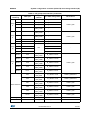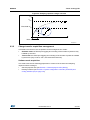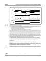
1
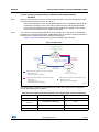
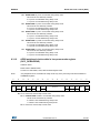
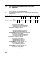
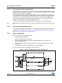
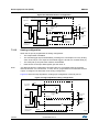
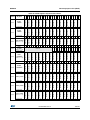
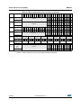
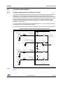
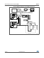
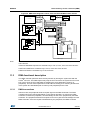
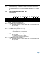
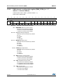
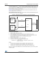
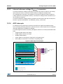
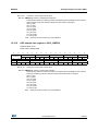
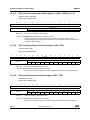
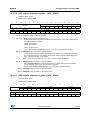
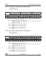
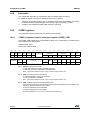
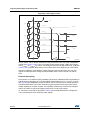
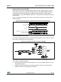
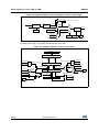
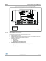
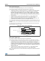
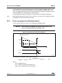
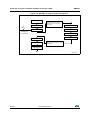
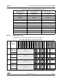
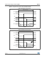
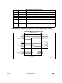
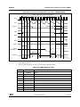
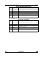
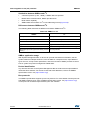
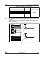
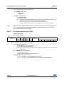
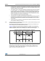
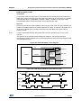
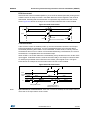
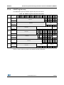
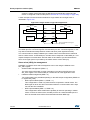
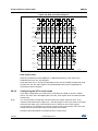
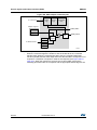
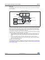
RM0038
7.3.4
General-purpose I/Os (GPIO)
I/O port data registers
Each GPIO has two 16-bit memory-mapped data registers: input and output data registers
(GPIOx_IDR and GPIOx_ODR). GPIOx_ODR stores the data to be output, it is read/write
accessible. The data input through the I/O are stored into the input data register
(GPIOx_IDR), a read-only register.
See Section 7.4.5: GPIO port input data register (GPIOx_IDR) (x = A..H) and Section 7.4.6:
GPIO port output data register (GPIOx_ODR) (x = A..H) for the register descriptions.
7.3.5
I/O data bitwise handling
The bit set reset register (GPIOx_BSRR) is a 32-bit register which allows the application to
set and reset each individual bit in the output data register (GPIOx_ODR). The bit set reset
register has twice the size of GPIOx_ODR.
To each bit in GPIOx_ODR, correspond two control bits in GPIOx_BSRR: BSRR(i) and
BSRR(i+SIZE). When written to 1, bit BSRR(i) sets the corresponding ODR(i) bit. When
written to 1, bit BSRR(i+SIZE) resets the ODR(i) corresponding bit.
Writing any bit to 0 in GPIOx_BSRR does not have any effect on the corresponding bit in
GPIOx_ODR. If there is an attempt to both set and reset a bit in GPIOx_BSRR, the set
action takes priority.
Using the GPIOx_BSRR register to change the values of individual bits in GPIOx_ODR is a
“one-shot” effect that does not lock the GPIOx_ODR bits. The GPIOx_ODR bits can always
be accessed directly. The GPIOx_BSRR register provides a way of performing atomic
bitwise handling.
There is no need for the software to disable interrupts when programming the GPIOx_ODR
at bit level: it is possible to modify one or more bits in a single atomic AHB write access.
7.3.6
GPIO locking mechanism
It is possible to freeze the GPIO control registers by applying a specific write sequence to
the GPIOx_LCKR register. The frozen registers are GPIOx_MODER, GPIOx_OTYPER,
GPIOx_OSPEEDR, GPIOx_PUPDR, GPIOx_AFRL and GPIOx_AFRH.
To write the GPIOx_LCKR register, a specific write / read sequence has to be applied. When
the right LOCK sequence is applied to bit 16 in this register, the value of LCKR[15:0] is used
to lock the configuration of the I/Os (during the write sequence the LCKR[15:0] value must
be the same). When the LOCK sequence has been applied to a port bit, the value of the port
bit can no longer be modified until the next MCU or peripheral reset. Each GPIOx_LCKR bit
freezes the corresponding bit in the control registers (GPIOx_MODER, GPIOx_OTYPER,
GPIOx_OSPEEDR, GPIOx_PUPDR, GPIOx_AFRL and GPIOx_AFRH).
The LOCK sequence (refer to Section 7.4.8: GPIO port configuration lock register
(GPIOx_LCKR) (x = A..H)) can only be performed using a word (32-bit long) access to the
GPIOx_LCKR register due to the fact that GPIOx_LCKR bit 16 has to be set at the same
time as the [15:0] bits.
For more details please refer to LCKR register description in Section 7.4.8: GPIO port
configuration lock register (GPIOx_LCKR) (x = A..H).
DocID15965 Rev 13
177/901
190