1
5
Functional Description
5.1
Block Diagram
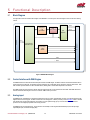
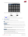
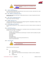
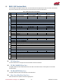
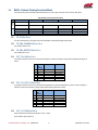
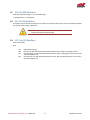
The Figure below shows the functional block diagram of the DM35425. The various parts of the block diagram are discussed in the following
sections.
PGA
(0.5,1,2,4,8)
AIN 31
Input
Multiplexer
PCIe x1
Control Interface
With DMA Engine
I/O Connector
PCIe Bus
…
AIN 0
Analog input:
12 bit
@1.25MSPS
Analog Output:
12 bit @
200KHz
…
DIO0
DIO31
Figure 8: DM35425 Block Diagram
5.2
Control Interface with DMA Engine
The DM35425 features a FPGA with a built in PCI Express interface and DMA engine. The FPGA controls all communication between the bus
and the control logic on the board. The FPGA also features small FIFOs for use with DMA, which is needed for continuous data transfer. Each
DAC and ADC is provided with its own FIFO and DMA channel, allowing them to transfer data independent of one another.
Each DMA channel can be programmed to transfer data from FPGA to PCIe bus or from the PCIe bus to the FPGA. Each DMA channel also
features a 64-bit PCI addressing and can access a maximum 16MB of memory for buffers.
5.3
Analog input
The DM35425 has 16 differential or 32 single-end channel inputs muxed to a single 12 bit SAR ADC converter, to provide high speed and high
digital resolution of the analog input. The ADC converter has a max throughput of 1.25MHz (1 Channel). Refer to Equation 1 below to calculate
max sampling rate. The high input impedance, low distortion, low noise operation design give you accurate results. The DM35425 also
provides ±12V overvoltage input protection to the analog connector.
The DM35425 has a programmable input. This provides the user the ability to select single-ended/differential input, full-scale input range,
unipolar/bipolar input, and channel sampling delay.
RTD Embedded Technologies, Inc. | www.rtd.com
24
DM35425HR User’s Manual