1
6.6
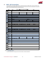
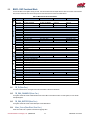
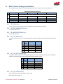
BAR2 – External Clocking Functional Block
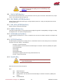
This function block provides an interface to the External Clocking. It is used to input or output the source of the CLK_SRC_GLBn.
Header
Table 22:External Clocking Functional Block
6.6.1
Offset
FB + 0x00
0x03
FB_ID
0x02
0x01
0x00
FB + 0x04
FB_DMA_BUFFERS
FB_DMA_CHANNELS
Reserved
Reserved
FB + 0x08
FB + 0x0C
FB + 0x10
FB + 0x14
EXT_CLK_EDGE
EXT_CLK_PW5
EXT_CLK3_CFG
EXT_CLK7_CFG
EXT_CLK_DIR
EXT_CLK_PW4
EXT_CLK2_CFG
EXT_CLK6_CFG
EXT_CLK_GATE_IN
EXT_CLK_PW3
EXT_CLK_PW7
EXT_CLK5_CFG
EXT_CLK_IN
EXT_CLK_PW2
EXT_CLK_PW6
EXT_CLK4_CFG
FB_ID (READ-ONLY)
This is the functional block ID. This register should read 0x00000002 for the External Clocking functional block.
6.6.2
FB_DMA_CHANNELS (READ -ONLY)
Has no DMA channels, reads 0
6.6.3
FB_DMA_BUFFERS (READ-ONLY)
Has no DMA buffers, reads 0
6.6.4
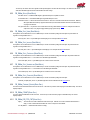
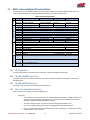
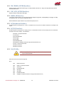
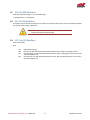
EXT_CLK_IN (READ-ONLY)
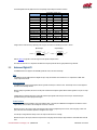
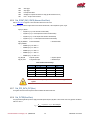
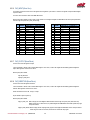
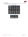
This register provides the current value on the External Clocking lines. The bits in the register correspond with the External Clocking pins as
follows:
Bit
CN3
Pin
Number
45
44
43
42
41
39
5
4
3
2
1
0
6.6.5
CLK_SRC_GLBn
Signal
7
6
5
4
3
2
EXT_CLK_7
EXT_CLK_6
EXT_CLK_5
EXT_CLK_4
EXT_CLK_3
EXT_CLK_2
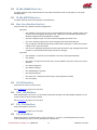
EXT_CLK_GATE_IN (READ ONLY)
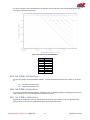
This register provides the current value on the External Clocking Gates lines. External Clocking Gates can only be used when inputting an
external clock. The bits in the register correspond with the External Clocking Gates pins as follows:
Bit
5
4
3
2
1
0
6.6.6
CN4
Pin
Number
45
44
43
42
41
39
CLK_SRC_GLBn
Signal
7
6
5
4
3
2
EXT_CLK_GATE7
EXT_CLK_GATE6
EXT_CLK_GATE5
EXT_CLK_GATE4
EXT_CLK_GATE3
EXT_CLK_GATE2
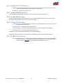
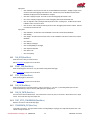
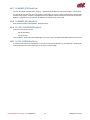
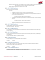
EXT_CLK_DIR (READ/WRITE)
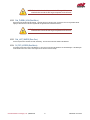
Selects the direction of the External Clocking bits. 0=input, 1=output.
All pins default to inputs at power-up.
RTD Embedded Technologies, Inc. | www.rtd.com
51
DM35425HR User’s Manual