1
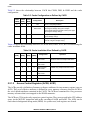
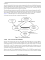
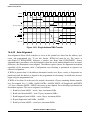
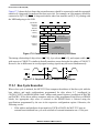
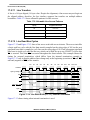
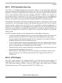
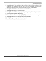
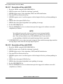
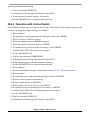
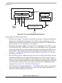
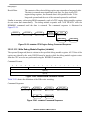
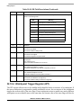
Data Transfer Operation
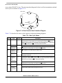
System
MCF5235
1.
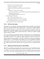
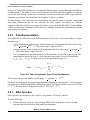
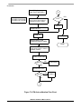
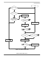
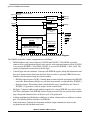
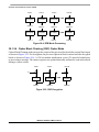
Set R/W to write
2.
Place address on A[31:0]
3.
Assert TIP and TSIZ[1:0]
4.
Assert TS
5.
Place data on D[31:0]
6.
Negate TS
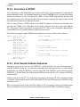
1.
Sample TA low
2.
Stop driving data from D[31:0]
1.
Start next cycle
1.
Decode address
2.
Store data on D[31:0]
3.
Assert TA
1.
Negate TA
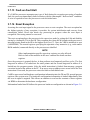
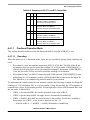
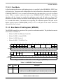
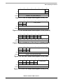
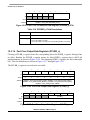
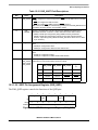
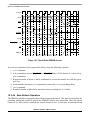
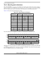
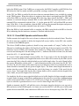
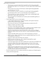
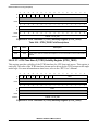
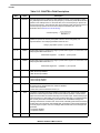
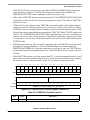
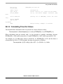
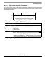
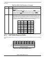
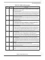
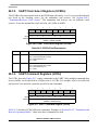
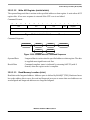
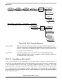
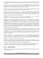
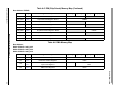
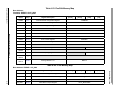
Figure 17-7. Write Cycle Flowchart
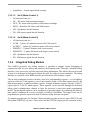
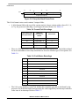
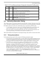
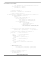
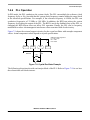
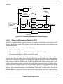
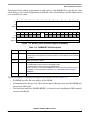
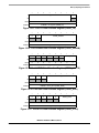
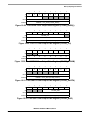
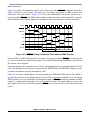
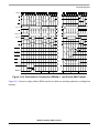
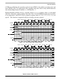
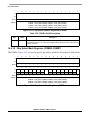
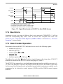
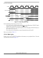
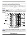
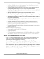
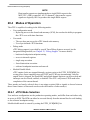
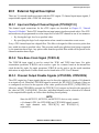
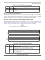
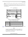
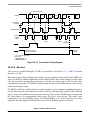
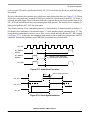
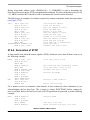
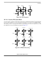
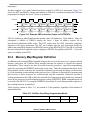
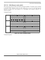
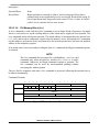
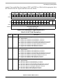
The write cycle timing diagram is shown in Figure 17-8.
S0
S1
S2
S3
S4
S5
CLKOUT
A[31:0], TSIZ[1:0]
R/W
TIP
TS
CSn, BSn
D[31:0]
Write
TA
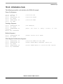
Figure 17-8. Basic Write Bus Cycle
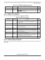
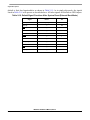
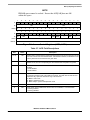
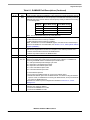
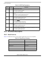
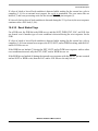
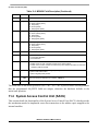
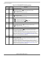
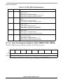
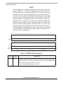
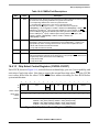
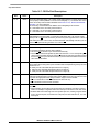
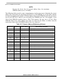
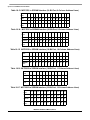
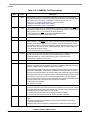
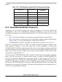
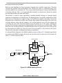
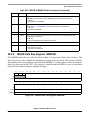
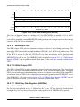
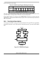
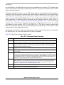
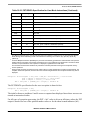
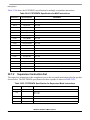
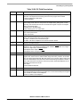
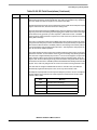
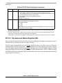
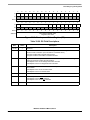
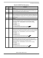
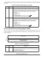
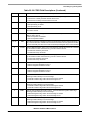
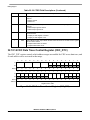
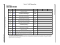
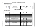
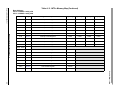
Table 17-4 describes the six states of a basic write cycle.
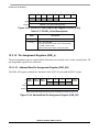
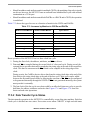
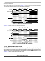
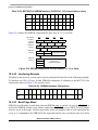
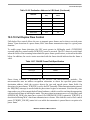
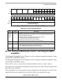
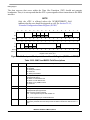
17.5.5 Fast Termination Cycles
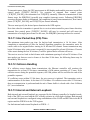
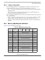
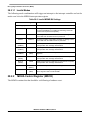
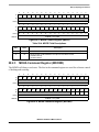
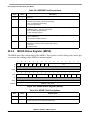
Two clock cycle transfers are supported on the MCF5235 bus. In most cases, this is impractical to
use in a system because the termination must take place in the same half-clock during which TS
is asserted. As this is atypical, it is not referred to as the zero-wait-state case but is called the
fast-termination case. Fast termination cycles occur when the external device or memory asserts
TA less than one clock after TS is asserted. This means that the MCF5235 samples TA on the rising
MCF5235 Reference Manual, Rev. 2
Freescale Semiconductor
17-9