1
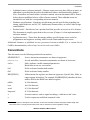
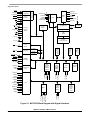
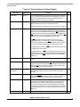
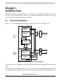
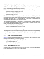
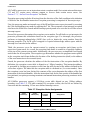
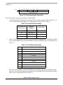
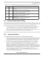
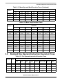
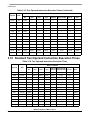
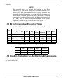
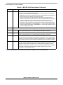
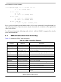
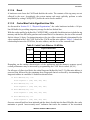
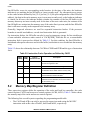
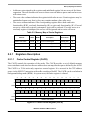
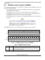
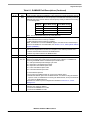
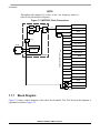
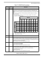
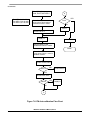
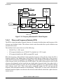
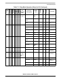
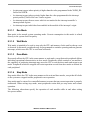
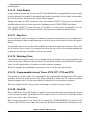
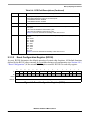
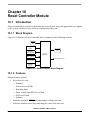
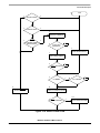
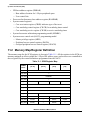
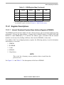
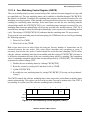
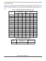
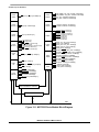
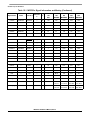
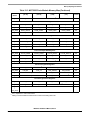
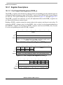
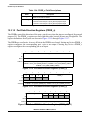
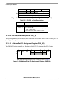
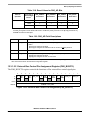
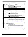
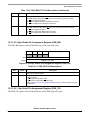
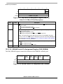
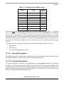
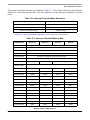
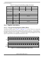
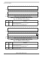
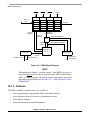
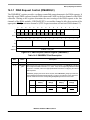
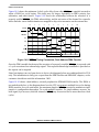
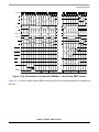
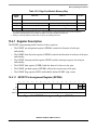
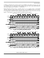
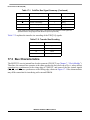
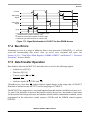
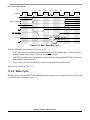
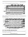
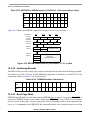
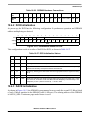
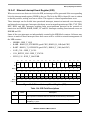
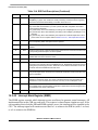
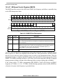
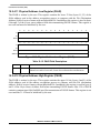
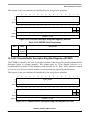
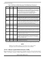
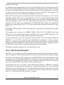
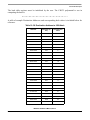
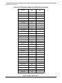
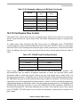
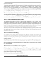
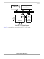
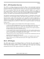
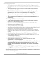
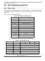
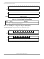
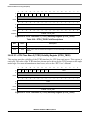
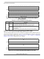
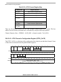
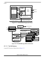
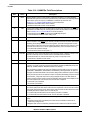
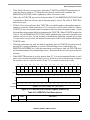
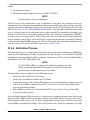
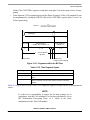
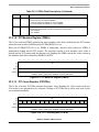
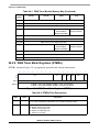
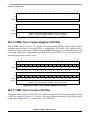
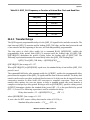
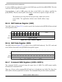
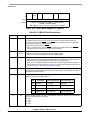
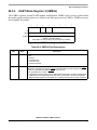
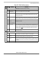
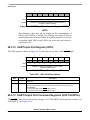
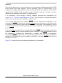
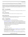
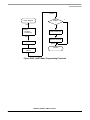
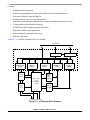
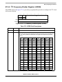
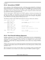
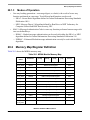
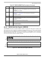
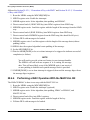
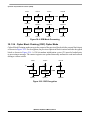
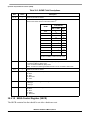
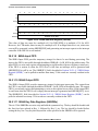
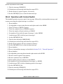
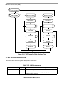
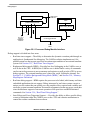
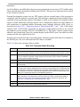
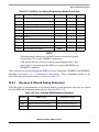
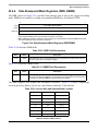
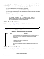
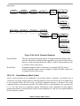
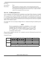
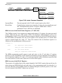
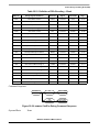
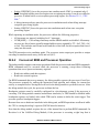
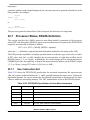
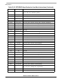
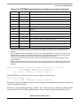
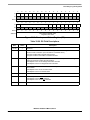
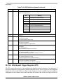
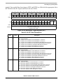
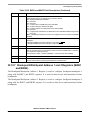
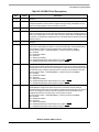
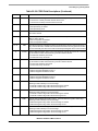
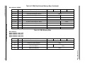
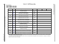
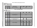
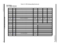
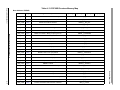
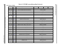
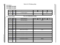
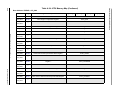
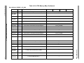
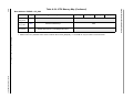
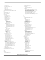
External Interface Module (EIM)
occur when CLKOUT is low. The state transition diagram for basic and fast termination read and
write cycles are shown in Figure 17-4.
Next Cycle
S0
S5
S1
Basic
Read/Write
S4
Fast
Termination
S2
Wait
States
S3
Figure 17-4. Data Transfer State Transition Diagram
Table 17-4 describes the states as they appear in subsequent timing diagrams.
Table 17-4. Bus Cycle States
State
Cycle
CLKOUT
Description
S0
All
High
The read or write cycle is initiated in S0. On the rising edge of CLKOUT, the
MCF5235 places a valid address on the address bus and drives R/W high for a
read and low for a write, if it is not already in the appropriate state. The MCF5235
asserts TIP, TSIZ[1:0], and TS on the rising edge of CLKOUT.
S1
All
Low
The appropriate CSn, BSn, and OE signals assert on the CLKOUT falling edge.
S2
S3
Fast
Termination
TA must be asserted during S1. Data is made available by the external device and
is sampled on the rising edge of CLKOUT with TA asserted.
Read/write
High
(skipped fast
termination)
TS is negated on the rising edge of CLKOUT in S2.
Write
The data bus is driven out of high impedance as data is placed on the bus on the
rising edge of CLKOUT.
Read/write
(skipped for
fast
termination)
Low
Read
S4
All
Read
(including
fast-terminati
on)
The MCF5235 waits for TA assertion. If TA is not sampled as asserted before the
rising edge of CLKOUT at the end of the first clock cycle, the MCF5235 inserts wait
states (full clock cycles) until TA is sampled as asserted.
Data is made available by the external device on the falling edge of CLKOUT and
is sampled on the rising edge of CLKOUT with TA asserted.
High
The external device should negate TA.
The external device can stop driving data after the rising edge of CLKOUT.
However data could be driven through the end of S5.
MCF5235 Reference Manual, Rev. 2
17-6
Freescale Semiconductor