1
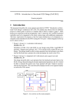
King Mongkut’s University of Technology Thonburi
Faculty of Engineering
Department of Electronic and Telecommunication Engineering
ENE/EIE 312 Electronic Engineering Laboratory,
for 3rd year students of the Electrical Communication and Electronic Engineering Curriculum
Experiment 12: Electronic Design Automation (EDA) for Digital Design Using VHDL and FPGA
Objectives
1. To understand modern digital design methodology based on VHDL and FPGA.
2. To practice using Electronic Design Automation (EDA) tools including simulation, synthesis, and
implementation for digital design based on VHDL and FPGA.
Background Theory
Due to the advance of the IC technology, digital systems have become very complex. As a result,
digital design has become very involved process and advance tools are required. Modern digital design relies on a set of software programs collectively called EDA tools by which a model of a digital
system can be simulated or synthesized before being implemented into a real hardware such as
FPGA (Field Programmable Gate Array) chip for testing. A digital system is usually modeled using a
Hardware Description Language (HDL) such as VHDL (which stands for Very-high speed IC HDL) and
Verilog. Figure 12.1 shows an FPGA-based digital system design methodology, which includes the
following steps.
Figure 12.1 FPGA-based digital design methodology
In-charge Faculty Staff: Asst. Prof. Dr. Pinit Kumhom
12-1
King Mongkut’s University of Technology Thonburi
Faculty of Engineering
Department of Electronic and Telecommunication Engineering
ENE/EIE 312 Electronic Engineering Laboratory,
for 3rd year students of the Electrical Communication and Electronic Engineering Curriculum
Step 1a: System Modeling Using HDL
The goal in this step is to model the system using a HDL (in our case, we use VHDL). The job of designer is to specify the system and use VHDL to describe it in such a way that it can be synthesized
into a logic-level circuit later. Most of designer’s time should be spent in this step whereas VHDL
programs are produced as needed. Knowledge and skills needed in this step are VHDL, fundamental
digital system, text editor, and problem-solving skills. In this laboratory, we’ll use three digital systems as examples.
Simulation
Experiment
A stimulus
e.g. signal
generators
Circuit’s
input
testbench
Output observer
e.g. logic
analyzer
A physical
Circuit
(hardware)
Circuit’s
output
A stimulus generator or
test vector generator
- VHDL utility routines
Wave editors
Circuit’s
input
(a) Testing by experiment
Output observer
- VHDL utility
routines
Human
A model of
the hardware
(e.g. VHDL code)
Circuit’s
output
(b) Verifying by simulation
Figure 12. 2 Concept of testbench program of verification using simulation
Step 1b: Testbench Program
The goal is this step is to write a VHDL program called “testbench”, which will be used in the functional simulation step. A testbench is a VHDL program in which a design under test (DUT) that is
modeled in Step 1a is instantiated. The input ports of the DUT are fed by a set of test vectors that
either stored or generated inside the testbench. The DUT’s output ports are compared with the correct responses stored inside the testbench. Figure 12.2 shows the concept of testbench.
In-charge Faculty Staff: Asst. Prof. Dr. Pinit Kumhom
12-2
King Mongkut’s University of Technology Thonburi
Faculty of Engineering
Department of Electronic and Telecommunication Engineering
ENE/EIE 312 Electronic Engineering Laboratory,
for 3rd year students of the Electrical Communication and Electronic Engineering Curriculum
Step 2: Functional Simulation
The goal in this step is to verify that the designed system (the VHDL model from Step 1a) is working
correctly based on its function specification. For example, if the designed system is a 4-bit binary
adder, it must add two numbers together correctly. This is prepared during the testbench coding in
Step 1b. In other words, the appropriated test vectors must be designed for verifying the system.
Once the test vectors are decided, they are integrated in the testbench. Therefore, in this step, a
designer basically setting up the simulation tool for the design under test, then, compile and run it.
Most works that needs to be done in this step occur when the VHDL codes contain errors, either
compile-time errors or run-time errors. Designer needs to correct the compile-time errors first before simulating the system. If all results are correct the designed system is good for the next step,
but if there exist error cases, designer needs to go back to Step 1a to correct the errors. These two
Steps should be repeated until no errors exist.
Step 3: Synthesis
The goal in this step is to synthesize the verified system into gate-level (or logic-level) circuit using a
synthesis tool. Unlike the simulation step, the testbench is not required in this step. The resulting
gate-level circuit is called “netllist”, which is usually written in a standard netlist format including
the HDL format.
Step 4: (Optional) Gate-level Simulation
There is a chance that the synthesized gate-level circuit may not work correctly. As a result, it
should be verified by simulation using the same testbench from Step 1b. However, in some cases
where the system is not complicated, we may skip this Step and go directly to the implementation
step.
Step 5: Implementation
In this step, the gate-level circuit will be mapped into the structure of the target hardware. For
FPGA implementation, the first step is to translate the gate-level circuit into FPGA structure, which is
arranged as an array of programmable or configurable logic blocks (CLBs) that are connected via
programmable switching blocks as shown in Figure 12.3. The result from the translation is a circuit
of the programmable units, which in turn will be placed to the target FPGA chip, then routing the
connections. Because of these placing and routing works, this step is also known as the “place and
route” step. The final result is called a configuration file and delay file that provides delay information of the system.
In-charge Faculty Staff: Asst. Prof. Dr. Pinit Kumhom
12-3
King Mongkut’s University of Technology Thonburi
Faculty of Engineering
Department of Electronic and Telecommunication Engineering
ENE/EIE 312 Electronic Engineering Laboratory,
for 3rd year students of the Electrical Communication and Electronic Engineering Curriculum
(a)
(b)
Figure 12.3 (a) General FPGA chip structure and (b) example of programmable or configurable logic
block (CLB)
Step 6: (Optional) Detail Simulation or Timing Analysis
Since the implementation step gives us the actual hardware structure and delay information, we
can simulate the system again to see not only does whether it works correctly or not but also the
timing. Usually, this simulation will take a longer time. Therefore, for small systems, we may skip
the step or in some cases, only the timing is analyzed to see whether or not it meets the requirement.
In-charge Faculty Staff: Asst. Prof. Dr. Pinit Kumhom
12-4
King Mongkut’s University of Technology Thonburi
Faculty of Engineering
Department of Electronic and Telecommunication Engineering
ENE/EIE 312 Electronic Engineering Laboratory,
for 3rd year students of the Electrical Communication and Electronic Engineering Curriculum
Step 7: Device Program
In this step, the configuration file is transferred or programmed into the FPGA chip via the JTAG
communication. There are two choices in this step. First, we program the configuration file directly
to the FPGA chip. However, this configuration will disappear when the power is off. Therefore, in
real application of FPGA, the configuration file is stored inn an EEPROM (or flash memory) that connects directly to the JTAG ports of the FPGA chip. Then, whenever the power is turned on, the prestored configuration file will be transferred into the FPGA chip.
Figure 12.4 FPGA Discovery III by APEX [2]
Step 8: Hardware Test
The final step is to test whether the actual hardware is working correctly as designed. Usually, a development board is required to perform this testing. In other words, the chip that was being programmed in the previous step is on a development board, which includes input devices such as
switches and output devices such as LED and 7-segment LED display. In testing, we must connect
the input ports of the design to input devices of the board and the output ports to the output deIn-charge Faculty Staff: Asst. Prof. Dr. Pinit Kumhom
12-5
King Mongkut’s University of Technology Thonburi
Faculty of Engineering
Department of Electronic and Telecommunication Engineering
ENE/EIE 312 Electronic Engineering Laboratory,
for 3rd year students of the Electrical Communication and Electronic Engineering Curriculum
vices. This should be done in the implementation step. Figure 12.4 shows a picture of development
board called “FPGA Discovery III” by APEX, Thailand.
Notes
Students are expected to study the attached material entitled “VHDL: A Walkthrough Tutorial” and the reference textbook. Also, a brief lecture will be carried out by the lab supervisor at the
beginning of the lab, and there may be a quiz on the topic at the beginning of the lab session.
Attachments
1. Pinit Kumhom, “Xilinx’s ISE and WebPack”, a laboratory note, ENE/EIE 312 Electronic Engineering
Lab., Department of Electronic and Telecommunication, Faculty of Engineering, KMUTT, 2555.
2. APEX, “Discovery III Development Board User Manual”, a technical manual,
http://www.ailogictechnology.com/download/FPGA%20Discovery%20III%20XC3S200F_F4%20Boar
d%20Manual.pdf
References
1. Wakerly, John, “Digital Design: Principle and Practices”, 4th Edition, Pearson International Edition,
2005.
2. Chu, Pong P., “RTL Hardware Design Using VHDL”, 1st edition, Wiley-Interscience, A John Wiley &
Sons, Inc., Publication, 2006.
Equipment and Devices
Items
Quantity
1. A PC computer with Xilinx’s Webpack software installed
1
2. FPGA development board
1
3. Digital Oscilloscope with logic analyzer
1
In-charge Faculty Staff: Asst. Prof. Dr. Pinit Kumhom
12-6
King Mongkut’s University of Technology Thonburi
Faculty of Engineering
Department of Electronic and Telecommunication Engineering
ENE/EIE 312 Electronic Engineering Laboratory,
for 3rd year students of the Electrical Communication and Electronic Engineering Curriculum
Procedure
Step 1: System Modeling (VHDL Coding) and Testbench program
In this experiment, students will have a chance to go through the design steps of modern digital
system design as shown in Fig. 12.1 using 3 examples as follows.
Figure 12.5 Specification of the 4-bit binary adder
Figure 12.6 Ripple carry 4-bit binary adder
In-charge Faculty Staff: Asst. Prof. Dr. Pinit Kumhom
12-7
King Mongkut’s University of Technology Thonburi
Faculty of Engineering
Department of Electronic and Telecommunication Engineering
ENE/EIE 312 Electronic Engineering Laboratory,
for 3rd year students of the Electrical Communication and Electronic Engineering Curriculum
Figure 12.7 VHDL code for ripple carry 4-bit binary adder
System 1: A 4-bit Binary Adder
A 4-bit binary adder is a system with two 4-bit inputs coded as binary number for representing natural number 0 to 15. In addition, another 1-bit input representing an external carry in whose value is
either 0 or 1 is added. The output is a 5-bit that stored the sum of the 3 inputs. Figure 12.5 shows
the specification of the system.
One way to design this 4-bit binary adder is to decompose the system into 4 1-bit adders,
called full adders, connected in cascade as shown in Figure 12.6. The VHDL program that model
this design is shown in Figure 12.7 in which the FA component is the full adder whose VHDL code is
shown in Figure 12.8.
In-charge Faculty Staff: Asst. Prof. Dr. Pinit Kumhom
12-8
King Mongkut’s University of Technology Thonburi
Faculty of Engineering
Department of Electronic and Telecommunication Engineering
ENE/EIE 312 Electronic Engineering Laboratory,
for 3rd year students of the Electrical Communication and Electronic Engineering Curriculum
Figure 12.8 A VHDL code for full adder
Notice that the first design of the 4-bit binary adder has the longest propagation delay equal to 4
(the number of bits). This is not good if the number of bits increases. This problem can be solved
with the “carry-look-ahead unit” or “fast-carry unit” that generates the carry of every bit. Fortunately, in some FPGA chips, such fast carry chain unit is integrated inside the chip. The first design may
not use the fast-carry chain because we synthesize (decompose) the system to be the ripple-carray
system. Therefore, to use the fast-carry unit, we will let the software tool does the synthesis by
modeling the system with high-level HDL as shown in Figure 12.9.
In-charge Faculty Staff: Asst. Prof. Dr. Pinit Kumhom
12-9
King Mongkut’s University of Technology Thonburi
Faculty of Engineering
Department of Electronic and Telecommunication Engineering
ENE/EIE 312 Electronic Engineering Laboratory,
for 3rd year students of the Electrical Communication and Electronic Engineering Curriculum
Figure 12.9 High-level VHDL code for 4-bit binary adder
Testbench for 4-bit binary adder
To verify whether a VHDL model of a system work correctly or not, we design a VHDL testbench
probram that includes the unit under test (UUT), the input vectors, and output monitoring. Figure
12.10 shows an example of testbench for the 4-bit binary adder.
The first part in the testbench is the instantiation of the unit under test, which must be declared as component in the archtecture’s declaration area.
The second part involves the test vectors. Notice that the input signals are declared as a, b,
ci and the output signals are s and co. Then, the test vectors, a, b and ci, are declared as constants
a_v, b_v, and ci_v, which are array of 8 values of a, b, and ci respectively. Also the corresponding
correct results are declared as constant s_v. In other word, in this example, we choose to store the
test vectors instead of generating them. Since we need to store a and b which is the
std_logic_vector(3 downto 0), we declare user-defined type as “input_array” and declared array of
s_v as the “output_array”.
The third part is the running mechanism using the process statement. In each round of the
process (each index value of index i), the input vectors are set (a => a_v(i), b => b_v(i), c => ci_v(i)).
Then, the statement “wait for 100 ns” means that the time scale moves 100 ns. Then, the output s
In-charge Faculty Staff: Asst. Prof. Dr. Pinit Kumhom
12-10
King Mongkut’s University of Technology Thonburi
Faculty of Engineering
Department of Electronic and Telecommunication Engineering
ENE/EIE 312 Electronic Engineering Laboratory,
for 3rd year students of the Electrical Communication and Electronic Engineering Curriculum
is compared with s_v(i) which is the correct answer. If the answer is not correct, the simulation will
stop, using the “assertion statement”; otherwise, the simulation continues.
Figure 12.10 Testbench for “add4”, the 4-bit binary adder
In-charge Faculty Staff: Asst. Prof. Dr. Pinit Kumhom
12-11
King Mongkut’s University of Technology Thonburi
Faculty of Engineering
Department of Electronic and Telecommunication Engineering
ENE/EIE 312 Electronic Engineering Laboratory,
for 3rd year students of the Electrical Communication and Electronic Engineering Curriculum
Figure 12.11 Functional block diagram of 4-bit binary counter
Figure 12.12 VHDL code for the 4-bit binary counter
In-charge Faculty Staff: Asst. Prof. Dr. Pinit Kumhom
12-12
King Mongkut’s University of Technology Thonburi
Faculty of Engineering
Department of Electronic and Telecommunication Engineering
ENE/EIE 312 Electronic Engineering Laboratory,
for 3rd year students of the Electrical Communication and Electronic Engineering Curriculum
System 2: 4-bit Counter
Counter is an important sequential module because it can be used as timer, which is required in
many applications. The basic functional block of a binary counter consists of a register, an incrementer and a multiplexor (MUX) as shown in Figure 12.11. A VHDL program of a 4-bit binary counter
(cyclically count 0 to 15) is shown in Figure 12.12.
Figure 12.13 Testbench code for simulating the 4-bit binary counter
In-charge Faculty Staff: Asst. Prof. Dr. Pinit Kumhom
12-13
King Mongkut’s University of Technology Thonburi
Faculty of Engineering
Department of Electronic and Telecommunication Engineering
ENE/EIE 312 Electronic Engineering Laboratory,
for 3rd year students of the Electrical Communication and Electronic Engineering Curriculum
Testbench for the 4-bit counter
Verifying a counter is to check that it counts correctly. Figure 12.13 shows an example of such
testbench. Again, the unit under test (“count4” component) must be instantiated. Unlike the adder
testbench, we generated all input signals, including the clock signal (clk), the reset signal (rst_n) and
count control (count). Notice that we use one process to generate clock and the other to generate
rst_n and count.
(a) Block diagram of a 4-bit LFSR
(b) Gate-level circuit of the 4-bit LFSR
Figure 12.12 (a) Block diagram of the 4-bit LFSR (b) Gate-level circuit
System 3: 4-bit Linear Feedback Shift Register (LSFR)
Linear feedback shift registers (LSFR) are used mostly for implementing error-correcting codes.
Moreover, another major application of LFSR is to generate uniform pseudorandom numbers. Figure
12.12 shows the functional block diagram of the 4-bit LSFR that can generate 15 non-zero numbers
that look like random numbers. The VHDL code for the 4-bit LFSR is shown in Figure 12.13 with addition of inserting the zero so that all 16 numbers are generated and the count control (count).
In-charge Faculty Staff: Asst. Prof. Dr. Pinit Kumhom
12-14
King Mongkut’s University of Technology Thonburi
Faculty of Engineering
Department of Electronic and Telecommunication Engineering
ENE/EIE 312 Electronic Engineering Laboratory,
for 3rd year students of the Electrical Communication and Electronic Engineering Curriculum
Since the ports of the “lfsr4” and “count4” are the same and they both are a kind of counters,
they testbench is the same except the unit under test part of the testbench.
Figure 12.13 VHDL code for 4-bit LFSR with zero insertion and count control
Experiment 1: 4-bit ripple-carry binary adder
Function Simulation
1. Create a new directory in drive D with the name “S<m>G<n>” where m is chosen from 1, 2, 3 or
I depending on your class session and n is the number of your group; e.g. S1G1A = session 1
group 1A.
2. Open the Xilinx’s ISE program. Then, choose the “Create new project” menu to create a new
project. A pop-up menu similar to Figure 12.14 appears. Enter “ripple-adder” as the name and
click on the “…” on the right of the Location line to browse to the directory created in Step 1.
In-charge Faculty Staff: Asst. Prof. Dr. Pinit Kumhom
12-15
King Mongkut’s University of Technology Thonburi
Faculty of Engineering
Department of Electronic and Telecommunication Engineering
ENE/EIE 312 Electronic Engineering Laboratory,
for 3rd year students of the Electrical Communication and Electronic Engineering Curriculum
Figure 12.14 Example of the “Create new project” pop-up menu
Figure 12.15 Example of the “Project setting” pop-up menu
In-charge Faculty Staff: Asst. Prof. Dr. Pinit Kumhom
12-16
King Mongkut’s University of Technology Thonburi
Faculty of Engineering
Department of Electronic and Telecommunication Engineering
ENE/EIE 312 Electronic Engineering Laboratory,
for 3rd year students of the Electrical Communication and Electronic Engineering Curriculum
Click “Next. Then, the “Project setting” pop-up menu as shown in Figure 12.15 appears. Choose
the setting to be the same as those shown in Figure 12.15. After clicking “Next”, the summary
menu will show up. Click “Finish”.
Figure 12.16 The “Add copy files” button
3. Click on the icon “Add copy of files” (see Figure 12.16) for adding source files of the project, the
pop-up menu similar to Figure 12.17 appears.
Figure 12.17 Example of the “Add copy of files” pop-up menu
From the pop-up window, browse to the directory
“<shared directory>\src\binaryadder\ripple\” in the shared folder. Then, choose all files in the directory (see Figure 12.16). Click “Open”, then notice the change in the ISE.
4. Choose the “Simulation” view (see Figure 12.18). Then, compile the “add4_tb.vhd”. If there exists syntax errors correct them.
In-charge Faculty Staff: Asst. Prof. Dr. Pinit Kumhom
12-17
King Mongkut’s University of Technology Thonburi
Faculty of Engineering
Department of Electronic and Telecommunication Engineering
ENE/EIE 312 Electronic Engineering Laboratory,
for 3rd year students of the Electrical Communication and Electronic Engineering Curriculum
Figure 12.18 ISE’s Simulation View
5. Run the ISE simulation to simulate the “add4_tb’. After the simulation is loaded, many windows
including the “Instance and Process”, the “Simulation objects”, the “waveform” and the “Console” windows show up inside the same frame. The “waveform” window (the one with the black
background) plots signal values against the hardware time (the horizontal axis), which is an imaginary time under which the hardware under test is assumed to be working.
type restart <enter> in the “command” window (the one with “#Isim” cursor), which
order the simulation to reset the hardware time to zero (current time = 0). Then
type run <Max_time> <enter> for running the simulation, where “Max_time” is the
hardware time for the simulation to progress from the current time. For example, run 1000 ns
to order the simulation to execute until the hardware time reaches “current time” + 1000 ns.
In-charge Faculty Staff: Asst. Prof. Dr. Pinit Kumhom
12-18
King Mongkut’s University of Technology Thonburi
Faculty of Engineering
Department of Electronic and Telecommunication Engineering
ENE/EIE 312 Electronic Engineering Laboratory,
for 3rd year students of the Electrical Communication and Electronic Engineering Curriculum
Figure 12.19 Example of the ISim’s window display
If the simulation exits before it reaches the 1000 ns time, it means that there exists a wrong result at the time the simulation exit; otherwise, all results are corrected. An error can be either
that the “wrong answer” is stored or that the output response is wrong. If no error is found, click
the “full view” button (Move the mouse pointer to a button to see what it is. The “full view”
button is in the middle of the window). Figure 12.19 shows the full view of the simulation results
of the “add4” after the run 1000 ns command when there is no error.
Synthesis and Implementation
6. Choose the “Implementation” button on the top of the “ISE” window. The ISE window should
change to something similar to Figure 12.20.
7. In the process window, expand the “User constraints” button in the window. Then, double click
to run the “I/O Pin Planning (PlanAhead) – Pre Synthesis”. The PlanAhead’s window similar to
Figure 12.21 should show up. (You might need to wait for quite a long time.) Edit the Ports’ site
of all ports to the appropriate pins, which must be planned ahead by consulting the development board’s manual (Attachment 2). For the pin setup that shows in Figure 12.21, we use the
“DIP” switch number 1, 2, 3, 4 for the input port “a”, the “DIP SW” number 5 – 8 for the input
port “b”, the “PB1” switch for the input port “ci”, and the LED number L7, L3, L2, L1, L0 for the
output port “s”.
8. Run the “Synthesis”. If there is no error, record the synthesis report especially the “device’s utilization” part.
9. Run the “Implement”. If there is no error, record the device’s utilization again. Compare it with
one from the synthesis step.
In-charge Faculty Staff: Asst. Prof. Dr. Pinit Kumhom
12-19
King Mongkut’s University of Technology Thonburi
Faculty of Engineering
Department of Electronic and Telecommunication Engineering
ENE/EIE 312 Electronic Engineering Laboratory,
for 3rd year students of the Electrical Communication and Electronic Engineering Curriculum
Figure 12.20 Example of the ISE Implementation view
Figure 12.21 PlanAhead’s window for editing the Pin’s assignment for the I/O ports
In-charge Faculty Staff: Asst. Prof. Dr. Pinit Kumhom
12-20
King Mongkut’s University of Technology Thonburi
Faculty of Engineering
Department of Electronic and Telecommunication Engineering
ENE/EIE 312 Electronic Engineering Laboratory,
for 3rd year students of the Electrical Communication and Electronic Engineering Curriculum
10. Run “Generate Programming File”. The configuration file named as <design_name>.bit (e.g.
add4.bit) should be generated inside the project’s directory.
11. Run “Manage Configuration Project (iMPACT)”. The window similar to Figure 12.22 appears after
doubling on the “Boundary Scan”. Using the right click on the right sub-window to select “Initialize the Chain”, we get the JTAG chain as shown in Figure 12.23. (Choose cancel when there is a
pop-up menu appears).
12. Right click on the “XC3S200” device. Then, choosing the “Assign new configuration file”, the
window similar to Figure 12.24 appear. Browse to the project directory to chose the
<deign_name>.bit file. Click “OK”.
13. After the configuration has been assigned, right click on the “XC3S200” again. This time choose
“Program” to program the configuration file to the chip. After some time the “Program Successful” should appear. If the program is failed consult the Lab’s supervisor.
14. Perform the experiment to test whether or not the hardware is working correctly.
Experiment 2: 4-bit binary adder (high-level VHDL code)
Repeat Step 2 – 14 but name the project “high-level-adder” and use the source files from the directory “<shared directory>\src\binaryadder\high-level\” instead.
Experiment 3: 4-bit binary counter
Repeat Step 2 – 14 but name the project “counter” and use the source files from the directory
“<shared directory>\src\counter\” instead.
Experiment 4: 4-bit LFSR
Repeat Step 2 – 14 but name the project “lfsr” and use the source files from the directory
“<shared directory>\src\lfsr\” instead.
Points of Discussion
1. Explain in your own words what you have learnt from this set of experiments in term of
VHDL modeling, design methodology, EDA tools, development boards, etc.
2. Discuss the differences between the simulation and the actual testing of hardware.
3. Discuss the differences between the simulation and synthesis.
4. Discuss the differences between the synthesis results and the implementation results.
5. Consult the manual of the XC3S200 to learn more about the FPGA chip using in this experiment, and discuss it in the report.
In-charge Faculty Staff: Asst. Prof. Dr. Pinit Kumhom
12-21
King Mongkut’s University of Technology Thonburi
Faculty of Engineering
Department of Electronic and Telecommunication Engineering
ENE/EIE 312 Electronic Engineering Laboratory,
for 3rd year students of the Electrical Communication and Electronic Engineering Curriculum
Figure 12.22 Example of the iMPACT window
Figure 12.23 The iMPACT window showing the JTAG chain of the Discovery III board
In-charge Faculty Staff: Asst. Prof. Dr. Pinit Kumhom
12-22