1
SAFETY PRECAUTIONS
(Read these precautions before using this product.)
Before using products introduced in this publication, please read relevant manuals and replacement
handbooks carefully and pay full attention to safety to handle the product correctly.
In this publication, the safety precautions are classified into two levels:
"
WARNING" and "
CAUTION".
WARNING
Indicates that incorrect handling may cause hazardous conditions,
resulting in death or severe injury.
CAUTION
Indicates that incorrect handling may cause hazardous conditions,
resulting in minor or moderate injury or property damage.
Under some circumstances, failure to observe the precautions given under "
serious consequences.
CAUTION" may lead to
Observe the precautions of both levels because they are important for personal and system safety.
Make sure that the end users read this publication and keep it in a safe place for future reference.
[Design Precautions]
WARNING
● Configure safety circuits external to the programmable controller to ensure that the entire system
operates safely even when a fault occurs in the external power supply or the programmable
controller. Failure to do so may result in an accident due to an incorrect output or malfunction.
(1) Configure external safety circuits, such as an emergency stop circuit, protection circuit, and
protective interlock circuit for forward/reverse operation or upper/lower limit positioning.
(2) When the programmable controller detects the following problems,
it will stop calculation and turn off all outputs in the case of (a).
In the case of (b), it will hold or turn off all outputs according to the parameter setting.
Note that the A series module will turn off the output in either of cases (a) and (b).
(a) The power supply module has over current
protection equipment and over voltage
protection equipment.
(b) The CPU module self-diagnosis functions, such
as the watchdog timer error, detect problems.
Q series module
A series module
Output OFF
Output OFF
Hold or turn off all output
according to the parameter
setting.
Output OFF
All outputs may turn on when an error occurs in the part, such as I/O control part, where the CPU
module cannot detect any error. To ensure safety operation in such a case, provide a safety
mechanism or a fail-safe circuit external to the programmable controller. For a fail-safe circuit
example, refer to Chapter 10 LOADING AND INSTALLATION in the QCPU User's Manual
(Hardware Design, Maintenance and Inspection).
(3) Outputs may remain on or off due to a failure of an output module relay or transistor. Configure
an external circuit for monitoring output signals that could cause a serious accident.
A-1
[Design Precautions]
WARNING
● In an output module, when a load current exceeding the rated current or an overcurrent caused by a
load short-circuit flows for a long time, it may cause smoke and fire. To prevent this, configure an
external safety circuit, such as a fuse.
● Configure a circuit so that the programmable controller is turned on first and then the external power
supply.
If the external power supply is turned on first, an accident may occur due to an incorrect output or
malfunction.
● For the operating status of each station after a communication failure, refer to relevant manuals for
the network.
Incorrect output or malfunction due to a communication failure may result in an accident.
● When changing data of the running programmable controller from a peripheral connected to the
CPU module or from a personal computer connected to an intelligent function module/special
function module, configure an interlock circuit in the sequence program to ensure that the entire
system will always operate safely.
For program modification and operating status change, read relevant manuals carefully and ensure
the safety before operation.
Especially, in the case of a control from an external device to a remote programmable controller,
immediate action cannot be taken for a problem on the programmable controller due to a
communication failure.
To prevent this, configure an interlock circuit in the sequence program, and determine corrective
actions to be taken between the external device and CPU module in case of a communication
failure.
CAUTION
● Do not install the control lines or communication cables together with the main circuit lines or power
cables.
Keep a distance of 100mm (3.94 inches) or more between them.
Failure to do so may result in malfunction due to noise.
● When a device such as a lamp, heater, or solenoid valve is controlled through an output module, a
large current (approximately ten times greater than normal) may flow when the output is turned from
off to on.
Take measures such as replacing the module with one having a sufficient current rating.
● After the CPU module is powered on or is reset, the time taken to enter the RUN status varies
depending on the system configuration, parameter settings, and/or program size. Design circuits so
that the entire system will always operate safely, regardless of the time.
A-2
[Installation Precautions]
CAUTION
● Use the programmable controller in an environment that meets the general specifications in the
QCPU User's Manual (Hardware Design, Maintenance and Inspection).
Failure to do so may result in electric shock, fire, malfunction, or damage to or deterioration of the
product.
● To mount the module, while pressing the module mounting lever located in the lower part of the
module, fully insert the module fixing projection(s) into the hole(s) in the base unit and press the
module until it snaps into place.
Incorrect mounting may cause malfunction, failure or drop of the module.
When using the programmable controller in an environment of frequent vibrations, fix the module
with a screw.
Tighten the screw within the specified torque range.
Undertightening can cause drop of the screw, short circuit or malfunction.
Overtightening can damage the screw and/or module, resulting in drop, short circuit, or malfunction.
● When using an extension cable, connect it to the extension cable connector of the base unit securely.
Check the connection for looseness.
Poor contact may cause incorrect input or output.
● When using a memory card, fully insert it into the memory card slot.
Check that it is inserted completely.
Poor contact may cause malfunction.
● Shut off the external power supply for the system in all phases before mounting or removing the
module. Failure to do so may result in damage to the product.
A module can be replaced online (while power is on) on any MELSECNET/H remote I/O station or in
the system where a CPU module supporting the online module change function is used.
Note that there are restrictions on the modules that can be replaced online, and each module has its
predetermined replacement procedure.
For details, refer to the relevant sections in the QCPU User's Manual (Hardware Design,
Maintenance and Inspection) and in the manual for the corresponding module.
● Do not directly touch any conductive part of the module.
Doing so can cause malfunction or failure of the module.
A-3
[Wiring Precautions]
WARNING
● Shut off the external power supply for the system in all phases before wiring.
Failure to do so may result in electric shock or damage to the product.
● After wiring, attach the included terminal cover to the module before turning it on for operation.
Failure to do so may result in electric shock.
CAUTION
● Ground the FG and LG terminals to the protective ground conductor dedicated to the programmable
controller.
Failure to do so may result in electric shock or malfunction.
● Use applicable solderless terminals and tighten them within the specified torque range. If any spade
solderless terminal is used, it may be disconnected when the terminal screw comes loose, resulting
in failure.
● Check the rated voltage and terminal layout before wiring to the module, and connect the cables
correctly.
Connecting a power supply with a different voltage rating or incorrect wiring may cause a fire or
failure.
● Connectors for external connection must be crimped or pressed with the tool specified by the
manufacturer, or must be correctly soldered.
Incomplete connections could result in short circuit, fire, or malfunction.
● Tighten the terminal screw within the specified torque range.
Undertightening can cause short circuit, fire, or malfunction.
Overtightening can damage the screw and/or module, resulting in drop, short circuit, or malfunction.
● Prevent foreign matter such as dust or wire chips from entering the module.
Such foreign matter can cause a fire, failure, or malfunction.
● A protective film is attached to the top of the module to prevent foreign matter, such as wire chips,
from entering the module during wiring.
Do not remove the film during wiring.
Remove it for heat dissipation before system operation.
● Mitsubishi programmable controllers must be installed in control panels.
Connect the main power supply to the power supply module in the control panel through a relay
terminal block.
Wiring and replacement of a power supply module must be performed by maintenance personnel
who is familiar with protection against electric shock. (For wiring methods, refer to the QCPU User's
Manual (Hardware Design, Maintenance and Inspection)).
A-4
[Startup and Maintenance Precautions]
WARNING
● Do not touch any terminal while power is on.
Doing so will cause electric shock.
● Correctly connect the battery connector.
Do not charge, disassemble, heat, short-circuit, solder, or throw the battery into the fire.
Doing so will cause the battery to produce heat, explode, or ignite, resulting in injury and fire.
● Shut off the external power supply for the system in all phases before cleaning the module or
retightening the terminal screws or module fixing screws.
Failure to do so may result in electric shock.
Undertightening the terminal screws can cause short circuit or malfunction.
Overtightening can damage the screw and/or module, resulting in drop, short circuit, or malfunction.
CAUTION
● Before performing online operations (especially, program modification, forced output, and operation
status change) for the running CPU module from the peripheral connected, read relevant manuals
carefully and ensure the safety.
Improper operation may damage machines or cause accidents.
● Do not disassemble or modify the modules.
Doing so may cause failure, malfunction, injury, or a fire.
● Use any radio communication device such as a cellular phone or PHS (Personal Handy-phone
System) more than 25cm (9.85 inches) away in all directions from the programmable controller.
Failure to do so may cause malfunction.
● Shut off the external power supply for the system in all phases before mounting or removing the
module. Failure to do so may cause the module to fail or malfunction.
A module can be replaced online (while power is on) on any MELSECNET/H remote I/O station or in
the system where a CPU module supporting the online module change function is used.
Note that there are restrictions on the modules that can be replaced online, and each module has its
predetermined replacement procedure.
For details, refer to the relevant sections in the QCPU User's Manual (Hardware Design,
Maintenance and Inspection) and in the manual for the corresponding module.
● After the first use of the product, do not mount/remove the module to/from the base unit, and the
terminal block to/from the module more than 50 times (IEC 61131-2 compliant) respectively.
Exceeding the limit of 50 times may cause malfunction.
● Do not drop or apply shock to the battery to be installed in the module.
Doing so may damage the battery, causing the battery fluid to leak inside the battery.
If the battery is dropped or any shock is applied to it, dispose of it without using.
● Before handling the module, touch a grounded metal object to discharge the static electricity from
the human body.
Failure to do so may cause the module to fail or malfunction.
A-5
[Disposal Precautions]
CAUTION
● When disposing of this product, treat it as industrial waste.
When disposing of batteries, separate them from other wastes according to the local regulations.
(For details of the battery directive in EU member states, refer to the QCPU User's Manual
(Hardware Design, Maintenance and Inspection).)
[Transportation Precautions]
CAUTION
● When transporting lithium batteries, follow the transportation regulations.
(For details of the regulated models, refer to the QCPU User's Manual (Hardware Design,
Maintenance and Inspection).)
A-6
CONDITIONS OF USE FOR THE PRODUCT
(1) Mitsubishi programmable controller ("the PRODUCT") shall be used in conditions;
i) where any problem, fault or failure occurring in the PRODUCT, if any, shall not lead to any major
or serious accident; and
ii) where the backup and fail-safe function are systematically or automatically provided outside of
the PRODUCT for the case of any problem, fault or failure occurring in the PRODUCT.
(2) The PRODUCT has been designed and manufactured for the purpose of being used in general
industries.
MITSUBISHI SHALL HAVE NO RESPONSIBILITY OR LIABILITY (INCLUDING, BUT NOT
LIMITED TO ANY AND ALL RESPONSIBILITY OR LIABILITY BASED ON CONTRACT,
WARRANTY, TORT, PRODUCT LIABILITY) FOR ANY INJURY OR DEATH TO PERSONS OR
LOSS OR DAMAGE TO PROPERTY CAUSED BY the PRODUCT THAT ARE OPERATED OR
USED IN APPLICATION NOT INTENDED OR EXCLUDED BY INSTRUCTIONS, PRECAUTIONS,
OR WARNING CONTAINED IN MITSUBISHI'S USER, INSTRUCTION AND/OR SAFETY
MANUALS, TECHNICAL BULLETINS AND GUIDELINES FOR the PRODUCT.
("Prohibited Application")
Prohibited Applications include, but not limited to, the use of the PRODUCT in;
• Nuclear Power Plants and any other power plants operated by Power companies, and/or any
other cases in which the public could be affected if any problem or fault occurs in the PRODUCT.
• Railway companies or Public service purposes, and/or any other cases in which establishment of
a special quality assurance system is required by the Purchaser or End User.
• Aircraft or Aerospace, Medical applications, Train equipment, transport equipment such as
Elevator and Escalator, Incineration and Fuel devices, Vehicles, Manned transportation,
Equipment for Recreation and Amusement, and Safety devices, handling of Nuclear or
Hazardous Materials or Chemicals, Mining and Drilling, and/or other applications where there is a
significant risk of injury to the public or property.
Notwithstanding the above, restrictions Mitsubishi may in its sole discretion, authorize use of the
PRODUCT in one or more of the Prohibited Applications, provided that the usage of the PRODUCT
is limited only for the specific applications agreed to by Mitsubishi and provided further that no
special quality assurance or fail-safe, redundant or other safety features which exceed the general
specifications of the PRODUCTs are required. For details, please contact the Mitsubishi
representative in your region.
A-7
REVISIONS
* The handbook number is given on the bottom left of the back cover.
Print Date
Nov., 2011
* Handbook Number
L(NA)-08219ENG-A
Revision
First edition
Japanese Handbook Version L-08209
This handbook confers no industrial property rights or any rights of any other kind, nor does it confer any patent licenses.
Mitsubishi Electric Corporation cannot be held responsible for any problems involving industrial property rights which may
occur as a result of using the contents noted in this handbook.
© 2011 MITSUBISHI ELECTRIC CORPORATION
A-8
CONTENTS
SAFETY PRECAUTIONS ................................................................................................................................A - 1
CONDITIONS OF USE FOR THE PRODUCT .................................................................................................A - 7
REVISIONS ......................................................................................................................................................A - 8
GENERIC TERMS AND ABBREVIATIONS ................................................................................................... A - 13
CHAPTER 1 INTRODUCTION
1 - 1 to 1 - 10
1.1
Considerations before Selection of Alternative Models for Replacement ........................................ 1 - 1
1.2
Suggestions for Transition from the AnS/QnAS (Small Type) Series to the Q Series ..................... 1 - 3
1.2.1
1.2.2
1.2.3
Advantages of transition to Q series ......................................................................................... 1 - 3
Suggestions for transition to Q series ....................................................................................... 1 - 4
Precautions for transition ........................................................................................................ 1 - 10
CHAPTER 2 REPLACEMENT OF CPU MODULE
2 - 1 to 2 - 32
2.1
List of Alternative Models of CPU Module ....................................................................................... 2 - 1
2.2
Comparison of CPU Module Specifications ..................................................................................... 2 - 8
2.3
Functional Comparison of CPU Module ........................................................................................ 2 - 16
2.3.1
2.3.2
2.4
Functional comparison between AnS series and Q series ..................................................... 2 - 16
Functional comparison between QnAS series and Q series .................................................. 2 - 20
Precautions for CPU Module Replacement ................................................................................... 2 - 24
2.4.1
2.4.2
2.4.3
2.4.4
2.4.5
2.4.6
Memory for CPU module ........................................................................................................ 2 - 24
Keyword registration and password registration ..................................................................... 2 - 27
Write during RUN ................................................................................................................... 2 - 27
Number of slots on the base unit ............................................................................................ 2 - 28
Base unit compatible with QCPU ........................................................................................... 2 - 30
Programming tool and connection cable for Q series CPU .................................................... 2 - 32
CHAPTER 3 REPLACEMENT OF I/O MODULE
3 - 1 to 3 - 89
3.1
List of Alternative Models of I/O Module .......................................................................................... 3 - 1
3.2
Comparison of I/O Module Specifications ...................................................................................... 3 - 13
3.2.1
3.2.2
3.2.3
3.2.4
3.2.5
3.3
Comparison of input module specifications ............................................................................ 3 - 13
Comparison of output module specifications .......................................................................... 3 - 47
Comparison of I/O combined module specifications .............................................................. 3 - 70
Comparison of interrupt module specifications ....................................................................... 3 - 86
Comparison of blank cover and dummy module specifications .............................................. 3 - 87
Precautions for I/O Module Replacement ...................................................................................... 3 - 88
CHAPTER 4 REPLACEMENT OF POWER SUPPLY MODULE
4 - 1 to 4 - 7
4.1
List of Alternative Models of Power Supply Module ......................................................................... 4 - 1
4.2
Comparison of Power Supply Module Specifications ...................................................................... 4 - 2
4.3
Precautions for Power Supply Module Replacement ...................................................................... 4 - 7
A-9
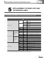
CHAPTER 5 REPLACEMENT OF BASE UNIT AND EXTENSION CABLE
5 - 1 to 5 - 16
5.1
List of Alternative Models of Base Unit and Extension Cable .......................................................... 5 - 1
5.2
Comparison of Base Unit and Extension Cable Specifications ........................................................ 5 - 3
5.2.1
5.2.2
5.3
Precautions for Replacement of Base Unit and Extension Cable .................................................... 5 - 7
5.3.1
5.3.2
5.4
Comparison of base unit specifications .................................................................................... 5 - 3
Comparison of extension cable specifications ......................................................................... 5 - 6
Precautions for replacement of base unit ................................................................................. 5 - 7
Precautions for replacement of extension cable ....................................................................... 5 - 7
QA(1S) Extension Base Unit ........................................................................................................... 5 - 8
5.4.1
5.4.2
5.4.3
5.4.4
5.4.5
5.4.6
5.4.7
QA(1S) extension base unit specifications ............................................................................... 5 - 8
Applicable QCPU ...................................................................................................................... 5 - 8
Extension cable ........................................................................................................................ 5 - 9
System configuration ................................................................................................................ 5 - 9
System equipment list ............................................................................................................. 5 - 11
I/O address for the QA(1S) extension base unit ..................................................................... 5 - 13
External dimensions ............................................................................................................... 5 - 15
CHAPTER 6 MEMORY AND BATTERY REPLACEMENT
6 - 1 to 6 - 2
6.1
List of Alternative Models for Memory .............................................................................................. 6 - 1
6.2
Precautions for Memory and Battery Replacement ......................................................................... 6 - 2
CHAPTER 7 REPLACEMENT OF PROGRAM
7.1
Program Replacement Procedure ................................................................................................... 7 - 4
7.1.1
7.1.2
7.1.3
7.1.4
7.2
7.2.2
7.2.3
7.2.4
7.2.5
A - 10
Replacing the AnSCPU with the QCPU .................................................................................. 7 - 31
Replacing the QnASCPU with the QCPU ............................................................................... 7 - 31
Replacement of Special Register .................................................................................................. 7 - 32
7.5.1
7.5.2
7.6
Conversion from AnSCPU to QCPU ....................................................................................... 7 - 27
Conversion from QnASCPU to QCPU .................................................................................... 7 - 29
Replacement of Special Relay ....................................................................................................... 7 - 31
7.4.1
7.4.2
7.5
List of instructions conversion from AnSCPU to QCPU
(Sequence/Basic/Application instructions) .............................................................................. 7 - 13
List of instruction conversion from AnSCPU to QCPU (Dedicated instructions) ..................... 7 - 18
Instructions that may need a replacement at instruction conversion from AnSCPU to QCPU 7 - 21
Instruction conversion from QnASCPU to QCPU ................................................................... 7 - 25
Instructions that may need a replacement after conversion from QnASCPU to QCPU ......... 7 - 26
Precautions for Replacement of Parameter ................................................................................... 7 - 27
7.3.1
7.3.2
7.4
Program conversion procedure from AnS/QnASCPU to QCPU ............................................... 7 - 4
Changing programmable controller type ................................................................................... 7 - 5
AnSCPU program conversion ratio ........................................................................................... 7 - 8
Reading (Reusing) other format files ...................................................................................... 7 - 10
Instruction Conversion ................................................................................................................... 7 - 13
7.2.1
7.3
7 - 1 to 7 - 48
Replacing the AnSCPU with the QCPU .................................................................................. 7 - 32
Replacing the QnASCPU with the QCPU ............................................................................... 7 - 32
Precautions for Replacement of the MELSAP-II with the MELSAP3 ............................................. 7 - 33
7.6.1
7.6.2
7.6.3
7.6.4
7.6.5
7.7
Starting SFC program ............................................................................................................. 7 - 33
Block information (SFC information device) ........................................................................... 7 - 33
Specifications comparison between MELSAP-II and MELSAP3 ............................................ 7 - 34
MELSAP3 specifications comparison between QnASCPU and QCPU .................................. 7 - 34
SFC diagram that cannot be read normally in another format ................................................ 7 - 35
Precautions for Program Replacement .......................................................................................... 7 - 36
7.7.1
7.7.2
7.7.3
7.7.4
7.7.5
7.7.6
7.7.7
7.7.8
7.7.9
7.7.10
7.7.11
7.7.12
List of applicable devices ........................................................................................................ 7 - 36
I/O control method .................................................................................................................. 7 - 39
Usable data format for instructions ......................................................................................... 7 - 39
Timer ...................................................................................................................................... 7 - 40
Counter ................................................................................................................................... 7 - 41
Display instructions ................................................................................................................. 7 - 41
Index register .......................................................................................................................... 7 - 41
Instructions where format is changed (Excluding AnUSCPU dedicated instructions) ............ 7 - 43
AnUSCPU dedicated instruction ............................................................................................. 7 - 44
Setting method when multiple sequence programs are created ............................................ 7 - 45
Precautions for file register replacement ................................................................................ 7 - 47
Boot run method (Writing programs to ROM) ......................................................................... 7 - 48
CHAPTER 8 EXTERNAL DIMENSIONS
8.1
8 - 1 to 8 - 3
Q Series External Dimensions and Mounting Dimensions .............................................................. 8 - 1
8.1.1
AnS/QnAS series external dimensions and mounting dimensions .......................................... 8 - 2
APPENDICES
App - 1 to App - 17
Appendix 1 Basic Model QCPU ............................................................................................................App - 1
Appendix 1.1
Appendix 1.2
Appendix 1.3
Major restrictions ....................................................................................................... App - 1
CPU module specifications comparison .................................................................... App - 3
CPU module functional comparison .......................................................................... App - 5
Appendix 2 Spare Parts Storage ........................................................................................................App - 11
Appendix 3 Related Manuals ..............................................................................................................App - 12
Appendix 3.1 Materials for replacement ........................................................................................App - 12
Appendix 3.2 AnS/QnAS series .....................................................................................................App - 13
Appendix 3.3 Q series ...................................................................................................................App - 15
Appendix 3.4 Programming tool ....................................................................................................App - 16
Appendix 3.5 Products manufactured by Mitsubishi Electric Engineering Co., Ltd. .......................App - 16
Appendix 3.6 Products manufactured by Mitsubishi Electric System & Service Co., Ltd. .............App - 16
A - 11
● For the products shown in handbooks for transition, Catalogue, and transition examples, refer to the
manuals for the relevant products and check the detailed specifications, precautions for use, and
restrictions before replacement.
For the products manufactured by Mitsubishi Electric Engineering Co., Ltd., Mitsubishi Electric System
& Service Co., Ltd., and other companies, refer to the catalogue for each product and check the
detailed specifications, precautions for use, and restrictions before use.
The manuals and catalogues for our products, products manufactured by Mitsubishi Electric
Engineering Co., Ltd., and Mitsubishi Electric System & Service Co., Ltd., are shown in Appendix of
each handbook for transition.
● For details on product compliance with the above standards, please contact your local Mitsubishi
Electric sales office or representative.
● Products shown in this handbook are subject to change without notice.
A - 12
GENERIC TERMS AND ABBREVIATIONS
Unless otherwise specified, this handbook uses the following generic terms and abbreviations.
Generic term/abbreviation
Series
A series
AnS series
A/AnS series
QnA series
QnAS series
QnA/QnAS series
A/AnS/QnA/QnAS series
Q series
CPU module type
CPU module
Basic model QCPU
High Performance model
QCPU
Process CPU
Redundant CPU
Description
Abbreviation for large types of Mitsubishi MELSEC-A series programmable controllers
Abbreviation for compact types of Mitsubishi MELSEC-A series programmable controllers
Generic term for A series and AnS series
Abbreviation for large types of Mitsubishi MELSEC-QnA series programmable controllers
Abbreviation for compact types of Mitsubishi MELSEC-QnA series programmable controllers
Generic term for QnA series and QnAS series
Generic term for A series, AnS series, QnA series, and QnAS series
Abbreviation for Mitsubishi MELSEC-Q series programmable controllers
Generic term for A series, AnS series, QnA series, QnAS series, and Q series CPU modules
Generic term for the Q00JCPU, Q00CPU, and Q01CPU
Generic term for the Q02CPU, Q02HCPU, Q06HCPU, Q12HCPU, and Q25HCPU
*
This handbook mainly explains about the Q02CPU, Q02HCPU, Q06HCPU, and Q12HCPU.
Generic term for the Q02PHCPU, Q06PHCPU, Q12PHCPU, and Q25PHCPU
Generic term for the Q12PRHCPU and Q25PRHCPU
Generic term for the Q00UJCPU, Q00UCPU, Q01UCPU, Q02UCPU, Q03UDCPU,
Q04UDHCPU, Q06UDHCPU, Q10UDHCPU, Q13UDHCPU, Q20UDHCPU, Q26UDHCPU,
Q03UDECPU, Q04UDEHCPU, Q06UDEHCPU, Q10UDEHCPU, Q13UDEHCPU,
Universal model QCPU
Q20UDEHCPU, Q26UDEHCPU, Q50UDEHCPU, and Q100UDEHCPU
*
This handbook mainly explains about the Q00UJCPU, Q00UCPU, Q01UCPU, Q02UCPU,
Q03UDCPU, Q04UDHCPU, and Q06UDHCPU, which can replace the AnS/QnAS series.
The specifications and functions of the Q10UDEHCPU to Q100UDEHCPU are the same as those of
the modules described above, although the program and memory capacities increase.
CPU module model
ACPU
AnSCPU
A/AnSCPU
AnNCPU
AnACPU
AnUCPU
AnN/AnACPU
AnN/AnA/AnSCPU
QnACPU
QnASCPU
QnA/QnASCPU
A/AnS/QnA/QnASCPU
QCPU
Generic term for MELSEC-A series programmable controller CPUs
Generic term for MELSEC-AnS series programmable controller CPUs
Generic term for MELSEC-A series and MELSEC-AnS series programmable controller CPUs
Generic term for the A1NCPU, A1NCPUP21/R21, A1NCPUP21-S3, A2NCPU, A2NCPU-S1,
A2NCPUP21/R21, A2NCPUP21/R21-S1, A2NCPUP21-S3(S4), A3NCPU, A3NCPUP21/R21,
and A3NCPUP21-S3
Generic term for the A2ACPU, A2ACPU-S1, A3ACPU, A2ACPUP21/R21, A2ACPUP21/R21S1, and A3ACPUP21/R21
Generic term for the A2UCPU, A2UCPU-S1, A3UCPU, A4UCPU, A2USCPU, A2USCPU-S1,
and A2USHCPU-S1
Generic term for the AnNCPU and AnACPU
Generic term for the AnNCPU, AnACPU, and AnSCPU
Generic term for MELSEC-QnA series programmable controller CPUs
Generic term for MELSEC-QnAS series programmable controller CPUs
Generic term for MELSEC-QnA series and MELSEC-QnAS series programmable controller
CPUs
Generic term for A series, AnS series, QnA series, and QnAS series programmable controller
CPUs
Generic term for MELSEC-Q series programmable controller CPUs
A - 13
Memo
A - 14
1
INTRODUCTION
1
INTRODUCTION
1
1.1 Considerations before Selection of Alternative Models for Replacement
This transition handbook describes the model selection of CPU modules and I/O modules after
replacing models, for the transition from the MELSEC-AnS/QnAS series to the Q series.
At the transition from MELSEC-AnS/QnAS series to Q series, some items such as the replacement
procedure, installation location, specifications comparisons between existing modules and replaced
modules, and replacement method are required to be considered beforehand.
The following shows major options. Consider them sufficiently in advance. (It is necessary to understand
the existing system configuration before making considerations.)
(Major items required to be considered in advance)
1) Replacement methods and installation location
a) Whether gradual replacement (only the CPU module is replaced with Q series, etc.) or batch
replacement for the replacement method of the existing system. When replacing it gradually,
which existing modules should be leveraged (left).
b) Whether some space can be reserved when adding a base unit at the replacement work.
2) Replacement schedule
3) Model selection after replacing models (I/O module)
a) Whether a module whose specifications (rated input current, etc.) and functions are equivalent
to that of the existing module exists or not in the Q series.
b) Whether utilizing the existing modules continuously or replacing them with Q series modules.
c) Whether utilizing the existing external wiring or wiring newly.
4) Model selection after replacing models (intelligent function module (analog, high-speed
counter module, etc))
a) Whether the specifications of replaced modules and connection external device match or not.
5) Model selection after replacing models (communication module (computer link module,
Ethernet module etc))
a) Whether the communication target device is compatible with the Q series module commands
in the communication using the MC protocol or not.
b) Whether the communication target device software (program) can be changed to Q series
CPU-compatible or not.
1-1
1
INTRODUCTION
6) Model selection after replacing models (network module (MELSECNET (II), MELSECNET/
MINI(-S3)))
a) Whether the replacement of MELSECNET (II) is a gradual replacement or batch replacement
for.
b) Whether local stations and remote stations can be grouped into two networks, PLC-to-PLC
network and remote I/O network, by replacing to MELSECNET/H when the local stations and
remote stations are mixed in the existing MELSECNET (II).
c) Whether a new communication cable installation has been considered or not at the
replacement from MELSECNET/MINI(-S3) to CC-Link.
7) Program utilization
a) Whether utilizing the program in the existing system or creating a new program.
b) Whether the workload and cost of correction have been considered or not when utilizing the
program of intelligent function module and communication module (nonprocedural mode).
Point
The purpose of this transition handbook is to how the Universal model QCPU can be used to transition
from the MELSEC-AnS/QnAS series.
The Universal model QCPU can not be used with the QA(1S) extension base unit. (Planned to support
in the future.)
If the QA(1S) extension base unit is necessary for a phased replacement of MELSECNET (II) data link
system, please consider the replacement with High Performance model QCPU. (Refer to Appendix
1.2.2.)
Please refer to the Transition from MELSEC-A/QnA (Large Type) Series to Q Series Handbook
(Fundamentals) L(NA)08043ENG for the replacement with a High Performance model QCPU.
1-2
1
INTRODUCTION
1.2 Suggestions for Transition from the AnS/QnAS (Small Type) Series to
the Q Series
1.2.1 Advantages of transition to Q series
(1) Advanced performance of equipments (Tact time reduction).
The Q series includes faster operation processing speed, faster bus speed and dual processors of
Super MSP (MELSEC SEQUENCE PROCESSOR) and general-purpose processor to provide
approximately 5 times more efficient processing than the AnS series. This realizes more advanced
performance of equipments.
(2) Compact control panel and space saving
Comparing to the AnS/QnAS series, the Q series requires 60% mounting area, which allows installing
compacter control panel.
(3) Improved maintainability
(a) The high-speed program ports (USB port and high-speed serial port) enable the program
reading/writing time to be greatly reduced, resulting in improvement of on-site maintainability.
(b) As standard ROM (Flush ROM) is built-in the Q series, ROM operation can be performed
(Without Battery) without a memory card.
(c) As large files can be managed, it is possible to store conventional programs as correction
history in memory.
(4) Easy support for information systems
The Web server module can perform remote monitoring of programmable controller CPUs and
perform data collection for quality control and traceability. Information can be easily gathered from
the factory using a Web server module once transition from AnS/QnAS series to Q series has been
completed.
Point
The Web server module is a module equipped with the Ethernet interface of 100BASETX/10BSET and
the RS-232 interface to connect to the modem. The Web server function allows users to remote monitor
via Internet/Intranet, log data, write data, and monitor event.
Please refer to the Web Server Module User’s Manual for more information.
1-3
1
INTRODUCTION
1.2.2 Suggestions for transition to Q series
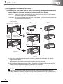
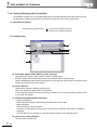
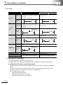
(1) Replacing the CPU module with the QCPU, and replacing existing modules with the Q
series modules in series with utilizing the existing A/AnS series module
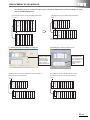
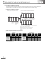
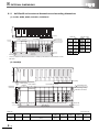
Method :
Replace the modules gradually by using the QA(1S) extension base unit (QA(1S)6
B)
and utilizing the property of AnS/QnAS series.
Advantage: The cost and workload for the transition can be divided, and yet the function extension can
be continued during the transition.
Existing modules
Main base unit
AnS series
Replacement
step 1
Q series
Replacement
step 2
Q series
AnS series
modules
Extension
base unit
(1st stage)
Extension
base unit
(1st stage)
Remount the
existing modules.
Q series
AnS series
modules
AnS series
modules
Remount the
existing modules.
Extension
base unit
(2nd stages)
QA1S extension
base unit
Q series
AnS series
modules
QA1S extension
base unit
(a) The QA(1S) extension base unit has the "QA6
B", supporting A series and "QA1S6
B",
supporting AnS series.
When replacing the A/QnA series, the AnS series module can be utilized.
(b) When utilizing existing A/AnS series module, programs can be utilized without changing the
existing I/O address with I/O assignment setting in PLC parameter.
For details of I/O address setting method with I/O assignment, refer to Section 5.4.6.
Point
The QA(1S) extension base unit can be used for the High Performance model QCPU (Q02CPU,
Q02HCPU, Q06HCPU, Q12HCPU, Q25HCPU) only. (Universal model QCPU to be supported soon.)
For details and precautions of the QA(1S) extension base unit, refer to Section 5.4.
1-4
1
INTRODUCTION
Replacement procedures:
Step 1
• Mount the QCPU and a module for function expansion on the Q series main base unit. Connect the
QA(1S) extension base unit (QA1S65B) to the main base unit as the first extension base unit and
mount the power supply module and I/O module which are installed to the existing AnS main base
unit series on it. (Wiring change is unnecessary.) If the first extension base unit is AnS series, replace
it with QA1S extension base unit (QA1S65B). If it is A series, replace it with QA extension base unit
(QA6B). Then mount a power supply module and I/O module on the extension base unit. (Wiring
change is unnecessary.)
• Programs are automatically converted* by changing the programmable controller type from AnS/
QnAS CPU to QCPU using GX Developer.
* Some instructions are not automatically converted. In case of intelligent function module or network module, programs and
parameters need be changed.
1-5
1
INTRODUCTION
Step 2
After replacing the existing modules mounted on the QA(1S) extension base unit with the Q series
modules, remove the QA extension base unit and QA(1S) series extension base unit.
Existing AnS module
Step 1
Functions can be added
Web server module.
QCPU for replacing the
existing AnSCPU
First extension base unit
Replace the existing AnS
main base unit with the
QA1S extension base unit
(QA1S68B). Then, mount
the modules mounted on
the existing main base unit
to the QA1S extension base
unit (utilization).
Second or later extension
bases unit
When the first extension
base unit is the AnS series,
replace with the QA1S
extension base unit.
When the first extension
base unit is the A series,
replace with the QA
extension base unit
(QA6 B).
1-6
Replace all the modules
with the Q series.
Q series
Use the QA1S extension
base unit.
(QA1S68B)
Step 2
Use the QA(1S) extension
base unit.
(QA(1S)68B)
Assets such as power supply modules and
I/O modules can be used.
+
Wiring change is unnecessary.
Q series
1
INTRODUCTION
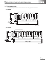
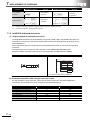
(2) Transition to Q series by utilizing existing wiring
Method :
Use the upgrade tool manufactured by Mitsubishi Electric Engineering Co., Ltd. and the
existing mounting hole/terminal block wiring.
Advantage: No need to process additional holes, and the existing wiring is usable.
AnS series I/O module
Q series I/O module
Base
adapter
Terminal block
*1
Conversion adapter
Remove the existing terminal block (with wiring)
and mount it.
*1
The terminal block cover (from the old terminal block) must be exchanged.
Remarks
(1)
Upgrade tool for transition from the AnS series to the Q series released from Mitsubishi Electric
Engineering Co., Ltd. is composed of the following products.
• Conversion adapter for changing the existing wiring connected to the AnS series I/O module to
wiring for the Q series I/O module
• Base adapter which utilizes the mounting hole of the AnS series base unit for mounting
MELSEC-Q series module
(2)
For example, using the conversion adapter allows utilizing the wiring connected to the AnS series
I/O module for the Q series module without change.
For details, refer to the catalog of the upgrade tool.
Using outside connection method, the existing wiring for AnS series input/output module
connector type is usable. (No need to change the wiring, only move the connecter to the Q series
module.)
Moreover, it is possible to mount a module used with the upgrade tool on the same base unit.
1-7
1
INTRODUCTION
Replacement procedures:
• Remove the existing AnS series modules together with the base unit, and use the existing mounting
holes to mount the upgrade tool (Base adapter) manufactured by Mitsubishi Electric Engineering Co.,
Ltd. Then mount the Q series. (By mounting the base adapter, it is not necessary to redo the mounting
holes.)
If the existing base unit is mounted on a DIN rail, the replaced Q series base unit can be directed
installed, so a base adaptor is unnecessary.
• Mount the upgrade tool (Conversion adapter) manufactured by Mitsubishi Electric Engineering Co.,
Ltd. on the mounted Q series I/O modules.
• Remove the terminal blocks wired from the existing AnS series I/O modules, and mount the blocks on
the conversion adapter. (The existing wiring is usable.)
• Programs are automatically converted* by changing the programmable controller type from AnS/
QnASCPU to QCPU using GX Developer. Even if the module arrangement is changed, the I/O can be
assigned to the same number as before, which cuts out the need to modify the programs and slot
number for I/O module.
* Some instructions are not automatically converted. In case of intelligent function module or network module, programs and
parameters need be changed.
Existing AnS series
Q series
Upgrade tool
(Base adapter)
1-8
1
INTRODUCTION
Point
(1)
Conversion adapter*1
Product
Input
MELSEC-AnS/QnAS Series
MELSEC-Q Series
module model
module model
QX10
QX40
A1SX40-S1
QX40-S1
A1SX80-S2
Output
Analog input
Analog output
(2)
ERNT-ASQTXY10
A1SX10, A1SX10EU
A1SX40, A1SX40-S2
A1SX80, A1SX80-S1,
Conversion adapter
ERNT-ASQTX40
QX80
ERNT-ASQTX80
A1SY10, A1SY10EU
QY10
ERNT-ASQTXY10
A1SY22
QY22
ERNT-ASQTY22
A1SY40, A1SY40P
QY40P
ERNT-ASQTY40
A1SY50
QY50
ERNT-ASQTY50
A1SY80
QY80
ERNT-ASQTY80
A1S64AD
Q64AD
ERNT-ASQT64AD
A1S68AD
Q68ADV
Q68ADI
A1S62DA
Q62DAN
A1S68DAV
Q68DAVN
A1S68DAI
Q68DAIN
ERNT-ASQT68AD
ERNT-ASQT62DA
ERNT-ASQT68DA
Base adapter*1
Product
MELSEC-AnS/QnAS Series
MELSEC-Q Series
module model
module model
Base adapter
A1S33B
Q33B
ERNT-ASQB33
A1S35B
Q35B
ERNT-ASQB35
A1S38B, A1S38HB
Q38B
ERNT-ASQB38
Extension base unit
A1S65B
Q65B
ERNT-ASQB65
(Power supply)
A1S68B
Q68B
ERNT-ASQB68
A1S55B
Q55B
ERNT-ASQB55
Main base unit
Extension base unit
(None power supply )
A1SJCPU
CPU module and base unit
A1SJCPU-S3
A1SJHCPU
*1
Q00JCPU
Q00UJCPU
ERNT-ASQB00J
When replacing a system using A series extension base unit that is connected to AnS/QnAS base unit, "Q large base unit,
Mitsubishi Electric Engineering Co.,Ltd. upgrate tool" can be used.
Please refer to the following for selection guidance.
Transition from MELSEC-A/QnA (Large Type) Series to Q Series Handbook (Fundamentals)
MELSEC-A/QnA Series Transition Examples
1-9
1
INTRODUCTION
For MELSEC-A/QnA(large type) Series to Q Series transition related products manufactured by Mitsubishi
Electric Engineering Co., Ltd. or Mitsubishi Electric System & Service Co., Ltd., contact your local sales office or
representative.
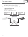
1.2.3 Precautions for transition
(1) Before replacing the A/AnS/QnA/QnAS series by the Q series, be sure to refer to manuals for
each Q series module to check the functions, specifications, and usage.
(2) For products manufactured by Mitsubishi Electric Engineering Co., Ltd. and Mitsubishi Electric
System & Service Co., Ltd., refer to the catalog for each product shown in Appendix to develop
an understanding of the detailed specifications, precautions and restrictions for use for correct
usage.
(3) After replacing the A/AnS/QnA/QnAS series by the Q series, be sure to check operations of
the whole system before the actual operation.
1 - 10
REPLACEMENT OF CPU MODULE
2
REPLACEMENT OF CPU MODULE
2
The following is an example of alternative Q series CPU modules that can be chosen based on
compatibility with previous AnS series CPU. The optimal AnS series replacement may be selected
based on type of control, specifications, system scalability and cost.
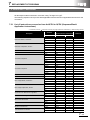
2.1 List of Alternative Models of CPU Module
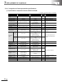
(1) Replacement with Universal model QCPU
AnS/QnAS series model
Product
Model
Q series alternative model
Model
Q00UJCPU
I/O control: Refresh/direct switch → Refresh only
Processing speed (LD instruction) : During refresh 0.33µs → 0.12µs
PC MIX value: 0.4 → 4.92
Number of I/O points: 256 points
Number of I/O device points: 2048 points → 8192 points
Program capacity: 8k steps → 10k steps
Number of file register points: 8k points → 0 points
Number of extension stages: 2 stages → 2 stages (GOT bus connection can be made up
to 2 stages.)
9) Applicable memory: Built-in RAM/E2PROM cassette (sold separately)
→ program memory/Standard ROM
10) Microcomputer program: available → not available
11) configuration: including 5 slot base unit, CPU module and power supply module
A1SJHCPU
CPU module
Remarks (restrictions)
1)
2)
3)
4)
5)
6)
7)
8)
Q00UCPU
1)
2)
3)
4)
5)
6)
7)
8)
I/O control: Refresh/direct switch → Refresh only
Processing speed (LD instruction) : During refresh 0.33µs → 0.08µs
PC MIX value: 0.4 → 7.36
Number of I/O points: 256 points → 1024 points
Number of I/O device points: 2048 points → 8192 points
Program capacity: 8k steps → 10k steps
Number of file register points: 8k points → 64k points
Number of extension stages: 1 stage → 4 stages (GOT bus connection can be made up to
4 stages.)
9) Applicable memory: Built-in RAM/E2PROM cassette (sold separately)
→ program memory/Standard RAM/Standard ROM
10) Microcomputer program: available → not available
A1SHCPU
Q00UCPU
1)
2)
3)
4)
5)
6)
7)
8)
I/O control: Refresh/direct switch → Refresh only
Processing speed (LD instruction) : During refresh 0.33µs → 0.08µs
PC MIX value: 0.4 → 7.36
Number of I/O points: 256 points → 1024 points
Number of I/O device points: 2048 points → 8192 points
Program capacity: 8k steps → 10k steps
Number of file register points: 8k points → 64k points
Number of extension stages: 1 stage → 4 stages (GOT bus connection can be made up to
4 stages.)
9) Applicable memory: Built-in RAM/E2PROM cassette (sold separately)
→ program memory/Standard RAM/Standard ROM
10) Microcomputer program: available → not available
2-1
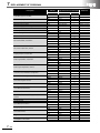
REPLACEMENT OF CPU MODULE
AnS/QnAS series model
Product
Model
A2SHCPU
Q series alternative model
Model
Q01UCPU
Remarks (restrictions)
1)
2)
3)
4)
5)
6)
7)
8)
I/O control: Refresh/direct switch → Refresh only
Processing speed (LD instruction) : During refresh 0.25µs → 0.06µs
PC MIX value: 0.5 → 9.79
Number of I/O points: 512 points → 1024 points
Number of I/O device points: 2048 points → 8192 points
Program capacity: 14k steps → 15k steps
Number of file register points: 8k points → 64k points
Number of extension stages: 1 stage → 4 stages (GOT bus connection can be made up to
4 stages.)
9) Applicable memory: Built-in RAM/E2PROM cassette (sold separately)
→ program memory/Standard RAM/Standard ROM
10) Microcomputer program: available → not available
A2USCPU
Q02UCPU
1)
2)
3)
4)
5)
6)
7)
I/O control: Refresh only
Processing speed (LD instruction) : 0.2µs → 0.04µs
PC MIX value: 0.9 → 14
Number of I/O points: 512 points → 2048 points
Number of I/O device points: 8192 points → 8192 points
Program capacity: 14k steps → 20k steps
Number of file register points: 8k points → 64k points (Using memory card: Max.4086k
points)
8) Number of extension stages: 1 stage → 4 stages (GOT bus connection can be made up to
4 stages.)
9) Applicable memory: Built-in RAM/E2PROM cassette (sold separately)
→ program memory/Standard RAM/Standard ROM/memory card (sold separately)
10) Microcomputer program: not available
11) Sequence instruction: AnA/AnU-dedicated instructions are replaceable.*1
CPU module
Q02UCPU
1)
2)
3)
4)
5)
6)
7)
I/O control: Refresh only
Processing speed (LD instruction) : 0.09µs → 0.04µs
PC MIX value: 2.0 → 14
Number of I/O points: 1024 points → 2048 points
Number of I/O device points: 8192 points → 8192 points
Program capacity: 30k steps → 20k steps
Number of file register points: 8k points → 64k points (Using memory card: Max.4086k
points)
8) Number of extension stages: 1 stage → 4 stages (GOT bus connection can be made up to
4 stages.)
9) Applicable memory: Built-in RAM/E2PROM cassette (sold separately)
→ program memory/Standard RAM/Standard ROM/memory card (sold separately)
10) Microcomputer program: not available
11) Sequence instruction: AnA/AnU-dedicated instructions are replaceable.*1
A2USHCPU-S1
Q03UDCPU
1)
2)
3)
4)
5)
6)
7)
I/O control: Refresh only
Processing speed (LD instruction) : 0.09µs → 0.02µs
PC MIX value: 2.0 → 28
Number of I/O points: 1024 points → 4096 points
Number of I/O device points: 8192 points → 8192 points
Program capacity: 30k steps → 30k steps
Number of file register points: 8k points → 96k points (Using memory card: Max.4086k
points)
8) Number of extension stages: 1 stage → 7 stages
9) Applicable memory: Built-in RAM/E2PROM cassette (sold separately)
→ program memory/Standard RAM/Standard ROM/memory card (sold separately)
10) Microcomputer program: not available
11) Sequence instruction: AnA/AnU-dedicated instructions are replaceable.*1
*1
2-2
The instruction for file registers and special function modules need to be replaced with those for the Q series.
REPLACEMENT OF CPU MODULE
AnS/QnAS series model
Product
Model
Q series alternative model
Model
Q02UCPU
Q2ASCPU
Q03UDCPU
CPU module
Q04UDHCPU
Q2ASCPU-S1
Q06UDHCPU
Remarks (restrictions)
1)
2)
3)
4)
5)
6)
7)
I/O control: Refresh only
Processing speed (LD instruction) : 0.2µs → 0.04µs
PC MIX value: 1.3 → 14
Number of I/O points: 512 points → 2048 points
Number of I/O device points: 8192 points → 8192 points
Program capacity: 28k steps → 20k steps
Number of file register points: 0k points (Memory card (sold separately) is necessary.)
→ 64k points (Using memory card: Max.4086k points)
8) Number of extension stages: 1 stage → 4 stages (GOT bus connection can be made up to
4 stages.)
9 Applicable memory: Built-in RAM/memory card (sold separately)
→ program memory/Standard RAM/Standard ROM/memory card (sold separately)
10) Microcomputer program: not available
1)
2)
3)
4)
5)
6)
7)
I/O control: Refresh only
Processing speed (LD instruction) : 0.2µs → 0.02µs
PC MIX value: 1.3 → 28
Number of I/O points: 512 points → 4096 points
Number of I/O device points: 8192 points → 8192 points
Program capacity: 14k steps → 30k steps
Number of file register points: 0k points (Memory card (sold separately) is necessary.)
→ 96k points (Using memory card: Max.4086k points)
8) Number of extension stages: 1 stage → 7 stages
9) Applicable memory: program memory/memory card (sold separately)
→ program memory/Standard RAM/Standard ROM/memory card (sold separately)
10) Microcomputer program: not available
1)
2)
3)
4)
5)
6)
7)
I/O control: Refresh only
Processing speed (LD instruction) : 0.2µs → 0.0095µs
PC MIX value: 1.3 → 60
Number of I/O points: 1024 points → 4096 points
Number of I/O device points: 8192 points → 8192 points
Program capacity: 60k steps → 40k steps
Number of file register points: 0k points (Memory card (sold separately) is necessary.)
→ 128k points (Using memory card: Max.4086k points)
8) Number of extension stages: 1 stage → 7 stages
9) Applicable memory: program memory/memory card (sold separately)
→ program memory/Standard RAM/Standard ROM/memory card (sold separately)
10) Microcomputer program: not available
1)
2)
3)
4)
5)
6)
7)
I/O control: Refresh only
Processing speed (LD instruction) : 0.2µs → 0.0095µs
PC MIX value: 1.3 → 60
Number of I/O points: 1024 points → 4096 points
Number of I/O device points: 8192 points → 8192 points
Program capacity: 60k steps → 60k steps
Number of file register points: 0k points (Memory card (sold separately) is necessary.)
→ 384k points (Using memory card: Max.4086k points)
8) Number of extension stages: 1 stage → 7 stages
9) Applicable memory: program memory/memory card (sold separately)
→ program memory/Standard RAM/Standard ROM/memory card (sold separately)
10) Microcomputer program: not available
2-3
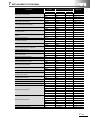
REPLACEMENT OF CPU MODULE
AnS/QnAS series model
Product
Model
Q series alternative model
Model
Q02UCPU
Q2ASHCPU
Q03UDCPU
CPU module
Q04UDHCPU
Q2ASHCPU-S1
Q06UDHCPU
2-4
Remarks (restrictions)
1)
2)
3)
4)
5)
6)
7)
I/O control: Refresh only
Processing speed (LD instruction) : 0.075µs → 0.04µs
PC MIX value: 3.8 → 14
Number of I/O points: 512 points → 2048 points
Number of I/O device points: 8192 points → 8192 points
Program capacity: 28k steps → 20k steps
Number of file register points: 0k points (Memory card (sold separately) is necessary.)
→ 64k points (Using memory card: Max.4086k points)
8) Number of extension stages: 1 stage → 4 stages (GOT bus connection can be made up to
4 stages.)
9) Applicable memory: program memory/memory card (sold separately)
→ program memory/Standard RAM/Standard ROM/memory card (sold separately)
10) Microcomputer program: not available
1)
2)
3)
4)
5)
6)
7)
I/O control: Refresh only
Processing speed (LD instruction) : 0.075µs → 0.02µs
PC MIX value: 3.8 → 28
Number of I/O points: 512 points → 4096 points
Number of I/O device points: 8192 points → 8192 points
Program capacity: 28k steps → 30k steps
Number of file register points: 0k points (Memory card (sold separately) is necessary.)
→ 96k points (Using memory card: Max.4086k points)
8) Number of extension stages: 1 stage → 7 stages
9) Applicable memory: program memory/memory card (sold separately)
→ program memory/Standard RAM/Standard ROM/memory card (sold separately)
10) Microcomputer program: not available
1)
2)
3)
4)
5)
6)
7)
I/O control: Refresh only
Processing speed (LD instruction) : 0.075µs → 0.0095µs
PC MIX value: 3.8 → 60
Number of I/O points: 1024 points → 4096 points
Number of I/O device points: 8192 points → 8192 points
Program capacity: 60k steps → 40k steps
Number of file register points: 0k points (Memory card (sold separately) is necessary.)
→ 128k points (Using memory card: Max.4086k points)
8) Number of extension stages: 1 stage → 7 stages
9) Applicable memory: program memory/memory card (sold separately)
→ program memory/Standard RAM/Standard ROM/memory card (sold separately)
10) Microcomputer program: not available
1)
2)
3)
4)
5)
6)
7)
I/O control: Refresh only
Processing speed (LD instruction) : 0.075µs → 0.0095µs
PC MIX value: 3.8 → 60
Number of I/O points: 1024 points → 4096 points
Number of I/O device points: 8192 points → 8192 points
Program capacity: 60k steps
Number of file register points: 0k points (Memory card (sold separately) is necessary.)
→ 384k points (Using memory card: Max.4086k points)
8) Number of extension stages: 1 stage → 7 stages
9) Applicable memory: program memory/memory card (sold separately)
→ program memory/Standard RAM/Standard ROM/memory card (sold separately)
10) Microcomputer program: not available
REPLACEMENT OF CPU MODULE
(2) Replacement with High Performance model QCPU
AnS/QnAS series model
Product
Model
Q series alternative model
Model
Q00JCPU
A1SJHCPU
Q00CPU
CPU module
A1SHCPU
A2SHCPU
A2USCPU
Q00CPU
Q01CPU
Q02CPU
Remarks (restrictions)
I/O control: refresh mode and direct mode switching → refresh only
Processing speed (LD instruction): at refresh 0.33µs → 0.2µs
PC MIX value: 0.4 → 1.6
Number of I/O points: 256 points → 256 points
Number of I/O device points: 2048 points → 2048 points
Program size: 8K steps → 8K steps
Number of file register points: 8K points → 0 points
Number of extension bases: 1 stage → 2 stages
Used memory: built-in RAM/EEP-ROM cassette (sold separately)
→ program memory/standard ROM
10) Microcomputer program: available → not available
11) Structure: 5-slot base unit, CPU module, and power supply module are integrated.
1)
2)
3)
4)
5)
6)
7)
8)
9)
I/O control: refresh mode and direct mode switching → refresh only
Processing speed (LD instruction): at refresh 0.33µs → 0.16µs
PC MIX value: 0.4 → 2.0
Number of I/O points: 256 points → 1024 points
Number of I/O device points: 2048 points → 2048 points
Program size: 8K steps → 8K steps
Number of file register points: 8K points → 64K points
Number of extension bases:1 stage → 4 stages
Used memory: built-in RAM/EEP-ROM cassette (sold separately)
→ program memory/standard RAM/standard ROM
10) Microcomputer program: available → not available
11) Structure: 5-slot base unit, CPU module, and power supply module are integrated.
→ Main base unit, CPU module, and power supply module are separated.
1)
2)
3)
4)
5)
6)
7)
8)
9)
I/O control: refresh mode and direct mode switching → refresh only
Processing speed (LD instruction): at refresh 0.33µs → 0.16µs
PC MIX value: 0.4 → 2.0
Number of I/O points: 256 points → 1024 points
Number of I/O device points: 2048 points → 2048 points
Program size: 8K steps → 8K steps
Number of file register points: 8K points → 64K points
Number of extension bases: 1 stage → 4 stages
Used memory: built-in RAM/EEP-ROM cassette (sold separately)
→ program memory/standard RAM//standard ROM
10) Microcomputer program: available → not available
1)
2)
3)
4)
5)
6)
7)
8)
9)
I/O control: refresh mode and direct mode switching → refresh only
Processing speed (LD instruction): at refresh 0.25µs → 0.1µs
PC MIX value: 0.5 → 2.7
Number of I/O points: 512 points → 1024 points
Number of I/O device points: 2048 points → 2048 points
Program size: 14K steps →14K steps
Number of file register points: 8K points → 64K points
Number of extension bases: 1 stage → 4 stages
Used memory: built-in RAM/EEP-ROM cassette (sold separately)
→ program memory/standard RAM//standard ROM
10) Microcomputer program: available → not available
1)
2)
3)
4)
5)
6)
7)
8)
9)
1)
2)
3)
4)
5)
6)
7)
I/O control: refresh only
Processing speed (LD instruction): 0.2µs → 0.079µs
PC MIX value: 0.9 → 4.4
Number of I/O points: 512 points → 4096 points
Number of I/O device points: 8192 points → 8192 points
Program size: 14K steps → 28K steps
Number of file register points: 8K points → 32K points (Using memory card: Max.1018k
points)
8) Number of extension bases: 1 stage → 7 stages
9) Used memory: built-in RAM/EEP-ROM cassette (sold separately)
→ program memory/standard RAM/standard ROM/memory card (sold separately)
10) Microcomputer program: not available
11) Sequence instruction: AnA/AnU-dedicated instructions are replaceable.*1
2-5
REPLACEMENT OF CPU MODULE
AnS/QnAS series model
Product
Model
Q series alternative model
Model
Remarks (restrictions)
Q02HCPU
1)
2)
3)
4)
5)
6)
7)
I/O control: refresh only
Processing speed (LD instruction): 0.09µs → 0.034µs
PC MIX value: 2.0 → 10.3
Number of I/O points: 1024 points → 4096 points
Number of I/O device points: 8192 points → 8192 points
Program size: 30K steps → 28K steps
Number of file register points: 8K points → 64K points (Using memory card: Max.1018k
points)
8) Number of extension bases: 1 stage → 7 stages
9) Used memory: built-in RAM/EEP-ROM cassette (sold separately)
→ program memory/standard RAM/standard ROM/memory card (sold separately)
10) Microcomputer program: not available
Q06HCPU
1)
2)
3)
4)
5)
6)
7)
11) Sequence instruction: AnA/AnU-dedicated instructions are replaceable.*1
A2USHCPU-S1
I/O control: refresh only
Processing speed (LD instruction): 0.09µs → 0.034µs
PC MIX value: 2.0 → 10.3
Number of I/O points: 1024 points → 4096 points
Number of I/O device points: 8192 points → 8192 points
Program size: 30K steps → 60K steps
Number of file register points: 8K points → 64K points (Using memory card: Max.1018k
points)
8) Number of extension bases: 1 stage → 7 stages
9) Used memory: built-in RAM/EEP-ROM cassette (sold separately)
→ program memory/standard RAM/standard ROM/memory card (sold separately)
10) Microcomputer program: not available
11) Sequence instruction: AnA/AnU-dedicated instructions are replaceable.*1
CPU module
Q2ASCPU
Q2ASCPU-S1
Q2ASHCPU
2-6
Q02HCPU
Q06HCPU
Q02HCPU
1)
2)
3)
4)
5)
6)
7)
I/O control: refresh only
Processing speed (LD instruction): 0.2µs → 0.034µs
PC MIX value: 1.3 → 10.3
Number of I/O points: 512 points → 4096 points
Number of I/O device points: 8192 points → 8192 points
Program size: 28K steps → 28K steps
Number of file register points: 0K points (A memory card (sold separately) is required for
use.) → 64K points (Using memory card: Max.1018k points)
8) Number of extension bases: 1 stage → 7 stages
9) Used memory: built-in RAM/memory card (sold separately)
→ program memory/standard RAM/standard ROM/memory card (sold separately)
10) Microcomputer program: not available
1)
2)
3)
4)
5)
6)
7)
I/O control: refresh only
Processing speed (LD instruction): 0.2µs → 0.034µs
PC MIX value: 1.3 → 10.3
Number of I/O points: 1024 points → 4096 points
Number of I/O device points: 8192 points → 8192 points
Program size: 60K steps → 60K steps
Number of file register points: 0K points (A memory card (sold separately) is required for
use.) → 64K points (Using memory card: Max.1018k points)
8) Number of extension bases: 1 stage → 7 stages
9) Used memory: built-in RAM/memory card (sold separately)
→ program memory/standard RAM/standard ROM/memory card (sold separately)
10) Microcomputer program: not available
1)
2)
3)
4)
5)
6)
7)
I/O control: refresh only
Processing speed (LD instruction): 0.075µs → 0.034µs
PC MIX value: 3.8 → 10.3
Number of I/O points: 512 points → 4096 points
Number of I/O device points: 8192 points → 8192 points
Program size: 28K steps → 28K steps
Number of file register points: 0K points (A memory card (sold separately) is required for
use.) → 64K points (Using memory card: Max.1018k points)
8) Number of extension bases: 1 stage → 7 stages
9) Used memory: built-in RAM/memory card (sold separately)
→ program memory/standard RAM/standard ROM/memory card (sold separately)
10) Microcomputer program: not available
REPLACEMENT OF CPU MODULE
AnS/QnAS series model
Product
CPU module
*1
Model
Q2ASHCPU-S1
Q series alternative model
Model
Q06HCPU
Remarks (restrictions)
1)
2)
3)
4)
5)
6)
7)
I/O control: refresh only
Processing speed (LD instruction): 0.075µs → 0.034µs
PC MIX value: 3.8 → 10.3
Number of I/O points: 1024 points → 4096 points
Number of I/O device points: 8192 points → 8192 points
Program size: 60K steps → 60K steps
Number of file register points: 0K points (A memory card (sold separately) is required for
use.) → 64K points (Using memory card: Max.1018k points)
8) Number of extension bases: 1 stage → 7 stages
9) Used memory: built-in RAM/memory card (sold separately)
→ program memory/standard RAM/standard ROM/memory card (sold separately)
10) Microcomputer program: not available
The instruction for file registers and special function modules need to be replaced with those for the Q series.
Point
The specification comparison between AnS/QnASCPU and Basic model QCPU is in the Appendices.
2-7
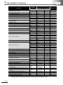
REPLACEMENT OF CPU MODULE
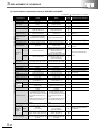
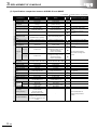
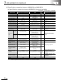
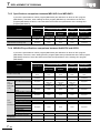
2.2 Comparison of CPU Module Specifications
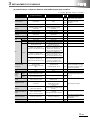
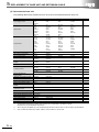
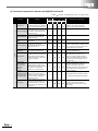
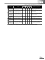
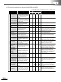
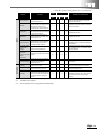
(1) Comparison between AnS/QnASCPU and Universal model QCPU
{: Available
: Although available, specifications such as setting method partially differ.
AnS series
Function
Description
×: Not available
QnAS series
A1SJHCPU
A1SHCPU
A2SHCPU
A2USCPU
A2USHCPU
-S1
Q2ASCPU
Q2ASCPU-S1
Q2ASHCPU
Q2ASHCPU-S1
{
{
{
{
{
{
{
{
{
{
{
{
*1
*1
*2
*2
*2
*2
Control method
Repetitive operation of
stored program
I/O control
method
Refresh mode/direct
mode
Programming
language
Language dedicated to
sequence control (relay
symbol, logic symbol,
MELSAP language)
{
{
{
{
{
{
Processing speed
Sequence instructions
(µs/steps)
0.33
0.25
0.2
0.09
0.2
0.075
Watchdog timer
(WDT)
Watchdog timer (WDT)
(ms)
10 to 2000
10 to 2000
200
200
10 to 2000
10 to 2000
64K
(RAM)
64K
(RAM)
64K
(RAM)
256K
(RAM)
Program
memory (RAM)
Program
memory (RAM)
*3
*3
*3
*3
*7
*7
Memory card
(Max. 2M)
Memory card
(Max. 2M)
User memory built-in
capacity (byte)
Memory capacity
Sold
separately
Sequence program
(steps)
Program capacity
Number of I/O
points
2-8
Microcomputer program
(byte)
Number of I/O points
(point)*6
Memory
Memory
Memory
Memory
cassette*4
(EEP-ROM)
cassette*4
(EEP-ROM)
cassette*4
(EEP-ROM)
cassette*4
(EEP-ROM)
Max. 8K
Max. 14K
Max. 14K
Max. 30K
Max. 28K
(-S1: 60K)
Max. 28K
(-S1: 60K)
Max. 14K*8
Max. 26K*8
×
×
×
×
256
512
512
1024
512
(-S1:1024)
512
(-S1:1024)
*1
I/O control mode (refresh mode or direct mode) is selectable with the I/O control method setting switch.
*2
Only refresh mode is available, but there are instructions and devices that can use direct mode.
*3
Free space areas (except that in the program memory) can be used as user memory.
*4
Memory cassette is for copying programs to the ROM. Use of the cassette does not increase the memory capacity.
*5
Only one memory card can be used.
*6
This number means the number of applicable points for the access to actual I/O modules.
*7
The memory capacity corresponds to the maximum number of steps in a sequence program.
*8
The program capacity is included to a sequence program.
REPLACEMENT OF CPU MODULE
{: Available
: Although available, specifications such as setting method partially differ.
×: Not available
Universal model QCPU
Q00UJCPU
Q00UCPU
Q01UCPU
Q02UCPU
Q03UDCPU
Q04UDHCPU
Q06UDHCPU
{
{
{
{
{
{
{
{
{
{
{
{
{
{
*2
*2
*2
*2
*2
*2
*2
{
{
{
{
{
{
{
0.12
0.08
0.06
0.04
0.02
0.0095
0.0095
10 to 2000
10 to 2000
10 to 2000
10 to 2000
10 to 2000
10 to 2000
10 to 2000
(Set in units of 10ms)
• Program
• Program
• Program
• Program
memory*7:
memory*7:
memory*7:
memory*7:
40K
40K
60K
80K
• Standard
• Standard
• Standard
• Standard
RAM: RAM: 128K
RAM: 128K
RAM: 128K
• Standard
• Standard
• Standard
• Standard
ROM: 256K
ROM: 512K
ROM: 512K
ROM: 512K
×
×
×
Max. 10K
Max. 10K
Max. 15K
• Program
• Program
• Program
memory*7:
120K
• Standard
RAM: 192K
• Standard
ROM:
1024K
memory*7:
160K
• Standard
RAM: 256K
• Standard
ROM:
1024K
memory*7:
240K
• Standard
RAM: 768K
• Standard
ROM:
1024K
Memory card
Memory card
Memory card
Memory card
*5
*5
*5
*5
RAM: Max. 8M
Flash: Max.
4M
ATA: Max. 32M
RAM: Max. 8M
Flash: Max.
4M
ATA: Max. 32M
RAM: Max. 8M
Flash: Max.
4M
ATA: Max. 32M
RAM: Max. 8M
Flash: Max.
4M
ATA: Max. 32M
Max. 20K
Max. 30K
Max. 40K
Max. 60K
×
×
×
×
×
×
×
256
1024
1024
2048
4096
4096
4096
Precautions for replacement
Reference
For the Q series, only refresh
mode is available. To input or
output data in direct mode, use the
direct input/output dedicated
instructions.
The MELSAP language for the A/
AnS series is MELSAP-ll and that
for the QnA/Q2AS/Q series is
MELSAP3.
-
-
-
-
For the Q series, microcomputer
programs cannot be used.
Consider replacing those
microcomputer programs with
sequence programs.
-
2-9
REPLACEMENT OF CPU MODULE
{: Available
: Although available, specifications such as setting method partially differ.
AnS series
Function
Description
QnA Sseries
A1SJHCPU
A1SHCPU
A2SHCPU
A2USCPU
Input device (X)*9
2048
2048
Output device (Y)*9
2048
2048
Internal relay (M)
×: Not available
A2USHCPU-S1
Q2ASCPU
Q2ASCPU-S1
Q2ASHCPU
Q2ASHCPU-S1
8192
8192
8192
8192
8192
8192
8192
8192
8192
8192
8192
8192
8192*10
8192*10
Total
2048
Total
2048
Total
8192
Total
8192
Annunciator (F)
256
256
2048
2048
2048
2048
Edge relay (V)
×
×
×
×
2048
2048
Link relay (B)
1024
1024
8192
8192
8192
8192
Timer (T)
256
256
2048 (default: 256)
2048
2048
Counter (C)
256
256
1024 (default: 256)
1024
1024
Data register (D)
1024
1024
8192
8192
12288
12288
Link register (W)
1024
1024
8192
8192
8192
8192
Latch relay (L)
steps relay (S)
(R)
File register
*11
32768*11
8192
8192
8192
8192
×
×
×
×
Max. 1018K
Max. 1018K
2
2
2
2
×
×
(Z)
1
1
7
7
16
16
(V)
1
1
7
7
×
×
(ZR)
32768
Number of device
points (point)
Accumulator (A)
Index register
Number of
comment points
Nesting (N)
8
8
8
8
15
15
Pointer (P)
256
256
256
256
4096
4096
Interrupt pointer (I)
32
32
32
32
48
48
Special relay (M/SM)
256
256
256
256
2048
2048
Special register (D/SD)
256
256
256
256
2048
2048
Special link relay (SB)
×
×
×
×
2048
2048
Special link register (SW)
×
×
×
×
2048
2048
Function input (FX)
×
×
×
×
16
16
Function output (FY)
×
×
×
×
16
16
Function register (FD)
×
×
×
×
5
5
Comment points
3648
3648
4032
4032
Extended comment
*13
Max. approx.50K Max. approx.50K
*11*12
*11*12
3968
3968
3968
3968
×
×
Self-diagnostics
Watchdog timer (WDT),
Memory error detection,
CPU error detection,
Battery error detection, etc.
{
{
{
{
{
{
Operation mode at
error occurrence
Stop/Continue setting
{
{
{
{
{
{
Output mode
switching at
changing from
STOP to RUN
Re-output operation status
before STOP/Selection of
output after operation
execution
{
{
{
{
{
{
2 - 10
*9
The points indicate the number of usable points in the program.
*10
For the QnAS and Q series, the steps relay (S) is dedicated for SFC programs.
*11
A memory card (sold separately) is required.
*12
The points apply when the size of a memory card used is 2M bytes.
*13
The number of comment points indicate the maximum number of points that can be written to the CPU module.
REPLACEMENT OF CPU MODULE
{: Available
: Although available, specifications such as setting method partially differ.
×: Not available
Universal model QCPU
Q00UCPU
Q01UCPU
Q02UCPU
Q03UDCPU
8192
8192
8192
8192
8192
8192
8192
-
8192
8192
8192
8192
8192
8192
8192
-
8192
8192
8192
8192
8192
8192
8192
-
8192
8192
8192
8192
8192
8192
8192
-
8192*10
8192*10
8192*10
8192*10
8192*10
8192*10
8192*10
-
2048
2048
2048
2048
2048
2048
2048
2048
2048
2048
2048
2048
2048
2048
-
8192
8192
8192
8192
8192
8192
8192
-
2048
2048
2048
2048
2048
2048
2048
-
1024
1024
1024
1024
1024
1024
1024
-
12288
12288
12288
12288
12288
12288
12288
-
8192
8192
8192
8192
8192
8192
8192
-
×
32768
32768
32768
32768
32768
32768
-
131072
(capacity of
memory card:
+Max.4086K)
393216
(capacity of
memory card:
+Max.4086K)
-
The QnAS/Q series CPU modules
do not use the accumulator since the
instruction format is different from
that for the AnS series.
Upon replacement, the accumulator
is converted into the special register
(SD718, SD719). Program
modification is not required.
×
65536
65536
65536
98304
(capacity of
(capacity of
memory card: memory card:
+Max.4086K) +Max.4086K)
Q04UDHCPU Q06UDHCPU
Precautions for replacement
Q00UJCPU
×
×
×
×
×
×
×
20
20
20
20
20
20
20
-
×
For the QnAS/Q series, this device is
used as the edge relay.
×
×
×
×
×
×
15
15
15
15
15
15
15
-
512
512
512
4096
4096
4096
4096
-
128
128
128
256
256
256
256
-
2048
2048
2048
2048
2048
2048
2048
-
2048
2048
2048
2048
2048
2048
2048
-
2048
2048
2048
2048
2048
2048
2048
-
2048
2048
2048
2048
2048
2048
2048
-
16
16
16
16
16
16
16
-
16
16
16
16
16
16
16
-
5
5
5
5
5
5
5
-
Within
program
memory+Stan
dard ROM
Within program memory
+Standard RAM
+Standard ROM
Reference
-
×
×
×
×
×
×
×
-
{
{
{
{
{
{
{
-
{
{
{
{
{
{
{
-
{
{
{
{
{
{
{
-
2 - 11
REPLACEMENT OF CPU MODULE
(2) Comparison between AnS/QnASCPU and High Performance model QCPU
AnS/series
Function
Description
A1SJHCPU
A1SHCPU
A2SHCPU
{
QnAS series
A2USCPU
A2USHCPU
-S1
Q2ASCPU
Q2ASCPU-S1
Q2ASHCPU
Q2ASHCPU-S1
{
{
{
{
{
{
{
{
{
{
{
*1
*1
*2
*2
*2
*2
Control method
Repetitive operation of
stored program
I/O control
method
Refresh mode/direct
mode
Programming
language
Language dedicated to
sequence control (relay
symbol, logic symbol,
MELSAP language)
{
{
{
{
{
{
Processing speed
Sequence instructions
(µs/steps)
0.33
0.25
0.2
0.09
0.2
0.075
Watchdog timer
(WDT)
Watchdog timer (WDT)
(ms)
10 to 2000
10 to 2000
200
200
10 to 2000
10 to 2000
64K
(RAM)
64K
(RAM)
64K
(RAM)
256K
(RAM)
Program
memory (RAM)
Program
memory (RAM)
*3
*3
*3
*3
*7
*7
Memory card
(Max. 2M)
Memory card
(Max. 2M)
User memory built-in
capacity (byte)
Memory capacity
Sold
separately
Sequence program
(steps)
Program capacity
Number of I/O
points
2 - 12
Microcomputer program
(byte)
Number of I/O points
(point)*6
Memory
Memory
Memory
Memory
cassette*4
(EEP-ROM)
cassette*4
(EEP-ROM)
cassette*4
(EEP-ROM)
cassette*4
(EEP-ROM)
Max. 8K
Max. 14K
Max. 14K
Max. 30K
Max. 28K
(-S1: 60K)
Max. 28K
(-S1: 60K)
Max. 14K*8
Max. 26K*8
×
×
×
×
256
512
512
1024
512
(-S1:1024)
512
(-S1:1024)
*1
I/O control mode (refresh mode or direct mode) is selectable with the I/O control method setting switch.
*2
Only refresh mode is available, but there are instructions and devices that can use direct mode.
*3
Free space areas (except that in the program memory) can be used as user memory.
*4
Memory cassette is for copying programs to the ROM. Use of the cassette does not increase the memory capacity.
*5
Only one memory card can be used.
*6
This number means the number of applicable points for the access to actual I/O modules.
*7
The memory capacity corresponds to the maximum number of steps in a sequence program.
*8
The program capacity is included to a sequence program.
REPLACEMENT OF CPU MODULE
{: Available
: Although available, specifications such as setting method partially differ.
Basic model QCPU
×: Not available
High Performance model QCPU
Q00JCPU
Q00CPU
Q01CPU
Q02CPU
Q02HCPU
Q06HCPU
{
{
{
{
{
{
{
{
{
{
{
{
*2
*2
*2
*2
*2
*2
Precautions for replacement Reference
-
-
For the Q series, only refresh
mode is available. To input or
output data in direct mode, use
the direct input/output
dedicated instructions.
-
-
{
{
{
{
{
{
The MELSAP language for the
A/AnS series is MELSAP-ll
and that for the QnA/Q2AS/Q
series is MELSAP3.
0.2
0.16
0.1
0.079
0.034
0.034
-
-
10 to 2000
10 to 2000
10 to 2000
10 to 2000
10 to 2000
10 to 2000
-
-
-
Section
2.4.1
• Program
memory
(RAM)*7 58K
• Standard
ROM*7: 58K
• Program
memory
• Program
memory
• Program
memory
• Program
memory
• Program
memory
(RAM)*7 94K
• Standard
(RAM)*7 94K
• Standard
(RAM)*7 112K
• Standard
(RAM)*7 112K
• Standard
(RAM)*7 240K
• Standard
ROM*7:
94K
• Standard RAM
128K
ROM*7:
ROM*7:
ROM*7:
ROM*7:
94K
• Standard RAM
128K
112K
• Standard RAM
64K
112K
• Standard RAM
128K
240K
• Standard RAM
128K
Memory card*5
RAM: Max. 2M
Flash: Max. 4M
ATA: Max. 32M
Memory card*5
RAM: Max. 2M
Flash: Max. 4M
ATA: Max. 32M
-
-
Max. 28K
Max. 60K
-
-
-
-
–
–
–
Memory card*5
RAM: Max. 2M
Flash : Max. 4M
ATA: Max. 32M
Max. 8K
Max. 8K
Max. 14K
Max. 28K
×
×
×
×
×
×
For the Q series,
microcomputer programs
cannot be used.
Consider replacing those
microcomputer programs with
sequence programs.
256
1024
1024
4096
4096
4096
-
2 - 13
REPLACEMENT OF CPU MODULE
{: Available
: Although available, specifications such as setting method partially differ.
AnS series
Function
Description
A1SJHCPU
A1SHCPU
A2SHCPU
Input device (X)*9
2048
Output device (Y)*9
2048
QnAS series
A2USCPU
A2USHCPU
-S1
Q2ASCPU
Q2ASCPU-S1
Q2ASHCPU
Q2ASHCPU-S1
2048
8192
8192
8192
8192
2048
8192
8192
8192
8192
8192
8192
Internal relay (M)
Latch relay (L)
Total 2048
×: Not available
Total 2048
Total 8192
Total 8192
steps relay (S)
8192
8192
8192*10
8192*10
2048
Annunciator (F)
256
256
2048
2048
2048
Edge relay (V)
×
×
×
×
2048
2048
Link relay (B)
1024
1024
8192
8192
8192
8192
Timer (T)
256
256
2048 (default: 256)
2048
2048
Counter (C)
256
256
1024 (default: 256)
1024
1024
Data register (D)
1024
1024
8192
8192
12288
12288
Link register (W)
1024
1024
8192
8192
8192
8192
8192
8192
8192
8192
32768*11
32768*11
×
×
×
Max. 120K
Max. 1018K
Max. 1018K
2
2
2
2
×
×
(Z)
1
1
7
7
16
16
(V)
1
1
7
7
×
×
(R)
File register
(ZR)
Number of device
points (point)
Accumulator (A)
Index register
Number of
comment
Nesting (N)
8
8
8
8
15
15
Pointer (P)
256
256
256
256
4096
4096
Interrupt pointer (I)
32
32
32
32
48
48
Special relay (M/SM)
256
256
256
256
2048
2048
Special register (D/SD)
256
256
256
256
2048
2048
Special link relay (SB)
×
×
×
×
2048
2048
Special link register (SW)
×
×
×
×
2048
2048
Function input (FX)
×
×
×
×
16
16
Function output (FY)
×
×
×
×
16
16
Function register (FD)
×
×
×
×
5
5
Max. approx.
50K
Max. approx.
50K
Comment points
3648
3648
3648
4032
*11 *12
*11 *12
Extended comment
×
×
×
3968
×
×
Self-diagnostics
Watchdog timer (WDT),
Memory error detection, CPU
error detection, Battery error
detection, etc.
{
{
{
{
{
{
Operation mode
at error
occurrence
Stop/Continue setting
{
{
{
{
{
{
Output mode
switching at
changing from
STOP to RUN
Re-output operation status
before STOP/Selection of
output after operation
execution
{
{
{
{
{
{
*13
points
2 - 14
*9
The points indicate the number of usable points in the program.
*10
For the QnAS and Q series, the steps relay (S) is dedicated for SFC programs.
*11
A memory card (sold separately) is required.
*12
The points apply when the size of a memory card used is 2M bytes.
*13
The number of comment points indicate the maximum number of points that can be written to the CPU module.
REPLACEMENT OF CPU MODULE
{: Available
Basic model QCPU
: Although available, specifications such as setting method partially differ.
×: Not available
High Performance model QCPU
Precautions for replacement
Reference
8192
-
-
8192
-
-
8192
8192
-
-
8192
8192
8192
-
-
2048*10
8192*10
8192*10
8192*10
-
-
1024
1024
2048
2048
2048
-
-
1024
1024
1024
2048
2048
2048
-
-
2048
2048
2048
8192
8192
8192
-
-
512
512
512
2048
2048
2048
-
-
512
512
512
1024
1024
1024
-
-
11136
11136
11136
12288
12288
12288
-
-
Q00JCPU
Q00CPU
Q01CPU
Q02CPU
Q02HCPU
Q06HCPU
2048
2048
2048
8192
8192
2048
2048
2048
8192
8192
8192
8192
8192
8192
2048
2048
2048
2048*10
2048*10
1024
2048
2048
2048
8192
8192
8192
-
-
×
32768
32768
32768
32768
32768
-
-
×
65536
65536
-
-
The QnAS/Q series CPU modules do
not use the accumulator since the
instruction format is different from that
for the AnS series.
Upon replacement, the accumulator is
converted into the special register
(SD718, SD719). Program
modification is not required.
-
32768
65536
65536
(capacity of
(capacity of
(capacity of
memory card: + memory card: + memory card: +
max. 1018K)
max. 1018K)
max. 1018K)
×
×
×
×
×
×
10
10
10
16
16
16
-
-
×
For the QnAS/Q series, this device is
used as the edge relay.
-
×
×
×
×
×
15
15
15
15
15
15
-
-
300
300
300
4096
4096
4096
-
-
128
128
128
256
256
256
-
-
1024
1024
1024
2048
2048
2048
-
-
1024
1024
1024
2048
2048
2048
-
-
1024
1024
1024
2048
2048
2048
-
-
1024
1024
1024
2048
2048
2048
-
-
16
16
16
16
16
16
-
-
16
16
16
16
16
16
-
-
5
5
5
5
5
5
-
-
Within standard
RAM capacity
Max. approx.
50K
Max. approx.
50K
Max. approx.
50K
-
-
Within the free
area size of the
program memory
Within standard
RAM capacity
×
×
×
×
×
×
-
-
{
{
{
{
{
{
-
-
{
{
{
{
{
{
-
-
{
{
{
{
{
{
-
-
2 - 15
REPLACEMENT OF CPU MODULE
2.3 Functional Comparison of CPU Module
2.3.1 Functional comparison between AnS series and Q series
(1) Comparison between QnASCPU and Universal model QCPU
{: Available
: Although available, specifications such as setting method partially differ.
AnS series
Control
Function
Description
Q series
Universal
Precautions for replacement
Reference
model*1
Constant scan
Executes the sequence program
at constant time intervals
regardless of the processing time
of the program.
{
{
Latch (data
retention during
power failure)
Holds the data of devices when
turning off the power, resetting,
and a momentary power failure
longer than the allowable
momentary power failure time
occurs.
{
{
{
-
-
Remote RUN/
STOP
Remotely runs or stops the
program operations in the CPU
module from external switches or
peripherals.
{
{
{
-
-
PAUSE
Stops operations while holding
the output status.
Interrupt
processing
Executes the program that
corresponds to the cause when
an interrupt cause occurs.
Microcomputer
mode
Executes various controls and
operations over utility programs
and user created microcomputer
programs stored in the
microcomputer program area by
calling them from the sequence
program.
{
Set this function with the special
register (D9020) for the AnS
series, and with parameters for
the Q series.
Set the PAUSE enable flag with
the special relay (M9040) for the
AnS/A2US series and with the
special relay (SM206) for the Q
{
-
-
series.*2
Display of priority of Sets the ERROR LED on/off
ERROR LED
status at an error.
ROM operation
2 - 16
A2USCPU
AnSHCPU A2USHCPU
-S1
×: Not available
Enables operation with
parameters and programs stored
in ROM not to lose user programs
due to battery exhaustion.
{
{
{
-
-
-
-
{
{
×
Consider use of sequence
program, etc., as the substitution.
Instructions from any utility
package need to be replaced with
the corresponding instructions of
the QCPU.
{
{
{
Target errors vary for each
module, but there is no functional
difference.
{
{
AnS series CPU modules can
perform the ROM operation by
using EEP-ROM cassette (sold
separately).
The Universal model QCPU,
whose program memory is a
Flash ROM, does not have to
perform the ROM operation.
*1
Universal model QCPU refers Q00UJCPU, Q00UCPU, Q01UCPU and others QnUCPUs.
*2
When PLC type in GX Developer changes, the number of device will change.
Section
7.7.12
REPLACEMENT OF CPU MODULE
{: Available
: Although available, specifications such as setting method partially differ.
AnS series
Function
Maintenance
Debug
Control
Data protection
function (system
protection, keyword
registration/
password
registration)
Description
Q series
High
A2USCPU
AnSHCPU A2USHCPU Performance
-S1
model*1
Prevents unauthorized access
from peripherals to programs
and comments in the built-in
memory of a CPU module,
memory cassettes, or memory
cards.
{
{
The settings for the output
status at changing from STOP
Output status
to RUN (Y) between "re-output
setting at changing
operation status before STOP"
from STOP to RUN
and "output after operation
execution".
{
{
×: Not available
{
Precautions for replacement
Reference
The Q series prohibits each file
from being read/written by
password registration, whereas
the AnS series prohibit the
parameters and programs from
being read/written to the user
memory by keyword registration.
Section
2.4.2
To replace the AnS series,
resetting the parameters is
necessary.
-
The Q series handles the year in
four digits (western calendar),
whereas the AnS series handles
the year in the last two digits.
-
For the Q series, it is necessary
to set the reserved capacity for
the write during RUN in advance.
Section
2.4.3
Clock function
Reads or writes the internal
clock data of the CPU module.
The clock data consists of year,
month, date, hour, minute,
second and a day of the week.
{
Write during RUN
Changes the programs of
(writes programs to) the
running CPU module.
{
{
{*3
Status latch
Stores the data of the entire
device memory area at the time
of error occurrence in the builtin memory or a memory
cassette and monitors the
stored data by a peripheral.
{
{
×
Sampling trace
Stores the data of the specified
device memory area in the
built-in memory or a memory
cassette at a set interval to
check the changes of the
device memory area and
monitors the stored data by a
peripheral.
{
{
{*4
-
-
steps operation
Stops the execution of a
sequence program at the
specified steps.
{
{
×
The Q series does not support
the steps operation function.
This function can be substituted
by the force external I/O ON/OFF
function.
-
Off-line switch
Separates the device memory
area used for the OUT
instruction from the operation
processing of sequence
program.
{
{
×
The Q series does not support
the off-line switch function.
-
Online I/O module
change
Replaces input/output modules
while the CPU module is in
operation.
×
×
×
To replace the input/output
modules online, use the Process
CPU.
-
Self-diagnostic
function
Performs self-diagnostics to
check for errors, detect errors,
and stop the CPU module.
{
{
{
Error codes differ between the
AnS series and Q series.
-
The Q series does not support
the status latch function.
*1
Universal model QCPU refers Q00UJCPU, Q00UCPU, Q01UCPU and others QnUCPUs.
*3
It is necessary to set the reserved capacity for the write during RUN in advance. (Default-set to 500 steps.)
*4
The function is not provided in Q00UJCPU.
-
2 - 17
REPLACEMENT OF CPU MODULE
(2) Comparison between AnSCPU and Basic model QCPU, High Performance model QCPU
{: Available
: Although available, specifications such as setting method partially differ.
AnS series
High
A2USCPU
Basic
Performance
AnSHCPU A2USHCPU
*1
model
-S1
model*2
Function
Description
Constant scan
Executes the sequence program at
constant time intervals regardless
of the processing time of the
program.
{
{
Latch (data
retention during
power failure)
Holds the data of devices when
turning off the power, resetting, and
a momentary power failure longer
than the allowable momentary
power failure time occurs.
{
{
{
Remote RUN/
STOP
Remotely runs or stops the
program operations in the CPU
module from external switches or
peripherals.
{
{
{
PAUSE
Stops operations while holding the
output status.
Interrupt
processing
Executes the program that
corresponds to the cause when an
interrupt cause occurs.
Microcomputer
mode
Executes various controls and
operations over utility programs
and user created microcomputer
programs stored in the
microcomputer program area by
calling them from the sequence
program.
{
×
×
Display of priority
of ERROR LED
Sets the ERROR LED on/off status
at an error.
{
{
{
{
×: Not available
Q series
Precautions for replacement
Reference
Set this function with the special
register (D9020) for the AnS
series, and with parameters for
the Q series.
-
{
-
-
{
-
-
Set the PAUSE enable flag with
the special relay (M9040) for the
AnS series, and with the special
{
-
Control
relay (SM206) for the Q series.*3
{
{
{
-
{
-
×
Consider use of sequence
program, etc., as the
substitution.
Instructions from any utility
package need to be replaced
with the corresponding
instructions of the QCPU.
-
{
Target errors vary for each
module, but there is no functional
difference.
-
For the AnS series CPU
ROM operation
2 - 18
Enables operation with parameters
and programs stored in ROM not to
lose user programs due to battery
exhaustion.
{
{
modules, an E2PROM cassette
(sold separately) is required for
copying data to the ROM for
ROM operation.
The High Performance model
QCPU modules have the boot
operation function, which reads
sequence programs stored in the
built-in standard ROM or
memory card to the program
memory to perform ROM
operation.
Section
2.4.1
Section
7.7.12
*1
The "Basic model" is a generic term of Q00JCPU, Q00CPU and Q01CPU.
*2
The "High Performance model" is the generic term of Q02CPU, Q02HCPU, Q06HCPU, Q12HCPU, and Q25HCPU.
*3
Device numbers are converted upon the programmable controller type change by GX Developer.
REPLACEMENT OF CPU MODULE
{: Available
: Although available, specifications such as setting method partially differ.
AnS series
Function
Description
Maintenance
Debug
Control
Data protection
function (system
protection, keyword
registration/
password
registration)
×: Not available
Q series
A2USCPU
Basic
AnSHCPU A2USHCPU
model*1
-S1
Prevents unauthorized access from
peripherals to programs and
comments in the built-in memory of
a CPU module, memory cassettes,
or memory cards.
{
{
The settings for the output status at
Output status
changing from STOP to RUN (Y)
setting at changing between "re-output operation
from STOP to RUN status before STOP" and "output
after operation execution".
{
{
High Performance
Precautions for replacement
Reference
The Q series prohibits each file
from being read/written by
password registration, whereas
the AnS series prohibit the
parameters and programs from
being read/written to the user
memory by keyword registration.
Section
2.4.2
*2
model
{
{
To replace the AnS series,
resetting the parameters is
necessary.
-
The Q series handles the year in
four digits (western calendar),
whereas the AnS series handles
the year in the last two digits.
-
Clock function
Reads or writes the internal clock
data of the CPU module.
The clock data consists of year,
month, date, hour, minute, second
and a day of the week.
{
{
Write during RUN
Changes the programs of (writes
programs to) the running CPU
module.
{
{
{*4
{*4
For the Q series, it is necessary to
set the reserved capacity for the
write during RUN in advance.
Section
2.4.3
Status latch
Stores the data of the entire device
memory area at the time of error
occurrence in the built-in memory
or a memory cassette and monitors
the stored data by a peripheral.
{
{
×
×
The Q series does not support the
status latch function.
-
Sampling trace
Stores the data of the specified
device memory area in the built-in
memory or a memory cassette at a
set interval to check the changes of
the device memory area and
monitors the stored data by a
peripheral.
{
{
×
{*5
-
-
steps operation
Stops the execution of a sequence
program at the specified steps.
{
{
×
×
The Q series does not support the
steps operation function.
Consider debugging with GX
Simulator.
-
Off-line switch
Separates the device memory area
used for the OUT instruction from
the operation processing of
sequence program.
{
{
×
×
The Q series does not support the
off-line switch function.
-
Online I/O module
change
Replaces input/output modules
while the CPU module is in
operation.
×
×
×
×
To replace the input/output
modules online, use the Process
CPU.
-
Self-diagnostic
function
Performs self-diagnostics to check
for errors, detect errors, and stop
the CPU module.
{
{
{
{
Error codes differ between the
AnS series and Q series.
-
*1
The "Basic model" is a generic term of Q00JCPU, Q00CPU and Q01CPU.
*2
The "High Performance model" is the generic term of Q02CPU, Q02HCPU, Q06HCPU, Q12HCPU, and Q25HCPU.
*4
It is necessary to set the reserved capacity for the write during RUN in advance. (Default-set to 500 steps.)
*5
The function is not provided in Q00JCPU.
2 - 19
REPLACEMENT OF CPU MODULE
2.3.2 Functional comparison between QnAS series and Q series
(1) Comparison between QnASCPU and Universal model QCPU
{: Available
: Although available, specifications such as setting method partially differ.
QnAS
series
Control
Function
Description
Q2ASCPU
(S1)
Q2ASHCPU
(S1)
×: Not available
Q series
Universal
Precautions for replacement
Reference
*1
model
Constant scan
Executes the sequence program at the
constant time intervals regardless of the
processing time of the program.
{
{
-
-
Latch (data
retention during
power failure)
Holds the data of devices when turning off
the power, resetting, and a momentary
power failure longer than the allowable
momentary power failure time occurs.
{
{
-
-
Remote RUN/
STOP
Remotely runs or stops the program
operations in the CPU module from external
switches or peripherals.
{
{
-
-
PAUSE
Stops operations while holding the output
status.
{
{
-
-
Interrupt
processing
Executes the program that corresponds to
the cause when an interrupt cause occurs.
{
{
-
-
Display priority of
ERROR LED
Sets the ERROR LED on/off status at an
error.
{
{
Target errors vary by model, but there is no
functional difference.
File management
Manages such as parameters, sequence
programs, device comments, file registers as
files.
{
{
Memory configuration and data to be stored
differ between the QnAS series and Q series.
{
{
Selects a suitable execution type for
Structured program program application, and divides each
program by designer, process or others.
I/O assignment
Assigns I/O points for each module
regardless of its mounted position.
Boot operation
(ROM operation)
Reads sequence programs stored in the
only or a memory card to the built-in memory
of the CPU module when the operating
status of the module is changed to RUN and
executes the read programs.
Data protection
function (system
protection,
keyword
registration/
password
registration)
Prevents unauthorized access from
peripherals to programs and comments in
the built-in memory of a CPU module or
memory cards.
-
-
When using a base unit with other than 8 slots,
set the number of slots with the parameter (I/O
assignment setting).
Section
2.4.4
{
The Universal model QCPU, whose program
memory is a Flash ROM, does not have to
perform the ROM operation.
Section
2.4.1
Section
7.7.12
{
The Q series prohibits each file from being read/
written by password registration, whereas the
QnAS series prohibit the parameters and
programs from being read/written to the user
memory by keyword registration.
Section
2.4.2
Section
2.4.1
{
{
Memory configuration and data to be stored
differ between the QnAS series and Q series.
Sets the output (Y) status at the change from
Output status
STOP to RUN to reoutputting data before
setting at changing
STOP or outputting data after the operation
from STOP to RUN
execution.
{
{
Resetting parameters is required to replace the
QnAS series with the Q series.
2 - 20
Section
2.4.1
{
Sets an initial value of device memory, file
registers, and special function modules
Initial device value
when the CPU module is set from STOP to
RUN.
*1
-
Universal model QCPU refers Q00UJCPU, Q00UCPU, Q01UCPU and others QnUCPUs.
-
REPLACEMENT OF CPU MODULE
{: Available
: Although available, specifications such as setting method partially differ.
QnA
series
Function
Description
Debug
Control
Number of general Sets the number of general data processing
data processing
executed in one END operation.
Q series
Precautions for replacement
Universal
model
Reference
*1
{
For the Q series, use the COM instructions or
set the communication reserved time with
special register (SD315) if necessary.
-
{
The Q series handles the year in four digits
(western calendar), whereas the QnAS series
handles the year in the last two digits.
Pay attention to the handling of the day of the
week data.
-
Clock function
Reads or writes the internal clock data of the
CPU module.
The clock data consists of year, month, day,
hour, minute, second and a day of the week.
Write during RUN
Changes the programs of (writes programs
to) the running CPU module.
{*2
{*2
For the Q series, it is necessary to set the
reserved capacity for the write during RUN in
advance.
Section
2.4.3
Status latch
Stores the data of the entire devices at the
time of error occurrence to the memory
cassette or built-in memory and monitors the
stored data by a peripheral.
{*3 *4
×
The Q series does not support the status latch
function.
-
Sampling trace
Stores the data of the specified device
memory area in a memory card at a set
interval to check the changes of the device
memory area and monitors the stored data
by a peripheral.
{*3
{*5
Program trace
Collects the execution status of the specified
steps in specified program and stores it in a
file.
{*3 *4
×
The Q series does not support the program
trace function.
-
{*3 *4
×
The Q series does not support the simulation
function.
Consider debugging with GX Simulator.
-
Detaches I/O modules or special modules
Simulation function from the CPU module and simulates the
program upon the steps operation.
Maintenance
Q2ASCPU
(S1)
Q2ASHCPU
(S1)
×: Not available
-
-
steps operation
Stops the execution of a sequence program
at the specified steps.
{
×
The Q series does not support the steps
operation function.
Consider debugging with GX Simulator.
-
Execution time
measurement
(program monitor
list, scan time
measurement)
Measures the processing time for each
program.
{
{
The execution time measurement can be
checked on the Program monitor list screen of
GX Developer.
-
Module access
interval read
Monitors the access interval of special
function modules or peripherals.
{
{
*6
-
Online I/O module
change
Replaces input/output modules while the
CPU module is in operation.
{
×
To replace the input/output modules online, use
the Process CPU.
-
Self-diagnostic
function
Performs self-diagnostics to check for errors,
detect errors, and stop the CPU module.
{
{
Error codes differ between the QnAS series and
Q series.
-
Error history
Stores errors that are detected with the
diagnostic function in the CPU module or
memory card.
The stored history data can be monitored
with a peripheral.
{
{
-
-
*1
Universal model QCPU refers Q00UJCPU, Q00UCPU, Q01UCPU and others QnUCPUs.
*2
It is necessary to set the reserved capacity for the write during RUN in advance. (Default-set to 500 steps.)
*3
A SRAM card is required.
*4
SW
IVD/NX-GPPQ is required.
*5
The function is not provided in Q00UJCPU.
*6
It is said "Module service interval time" in Q series.
2 - 21
REPLACEMENT OF CPU MODULE
(2) Comparison between QnASCPU and High Performance model QCPU
{: Available
: Although available, specifications such as setting method partially differ.
QnAS
series
Control
Function
Description
×: Not available
Q series
Q2ASCPU
High
(S1)
Performance
Q2ASHCPU
model*1
(S1)
Precautions for replacement
Reference
Constant scan
Executes the sequence program at the
constant time intervals regardless of the
processing time of the program.
{
{
-
-
Latch (data
retention during
power failure)
Holds the data of devices when turning off
the power, resetting, and a momentary
power failure longer than the allowable
momentary power failure time occurs.
{
{
-
-
Remote RUN/
STOP
Remotely runs or stops the program
operations in the CPU module from external
switches or peripherals.
{
{
-
-
PAUSE
Stops operations while holding the output
status.
{
{
-
-
Interrupt
processing
Executes the program that corresponds to
the cause when an interrupt cause occurs.
{
{
-
-
Display priority of
ERROR LED
Sets the ERROR LED on/off status at an
error.
{
{
Target errors vary by model, but there is no
functional difference.
File management
Manages such as parameters, sequence
programs, device comments, file registers as
files.
{
{
Memory configuration and data to be stored
differ between the QnAS series and Q series.
Section
2.4.1
{
{
-
-
{
When using a base unit with other than 8 slots,
set the number of slots with the parameter (I/O
assignment setting).
Section
2.4.4
{
The High Performance model QCPU modules
have the boot operation function, which reads
sequence programs stored in the built-in
standard ROM or memory card to the program
memory to perform ROM operation.
Section
2.4.1
Section
7.7.12
{
The Q series prohibits each file from being
read/written by password registration,
whereas the QnAS series prohibit the
parameters and programs from being read/
written to the user memory by keyword
registration.
Section
2.4.2
Section
2.4.1
Selects a suitable execution type for
Structured program program application, and divides each
program by designer, process or others.
I/O assignment
Assigns I/O points for each module
regardless of its mounted position.
Boot operation
(ROM operation)
Reads sequence programs stored in the
only or a memory card to the built-in memory
of the CPU module when the operating
status of the module is changed to RUN and
executes the read programs.
Data protection
function (system
protection,
keyword
registration/
password
registration)
Prevents unauthorized access from
peripherals to programs and comments in
the built-in memory of a CPU module or
memory cards.
Sets an initial value of device memory, file
registers, and special function modules
Initial device value
when the CPU module is set from STOP to
RUN.
{
{
Memory configuration and data to be stored
differ between the QnAS series and Q series.
Sets the output (Y) status at the change from
Output status
STOP to RUN to reoutputting data before
setting at changing
STOP or outputting data after the operation
from STOP to RUN
execution.
{
{
Resetting parameters is required to replace
the QnAS series with the Q series.
*1
2 - 22
-
The "High Performance model" is the generic term of Q02CPU, Q02HCPU, Q06HCPU, Q12HCPU, and Q25HCPU.
-
REPLACEMENT OF CPU MODULE
{: Available
: Although available, specifications such as setting method partially differ.
QnA
series
Function
Description
Maintenance
Debug
Control
Number of general Sets the number of general data processing
data processing
executed in one END operation.
×: Not available
Q series
Q2ASCPU
High
(S1)
Performance
Q2ASHCPU
model*1
(S1)
Precautions for replacement
Reference
{
For the Q series, use the COM instructions or
set the communication reserved time with
special register (SD315) if necessary.
-
{
The Q series handles the year in four digits
(western calendar), whereas the QnAS series
handles the year in the last two digits.
Pay attention to the handling of the day of the
week data.
-
Clock function
Reads or writes the internal clock data of the
CPU module.
The clock data consists of year, month, day,
hour, minute, second and a day of the week.
Write during RUN
Changes the programs of (writes programs
to) the running CPU module.
{*2
{*2
For the Q series, it is necessary to set the
reserved capacity for the write during RUN in
advance.
Section
2.4.3
Status latch
Stores the data of the entire devices at the
time of error occurrence to the memory
cassette or a memory card and monitors the
stored data by a peripheral.
{*3 *4
×
The Q series does not support the status latch
function.
-
Sampling trace
Stores the data of the specified device
memory area in a memory card at a set
interval to check the changes of the device
memory area and monitors the stored data
by a peripheral.
{*3
{*5
-
-
Program trace
Collects the execution status of the specified
steps in specified program and stores it in a
file.
{*3 *4
×
The Q series does not support the program
trace function.
-
Simulation
function
Detaches I/O modules or special modules
from the CPU module and simulates the
program upon the steps operation.
{*3 *4
×
The Q series does not support the simulation
function.
Consider debugging with GX Simulator.
-
steps operation
Stops the execution of a sequence program
at the specified steps.
{
×
The Q series does not support the steps
operation function.
Consider debugging with GX Simulator.
-
Execution time
measurement
(program monitor
list, scan time
measurement)
Measures the processing time for each
program.
{
{
The execution time measurement can be
checked on the Program monitor list screen of
GX Developer.
-
Module access
interval read
Monitors the access interval of special
function modules or peripherals.
{
{
*6
-
Online I/O module Replaces input/output modules while the
change
CPU module is in operation.
{
×
To replace the input/output modules online,
use the Process CPU.
-
Self-diagnostic
function
Performs self-diagnostics to check for errors,
detect errors, and stop the CPU module.
{
{
Error codes differ between the QnAS series
and Q series.
-
Error history
Stores errors that are detected with the
diagnostic function in the CPU module or
memory card.
The stored history data can be monitored
with a peripheral.
{
{
-
-
*1
The "High Performance model" is the generic term of Q02CPU, Q02HCPU, Q06HCPU, Q12HCPU, and Q25HCPU.
*2
It is necessary to set the reserved capacity for the write during RUN in advance. (Default-set to 500 steps.)
*3
A SRAM card is required.
*4
SW
IVD/NX-GPPQ is required. This is not applicable to GX Developer.
*5
The function is not provided in Q00JCPU.
*6
It is said "Module service interval time" in Q series.
2 - 23
REPLACEMENT OF CPU MODULE
2.4 Precautions for CPU Module Replacement
2.4.1 Memory for CPU module
The memory configuration is shown in (1). Examine the following points depending on the memory
capacity before replacement and applications.
• Memory to store
• To use or not to use a memory card
(1) Memory configuration and data that can be stored
(a) Universal model QCPU
Q series
AnS series
Built-in
memory
(RAM)
Program,
parameter,
comment,
file register
Program
memory
(Flash
ROM)
QnAS series
Program,
parameter,
comment,
initial device value
(Drive 0)
Memory
cassette
(EEP-ROM)
Program,
parameter
Standard
RAM
Program
memory
(RAM)
Program,
parameter,
comment,
initial device value
(Drive 0)
File register,
local device,
sampling trace
(Drive 3)
Standard
ROM
Program,
parameter,
comment,
initial device value
(Drive 4)
*1 Only one drive, drive 1 or drive 2,
can be used.
*2 The Q00UJCPU,Q00UCPU and
Q01UCPU do not have a memory
card slot.
Memory card
(RAM)
*1 *2
Program, parameter,
comment, initial device value,
file register, local device,
error history
(Drive 1)
Memory card
(ROM)
*1 *2
(Drive 1)
Program, parameter, comment,
initial device value,
file register
(Drive 2)
Memory
card A
(ROM)
(Drive 2)
Memory card (ROM)
can be replaced with a
memory card (ROM) to
perform ROM operation.
2 - 24
Memory
card A
(RAM)
Program, parameter,
comment,
initial device value,
file register,
local device,
error history
Program, parameter,
comment,
initial device value,
file register
REPLACEMENT OF CPU MODULE
(b) High Performance model QCPU
Q series
AnS series
Built-in
memory
(RAM)
Program,
parameter,
comment,
file register
Program
memory
(RAM)
QnAS series
Program,
parameter,
comment,
initial device value
(Drive 0)
Memory
cassette
(EEP-ROM)
Program,
parameter
Standard
RAM
*1 *2
Program
memory
(RAM)
Program,
parameter,
comment,
initial device value
(Drive 0)
File register,
local device,
sampling trace
(Drive 3)
Standard ROM can be
replaced to perform ROM
operation.
*1 The Q00JCPU does not have the
standard RAM.
*2 There are files that cannot be used
in the Basic model QCPU.
*3 Only one drive, drive 1 or drive 2,
can be used.
*4 The Basic model QCPU, Q00U(J)CPU,
Q01UCPU do not have a memory card.
Standard
ROM
Program,
parameter,
comment,
initial device value
(Drive 4)
Memory card
(RAM)
*3 *4
Program, parameter,
comment, initial device value,
file register, local device,
error history
(Drive 1)
Memory
card A
(RAM)
(Drive 1)
Program, parameter, comment,
Memory card
(ROM) *3 *4 initial device value,
file register
(Drive 2)
Memory
card A
(ROM)
Program, parameter,
comment,
initial device value,
file register,
local device,
error history
Program, parameter,
comment,
initial device value,
file register
(Drive 2)
Memory card (ROM)
can be replaced with the
standard ROM or a memory
card (ROM) to perform
ROM operation.
2 - 25
REPLACEMENT OF CPU MODULE
(2) Capacity of each memory
The following table shows the memory of CPU modules, in which the user program, etc. is stored,
together with its capacity.
(The memory capacity of each item is different according to CPU type. Please refer to the manual of
corresponding CPU.)
Model
Item
QnAS series
Max. 64K bytes
Max. 240K bytes
Max. 4000K bytes
Max. 1008K bytes
(A2USHCPU-S1: 256K bytes)
(program memory)
(program memory)
(program memory)
-
-
-
-
Max. 2M bytes
Max. 8M bytes
Max. 2M bytes
-
Max. 512k bytes
Flash card
-
Max. 1M byte
Max. 4M bytes
ATA card
-
-
Max. 32M bytes
Standard RAM
-
-
Standard ROM
-
-
Built-in RAM
Memory
cassette
E2PROM
SRAM card
Memory
card
2 - 26
Q series
AnS series
2
E PROM
card
32K bytes
(for writing programs to ROM)
High performance
Universal model
model
-
Max. 1792K bytes
Max. 256K bytes
(Q00UJCPU: none)
(Q00JCPU: none)
Max. 16384K bytes
Max. 1008K bytes
REPLACEMENT OF CPU MODULE
2.4.2 Keyword registration and password registration
The Q series prohibits reading from/writing to programs, etc. when a password is registered, as do the
AnS/QnAS series with keyword registration. Available functions are described below.
Item
Model
AnS series
QnAS series
Q series
Batch password setting for all files
Either of the following
provides the equivalent function.
The following attribute can
attributes can be set to the (Supplement)
Prohibition method for writing
be set to the specified
specified memory (drive).
to program, etc.
memory.
• Prohibition of read/write
By using a password, the following
• Prohibition of read/write/ attributes can be set to each specified
display
• Prohibition of write
file of the specified memory (drive).
• Prohibition of read/write/display
• Prohibition of write
2.4.3 Write during RUN
To execute the write during RUN, it is necessary to reserve the program size for increase upon the write
during RUN in advance.
(1) AnS series
The program size is decided by the parameter (memory capacity setting), and can be increased within
the capacity range upon write during RUN.
(2) QnAS/Q series
It is necessary to set the program size for increase upon the write during RUN in the Write to PLC
screen. (This set capacity is called as the write during RUN reserved steps. By default, 500 steps are
reserved.)
The following shows the setting screen for Allocate memory for Write during RUN as a reference.
2 - 27
REPLACEMENT OF CPU MODULE
2.4.4 Number of slots on the base unit
The following table shows how to determine the number of slots on the base unit for each series.
Item
Model
AnS series
QnAS series
Q series
Same as the actual number of slots. (The
number of slots can be determined in the
parameter setting.)
Number of slots on the
base unit
(Supplement)
Fixed to 8 slots regardless of the actual number.
If other than 8-slot base unit is used in the
Q series after replacement, set the start XY
address of each slot or set the number of
slots to "8" in the I/O assignment tab of the
PLC parameter dialog box.
2 - 28
REPLACEMENT OF CPU MODULE
The following gives an example of replacing the A1S35B+A1S68B system (default parameter is used)
with the Q35B+Q68B system.
(I/O assignment for the AnS series before replacement)
A1S35B
(I/O assignment for the Q series after replacement)
Q35B
2
3
4
X/Y0
X/Y10
X/Y20
X/Y30
X/Y40
16 points
16 points
16 points
16 points
16 points
5
6
7
8
9
10
11
12
X/Y50
13
1
X/Y80
After replacement, the start I/O numbers of
the first extension base unit will be "X/Y50".
16 points
Power supply module
16 points
Power supply
module
12
9
0
Q68B
A1S68B
8
CPU module
16 points
11
Power supply
module
16 points
10
16 points
15
16 points
14
16 points
7
Empty
3
16 points
6
16 points
X/Y20
16 points
5
Empty
2
X/Y10
X/Y0
CPU module
Power supply module
4
Empty
1
X/Y40
X/Y30
0
(1) Setting the start XY address of each slot
(2) Setting the number of slots to "8"
Setting the start XY
address of each slot
allows the CPU
module to use the
same XY address
used in the AnS
series CPU module.
(I/O assignment for the Q series when the start XY address of
each slot is set after replacement)
Setting the number
of slots allows the
CPU module to start
the I/O numbers of
the first extension
base unit from
X/Y80.
(I/O assignment for the Q series when the number
of slots of the base unit is set after replacement)
Q35B
Q35B
6
7
Empty
Empty
5
Empty
16 points
16 points
16 points
16 points
16 points
9
4
X/Y40
16 points
16 points
8
3
X/Y30
16 points
16 points
X/Y40
16 points
8
X/Y20
X/Y30
16 points
7
2
16 points
X/Y20
6
1
X/Y10
X/Y10
5
0
X/Y0
4
CPU module
3
Power supply
module
2
16 points
1
X/Y0
CPU module
Power supply
module
0
12
13
14
Q68B
Q68B
9
10
11
12
10
11
15
X/Y80
16 points
16 points
Power supply
module
X/Y80
Power supply
module
2 - 29
REPLACEMENT OF CPU MODULE
2.4.5 Base unit compatible with QCPU
The following table shows the base unit compatible with each QCPU type when replacing A/AnS/QnA/
QnAS series with Q series.
Base unit
Function
Universal model QCPU
High Performance model
QCPU
Main base unit
*1
Extension base unit
Q3B
Q3SB
Q00UJCPU*4
-
-
{
Q00UCPU
{
{
{
Q01UCPU
{
{
{
Q02UCPU
{
{
{
Q03UDCPU
{
{
{
Q04UDHCPU
{
{
{
Q06UDHCPU
{
{
{
Q02(H)CPU
{
{
{
Q06HCPU
{
{
{
Q12HCPU
{
{
{
*4
Basic model QCPU
Slim type main base unit
Q6B
Q00JCPU
-
-
{
Q00CPU
{
{
{
{
{
{
{
×
{
Q01CPU
Process CPU
Redundant CPU (Q series)
*5
-
-
-
MELSECNET/10
QJ72LP25-25
{
{
{
remote I/O station
QJ72BR15
{
{
{
*1
The extension base unit can not be connected.
*2
Q large type main base unit can not be used in a multiple CPU system.
*3
QA1S6B can not be used together with QA6ADP.
*4
The CPU module includes power supply module and base unit.
*5
A base unit for a redundant system is required.
*6
Universal model QCPUs can not be used with the QA(1S) extension base unit. (Planned to support in the future.)
Using QA(1S) extension base unit, version of Universal model QCPU is restricted.
(The QA(1S) extension base unit cannot be used by the existing Universal model QCPU.)
2 - 30
REPLACEMENT OF CPU MODULE
{ : Available
Q large base unit
: Not available (Planned to support in the future.) × : Not available
QA(1S)extension base unit
QA conversion adapter
A (large type) base
Q large main base unit
Q large extension base
*2
unit
Q3BL
Q6BL
-
×
*6
*6
×
{
{
*6
*6
×
{
{
*6
*6
×
{
{
*6
*6
×
{
{
*6
*6
×
{
{
*6
*6
×
{
{
*6
*6
×
{
{
{
{
{
{
{
{
{
{
{
{
{
{
{
QA extension base unit
QA6B
QA1S extension base
unit
QA1S6B
unit+QA conversion
adapter*3
QA6ADP
-
×
×
×
×
×
×
×
×
×
×
×
×
×
×
×
×
×
×
×
-
-
-
-
-
{
{
×
×
×
{
{
×
×
×
2 - 31
REPLACEMENT OF CPU MODULE
2.4.6 Programming tool and connection cable for Q series CPU
(1) Programming tool for Q series CPU
At the transition from MELSEC AnS/QnAS series to Q series, programming (including a programmable
controller type change for utilizing programs) for Q series CPUs is performed using GX Developer.
In this handbook, GX Developer is used as a programming tool.
Software packages other than GX Developer cannot be used.
(2) Connection cable for Q series CPU
When connecting a personal computer in which GX Developer has been installed to the Q series
CPU, RS-232 connection and USB connection are available.
The availability depending on CPU model is shown in the following table.
Note that the RS232/RS422 conversion cable for the AnS/QnAS series CPU are not applicable.
(a) Universal model QCPU
CPU model
RS-232 connection
USB connection
Q00UJCPU
Q00UCPU
Q01UCPU
Available
Available*1
Q02UCPU
(USB A type-USB miniB type)
Q03UDCPU
Q04UDHCPU
Q06UDHCPU
*1
Applicable cable is the QC30R2.
(b) Basic model QCPU, High Performance model QCPU
CPU model
RS-232 connection
USB connection
Q00JCPU
Q00CPU
Unavailable
Q01CPU
Q02CPU
Q02HCPU
Q06HCPU
Available*1
Q12HCPU
Available
Q12PHCPU
(USB A type-USB miniB type)
Q25HCPU
Q25PHCPU
*1
Applicable cable is the QC30R2.
Refer to GX Developer Operating Manual for details.
2 - 32
3
REPLACEMENT OF I/O MODULE
3
REPLACEMENT OF I/O MODULE
3
3.1 List of Alternative Models of I/O Module
AnS/QnAS series model
Product
Q series alternative model
Model
A1SX10
A1SX10EU
Model
QX10
QX10
1) External wiring: changed
2) Number of slots: not changed
3) Program
Number of occupied I/O points: not changed
4) Specifications
Rated input voltage: not changed
Rated input current: changed
On voltage/on current: not changed
Off voltage/off current: changed
Input resistance: changed
5) Function: not changed
QX28
1) External wiring: changed
2) Number of slots: changed (2 modules are required.)
3) Program
Number of occupied I/O points: changed (16 points → 32 points (16 points × 2
modules))
4) Specifications
Rated input voltage: not changed
Rated input current: changed
On voltage/on current: changed
Off voltage/off current: changed
Input resistance: changed
5) Function: not changed
Input module
A1SX20
A1SX20EU
Remarks (restrictions)
1) External wiring: changed
2) Number of slots: not changed
3) Program
Number of occupied I/O points: not changed
4) Specifications
Rated input voltage: not changed
Rated input current: changed
On voltage/on current: not changed
Off voltage/off current: changed
Input resistance: changed
5) Function: not changed
3-1
3
REPLACEMENT OF I/O MODULE
AnS/QnAS series model
Product
Q series alternative model
Model
A1SX30
Model
QX40
QX40
(24VDC)
1) External wiring: changed
2) Number of slots: not changed
3) Program
Number of occupied I/O points: not changed
4) Specifications
Rated input voltage: changed (12VDC is not applicable.)
Rated input current: changed
On voltage/on current: changed
Off voltage/off current: changed
Input resistance: changed
5) Function: not changed
QX70
(12VDC)
1) External wiring: changed
2) Number of slots: not changed
3) Program
Number of occupied I/O points: not changed
4) Specifications
Rated input voltage: changed (24VDC is not applicable.)
Rated input current: changed
On voltage/on current: changed
Off voltage/off current: changed
Input resistance: not changed
5) Function: not changed
QX40-S1
1) External wiring: changed
2) Number of slots: not changed
3) Program
Number of occupied I/O points: not changed
4) Specifications
Rated input voltage: not changed
Rated input current: changed
On voltage/on current: changed
Off voltage/off current: changed
Input resistance: changed
5) Function: not changed
QX40
1) External wiring: changed
2) Number of slots: not changed
3) Program
Number of occupied I/O points: not changed
4) Specifications
Rated input voltage: not changed
Rated input current: changed
On voltage/on current: changed
Off voltage/off current: changed
Input resistance: changed
5) Function: not changed
A1SX40
Input module
A1SX40-S1
A1SX40-S2
3-2
Remarks (restrictions)
Consider substituting the QX40 for it.
[When applying DC input]
1) External wiring: changed
2) Number of slots: not changed
3) Program
Number of occupied I/O points: not changed
4) Specifications
Rated input voltage: changed
(12VDC and AC input are not applicable.)*
Rated input current: changed
On voltage/on current: changed
Off voltage/off current: changed
Input resistance: changed
5) Function: not changed
*When 12VDC is required, use the QX70.
[When applying AC input]
Convert 24VAC to DC externally before input to the QX40.
3
REPLACEMENT OF I/O MODULE
AnS/QnAS series model
Product
Q series alternative model
Model
A1SX41
Model
QX41
(24VDC)
QX41-S2
(24VDC)
1) External wiring: not changed
2) Number of slots: not changed
3) Program
Number of occupied I/O points: not changed
4) Specifications
Rated input voltage: changed (12VDC is not applicable.)
Rated input current: changed (Approx.7mA → Approx.6mA)
On voltage/on current: changed
Off voltage/off current: changed
Input resistance: changed
5) Function: not changed
QX71
(12VDC)
1) External wiring: not changed
2) Number of slots: not changed
3) Program
Number of occupied I/O points: not changed
4) Specifications
Rated input voltage: changed (24VDC is not applicable.)
Rated input current: changed
On voltage/on current: changed
Off voltage/off current: changed
Input resistance: changed
5) Function: not changed
QX41-S1
1) External wiring: not changed
2) Number of slots: not changed
3) Program
Number of occupied I/O points: not changed
4) Specifications
Rated input voltage: not changed
Rated input current: changed
On voltage/on current: changed
Off voltage/off current: changed
Input resistance: changed
5) Function: not changed
QX41
1) External wiring: not changed
2) Number of slots: not changed
3) Program
Number of occupied I/O points: not changed
4) Specifications
Rated input voltage: not changed
Rated input current: changed (Approx.7mA → Approx.4mA)
On voltage/on current: changed
Off voltage/off current: changed
Input resistance: changed
5) Function: not changed
QX41-S2
1) External wiring: not changed
2) Number of slots: not changed
3) Program
Number of occupied I/O points: not changed
4) Specifications
Rated input voltage: not changed
Rated input current: changed (Approx.7mA → Approx.6mA)
On voltage/on current: changed
Off voltage/off current: changed
Input resistance: changed
5) Function: not changed
Input module
A1SX41-S1
Remarks (restrictions)
1) External wiring: not changed
2) Number of slots: not changed
3) Program
Number of occupied I/O points: not changed
4) Specifications
Rated input voltage: changed (12VDC is not applicable.)
Rated input current: changed (Approx.7mA → Approx.4mA)
On voltage/on current: changed
Off voltage/off current: changed
Input resistance: changed
5) Function: not changed
A1SX41-S2
3-3
3
REPLACEMENT OF I/O MODULE
AnS/QnAS series model
Product
Q series alternative model
Model
A1SX42
Model
QX42
(24VDC)
QX41-S2
(24VDC)
1) External wiring: not changed
2) Number of slots: changed (2 modules are required.)
3) Program
Number of occupied I/O points: not changed
(64 points =32 points × 2 modules)
4) Specifications
Rated input voltage: changed (12VDC is not applicable.)
Rated input current: changed (Approx.5mA → Approx.6mA)
On voltage/on current: changed
Off voltage/off current: changed
Input resistance: changed
5) Function: not changed
QX72
(12VDC)
1) External wiring: not changed
2) Number of slots: not changed
3) Program
Number of occupied I/O points: not changed
4) Specifications
Rated input voltage: changed (24VDC is not applicable.)
Rated input current: changed
On voltage/on current: changed
Off voltage/off current: changed
Input resistance: changed
5) Function: not changed
QX42-S1
1) External wiring: not changed
2) Number of slots: not changed
3) Program
Number of occupied I/O points: not changed
4) Specifications
Rated input voltage: not changed
Rated input current: changed
On voltage/on current: changed
Off voltage/off current: changed
Input resistance: changed
5) Function: not changed
QX42
1) External wiring: not changed
2) Number of slots: not changed
3) Program
Number of occupied I/O points: not changed
4) Specifications
Rated input voltage: not changed
Rated input current: changed (Approx.5mA → Approx.4mA)
On voltage/on current: changed
Off voltage/off current: changed
Input resistance: changed
5) Function: not changed
QX41-S2
1) External wiring: not changed
2) Number of slots: changed (2 modules are required.)
3) Program
Number of occupied I/O points: not changed
(64 points =32 points × 2 modules)
4) Specifications
Rated input voltage: not changed
Rated input current: changed (Approx.5mA → Approx.6mA)
On voltage/on current: changed
Off voltage/off current: changed
Input resistance: changed
5) Function: not changed
Input module
A1SX42-S1
A1SX42-S2
3-4
Remarks (restrictions)
1) External wiring: not changed
2) Number of slots: not changed
3) Program
Number of occupied I/O points: not changed
4) Specifications
Rated input voltage: changed (12VDC is not applicable.)
Rated input current: changed (Approx.5mA → Approx.4mA)
On voltage/on current: changed
Off voltage/off current: changed
Input resistance: changed
5) Function: not changed
3
REPLACEMENT OF I/O MODULE
AnS/QnAS series model
Product
Q series alternative model
Model
A1SX71
Model
QX41-S1
(24VDC)
QX41-S2
(24VDC)
1) External wiring: not changed
2) Number of slots: not changed
3) Program
Number of occupied I/O points: not changed
4) Specifications
Rated input voltage: changed (5VDC and 12VDC are not applicable.)
Rated input current: changed
On voltage/on current: changed
Off voltage/off current: changed
Input resistance: changed
5) Function: not changed
QX71
(5VDC, 12VDC)
1) External wiring: not changed
2) Number of slots: not changed
3) Program
Number of occupied I/O points: not changed
4) Specifications
Rated input voltage: changed (24VDC is not applicable.)
Rated input current: not changed
On voltage/on current: not changed
Off voltage/off current: not changed
Input resistance: changed
5) Function: not changed
QX80
(24VDC)
1) External wiring: changed
2) Number of slots: not changed
3) Program
Number of occupied I/O points: not changed
4) Specifications
Rated input voltage: changed (12VDC is not applicable.)
Rated input current: changed
On voltage/on current: changed
Off voltage/off current: changed
Input resistance: changed
5) Function: not changed
QX70
(12VDC)
1) External wiring: changed
2) Number of slots: not changed
3) Program
Number of occupied I/O points: not changed
4) Specifications
Rated input voltage: changed (24VDC is not applicable.)
Rated input current: changed
On voltage/on current: changed
Off voltage/off current: changed
Input resistance: not changed
5) Function: not changed
QX80
1) External wiring: changed
2) Number of slots: not changed
3) Program
Number of occupied I/O points: not changed
4) Specifications
Rated input voltage: not changed
Rated input current: changed
On voltage/on current: changed
Off voltage/off current: changed
Input resistance: changed
5) Function: not changed
Input module
A1SX80
A1SX80-S1
Remarks (restrictions)
1) External wiring: not changed
2) Number of slots: not changed
3) Program
Number of occupied I/O points: not changed
4) Specifications
Rated input voltage: changed (5VDC and 12VDC are not applicable.)
Rated input current: changed
On voltage/on current: changed
Off voltage/off current: changed
Input resistance: changed
5) Function: not changed
3-5
3
REPLACEMENT OF I/O MODULE
AnS/QnAS series model
Product
Q series alternative model
Model
A1SX80-S2
A1SX81
Model
QX80
QX81
(24VDC)
1) External wiring: not changed
2) Number of slots: not changed
3) Program
Number of occupied I/O points: not changed
4) Specifications
Rated input voltage: changed (12VDC is not applicable.)
Rated input current: changed (Approx.7mA → Approx.4mA)
On voltage/on current: changed
Off voltage/off current: changed
Input resistance: changed
5) Function: not changed
QX81-S2
(24VDC)
1) External wiring: not changed
2) Number of slots: not changed
3) Program
Number of occupied I/O points: not changed
4) Specifications
Rated input voltage: changed (12VDC is not applicable.)
Rated input current: changed (Approx.7mA → Approx.6mA)
On voltage/on current: changed
Off voltage/off current: changed
Input resistance: changed
5) Function: not changed
QX71
(12VDC)
1) External wiring: not changed
2) Number of slots: not changed
3) Program
Number of occupied I/O points: not changed
4) Specifications
Rated input voltage: changed (24VDC is not applicable.)
Rated input current: changed
On voltage/on current: changed
Off voltage/off current: changed
Input resistance: not changed
5) Function: not changed
QX81
1) External wiring: not changed
2) Number of slots: not changed
3) Program
Number of occupied I/O points: not changed
4) Specifications
Rated input voltage: not changed
Rated input current: changed (Approx.7mA → Approx.4mA)
On voltage/on current: changed
Off voltage/off current: changed
Input resistance: changed
5) Function: not changed
QX81-S2
1) External wiring: not changed
2) Number of slots: not changed
3) Program
Number of occupied I/O points: not changed
4) Specifications
Rated input voltage: not changed
Rated input current: changed (Approx.7mA → Approx.6mA)
On voltage/on current: changed
Off voltage/off current: changed
Input resistance: changed
5) Function: not changed
Input module
A1SX81-S2
3-6
Remarks (restrictions)
1) External wiring: changed
2) Number of slots: not changed
3) Program
Number of occupied I/O points: not changed
4) Specifications
Rated input voltage: not changed
Rated input current: changed
On voltage/on current: changed
Off voltage/off current: changed
Input resistance: changed
5) Function: not changed
3
REPLACEMENT OF I/O MODULE
AnS/QnAS series model
Product
Input module
Q series alternative model
Model
A1SX82-S1
A1SY10
A1SY10EU
A1SY14EU
A1SY18A
Model
QX82-S1
QY10
1) External wiring: changed
2) Number of slots: not changed
3) Program
Number of occupied I/O points: not changed
4) Specifications
Rated output voltage: not changed
Rated output current: not changed
(However, the contact life span of the A1SY10EU is reduced to half.)
5) Function: not changed
QY10
1) External wiring: changed
2) Number of slots: not changed
3) Program
Number of occupied I/O points: not changed
4) Specifications
Rated output voltage: not changed
Rated output current: not changed
(However, contact life span is reduced to half.)
5) Function: not changed
QY18A
1) External wiring: changed
2) Number of slots: not changed
3) Program
Number of occupied I/O points: not changed
4) Specifications
Rated output voltage: not changed
Rated output current: not changed
(However, contact life span is reduced to half.)
5) Function: not changed
QY18A
1) External wiring: changed
2) Number of slots: not changed
3) Program
Number of occupied I/O points: not changed
4) Specifications
Rated output voltage: not changed
Rated output current: not changed
(However, contact life span is reduced to half.)
5) Function: not changed
QY22
1) External wiring: changed
2) Number of slots: not changed
3) Program
Number of occupied I/O points: not changed
4) Specifications
Rated output voltage: not changed
Rated output current: not changed
5) Function: changed (no fuse)
Output module
A1SY18AEU
A1SY22
A1SY28A
(None)
A1SY28EU
(None)
A1SY40
Remarks (restrictions)
1) External wiring: not changed
2) Number of slots: not changed
3) Program
Number of occupied I/O points: not changed
4) Specifications
Rated input voltage: not changed
Rated input current: changed
On voltage/on current: changed
Off voltage/off current: changed
Input resistance: changed
5) Function: not changed
QY40P
1) External wiring: changed
2) Number of slots: not changed
3) Program
Number of occupied I/O points: not changed
4) Specifications
Rated output voltage: not changed
Rated output current: not changed
5) Function: changed (fuse → overheat, overload protection)
3-7
3
REPLACEMENT OF I/O MODULE
AnS/QnAS series model
Product
Q series alternative model
Model
A1SY40P
A1SY41
A1SY41P
A1SY42
Model
QY40P
QY41P
1) External wiring: not changed
2) Number of slots: not changed
3) Program
Number of occupied I/O points: not changed
4) Specifications
Rated output voltage: not changed
Rated output current: not changed
5) Function: changed (fuse → overheat, overload protection)
QY41P
1) External wiring: not changed
2) Number of slots: not changed
3) Program
Number of occupied I/O points: not changed
4) Specifications
Rated output voltage: not changed
Rated output current: not changed
5) Function: not changed
QY42P
1) External wiring: not changed
2) Number of slots: not changed
3) Program
Number of occupied I/O points: not changed
4) Specifications
Rated output voltage: not changed
Rated output current: not changed
5) Function: changed (fuse → overheat, overload protection)
QY42P
1) External wiring: not changed
2) Number of slots: not changed
3) Program
Number of occupied I/O points: not changed
4) Specifications
Rated output voltage: not changed
Rated output current: not changed
5) Function: not changed
QY50
1) External wiring: changed
2) Number of slots: not changed
3) Program
Number of occupied I/O points: not changed
4) Specifications
Rated output voltage: not changed
Rated output current: not changed
5) Function: not changed
QY68A
1) External wiring: changed
2) Number of slots: changed (2 modules are required.)
3) Program
Number of occupied I/O points: changed (16 points → 32 points (16 points × 2
modules))
4) Specifications
Rated output voltage: not changed
Rated output current: not changed
5) Function: changed (no fuse, independent common)
Output module
A1SY42P
A1SY50
A1SY60
A1SY60E
3-8
Remarks (restrictions)
1) External wiring: changed
2) Number of slots: not changed
3) Program
Number of occupied I/O points: not changed
4) Specifications
Rated output voltage: not changed
Rated output current: not changed
5) Function: not changed
3
REPLACEMENT OF I/O MODULE
AnS/QnAS series model
Product
Q series alternative model
Model
A1SY68A
A1SY71
A1SY80
Model
QY68A
QY71
1) External wiring: not changed
2) Number of slots: not changed
3) Program
Number of occupied I/O points: not changed
4) Specifications
Rated output voltage: not changed
Rated output current: not changed
5) Function: not changed
QY80
1) External wiring: changed
2) Number of slots: not changed
3) Program
Number of occupied I/O points: not changed
4) Specifications
Rated output voltage: not changed
Rated output current: changed
5) Function: not changed
QY81P
1) External wiring: not changed
2) Number of slots: not changed
3) Program
Number of occupied I/O points: not changed
4) Specifications
Rated output voltage: not changed
Rated output current: not changed
5) Function: changed (fuse → overheat, overload protection)
QY81P
1) External wiring: not changed
2) Number of slots: not changed
3) Program
Number of occupied I/O points: not changed
4) Specifications
Rated output voltage: not changed
Rated output current: not changed
5) Function: not changed
QY82P
1) External wiring: not changed
2) Number of slots: not changed
3) Program
Number of occupied I/O points: not changed
4) Specifications
Rated output voltage: not changed
Rated output current: not changed
5) Function: changed (fuse → overheat, overload protection)
Output module
A1SY81
A1SY81EP
A1SY82
Remarks (restrictions)
1) External wiring: changed
2) Number of slots: not changed
3) Program
Number of occupied I/O points: not changed
4) Specifications
Rated output voltage: changed (48VDC is not applicable.)
Rate output current: not changed
5) Function: not changed
3-9
3
REPLACEMENT OF I/O MODULE
AnS/QnAS series model
Product
Model
A1SH42
A1SH42P
Q series alternative model
Model
QH42P
QH42P
1) External wiring: not changed
2) Number of slots: not changed
3) Program
Number of occupied I/O points: not changed
4) Specifications
(input part)
Rated input voltage: changed (12VDC is not applicable.)
Rated input current: changed
On voltage/on current: changed
Off voltage/off current: changed
Input resistance: changed
(output part)
Rated output voltage: not changed
Rated output current: not changed
5) Function: not changed
QH42P
1) External wiring: not changed
2) Number of slots: not changed
3) Program
Number of occupied I/O points: not changed
4) Specifications
(input part)
Rated input voltage: not changed
Rated input current: changed
On voltage/on current: changed
Off voltage/off current: changed
Input resistance: changed
(output part)
Rated output voltage: not changed
Rated output current: not changed
5) Function: changed (fuse → overheat, overload protection)
QH42P
1) External wiring: not changed
2) Number of slots: not changed
3) Program
Number of occupied I/O points: not changed
4) Specifications
(input part)
Rated input voltage: not changed
Rated input current: changed
On voltage/on current: changed
Off voltage/off current: changed
Input resistance: changed
(output part)
Rated output voltage: not changed
Rated output current: not changed
5) Function: not changed
I/O module
A1SH42-S1
A1SH42P-S1
3 - 10
Remarks (restrictions)
1) External wiring: not changed
2) Number of slots: not changed
3) Program
Number of occupied I/O points: not changed
4) Specifications
(input part)
Rated input voltage: changed (12VDC is not applicable.)
Rated input current: changed
On voltage/on current: changed
Off voltage/off current: changed
Input resistance: changed
(output part)
Rated output voltage: not changed
Rated output current: not changed
5) Function: changed (fuse → overheat, overload protection)
3
REPLACEMENT OF I/O MODULE
AnS/QnAS series model
Product
Q series alternative model
Model
Model
QX40
+
QY10
QX48Y57
1) External wiring: changed
2) Number of slots: not changed
3) Program
Number of occupied I/O points: not changed
4) Specifications
(input part)
Rated input voltage: not changed
Rated input current: changed
On voltage/on current: changed
Off voltage/off current: changed
Input resistance: changed
(output part)
Rated output voltage: not changed
Rated output current: not changed
5) Function: changed (number of output points: 8 points → 7 points)
QX40
+
QY50
1) External wiring: changed
2) Number of slots: changed (5 slots → 4 slots)
3) Program
Number of occupied I/O points: changed
(128 points (including 4 empty slots) → 64 points (4 slots))
4) Specifications
(input part)
Rated input voltage: not changed
Rated input current: changed
On voltage/on current: changed
Off voltage/off current: changed
Input resistance: changed
(output part)
Rated output voltage: not changed
Rated output current: not changed
5) Function: changed (no fuse → built-in fuse)
A1SJ-56DR
QX40
+
QY10
1) External wiring: changed
2) Number of slots: changed (5 slots → 4 slots)
3) Program
Number of occupied I/O points: changed
(128 points (including 4 empty slots) → 64 points (4 slots))
4) Specifications
(input part)
Rated input voltage: not changed
Rated input current: changed
On voltage/on current: changed
Off voltage/off current: changed
Input resistance: changed
(output part)
Rated output voltage: not changed
Rated output current: not changed
5) Function: not changed
A1S42X
None
Consider converting input signals from dynamic to static and using the QX42.
A1S42Y
None
Consider converting input signals from dynamic to static and using the QY42P.
A1SX48Y18
A1SX48Y58
I/O module
A1SJ-56DT
Dynamic scan I/O
module
Remarks (restrictions)
1) External wiring: changed
2) Number of slots: changed (2 modules are required.)
3) Program
Number of occupied I/O points: changed (16 points → 32 points (16 points × 2
modules))
4) Specifications
(input part)
Rated input voltage: not changed
Rated input current: changed
On voltage/on current: changed
Off voltage/off current: changed
Input resistance: changed
(output part)
Rated output voltage: not changed
Rated output current: not changed
5) Function: not changed
3 - 11
3
REPLACEMENT OF I/O MODULE
AnS/QnAS series model
Product
Q series alternative model
Model
Model
Remarks (restrictions)
Interrupt module
A1SI61
QI60
1) External wiring: changed
2) Number of slots: not changed
3) Program
Number of occupied I/O points: changed (32 points → 16 points)
4) Specifications
Rated input voltage: changed (12VDC is not applicable.)
Rated input current: changed
On voltage/on current: changed
Off voltage/off current: changed
Input resistance: changed
5) Function: changed
(condition setting: hardware switch → parameter)
Dummy module
A1SG62
None
[Dummy module function]
Consider using the QG60 and I/O assignment setting.
Blank cover
A1SG60
QG60
No restrictions
Point
When using the extension base unit of the A/QnA series, please refer to the following for details.
Transition from MELSEC-A/QnA (Large Type) Series to Q Series Handbook (Fundamentals)
L(NA)-08043ENG
3 - 12
3
REPLACEMENT OF I/O MODULE
3.2 Comparison of I/O Module Specifications
3.2.1 Comparison of input module specifications
(1) Specifications comparison between A1SX10 and QX10
{: Compatible,
Specifications
Number of input points
A1SX10
QX10
Compatibility
16 points
16 points
{
Photocoupler
Photocoupler
{
100-120VAC 50/60Hz
100-120VAC 50/60Hz
{
Within 5%
Within 5%
{
Approx. 6mA
(100VAC, 60Hz)
Approx. 8mA (100VAC, 60Hz)
Approx. 7mA (100VAC, 50Hz)
{
Maximum 200mA Within 1ms
(132VAC)
Maximum 200mA Within 1ms
(132VAC)
{
Operating voltage range
85 to 132VAC
(50/60Hz±5%)
85 to 132VAC
(50/60Hz±3Hz)
{
Maximum number of
simultaneous input points
Refer to the derating chart.*2
Refer to the derating chart.*2
On voltage/on current
80VAC or more/5mA or more
80VAC or more/5mA or more
(50Hz, 60Hz)
Off voltage/off current
30VAC or less/1.4mA or less
30VAC or less/1.7mA or less (50Hz,
60Hz)
Approx. 18kΩ (60Hz)
Approx. 21kΩ (50Hz)
Approx. 12kΩ (60Hz)
Approx. 15kΩ (50Hz)
{
Off → on
20ms or less
(100VAC, 60Hz)
15ms or less
(100VAC 50Hz, 60Hz)
{
On → off
35ms or less
(100VAC, 60Hz)
20ms or less
(100VAC 50Hz, 60Hz)
{
16 points/common
(common terminal: TB9, TB18)
16 points/common
(common terminal: TB17)
{
Isolation method
Rated input voltage
Input voltage distortion
Rated input current
Inrush current
Input resistance
Response
time
Common terminal
arrangement
On indication (LED)
On indication (LED)
{
18-point terminal block
(M3×6 screws)
×
Applicable wire size
0.75 to 1.25mm2
Core: 0.3 to 0.75mm2
(outside diameter: 2.8mm (0.11
inches) or less)
×
R1.25-3.5, R2-3.5,
RAV1.25-3.5, RAV2-3.5
R1.25-3
(Sleeved solderless terminal cannot
be used.)
×
{
0.05A (typ. all points on)
0.05A (typ. all points on)
130(H)×34.5(W)×93.6(D)mm
98(H)×27.4(W)×90(D)mm
0.21kg
0.17kg
Weight
reduced.*1
Wiring change is required.
Wiring space is narrower.
Check the specifications of the sensor or switches to be connected to the QX10.
*2
The following shows the derating chart.
(QX10)
132VAC
On ratio (%)
The input resistance is
{
*1
(A1SX10)
increased.*1
The off current is increased.*1
20-point terminal block connector
(M3.5×7 screws)
External dimensions
The rated input current is
{
External connection
system
Current consumption
Precautions for replacement
Use it within the range shown in
the derating chart.
Operation indication
Applicable solderless
terminal
: Partially changed, ×: Incompatible
100
90
80
On
ratio 70
60
50
40
0
120VAC
132VAC
10 20 30 40 50 55
Ambient temperature
3 - 13
3
REPLACEMENT OF I/O MODULE
(2) Specifications comparison between A1SX10EU and QX10
{: Compatible,
Specifications
A1SX10EU
Number of input points
16 points
16 points
{
Photocoupler
Photocoupler
{
100-120VAC 50/60Hz
100-120VAC 50/60Hz
{
Within 5%
Within 5%
{
Rated input current
Approx. 7mA (120VAC 60Hz)
Approx. 8mA (100VAC, 60Hz),
Approx. 7mA (100VAC, 50Hz)
{
Inrush current
Maximum 200mA Within 1ms
(132VAC)
Maximum 200mA Within 1ms
(132VAC)
{
Operating voltage range
85 to 132VAC
(50/60Hz±5%)
85 to 132VAC
(50/60Hz±3Hz)
{
Maximum number of
simultaneous input points
Simultaneously on (100%)
Refer to the derating chart.*2
On voltage/on current
80VAC or more/5mA or more
80VAC or more/5mA or more
(50Hz, 60Hz)
Off voltage/off current
30VAC or less/1.4mA or less
30VAC or less/1.7mA or less
(50Hz, 60Hz)
Approx. 18kΩ (60Hz)
Approx. 21kΩ (50Hz)
Approx. 12kΩ (60Hz)
Approx. 15kΩ (50Hz)
{
Off → on
20ms or less
(100VAC 60Hz)
15ms or less
(100VAC 50Hz, 60Hz)
{
On → off
35ms or less
(100VAC 60Hz)
20ms or less
(100VAC 50Hz, 60Hz)
{
16 points/common
(common terminal: TB9, TB18)
16 points/common
(common terminal: TB17)
{
Isolation method
Rated input voltage
Input voltage distortion
Input resistance
Response
time
Common terminal
arrangement
On indication (LED)
On indication (LED)
{
18-point terminal block
(M3×6 screws)
×
Applicable wire size
0.75 to 1.25mm2
(AWG16 to AWG19)
Core: 0.3 to 0.75mm2
(outside diameter: 2.8mm (0.11
inches) or less)
×
Applicable solderless
terminal
RAV1.25-3.5
R1.25-3
(Sleeved solderless terminal cannot
be used.)
×
Current consumption
0.05A (typ. all points on)
0.05A (typ. all points on)
{
Dielectric withstand
voltage (between batch
external circuits and
internal circuit)
1780VAC rms/3 cycles (altitude
2,000m (6562ft))
1780VAC rms/3 cycles
(altitude 2000m (6562ft))
{
Insulation resistance
10MΩ or more with an insulation
resistance tester
10MΩ or more with an insulation
resistance tester
{
IEC801-4: 1kV
• By noise simulator of 1500Vp-p
noise voltage, 1µs noise width,
and 25 to 60Hz noise frequency
• First transient noise IEC61000-44: 1kV
{
130(H)×34.5(W)×93.6(D)mm
98(H)×27.4(W)×90(D)mm
0.21kg
0.17kg
*1
Check the specifications of the sensor or switches to connected to the QX10.
*2
The following shows the derating chart.
(QX10)
100
90
80
On
ratio 70
60
50
40
0
120VAC
132VAC
10 20 30 40 50 55
Ambient temperature
The rated input current is
increased.*1
The off current is increased.*1
20-point terminal block connector
(M3.5×7 screws)
Weight
Precautions for replacement
{
External connection
system
External dimensions
: Partially changed, ×: Incompatible
Use it within the range shown in
the derating chart.
Operation indication
Noise immunity
3 - 14
QX10
Compatibility
The input resistance is
reduced.*1
Wiring change is required.
Wiring space is narrower.
{
REPLACEMENT OF I/O MODULE
(3) Specifications comparison between A1SX20 and QX28
{: Compatible,
Specifications
Number of input points
Isolation method
: Partially changed, ×: Incompatible
Compatibility
A1SX20
QX28
16 points
8 points
(16 points occupied)
Precautions for replacement
When 9 or more points are used,
use two QX28 modules.
Photocoupler
Photocoupler
{
200-240VAC 50/60Hz
100-240VAC 50/60Hz
{
Within 5%
Within 5%
{
Rated input current
Approx. 9mA (200VAC 60Hz)
Approx. 17mA (200VAC, 60Hz),
Approx. 14mA (200VAC, 50Hz),
Approx. 8mA (100VAC, 60Hz),
Approx. 7mA (100VAC, 50Hz)
{
Inrush current
Maximum 500mA Within 1ms
(264VAC)
Maximum 500mA Within 1ms
(264VAC)
{
Operating voltage range
170 to 264VAC (50/60Hz±5%)
85 to 264VAC (50/60Hz±3Hz)
{
Maximum number of
simultaneous input points
Refer to the derating chart.*2
Refer to the derating chart.*2
{
On voltage/on current
80VAC or more/4mA or more
80VAC or more/5mA or more
(50Hz, 60Hz)
The on current is increased.*1
Off voltage/off current
30VAC or less/1mA or less
30VAC or less/1.7mA or less
(50Hz, 60Hz)
The off current is increased.*1
Approx. 22kΩ(60Hz),
Approx. 27kΩ(50Hz)
Approx. 12kΩ(60Hz),
Approx. 15kΩ(50Hz)
{
Off → on
30ms or less (200VAC, 60Hz)
10ms or less (100VAC 50Hz, 60Hz)
{
On → off
55ms or less (200VAC, 60Hz)
20ms or less (100VAC 50Hz, 60Hz)
{
16 points/common
(common terminal: TB9, TB18)
8 points/common
(common terminal: TB17)
{
Rated input voltage
Input voltage distortion
Input resistance
Response
time
Common terminal
arrangement
Operation indication
On indication (LED)
On indication (LED)
{
External connection
system
20-point terminal block connector
(M3.5×7 screws)
18-point terminal block
(M3×6 screws)
×
Applicable wire size
0.75 to 1.25mm2
Core: 0.3 to 0.75mm2
(outside diameter: 2.8mm
(0.11 inches) or less)
×
R1.25-3.5, R2-3.5,
RAV1.25-3.5, RAV2-3.5
R1.25-3
(Sleeved solderless terminal cannot
be used.)
×
Applicable solderless
terminal
Current consumption
0.05A (typ. all points on)
0.05A (typ. all points on)
External dimensions
130(H)×34.5(W)×93.6(D)mm
98(H)×27.4(W)×90(D)mm
0.23kg
0.20kg
Weight
Check the specifications of the sensor or switches to be connected to the QX28.
*2
The following shows the derating chart.
(A1SX20)
The rated input current is
increased.*1
Use it within the range shown in
the derating chart.
The input resistance is
reduced.*1
Wiring change is required.
When two QX28 modules are
used, the current consumption is
increased. Review the current
capacity.
Wiring space is narrower.
When two QX28 modules are
used, the weight is increased.
Calculate the weight carefully.
*1
(QX28)
200VAC
220VAC
240VAC
On ratio (%)
3
264VAC
100
90
On 80
ratio 70
60
50
40
0
100% 45
100% 55
87.5%55
240V
264V
10 20 30 40 50 55
Ambient temperature
3 - 15
3
REPLACEMENT OF I/O MODULE
(4) Specifications comparison between A1SX20EU and QX28
{: Compatible,
Specifications
Number of input points
Isolation method
A1SX20EU
QX28
16 points
8 points
(16 points occupied)
Precautions for replacement
When 9 or more points are used,
use two QX28 modules.
Photocoupler
Photocoupler
{
200-240VAC 50/60Hz
100-240VAC 50/60Hz
{
Within 5%
Within 5%
{
Approx. 11mA
(240VAC 60Hz)
Approx. 17mA (200VAC, 60Hz),
Approx. 14mA (200VAC, 50Hz),
Approx. 8mA (100VAC, 60Hz),
Approx. 7mA (100VAC, 50Hz)
{
Inrush current
Maximum 500mA Within 1ms
(264VAC)
Maximum 500mA Within 1ms
(264VAC)
{
Operating voltage range
170 to 264VAC (50/60Hz±5%)
85 to 264VAC (50/60Hz±3Hz)
{
Maximum number of
simultaneous input points
Refer to the derating chart.*2
Refer to the derating chart.*2
{
On voltage/on current
80VAC or more/4mA or more
80VAC or more/5mA or more
(50Hz, 60Hz)
The on current is increased.*1
Off voltage/off current
30VAC or less/1mA or less
30VAC or less/1.7mA or less
(50Hz, 60Hz)
The off current is increased.*1
Approx. 22kΩ (60Hz),
Approx. 27kΩ (50Hz)
Approx. 12kΩ (60Hz),
Approx. 15kΩ (50Hz)
{
Rated input voltage
Input voltage distortion
Rated input current
Input resistance
Response
time
Off → on
30ms or less (200VAC 60Hz)
10ms or less (100VAC 50Hz, 60Hz)
{
On → off
55ms or less (200VAC 60Hz)
20ms or less (100VAC 50Hz, 60Hz)
{
16 points/common
(common terminal: TB9, TB18)
8 points/common
(common terminal: TB17)
{
Common terminal
arrangement
Operation indication
On indication (LED)
On indication (LED)
{
External connection
system
20-point terminal block connector
(M3.5×7 screws)
18-point terminal block
(M3×6 screws)
×
Applicable wire size
0.75 to 1.25mm2
(AWG16 to AWG19)
Core: 0.3 to 0.75mm2
(outside diameter: 2.8mm
(0.11 inches) or less)
×
RAV1.25-3.5
R1.25-3 (Sleeved solderless
terminal cannot be used.)
×
Dielectric withstand
voltage
2830VAC rms/3 cycles
(altitude 2,000m (6562ft.))
2830VAC rms/3 cycles
(altitude 2,000m (6562ft.))
{
Insulation resistance
10MΩ or more with an insulation
resistance tester
10MΩ or more with an insulation
resistance tester
{
Applicable solderless
terminal
Current consumption
0.05A (typ. all points on)
0.05A (typ. all points on)
External dimensions
130(H)×34.5(W)×93.6(D)mm
98(H)×27.4(W)×90(D)mm
0.23kg
0.20kg
Weight
Check the specifications of the sensor or switches to be connected to the QX28.
*2
The following shows the derating chart.
200VAC
240VAC
On ratio (%)
increased.*1
The input resistance is
reduced.*1
Wiring change is required.
When two QX28 modules are
used, the current consumption is
increased. Review the current
capacity.
Wiring space is narrower.
(QX28)
220VAC
264VAC
The rated input current is
When two QX28 modules are
used, the weight is increased.
Calculate the weight carefully.
*1
(A1SX20EU)
3 - 16
: Partially changed, ×: Incompatible
Compatibility
100
90
On 80
ratio 70
60
50
40
0
100% 45
100% 55
87.5%55
10 20 30 40 50 55
Ambient temperature
240V
264V
REPLACEMENT OF I/O MODULE
(5) Specifications comparison between A1SX30 and QX40
{: Compatible,
Specifications
Number of input points
A1SX30
QX40
16 points
16 points
{
Photocoupler
Photocoupler
{
Rated input voltage
12/24VDC,
12/24VAC (50/60Hz)
24VDC
Rated input current
8.5mA (24VDC/AC),
4mA (12VDC/AC)
Approx. 4mA
Operating voltage range
10.2 to 26.4VDC
(ripple ratio within 5%),
10.2 to 26.4VAC
(50/60Hz±5%)
20.4 to 28.8VDC
(ripple ratio within 5%)
Maximum number of
simultaneous input points
Refer to the derating chart.*3
Simultaneously on (100%)
On voltage/on current
7VDC/AC or more/2mA or more
19VDC or more/3mA or more
Off voltage/off current
2.7VDC/AC or less/0.7mA or less
11VDC or less/1.7mA or less
Isolation method
Input resistance
applicable.*1
The rated input current is
reduced.*2
12/24VAC and 12VDC are not
applicable.*1
{
12/24VAC and 12VDC are not
applicable.*1*2
12/24VAC and 12VDC are not
applicable.*1*2
The input resistance is
Approx. 5.6kΩ
Off → on
20ms or less (12/24VDC),
25ms or less
(12/24VAC 60Hz)
1ms/5ms/10ms/20ms/70ms or less
(Configure the setting in the PLC
parameter dialog box.)
10ms is set by default.
{
On → off
20ms or less (12/24VDC),
20ms or less
(12/24VAC 60Hz)
1ms/5ms/10ms/20ms/70ms or less
(Configure the setting in the PLC
parameter dialog box.)
10ms is set by default.
{
16 points/common
(common terminal: TB9, TB18)
16 points/common
(common terminal: TB17)
{
Common terminal
arrangement
Precautions for replacement
12/24VAC and 12VDC are not
Approx. 2.7kΩ
Response
time
: Partially changed, ×: Incompatible
Compatibility
increased.*2
Set the input response time of
the parameter to 20ms.
Operation indication
On indication (LED)
On indication (LED)
{
External connection
system
20-point terminal block connector
(M3.5×7 screws)
18-point terminal block
(M3×6 screws)
×
2
Applicable wire size
Applicable solderless
terminal
0.75 to 1.25mm2
Core: 0.3 to 0.75mm
(outside diameter: 2.8mm (0.11
inches) or less)
×
R1.25-3.5, R2-3.5,
RAV1.25-3.5, RAV2-3.5
R1.25-3
(Sleeved solderless terminal cannot
be used.)
×
{
Current consumption
0.05A (typ. all points on)
0.05A (typ. all points on)
External dimensions
130(H)×34.5(W)×93.6(D)mm
98(H)×27.4(W)×90(D)mm
0.20kg
0.16kg
Weight
*1
For use of 12/24VAC, externally convert it into DC before input.
*2
Check the specifications of the sensor or switches to be connected to the QX40.
*3
The following shows the derating chart.
Wiring change is required.
Wiring space is narrower.
{
When applying 12VDC, use the QX70.
(A1SX30)
26.4VAC
On ratio (%)
3
3 - 17
3
REPLACEMENT OF I/O MODULE
(6) Specifications comparison between A1SX40 and QX40
{: Compatible,
Specifications
Number of input points
A1SX40
: Partially changed, ×: Incompatible
Precautions for replacement
16 points
16 points
{
Photocoupler
Photocoupler
{
Rated input voltage
12/24VDC
24VDC
Rated input current
Approx. 3mA/Approx. 7mA
Approx. 4mA
Operating voltage range
10.2 to 26.4VDC
(ripple ratio within 5%)
20.4 to 28.8VDC
(ripple ratio within 5%)
Maximum number of
simultaneous input points
Simultaneously on (100%)
(26.4VDC)
Simultaneously on (100%)
On voltage/on current
8VDC or more/2mA or more
19VDC or more/3mA or more
12VDC is not applicable.*1*2
Off voltage/off current
4VDC or less/1mA or less
11VDC or less/1.7mA or less
12VDC is not applicable.*1*2
Approx. 3.3kΩ
Approx. 5.6kΩ
10ms or less
(24VDC)
1ms/5ms/10ms/20ms/70ms or less
(Configure the setting in the PLC
parameter dialog box.)
10ms is set by default.
{
10ms or less
(24VDC)
1ms/5ms/10ms/20ms/70ms or less
(Configure the setting in the PLC
parameter dialog box.)
10ms is set by default.
{
16 points/common
(common terminal: TB9, TB18)
16 points/common
(common terminal: TB17)
{
Isolation method
Input resistance
Off → on
Response
time
On → off
Common terminal
arrangement
12VDC is not applicable.*1
The rated input current is
reduced.*2
12VDC is not applicable.*1
{
The input resistance is
increased.*2
Set the input response time of
parameter to the default value
(10ms).
Operation indication
On indication (LED)
On indication (LED)
{
External connection
system
20-point terminal block connector
(M3.5×7 screws)
18-point terminal block
(M3×6 screws)
×
Applicable wire size
0.75 to 1.25mm2
Core: 0.3 to 0.75mm2
(outside diameter: 2.8mm (0.11
inches) or less)
×
R1.25-3.5, R2-3.5,
RAV1.25-3.5, RAV2-3.5
R1.25-3
(Sleeved solderless terminal cannot
be used.)
×
{
Applicable solderless
terminal
Current consumption
0.05A (typ. all points on)
0.05A (typ. all points on)
External dimensions
130(H)×34.5(W)×93.6(D)mm
98(H)×27.4(W)×90(D)mm
0.20kg
0.16kg
Weight
3 - 18
QX40
Compatibility
*1
When applying 12VDC, use the QX70.
*2
Check the specifications of the sensor or switches to be connected to the QX40.
Wiring change is required.
Wiring space is narrower.
{
3
REPLACEMENT OF I/O MODULE
(7) Specifications comparison between A1SX40 and QX70
{: Compatible,
Specifications
Number of input points
A1SX40
: Partially changed, ×: Incompatible
QX70
Compatibility
Precautions for replacement
16 points
16 points
{
Photocoupler
Photocoupler
{
12/24VDC
5/12VDC
Approx. 3mA/Approx. 7mA
5VDC Approx. 1.2mA
12VDC Approx. 3.3mA
24VDC is not applicable.*1*2
Operating voltage range
10.2 to 26.4VDC
(ripple ratio within 5%)
4.5 to 6VDC
(ripple ratio within 5%)
10.2 to 14.4VDC
(ripple ratio within 5%)
24VDC is not applicable.*1
Maximum number of
simultaneous input points
Simultaneously on (100%)
(26.4VDC)
Simultaneously on (100%)
On voltage/on current
8VDC or more/2mA or more
3.5VDC or more/1mA or more
Off voltage/off current
4VDC or less/1mA or less
1VDC or less/0.1mA or less
Approx. 3.3kΩ
Approx. 3.3kΩ
{
10ms or less
(24VDC)
1ms/5ms/10ms/20ms/70ms or less
(Configure the setting in the PLC
parameter dialog box.)
10ms is set by default.
{
10ms or less
(24VDC)
1ms/5ms/10ms/20ms/70ms or less
(Configure the setting in the PLC
parameter dialog box.)
10ms is set by default.
{
16 points/common
(common terminal: TB9, TB18)
16 points/common
(common terminal: TB17)
{
Isolation method
Rated input voltage
Rated input current
Input resistance
Off → on
Response
time
On → off
Common terminal
arrangement
24VDC is not applicable.*1
{
24VDC is not applicable.*1*2
24VDC is not applicable.*1*2
Set the input response time of
parameter to the default value
(10ms).
Operation indication
On indication (LED)
On indication (LED)
{
External connection
system
20-point terminal block connector
(M3.5×7 screws)
18-point terminal block
(M3×6 screws)
×
Applicable wire size
0.75 to 1.25mm2
Core: 0.3 to 0.75mm2
(outside diameter: 2.8mm (0.11
inches) or less)
×
R1.25-3.5, R2-3.5,
RAV1.25-3.5, RAV2-3.5
R1.25-3
(Sleeved solderless terminal cannot
be used.)
×
{
Applicable solderless
terminal
Current consumption
0.05A (typ. all points on)
0.055A (typ. all points on)
External dimensions
130(H)×34.5(W)×93.6(D)mm
98(H)×27.4(W)×90(D)mm
0.20kg
0.14kg
Weight
*1
When applying 24VDC, use the QX40.
*2
Check the specifications of the sensor or switches to be connected to the QX70.
Wiring change is required.
Wiring space is narrower.
{
3 - 19
3
REPLACEMENT OF I/O MODULE
(8) Specifications comparison between A1SX40-S1 and QX40-S1
{: Compatible,
Specifications
Number of input points
A1SX40-S1
QX40-S1
Compatibility
16 points
16 points
{
Photocoupler
Photocoupler
{
Rated input voltage
24VDC
24VDC
{
Rated input current
Approx. 7mA
Approx. 6mA
Operating voltage range
19.2 to 26.4VDC
(ripple ratio within 5%)
20.4 to 28.8VDC
(ripple ratio within 5%)
Maximum number of
simultaneous input points
Simultaneously on (100%)
(26.4VDC)
Simultaneously on (100%)
On voltage/on current
14VDC or more/4.0mA or more
19VDC or more/4.0mA or more
Off voltage/off current
6.5VDC or less/1.7mA or less
11VDC or less/1.7mA or less
Isolation method
Input resistance
Off → on
On → off
Common terminal
arrangement
Precautions for replacement
The rated input current is
reduced.*1
The operating voltage range
differs.
{
The on voltage differs.*1
The off voltage differs.*1
The input resistance is
Approx. 3.3kΩ
Approx. 3.9kΩ
0.1ms or less
(24VDC)
0.1ms/0.2ms/0.4ms/0.6ms/1ms or
less
(Configure the setting in the PLC
parameter dialog box.)
0.2ms is set by default.
{
0.2ms or less
(24VDC)
0.1ms/0.2ms/0.4ms/0.6ms/1ms or
less
(Configure the setting in the PLC
parameter dialog box.)
0.2ms is set by default.
{
16 points/common
(common terminal: TB9, TB18)
16 points/common
(common terminal: TB17)
{
Response
time
: Partially changed, ×: Incompatible
increased.*1
Set the input response time of
parameter to 0.1ms.
Operation indication
On indication (LED)
On indication (LED)
{
External connection
system
20-point terminal block connector
(M3.5×7 screws)
18-point terminal block
(M3×6 screws)
×
2
0.75 to 1.25mm2
Core: 0.3 to 0.75mm
(outside diameter: 2.8mm (0.11
inches) or less)
×
Applicable solderless
terminal
R1.25-3.5, R2-3.5,
RAV1.25-3.5, RAV2-3.5
R1.25-3
(Sleeved solderless terminal cannot
be used.)
×
Current consumption
0.05A (typ. all points on)
0.06A (typ. all points on)
External dimensions
130(H)×34.5(W)×93.6(D)mm
98(H)×27.4(W)×90(D)mm
0.20kg
0.20kg
Applicable wire size
Weight
*1
3 - 20
Check the specifications of the sensor or switches to be connected to the QX40-S1.
Wiring change is required.
The current consumption is
increased.
Wiring space is narrower.
{
3
REPLACEMENT OF I/O MODULE
(9) Specifications comparison between A1SX40-S2 and QX40
{: Compatible,
Specifications
Number of input points
A1SX40-S2
QX40
16 points
16 points
{
Photocoupler
Photocoupler
{
Rated input voltage
24VDC
24VDC
{
Rated input current
Approx. 7mA
Approx. 4mA
Operating voltage range
19.2 to 26.4VDC
(ripple ratio within 5%)
20.4 to 28.8VDC
(ripple ratio within 5%)
Maximum number of
simultaneous input points
Simultaneously on (100%)
(26.4VDC)
Simultaneously on (100%)
On voltage/on current
14VDC or more/3.5mA or more
19VDC or more/3mA or more
Off voltage/off current
6.5VDC or less/1.7mA or less
11VDC or less/1.7mA or less
Isolation method
Input resistance
Off → on
On → off
Common terminal
arrangement
Precautions for replacement
The rated input current is
reduced.*1
The operating voltage range
differs.
{
The on voltage/on current differ.*1
The off voltage differs.*1
The input resistance is
Approx. 3.3kΩ
Approx. 5.6kΩ
10ms or less
(24VDC)
1ms/5ms/10ms/20ms/70ms or less
(Configure the setting in the PLC
parameter dialog box.)
10ms is set by default.
{
10ms or less
(24VDC)
1ms/5ms/10ms/20ms/70ms or less
(Configure the setting in the PLC
parameter dialog box.)
10ms is set by default.
{
16 points/common
(common terminal: TB9, TB18)
16 points/common
(common terminal: TB17)
{
Response
time
: Partially changed, ×: Incompatible
Compatibility
increased.*1
Set the input response time of
parameter to the default value
(10ms).
Operation indication
On indication (LED)
On indication (LED)
{
External connection
system
20-point terminal block connector
(M3.5×7 screws)
18-point terminal block
(M3×6 screws)
×
0.75mm2
Applicable wire size
Applicable solderless
terminal
0.75 to 1.25mm2
Core: 0.3 to
(outside diameter: 2.8mm (0.11
inches) or less)
×
R1.25-3.5, R2-3.5,
RAV1.25-3.5, RAV2-3.5
R1.25-3
(Sleeved solderless terminal cannot
be used.)
×
{
Current consumption
0.05A (typ. all points on)
0.05A (typ. all points on)
External dimensions
130(H)×34.5(W)×93.6(D)mm
98(H)×27.4(W)×90(D)mm
0.20kg
0.16kg
Weight
*1
Wiring change is required.
Wiring space is narrower.
{
Check the specifications of the sensor or switches to be connected to the QX40.
3 - 21
3
REPLACEMENT OF I/O MODULE
(10)Specifications comparison between A1SX41 and QX41
{: Compatible,
Specifications
Number of input points
A1SX41
QX41
Compatibility
Precautions for replacement
32 points
32 points
{
Photocoupler
Photocoupler
{
Rated input voltage
12/24VDC
24VDC
Rated input current
Approx. 3mA/Approx. 7mA
Approx. 4mA
Operating voltage range
10.2 to 26.4VDC
(ripple ratio within 5%)
20.4 to 28.8VDC
(ripple ratio within 5%)
Maximum number of
simultaneous input points
Refer to the derating chart.*3
Refer to the derating chart.*3
On voltage/on current
8VDC or more/2mA or more
19VDC or more/3mA or more
12VDC is not applicable.*1*2
Off voltage/off current
4VDC or less/1mA or less
11VDC or less/1.7mA or less
12VDC is not applicable.*1*2
Approx. 3.3kΩ
Approx. 5.6kΩ
10ms or less
(24VDC)
1ms/5ms/10ms/20ms/70ms or less
(Configure the setting in the PLC
parameter dialog box.)
10ms is set by default.
{
10ms or less
(24VDC)
1ms/5ms/10ms/20ms/70ms or less
(Configure the setting in the PLC
parameter dialog box.)
10ms is set by default.
{
32 points/common
(common terminal: B1, B2)
32 points/common
(common terminal: B01, B02)
{
Operation indication
On indication (LED)
On indication (LED)
{
External connection
system
40-pin connector
(accessory)
40-pin connector
(sold separately)
{
0.3mm2
(A6CON1, A6CON4)
{
Isolation method
Input resistance
Off → on
Response
time
On → off
Common terminal
arrangement
Applicable wire size
0.3mm
2
12VDC is not applicable.*1
The rated input current is
reduced.*2
12VDC is not applicable.*1
{
The input resistance is
increased.*2
Set the input response time of
parameter to the default value
(10ms).
Current consumption
0.08A (typ. all points on)
0.075A (typ. all points on)
{
External dimensions
130(H)×34.5(W)×93.6(D)mm
98(H)×27.4(W)×90(D)mm
{
0.21kg
0.15kg
{
Weight
*1
Existing external wiring can be
used.
When applying 12VDC, use the QX71.
*2
Check the specifications of the sensor or switches to be connected to the QX41.
*3
The following shows the derating chart.
(A1SX41)
(QX41)
On ratio (%)
26.4VDC
3 - 22
: Partially changed, ×: Incompatible
100
90
80
On
ratio 70
60
50
40
0
28.8VDC
10 20 30 40 50 55
Ambient temperature
REPLACEMENT OF I/O MODULE
(11)Specifications comparison between A1SX41 and QX41-S2
{: Compatible,
Specifications
Number of input points
A1SX41
: Partially changed, ×: Incompatible
QX41-S2
Compatibility
Precautions for replacement
32 points
32 points
{
Photocoupler
Photocoupler
{
Rated input voltage
12/24VDC
24VDC
Rated input current
Approx. 3mA/Approx. 7mA
Approx. 6mA
Operating voltage range
10.2 to 26.4VDC
(ripple ratio within 5%)
20.4 to 28.8VDC
(ripple ratio within 5%)
Maximum number of
simultaneous input points
Refer to the derating chart.*3
Refer to the derating chart.*3
Use it within the range shown in
the derating chart.
On voltage/on current
8VDC or more/2mA or more
15VDC or more/3mA or more
12VDC is not applicable.*1*2
Off voltage/off current
4VDC or less/1mA or less
5VDC or less/1.7mA or less
12VDC is not applicable.*1*2
Approx. 3.3kΩ
Approx. 3.6kΩ
10ms or less
(24VDC)
1ms/5ms/10ms/20ms/70ms or less
(Configure the setting in the PLC
parameter dialog box.)
10ms is set by default.
{
10ms or less
(24VDC)
1ms/5ms/10ms/20ms/70ms or less
(Configure the setting in the PLC
parameter dialog box.)
10ms is set by default.
{
32 points/common
(common terminal: B1, B2)
32 points/common
(common terminal: B01, B02)
{
Operation indication
On indication (LED)
On indication (LED)
{
External connection
system
40-pin connector
(accessory)
40-pin connector
(sold separately)
{
0.3mm2
(A6CON1, A6CON4)
{
Isolation method
Input resistance
Off → on
Response
time
On → off
Common terminal
arrangement
Applicable wire size
0.3mm
2
12VDC is not applicable.*1
The rated input current is
reduced.*2
12VDC is not applicable.*1
The input resistance is
increased.*2
Set the input response time of
parameter to the default value
(10ms).
Current consumption
0.08A (typ. all points on)
0.075A (typ. all points on)
{
External dimensions
130(H)×34.5(W)×93.6(D)mm
98(H)×27.4(W)×90(D)mm
{
0.21kg
0.15kg
{
Weight
*1
Existing external wiring can be
used.
When applying 12VDC, use the QX71.
*2
Check the specifications of the sensor or switches to be connected to the QX41-S2.
*3
The following shows the derating chart.
(A1SX41)
(QX41-S2)
26.4VDC
On ratio (%)
3
(%)
100
90
80
70
On 60
ratio
50
40
30
20
10
0
(31.25%) 24VDC
(18.75%) 28.8VDC
10 20 30 40 50 55
Ambient temperature
3 - 23
3
REPLACEMENT OF I/O MODULE
(12)Specifications comparison between A1SX41 and QX71
{: Compatible,
Specifications
Number of input points
A1SX41
: Partially changed, ×: Incompatible
Precautions for replacement
32 points
32 points
{
Photocoupler
Photocoupler
{
12/24VDC
5/12VDC
24VDC is not applicable.*1
Approx. 3mA/Approx. 7mA
5VDC Approx.1.2mA
12VDC Approx.3.3mA
The rated input current is
Operating voltage range
10.2 to 26.4VDC
(ripple ratio within 5%)
4.5 to 6VDC
(ripple ratio within 5%)
10.2 to 14.4VDC
(ripple ratio within 5%)
Maximum number of
simultaneous input points
Refer to the derating chart.*3
Simultaneously on (100%)
On voltage/on current
8VDC or more/2mA or more
3.5VDC or more/1mA or more
24VDC is not applicable.*1*2
Off voltage/off current
4VDC or less/1mA or less
1VDC or less/0.1mA or less
24VDC is not applicable.*1*2
Isolation method
Rated input voltage
Rated input current
Input resistance
reduced.*1*2
24VDC is not applicable.*1
{
Approx. 3.3kΩ
Approx. 3.3kΩ
{
10ms or less
(24VDC)
1ms/5ms/10ms/20ms/70ms or less
(Configure the setting in the PLC
parameter dialog box.)
10ms is set by default.
{
10ms or less
(24VDC)
1ms/5ms/10ms/20ms/70ms or less
(Configure the setting in the PLC
parameter dialog box.)
10ms is set by default.
{
32 points/common
(common terminal: B1, B2)
32 points/common
(common terminal: B01, B02)
{
Operation indication
On indication (LED)
On indication (LED)
{
External connection
system
40-pin connector
(accessory)
40-pin connector
(sold separately)
{
Applicable wire size
0.3mm2
0.3mm2
(A6CON1, A6CON4)
{
Off → on
Response
time
On → off
Common terminal
arrangement
Set the input response time of
parameter to the default value
(10ms).
Current consumption
0.08A (typ. all points on)
0.075A (typ. all points on)
{
External dimensions
130(H)×34.5(W)×93.6(D)mm
98(H)×27.4(W)×90(D)mm
{
0.21kg
0.12kg
{
Weight
*1
When applying 24VDC, use the QX41(-S2).
*2
Check the specifications of the sensor or switches to be connected to the QX71.
*3
The following shows the derating chart.
(A1SX41)
On ratio (%)
26.4VDC
3 - 24
QX71
Compatibility
Existing external wiring can be
used.
REPLACEMENT OF I/O MODULE
(13)Specifications comparison between A1SX41-S1 and QX41-S1
{: Compatible,
Specifications
Number of input points
A1SX41-S1
QX41-S1
32 points
32 points
{
Photocoupler
{
Rated input voltage
24VDC
24VDC
{
Rated input current
Approx. 7mA
Approx. 4mA
Operating voltage range
19.2 to 26.4VDC
(ripple ratio within 5%)
20.4 to 28.8VDC
(ripple ratio within 5%)
Maximum number of
simultaneous input points
Refer to the derating chart.*2
Refer to the derating chart.*2
reduced.*1
The operating voltage range
differs.
17VDC or more/4.5mA or more
19VDC or more/3mA or more
Off voltage/off current
3.5VDC or less/0.8mA or less
9.5VDC or less/1.5mA or less
{
The on voltage/on current differ.*1
The off voltage/off current differ.*1
The input resistance is
Approx. 3.3kΩ
Approx. 5.6kΩ
0.3ms or less
(24VDC)
0.1ms/0.2ms/0.4ms/0.6ms/1ms or
less
(Configure the setting in the PLC
parameter dialog box.)
0.2ms is set by default.
{
0.3ms or less
(24VDC)
0.1ms/0.2ms/0.4ms/0.6ms/1ms or
less
(Configure the setting in the PLC
parameter dialog box.)
0.2ms is set by default.
{
32 points/common
(common terminal: B1, B2)
32 points/common
(common terminal: B01, B02)
{
Operation indication
On indication (LED)
On indication (LED)
{
External connection
system
40-pin connector
(accessory)
40-pin connector
(sold separately)
{
Off → on
Response
time
On → off
Common terminal
arrangement
Applicable wire size
increased.*1
2
0.3mm
(A6CON1, A6CON4)
0.3mm2
The response time differs.
Set the time according to the
control.
{
Current consumption
0.12A (typ. all points on)
0.075A (typ. all points on)
{
External dimensions
130(H)×34.5(W)×93.6(D)mm
98(H)×27.4(W)×90(D)mm
{
0.21kg
0.15kg
{
Weight
*1
Check the specifications of the sensor or switches to be connected to the QX41-S1.
*2
The following shows the derating chart.
(A1SX41-S1)
Precautions for replacement
The rated input current is
On voltage/on current
Input resistance
: Partially changed, ×: Incompatible
Compatibility
Photocoupler
Isolation method
Existing external wiring can be
used.
(QX41-S1)
26.4VDC
On ratio (%)
3
100
90
80
On
ratio 70
60
50
40
0
28.8VDC
10 20 30 40 50 55
Ambient temperature
3 - 25
3
REPLACEMENT OF I/O MODULE
(14)Specifications comparison between A1SX41-S2 and QX41
{: Compatible,
Specifications
Number of input points
A1SX41-S2
QX41
Compatibility
32 points
32 points
{
Photocoupler
Photocoupler
{
Rated input voltage
24VDC
24VDC
{
Rated input current
Approx. 7mA
Approx. 4mA
Operating voltage range
19.2 to 26.4VDC
(ripple ratio within 5%)
20.4 to 28.8VDC
(ripple ratio within 5%)
Maximum number of
simultaneous input points
Refer to the derating chart.*2
Refer to the derating chart.*2
On voltage/on current
14VDC or more/3.5mA or more
19VDC or more/3mA or more
Off voltage/off current
6.5VDC or less/1.7mA or less
11VDC or less/1.7mA or less
Approx. 3.3kΩ
Approx. 5.6kΩ
10ms or less
(24VDC)
1ms/5ms/10ms/20ms/70ms or less
(Configure the setting in the PLC
parameter dialog box.)
10ms is set by default.
{
10ms or less
(24VDC)
1ms/5ms/10ms/20ms/70ms or less
(Configure the setting in the PLC
parameter dialog box.)
10ms is set by default.
{
32 points/common
(common terminal: B1, B2)
32 points/common
(common terminal: B01, B02)
{
Operation indication
On indication (LED)
On indication (LED)
{
External connection
system
40-pin connector
(accessory)
40-pin connector
(sold separately)
{
0.3mm2
(A6CON1, A6CON4)
{
Isolation method
Input resistance
Off → on
Response
time
On → off
Common terminal
arrangement
Applicable wire size
0.3mm
2
The operating voltage range
differs.
{
The on voltage /on current
differ.*1
The off voltage differs.*1
The input resistance is
increased.*1
Set the input response time of
parameter to the default value
(10ms).
0.08A (typ. all points on)
0.075A (typ. all points on)
{
130(H)×34.5(W)×93.6(D)mm
98(H)×27.4(W)×90(D)mm
{
0.21kg
0.15kg
{
*1
Check the specifications of the sensor or switches to be connected to the QX41.
*2
The following shows the derating chart.
On ratio (%)
3 - 26
reduced.*1
External dimensions
(A1SX41-S2)
Precautions for replacement
The rated input current is
Current consumption
Weight
: Partially changed, ×: Incompatible
Existing external wiring can be
used.
(QX41)
100
90
80
On
ratio 70
60
50
40
0
28.8VDC
10 20 30 40 50 55
Ambient temperature
REPLACEMENT OF I/O MODULE
(15)Specifications comparison between A1SX41-S2 and QX41-S2
{: Compatible,
Specifications
Number of input points
A1SX41-S2
QX41-S2
32 points
32 points
{
Photocoupler
{
Rated input voltage
24VDC
24VDC
{
Rated input current
Approx. 7mA
Approx. 6mA
Operating voltage range
19.2 to 26.4VDC
(ripple ratio within 5%)
20.4 to 28.8VDC
(ripple ratio within 5%)
Maximum number of
simultaneous input points
Refer to the derating chart.*2
Refer to the derating chart.*2
On voltage/on current
14VDC or more/3.5mA or more
15VDC or more/3mA or more
Off voltage/off current
6.5VDC or less/1.7mA or less
5VDC or less/1.7mA or less
Approx. 3.3kΩ
Approx. 3.6kΩ
10ms or less
(24VDC)
1ms/5ms/10ms/20ms/70ms or less
(Configure the setting in the PLC
parameter dialog box.)
10ms is set by default.
{
10ms or less
(24VDC)
1ms/5ms/10ms/20ms/70ms or less
(Configure the setting in the PLC
parameter dialog box.)
10ms is set by default.
{
32 points/common
(common terminal: B1, B2)
32 points/common
(common terminal: B01, B02)
{
Operation indication
On indication (LED)
On indication (LED)
{
External connection
system
40-pin connector
(accessory)
40-pin connector
(sold separately)
{
0.3mm2
(A6CON1, A6CON4)
{
Input resistance
Off → on
Response
time
On → off
Common terminal
arrangement
Applicable wire size
0.3mm
2
reduced.*1
The operating voltage range
differs.
Use it within the range shown in
the derating chart.
The on voltage /on current
differ.*1
The off voltage differs.*1
The input resistance is
increased.*1
Set the input response time of
parameter to the default value
(10ms).
0.08A (typ. all points on)
0.075A (typ. all points on)
{
External dimensions
130(H)×34.5(W)×93.6(D)mm
98(H)×27.4(W)×90(D)mm
{
0.21kg
0.15kg
{
*1
Check the specifications of the sensor or switches to be connected to the QX41-S2.
*2
The following shows the derating chart.
(A1SX41-S2)
Precautions for replacement
The rated input current is
Current consumption
Weight
: Partially changed, ×: Incompatible
Compatibility
Photocoupler
Isolation method
On ratio (%)
3
Existing external wiring can be
used.
(QX41-S2)
(%)
100
90
80
70
On 60
ratio
50
40
30
20
10
0
(31.25%) 24VDC
(18.75%) 28.8VDC
10 20 30 40 50 55
Ambient temperature
3 - 27
3
REPLACEMENT OF I/O MODULE
(16)Specifications comparison between A1SX42 and QX42
{: Compatible,
Specifications
Number of input points
A1SX42
QX42
Compatibility
Precautions for replacement
64 points
64 points
{
Photocoupler
Photocoupler
{
Rated input voltage
12/24VDC
24VDC
Rated input current
Approx. 2mA/Approx. 5mA
Approx. 4mA
Operating voltage range
10.2 to 26.4VDC
(ripple ratio within 5%)
20.4 to 28.8VDC
(ripple ratio within 5%)
Maximum number of
simultaneous input points
Refer to the derating chart.*3
Refer to the derating chart.*3
On voltage/on current
8VDC or more/2mA or more
19VDC or more/3mA or more
12VDC is not applicable.*1*2
Off voltage/off current
4VDC or less/0.6mA or less
11VDC or less/1.7mA or less
12VDC is not applicable.*1*2
Approx. 5kΩ
Approx. 5.6kΩ
10ms or less
(24VDC)
1ms/5ms/10ms/20ms/70ms or less
(Configure the setting in the PLC
parameter dialog box.)
10ms is set by default.
{
10ms or less
(24VDC)
1ms/5ms/10ms/20ms/70ms or less
(Configure the setting in the PLC
parameter dialog box.)
10ms is set by default.
{
32 points/common
(common terminal: 1B1, 1B2, 2B1,
2B2)
32 points/common
(common terminal: 1B01, 1B02,
2B01, 2B02)
{
Isolation method
Input resistance
Off → on
Response
time
On → off
Common terminal
arrangement
Operation indication
External connection
system
12VDC is not applicable.*1
The rated input current is
reduced.*2
12VDC is not applicable.*1
{
The input resistance is
increased.*2
On indication (LED)
On indication (LED)
32-point switching indication with the 32-point switching indication with the
switch
switch
40-pin connector 2 pieces
(accessory)
0.3mm2
Applicable wire size
40-pin connector 2 pieces
(sold separately)
0.3mm2
(A6CON1, A6CON4)
Set the input response time of
parameter to the default value
(10ms).
{
{
{
Current consumption
0.09A (typ. all points on)
0.09A (typ. all points on)
{
External dimensions
130(H)×34.5(W)×93.6(D)mm
98(H)×27.4(W)×90(D)mm
{
0.28kg
0.18kg
{
Weight
*1
Existing external wiring can be
used.
When applying 12VDC, use the QX72.
*2
Check the specifications of the sensor or switches to be connected to the QX42.
*3
The following shows the derating chart.
(A1SX42)
(QX42)
24VDC
On ratio (%)
26.4VDC
3 - 28
: Partially changed, ×: Incompatible
100
90
80
ON
70
ratio/
common 60
50
40
30
20
0
24VDC
26.4VDC
28.8VDC
10 20 30 40 50 55
Ambient temperature
REPLACEMENT OF I/O MODULE
(17)Specifications comparison between A1SX42 and QX41-S2
{: Compatible,
Specifications
Number of input points
Isolation method
A1SX42
QX41-S2
64 points
32 points
: Partially changed, ×: Incompatible
Compatibility
Precautions for replacement
When 33 or more points are
used, use two QX41-S2
modules.
Photocoupler
Photocoupler
Rated input voltage
12/24VDC
24VDC
12VDC is not applicable.*1
Rated input current
Approx. 2mA/Approx. 5mA
Approx. 6mA
The rated input current is
increased.
Operating voltage range
10.2 to 26.4VDC
(ripple ratio within 5%)
20.4 to 28.8VDC
(ripple ratio within 5%)
12VDC is not applicable.*1
Maximum number of
simultaneous input points
Refer to the derating chart.*3
Refer to the derating chart.*3
Use it within the range shown in
the derating chart.
On voltage/on current
8VDC or more/2mA or more
15VDC or more/3mA or more
12VDC is not applicable.*1*2
Off voltage/off current
4VDC or less/0.6mA or less
5VDC or less/1.7mA or less
12VDC is not applicable.*1*2
Approx. 5kΩ
Approx. 3.6kΩ
{
10ms or less
(24VDC)
1ms/5ms/10ms/20ms/70ms or less
(Configure the setting in the PLC
parameter dialog box.)
10ms is set by default.
{
10ms or less
(24VDC)
1ms/5ms/10ms/20ms/70ms or less
(Configure the setting in the PLC
parameter dialog box.)
10ms is set by default.
{
32 points/common
(common terminal: 1B1, 1B2, 2B1,
2B2)
32 points/common
(common terminal: B01, B02)
{
Operation indication
On indication (LED)
32-point switching indication with the
switch
On indication (LED)
{
External connection
system
40-pin connector 2 pieces
(accessory)
40-pin connector 2 pieces
(sold separately)
{
0.3mm2
(A6CON1, A6CON4)
{
Input resistance
Off → on
Response
time
On → off
Common terminal
arrangement
Applicable wire size
0.3mm
2
{
0.09A (typ. all points on)
0.075A (typ. all points on)
{
External dimensions
130(H)×34.5(W)×93.6(D)mm
98(H)×27.4(W)×90(D)mm
{
0.28kg
0.15kg
{
Weight
*1
The input resistance is
increased.*2
Set the input response time of
parameter to the default value
(10ms).
Current consumption
Existing external wiring can be
used.
When applying 12VDC, use the QX72.
*2
Check the specifications of the sensor or switches to be connected to the QX41-S2.
*3
The following shows the derating chart.
(A1SX42)
(QX41-S2)
24VDC
26.4VDC
On ratio (%)
3
(%)
100
90
80
70
On 60
ratio
50
40
30
20
10
0
(31.25%) 24VDC
(18.75%) 28.8VDC
10 20 30 40 50 55
Ambient temperature
3 - 29
3
REPLACEMENT OF I/O MODULE
(18)Specifications comparison between A1SX42 and QX72
{: Compatible,
Specifications
Number of input points
A1SX42
64 points
64 points
{
Photocoupler
Photocoupler
{
Rated input voltage
12/24VDC
5/12VDC
Rated input current
Approx. 2mA/Approx. 5mA
5VDC Approx. 1.2mA
12VDC Approx. 3.3mA
Isolation method
: Partially changed, ×: Incompatible
Precautions for replacement
24VDC is not applicable.*1
24VDC is not applicable.*1
The rated input current is
reduced.*2
Operating voltage range
10.2 to 26.4VDC
(ripple ratio within 5%)
4.5 to 6VDC
(ripple ratio within 5%)
10.2 to 14.4VDC
(ripple ratio within 5%)
Maximum number of
simultaneous input points
Refer to the derating chart.*3
Simultaneously on (100%)
On voltage/on current
8VDC or more/2mA or more
3.5VDC or more/1mA or more
24VDC is not applicable.*2
Off voltage/off current
4VDC or less/0.6mA or less
1VDC or less/0.1mA or less
24VDC is not applicable.*2
Approx. 5kΩ
Approx. 3.3kΩ
{
10ms or less
(24VDC)
1ms/5ms/10ms/20ms/70ms or less
(Configure the setting in the PLC
parameter dialog box.)
10ms is set by default.
{
10ms or less
(24VDC)
1ms/5ms/10ms/20ms/70ms or less
(Configure the setting in the PLC
parameter dialog box.)
10ms is set by default.
{
32 points/common
(common terminal: 1B1, 1B2, 2B1,
2B2)
32 points/common
(common terminal: 1B01, 1B02,
2B01, 2B02)
{
Input resistance
Off → on
Response
time
On → off
Common terminal
arrangement
Operation indication
External connection
system
On indication (LED)
On indication (LED)
32-point switching indication with the 32-point switching indication with the
switch
switch
40-pin connector 2 pieces
(accessory)
0.3mm2
Applicable wire size
40-pin connector 2 pieces
(sold separately)
2
0.3mm
(A6CON1, A6CON4)
24VDC is not applicable.*1
{
{
{
0.09A (typ. all points on)
0.085A (typ. all points on)
{
130(H)×34.5(W)×93.6(D)mm
98(H)×27.4(W)×90(D)mm
{
0.28kg
0.13kg
{
When applying 24VDC, use the QX42 or QX41-S2.
*2
Check the specifications of the sensor or switches to be connected to the QX72.
*3
The following shows the derating chart.
(A1SX42)
24VDC
On ratio (%)
26.4VDC
decreased.*2
{
External dimensions
*1
The input resistance is
Set the input response time of
parameter to the default value
(10ms).
Current consumption
Weight
3 - 30
QX72
Compatibility
Existing external wiring can be
used.
REPLACEMENT OF I/O MODULE
(19)Specifications comparison between A1SX42-S1 and QX42-S1
{: Compatible,
Specifications
Number of input points
A1SX42-S1
QX42-S1
64 points
64 points
{
Photocoupler
{
Rated input voltage
24VDC
24VDC
{
Rated input current
Approx. 5mA
Approx. 4mA
Operating voltage range
19.2 to 26.4VDC
(ripple ratio within 5%)
20.4 to 28.8VDC
(ripple ratio within 5%)
Maximum number of
simultaneous input points
Refer to the derating chart.*2
Refer to the derating chart.*2
On voltage/on current
18.5VDC or more/3.5mA or more
19VDC or more/3mA or more
Off voltage/off current
3VDC or less/0.45mA or less
9.5VDC or less/1.5mA or less
Input resistance
Off → on
On → off
Common terminal
arrangement
Operation indication
External connection
system
reduced.*1
The operating voltage range
differs.
{
The on voltage/on current differ.*1
The off voltage/off current differ.*1
The input resistance is
Approx. 5.6kΩ
0.3ms or less
(24VDC)
0.1ms/0.2ms/0.4ms/0.6ms/1ms or
less
(Configure the setting in the PLC
parameter dialog box.)
0.2ms is set by default.
{
0.3ms or less
(24VDC)
0.1ms/0.2ms/0.4ms/0.6ms/1ms or
less
(Configure the setting in the PLC
parameter dialog box.)
0.2ms is set by default.
{
32 points/common
(common terminal: 1B1, 1B2, 2B1,
2B2)
32 points/common
(common terminal: 1B01, 1B02,
2B01, 2B02)
{
increased.*1
On indication (LED)
On indication (LED)
32-point switching indication with the 32-point switching indication with the
switch
switch
40-pin connector 2 pieces
(accessory)
Applicable wire size
0.3mm
2
The response time differs.
Set the time according to the
control.
{
40-pin connector 2 pieces
(sold separately)
{
0.3mm2
(A6CON1, A6CON4)
{
Current consumption
0.16A (typ. all points on)
0.09A (typ. all points on)
{
External dimensions
130(H)×34.5(W)×93.6(D)mm
98(H)×27.4(W)×90(D)mm
{
0.28kg
0.18kg
{
Weight
*1
Check the specifications of the sensor or switches to be connected to the QX42-S1.
*2
The following shows the derating chart.
(A1SX42-S1)
Existing external wiring can be
used.
(QX42-S1)
24VDC
26.4VDC
Precautions for replacement
The rated input current is
Approx. 4.7kΩ
Response
time
: Partially changed, ×: Incompatible
Compatibility
Photocoupler
Isolation method
On ratio (%)
3
100
90
80
ON
70
ratio/
common 60
50
40
30
20
0
24VDC
26.4VD
28.8VD
10 20 30 40 50 55
Ambient temperature
3 - 31
3
REPLACEMENT OF I/O MODULE
(20)Specifications comparison between A1SX42-S2 and QX42
{: Compatible,
Specifications
Number of input points
A1SX42-S2
QX42
Compatibility
64 points
64 points
{
Photocoupler
Photocoupler
{
Rated input voltage
24VDC
24VDC
{
Rated input current
Approx. 5mA
Approx. 4mA
Operating voltage range
19.2 to 26.4VDC
(ripple ratio within 5%)
20.4 to 28.8VDC
(ripple ratio within 5%)
Maximum number of
simultaneous input points
Refer to the derating chart.*2
Refer to the derating chart.*2
On voltage/on current
17.5VDC or more/3.5mA or more
19VDC or more/3mA or more
Off voltage/off current
7VDC or less/1.7mA or less
11VDC or less/1.7mA or less
Isolation method
Input resistance
Off → on
On → off
Common terminal
arrangement
Operation indication
External connection
system
The operating voltage range
differs.
{
The on voltage/on current differ.*1
The off voltage differs.*1
The input resistance is
10ms or less
(24VDC)
1ms/5ms/10ms/20ms/70ms or less
(Configure the setting in the PLC
parameter dialog box.)
10ms is set by default.
{
10ms or less
(24VDC)
1ms/5ms/10ms/20ms/70ms or less
(Configure the setting in the PLC
parameter dialog box.)
10ms is set by default.
{
32 points/common
(common terminal:
1B1, 1B2, 2B1, 2B2)
32 points/common
(common terminal: 1B01, 1B02,
2B01, 2B02)
{
increased.*1
On indication (LED)
On indication (LED)
32-point switching indication with the 32-point switching indication with the
switch
switch
Applicable wire size
0.3mm
2
Set the input response time of
parameter to the default value
(10ms).
{
40-pin connector 2 pieces
(sold separately)
{
0.3mm2
(A6CON1, A6CON4)
{
Current consumption
0.09A (typ. all points on)
0.09A (typ. all points on)
{
External dimensions
130(H)×34.5(W)×93.6(D)mm
98(H)×27.4(W)×90(D)mm
{
0.28kg
0.18kg
{
Weight
*1
Check the specifications of the sensor or switches to be connected to the QX42.
*2
The following shows the derating chart.
(A1SX42-S2)
On ratio (%)
Existing external wiring can be
used.
(QX42)
24VDC
26.4VDC
3 - 32
reduced.*1
Approx. 5.6kΩ
40-pin connector 2 pieces
(accessory)
Precautions for replacement
The rated input current is
Approx. 4.7kΩ
Response
time
: Partially changed, ×: Incompatible
100
90
80
ON
70
ratio/
common 60
50
40
30
20
0
24VDC
26.4VDC
28.8VDC
10 20 30 40 50 55
Ambient temperature
REPLACEMENT OF I/O MODULE
(21)Specifications comparison between A1SX42-S2 and QX41-S2
{: Compatible,
Specifications
Number of input points
Isolation method
A1SX42-S2
QX41-S2
64 points
32 points
: Partially changed, ×: Incompatible
Compatibility
Precautions for replacement
When 33 or more points are
used, use two QX41-S2
modules.
Photocoupler
Photocoupler
{
Rated input voltage
24VDC
24VDC
{
Rated input current
Approx. 5mA
Approx. 6mA
Operating voltage range
19.2 to 26.4VDC
(ripple ratio within 5%)
20.4 to 28.8VDC
(ripple ratio within 5%)
Maximum number of
simultaneous input points
Refer to the derating chart.*2
Refer to the derating chart.*2
Use it within the range shown in
the derating chart.
On voltage/on current
17.5VDC or more/3.5mA or more
15VDC or more/3mA or more
The on voltage/on current differ.*1
Off voltage/off current
7VDC or less/1.7mA or less
5VDC or less/1.7mA or less
Approx. 4.7kΩ
Approx. 3.6kΩ
{
10ms or less
(24VDC)
1ms/5ms/10ms/20ms/70ms or less
(Configure the setting in the PLC
parameter dialog box.)
10ms is set by default.
{
10ms or less
(24VDC)
1ms/5ms/10ms/20ms/70ms or less
(Configure the setting in the PLC
parameter dialog box.)
10ms is set by default.
{
32 points/common
(common terminal:
1B1, 1B2, 2B1, 2B2)
32 points/common
(common terminal: B01, B02)
{
Input resistance
Off → on
Response
time
On → off
Common terminal
arrangement
Operation indication
External connection
system
The rated input current is
increased.*1
On indication (LED)
On indication (LED)
32-point switching indication with the 32-point switching indication with the
switch
switch
40-pin connector 2 pieces
(accessory)
Applicable wire size
0.3mm
2
The operating voltage range
differs.
The off voltage differs.*1
40-pin connector 2 pieces
(sold separately)
{
0.3mm2
(A6CON1, A6CON4)
{
0.09A (typ. all points on)
0.075A (typ. all points on)
{
130(H)×34.5(W)×93.6(D)mm
98(H)×27.4(W)×90(D)mm
{
0.28kg
0.15kg
{
*1
Check the specifications of the sensor or switches to be connected to the QX41-S2.
*2
The following shows the derating chart.
(A1SX42-S2)
Existing external wiring can be
used.
(QX41-S2)
24VDC
26.4VDC
*1
{
External dimensions
Weight
The input resistance is reduced.
Set the input response time of
parameter to the default value
(10ms).
Current consumption
On ratio (%)
3
(%)
100
90
80
70
On 60
ratio
50
40
30
20
10
0
(31.25%) 24VDC
(18.75%) 28.8VDC
10 20 30 40 50 55
Ambient temperature
3 - 33
3
REPLACEMENT OF I/O MODULE
(22)Specifications comparison between A1SX71 and QX41-S1
{: Compatible,
Specifications
Number of input points
A1SX71
QX41-S1
Compatibility
Precautions for replacement
32 points
32 points
{
Isolation method
Photocoupler
Photocoupler
{
Rated input voltage
5/12/24VDC
24VDC
Rated input current
5VDC Approx. 1.2mA
12VDC Approx. 3.3mA
24VDC Approx. 7mA
Approx. 4mA
Operating voltage range
4.5 to 26.4VDC
(ripple ratio within 5%)
20.4 to 28.8VDC
(ripple ratio within 5%)
Maximum number of
simultaneous input points
Refer to the derating chart.*3
Refer to the derating chart.*3
On voltage/on current
3.5VDC or more/1mA or more
19VDC or more/3mA or more
5/12VDC is not applicable.*1*2
Off voltage/off current
1VDC or less/0.1mA or less
9.5VDC or less/1.5mA or less
5/12VDC is not applicable.*1*2
Approx. 3.5kΩ
Approx. 5.6kΩ
1.5ms or less
0.1ms/0.2ms/0.4ms/0.6ms/1ms or
less
(Configure the setting in the PLC
parameter dialog box.)
0.2ms is set by default.
{
3ms or less
0.1ms/0.2ms/0.4ms/0.6ms/1ms or
less
(Configure the setting in the PLC
parameter dialog box.)
0.2ms is set by default.
{
32 points/common
(common terminal: B1, B2)
32 points/common
(common terminal: B01, B02)
{
Operation indication
On indication (LED)
On indication (LED)
{
External connection
system
40-pin connector
(accessory)
40-pin connector
(sold separately)
{
0.3mm2
(A6CON1, A6CON4)
{
Input resistance
Off → on
Response
time
On → off
Common terminal
arrangement
Applicable wire size
0.3mm
2
5/12VDC is not applicable.*1
The rated input current is
reduced.*2
5/12VDC is not applicable.*1
{
The input resistance is
increased.*2
The response time differs.
Set the time according to the
control.
Current consumption
0.075A (typ. all points on)
0.075A (typ. all points on)
{
External dimensions
130(H)×34.5(W)×93.6(D)mm
98(H)×27.4(W)×90(D)mm
{
0.19kg
0.15kg
{
Weight
*1
When applying 5/12VDC, use the QX71.
*2
Check the specifications of the sensor or switches to be connected to the QX41-S1.
*3
The following shows the derating chart.
(A1SX71)
24VDC
On ratio (%)
Existing external wiring can be
used.
(QX41-S1)
26.4VDC
3 - 34
: Partially changed, ×: Incompatible
49
56
100
90
80
On
ratio 70
60
50
40
0
28.8VDC
10 20 30 40 50 55
Ambient temperature
REPLACEMENT OF I/O MODULE
(23)Specifications comparison between A1SX71 and QX41-S2
{: Compatible,
Specifications
Number of input points
A1SX71
: Partially changed, ×: Incompatible
QX41-S2
Compatibility
Precautions for replacement
32 points
32 points
{
Isolation method
Photocoupler
Photocoupler
{
Rated input voltage
5/12/24VDC
24VDC
Rated input current
5VDC Approx. 1.2mA
12VDC Approx. 3.3mA
24VDC Approx. 7mA
Approx. 6mA
Operating voltage range
4.5 to 26.4VDC
(ripple ratio within 5%)
20.4 to 28.8VDC
(ripple ratio within 5%)
Maximum number of
simultaneous input points
Refer to the derating chart.*3
Refer to the derating chart.*3
Use it within the range shown in
the derating chart.
On voltage/on current
3.5VDC or more/1mA or more
15VDC or more/3mA or more
5/12VDC is not applicable.*1*2
Off voltage/off current
1VDC or less/0.1mA or less
5VDC or less/1.7mA or less
5/12VDC is not applicable.*1*2
Approx. 3.5kΩ
Approx. 3.6kΩ
1.5ms or less
1ms/5ms/10ms/20ms/70ms or less
(Configure the setting in the PLC
parameter dialog box.)
10ms is set by default.
{
3ms or less
1ms/5ms/10ms/20ms/70ms or less
(Configure the setting in the PLC
parameter dialog box.)
10ms is set by default.
{
32 points/common
(common terminal: B1, B2)
32 points/common
(common terminal: B01, B02)
{
Operation indication
On indication (LED)
On indication (LED)
{
External connection
system
40-pin connector
(accessory)
40-pin connector
(sold separately)
{
Applicable wire size
0.3mm2
0.3mm2
(A6CON1, A6CON4)
{
Input resistance
Off → on
Response
time
On → off
Common terminal
arrangement
5/12VDC is not applicable.*1
The rated input current is
reduced.*2
5/12VDC is not applicable.*1
The input resistance is
increased.*2
The response time differs.
Set the time according to the
control.
Current consumption
0.075A (typ. all points on)
0.075A (typ. all points on)
{
External dimensions
130(H)×34.5(W)×93.6(D)mm
98(H)×27.4(W)×90(D)mm
{
0.19kg
0.15kg
{
Weight
*1
Existing external wiring can be
used.
When applying 5/12VDC, use the QX71.
*2
Check the specifications of the sensor or switches to be connected to the QX41-S2.
*3
The following shows the derating chart.
(A1SX71)
(QX41-S2)
24VDC
26.4VDC
On ratio (%)
3
49
56
(%)
100
90
80
70
On 60
ratio
50
40
30
20
10
0
(31.25%) 24VDC
(18.75%) 28.8VDC
10 20 30 40 50 55
Ambient temperature
3 - 35
3
REPLACEMENT OF I/O MODULE
(24)Specifications comparison between A1SX71 and QX71
{: Compatible,
Specifications
Number of input points
A1SX71
: Partially changed, ×: Incompatible
Precautions for replacement
32 points
32 points
{
Isolation method
Photocoupler
Photocoupler
{
Rated input voltage
5/12/24VDC
5/12VDC
24VDC is not applicable.*1
Rated input current
5VDC Approx. 1.2mA
12VDC Approx. 3.3mA
24VDC Approx. 7mA
5VDC Approx. 1.2mA
12VDC Approx. 3.3mA
24VDC is not applicable.*1
Operating voltage range
4.5 to 26.4VDC
(ripple ratio within 5%)
4.5 to 6VDC
(ripple ratio within 5%)
10.2 to 14.4VDC
(ripple ratio within 5%)
24VDC is not applicable.*1
Maximum number of
simultaneous input points
Refer to the derating chart.*2
Simultaneously on (100%)
{
On voltage/on current
3.5VDC or more/1mA or more
3.5VDC or more/1mA or more
{
Off voltage/off current
1VDC or less/0.1mA or less
1VDC or less/0.1mA or less
{
Approx. 3.5kΩ
Approx. 3.3kΩ
{
1.5ms or less
1ms/5ms/10ms/20ms/70ms or less
(Configure the setting in the PLC
parameter dialog box.)
10ms is set by default.
{
3ms or less
1ms/5ms/10ms/20ms/70ms or less
(Configure the setting in the PLC
parameter dialog box.)
10ms is set by default.
{
32 points/common
(common terminal: B1, B2)
32 points/common
(common terminal: B01, B02)
{
Operation indication
On indication (LED)
On indication (LED)
{
External connection
system
40-pin connector
(accessory)
40-pin connector
(sold separately)
{
0.3mm2
(A6CON1, A6CON4)
{
Input resistance
Off → on
Response
time
On → off
Common terminal
arrangement
Applicable wire size
0.3mm
2
The response time differs.
Set the time according to the
control.
Current consumption
0.075A (typ. all points on)
0.07A (typ. all points on)
{
External dimensions
130(H)×34.5(W)×93.6(D)mm
98(H)×27.4(W)×90(D)mm
{
0.19kg
0.12kg
{
Weight
*1
When applying 24VDC, use the QX41-S1.
*2
The following shows the derating chart.
(A1SX71)
24VDC
On ratio (%)
26.4VDC
3 - 36
QX71
Compatibility
49
56
Existing external wiring can be
used.
3
REPLACEMENT OF I/O MODULE
(25)Specifications comparison between A1SX80 and QX80
{: Compatible,
Specifications
Number of input points
A1SX80
: Partially changed, ×: Incompatible
QX80
Compatibility
Precautions for replacement
16 points
16 points
{
Photocoupler
Photocoupler
{
Rated input voltage
12/24VDC
24VDC
Rated input current
Approx. 3mA/Approx. 7mA
Approx. 4mA
Operating voltage range
10.2 to 26.4VDC
(ripple ratio within 5%)
20.4 to 28.8VDC
(ripple ratio within 5%)
Maximum number of
simultaneous input points
Simultaneously on (100%)
(26.4VDC)
Simultaneously on (100%)
On voltage/on current
8VDC or more/2mA or more
19VDC or more/3mA or more
12VDC is not applicable.*1*2
Off voltage/off current
4VDC or less/1mA or less
11VDC or less/1.7mA or less
12VDC is not applicable.*1*2
Approx. 3.3kΩ
Approx. 5.6kΩ
10ms or less
(24VDC)
1ms/5ms/10ms/20ms/70ms or less
(Configure the setting in the PLC
parameter dialog box.)
10ms is set by default.
{
10ms or less
(24VDC)
1ms/5ms/10ms/20ms/70ms or less
(Configure the setting in the PLC
parameter dialog box.)
10ms is set by default.
{
16 points/common
(common terminal: TB9, TB18)
16 points/common
(common terminal: TB18)
{
Isolation method
Input resistance
Off → on
Response
time
On → off
Common terminal
arrangement
12VDC is not applicable.*1
The rated input current is
reduced.*2
12VDC is not applicable.*1
{
The input resistance is
increased.*2
Set the input response time of
parameter to the default value
(10ms).
Operation indication
On indication (LED)
On indication (LED)
{
External connection
system
20-point terminal block connector
(M3.5×7 screws)
18-point terminal block
(M3×6 screws)
×
Applicable wire size
0.75 to 1.25mm2
Core: 0.3 to 0.75mm2
(outside diameter: 2.8mm (0.11
inches) or less)
×
R1.25-3.5, R2-3.5,
RAV1.25-3.5, RAV2-3.5
R1.25-3
(Sleeved solderless terminal cannot
be used.)
×
{
Applicable solderless
terminal
Current consumption
0.05A (typ. all points on)
0.05A (typ. all points on)
External dimensions
130(H)×34.5(W)×93.6(D)mm
98(H)×27.4(W)×90(D)mm
0.20kg
0.16kg
Weight
*1
When applying 12VDC, use the QX70.
*2
Check the specifications of the sensor or switches to be connected to the QX80.
Wiring change is required.
Wiring space is narrower.
{
3 - 37
3
REPLACEMENT OF I/O MODULE
(26)Specifications comparison between A1SX80 and QX70
{: Compatible,
Specifications
Number of input points
A1SX80
: Partially changed, ×: Incompatible
Precautions for replacement
16 points
16 points
{
Photocoupler
Photocoupler
{
12/24VDC
5/12VDC
24VDC is not applicable.*1
Approx. 3mA/Approx. 7mA
5VDC Approx.1.2mA
12VDC Approx.3.3mA
The rated input current is
Operating voltage range
10.2 to 26.4VDC
(ripple ratio within 5%)
4.5 to 6VDC
(ripple ratio within 5%)
10.2 to 14.4VDC
(ripple ratio within 5%)
Maximum number of
simultaneous input points
Simultaneously on (100%)
(26.4VDC)
Simultaneously on (100%)
On voltage/on current
8VDC or more/2mA or more
3.5VDC or more/1mA or more
24VDC is not applicable.*1*2
Off voltage/off current
4VDC or less/1mA or less
1VDC or less/0.1mA or less
24VDC is not applicable.*1*2
Isolation method
Rated input voltage
Rated input current
Input resistance
Off → on
On → off
Common terminal
arrangement
increased.*2
24VDC is not applicable.*1
{
Approx. 3.3kΩ
Approx. 3.3kΩ
{
10ms or less
(24VDC)
1ms/5ms/10ms/20ms/70ms or less
(Configure the setting in the PLC
parameter dialog box.)
10ms is set by default.
{
10ms or less
(24VDC)
1ms/5ms/10ms/20ms/70ms or less
(Configure the setting in the PLC
parameter dialog box.)
10ms is set by default.
{
16 points/common
(common terminal: TB9, TB18)
16 points/common
(common terminal: B01,B02)
{
Response
time
Set the input response time of
parameter to the default value
(10ms).
Operation indication
On indication (LED)
On indication (LED)
{
External connection
system
20-point terminal block connector
(M3.5×7 screws)
18-point terminal block
(M3×6 screws)
×
Applicable wire size
0.75 to 1.25mm2
Core: 0.3 to 0.75mm2
(outside diameter: 2.8mm (0.11
inches) or less)
×
R1.25-3.5, R2-3.5,
RAV1.25-3.5, RAV2-3.5
R1.25-3
(Sleeved solderless terminal cannot
be used.)
×
{
Applicable solderless
terminal
Current consumption
0.05A (typ. all points on)
0.055A (typ. all points on)
External dimensions
130(H)×34.5(W)×93.6(D)mm
98(H)×27.4(W)×90(D)mm
0.20kg
0.14kg
Weight
3 - 38
QX70
Compatibility
*1
When applying 24VDC, use the QX80.
*2
Check the specifications of the sensor or switches to be connected to the QX70.
Wiring change is required.
Wiring space is narrower.
{
REPLACEMENT OF I/O MODULE
(27)Specifications comparison between A1SX80-S1 and QX80
{: Compatible,
Specifications
Number of input points
A1SX80-S1
QX80
16 points
16 points
{
Photocoupler
Photocoupler
{
Rated input voltage
24VDC
24VDC
{
Rated input current
7mA
Approx. 4mA
Operating voltage range
19.2 to 26.4VDC
(ripple ratio within 5%)
20.4 to 28.8VDC
(ripple ratio within 5%)
Maximum number of
simultaneous input points
Refer to the derating chart.*2
Simultaneously on (100%)
On voltage/on current
17VDC or more/5mA or more
19VDC or more/3mA or more
Off voltage/off current
5VDC or less/1.7mA or less
11VDC or less/1.7mA or less
Isolation method
Input resistance
Off → on
On → off
Common terminal
arrangement
Precautions for replacement
The rated input current is
reduced.*1
The operating voltage range
differs.
{
The on voltage/on current differ.*1
The off voltage differs.*1
The input resistance is
Approx. 3.3kΩ
Approx. 5.6kΩ
0.4ms
(24VDC)
1ms/5ms/10ms/20ms/70ms or less
(Configure the setting in the PLC
parameter dialog box.)
10ms is set by default.
0.5ms
(24VDC)
1ms/5ms/10ms/20ms/70ms or less
(Configure the setting in the PLC
parameter dialog box.)
10ms is set by default.
16 points/common
(common terminal: TB9, TB18)
16 points/common
(common terminal: TB18)
{
Response
time
: Partially changed, ×: Incompatible
Compatibility
increased.*1
The response time differs.
Set the time according to the
control.
Operation indication
On indication (LED)
On indication (LED)
{
External connection
system
20-point terminal block connector
(M3.5×7 screws)
18-point terminal block
(M3×6 screws)
×
0.75mm2
Applicable wire size
Applicable solderless
terminal
0.75 to 1.25mm2
Core: 0.3 to
(outside diameter: 2.8mm (0.11
inches) or less)
×
R1.25-3.5, R2-3.5,
RAV1.25-3.5, RAV2-3.5
R1.25-3
(Sleeved solderless terminal cannot
be used.)
×
{
Current consumption
0.05A (typ. all points on)
0.05A (typ. all points on)
External dimensions
130(H)×34.5(W)×93.6(D)mm
98(H)×27.4(W)×90(D)mm
0.20kg
0.16kg
Weight
*1
Check the specifications of the sensor or switches to be connected to the QX80.
*2
The following shows the derating chart.
Wiring change is required.
Wiring space is narrower.
{
(A1SX80-S1)
On ratio (%)
3
3 - 39
3
REPLACEMENT OF I/O MODULE
(28)Specifications comparison between A1SX80-S2 and QX80
{: Compatible,
Specifications
Number of input points
A1SX80-S2
QX80
Compatibility
16 points
16 points
{
Photocoupler
Photocoupler
{
Rated input voltage
24VDC
24VDC
{
Rated input current
Approx. 7mA
Approx. 4mA
Operating voltage range
19.2 to 26.4VDC
(ripple ratio within 5%)
20.4 to 28.8VDC
(ripple ratio within 5%)
Maximum number of
simultaneous input points
Simultaneously on (100%)
(26.4VDC)
Simultaneously on (100%)
On voltage/on current
13VDC or more/3.5mA or more
19VDC or more/3mA or more
Off voltage/off current
6VDC or less/1.7mA or less
11VDC or less/1.7mA or less
Isolation method
Input resistance
Off → on
On → off
Common terminal
arrangement
Precautions for replacement
The rated input current is
reduced.*1
The operating voltage range
differs.
{
The on voltage/on current differ.*1
The off voltage differs.*1
The input resistance is
Approx. 3.3kΩ
Approx. 5.6kΩ
10ms or less
(24VDC)
1ms/5ms/10ms/20ms/70ms or less
(Configure the setting in the PLC
parameter dialog box.)
10ms is set by default.
{
10ms or less
(24VDC)
1ms/5ms/10ms/20ms/70ms or less
(Configure the setting in the PLC
parameter dialog box.)
10ms is set by default.
{
16 points/common
(common terminal: TB9, TB18)
16 points/common
(common terminal: TB18)
{
Response
time
: Partially changed, ×: Incompatible
increased.*1
Set the input response time of
parameter to the default value
(10ms).
Operation indication
On indication (LED)
On indication (LED)
{
External connection
system
20-point terminal block connector
(M3.5×7 screws)
18-point terminal block
(M3×6 screws)
×
0.75mm2
Applicable wire size
Applicable solderless
terminal
Core: 0.3 to
(outside diameter: 2.8mm (0.11
inches) or less)
×
R1.25-3.5, R2-3.5,
RAV1.25-3.5, RAV2-3.5
R1.25-3
(Sleeved solderless terminal cannot
be used.)
×
{
Current consumption
0.05A (typ. all points on)
0.05A (typ. all points on)
External dimensions
130(H)×34.5(W)×93.6(D)mm
98(H)×27.4(W)×90(D)mm
0.20kg
0.16kg
Weight
*1
3 - 40
0.75 to 1.25mm2
Check the specifications of the sensor or switches to be connected to the QX80.
Wiring change is required.
Wiring space is narrower.
{
REPLACEMENT OF I/O MODULE
(29)Specifications comparison between A1SX81 and QX81
{: Compatible,
Specifications
Number of input points
A1SX81
QX81
Compatibility
: Partially changed, ×: Incompatible
Precautions for replacement
32 points
32 points
{
Photocoupler
Photocoupler
{
Rated input voltage
12/24VDC
24VDC
Rated input current
Approx. 3mA/Approx. 7mA
Approx. 4mA
Operating voltage range
10.2 to 26.4VDC
(ripple ratio within 5%)
20.4 to 28.8VDC
(ripple ratio within 5%)
Maximum number of
simultaneous input points
Refer to the derating chart.*3
Refer to the derating chart.*3
On voltage/on current
8VDC or more/2mA or more
19VDC or more/3mA or more
12VDC is not applicable.*1*2
Off voltage/off current
4VDC or less/1mA or less
11VDC or less/1.7mA or less
12VDC is not applicable.*1*2
Approx. 3.3kΩ
Approx. 5.6kΩ
10ms or less
(24VDC)
1ms/5ms/10ms/20ms/70ms or less
(Configure the setting in the PLC
parameter dialog box.)
10ms is set by default.
{
10ms or less
(24VDC)
1ms/5ms/10ms/20ms/70ms or less
(Configure the setting in the PLC
parameter dialog box.)
10ms is set by default.
{
32 points/common
(common terminal: 17, 18, 36)
32 points/common
(common terminal:17, 18, 36)
{
Isolation method
Input resistance
Off → on
Response
time
On → off
Common terminal
arrangement
12VDC is not applicable.*1
The rated input current is
reduced.*2
12VDC is not applicable.*1
{
The input resistance is
increased.*2
Set the input response time of
parameter to the default value
(10ms).
Operation indication
On indication (LED)
On indication (LED)
{
External connection
system
37-pin D-sub connector
(accessory)
37-pin D-sub connector
(sold separately)
{
Applicable wire size
0.3mm2
0.3mm2 (A6CON1E)
{
Current consumption
0.08A (typ. all points on)
0.075A (typ. all points on)
{
External dimensions
130(H)×34.5(W)×93.6(D)mm
98(H)×27.4(W)×90(D)mm
{
0.24kg
0.16kg
{
Weight
*1
When applying 12VDC, use the QX71.
*2
Check the specifications of the sensor or switches to be connected to the QX81.
*3
The following shows the derating chart.
(A1SX81)
Existing external wiring can be
used.
Note that the connecting
direction of the connector is
inverted.
(QX81)
26.4VAC
On ratio (%)
3
100
90
80
On
ratio 70
60
50
40
0
28.8VDC
10 20 30 40 50 55
Ambient temperature
3 - 41
3
REPLACEMENT OF I/O MODULE
(30)Specifications comparison between A1SX81 and QX81-S2
{: Compatible,
Specifications
Number of input points
A1SX81
QX81-S2
Compatibility
Precautions for replacement
32 points
32 points
{
Photocoupler
Photocoupler
{
Rated input voltage
12/24VDC
24VDC
Rated input current
Approx. 3mA/Approx. 7mA
Approx. 6mA
Operating voltage range
10.2 to 26.4VDC
(ripple ratio within 5%)
20.4 to 28.8VDC
(ripple ratio within 5%)
Maximum number of
simultaneous input points
Refer to the derating chart.*3
Refer to the derating chart.*3
Use it within the range shown in
the derating chart.
On voltage/on current
8VDC or more/2mA or more
15VDC or more/3mA or more
12VDC is not applicable.*1*2
Off voltage/off current
4VDC or less/1mA or less
5VDC or less/1.7mA or less
12VDC is not applicable.*1*2
Approx. 3.3kΩ
Approx. 3.6kΩ
10ms or less
(24VDC)
1ms/5ms/10ms/20ms/70ms or less
(Configure the setting in the PLC
parameter dialog box.)
10ms is set by default.
{
10ms or less
(24VDC)
1ms/5ms/10ms/20ms/70ms or less
(Configure the setting in the PLC
parameter dialog box.)
10ms is set by default.
{
32 points/common
(common terminal: 17, 18, 36)
32 points/common
(common terminal:17, 18, 36)
{
Isolation method
Input resistance
Off → on
Response
time
On → off
Common terminal
arrangement
12VDC is not applicable.*1
The rated input current is
reduced.*2
12VDC is not applicable.*1
The input resistance is
increased.*2
Set the input response time of
parameter to the default value
(10ms).
Operation indication
On indication (LED)
On indication (LED)
{
External connection
system
37-pin D-sub connector
(accessory)
37-pin D-sub connector
(sold separately)
{
Applicable wire size
0.3mm2
0.3mm2 (A6CON1E)
{
Current consumption
0.08A (typ. all points on)
0.075A (typ. all points on)
{
External dimensions
130(H)×34.5(W)×93.6(D)mm
98(H)×27.4(W)×90(D)mm
{
0.24kg
0.16kg
{
Weight
*1
Existing external wiring can be
used.
Note that the connecting
direction of the connector is
inverted.
When applying 12VDC, use the QX71.
*2
Check the specifications of the sensor or switches to be connected to the QX81-S2.
*3
The following shows the derating chart.
(A1SX81)
(QX81-S2)
On ratio (%)
26.4VAC
3 - 42
: Partially changed, ×: Incompatible
(%)
100
90
80
70
On 60
ratio
50
40
30
20
10
0
(31.25%) 24VDC
(18.75%) 28.8VDC
10 20 30 40 50 55
Ambient temperature
REPLACEMENT OF I/O MODULE
(31)Specifications comparison between A1SX81 and QX71
{: Compatible,
Specifications
Number of input points
A1SX81
: Partially changed, ×: Incompatible
QX71
Compatibility
Precautions for replacement
32 points
32 points
{
Photocoupler
Photocoupler
{
12/24VDC
5/12VDC
24VDC is not applicable.*1
Approx. 3mA/Approx. 7mA
5VDC Approx. 1.2mA
12VDC Approx. 3.3mA
The rated input current is
Operating voltage range
10.2 to 26.4VDC
(ripple ratio within 5%)
4.5 to 6VDC
(ripple ratio within 5%)
10.2 to 14.4VDC
(ripple ratio within 5%)
Maximum number of
simultaneous input points
Refer to the derating chart.*3
Simultaneously on (100%)
On voltage/on current
8VDC or more/2mA or more
3.5VDC or more/1mA or more
24VDC is not applicable.*1*2
Off voltage/off current
4VDC or less/1mA or less
1VDC or less/0.1mA or less
24VDC is not applicable.*1*2
Isolation method
Rated input voltage
Rated input current
Input resistance
increased.*1
24VDC is not applicable.*1
{
Approx. 3.3kΩ
Approx. 3.3kΩ
{
10ms or less
(24VDC)
1ms/5ms/10ms/20ms/70ms or less
(Configure the setting in the PLC
parameter dialog box.)
10ms is set by default.
{
10ms or less
(24VDC)
1ms/5ms/10ms/20ms/70ms or less
(Configure the setting in the PLC
parameter dialog box.)
10ms is set by default.
{
32 points/common
(common terminal: 17, 18, 36)
32 points/common
(common terminal: B01, B02)
{
Operation indication
On indication (LED)
On indication (LED)
{
External connection
system
37-pin D-sub connector
(accessory)
40-pin connector
(sold separately)
×
Applicable wire size
0.3mm2
0.3mm2
(A6CON1, A6CON4)
×
Off → on
Response
time
On → off
Common terminal
arrangement
Set the input response time of
parameter to the default value
(10ms).
Wiring change is required.
Current consumption
0.08A (typ. all points on)
0.07A (typ. all points on)
{
External dimensions
130(H)×34.5(W)×93.6(D)mm
98(H)×27.4(W)×90(D)mm
{
0.24kg
0.12kg
{
Weight
*1
When applying 24VDC, use the QX81.
*2
Check the specifications of the sensor or switches to be connected to the QX71.
*3
The following shows the derating chart.
(A1SX81)
26.4VAC
On ratio (%)
3
3 - 43
3
REPLACEMENT OF I/O MODULE
(32)Specifications comparison between A1SX81-S2 and QX81
{: Compatible,
Specifications
Number of input points
A1SX81-S2
QX81
Compatibility
32 points
32 points
{
Photocoupler
Photocoupler
{
Rated input voltage
24VDC
24VDC
{
Rated input current
Approx. 7mA
Approx. 4mA
Operating voltage range
19.2 to 26.4VDC
(ripple ratio within 5%)
20.4 to 28.8VDC
(ripple ratio within 5%)
Maximum number of
simultaneous input points
Refer to the derating chart.*2
Refer to the derating chart.*2
On voltage/on current
13VDC or more/3.5mA or more
19VDC or more/3mA or more
Off voltage/off current
6VDC or less/1.7mA or less
11VDC or less/1.7mA or less
Isolation method
Input resistance
Off → on
On → off
Common terminal
arrangement
Operation indication
The operating voltage range
differs.
{
The on voltage/on current differ.*1
The off voltage differs.*1
The input resistance is
Approx. 5.6kΩ
10ms or less (24VDC)
1ms/5ms/10ms/20ms/70ms or less
(Configure the setting in the PLC
parameter dialog box.)
10ms is set by default.
{
10ms or less (24VDC)
1ms/5ms/10ms/20ms/70ms or less
(Configure the setting in the PLC
parameter dialog box.)
10ms is set by default.
{
32 points/common
(common terminal: 17, 18, 36)
32 points/common
(common terminal: 17, 18, 36)
{
increased.*1
Set the input response time of
parameter to the default value
(10ms).
On indication (LED)
On indication (LED)
{
37-pin D-sub connector (accessory)
37-pin D-sub connector
(sold separately)
{
Applicable wire size
0.3mm2
0.3mm2 (A6CON1E)
{
Current consumption
0.08A (typ. all points on)
0.075A (typ. all points on)
{
External dimensions
130(H)×34.5(W)×93.6(D)mm
98(H)×27.4(W)×90(D)mm
{
0.24kg
0.16kg
{
*1
Check the specifications of the sensor or switches to be connected to the QX81.
*2
The following shows the derating chart.
On ratio (%)
(A1SX81-S2)
3 - 44
reduced.*1
External connection
system
Weight
Precautions for replacement
The rated input current is
Approx. 3.3kΩ
Response
time
: Partially changed, ×: Incompatible
Existing external wiring can be
used.
Note that the connecting
direction of the connector is
inverted.
(QX81)
100
90
80
On
ratio 70
60
50
40
0
28.8VDC
10 20 30 40 50 55
Ambient temperature
REPLACEMENT OF I/O MODULE
(33)Specifications comparison between A1SX81-S2 and QX81-S2
{: Compatible,
Specifications
Number of input points
A1SX81-S2
: Partially changed, ×: Incompatible
QX81-S2
Compatibility
Precautions for replacement
32 points
32 points
{
Photocoupler
Photocoupler
{
Rated input voltage
24VDC
24VDC
{
Rated input current
Approx. 7mA
Approx. 6mA
Operating voltage range
19.2 to 26.4VDC
(ripple ratio within 5%)
20.4 to 28.8VDC
(ripple ratio within 5%)
Maximum number of
simultaneous input points
Refer to the derating chart.*2
Refer to the derating chart.*2
Use it within the range shown in
the derating chart.
On voltage/on current
13VDC or more/3.5mA or more
15VDC or more/3mA or more
The on voltage/on current differ.*1
Off voltage/off current
6VDC or less/1.7mA or less
5VDC or less/1.7mA or less
Isolation method
Input resistance
Off → on
On → off
Common terminal
arrangement
Operation indication
The rated input current is
reduced.*1
The operating voltage range
differs.
The off voltage differs.*1
The input resistance is
Approx. 3.3kΩ
Approx. 3.6kΩ
10ms or less (24VDC)
1ms/5ms/10ms/20ms/70ms or less
(Configure the setting in the PLC
parameter dialog box.)
10ms is set by default.
{
10ms or less (24VDC)
1ms/5ms/10ms/20ms/70ms or less
(Configure the setting in the PLC
parameter dialog box.)
10ms is set by default.
{
32 points/common
(common terminal: 17, 18, 36)
32 points/common
(common terminal:17, 18, 36)
{
Response
time
increased.*1
Set the input response time of
parameter to the default value
(10ms).
On indication (LED)
On indication (LED)
{
External connection
system
37-pin D-sub connector (accessory)
37-pin D-sub connector
(sold separately)
{
Applicable wire size
0.3mm2
0.3mm2 (A6CON1E)
{
Current consumption
0.08A (typ. all points on)
0.075A (typ. all points on)
{
External dimensions
130(H)×34.5(W)×93.6(D)mm
98(H)×27.4(W)×90(D)mm
{
0.24kg
0.16kg
{
Weight
*1
Check the specifications of the sensor or switches to be connected to the QX81-S2.
*2
The following shows the derating chart.
(A1SX81-S2)
On ratio (%)
3
Existing external wiring can be
used.
Note that the connecting
direction of the connector is
inverted.
(QX81-S2)
(%)
100
90
80
70
On 60
ratio
50
40
30
20
10
0
(31.25%) 24VDC
(18.75%) 28.8VDC
10 20 30 40 50 55
Ambient temperature
3 - 45
3
REPLACEMENT OF I/O MODULE
(34)Specifications comparison between A1SX82-S1 and QX82-S1
{: Compatible,
Specifications
Number of input points
A1SX82-S1
64 points
64 points
{
Photocoupler
Photocoupler
{
Rated input voltage
24VDC
24VDC
{
Rated input current
Approx. 5mA
Approx. 4mA
Operating voltage range
19.2 to 26.4VDC
(ripple ratio within 5%)
20.4 to 28.8VDC
(ripple ratio within 5%)
Maximum number of
simultaneous input points
Simultaneously on (50%)
(16 points/common) (24VDC)
Refer to the derating chart.*2
Isolation method
On voltage/on current
18.5VDC or more/3.5mA or more
19VDC or more/3mA or more
Off voltage/off current
3VDC or less/0.45mA or less
9.5VDC or less/1.5mA or less
Input resistance
Off → on
On → off
Common terminal
arrangement
Operation indication
External connection
system
Applicable wire size
The operating voltage range
differs.
{
The on voltage/on current differ.*1
The off voltage/off current differ.*1
The input resistance is
0.3ms or less (24VDC)
0.1ms/0.2ms/0.4ms/0.6ms/1ms or
less
(Configure the setting in the PLC
parameter dialog box.)
0.2ms is set by default.
{
0.3ms or less (24VDC)
0.1ms/0.2ms/0.4ms/0.6ms/1ms or
less
(Configure the setting in the PLC
parameter dialog box.)
0.2ms is set by default.
{
32 points/common
(common terminal: 1B1, 1B2, 2B1,
2B2)
32 points/common
(common terminal: 1B01, 1B02,
2B01, 2B02)
{
40-pin connector 2 pieces
(accessory)
0.3mm
2
increased.*1
The response time differs.
Set the time according to the
control.
{
40-pin connector 2 pieces
(sold separately)
{
0.3mm2
(A6CON1, A6CON4)
{
Current consumption
0.16A (typ. all points on)
0.09A (typ. all points on)
{
External dimensions
130(H)×34.5(W)×93.6(D)mm
98(H)×27.4(W)×90(D)mm
{
0.28kg
0.18kg
{
Weight
*1
Check the specifications of the sensor or switches to be connected to the QX82-S1.
*2
The following shows the derating chart.
(QX82-S1)
100
90
80
ON
70
ratio/
common 60
50
40
30
20
0
24VDC
26.4VD
28.8VD
10 20 30 40 50 55
Ambient temperature
Precautions for replacement
reduced.*1
Approx. 5.6kΩ
On indication (LED)
On indication (LED)
32-point switching indication with the 32-point switching indication with the
switch
switch
: Partially changed, ×: Incompatible
The rated input current is
Approx. 4.7kΩ
Response
time
3 - 46
QX82-S1
Compatibility
Existing external wiring can be
used.
3
REPLACEMENT OF I/O MODULE
3.2.2 Comparison of output module specifications
(1) Specifications comparison between A1SY10 and QY10
{: Compatible,
Specifications
A1SY10
QY10
Compatibility
Number of output points
16 points
16 points
{
Photocoupler
Relay
Rated switching voltage/
current
24VDC 2A (resistance load)/point
240VAC 2A (COSφ=1)/point
8A/common
24VDC 2A (resistance load)/point
240VAC 2A (COSφ=1)/point
8A/commonn
{
Minimum switching load
5VDC 1mA
5VDC 1mA
{
264VAC
125VDC
264VAC
125VDC
{
Isolation method
Maximum switching
voltage
Response
time
10ms or less
10ms or less
{
On → off
12ms or less
12ms or less
{
20 million times or more
20 million times or more
{
Rated switching voltage/
current load
100,000 times or more
Rated switching voltage/
current load
100,000 times or more
{
Life
Electrical
Maximum switching
frequency
200VAC 1.5A, 240VAC 1A
(COSφ=0.7)100,000 times or more
200VAC 0.4A, 240VAC 0.3A
200VAC 1.5A, 240VAC 1A
(COSφ=0.7) 300,000 times or more
(COSφ=0.7) 100,000 times or more
200VAC 1A, 240VAC 0.5A
200VAC 1A, 240VAC 0.5A
(COSφ=0.35) 100,000 times or more
(COSφ=0.35) 100,000 times or more
200VAC 0.3A, 240VAC 0.15A
24VDC 1A,100VDC 0.1A
(COSφ=0.35) 300,000 times or more
(L/R=7ms) 100,000 times or more
24VDC 1A, 100VDC 0.1A
(L/R=7ms) 100,000 times or more
24VDC 0.3A, 100VDC 0.03A
(L/R=7ms) 300,000 times or more
{
3600 times/hr
3600 times/hr
{
Surge suppressor
None
None
-
Common terminal
arrangement
8 points/common
(common terminal: TB9, TB18)
16 points/common
(common terminal: TB17)
On indication (LED)
On indication (LED)
{
None
None
-
Voltage
24VDC±10%
Ripple voltage 4Vp-p or less
-
{
Current
Operation indication
Fuse
External
power
supply
As the common is changed from
2 commons to 1 common, wiring
with a different voltage for each
common is not possible.
90mA (typ. 24VDC, all points on)
-
{
External connection
system
20-point terminal block
connector (M3.5×7 screws)
18-point terminal block
(M3×6 screws)
×
Applicable wire size
0.75 to 1.25mm2
Core: 0.3 to 0.75mm2
(outside diameter: 2.8mm
(0.11 inches) or less)
×
Applicable solderless
terminal
R1.25-3.5, R2-3.5,
RAV1.25-3.5, RAV2-3.5
R1.25-3
(Sleeved solderless terminal cannot
be used.)
×
Current consumption
0.12A (typ. all points on)
0.43A (typ. all points on)
External dimensions
130(H)×34.5(W)×93.6(D)mm
98(H)×27.4(W)×90(D)mm
0.25kg
0.22kg
Weight
Precautions for replacement
The isolation method differs, but
the performance is the
equivalent.
Off → on
Mechanical
: Partially changed, ×: Incompatible
An external power supply is not
required.
Wiring change is required.
Review the current capacity since
the current consumption is
increased.
Wiring space is narrower.
{
3 - 47
3
REPLACEMENT OF I/O MODULE
(2) Specifications comparison between A1SY10EU and QY10
{: Compatible,
Specifications
A1SY10EU
QY10
Compatibility
Number of output points
16 points
16 points
{
Photocoupler
Relay
Rated switching voltage/
current
24VDC 2A (resistance load)/point
24VAC 2A (COSφ=1)/point
8A/common
24VDC 2A (resistance load)/point
240VAC 2A (COSφ=1)/point
8A/common
{
Minimum switching load
5VDC 1mA
5VDC 1mA
{
132VAC 125VDC
264VAC 125VDC
{
Isolation method
Maximum switching
voltage
Response
time
Precautions for replacement
The isolation method differs, but
the performance is the equivalent.
Off → on
10ms or less
10ms or less
{
On → off
12ms or less
12ms or less
{
20 million times or more
20 million times or more
{
Mechanical
: Partially changed, ×: Incompatible
Rated switching voltage/current load Rated switching voltage/current load
200,000 times or more
100,000 times or more
Life
Electrical
Maximum switching
frequency
Replace the module more
frequently because the life cycle
is reduced by approximately half.
3600 times/hr
3600 times/hr
{
Surge suppressor
None
None
-
Common terminal
arrangement
8 points/common
(common terminal: TB9, TB18)
16 points/common
(common terminal: TB17)
On indication (LED)
On indication (LED)
{
None
None
-
Voltage
24VDC±10%
Ripple voltage 4Vp-p or less
-
{
Current
90mA
(typ. 24VDC, all points on)
-
{
External connection
system
20-point terminal block connector
(M3.5×7 screws)
18-point terminal block
(M3×6 screws)
×
Applicable wire size
0.75 to 1.25mm2
(AWG16 to AWG19)
Core: 0.3 to 0.75mm2
(outside diameter: 2.8mm (0.11
inches) or less)
×
RAV1.25-3.5
R1.25-3 (Sleeved solderless
terminal cannot be used.)
×
Dielectric withstand
voltage
(Between AC external batch and
relay drive power supply, 5V internal
circuit)
1780VAC rms/3 cycles (altitude
2,000m (6562ft.))
(Between relay-drive power supply
and 5V internal circuit)
500VAC rms/3 cycles
(altitude 2,000m (6562ft))
2830VAC rms/3 cycles
(altitude 2,000m (6562ft.))
{
Insulation resistance
10MΩ or more with an insulation
resistance tester
10MΩ or more with an insulation
resistance tester
{
Current consumption
0.12A (typ. all points on)
0.43A (typ. all points on)
External dimensions
130(D)×34.5(W)×93.6(D)mm
98(H)×27.4(W)×90(D)mm
0.25kg
0.22kg
Operation indication
Fuse
External
power
supply
Applicable solderless
terminal
Weight
3 - 48
200VAC 1.5A, 240VAC 1A
(COSφ=0.7) 100,000 times or more
200VAC 0.4A, 240VAC 0.3A
100VAC 2A, 120VAC 2A
(COSφ=0.7) 300,000 times or more
(COSφ=0.7) 200,000 times or more
200VAC 1A, 240VAC 0.5A
100VAC 2A, 120VAC 2A
(COSφ=0.35) 100,000 times or more
(COSφ=0.35) 100,000 times or more
200VAC 0.3A, 240VAC 0.15A
24VDC 1.5A, 100VDC 0.1A
(COSφ=0.35) 300,000 times or more
(L/R=7ms) 100,000 times or more
24VDC 1A, 100VDC 0.1A
(L/R=7ms) 100,000 times or more
24VDC 0.3A, 100VDC 0.03A
(L/R=7ms) 300,000 times or more
As the common is changed from 2
commons to 1 common, wiring
with a different voltage for each
common is not possible.
An external power supply is not
required.
Wiring change is required.
Review the current capacity since
the current consumption is
increased.
Wiring space is narrower.
{
3
REPLACEMENT OF I/O MODULE
(3) Specifications comparison between A1SY14EU and QY10
{: Compatible,
Specifications
A1SY14EU
QY10
Compatibility
Number of output points
12 points
(16 points occupied)
16 points
{
Photocoupler
Relay
Rated switching voltage/
current
24VDC 2A (resistance load)/point
240VAC 2A (COSφ=1)/point
8A/common
24VDC 2A (resistance load)/point
240VAC 2A (COSφ=1)/point
8A/common
{
Minimum switching load
5VDC 10mA
5VDC 1mA
{
264VAC 125VDC
264VAC 125VDC
{
Off → on
10ms or less
10ms or less
{
On → off
12ms or less
12ms or less
{
20 million times or more
20 million times or more
{
Isolation method
Maximum switching
voltage
Response
time
Mechanical
: Partially changed, ×: Incompatible
Precautions for replacement
The isolation method differs, but
the performance is the
equivalent.
Rated switching voltage/current load Rated switching voltage/current load
200,000 times or more
100,000 times or more
Life
Electrical
Maximum switching
frequency
200VAC 1.5A, 240VAC 1A
(COSφ=0.7) 100,000 times or more
200VAC 0.4A, 240VAC 0.3A
200VAC 2A, 240VAC 1.8A
(COSφ=0.7) 300,000 times or more
(COSφ=0.7) 200,000 times or more
200VAC 1A, 240VAC 0.5A
200VAC 1.1A, 240VAC 0.9A
(COSφ=0.35) 100,000 times or more
(COSφ=0.35) 200,000 times or more
200VAC 0.3A, 240VAC 0.15A
24VDC 1.1A, 100VDC 0.1A
(COSφ=0.35) 300,000 times or more
(L/R=7ms) 200,000 times or more
24VDC 1A, 100VDC 0.1A
(L/R=7ms) 100,000 times or more
24VDC 0.3A, 100VDC 0.03A
(L/R=7ms) 300,000 times or more
Replace the module more
frequently because the life cycle
is reduced by approximately half.
3600 times/hr
3600 times/hr
{
Surge suppressor
None
None
{
Common terminal
arrangement
4 points/common
(common terminal: TB5, TB10,
TB15)
16 points/common
(common terminal: TB17)
On indication (LED)
On indication (LED)
{
None
None
-
Voltage
24VDC±10%
Ripple voltage 4Vp-p or less
-
{
Current
100mA
(typ. 24VDC, all points on)
(must be SELV power supply.)
-
{
External connection
system
20-point terminal block connector
(M3.5×7 screws)
18-point terminal block (M3×6
screws)
×
Applicable wire size
0.75 to 1.25mm2
(AWG16 to AWG19)
Core: 0.3 to 0.75mm2
(outside diameter: 2.8mm (0.11
inches) or less)
×
RAV1.25-3.5
R1.25-3
(Sleeved solderless terminal cannot
be used.)
×
Dielectric withstand
voltage
(Between AC external batch and
relay drive power supply, 5V internal
circuit)
2830VAC rms/3 cycles (altitude
2,000m (6562ft.))
(Between relay-drive power supply
and 5V internal circuit)
500VAC rms/3 cycles
(altitude 2,000m (6562ft))
AC2830V rms/3 cycles
(altitude 2,000m (6562ft.))
{
Insulation resistance
10MΩ or more with an insulation
resistance tester
10MΩ or more with an insulation
resistance tester
{
Operation indication
Fuse
External
power
supply
Applicable solderless
terminal
As the common is changed from
3 commons to 1 common, wiring
with a different voltage for each
common is not possible.
An external power supply is not
required.
Wiring change is required.
3 - 49
3
REPLACEMENT OF I/O MODULE
A1SY14EU
QY10
Compatibility
IEC801-4: 1kV
• By noise simulator of 1500Vp-p
noise voltage, 1μs noise width,
and 25 to 60Hz noise frequency
• First transient noise IEC61000-44: 1kV
{
Current consumption
0.12A (typ. all points on)
0.43A (typ. all points on)
External dimensions
130(H)×34.5(W)×93.6(D)mm
98(H)×27.4(W)×90(D)mm
0.25kg
0.22kg
Specifications
Noise immunity
Weight
3 - 50
Precautions for replacement
Review the current capacity since
the current consumption is
increased.
Wiring space is narrower.
{
3
REPLACEMENT OF I/O MODULE
(4) Specifications comparison between A1SY18A and QY18A
{: Compatible,
Specifications
A1SY18A
QY18A
Compatibility
Number of output points
8 points
(16 points occupied)
8 points
(16 points occupied)
{
Photocoupler
Relay
Rated switching voltage/
current
24VDC 2A (resistance load)/point
240VAC 2A (COSφ=1)/point
8A/module
24VDC 2A (resistance load)/point
240VAC 2A (COSφ=1)/point
8A/module
{
Minimum switching load
5VDC 1mA
5VDC 1mA
{
264VAC 125VDC
264VAC 125VDC
{
Isolation method
Maximum switching
voltage
Response
time
Precautions for replacement
The isolation method differs, but
the performance is the
equivalent.
Off → on
10ms or less
10ms or less
{
On → off
12ms or less
12ms or less
{
20 million times or more
20 million times or more
{
Mechanical
: Partially changed, ×: Incompatible
Rated switching voltage/current load Rated switching voltage/current load
200,000 times or more
100,000 times or more
Life
Electrical
Maximum switching
frequency
Replace the module more
frequently because the life cycle
is reduced by approximately half.
3600 times/hr
3600 times/hr
{
All points independent common
All points independent common
{
On indication (LED)
On indication (LED)
{
None
None
-
Voltage
24VDC±10%
Ripple voltage 4Vp-p or less
-
{
Current
75mA
(typ. 24VDC, all points on)
-
{
20-point terminal block connector
(M3.5×7 screws)
18-point terminal block
(M3×6 screws)
Common terminal
arrangement
Operation indication
Fuse
External
power
supply
200VAC 1.5A, 240VAC 1A
(COSφ=0.7) 100,000 times or more
200VAC 0.4A, 240VAC 0.3A
(COSφ=0.7) 300,000 times or more
200VAC 1.5A, 240VAC 1A
200VAC 1A, 240VAC 0.5A
(COSφ=0.7) 200,000 times or more
200VAC 0.75A, 240VAC 0.5A
(COSφ=0.35) 100,000 times or more
(COSφ=0.35) 200,000 times or more
200VAC 0.3A, 240VAC 0.15A
24VDC 1A, 100VDC 0.1A
(COSφ=0.35) 300,000 times or more
(L/R=7ms) 200,000 times or more
24VDC 1A, 100VDC 0.1A
(L/R=7ms )100,000 times or more
24VDC 0.3A, 100VDC 0.03A
(L/R=7ms) 300,000 times or more
External connection
system
An external power supply is not
required.
×
2
Applicable wire size
Applicable solderless
terminal
0.75 to 1.25mm2
Core: 0.3 to 0.75mm
(outside diameter: 2.8mm (0.11
inches) or less)
×
R1.25-3.5, R2-3.5,
RAV1.25-3.5, RAV2-3.5
R1.25-3
(Sleeved solderless terminal cannot
be used.)
×
{
Current consumption
0.24A (typ. all points on)
0.24A (typ. all points on)
External dimensions
130(H)×34.5(W)×93.6(D)mm
98(H)×27.4(W)×90(D)mm
0.25kg
0.22kg
Weight
Wiring change is required.
Wiring space is narrower.
{
3 - 51
3
REPLACEMENT OF I/O MODULE
(5) Specifications comparison between A1SY18AEU and QY18A
{: Compatible,
A1SY18AEU
QY18A
Compatibility
8 points
(16 points occupied)
8 points
(16 points occupied)
{
Photocoupler
Relay
Rated switching voltage/
current
24VDC 2A (resistance load)/point
24VAC 2A (COSφ=1)/point
8A/module
24VDC 2A (resistance load)/point
240VAC 2A (COSφ=1)/point
8A/module
{
Minimum switching load
5VDC 1mA
5VDC 1mA
{
264VAC 125VDC
264VAC 125VDC
{
{
Specifications
Number of output points
Isolation method
Maximum switching
voltage
Response
time
Precautions for replacement
The isolation method differs, but
the performance is the
equivalent.
Off → on
10ms or less
10ms or less
On → off
12ms or less
12ms or less
{
20 million times or more
20 million times or more
{
Mechanical
: Partially changed, ×: Incompatible
Rated switching voltage/current load Rated switching voltage/current load
200,000 times or more
100,000 times or more
Life
Electrical
Maximum switching
frequency
Replace the module more
frequently because the life cycle
is reduced by approximately half.
3600 times/hr
3600 times/hr
{
Surge suppressor
None
None
-
Common terminal
arrangement
All points independent common
All points independent common
{
On indication (LED)
On indication (LED)
{
None
None
-
Voltage
24VDC±10%
Ripple voltage 4Vp-p or less
-
{
Current
75mA
(typ. 24VDC, all points on)
-
{
External connection
system
20-point terminal block connector
(M3.5×7 screws)
18-point terminal block
(M3×6 screws)
×
Applicable wire size
0.75 to 1.25mm2
(AWG16 to AWG19)
Core: 0.3 to 0.75mm2
(outside diameter: 2.8mm (0.11
inches) or less)
×
RAV1.25-3.5
R1.25-3
(Sleeved solderless terminal cannot
be used.)
×
Dielectric withstand
voltage
(Between AC external batch and
relay drive power supply, 5V internal
circuit)
2830VAC rms/3 cycles (altitude
2,000m (6562ft.))
(Between relay-drive power supply
and 5V internal circuit)
500VAC rms/3 cycles
(altitude 2,000m (6562ft))
2830VAC rms/3 cycles
(altitude 2,000m (6562ft.))
{
Insulation resistance
10MΩ or more with an insulation
resistance tester
10MΩ or more with an insulation
resistance tester
{
IEC801-4: 1kV
• By noise simulator of 1500Vp-p
noise voltage, 1μs noise width,
and 25 to 60Hz noise frequency
• First transient noise IEC61000-44: 1kV
{
Operation indication
Fuse
External
power
supply
Applicable solderless
terminal
Noise immunity
3 - 52
200VAC 1.5A, 240VAC 1A
(COSφ=0.7) 100,000 times or more
200VAC 0.4A, 240VAC 0.3A
200VAC 1.5A, 240VAC 1A
(COSφ=0.7) 300,000 times or more
(COSφ=0.7) 200,000 times or more
200VAC 1A, 240VAC 0.5A
200VAC 0.75A, 240VAC 0.5A
(COSφ=0.35) 100,000 times or more
(COSφ=0.35) 200,000 times or more
200VAC 0.3A, 240VAC 0.15A
24VDC 1A, 100VDC 0.1A
(COSφ=0.35) 300,000 times or more
(L/R=7ms) 200,000 times or more
24VDC 1A, 100VDC 0.1A
(L/R=7ms) 100,000 times or more
24VDC 0.3A, 100VDC 0.03A
(L/R=7ms) 300,000 times or more
An external power supply is not
required.
Wiring change is required.
3
REPLACEMENT OF I/O MODULE
Specifications
A1SY18AEU
QY18A
Compatibility
{
Current consumption
0.24A (typ. all points on)
0.24A (typ. all points on)
External dimensions
130(H)×34.5(W)×93.6(D)mm
98(H)×27.4(W)×90(D)mm
0.25kg
0.22kg
Weight
Precautions for replacement
Wiring space is narrower.
{
3 - 53
3
REPLACEMENT OF I/O MODULE
(6) Specifications comparison between A1SY22 and QY22
{: Compatible,
Specifications
Number of output points
A1SY22
QY22
Compatibility
16 points
16 points
{
Photocoupler
Photocoupler
{
100/240VAC 50/60Hz ±3Hz
100 to 240VAC 50/60Hz ±5%
{
Maximum load voltage
264VAC
264VAC
{
Maximum load current
0.6A/point, 2.4A/common
0.6A/point, 4.8A/common
{
Minimum load voltage/
current
24VAC 100mA
100VAC 10mA
240VAC 20mA
24VAC 100mA
100VAC 25mA
240VAC 25mA
20A 10ms or less
8A 100ms or less
20A 1 cycle or less
{
1.5mA (120VAC 60Hz)
3mA (240VAC 60Hz)
1.5mA or less (120V 60Hz)
3mA or less (240V 60Hz)
{
1.5VAC or less (0.1 to 0.6A)
1.8VAC or less (50 to 100mA)
2VAC or less (10 to 50mA)
1.5V or less
{
1ms or less
1ms + 0.5 cycles or less
{
1ms + 0.5 cycles or less
1ms + 0.5 cycles or less
(rated load, resistance load)
{
Surge suppressor
CR absorber
(0.01µF + 47Ω)
CR absorber
{
Common terminal
arrangement
8 points/common
(common terminal: TB9, TB18)
16 points/common
(common terminal: TB17)
Operation indication
On indication (LED)
On indication (LED)
Fuse rating
(breaking capacity)
5A
(1 fuse/common)
Cannot be changed.
Isolation method
Rated load voltage
Maximum inrush current
Leakage current at off
Maximum voltage drop at
on
Response
time
Off → on
On → off
Fuse blown indication
External
power
supply
None
(Connecting a fuse to external wiring
Available
is recommended.)
(LED turns on when a fuse is blown
and a signal is output to the CPU
module.)
As the common is changed from
2 commons to 1 common, wiring
with a different voltage for each
common is not possible.
{
×
100-240VAC (85 to 264VAC)
-
{
Current
2mA (typ. 200VAC/common)
-
{
External connection
system
20-point terminal block connector
(M3.5×7 screws)
18-point terminal block
(M3×6 screws)
×
Applicable wire size
0.75 to 1.25mm2
Core: 0.3 to 0.75mm2
(outside diameter: 2.8mm
(0.11 inches) or less)
×
R1.25-3.5, R2-3.5,
RAV1.25-3.5, RAV2-3.5
R1.25-3
(Sleeved solderless terminal cannot
be used.)
×
{
Fuses are not built in.*1
An external power supply is not
required.
Wiring change is required.
Current consumption
0.27A (typ. all points on)
0.25A (MAX. all points on)
External dimensions
130(H)×34.5(W)×93.6(D)mm
98(H)×27.4(W)×112.3(D)mm
Wiring space is narrower.
0.24kg
0.40kg
The weight is increased.
Weight
*1
Connect a fuse to every external terminal to prevent the external device and module at load short from burnout.
Also, configure an external circuit if fuse blown indication is required.
3 - 54
Precautions for replacement
Carefully select a load for use
since the minimum load current
is increased.
Voltage
Applicable solderless
terminal
: Partially changed, ×: Incompatible
3
REPLACEMENT OF I/O MODULE
(7) Specifications comparison between A1SY40 and QY40P
{: Compatible,
Specifications
Number of output points
A1SY40
QY40P
Compatibility
16 points
16 points
{
Photocoupler
Photocoupler
{
12/24VDC
12/24VDC
{
Operating load voltage
range
10.2-30VDC
(peak voltage 30VDC)
10.2-28.8VDC
Maximum load current
0.1A/point, 0.8A/common
0.1A/point,1.6A/common
{
0.4A 10ms or less
0.7A 10ms or less
{
Leakage current at off
0.1mA or less
0.1mA or less
{
Maximum voltage drop
at on
1.0VDC (typ.) 0.1A
2.5VDC (MAX.) 0.1A
0.1VDC (typ.) 0.1A
0.2VDC (MAX.) 0.1A
{
2ms or less
1ms or less
{
2ms or less (resistance load)
1ms or less
(rated load, resistance load)
{
Surge suppressor
Zener diode
Zener diode
{
Common terminal
arrangement
8 points/common
(common terminal: TB10, TB20)
16 points/common
(common terminal: TB18)
Operation indication
On indication (LED)
On indication (LED)
{
Fuse rating
(breaking capacity)
1.6A
(1 fuse/common)
Cannot be changed.
(breaking capacity: 50A)
-
-
-
Available
(overheat protection function,
overload protection function)
• The overheat protection function is
activated in increments of 1 point.
• The overload protection function is
activated in increments of 1 point.
{
Voltage
12/24VDC
(10.2 to 30VDC)
12-24VDC
(10.2 to 28.8VDC
ripple ratio within 5%)
Current
8mA
(typ. 24VDC for one common)
MAX. 10mA (24VDC)
(all points on)
{
20-point terminal block connector
(M3.5×7 screws)
18-point terminal block
(M3×6 screws)
×
Isolation method
Rated load voltage
Maximum inrush current
Response
time
Off → on
On → off
Fuse blown indication
Protection function
External
power
supply
External connection
system
Available
(LED turns on when a fuse is blown
and a signal is output to the CPU
module.)
: Partially changed, ×: Incompatible
Precautions for replacement
Voltage exceeding 28.8VDC is
not applicable.
As the common is changed from
2 commons to 1 common, wiring
with a different voltage for each
common is not possible.
These specifications are changed
to the protection function.
Voltage exceeding 28.8VDC is
not applicable.
2
Applicable wire size
Applicable solderless
terminal
0.75 to 1.5mm2
Core: 0.3 to 0.75mm
(outside diameter: 2.8mm
(0.11 inches) or less)
×
R1.25-3.5, R2-3.5,
RAV1.25-3.5, RAV2-3.5
R1.25-3
(Sleeved solderless terminal cannot
be used.)
×
{
Current consumption
0.27A (typ. all points on)
0.065A (typ. all points on)
External dimensions
130(H)×34.5(W)×93.6(D)mm
98(H)×27.4(W)×90(D)mm
0.19kg
0.16kg
Weight
Wiring change is required.
Wiring space is narrower.
{
3 - 55
3
REPLACEMENT OF I/O MODULE
(8) Specifications comparison between A1SY40P and QY40P
{: Compatible,
Specifications
Number of output points
QY40P
16 points
16 points
{
Photocoupler
Photocoupler
{
12/24VDC
12/24VDC
{
Operating load voltage
range
10.2-30VDC
(peak voltage 30VDC)
10.2-28.8VDC
Maximum load current
0.1A/point, 0.8A/common
0.1A/point,1.6A/common
{
0.7A 10ms or less
0.7A 10ms or less
{
Leakage current at off
0.1mA or less
0.1mA or less
{
Maximum voltage drop
at on
0.1VDC (typ.) 0.1A
0.2VDC (MAX.) 0.1A
0.1VDC (typ.) 0.1A
0.2VDC (MAX.) 0.1A
{
Isolation method
Rated load voltage
Maximum inrush current
: Partially changed, ×: Incompatible
Precautions for replacement
Voltage exceeding 28.8VDC is
not applicable.
Off → on
1ms or less
1ms or less
{
On → off
1ms or less
(rated load, resistance load)
1ms or less
(rated load, resistance load)
{
Surge suppressor
Zener diode
Zener diode
{
Common terminal
arrangement
8 points/common
(common terminal: TB10, TB20)
16 points/common
(common terminal: TB18)
On indication (LED)
On indication (LED)
{
Available
(overheat protection function,
overload protection function)
• The overheat protection function is
activated in increments of 1 point.
• The overload protection function is
activated in increments of 1 point.
Available
(overheat protection function,
overload protection function)
• The overheat protection function is
activated in increments of 1 point.
• The overload protection function is
activated in increments of 1 point.
{
Voltage
12/24VDC
(10.2 to 30VDC)
12-24VDC
(10.2 to 28.8VDC
ripple ratio within 5%)
Current
11mA
(typ. 24VDC for each common)
MAX.10mA (24VDC)
(all points on)
{
External connection
system
20-point terminal block connector
(M3.5×7 screws)
18-point terminal block
(M3×6 screws)
×
Applicable wire size
0.75 to 1.5mm2
Core: 0.3 to 0.75mm2
(outside diameter: 2.8mm
(0.11 inches) or less)
×
R1.25-3.5, R2-3.5,
RAV1.25-3.5, RAV2-3.5
R1.25-3
(Sleeved solderless terminal cannot
be used.)
×
Current consumption
0.079A (typ. all points on)
0.065A (typ. all points on)
{
External dimensions
130(H)×34.5(W)×93.6(D)mm
98(H)×27.4(W)×90(D)mm
Wiring space is narrower.
0.13kg
0.16kg
The weight is increased.
Response
time
Operation indication
Protection function
External
power
supply
Applicable solderless
terminal
Weight
3 - 56
A1SY40P
Compatibility
As the common is changed from
2 commons to 1 common, wiring
with a different voltage for each
common is not possible.
Voltage exceeding 28.8VDC is
not applicable.
Wiring change is required.
3
REPLACEMENT OF I/O MODULE
(9) Specifications comparison between A1SY41 and QY41P
{: Compatible,
Specifications
Number of output points
A1SY41
QY41P
Compatibility
32 points
32 points
{
Photocoupler
Photocoupler
{
12/24VDC
12-24VDC
{
Operating load voltage
range
10.2 to 30VDC
(peak voltage 30VDC)
10.2 to 28.8VDC
Maximum load current
0.1A/point 2A/common
0.1A/point 2A/common
{
0.4A 10ms or less
0.7A 10ms or less
{
Leakage current at off
0.1mA or less
0.1mA or less
{
Maximum voltage drop
at on
1.0VDC (typ.) 0.1A
2.5VDC (MAX.) 0.1A
0.1VDC (typ.) 0.1A
0.2VDC (MAX.) 0.1A
{
Off → on
2ms or less
1ms or less
{
On → off
2ms or less
(resistance load)
1ms or less
(rated load, resistance load)
{
Isolation method
Rated load voltage
Maximum inrush current
Response
time
: Partially changed, ×: Incompatible
Precautions for replacement
Voltage exceeding 28.8VDC is
not applicable.
Surge suppressor
Zener diode
Zener diode
{
Common terminal
arrangement
32 points/common
(common terminal: A1, A2)
32 points/common
(common terminal: A01, A02)
{
Operation indication
On indication (LED)
On indication (LED)
{
Fuse rating
(breaking capacity)
3.2A
(1 fuse/common)
Cannot be changed.
(breaking capacity: 50A)
-
-
-
Available
(overheat protection function,
overload protection function)
• The overheat protection function is
activated in increments of 1 point.
• The overload protection function is
activated in increments of 1 point.
{
Voltage
12/24VDC
(10.2 to 30VDC)
12-24VDC
(10.2 to 28.8VDC
ripple ratio within 5%)
Voltage exceeding 28.8VDC is
not applicable.
Current
8mA
(typ. 24VDC for each common)
20mA (24VDC)
The current value is increased.
40-pin connector (accessory)
40-pin connector (sold separately)
Fuse blown indication
Protection function
External
power
supply
External connection
system
Applicable wire size
Available
(LED turns on when a fuse is blown
and a signal is output to the CPU
module.)
0.3mm2
0.3mm2
(A6CON1, A6CON4)
{
{
Current consumption
0.500A (typ. all points on)
0.105A (typ. all points on)
{
External dimensions
130(H)×34.5(W)×93.6(D)mm
98(H)×27.4(W)×90(D)mm
{
0.21kg
0.15kg
{
Weight
These specifications are changed
to the protection function.
Existing external wiring can be
used.
3 - 57
3
REPLACEMENT OF I/O MODULE
(10)Specifications comparison between A1SY41P and QY41P
{: Compatible,
Specifications
Number of output points
QY41P
32 points
32 points
{
Photocoupler
Photocoupler
{
12/24VDC
12-24VDC
{
Operating load voltage
range
10.2 to 30VDC
(peak voltage 30VDC)
10.2 to 28.8VDC
Maximum load current
0.1A/point 2A/common
0.1A/point 2A/common
{
0.7A 10ms or less
0.7A 10ms or less
{
Leakage current at off
0.1mA or less
0.1mA or less
{
Maximum voltage drop
at on
0.1VDC (typ.) 0.1A
0.2VDC (MAX.) 0.1A
0.1VDC (typ.) 0.1A
0.2VDC (MAX.) 0.1A
{
Off → on
1ms or less
1ms or less
{
On → off
1ms or less
(rated load, resistance load)
1ms or less
(rated load, resistance load)
{
Isolation method
Rated load voltage
Maximum inrush current
Response
time
: Partially changed, ×: Incompatible
Precautions for replacement
Voltage exceeding 28.8VDC is
not applicable.
Surge suppressor
Zener diode
Zener diode
{
Common terminal
arrangement
32 points/common
(common terminal: A1, A2)
32 points/common
(common terminal: A01, A02)
{
On indication (LED)
On indication (LED)
{
Available
(overheat protection function,
overload protection function)
• The overheat protection function is
activated in increments of 1 point.
• The overload protection function is
activated in increments of 1 point.
Available
(overheat protection function,
overload protection function)
• The overheat protection function is
activated in increments of 1 point.
• The overload protection function is
activated in increments of 1 point.
{
Voltage
12/24VDC
(10.2 to 30VDC)
12-24VDC
(10.2 to 28.8VDC
ripple ratio within 5%)
Voltage exceeding 28.8VDC is
not applicable.
Current
12mA
(typ. 24VDC for each common)
20mA (24VDC)
The current value is increased.
40-pin connector (accessory)
40-pin connector (sold separately)
{
0.3mm2
(A6CON1, A6CON4)
{
Operation indication
Protection function
External
power
supply
External connection
system
Applicable wire size
0.3mm
2
Current consumption
0.141A (typ. all points on)
0.105A (typ. all points on)
{
External dimensions
130(H)×34.5(W)×93.6(D)mm
98(H)×27.4(W)×90(D)mm
{
0.15kg
0.15kg
{
Weight
3 - 58
A1SY41P
Compatibility
Existing external wiring can be
used.
3
REPLACEMENT OF I/O MODULE
(11)Specifications comparison between A1SY42 and QY42P
{: Compatible,
Specifications
Number of output points
A1SY42
QY42P
Compatibility
64 points
64 points
{
Photocoupler
Photocoupler
{
12/24VDC
12-24VDC
{
Operating load voltage
range
10.2 to 30VDC
(peak voltage 30VDC)
10.2 to 28.8VDC
Maximum load current
0.1A/point, 1.6A/common
0.1A/point, 2A/common
{
0.4A 10ms or less
0.7A 10ms or less
{
Leakage current at off
0.1mA or less
0.1mA or less
{
Maximum voltage drop
at on
1.0VDC (typ.) 0.1A
2.5VDC (MAX.) 0.1A
0.1VDC (typ.) 0.1A
0.2VDC (MAX.) 0.1A
{
Off → on
2ms or less
1ms or less
{
On → off
2ms or less
(resistance load)
1ms or less
(rated load, resistance load)
{
Isolation method
Rated load voltage
Maximum inrush current
Response
time
Zener diode
Zener diode
{
Common terminal
arrangement
32 points/common
(common terminal: 1A1, 1A2, 2A1,
2A2)
32 points/common
(common terminal: 1A01, 1A02,
2A01, 2A02)
{
Fuse rating
(breaking capacity)
3.2A
(1 fuse/common)
Cannot be changed.
(breaking capacity: 50A)
{
-
-
Available
(overheat protection function,
overload protection function)
• The overheat protection function is
activated in increments of 1 point.
• The overload protection function is
activated in increments of 1 point.
{
Voltage
12/24VDC
(10.2 to 30VDC)
12-24VDC
(10.2 to 28.8VDC)
(ripple ratio within 5%)
Voltage exceeding 28.8VDC is
not applicable.
Current
8mA
(typ. 24VDC for each common)
20mA (24VDC)/common
The current value is increased.
40-pin connector
2 pieces (accessory)
40-pin connector
2 pieces (sold separately)
{
0.3mm2
(A6CON1, A6CON4)
{
Protection function
External connection
system
Applicable wire size
Available
(LED turns on when a fuse is blown
and a signal is output to the CPU
module.)
0.3mm
2
Current consumption
0.93A (typ. all points on)
0.15A (typ. all points on)
{
External dimensions
130(H)×34.5(W)×93.6(D)mm
98(H)×27.4(W)×90(D)mm
{
0.27kg
0.17kg
{
Weight
These specifications are changed
to the protection function.
-
Fuse blown indication
External
power
supply
On indication (LED)
On indication (LED)
32-point switching indication with the 32-point switching indication with the
switch
switch
Precautions for replacement
Voltage exceeding 28.8VDC is
not applicable.
Surge suppressor
Operation indication
: Partially changed, ×: Incompatible
Existing external wiring can be
used.
3 - 59
3
REPLACEMENT OF I/O MODULE
(12)Specifications comparison between A1SY42P and QY42P
{: Compatible,
Specifications
Number of output points
QY42P
64 points
64 points
{
Photocoupler
Photocoupler
{
12/24VDC
12-24VDC
{
Operating load voltage
range
10.2 to 30VDC
(peak voltage 30VDC)
10.2 to 28.8VDC
Maximum load current
0.1A/point, 2A/common
0.1A/point, 2A/common
{
0.7A 10ms or less
0.7A 10ms or less
{
Leakage current at off
0.1mA or less
0.1mA or less
{
Maximum voltage drop
at on
0.1VDC (typ.) 0.1A
0.2VDC (MAX.) 0.1A
0.1VDC (typ.) 0.1A
0.2VDC (MAX.) 0.1A
{
Off → on
1ms or less
1ms or less
{
On → off
1ms or less
(rated load, resistance load)
1ms or less
(rated load, resistance load)
{
Isolation method
Rated load voltage
Maximum inrush current
Response
time
: Partially changed, ×: Incompatible
Precautions for replacement
Voltage exceeding 28.8VDC is
not applicable.
Surge suppressor
Zener diode
Zener diode
{
Common terminal
arrangement
32 points/common
(common terminal: 1A1, 1A2, 2A1,
2A2)
32 points/common
(common terminal: 1A01, 1A02,
2A01, 2A02)
{
Operation indication
On indication (LED)
On indication (LED)
32-point switching indication with the 32-point switching indication with the
switch
switch
{
Protection function
Available
(overheat protection function,
overload protection function)
• The overheat protection function is
activated in increments of 1 point.
• The overload protection function is
activated in increments of 1 point.
Available
(overheat protection function,
overload protection function)
• The overheat protection function is
activated in increments of 1 point.
• The overload protection function is
activated in increments of 1 point.
{
Voltage
12/24VDC
(10.2 to 30VDC)
12-24VDC
(10.2 to 28.8VDC)
(ripple ratio within 5%)
Voltage exceeding 28.8VDC is
not applicable.
Current
14mA
(typ. 24VDC for each common)
20mA (24VDC)/common
The current value is increased.
40-pin connector
2 pieces (accessory)
40-pin connector
2 pieces (sold separately)
External
power
supply
External connection
system
Applicable wire size
0.3mm2
2
{
0.3mm
(A6CON1, A6CON4)
{
Current consumption
0.17A (typ. all points on)
0.15A (typ. all points on)
{
External dimensions
130(H)×34.5(W)×93.6(D)mm
98(H)×27.4(W)×90(D)mm
{
0.17kg
0.17kg
{
Weight
3 - 60
A1SY42P
Compatibility
Existing external wiring can be
used.
3
REPLACEMENT OF I/O MODULE
(13)Specifications comparison between A1SY50 and QY50
{: Compatible,
Specifications
Number of output points
A1SY50
QY50
16 points
16 points
{
Photocoupler
Photocoupler
{
12/24VDC
12/24VDC
{
Operating load voltage
range
10.2 to 30VDC
(peak voltage 30VDC)
10.2 to 28.8VDC
Maximum load current
0.5A/point, 2A/common
0.5A/point, 4A/common
{
4A 10ms or less
4A 10ms or less
{
0.1mA or less
0.1mA or less
{
0.9VDC (typ.) 0.5A
1.5VDC (MAX.) 0.5A
0.2VDC (typ.) 0.5A
0.3VDC (MAX.) 0.5A
{
Isolation method
Rated load voltage
Maximum inrush current
Leakage current at off
Maximum voltage drop at
on
2ms or less
1ms or less
{
On → off
2ms or less
(resistance load)
1ms or less
(rated load, resistance load)
{
Surge suppressor
Zener diode
Zener diode
{
Common terminal
arrangement
8 points/common
(common terminal: TB10, TB20)
16 points/common
(common terminal: TB18)
Operation indication
On indication (LED)
On indication (LED)
{
Fuse rating
(breaking capacity)
3.2A
(1 fuse/common)
Cannot be changed.
(breaking capacity: 50A)
6.7A
Cannot be changed.
(breaking capacity: 50A)
{
Available
(LED turns on when a fuse is blown
and a signal is output to the CPU
module.)
Available
(LED turns on when a fuse is blown
and a signal is output to the CPU
module.)
{
Voltage
12/24VDC
(10.2 to 30VDC)
12/24VDC
(10.2 to 28.8VDC)
(ripple ratio within 5%)
Current
60mA
(typ. 24VDC for each common)
20mA (24VDC)
{
External connection
system
20-point terminal block connector
(M3.5×7 screws)
18-point terminal block
(M3×6 screws)
×
Applicable wire size
0.75 to 1.25mm2
Core: 0.3 to 0.75mm2
(outside diameter: 2.8mm
(0.11 inches) or less)
×
R1.25-3.5, R2-3.5,
RAV1.25-3.5, RAV2-3.5
R1.25-3
(Sleeved solderless terminal cannot
be used.)
×
{
Fuse blown indication
External
power
supply
Applicable solderless
terminal
Current consumption
0.12A (typ. all points on)
0.08A (typ. all points on)
External dimensions
130(H)×34.5(W)×93.6(D)mm
98(H)×27.4(W)×90(D)mm
0.20kg
0.17kg
Weight
Precautions for replacement
Voltage exceeding 28.8VDC is
not applicable.
Off → on
Response
time
: Partially changed, ×: Incompatible
Compatibility
As the common is changed from
2 commons to 1 common, wiring
with a different voltage for each
common is not possible.
Voltage exceeding 28.8VDC is
not applicable.
Wiring change is required.
Wiring space is narrower.
{
3 - 61
3
REPLACEMENT OF I/O MODULE
(14)Specifications comparison between A1SY60 and QY68A
{: Compatible,
Specifications
A1SY60
QY68A
16 points
8 points
(16 points occupied)
Photocoupler
Photocoupler
{
24VDC
5-24VDC
{
Operating load voltage
range
21.6 to 26.4VDC
(peak voltage 26.4VDC)
4.5 to 28.8VDC
{
Maximum load current
2A/point, 4A/common
(25°C),
1.8A/point, 3.6A/common
(45°C),
1.6A/point, 3.2A/common
(55°C)
2A/point, 8A/module
8A 10ms or less
8A 10ms or less
{
0.1mA or less
0.1mA or less
{
0.9VDC (typ.) 2A,
1.5VDC (MAX.) 0.5A
0.3VDC (MAX.) 2A
{
Number of output points
Isolation method
Rated load voltage
Maximum inrush current
Leakage current at off
Maximum voltage drop at
on
2ms or less
3ms or less
2ms or less (resistance load)
10ms or less (resistance load)
Surge suppressor
Zener diode
Zener diode
Common terminal
arrangement
8 points/common
(common terminal: TB10, TB20)
All points independent
common
Operation indication
On indication (LED)
On indication (LED)
{
Fuse rating
(breaking capacity)
5A
(1 fuse/common)
Cannot be changed.
(breaking capacity: 50A)
None
(Connecting a fuse to external wiring
is recommended.)
×
Fuse blown indication
The response time differs.
{
Wiring of the terminal block
needs to be changed because all
terminals become independent.
Voltage
24VDC (21.6 to 26.4VDC)
-
{
Current
15mA
(typ. 24VDC for each common)
-
{
External connection
system
20-point terminal block connector
(M3.5×7 screws)
18-point terminal block
(M3×6 screws)
×
Applicable wire size
0.75 to 1.25mm2
Core: 0.3 to 0.75mm2
(outside diameter: 2.8mm (0.11
inches) or less)
×
R1.25-3.5, R2-3.5,
RAV1.25-3.5, RAV2-3.5
R1.25-3
(Sleeved solderless terminal cannot
be used.)
×
External
power
supply
Applicable solderless
terminal
Current consumption
0.12A (typ. all points on)
0.11A (typ. all points on)
External dimensions
130(H)×34.5(W)×93.6(D)mm
98(H)×27.4(W)×90(D)mm
0.25kg
0.14kg
Weight
*1
Precautions for replacement
The load current must be 8A or
less within a module.
On → off
Available
(LED turns on when a fuse is blown
and a signal is output to the CPU
module.)
: Partially changed, ×: Incompatible
When 9 or more points are used,
use two QY68A modules.
Off → on
Response
time
Fuses are not built in.*1
An external power supply is not
required.
Wiring change is required.
When two QY68A modules are
used, the current consumption is
increased. Review the current
capacity.
Wiring space is narrower.
{
Connect a fuse to every external terminal to prevent the external device and module at load short from burnout.
Also, configure an external circuit if fuse blown indication is required.
3 - 62
Compatibility
3
REPLACEMENT OF I/O MODULE
(15)Specifications comparison between A1SY60E and QY68A
{: Compatible,
Specifications
A1SY60E
QY68A
16 points
8 points
(16 points occupied)
Isolation method
Photocoupler
Photocoupler
{
Rated load voltage
5/12/24VDC
5-24VDC
{
Operating load voltage
range
4.5 to 26.4VDC
(peak voltage 26.4VDC)
4.5 to 28.8VDC
{
Maximum load current
(condition: =L/R≤2.5ms),
4A/common
2A/point
8A/module
{
8A 10ms or less
8A 10ms or less
{
0.1mA or less
0.1mA or less
{
0.2VDC (MAX.) 1A,
0.4VDC (MAX.) 2A
0.3VDC (MAX.) 2A
{
{
Number of output points
2A/point
Maximum inrush current
Leakage current at off
Maximum voltage drop at
on
3ms or less
3ms or less
On → off
10ms or less (resistance load)
10ms or less (resistance load)
{
Surge suppressor
Zener diode
Zener diode
{
Common terminal
arrangement
8 points/common
(common terminal: TB9, TB19)
All points independent common
Operation indication
On indication (LED)
On indication (LED)
{
Fuse rating
(breaking capacity)
7A
(1 fuse/common)
Cannot be changed.
(breaking capacity: 300A)
None
(Connecting a fuse to external wiring
is recommended.)
×
Fuse blown indication
External
power
supply
Available
(LED turns on when a fuse is blown
and a signal is output to the CPU
module.)
Wiring of the terminal block
needs to be changed because all
terminals become independent.
Voltage
12/24VDC (10.2 to 26.4VDC)
-
{
Current
10mA
(typ. 24VDC for each common)
-
{
20-point terminal block connector
(M3.5×7 screws)
18-point terminal block
(M3×6 screws)
External connection
system
Precautions for replacement
When 9 or more points are used,
use two QY68A modules.
Off → on
Response
time
: Partially changed, ×: Incompatible
Compatibility
Fuses are not built in.*1
An external power supply is not
required.
×
2
0.75 to 1.25mm2
Core: 0.3 to 0.75mm
(outside diameter: 2.8mm (0.11
inches) or less)
×
Applicable solderless
terminal
R1.25-3.5, R2-3.5,
RAV1.25-3.5, RAV2-3.5
R1.25-3
(Sleeved solderless terminal cannot
be used.)
×
Current consumption
0.20A (typ. all points on)
0.11A (typ. all points on)
External dimensions
130(H)×34.5(W)×93.6(D)mm
98(H)×27.4(W)×90(D)mm
0.20kg
0.14kg
Applicable wire size
Weight
*1
Wiring change is required.
When two QY68A modules are
used, the current consumption is
increased. Review the current
capacity.
Wiring space is narrower.
{
Connect a fuse to every external terminal to prevent the external device and module at load short from burnout.
Also, configure an external circuit if fuse blown indication is required.
3 - 63
3
REPLACEMENT OF I/O MODULE
(16)Specifications comparison between A1SY68A and QY68A
{: Compatible,
Specifications
Number of output points
Isolation method
QY68A
8 points
(16 points occupied)
8 points
(16 points occupied)
{
{
: Partially changed, ×: Incompatible
Precautions for replacement
Photocoupler
Photocoupler
Rated load voltage
5/12/24/48VDC
5-24VDC
Operating load voltage
range
4.5 to 52.8VDC
4.5 to 28.8VDC
Voltage exceeding 28.8VDC is
not applicable.
Maximum load current
2A/point
2A/point, 8A/module
The load current must be 8A or
less within a module.
8A 10ms or less
8A 10ms or less
{
0.1mA or less
0.1mA or less
{
0.4VDC (MAX.) 2A
0.3VDC (MAX.) 2A
{
{
Maximum inrush current
Leakage current at off
Maximum voltage drop at
on
48VDC is not applicable.
Off → on
3ms or less
3ms or less
On → off
10ms or less (resistance load)
10ms or less (resistance load)
{
Surge suppressor
Zener diode
Zener diode
{
Common terminal
arrangement
All points independent common
All points independent common
{
On indication (LED)
On indication (LED)
{
None
None
-
External connection
system
20-point terminal block connector
(M3.5×7 screws)
18-point terminal block
(M3×6 screws)
×
Applicable wire size
0.75 to 1.25mm2
Core: 0.3 to 0.75mm2
(outside diameter: 2.8mm (0.11
inches) or less)
×
R1.25-3.5, R2-3.5,
RAV1.25-3.5, RAV2-3.5
R1.25-3
(Sleeved solderless terminal cannot
be used.)
×
{
Response
time
Operation indication
Fuse
Applicable solderless
terminal
Current consumption
0.11A (typ. all points on)
0.11A (typ. all points on)
External dimensions
130(H)×34.5(W)×93.6(D)mm
98(H)×27.4(W)×90(D)mm
0.20kg
0.14kg
Weight
3 - 64
A1SY68A
Compatibility
Wiring change is required.
Wiring space is narrower.
{
3
REPLACEMENT OF I/O MODULE
(17)Specifications comparison between A1SY71 and QY71
{: Compatible,
Specifications
Number of output points
A1SY71
QY71
32 points
32 points
{
Photocoupler
Photocoupler
{
5/12VDC
5/12VDC
{
Operating load voltage
range
4.5 to 15VDC
4.5 to 15VDC
{
Maximum load current
16mA/point
256mA/common
16mA/point
512mA/common
{
40mA 10ms or less
40mA 10ms or less
{
VOH: 3.5VDC
VOH: 3.5VDC
(Vcc = 5VDC, IOH = 0.4mA)
(Vcc = 5VDC, IOH = 0.4mA)
VOL: 0.3VDC
VOL: 0.3VDC
{
Off → on
1ms or less
0.5ms or less
{
On → off
1ms or less
(resistance load)
0.5ms or less
(resistance load)
{
32 points/common
(common terminal: A1, A2)
32 points/common
(common terminal: A01, A02)
{
Operation indication
On indication (LED)
On indication (LED)
{
Fuse rating
(breaking capacity)
1.6A
Cannot be changed.
(breaking capacity: 50A)
1.6A
Cannot be changed.
(breaking capacity: 50A)
{
Available
(LED turns on when a fuse is blown
and a signal is output to the CPU
module.)
Available
(LED turns on when a fuse is blown
and a signal is output to the CPU
module.)
{
Voltage
5/12VDC
(4.5 to 15VDC)
5/12VDC
(4.5 to 15VDC)
(ripple ratio within 5%)
{
Current
150mA
(typ. 12VDC for each
common)
Max.170mA
(12VDC, all points on)
40-pin connector (accessory)
40-pin connector (sold separately)
Isolation method
Rated load voltage
Maximum inrush current
Output voltage at off
Maximum voltage drop at
on
Response
time
Common terminal
arrangement
Fuse blown indication
External
power
supply
External connection
system
Applicable wire size
0.3mm2
2
0.3mm
(A6CON1, A6CON4)
Precautions for replacement
{
The current value is increased.
{
{
Current consumption
0.40A (typ. all points on)
0.15A (typ. all points on)
{
External dimensions
130(H)×34.5(W)×93.6(D)mm
98(H)×27.4(W)×90(D)mm
{
0.19kg
0.14kg
{
Weight
: Partially changed, ×: Incompatible
Compatibility
Existing external wiring can be
used.
3 - 65
3
REPLACEMENT OF I/O MODULE
(18)Specifications comparison between A1SY80 and QY80
{: Compatible,
Specifications
Number of output points
QY80
16 points
16 points
{
Photocoupler
Photocoupler
{
12/24VDC
12/24VDC
{
Operating load voltage
range
10.2 to 30VDC
(peak voltage 30VDC)
10.2 to 28.8VDC
Maximum load current
0.8A/point, 3.2A/common
0.5A/point, 4A/common
Isolation method
Rated load voltage
Maximum inrush current
Leakage current at off
8A 10ms or less
The current value is reduced.
4A 10ms or less
0.1mA or less
{
1.5VDC (MAX.) 0.8A
{
Off → on
2ms or less
1ms or less
{
On → off
2ms or less
(resistance load)
1ms or less
(rated load, resistance load)
{
Surge suppressor
Zener diode
Zener diode
{
Common terminal
arrangement
8 points/common
(common terminal: TB9, TB19)
16 points/common
(common terminal: TB17)
Operation indication
On indication (LED)
On indication (LED)
{
Fuse rating
(breaking capacity)
5A
(1 fuse/common)
Cannot be changed.
(breaking capacity: 50A)
6.7A
Cannot be changed.
(breaking capacity: 50A)
{
Available
(LED turns on when a fuse is blown
and a signal is output to the CPU
module.)
Available
(LED turns on when a fuse is blown
and a signal is output to the CPU
module.)
{
Voltage
12/24VDC
(10.2 to 30VDC)
12/24VDC
(10.2 to 28.8VDC)
(ripple ratio within 5%)
Current
20mA
(typ. 24VDC for each common)
20mA (24VDC)
{
External connection
system
20-point terminal block connector
(M3.5×7 screws)
18-point terminal block
(M3×6 screws)
×
Applicable wire size
0.75 to 1.25mm2
Core: 0.3 to 0.75mm2
(outside diameter: 2.8mm (0.11
inches) or less)
×
R1.25-3.5, R2-3.5,
RAV1.25-3.5, RAV2-3.5
R1.25-3
(Sleeved solderless terminal cannot
be used.)
×
{
Fuse blown indication
External
power
supply
Applicable solderless
terminal
Current consumption
0.12A (typ. all points on)
0.08A (typ. all points on)
External dimensions
130(H)×34.5(W)×93.6(D)mm
98(H)×27.4(W)×90(D)mm
0.20kg
0.17kg
Weight
Precautions for replacement
Carefully select a load for use
since the minimum load current
is increased.
0.2VDC (typ.) 0.5A
0.3VDC (MAX.) 0.5A
Response
time
: Partially changed, ×: Incompatible
Voltage exceeding 28.8VDC is
not applicable.
0.1mA or less
Maximum voltage drop at
on
3 - 66
A1SY80
Compatibility
As the common is changed from
2 commons to 1 common, wiring
with a different voltage for each
common is not possible.
Voltage exceeding 28.8VDC is
not applicable.
Wiring change is required.
Wiring space is narrower.
{
3
REPLACEMENT OF I/O MODULE
(19)Specifications comparison between A1SY81 and QY81P
{: Compatible,
Specifications
Number of output points
A1SY81
QY81P
Compatibility
32 points
32 points
{
Photocoupler
Photocoupler
{
12/24VDC
12-24VDC (+20/-15%)
{
Operating load voltage
range
10.2 to 30VDC
10.2 to 28.8VDC
Maximum load current
0.1A/point, 2A/common
0.1A/point, 2A/common
{
0.4A 10ms or less
0.7A 10ms or less
{
Leakage current at off
0.1mA or less
0.1mA or less
{
Maximum voltage drop
at on
1.0VDC (typ.) 0.1A
2.5VDC (MAX.) 0.1A
0.1VDC (typ.) 0.1A
0.2VDC (MAX.) 0.1A
{
Off → on
2ms or less
1ms or less
{
On → off
2ms or less
(resistance load)
1ms or less
(rated load, resistance load)
{
Isolation method
Rated load voltage
Maximum inrush current
Response
time
: Partially changed, ×: Incompatible
Precautions for replacement
Voltage exceeding 28.8VDC is
not applicable.
Surge suppressor
Zener diode
Zener diode
{
Common terminal
arrangement
32 points/common
(common terminal: 17, 18, 36)
32 points/common
(common terminal: 17, 18, 36)
{
Operation indication
On indication (LED)
On indication (LED)
{
Fuse rating
(breaking capacity)
3.2A
Cannot be changed.
(breaking capacity: 50A)
-
-
-
Available
(overheat protection function,
overload protection function)
• The overheat protection function is
activated in increments of 2 points.
• The overload protection function is
activated in increments of 1 point.
{
Voltage
12/24VDC
(10.2 to 30VDC)
12-24VDC
(10.2 to 28.8VDC)
(ripple ratio within 5%)
Voltage exceeding 28.8VDC is
not applicable.
Current
8mA
(TYP.24VDC for each common)
40mA (24VDC)
The current value is increased.
External connection
system
37-pin D-sub connector
(accessory)
37-pin D-sub connector
(sold separately)
{
Applicable wire size
0.3mm2
0.3mm2
(A6CON1E)
{
Fuse blown indication
Protection function
External
power
supply
Available
(LED turns on when a fuse is blown
and a signal is output to the CPU
module.)
Current consumption
0.50A (typ. all points on)
0.095A (typ. all points on)
{
External dimensions
130(H)×34.5(W)×93.6(D)mm
98(H)×27.4(W)×90(D)mm
{
0.23kg
0.15kg
{
Weight
These specifications are changed
to the protection function.
Existing external wiring can be
used.
Note that the connecting direction
of the connector is inverted.
3 - 67
3
REPLACEMENT OF I/O MODULE
(20)Specifications comparison between A1SY81EP and QY81P
{: Compatible,
Specifications
Number of output points
QY81P
32 points
32 points
{
Photocoupler
Photocoupler
{
12/24VDC
12-24VDC
{
Operating load voltage
range
10.2 to 26.4VDC
10.2 to 28.8VDC
{
Maximum load current
0.1A/point, 2A/common
(25°C),
0.05A/point, 1.6A/common
(55°C)
0.1A/point, 2A/common
{
No limit
(overload protection function)
0.7A 10ms or less
Isolation method
Rated load voltage
Maximum inrush current
0.1mA or less
0.1mA or less
{
Maximum voltage drop
at on
3.5VDC (0.1A Max.),
2.5VDC (0.1A Min.)
0.1VDC (typ.) 0.1A
0.2VDC (MAX.) 0.1A
{
Off → on
On → off
0.5ms or less
1ms or less
1.5ms or less (resistance load)
1ms or less
(rated load, resistance load)
{
Clamp diode
Zener diode
{
Common terminal
arrangement
32 points/common
(common terminal: 17, 18, 36)
32 points/common
(common terminal: 17, 18, 36)
{
On indication (LED)
On indication (LED)
{
Available
(overheat protection function,
overload protection function)
• The overheat protection function is
activated in increments of 8 points.
• If the function is activated even for
1 point within the range of 8 points,
outputs of all 8 points are turned
off.
Available
(overheat protection function,
overload protection function)
• The overheat protection function is
activated in increments of 2 points.
• The overload protection function is
activated in increments of 1 point.
{
Voltage
12/24VDC
(10.2 to 26.4VDC)
12-24VDC
(10.2 to 28.8VDC)
(ripple ratio within 5%)
{
Current
80mA
(typ. 24VDC for each common)
40mA (24VDC)
{
External connection
system
37-pin D-sub connector
(accessory)
37-pin D-sub connector
(sold separately)
{
Applicable wire size
0.3mm2
0.3mm2
(A6CON1E)
{
Current consumption
0.50A (typ. all points on)
0.095A (typ. all points on)
{
External dimensions
130(H)×34.5(W)×93.6(D)mm
98(H)×27.4(W)×90(D)mm
{
0.25kg
0.15kg
{
Protection function
External
power
supply
Weight
Precautions for replacement
The response speed is slower.
Surge suppressor
Operation indication
: Partially changed, ×: Incompatible
Check the specification of the
device to be connected.
Leakage current at off
Response
time
3 - 68
A1SY81EP
Compatibility
Existing external wiring can be
used.
Note that the connecting direction
of the connector is inverted.
3
REPLACEMENT OF I/O MODULE
(21)Specifications comparison between A1SY82 and QY82P
{: Compatible,
Specifications
Number of output points
A1SY82
QY82P
Compatibility
64 points
64 points
{
Photocoupler
Photocoupler
{
12/24VDC
12/24VDC
{
Operating load voltage
range
10.2 to 30VDC
10.2 to 28.8VDC
Maximum load current
0.1A/point, 1.6A/common
0.1A/point, 2A/common
{
0.4A 10ms or less
0.7A 10ms or less
{
Leakage current at off
0.1mA or less
0.1mA or less
{
Maximum voltage drop
at on
1.0VDC (typ.) 0.1A
2.5VDC (MAX.) 0.1A
0.1VDC (typ.) 0.1A
0.2VDC (MAX.) 0.1A
{
Off → on
2ms or less
1ms or less
{
On → off
2ms or less
(resistance load)
1ms or less
(rated load, resistance load)
{
Isolation method
Rated load voltage
Maximum inrush current
Response
time
Zener diode
Zener diode
{
Common terminal
arrangement
32 points/common
(common terminal: 1B1, 1B2, 2B1,
2B2)
32 points/common
(common terminal: 1B1, 1B2, 2B1,
2B2)
{
Fuse rating
(breaking capacity)
On indication (LED)
On indication (LED)
32-point switching indication with the 32-point switching indication with the
switch
switch
3.2A
(1 fuse/common)
Cannot be changed.
(breaking capacity: 50A)
Precautions for replacement
Voltage exceeding 28.8VDC is
not applicable.
Surge suppressor
Operation indication
: Partially changed, ×: Incompatible
{
These specifications are changed
to the protection function.
-
-
-
Available
(overheat protection function,
overload protection function)
• The overheat protection function is
activated in increments of 2 points.
• The overload protection function is
activated in increments of 1 point.
{
Voltage
12/24VDC
(10.2 to 30VDC)
12/24VDC
(10.2 to 28.8VDC)
(ripple ratio within 5%)
Voltage exceeding 28.8VDC is
not applicable.
Current
8mA
(TYP.24VDC for each common)
40mA (24VDC) /common
The current value is increased.
External connection
system
40-pin connector
(accessory)
40-pin connector
(sold separately)
{
Applicable wire size
0.3mm2
0.3mm2
(A6CON1, A6CON4)
{
Fuse blown indication
Protection function
External
power
supply
Available
(LED turns on when a fuse is blown
and a signal is output to the CPU
module.)
Current consumption
0.93A (typ. all points on)
0.16A (typ. all points on)
{
External dimensions
130(H)×34.5(W)×93.6(D)mm
98(H)×27.4(W)×90(D)mm
{
0.27kg
0.17kg
{
Weight
Existing external wiring can be
used.
3 - 69
3
REPLACEMENT OF I/O MODULE
3.2.3 Comparison of I/O combined module specifications
(1) Specifications comparison between A1SH42 and QH42P
{: Compatible,
Specifications
Number of input points
Isolation method
Input format
Input specifications
Rated input voltage
A1SH42
32 points
32 points
{
Photocoupler
Photocoupler
{
Sink type
Sink type
(positive common)
{
Precautions for replacement
12/24VDC
24VDC
12VDC is not applicable.
Operating voltage range
20.4 to 28.8VDC
(ripple ratio within 5%)
12VDC is not applicable.
Rated input current
Approx. 2mA (12VDC)
Approx. 5mA (24VDC)
Approx. 4mA
Maximum number of
simultaneous input
points
60% (20 points/common)
Simultaneously on (24VDC)
Refer to the derating chart.*2
On voltage/on current
8VDC or more/2mA or more
19VDC or more/3mA or more
12VDC is not applicable.*1
Off voltage/off current
4VDC or less/0.6mA or less
11VDC or less/1.7mA or less
12VDC is not applicable.*1
Approx. 5kΩ
Approx. 5.6kΩ
10ms or less (24VDC)
1ms/5ms/10ms/20ms/70ms or less
(Configure the setting in the PLC
parameter dialog box.)
10ms is set by default.
{
10ms or less (24VDC)
1ms/5ms/10ms/20ms/70ms or less
(Configure the setting in the PLC
parameter dialog box.)
10ms is set by default.
{
32 points/common
(common terminal: 1B1, 1B2)
32 points/common
(common terminal: 1B01, 1B02)
{
Input resistance
Response
time
On → off
Common terminal
arrangement
Number of output points
The rated input current is
reduced.*1
{
The input resistance is
increased.*1
Set the input response time of
parameter to the default value
(10ms).
32 points
32 points
{
Photocoupler
Photocoupler
{
Output format
Sink type
Sink type
{
Rated load voltage
12/24VDC
12-24VDC
{
Operating load voltage
range
10.2 to 30VDC
(peak voltage 30VDC)
10.2 to 28.8VDC
(ripple ratio within 5%)
Maximum load current
0.1A/point, 1.6A/common
0.1A/point, 2A/common
{
0.4A 10ms or less
0.7A 10ms or less
{
Leakage current at off
0.1mA or less
0.1mA or less
{
Maximum voltage drop
at on
1.0VDC (typ.) 0.1A
2.5VDC (MAX.) 0.1A
0.1VDC (typ.) 0.1A
0.2VDC (MAX.) 0.1A
{
Off → on
2ms or less
1ms or less
{
On → off
2ms or less
(resistance load)
1ms or less
(rated load, resistance load)
{
Surge suppressor
Zener diode
Zener diode
{
Fuse rating
(breaking capacity)
3.2A
(1 fuse/common)
Cannot be changed.
(breaking capacity: 50A)
-
-
Isolation method
Maximum inrush current
Output specifications
Compatibility
10.2 to 26.4VDC
(ripple ratio within 5%)
Off → on
Response
time
Fuse blown indication
3 - 70
QH42P
: Partially changed, ×: Incompatible
Available
(LED turns on when a fuse is blown
and a signal is output to the CPU
module.)
Voltage exceeding 28.8VDC is
not applicable.
These specifications are
changed to the protection
function.
REPLACEMENT OF I/O MODULE
A1SH42
QH42P
Compatibility
Protection function
-
Available
(overheat protection function,
overload protection function)
• The overheat protection function
is activated in increments of 1
point.
• The overload protection function
is activated in increments of 1
point.
{
Common terminal
arrangement
32 points/common
(common terminal: 2A1, 2A2)
32 points/common
(common terminal: 2A01, 2A02)
{
Voltage
12/24VDC
(10.2 to 30VDC)
12-24VDC
(10.2 to 28.8VDC
ripple ratio within 5%)
Voltage exceeding 28.8VDC is
not applicable.
Current
8mA
(typ.24VDC for each common)
MAX. 15mA/common
(24VDC, all points on)
The current value is increased.
On indication (LED)
32-point switching indication with
the switch
On indication (LED)
32-point switching indication with
the switch
{
40-pin connector
2 pieces (accessory)
40-pin connector
2 pieces (sold separately)
{
0.3mm2
0.3mm2
(A6CON1, A6CON4)
{
32 points
(I/O assignment: Output)
32 points
(I/O assignment: I/O mix)
{
Specifications
Output specifications
3
External
power
supply
Operation indication
External connection system
Applicable wire size
Number of occupied I/O
points
Current consumption
0.50A (typ. all points on)
0.13A (typ. all points on)
{
External dimensions
130(H)×34.5(W)×93.6(D)mm
98(H)×27.4(W)×90(D)mm
{
0.27kg
0.20kg
{
Weight
*1
Check the specifications of the sensor or switches to be connected to the QH42P.
*2
The following shows the derating chart.
Precautions for replacement
Existing external wiring can be
used.
(QH42P)
100
90
80
On
ratio 70
60
50
40
0
28.8VDC
10 20 30 40 50 55
Ambient temperature
3 - 71
3
REPLACEMENT OF I/O MODULE
(2) Specifications comparison between A1SH42P and QH42P
{: Compatible,
Specifications
Number of input points
Isolation method
Input format
Input specifications
Rated input voltage
A1SH42P
32 points
32 points
{
Photocoupler
Photocoupler
{
Sink type
Sink type
(positive common)
{
Precautions for replacement
12V/24VDC
24VDC
12VDC is not applicable.
Operating voltage range
20.4 to 28.8VDC
(ripple ratio within 5%)
12VDC is not applicable.
Rated input current
Approx. 2mA (12VDC)
Approx. 5mA (24VDC)
Approx. 4mA
Maximum number of
simultaneous input
points
60% (20 points/common)
Simultaneously on (24VDC)
Refer to the derating chart.*2
On voltage/on current
8VDC or more/2mA or more
19VDC or more/3mA or more
12VDC is not applicable.*1
Off voltage/off current
4VDC or less/0.6mA or less
11VDC or less/1.7mA or less
12VDC is not applicable.*1
Approx. 5kΩ
Approx. 5.6kΩ
10ms or less (24VDC)
1ms/5ms/10ms/20ms/70ms or less
(Configure the setting in the PLC
parameter dialog box.)
10ms is set by default.
{
10ms or less (24VDC)
1ms/5ms/10ms/20ms/70ms or less
(Configure the setting in the PLC
parameter dialog box.)
10ms is set by default.
{
32 points/common
(common terminal: 1B1, 1B2)
32 points/common
(common terminal: 1B01, 1B02)
{
Input resistance
Response
time
On → off
Common terminal
arrangement
Number of output points
The rated input current is
reduced.*1
{
The input resistance is
increased.*1
Set the input response time of
parameter to the default value
(10ms).
32 points
32 points
{
Photocoupler
Photocoupler
{
Output format
Sink type
Sink type
{
Rated load voltage
12/24VDC
12-24VDC
{
Operating load voltage
range
10.2 to 30VDC
(peak voltage 30VDC)
10.2 to 28.8VDC
(ripple ratio within 5%)
Maximum load current
0.1A/point, 2A/common
0.1A/point, 2A/common
{
0.7A 10ms or less
0.7A 10ms or less
{
Leakage current at off
0.1mA or less
0.1mA or less
{
Maximum voltage drop
at on
0.1VDC (typ.) 0.1A
0.2VDC (MAX.) 0.1A
0.1VDC (typ.) 0.1A
0.2VDC (MAX.) 0.1A
{
Off → on
1ms or less
1ms or less
{
On → off
1ms or less
(resistance load)
1ms or less
(rated load, resistance load)
{
Surge suppressor
Zener diode
Zener diode
{
Protection function
Available
(overheat protection function,
overload protection function)
• The overheat protection function
is activated in increments of 1
point.
• The overload protection function
is activated in increments of 1
point.
Available
(overheat protection function,
overload protection function)
• The overheat protection function
is activated in increments of 1
point.
• The overload protection function
is activated in increments of 1
point.
{
Common terminal
arrangement
32 points/common
(common terminal: 2A1, 2A2)
32 points/common
(common terminal: 2A01, 2A02)
{
Voltage
12/24VDC
(10.2 to 30VDC)
12-24VDC
(10.2 to 28.8VDC
ripple ratio within 5%)
Voltage exceeding 28.8VDC is
not applicable.
Current
12mA
(typ. 24VDC for each common)
MAX.15mA/common
(24VDC, all points on)
The current value is increased.
On indication (LED)
32-point switching indication with
the switch
On indication (LED)
32-point switching indication with
the switch
Isolation method
Maximum inrush current
Output specifications
: Partially changed, ×: Incompatible
10.2 to 26.4VDC
(ripple ratio within 5%)
Off → on
Response
time
External
power
supply
Operation indication
3 - 72
QH42P
Compatibility
Voltage exceeding 28.8VDC is
not applicable.
{
3
REPLACEMENT OF I/O MODULE
Specifications
A1SH42P
QH42P
Compatibility
External connection system
40-pin connector
2 pieces (accessory)
40-pin connector
2 pieces (sold separately)
{
0.3mm2
(A6CON1, A6CON4)
{
32 points
(I/O assignment: I/O mix)
{
Applicable wire size
0.3mm
Number of occupied I/O
points
2
32 points
(I/O assignment: Output)
Current consumption
0.13A (typ. all points on)
0.13A (typ. all points on)
{
External dimensions
130(H)×34.5(W)×93.6(D)mm
98(H)×27.4(W)×90(D)mm
{
0.17kg
0.20kg
Weight
*1
Check the specifications of the sensor or switches to be connected to the QH42P.
*2
The following shows the derating chart.
Precautions for replacement
Existing external wiring can be
used.
The weight is increased.
(QH42P)
100
90
80
On
ratio 70
60
50
40
0
28.8VDC
10 20 30 40 50 55
Ambient temperature
3 - 73
3
REPLACEMENT OF I/O MODULE
(3) Specifications comparison between A1SH42-S1 and QH42P
{: Compatible,
Specifications
Number of input points
Isolation method
Input format
Rated input voltage
32 points
32 points
{
Photocoupler
Photocoupler
{
Sink type
Sink type
(positive common)
{
{
24VDC
20.4 to 28.8VDC
(ripple ratio within 5%)
Approx. 5mA
Approx. 4mA
Maximum number of
simultaneous input
points
60% (20 points/common)
Simultaneously on (24VDC)
Refer to the derating chart.*2
On voltage/on current
15VDC or more/3mA or more
19VDC or more/3mA or more
The on voltage/on current differ.*1
Off voltage/off current
3VDC or less/0.5mA or less
11VDC or less/1.7mA or less
The off voltage/off current differ.*1
Approx. 5kΩ
Approx. 5.6kΩ
0.3ms or less
1ms/5ms/10ms/20ms/70ms or less
(Configure the setting in the PLC
parameter dialog box.)
10ms is set by default.
Input resistance
Off → on
Response
time
On → off
Common terminal
arrangement
Number of output points
The operating voltage range
differs.
The rated input current is
reduced.*1
{
The input resistance is
increased.*1
The response time differs.
Set the time according to the
control.
0.3ms or less
1ms/5ms/10ms/20ms/70ms or less
(Configure the setting in the PLC
parameter dialog box.)
10ms is set by default.
32 points/common
(common terminal: 1B1, 1B2)
32 points/common
(common terminal: 1B01, 1B02)
{
32 points
32 points
{
Photocoupler
Photocoupler
{
Output format
Sink type
Sink type
{
Rated load voltage
12/24VDC
12-24VDC
{
Operating load voltage
range
10.2 to 30VDC
(peak voltage 30VDC)
10.2 to 28.8VDC
(ripple ratio within 5%)
Maximum load current
0.1A/point, 1.6A/common
0.1A/point, 2A/common
{
0.4A 10ms or less
0.7A 10ms or less
{
0.1mA or less
0.1mA or less
{
1.0VDC (typ.) 0.1A
2.5VDC (MAX.) 0.1A
0.1VDC (typ.) 0.1A
0.2VDC (MAX.) 0.1A
{
Off → on
2ms or less
1ms or less
{
On → off
2ms or less
(resistance load)
1ms or less
(rated load, resistance load)
{
Surge suppressor
Zener diode
Zener diode
{
Fuse rating
(breaking capacity)
3.2A
(1 fuse/common)
Cannot be changed.
(breaking capacity: 50A)
-
-
Isolation method
Maximum inrush current
Output specifications
Precautions for replacement
24VDC
Rated input current
Leakage current at of
Maximum voltage drop
at on
Response
time
Fuse blown indication
3 - 74
QH42P
: Partially changed, ×: Incompatible
19.2 to 26.4VDC
(ripple ratio within 5%)
Operating voltage range
Input specifications
A1SH42-S1
Compatibility
Available
(LED turns on when a fuse is blown
and a signal is output to the CPU
module.)
Voltage exceeding 28.8VDC is
not applicable.
These specifications are
changed to the protection
function.
REPLACEMENT OF I/O MODULE
A1SH42-S1
QH42P
Compatibility
Protection function
-
Available
(overheat protection function,
overload protection function)
• The overheat protection function
is activated in increments of 1
point.
• The overload protection function
is activated in increments of 1
point.
{
Common terminal
arrangement
32 points/common
(common terminal: 2A1, 2A2)
32 points/common
(common terminal: 2A01, 2A02)
{
Voltage
12/24VDC
(10.2 to 30VDC)
12-24VDC
(10.2 to 28.8VDC
ripple ratio within 5%)
Voltage exceeding 28.8VDC is
not applicable.
Current
8mA
(typ. 24VDC for each common)
MAX. 15mA/common
(24VDC, all points on)
The current value is increased.
On indication (LED)
32-point switching indication with
the switch
On indication (LED)
32-point switching indication with
the switch
{
40-pin connector
2 pieces (accessory)
40-pin connector
2 pieces (sold separately)
{
0.3mm2
0.3mm2
(A6CON1, A6CON4)
{
32 points
(I/O assignment: Output)
32 points
(I/O assignment: I/O mix)
{
Specifications
Output specifications
3
External
power
supply
Operation indication
External connection system
Applicable wire size
Number of occupied I/O
points
Current consumption
0.50A (typ. all points on)
0.13A (typ. all points on)
{
External dimensions
130(H)×34.5(W)×93.6(D)mm
98(H)×27.4(W)×90(D)mm
{
0.27kg
0.20kg
{
Weight
*1
Check the specifications of the sensor or switches to be connected to the QH42P.
*2
The following shows the derating chart.
Precautions for replacement
Existing external wiring can be
used.
(QH42P)
100
90
80
On
ratio 70
60
50
40
0
28.8VDC
10 20 30 40 50 55
Ambient temperature
3 - 75
3
REPLACEMENT OF I/O MODULE
(4) Specifications comparison between A1SH42P-S1 and QH42P
{: Compatible,
Specifications
Number of input points
Isolation method
Input format
Rated input voltage
32 points
32 points
{
Photocoupler
Photocoupler
{
Sink type
Sink type
(positive common)
{
{
24VDC
20.4 to 28.8VDC
(ripple ratio within 5%)
Approx. 5mA
Approx. 4mA
Maximum number of
simultaneous input
points
60% (20 points/common)
Simultaneously on (24VDC)
Refer to the derating chart.*2
On voltage/on current
15VDC or more/3mA or more
19VDC or more/3mA or more
The on voltage/on current differ.*1
Off voltage/off current
3VDC or less/0.5mA or less
11VDC or less/1.7mA or less
The off voltage/off current differ.*1
Approx. 5kΩ
Approx. 5.6kΩ
0.3ms or less
1ms/5ms/10ms/20ms/70ms or less
(Configure the setting in the PLC
parameter dialog box.)
10ms is set by default.
Input resistance
Off → on
Response
time
On → off
Common terminal
arrangement
Number of output points
The operating voltage range
differs.
The rated input current is
reduced.*1
{
The input resistance is
increased.*1
The response time differs.
Set the time according to the
control.
0.3ms or less
1ms/5ms/10ms/20ms/70ms or less
(Configure the setting in the PLC
parameter dialog box.)
10ms is set by default.
32 points/common
(common terminal: 1B1, 1B2)
32 points/common
(common terminal: 1B01, 1B02)
{
32 points
32 points
{
Photocoupler
Photocoupler
{
Output format
Sink type
Sink type
{
Rated load voltage
12/24VDC
12-24VDC
{
Operating load voltage
range
10.2 to 30VDC
(peak voltage 30VDC)
10.2 to 28.8VDC
(ripple ratio within 5%)
Maximum load current
0.1A/point, 2A/common
0.1A/point, 2A/common
{
0.7A 10ms or less
0.7A 10ms or less
{
Leakage current at off
0.1mA or less
0.1mA or less
{
Maximum voltage drop
at on
0.1VDC (typ.) 0.1A
0.2VDC (MAX.) 0.1A
0.1VDC (typ.) 0.1A
0.2VDC (MAX.) 0.1A
{
Off → on
1ms or less
1ms or less
{
On → off
1ms or less
(resistance load)
1ms or less
(rated load, resistance load)
{
Surge suppressor
Zener diode
Zener diode
{
Protection function
Available
(overheat protection function,
overload protection function)
• The overheat protection function
is activated in increments of 1
point.
• The overload protection function
is activated in increments of 1
point.
Available
(overheat protection function,
overload protection function)
• The overheat protection function
is activated in increments of 1
point.
• The overload protection function
is activated in increments of 1
point.
{
Common terminal
arrangement
32 points/common
(common terminal: 2A1, 2A2)
32 points/common
(common terminal: 2A01, 2A02)
{
Voltage
12/24VDC
(10.2 to 30VDC)
12-24VDC
(10.2 to 28.8VDC
ripple ratio within 5%)
Voltage exceeding 28.8VDC is
not applicable.
Current
12mA
(typ. 24VDC for each common)
MAX. 15mA/common
(24VDC, all points on)
The current value is increased.
On indication (LED)
32-point switching indication with
the switch
On indication (LED)
32-point switching indication with
the switch
Isolation method
Maximum inrush current
Output specifications
Precautions for replacement
24VDC
Rated input current
Response
time
External
power
supply
Operation indication
3 - 76
QH42P
: Partially changed, ×: Incompatible
19.2 to 26.4VDC
(ripple ratio within 5%)
Operating voltage range
Input specifications
A1SH42P-S1
Compatibility
Voltage exceeding 28.8VDC is
not applicable.
{
3
REPLACEMENT OF I/O MODULE
Specifications
A1SH42P-S1
QH42P
Compatibility
External connection system
40-pin connector
2 pieces (accessory)
40-pin connector
2 pieces (sold separately)
{
0.3mm2
(A6CON1, A6CON4)
{
32 points
(I/O assignment: I/O mix)
{
Applicable wire size
0.3mm
Number of occupied I/O
points
2
32 points
(I/O assignment: Output)
Current consumption
0.13A (typ. all points on)
0.13A (typ. all points on)
{
External dimensions
130(H)×34.5(W)×93.6(D)mm
98(H)×27.4(W)×90(D)mm
{
0.17kg
0.20kg
Weight
*1
Check the specifications of the sensor or switches to be connected to the QH42P.
*2
The following shows the derating chart.
Precautions for replacement
Existing external wiring can be
used.
The weight is increased.
(QH42P)
100
90
80
On
ratio 70
60
50
40
0
28.8VDC
10 20 30 40 50 55
Ambient temperature
3 - 77
3
REPLACEMENT OF I/O MODULE
(5) Specifications comparison between A1SX48Y18 and QX40/QY10
(a) Specifications comparison between A1SX48Y18 (input part) and QX40
{: Compatible,
Specifications
Number of input points
A1SX48Y18 (input specifications)
: Partially changed, ×: Incompatible
Precautions for replacement
8 points
16 points
{
Photocoupler
Photocoupler
{
Sink type
Sink type
(positive common)
{
Rated input voltage
24VDC
24VDC
{
Rated input current
Approx. 7mA
Approx. 4mA
Operating voltage range
19.2 to 26.4VDC
(ripple ratio within 5%)
20.4 to 28.8VDC
(ripple ratio within 5%)
Maximum number of
simultaneous input points
Simultaneously on (100%)
(26.4VDC)
Simultaneously on (100%)
On voltage/on current
14VDC or more/3.5mA or more
19VDC or more/3mA or more
The on voltage/on current differ.*1
Off voltage/off current
6.5VDC or less/1.7mA or less
11VDC or less/1.7mA or less
The off voltage differs.*1
Approx. 3.3kΩ
Approx. 5.6kΩ
10ms or less (24VDC)
1ms/5ms/10ms/20ms/70ms or less
(Configure the setting in the PLC
parameter dialog box.)
10ms is set by default.
{
10ms or less (24VDC)
1ms/5ms/10ms/20ms/70ms or less
(Configure the setting in the PLC
parameter dialog box.)
10ms is set by default.
{
8 points/common
(common terminal: TB9)
16 points/common
(common terminal: TB17)
{
Isolation method
Input format
Input resistance
Off → on
Response
time
On → off
Common terminal
arrangement
The rated input current is
reduced.*1
The operating voltage range
differs.
{
The input resistance is
increased.*1
Set the input response time of
parameter to the default value
(10ms).
Operation indication
On indication (LED)
On indication (LED)
{
External connection
system
20-point terminal block connector
(M3.5×7 screws)
18-point terminal block
(M3×6 screws)
×
Applicable wire size
0.75 to 1.25mm2
Core: 0.3 to 0.75mm2
(outside diameter: 2.8mm (0.11
inches) or less)
×
Applicable solderless
terminal
R1.25-3.5, R2-3.5,
RAV1.25-3.5, RAV2-3.5
R1.25-3
(Sleeved solderless terminal cannot
be used.)
×
Number of occupied
I/O points
16 points
(I/O assignment: Output 16 points)
16 points
(I/O assignment: Input 16 points)
Current consumption
0.085A (typ. all points on)
0.05A (typ. all points on)
External dimensions
130(H)×34.5(W)×93.6(D)mm
98(H)×27.4(W)×90(D)mm
0.23kg
0.16kg
Weight
*1
3 - 78
QX40
Compatibility
Check the specifications of the sensor or switches to be connected to the QX40.
Wiring change is required.
When both the QX40 and QY10
are used, the number of
occupied points is 32 (16 points ×
2 modules).
-
The module configuration differs.
Recalculate the current
consumption.
Wiring space is narrower.
{
3
REPLACEMENT OF I/O MODULE
(b) Specifications comparison between A1SX48Y18 (output part) and QY10
{: Compatible,
: Partially changed, ×: Incompatible
Specifications
A1SX48Y18
(output specifications)
QY10
Compatibility
Number of output points
8 points
16 points
{
Photocoupler
Relay
Isolation method
Output format
The isolation method differs, but
the performance is the
equivalent.
Contact output
Contact output
{
Rated switching voltage/
current
24VDC 2A (resistance load)
240VAC 2A (COSφ=1)/point,
8A/common
24VDC 2A (resistance load)/point
240VAC 2A (COSφ=1)/point,
8A/common
{
Minimum switching load
5VDC 1mA
5VDC 1mA
{
264VAC 125VDC
264VAC 125VDC
{
Off → on
10ms or less
10ms or less
{
On → off
12ms or less
12ms or less
{
20 million times or more
20 million times or more
{
Maximum switching
voltage
Response
time
Mechanical
Rated switching voltage/current load Rated switching voltage/current load
100,000 times or more
100,000 times or more
200VAC 1.5A, 240VAC 1A
(COSφ=0.7) 100,000 times or more
Life
Electrical
Precautions for replacement
{
200VAC 1.5A, 240VAC 1A
(COSφ=0.7) 100,000 times or more
200VAC 0.4A, 240VAC 0.3A
(COSφ=0.7) 300,000 times or more
200VAC 1A, 240VAC 0.5A
200VAC 1A, 240VAC 0.5A
(COSφ= 0.35) 100,000 times or more
(COSφ=0.35) 100,000 times or more
200VAC 0.3A, 240VAC 0.15A
(COSφ=0.35) 300,000 times or more
{
24VDC 1A, 100VDC 0.1A
(L/R=7ms) 100,000 times or more
24VDC 1A, 100VDC 0.1A
(L/R=7ms) 100,000 times or more
24VDC 0.3A, 100VDC 0.03A
(L/R=7ms) 300,000 times or more
3600 times/hr
3600 times/hr
{
8 points/common
(common terminal: TB18)
16 points/common
(common terminal: TB17)
{
On indication (LED)
On indication (LED)
{
None
None
−
Voltage
24VDC±10%
Ripple voltage 4Vp-p or less
-
{
Current
45mA
(TYP, 24VDC, all points on)
-
{
External connection
system
20-point terminal block connector
(M3.5×7 screws)
18-point terminal block
(M3×6 screws)
×
Applicable wire size
0.75 to 1.25mm2
Core: 0.3 to 0.75mm2
(outside diameter: 2.8mm (0.11
inches) or less)
×
R1.25-3.5, R2-3.5,
RAV1.25-3.5, RAV2-3.5
R1.25-3
(Sleeved solderless terminal cannot
be used.)
×
16 points
(I/O assignment: Output 16 points)
16 points
(I/O assignment: Output 16 points)
{
When both the QX40 and QY10
are used, the number of
occupied points is 32 (16 points ×
2 modules).
Current consumption
0.085A (typ. all points on)
0.43A (typ. all points on)
-
The module configuration differs.
Recalculate the current
consumption.
External dimensions
130(H)×34.5(W)×93.6(D)mm
98(H)×27.4(W)×90(D)mm
0.23kg
0.22kg
Maximum switching
frequency
Common terminal
arrangement
Operation indication
Fuse
External
power
supply
Applicable solderless
terminal
Number of occupied I/O
points
Weight
An external power supply is not
required.
Wiring change is required.
Wiring space is narrower.
{
3 - 79
3
REPLACEMENT OF I/O MODULE
(6) Specifications comparison between A1SX48Y58 and QX48Y57
(a) Specifications comparison between A1SX48Y58 (input part) and QX48Y57(input part)
{: Compatible,
Specifications
Number of input points
A1SX48Y58 (input specifications)
: Partially changed, ×: Incompatible
Precautions for replacement
8 points
8 points
{
Photocoupler
Photocoupler
{
Sink type
Sink type
(positive common)
{
Rated input voltage
24VDC
24VDC
{
Rated input current
Approx. 7mA
Approx. 4mA
Operating voltage range
19.2 to 26.4VDC
(ripple ratio within 5%)
20.4 to 28.8VDC
(ripple ratio within 5%)
Maximum number of
simultaneous input points
Simultaneously on (100%)
(26.4VDC)
Simultaneously on (100%)
On voltage/on current
14VDC or more/3.5mA or more
19VDC or more/3mA or more
The on voltage/on current differ.*1
Off voltage/off current
6.5VDC or less/1.7mA or less
11VDC or less/1.7mA or less
The off voltage differs.*1
Approx. 3.3kΩ
Approx. 5.6kΩ
10ms or less
(24VDC)
1ms/5ms/10ms/20ms/70ms or less
(Configure the setting in the PLC
parameter dialog box.)
10ms is set by default.
{
10ms or less
(24VDC)
1ms/5ms/10ms/20ms/70ms or less
(Configure the setting in the PLC
parameter dialog box.)
10ms is set by default.
{
8 points/common
(common terminal: TB9)
8 points/common
(common terminal: TB9)
{
Isolation method
Input format
Input resistance
Off → on
Response
time
On → off
Common terminal
arrangement
The rated input current is
reduced.*1
The operating voltage range
differs.
{
The input resistance is
increased.*1
Set the input response time of
parameter to the default value
(10ms).
Operation indication
On indication (LED)
On indication (LED)
{
External connection
system
20-point terminal block
(M3.5×7 screws)
18-point terminal block
(M3×6 screws)
×
Applicable wire size
0.75 to 1.25mm2
Core: 0.3 to 0.75mm2
(outside diameter: 2.8mm (0.11
inches) or less)
×
R1.25-3.5, R2-3.5
RAV1.25-3.5, RAV2-3.5
R1.25-3
(Sleeved solderless terminal cannot
be used.)
×
16 points
(I/O assignment: Output 16 points)
16 points
(I/O assignment: I/O mix 16 points)
{
Current consumption
0.06A (typ. all points on)
0.08A (typ. all points on)
External dimensions
130(H)×34.5(W)×93.6(D)mm
98(H)×27.4(W)×90(D)mm
0.20kg
0.20kg
Applicable solderless
terminal
Number of occupied I/O
points
Weight
*1
3 - 80
QX48Y57 (input specifications)
Compatibility
Check the specifications of the sensor or switch to be connected to the QX48Y57.
Wiring change is required.
Review the current capacity
since the current consumption is
increased.
Wiring space is narrower.
{
3
REPLACEMENT OF I/O MODULE
(b) Specifications comparison between A1SX48Y58 (output part) and QX48Y57(output part)
{: Compatible,
Specifications
Number of output points
Isolation method
A1SX48Y58
(output specifications)
QX48Y57 (output specifications)
8 points
7 points
Compatibility
Photocoupler
Photocoupler
{
Sink type
Sink type
{
Rated load voltage
12/24VDC
12-24VDC
{
Operating load voltage
range
10.2 to 30VDC
(peak voltage 30VDC)
10.2 to 28.8VDC
Maximum load current
0.5A/point, 2A/common
0.5A/point, 2A/common
{
4A 10ms or less
4A 10ms or less
{
0.1mA or less
0.1mA or less
{
0.9VDC (typ.) 0.5A,
1.5VDC (MAX.) 0.5A
0.2VDC (typ.) 0.5A,
0.3VDC (MAX.) 0.5A
{
Leakage current at off
Maximum voltage drop at
on
Voltage exceeding 28.8VDC is
not applicable.
Off → on
2ms or less
1ms or less
{
On → off
2ms or less
(resistance load)
1ms or less
(rated load, resistance load)
{
Surge suppressor
Zener diode
Zener diode
{
Fuse rating
(breaking capacity)
3.2A
(1 fuse/common)
Cannot be changed.
(breaking capacity: 50A)
4A
(1 fuse/common)
Cannot be changed.
(breaking capacity: 50A)
Available
(LED turns on when a fuse is blown
and a signal is output to the CPU
module.)
Available
(LED turns on when a fuse is blown
and a signal is output to the CPU
module.)
8 points/common
(common terminal: TB19)
7 points/common
(common terminal: TB18)
Voltage
12/24VDC
(10.2 to 30VDC)
12-24VDC (+20/-15%)
(ripple ratio within 5%)
Current
60mA
(typ. 24VDC for each common)
10mA (24VDC)
Response
time
Fuse blown indication
Common terminal
arrangement
External
power
supply
Precautions for replacement
When 8 or more points are used,
use two QX48Y57 modules.
Output format
Maximum inrush current
: Partially changed, ×: Incompatible
{
8 points/common is changed to 7
points/common.
Voltage exceeding 28.8VDC is
not applicable.
{
3 - 81
3
REPLACEMENT OF I/O MODULE
(7) Specifications comparison between A1SJ-56DT and QX40/QY50
(a) Specifications comparison between A1SJ-56DT (input part) and QX40
{: Compatible,
A1SJ-56DT
(input specifications)
QX40
32 points
16 points
Photocoupler
Photocoupler
{
Sink type
Sink type
(positive common)
{
Rated input voltage
24VDC
24VDC
{
Rated input current
Approx. 7mA
Approx. 4mA
Operating voltage range
19.2 to 26.4VDC
(ripple ratio within 5%)
20.4 to 28.8VDC
(ripple ratio within 5%)
Maximum number of
simultaneous input points
60% (10 points/common)
Simultaneously on (100%)
On voltage/on current
14VDC or more/3.5mA or more
19VDC or more/3mA or more
Off voltage/off current
6.5VDC or less/1.7mA or less
11VDC or less/1.7mA or less
Specifications
Number of input points
Isolation method
Input format
Input resistance
Off → on
Common terminal
arrangement
: Partially changed, ×: Incompatible
Precautions for replacement
When 17 or more points are
used, use two QX40 modules.
The rated input current is
reduced.*1
The operating voltage range
differs.
{
The on voltage/on current differ.*1
The off voltage differs.*1
The input resistance is
Approx. 3.3kΩ
Approx. 5.6kΩ
10ms or less
(24VDC)
1ms/5ms/10ms/20ms/70ms or less
(Configure the setting in the PLC
parameter dialog box.)
10ms is set by default.
{
10ms or less
(24VDC)
1ms/5ms/10ms/20ms/70ms or less
(Configure the setting in the PLC
parameter dialog box.)
10ms is set by default.
{
16 points/common
(common terminal: TB17, TB34)
16 points/common
(common terminal: TB17)
{
Response
time
On → off
Compatibility
increased.*1
Set the input response time of
parameter to the default value
(10ms).
Operation indication
On indication (LED)
On indication (LED)
{
External connection
system
34-point terminal block connector
2 pieces (M3.5×6 screws)
18-point terminal block
(M3×6 screws)
×
2
0.75 to 2mm2
Core: 0.3 to 0.75mm
(outside diameter: 2.8mm (0.11
inches) or less)
×
R1.25-3.5, R2-3.5
RAV1.25-3.5, RAV2-3.5
R1.25-3
(Sleeved solderless terminal cannot
be used.)
×
128 points
(slot 0: Output 64 points,
slots 1 to 4: Empty 16 points)
16 points
(I/O assignment: Input 16 points)
-
Current consumption
0.22A (typ. all points on)
0.05A (typ. all points on)
-
External dimensions
130(H)×174.5(W)×65.6(D)mm
98(H)×27.4(W)×90(D)mm
0.70kg
0.16kg
Applicable wire size
Applicable solderless
terminal
Number of occupied I/O
points
Weight
*1
3 - 82
Check the specifications of the sensor or switches to be connected to the QX40.
Wiring change is required.
The module configuration differs.
Recalculate the current
consumption.
Wiring space is narrower.
{
3
REPLACEMENT OF I/O MODULE
(b) Specifications comparison between A1SJ-56DT (output part) and QY50
{: Compatible,
A1SJ-56DT
(output specifications)
QY50
24 points
16 points
Photocoupler
Photocoupler
{
Sink type
Sink type
{
24VDC
12-24VDC
{
Operating load voltage
range
19.2 to 30VDC
(peak voltage 30VDC)
10.2 to 28.8VDC
Maximum load current
0.5A/point, 4A/common
0.5A/point, 4A/common
{
4A 10ms or less
4A 10ms or less
{
0.1mA or less
0.1mA or less
{
0.9V (typ.) 0.5A
1.5V (MAX.) 0.5A
0.2VDC (typ.) 0.5A,
0.3VDC (MAX.) 0.5A
{
Specifications
Number of output points
Isolation method
Output format
Rated load voltage
Maximum inrush current
Leakage current at off
Maximum voltage drop at
off
Compatibility
Voltage exceeding 28.8VDC is
not applicable.
2ms or less
1ms or less
{
On → off
2ms or less
(resistance load)
1ms or less
(rated load, resistance load)
{
Surge suppressor
Zener diode
Zener diode
{
Common terminal
arrangement
8 points/common
(common terminal: TB10, TB20,
TB30)
16 points/common
(common terminal: TB18)
On indication (LED)
On indication (LED)
Operation indication
Fuse rating
(breaking capacity)
None
Fuse blown indication
6.7A
(1 fuse/common)
Cannot be changed.
(breaking capacity: 50A)
Available
(LED turns on when a fuse is blown
and a signal is output to the CPU
module.)
As the number of points per
common is changed to 16, wiring
with a different voltage for each
common is not possible.
{
{
Voltage
24VDC (19.2 to 30VDC)
12-24VDC (+20/-15%)
(ripple ratio within 5%)
Current
60mA
(typ. 24VDC for each common)
20mA
(24VDC)
{
External connection
system
34-point terminal block connector
2 pieces (M3.5×6 screws)
18-point terminal block
(M3×6 screws)
×
Applicable wire size
0.75 to 2mm2
Core: 0.3 to 0.75mm2
(outside diameter: 2.8mm (0.11
inches) or less)
×
Applicable solderless
terminal
R1.25-3.5, R2-3.5
RAV1.25-3.5, RAV2-3.5
R1.25-3
(Sleeved solderless terminal cannot
be used.)
×
Number of occupied
I/O points
128 points
(slot 0: Output 64 points,
slots 1 to 4: Empty 16 points)
16 points
(I/O assignment: Output 16 points)
-
Current consumption
0.22A (typ. all points on)
0.08A (typ. all points on)
-
External dimensions
130(H)×174.5(W)×65.6(D)mm
98(H)×27.4(W)×90(D)mm
0.70kg
0.17kg
External
power
supply
Weight
Precautions for replacement
When 17 or more points are
used, use two QY50 modules.
Off → on
Response
time
: Partially changed, ×: Incompatible
Voltage exceeding 28.8VDC is
not applicable.
Wiring change is required.
The module configuration differs.
Recalculate the current
consumption.
Wiring space is narrower.
{
3 - 83
3
REPLACEMENT OF I/O MODULE
(8) Specifications comparison between A1SJ-56DR and QX40/QY10
(a) Specifications comparison between A1SJ-56DR (input part) and QX40
{: Compatible,
A1SJ-56DR
(input specifications)
QX40
32 points
16 points
Photocoupler
Photocoupler
{
Sink input
Sink input
(positive common)
{
Rated input voltage
24VDC
24VDC
{
Rated input current
Approx. 7mA
Approx. 4mA
Operating voltage range
19.2 to 26.4VDC
(ripple ratio within 5%)
20.4 to 28.8VDC
(ripple ratio within 5%)
Maximum number of
simultaneous input points
60% (10 points/common)
Simultaneously on
Simultaneously on (100%)
On voltage/on current
14VDC or more/3.5mA or more
19VDC or more/3mA or more
Off voltage/off current
6.5VDC or less/1.7mA or less
11VDC or less/1.7mA or less
Approx. 3.3kΩ
Approx. 5.6kΩ
10ms or less
(24VDC)
1ms/5ms/10ms/20ms/70ms or less
(Configure the setting in the PLC
parameter dialog box.)
10ms is set by default.
{
10ms or less
(24VDC)
1ms/5ms/10ms/20ms/70ms or less
(Configure the setting in the PLC
parameter dialog box.)
10ms is set by default.
{
16 points/common
(common terminal: TB17, TB34)
16 points/common
(common terminal: TB17)
{
Specifications
Number of input points
Isolation method
Input format
Input resistance
Off → on
Response
time
On → off
Common terminal
arrangement
reduced.*1
The operating voltage range
differs.
{
The on voltage and on current
differ.*1
The off voltage differs.*1
The input resistance is
increased.*1
Set the input response time of
parameter to the default value
(10ms).
On indication (LED)
On indication (LED)
{
34-point terminal block connector
2 pieces (M3.5×6 screws)
18-point terminal block
(M3×6 screws)
×
Applicable wire size
0.75 to 2mm2
Core: 0.3 to 0.75mm2
(outside diameter: 2.8mm (0.11
inches) or less)
×
R1.25-3.5, R2-3.5
RAV1.25-3.5, RAV2-3.5
R1.25-3
(Sleeved solderless terminal cannot
be used.)
×
128 points
(slot 0: Output 64 points,
slots 1 to 4: Empty 16 points)
16 points
(I/O assignment: Input 16 points)
-
Current consumption
0.22A (typ. all points on)
0.05A (typ. all points on)
-
External dimensions
130(H)×174.5(W)×65.6(D)mm
98(H)×27.4(W)×90(D)mm
0.80kg
0.16kg
Weight
*1
Check the specifications of the sensor or switches to be connected to the QX40.
Precautions for replacement
The rated input current is
External connection
system
Number of occupied I/O
points
: Partially changed, ×: Incompatible
When 17 or more points are
used, use two QX40 modules.
Operation indication
Applicable solderless
terminal
3 - 84
Compatibility
Wiring change is required.
The module configuration differs.
Recalculate the current
consumption.
Wiring space is narrower.
{
3
REPLACEMENT OF I/O MODULE
(b) Specifications comparison between A1SJ-56DR (output part) and QY10
{: Compatible,
Specifications
Number of output points
Isolation method
Output format
Rated switching voltage/
current
A1SJ-56DR
(output specifications)
QY10
24 points
16 points
Photocoupler
Relay
Compatibility
The isolation method differs, but
the performance is the
equivalent.
Contact output
Contact output
{
24VDC 2A (resistance load)
240VAC 2A (COSφ=1)/point,
5A/common
24VDC 2A (resistance load)
240VAC 2A (COSφ=1)/point,
8A/common
{
5VDC 1mA
5VDC 1mA
{
Maximum switching load
264VAC 125VDC
264VAC 125VDC
{
3600 times/hr
3600 times/hr
{
Surge suppressor
Response
time
Off → on
On → off
Mechanical
None
None
-
10ms or less
10ms or less
{
12ms or less
12ms or less
{
20 million times or more
20 million times or more
{
Rated switching voltage/current load Rated switching voltage/current load
100,000 times or more
100,000 times or more
200VAC 1.5A, 240VAC 1A
(COSφ=0.7) 100,000 times or more
Life
Electrical
{
200VAC 1.5A, 240VAC 1A
(COSφ=0.7) 100,000 times or more
200VAC 0.4A, 240VAC 0.3A
(COSφ=0.7) 300,000 times or more
200VAC 1A, 240VAC 0.5A
200VAC 1A, 240VAC 0.5A
(COSφ=0.35) 100,000 times or more
(COSφ=0.35) 100,000 times or more
200VAC 0.3A, 240VAC 0.15A
(COSφ=0.35) 300,000 times or more
{
24VDC 1A, 100VDC 0.1A
(L/R=7ms) 100,000 times or more
24VDC 1A, 100VDC 0.1A
(L/R=7ms) 100,000 times or more
24VDC 0.3A, 100VDC 0.03A
(L/R=7ms) 300,000 times or more
8 points/common
(common terminal: TB9, TB18,
TB27)
16 points/common
(common terminal: TB17)
On indication (LED)
On indication (LED)
{
None
None
-
Voltage
24VDC±10%
Ripple voltage 4Vp-p or less
-
{
Current
140mA
(typ. 24VDC, all points on)
-
{
External connection
system
34-point terminal block connector
2 pieces (M3.5×6 screws)
18-point terminal block
(M3×6 screws)
×
Applicable wire size
0.75 to 2mm2
Core: 0.3 to 0.75mm2
(outside diameter: 2.8mm
(0.11 inches) or less)
×
R1.25-3.5, R2-3.5,
RAV1.25-3.5, RAV2-3.5
R1.25-3
(Sleeved solderless terminal cannot
be used.)
×
128 points
(slot 0: Output 64 points,
slots 1 to 4: Empty 16 points)
16 points
(I/O assignment: Output 16 points)
-
Current consumption
0.22A (typ. all points on)
0.43A (typ. all points on)
-
External dimensions
130(H)×174.5(W)×65.6(D)mm
98(H)×27.4(W)×90(D)mm
0.80kg
0.22kg
Common terminal
arrangement
Operation indication
Fuse
External
power
supply
Applicable solderless
terminal
Number of occupied I/O
points
Weight
Precautions for replacement
When 17 or more points are
used, use two QY10 modules.
Minimum switching load
Maximum switching
frequency
: Partially changed, ×: Incompatible
As the number of points per
common is changed to 16, wiring
with a different voltage for each
common is not possible.
An external power supply is not
required.
Wiring change is required.
The module configuration differs.
Recalculate the current
consumption.
Wiring space is narrower.
{
3 - 85
3
REPLACEMENT OF I/O MODULE
3.2.4 Comparison of interrupt module specifications
(1) Specifications comparison between A1SI61 and QI60
{: Compatible,
Specifications
A1SI61
QI60
Compatibility
Number of interrupt input
points
16 points
16 points
{
{
Isolation method
Precautions for replacement
Photocoupler
Photocoupler
Rated input voltage
12/24VDC
24VDC
Rated input current
Approx. 4mA (12VDC)
Approx. 8mA (24VDC)
Approx. 6mA
Operating voltage range
10.2 to 26.4VDC
20.4 to 28.8VDC
(ripple ratio within 5%)
Maximum number of
simultaneous input points
Simultaneously on (100%)
Simultaneously on (100%)
On voltage
9VDC or more/3mA or more
19VDC or more/4.0mA or more
12VDC is not applicable.*1
Off voltage
4VDC or less/1mA or less
11VDC or less/1.7mA or less
12VDC is not applicable.*1
Approx. 2.7kΩ
Approx. 3.9kΩ
0.2ms or less
0.1ms/0.2ms/0.4ms/0.6ms/1ms or
less
(Configure the setting in the PLC
parameter dialog box.)
0.2ms is set by default.
{
0.2ms or less
0.1ms/0.2ms/0.4ms/0.6ms/1ms or
less
(Configure the setting in the PLC
parameter dialog box.)
0.2ms is set by default.
{
In increments of 4 points
In increments of 1 point
{
16 points/common
(common terminal: TB9, TB18)
16 points/common
(common terminal: TB17)
{
Input resistance
Off → on
Response
time
On → off
Interrupt condition setting
Common terminal
arrangement
12VDC is not applicable.
The rated input current is
reduced.*1
12VDC is not applicable.
{
The input resistance is
increased.*1
Set the input response time of
parameter to the default value
(0.2ms).
Operation indication
On indication (LED)
On indication (LED)
{
External connection
system
20-point terminal block connector
(M3.5×7 screws)
18-point terminal block
(M3×6 screws)
×
Applicable wire size
0.75 to 1.5mm2
Core: 0.3 to 0.75mm2
(outside diameter: 2.8mm (0.11
inches) or less)
×
Applicable solderless
terminal
1.25-3.5,1.25-YS3A,
2-3.5,2-YS3A
V1.25-3.5,V1.25-YS3A
V2-S3,V2-YS3A
R1.25-3
(Sleeved solderless terminal cannot
be used.)
×
Number of occupied
I/O points
32 points (I/O assignment: special
32 points)
16 points (I/O assignment: Interrupt)
Current consumption
0.057A (TYP, all points on)
0.06A (typ. all points on)
External dimensions
130(H)×34.5(W)×93.6(D)mm
98(H)×27.4(W)×90(D)mm
0.20kg
0.20kg
Weight
*1
3 - 86
: Partially changed, ×: Incompatible
Check the specifications of the sensor or switch to be connected to the QI60.
Wiring change is required.
The number of occupied I/O
points differs.
{
Wiring space is narrower.
{
3
REPLACEMENT OF I/O MODULE
3.2.5 Comparison of blank cover and dummy module specifications
(1) Specifications comparison between A1SG60 and QG60
{: Compatible,
Specifications
Number of occupied I/O
points
I/O assignment
classification
Application
External dimensions
Weight
A1SG60
Compatibility
QG60
Empty slot (default: empty 16 points) Empty slot (default: empty 16 points)
Selected from empty 0, 16, 32, 48,
and 64 points.
(default: 16 points)
: Partially changed, ×: Incompatible
Precautions for replacement
{
Selected from empty 0, 16, 32, 48,
64, 128, 256, 512, and 1024 points.
(default: 16 points)
{
Mounted to the slot where no I/O module is mounted (especially the empty
slot between modules) for dust control.
{
130(H)×34.5(W)×93.6(D)mm
98(H)×27.4(W)×90(D)mm
{
0.08kg
0.07kg
{
The number of occupied points
can be set or changed in the I/O
assignment tab of the PLC
parameter dialog box.
(2) Specifications comparison between A1SG62 and QG60
{: Compatible,
Specifications
A1SG62
QG60
Number of occupied I/O
points
Maximum 64 points
(selected from 16, 32, 48, and 64
points by the switch on the front of
the module.)
Empty slot (default: empty 16 points)
I/O assignment
classification
Configure the setting by the switch
for the number of occupied input
points.
(16, 32, 48, 64 points)
Selected from empty 0, 16, 32, 48,
64, 128, 256, 512, and 1024 points.
(default: 16 points)
Application
Mounted to reserve points (16, 32,
48, and 64 points) in advance for
future expansion.
Compatibility
Precautions for replacement
The setting methods differ.
The number of occupied points
can be set or changed in the I/O
assignment tab of the PLC
parameter dialog box.
Mounted to the slot where no I/O
module is mounted (especially the
empty slot between modules) for
dust control.
Current consumption
0.06A
-
External dimensions
130(H)×34.5(W)×93.6(D)mm
98(H)×27.4(W)×90(D)mm
0.13kg
0.07kg
Weight
: Partially changed, ×: Incompatible
{
3 - 87
3
REPLACEMENT OF I/O MODULE
3.3 Precautions for I/O Module Replacement
(1) Size of wire and solderless terminal
Since the module and terminal block of the Q series are smaller than those of the A series, the
applicable size of wire and solderless terminal for a terminal block differ between the two series.
Therefore, when replacing the A series with the Q series, use the wire and solderless terminal that meet
the specifications of the Q series I/O modules.
(2) Connectors for external wiring
(a) Connectors for external wiring are not came with Q series 32- and 64-point I/O modules.
Purchase the connector (A6CON) as required.
(b) The pin layout is the same between AnS series and Q series I/O modules (connector
type).
External wiring can be used even after AnS series I/O modules are replaced by Q series I/O
modules.
(Without changing external wiring, existing connectors can be connected to Q series I/O modules.)
Note that, for modules having a 37-pin connector, the connecting direction of the connector is
inverted between the AnS series and Q series.
(3) Precautions for input module
(a) Specifications change of rated input current
Check the specifications of connecting devices (such as sensors and switches) since rated input
current is reduced for some Q series input modules compared to that for the AnS series.
(b) Specifications change of off current
Check the specifications of connecting devices (such as sensors and switches) since off current is
reduced for some Q series input modules compared to that for the AnS series.
(c) Specifications change of the maximum number of simultaneous input points
The maximum number of simultaneous input points is reduced for some Q series input modules
compared to that for the AnS series.
When replacing the AnS series with the Q series, refer to the derating chart and use the points within
the range shown in the chart.
(d) Specifications change of rated voltage value
For the Q series QX4
and QX8
DC input modules, only 24VDC can be applied.
When applying 12VDC, use the QX7
.
(e) Specifications change of response time
For Q series DC input modules, the I/O response time can be set with parameters.
Set the I/O response time with parameters while adjusting it to the response time of the AnS series
module.
(f) Specifications change of common terminal arrangement
The common terminal arrangement may differ between the AnS series and Q series. To apply
different voltages for each common, take measures, such as using different modules according to the
applied voltage.
3 - 88
3
REPLACEMENT OF I/O MODULE
(4) Precautions for output module
(a) Specifications change of output current value
Output current is reduced for some Q series output modules compared to that for the AnS series.
When using a Q series output module of smaller output current, check the specifications of a load
side.
(b) Specifications change of common terminal arrangement
The common terminal arrangement may differ between the AnS series and Q series. To apply
different voltages for each common, take measures, such as using different modules according to the
applied voltage.
(c) Specifications change of maximum load current per common
The maximum load current per common may differ between the AnS series and Q series.
Check the specifications of the maximum load current per common for both series.
3 - 89
4
REPLACEMENT OF POWER SUPPLY MODULE
4
REPLACEMENT OF POWER SUPPLY
MODULE
4
4.1 List of Alternative Models of Power Supply Module
AnS/QnAS series model
Product
Q series alternative model
Model
Model
Remarks (restrictions)
1) Change in external wiring: required
Q61P
2) Change in slots: not required
3) Change in specifications:
required (current capacity: 5A → 6A)
1) Change in external wiring: required
A1S61PN
2) Change in slots:
Q61SP*1
can be used with the slim type main base unit
(Q3SB) only.
3) Change in specifications:
required (current capacity: 5A → 2A)
1) Change in external wiring: required
A1S62PN
Q62P
2) Change in slots: not required
3) Change in specifications: not required
Power supply module
1) Change in external wiring: required
A1S63P
Q63P
2) Change in slots: not required
3) Change in specifications:
required (current capacity: 5A → 6A).
1) Change in external wiring: required
2) Change in slots:
Q00UJCPU
A1SJHCPU
Q00JCPU
(power supply part)
(power supply
part)
not required (Main base unit, CPU module, and
power supply module are integrated.)
3) Change in specifications:
required (The input power supply is switched
between 100 and 120V or 200 and 240V.
(In-between voltage cannot be applied.))
→ wide range applicable to 100 to 240V
*1
The Q61SP may be used when only a few modules are replaced, and connection of an extension base is unnecessary.
The output current capacity is limited, please confirm the total current consumption of the system.
Point
For details of replacing power supply modules when using A/QnS extension base unit, please refer to
the following manual.
Transition from MELSEC-A/QnA (Large Type) Series to Q Series Handbook (Fundamentals) L-08043
4-1
4
REPLACEMENT OF POWER SUPPLY MODULE
4.2 Comparison of Power Supply Module Specifications
(1) Specifications comparison between A1S61PN and Q61P
{: Compatible,
Specifications
Input power supply
Input frequency
Input voltage distortion
Max. input apparent
power
Inrush current
Rated output 5VDC
current
24VDC
A1S61PN
Q61P
Compatibility
100-240VAC+10%-15%
(85 to 264VAC)
100-240VAC+10%-15%
(85 to 264VAC)
{
50/60Hz ± 5%
50/60Hz ± 5%
{
Within 5%
Within 5%
{
105VA
130VA
20A within 8ms
20A within 8ms
{
5A
6A
{
–
–
–
5.5A or more
6.6A or more
{
5VDC
24VDC
–
–
–
Overvoltage
protection
5VDC
5.5 to 6.5V
5.5 to 6.5V
{
24VDC
Power indicator
Fuse
–
–
–
65% or more
70% or more
{
LED indication
(Turns on when 5VDC is output.)
LED indication
(normal: on (green), error: off)
{
{
Built-in (unchangeable)
Built-in (unchangeable)
Terminal screw size
M3.5 × 7
M3.5 screws
{
Applicable wire size
0.75 to 2mm2
0.75 to 2mm2
{
Applicable solderless
terminal
RAV1.25-3.5, RAV2-3.5
RAV1.25-3.5, RAV2-3.5
{
Applicable tightening
torque
59 to 88N·cm
66 to 89N·cm
External dimensions
Weight
Allowable momentary
power failure period
Noise immunity
Tighten within the applicable
tightening torque.
130(H) × 55(W) × 93.6(D)mm
98(H) × 55.2(W) × 90(D)mm
(51.2(H) × 2.17(W) × 36.9(D) inches) (3.86(H) × 2.33(W) × 3.54(D) inches)
Wiring space is narrower.
0.60kg
0.40kg
{
Within 20ms
Within 20ms
{
• By noise simulator of 1500Vp-p
noise voltage, 1µs noise width,
and 25 to 60Hz noise frequency
• Noise voltage IEC61000-4-4, 2kV
{
• By noise simulator of 1500Vp-p
noise voltage, 1µs noise width,
and 25 to 60Hz noise frequency
• Noise voltage IEC801-4-2kV
Withstand voltage
Between batch inputs and LG and
batch outputs and FG
2830VAC rms/3 cycles (2000m
(6562 ft.))
Between batch inputs and LG and
batch outputs and FG
2830VAC rms/3 cycles (2000m
(6562 ft.))
{
Insulation resistance
Between batch inputs and LG and
batch outputs and FG
10MΩ or more with the 500VDC
insulation resistance tester
• Between batch inputs and LG and
batch outputs and FG
• Between all inputs and LG
• Between all outputs and FG
10MΩ or more with the 500VDC
insulation resistance tester
{
None
−
Accessory
None
Precautions for replacement
Check the capacity when using a
UPS.
Overcurrent
protection
Efficiency
: Partially changed ×: Incompatible
4-2
4
REPLACEMENT OF POWER SUPPLY MODULE
(2) Specifications comparison between A1S61PN and Q61SP
{: Compatible,
Specifications
Input power supply
Input frequency
Input voltage distortion
Max. input apparent
power
Inrush current
Rated output 5VDC
current
24VDC
Overcurrent
protection
Overvoltage
protection
5VDC
Q61SP
100-240VAC+10%-15%
(85 to 264VAC)
100-240VAC+10%-15%
(85 to 264VAC)
{
50/60Hz ± 5%
50/60Hz ± 5%
{
Within 5%
Within 5%
{
105VA
40VA
{
20A within 8ms
20A within 8ms
{
5A
2A
–
–
5.5A or more
2.2A or more
{
–
–
–
5.5 to 6.5V
5.5 to 6.5V
{
Power indicator
Fuse
–
–
–
65% or more
70% or more
{
LED indication
(Turns on when 5VDC is output.)
LED indication
(normal: on (green), error: off)
{
Built-in (unchangeable)
Built-in (unchangeable)
{
Terminal screw size
M3.5 × 7
M3.5 screws
{
Applicable wire size
0.75 to 2mm2
0.75 to 2mm2
{
Applicable solderless
terminal
RAV1.25-3.5, RAV2-3.5
RAV1.25-3.5, RAV2-3.5
{
Applicable tightening
torque
59 to 88N·cm
66 to 89N·cm
External dimensions
Weight
Allowable momentary
power failure period
Noise immunity
Wiring space is narrower.
0.60kg
0.18kg
{
Within 20ms
Within 20ms
{
• By noise simulator of 1500Vp-p
noise voltage, 1µs noise width,
and 25 to 60Hz noise frequency
• Noise voltage IEC61000-4-4, 2kV
{
Withstand voltage
Between batch inputs and LG and
batch outputs and FG
2830VAC rms/3 cycles (2000m
(6562 ft.))
Between batch inputs and LG and
batch outputs and FG
2830VAC rms/3 cycles (2000m
(6562 ft.))
{
Insulation resistance
Between batch inputs and LG and
batch outputs and FG
10MΩ or more with the 500VDC
insulation resistance tester
• Between batch inputs and LG and
batch outputs and FG
• Between all inputs and LG
• Between all outputs and FG
10MΩ or more with the 500VDC
insulation resistance tester
{
None
−
Accessory
None
Although the current value differs,
the rated output is within +10%
difference and the specifications
are the same.
Tighten within the applicable
tightening torque.
130(H) × 55(W) × 93.6(D)mm
98(H) × 27.4(W) × 104(D)mm
(51.2(H) × 2.17(W) × 36.9(D) inches) (3.86(H) × 1.08(W) × 4.09(D) inches)
• By noise simulator of 1500Vp-p
noise voltage, 1µs noise width,
and 25 to 60Hz noise frequency
• Noise voltage IEC801-4-2kV
Precautions for replacement
–
5VDC
24VDC
: Partially changed ×: Incompatible
The Q61SP can be used with the
slim type main base unit only.
Check the current consumption of
entire system.
24VDC
Efficiency
4-3
A1S61PN
Compatibility
4
REPLACEMENT OF POWER SUPPLY MODULE
(3) Specifications comparison between A1S62PN and Q62P
{: Compatible,
Specifications
Input power supply
Input frequency
Input voltage distortion
Max. input apparent
power
Inrush current
Rated output 5VDC
current
24VDC
A1S62PN
Q62P
Compatibility
100-240VAC+10%-15%
(85 to 264VAC)
100-240VAC+10%-15%
(85 to 264VAC)
{
50/60Hz ± 5%
50/60Hz ± 5%
{
Within 5%
Within 5%
{
105VA
105VA
{
20A within 8ms
20A within 8ms
{
3A
3A
{
0.6A
0.6A
{
Overcurrent
protection
5VDC
3.3A or more
3.3A or more
{
24VDC
0.66A or more
0.66A or more
{
Overvoltage
protection
5VDC
5.5 to 6.5V
5.5 to 6.5V
{
24VDC
–
–
–
65% or more
65% or more
{
LED indication
(Turns on when 5VDC is output.)
LED indication
(normal: on (green), error: off)
{
{
Efficiency
Power indicator
Fuse
Built-in (unchangeable)
Built-in (unchangeable)
Terminal screw size
M3.5 × 7
M3.5 screws
{
Applicable wire size
0.75 to 2mm2
0.75 to 2mm2
{
Applicable solderless
terminal
RAV1.25-3.5, RAV2-3.5
RAV1.25-3.5, RAV2-3.5
{
Applicable tightening
torque
59 to 88N·cm
66 to 89N·cm
External dimensions
Weight
Allowable momentary
power failure period
Noise immunity
0.39kg
{
Within 20ms
Within 20ms
{
• By noise simulator of 1500Vp-p
noise voltage, 1µs noise width,
and 25 to 60Hz noise frequency
• Noise voltage IEC61000-4-4, 2kV
{
Between batch inputs and LG and
batch outputs and FG
2830VAC rms/3 cycles (2000m
(6562 ft.))
Insulation resistance
• Between batch inputs and LG and
batch outputs and FG
Between batch inputs and LG and
batch outputs and FG
• Between all inputs and LG
10MΩ or more by 500VDC insulation • Between all outputs and FG
resistance tester
10MΩ or more by 500VDC insulation
resistance tester
Accessory
Wiring space is narrower.
0.60kg
Withstand voltage
None
Between batch inputs and LG and
batch outputs and FG
2830VAC rms/3 cycles (2000m
(6562 ft.))
None
Precautions for replacement
Tighten within the applicable
tightening torque.
130(H) × 55(W) × 93.6(D)mm
98(H) × 55.2(W) × 90(D)mm
(51.2(H) × 2.17(W) × 36.9(D) inches) (3.86(H) × 2.33(W) × 3.54(D) inches)
• By noise simulator of 1500Vp-p
noise voltage, 1µs noise width,
and 25 to 60Hz noise frequency
• Noise voltage IEC801-4-2kV
: Partially changed ×: Incompatible
{
{
−
4-4
4
REPLACEMENT OF POWER SUPPLY MODULE
(4) Specifications comparison between A1S63P and Q63P
{: Compatible,
Specifications
Input power supply
Q63P
24VDC+30%-35%
(15.6 to 31.2VDC)
24VDC+30%-35%
(15.6 to 31.2VDC)
{
Input frequency
–
–
–
Input voltage distortion
–
–
–
Max. input apparent
Inrush current
Rated output 5VDC
current
24VDC
41W
45W
{
81A within 1ms
100A within 1ms at 24VDC input
{
5A
6A
{
–
–
–
5.5A or more
6.6A or more
{
Overcurrent
protection
5VDC
24VDC
–
–
–
Overvoltage
protection
5VDC
5.5 to 6.5V
5.5 to 6.5V
{
24VDC
Efficiency
Power indicator
Fuse
–
–
–
65% or more
70% or more
{
LED indication
(Turns on when 5VDC is output.)
LED indication
(normal: on (green), error: off)
{
Built-in (unchangeable)
Built-in (unchangeable)
{
Terminal screw size
M3.5 ×7
M3.5 screws
{
Applicable wire size
0.75 to 2mm2
0.75 to 2mm2
{
Applicable solderless
terminal
RAV1.25-3.5, RAV2-3.5
RAV1.25-3.5, RAV2-3.5
{
Applicable tightening
torque
59 to 88N·cm
66 to 89N·cm
External dimensions
Weight
Allowable momentary
power failure period
130(H) × 55(W) × 93.6(D)mm
98(H) × 55.2(W) × 90(D)mm
(51.2(H) × 2.17(W) ×36.9(D) inches) (3.86(H) × 2.33(W) × 3.54(D) inches)
Precautions for replacement
Wiring space is narrower.
0.50kg
0.33kg
{
Within 10ms
(24VDC or more)
Within 10ms
at 24VDC input
{
By noise simulator of 500Vp-p noise By noise simulator of 500Vp-p noise
voltage, 1µs noise width, and 25 to voltage, 1µs noise width, and 25 to
60Hz noise frequency
60Hz noise frequency
Withstand voltage
Between primary and 5VDC
500VAC
Between batch inputs and LG and
batch outputs and FG 500VAC for
one minute
{
Insulation resistance
Between batch inputs and LG and
batch outputs and FG
10MΩ or more by 500VDC
insulation resistance tester
• Between batch inputs and LG and
batch outputs and FG
• Between all inputs and LG
• Between all outputs and FG
10MΩ or more by 500VDC insulation
resistance tester
{
None
-
None
: Partially changed ×: Incompatible
Tighten within the applicable
tightening torque.
Noise immunity
Accessory
4-5
A1S63P
Compatibility
{
4
REPLACEMENT OF POWER SUPPLY MODULE
(5) Specifications comparison between A1SJHCPU (power supply part) and Q00UJCPU/
Q00JCPU (power supply part)
{: Compatible,
Specifications
Input power supply
Input frequency
Input voltage distortion
Max. input apparent
power
Inrush current
Rated output 5VDC
current
24VDC
Q00(U)JCPU (power supply part)
Compatibility
100-240VAC+10%-15%
(85 to 264VAC)
{
50/60Hz ± 3%
50/60Hz ± 5%
{
Within 5%
Within 5%
{
100VA
105VA
20A within 8ms
40A within 8ms
{
3A
3A
{
A1SJHCPU (power supply part)
100-120VAC+10%-15%
(85 to 132VAC)
200-240VAC+10%-15%
(170 to 264VAC)
–
–
–
3.3A or more
3.3A or more
{
5VDC
24VDC
–
–
–
Overvoltage
protection
5VDC
5.5 to 6.5V
5.5 to 6.5V
{
24VDC
Power indicator
Fuse
–
–
–
65% or more
65% or more
{
LED indication
(Turns on when 5VDC is output.)
LED indication
(normal: on (green), error: off)
{
{
None
Built-in (unchangeable)
Terminal screw size
M3.5 × 8
M3.5 × 7
Applicable wire size
0.3 to 2mm2
0.75 to 2mm2
{
Applicable solderless
terminal
RAV1.25-3.5, RAV2-3.5
RAV1.25-3.5, RAV2-3.5
{
Applicable tightening
torque
59 to 88N·cm
66 to 89N·cm
External dimensions
Weight
Allowable momentary
power failure period
Noise immunity
The screw length is shorter.
Tighten within the applicable
tightening torque.
130(H) × 330(W) ×82(D)mm
98(H) × 245(W) × 98(D)mm
(51.2(H) × 13.0(W) × 3.23(D) inches) (3.86(H) × 9.65(W) × 3.86(D) inches)
Wiring space is narrower.
7.00kg
0.66kg
{
Within 20ms
(100VAC or more)
Within 20ms
(100VAC or more)
{
• By noise simulator of 1500Vp-p
noise voltage, 1µs noise width,
and 25 to 60Hz noise frequency
• Noise voltage IEC61000-4-4, 2kV
{
• By noise simulator of 1500Vp-p
noise voltage, 1µs noise width,
and 25 to 60Hz noise frequency
• Noise voltage IEC801-4-2kV
Withstand voltage
Between batch inputs and LG and
batch outputs and FG
2830VAC rms/3 cycles (2000m
(6562 ft.))
Between batch inputs and LG and
batch outputs and FG
2830VAC rms/3 cycles (2000m
(6562 ft.))
{
Insulation resistance
Between batch inputs and LG and
batch outputs and FG
10MΩ or more with the 500VDC
insulation resistance tester
• Between batch inputs and LG and
batch outputs and FG
• Between all inputs and LG
• Between all outputs and FG
10MΩ or more with the 500VDC
insulation resistance tester
{
None
-
Accessory
None
Precautions for replacement
Check the capacity when using a
UPS.
Overcurrent
protection
Efficiency
: Partially changed ×: Incompatible
4-6
4
REPLACEMENT OF POWER SUPPLY MODULE
4.3 Precautions for Power Supply Module Replacement
(1) Current consumption differs between the Q series and AnS series modules. Select the
power supply module with the result of calculating the current consumption of entire
system.
(2) Input power supply of the Q61P and Q62P is wide range type applicable to 100 to
200VAC.
The power supply can be used for operating voltage of both 100VAC and 200VAC.
(3) The large-capacity type power supply Q64PN (8.5A) for the Q series is also available. It
is recommended to use it when larger current capacity is necessary.
4-7
5
REPLACEMENT OF BASE UNIT AND EXTENSION CABLE
5
REPLACEMENT OF BASE UNIT AND
EXTENSION CABLE
5
5.1 List of Alternative Models of Base Unit and Extension Cable
AnS/QnAS series model
Product
Q series alternative model
Model
A1S32B
Model
Q32SB
Remarks (restrictions)
An extension base unit can be connected.→ cannot
be connected.
Q33B
Q33SB
A1S33B
Main base unit*1
power supply
module
Extension base unit
Extension cable*2
A1S35B
Q35B
A1S38B
Q38B
A1S38HB
Q38B
A1S38HBEU
Q38B
A1S52B(-S1)
Q52B
A1S55B(-S1)
Q55B
A1S58B(-S1)
Q55B
A52B
Q52B
A55B
Q55B
A58B
Q55B
-
be connected.
Q33B
Q35SB
Type requiring no
An extension base unit can be connected.→ cannot
An extension base unit can be connected.→ cannot
be connected.
Q55B × 2 units
Number of I/O slots: 8 slots → 5 slots × 2 units
Number of I/O slots: 8 slots → 5 slots × 2 units
Q63B
A1S65B(-S1)
Q65B
Type requiring
A1S68B(-S1)
Q68B
power supply
A62B
Q63B
module
A65B
Q65B
A68B
Q68B
A68B-UL
Q68B
A1SC01B
QC05B
Cable length: 0.055m → 0.45m
A1SC03B
QC05B
Cable length: 0.33m → 0.45m
A1SC07B
QC12B
Cable length: 0.7m → 1.2m
A1SC12B
QC12B
Cable length: 1.2m
A1SC30B
QC30B
Cable length: 3.0m
A1SC60B
QC100B
Cable length: 6.0m → 10.0m
A1SC05NB
QC05B
Cable length: 0.45m
A1SC07NB
QC06B
Cable length: 0.7m → 0.6m
A1SC30NB
QC30B
Cable length: 3.0m
A1SC50NB
QC50B
Cable length: 5.0m
Number of I/O slots: 2 slots → 3 slots
*1
The A1S3B has extension cable connectors on its both sides.
*2
Select extension cables according to the installation method of the extension base unit.
5-1
5
REPLACEMENT OF BASE UNIT AND EXTENSION CABLE
Point
For details of replacing extension base unit and extension cable when using A/QnA series extension
base unit, please refer to the following manual.
Transition from MELSEC-A/QnA (Large Type) Series to Q Series Handbook (Fundamentals) L-08043
5-2
5
REPLACEMENT OF BASE UNIT AND EXTENSION CABLE
5.2 Comparison of Base Unit and Extension Cable Specifications
5.2.1 Comparison of base unit specifications
(1) Main base unit
(a) Comparison between A1S32B and Q32SB
Model
Item
Number of mountable I/O
modules
Extendability
Mounting hole size
External dimensions
Panel installation
dimensions
AnS/QnAS series
Q series
A1S32B
Q32SB
Precautions for replacement
2 modules can be mounted.
An extension base unit can be An extension base unit cannot
connected.
be connected.
φ6 bell-shaped hole
M4 screw hole or φ4.5 hole
(For M5 screw)
(For M4 screw)
130(H) × 220(W) × 28(D)mm
98(H) × 114(W) × 18.5(D)mm
(5.12(H) × 8.66(W) × 1.10(D)
(3.86(H) × 4.49(W) × 0.73(D)
inches)
inches)
200 × 110mm
101 × 80mm
(7.87 × 4.33 inches)
(3.98 × 3.15 inches)
For precautions for replacement,
refer to Section 5.3.1.
When using the upgrade tool
(base adapter) with existing
mounting holes, use the Q33B.
For extension connection, use a
main base unit supporting the
connection.
(b) Comparison between A1S33B and Q33SB
Model
Item
Number of mountable I/O
modules
Extendability
Mounting hole size
External dimensions
Panel installation
dimensions
AnS/QnAS series
Q series
A1S33B
Q33SB
Precautions for replacement
3 modules can be mounted.
An extension base unit can be An extension base unit cannot
connected.
be connected.
φ6 bell-shaped hole
M4 screw hole or φ4.5 hole
(For M5 screw)
(For M4 screw)
130(H) × 255(W) × 28(D)mm
98(H) × 142(W) × 18.5(D)mm
(5.12(H) × 10.04(W) × 1.10(D)
(3.86(H) × 5.59(W) × 0.73(D)
inches)
inches)
235 × 110mm
129 × 80mm
(9.25 × 4.33 inches)
(5.08 × 3.15 inches)
For precautions for replacement,
refer to Section 5.3.1.
When using the upgrade tool
(base adapter) with existing
mounting holes, use the Q33B.
For extension connection, use a
main base unit supporting the
connection.
(c) Comparison between A1S33B and Q33B
Model
Item
Number of mountable I/O
modules
Extendability
Mounting hole size
External dimensions
Panel installation
dimensions
AnS/QnAS series
Q series
A1S33B
Q33B
Precautions for replacement
3 modules can be mounted.
An extension base unit can be connected.
φ6 bell-shaped hole
M4 screw hole or φ4.5 hole
(For M5 screw)
(For M4 screw)
130(H) × 255(W) × 28(D)mm
98(H) × 189(W) × 44.1(D)mm
(5.12(H) × 10.04(W) × 1.10(D)
(3.86(H) × 7.44(W) × 1.74(D)
inches)
inches)
235 × 110mm
169 × 80mm
(9.25 × 4.33 inches)
(6.65 × 3.15 inches)
For precautions for replacement,
refer to Section 5.3.1.
For extension connection, use a
main base unit supporting the
connection.
5-3
5
REPLACEMENT OF BASE UNIT AND EXTENSION CABLE
(d) Comparison between A1S35B and Q35SB
Model
Item
Number of mountable I/O
modules
Extendability
Mounting hole size
External dimensions
Panel installation
dimensions
AnS/QnAS series
Q series
A1S35B
Q35SB
Precautions for replacement
5 modules can be mounted.
An extension base unit can be An extension base unit cannot
connected.
be connected.
φ6 bell-shaped hole
M4 screw hole or φ4.5 hole
(For M5 screw)
(For M4 screw)
130(H) × 325(W) × 28(D)mm
98(H) × 197.5(W) × 18.5(D)mm
(5.12(H) × 12.80(W) × 1.10(D)
(3.86(H) × 7.78(W) × 0.73(D)
inches)
inches)
305× 110mm
184.5 × 80mm
(12.00 × 4.33 inches)
(7.26 × 3.15 inches)
For precautions for replacement,
refer to Section 5.3.1.
When using the upgrade tool
(base adapter) with existing
mounting holes, use the Q35B.
For extension connection, use a
main base unit supporting the
connection.
(e) Comparison between A1S35B and Q35B
Model
Item
Number of mountable I/O
modules
Extendability
Mounting hole size
External dimensions
Panel installation
dimensions
AnS/QnAS series
Q series
A1S35B
Q35B
Precautions for replacement
5 modules can be mounted.
An extension base unit can be connected.
φ6 bell-shaped hole
M4 screw hole or φ4.5 hole
(For M5 screw)
(For M4 screw)
130(H) × 325(W) × 28(D)mm
98(H) × 245(W) × 44.1(D)mm
(5.12(H) × 12.80(W) × 1.10(D)
(3.86(H) × 9.65(W) × 1.74(D)
inches)
inches)
305× 110mm
224.5 × 80mm
(12.00 × 4.33 inches)
(8.84 × 3.15 inches)
For precautions for replacement,
refer to Section 5.3.1.
The upgrade tool (base adapter)
with existing mounting holes is
available.
(f) Comparison between A1S38B/A1S38HB/A1S38HBEU and Q38B
Model
Item
AnS/QnAS series
A1S38B/A1S38HB/
A1S38HBEU
Number of mountable I/O
modules
Extendability
Mounting hole size
External dimensions
Panel installation
dimensions
5-4
Q series
Precautions for replacement
Q38B
8 modules can be mounted.
An extension base unit can be connected.
φ6 bell-shaped hole
M4 screw hole or φ4.5 hole
(For M5 screw)
(For M4 screw)
130(H) × 430(W) × 28(D)mm
98(H) × 328(W) × 44.1(D)mm
(5.12(H) × 16.93(W) × 1.10(D)
(3.86(H) × 12.91(W) × 1.74(D)
inches)
inches)
410× 110mm
308 × 80mm
(16.14 × 4.33 inches)
(12.13 × 3.15 inches)
For precautions for replacement,
refer to Section 5.3.1.
The upgrade tool (base adapter)
with existing mounting holes is
available.
5
REPLACEMENT OF BASE UNIT AND EXTENSION CABLE
(2) Extension base unit (type requiring no power supply module)
(a) Comparison between A1S52B(-S1) and Q52B
Model
Item
Number of mountable I/O
modules
Extendability
Mounting hole size
External dimensions
Panel installation
dimensions
AnS/QnAS series
Q series
A1S52B(-S1)
Q52B
Precautions for replacement
2 modules can be mounted.
An extension base unit cannot An extension base unit can be
be connected.
connected.
φ6 bell-shaped hole
M4 screw hole or φ4.5 hole
(For M5 screw)
(For M4 screw)
For precautions for replacement,
refer to Section 5.3.1.
The upgrade tool (base adapter)
130(H) × 155(W) × 28(D)mm
98(H) × 106(W) × 44.1(D)mm with existing mounting holes is
(5.12(H) × 6.10(W) × 1.10(D)
(3.86(H) × 4.17(W) × 1.74(D)
inches)
inches)
135 × 110mm
83.5 × 80mm
(5.31 × 4.33 inches)
(3.29 × 3.15 inches)
available.
(b) Comparison between A1S55B(-S1) and Q55B
Model
Item
Number of mountable I/O
modules
Extendability
Mounting hole size
AnS/QnAS series
Q series
A1S55B(-S1)
Q55B
5 modules can be mounted.
An extension base unit cannot An extension base unit can be
be connected.
connected.
φ6 bell-shaped hole
M4 screw hole or φ4.5 hole
(For M5 screw)
(For M4 screw)
130(H) × 260(W) × 28(D)mm
External dimensions
Panel installation
dimensions
Precautions for replacement
For precautions for replacement,
refer to Section 5.3.1.
The upgrade tool (base adapter)
98(H) × 189(W) × 44.1(D)mm with existing mounting holes is
(5.12(H) × 10.24(W) × 1.10(D)
(3.86(H) × 7.44(W) × 1.74(D)
inches)
inches)
240× 110mm
167 × 80mm
(9.45 × 4.33 inches)
(6.57 × 3.15 inches)
available.
(c) Comparison between A1S58B(-S1) and two Q55Bs
Model
Item
Number of mountable I/O
modules
Extendability
Mounting hole size
AnS/QnAS series
Q series
A1S58B(-S1)
Q55B × 2
8 modules can be mounted.
dimensions
mounted.
be connected.
connected.
φ6 bell-shaped hole
M4 screw hole or φ4.5 hole
(For M5 screw)
(For M4 screw)
(5.12(H) × 14.37(W) × 1.10(D)
inches)
Panel installation
5 modules × 2 units can be
An extension base unit cannot An extension base unit can be
130(H) × 365W) × 28(D)mm
External dimensions
Precautions for replacement
(98(H) × 189(W) × 44.1(D)mm)
×2
((3.86(H) × 7.44(W) × 1.74(D)
For precautions for replacement,
refer to Section 5.3.1.
When using the upgrade tool
(base adapter) with existing
mounting holes, use the Q68B.
inches) × 2)
345× 110mm
(167 × 80mm) × 2
(13.58 × 4.33 inches)
((6.57 × 3.15 inches) × 2)
5-5
5
REPLACEMENT OF BASE UNIT AND EXTENSION CABLE
(3) Extension base unit (type requiring power supply module)
(a) Comparison between A1S65B(-S1) and Q65B
Model
Item
AnS/QnAS series
Q series
A1S65B(-S1)
Q65B
Number of mountable I/O
Precautions for replacement
5 modules can be mounted.
modules
An extension base unit cannot An extension base unit can be
Extendability
Mounting hole size
be connected.
connected.
φ6 bell-shaped hole
M4 screw hole or φ4.5 hole
(For M5 screw)
(For M4 screw)
130(H) × 315W) × 28(D)mm
Panel installation
dimensions
refer to Section 5.3.1.
The upgrade tool (base adapter)
98(H) × 245(W) × 44.1(D)mm with existing mounting holes is
(5.12(H) × 12.40(W) × 1.10(D)
External dimensions
For precautions for replacement,
(3.86(H) × 9.65(W) × 1.74(D) available.
inches)
inches)
295× 110mm
222.5 × 80mm
(11.61 × 4.33 inches)
(8.76 × 3.15 inches)
(b) Comparison between A1S68B(-S1) and Q68B
Model
Item
AnS/QnAS series
Q series
A1S68B(-S1)
Q68B
Number of mountable I/O
Precautions for replacement
8 modules can be mounted.
modules
An extension base unit cannot An extension base unit can be
Extendability
Mounting hole size
be connected.
connected.
φ6 bell-shaped hole
M4 screw hole or φ4.5 hole
(For M5 screw)
(For M4 screw)
130(H) × 420W) × 28(D)mm
Panel installation
dimensions
refer to Section 5.3.1.
The upgrade tool (base adapter)
98(H) × 328(W) × 44.1(D)mm with existing mounting holes is
(5.12(H) × 16.54(W) × 1.10(D)
External dimensions
For precautions for replacement,
(3.86(H) × 12.91(W) × 1.74(D) available.
inches)
inches)
400× 110mm
306 × 80mm
(15.75× 4.33 inches)
(12.05 × 3.15 inches)
5.2.2 Comparison of extension cable specifications
Model
AnS/QnAS series
Item
Cable length
5-6
AnS main–AnS
AnS main–A
extension
extension
Q series
AnS extension
AnS extension
-AnS extension
-A extension
0.055m
A1SC01B
–
0.33m
A1SC03B
–
–
0.45m
–
A1SC05NB
QC05B
QC06B
Precautions for replacement
–
0.6m
–
–
0.7m
A1SC07B
A1SC07NB
–
1.2m
A1SC12B
–
QC12B
3.0m
A1SC30B
A1SC30NB
QC30B
5.0m
–
A1SC50NB
QC50B
6.0m
A1SC60B
–
–
10.0m
–
–
QC100B
For precautions for replacement,
refer to Section 5.3.1.
5
REPLACEMENT OF BASE UNIT AND EXTENSION CABLE
5.3 Precautions for Replacement of Base Unit and Extension Cable
5.3.1 Precautions for replacement of base unit
(1) When replacing the AnS/QnAS small type series base unit with the Q series, it is
necessary to redo the mounting holes to fix the unit to a control panel, since the two
series have different mounting hole size.
(2) When using the existing mounting holes to install the Q series base unit, use the
upgrade tool (base adapter) manufactured by Mitsubishi Electric Engineering Co., Ltd.
This base adapter allows to omit the procedure of redoing mounting holes.
For the upgrade tool manufactured by Mitsubishi Electric Engineering Co., Ltd., contact
your local sales representative.
5.3.2 Precautions for replacement of extension cable
An extension cable can be used up to 13.2m (43.31ft.) for the Q series while it can be used up to 6.0m
(19.68ft.) for the AnS/QnAS series.
Select a cable optimum for the system.
5-7
5
REPLACEMENT OF BASE UNIT AND EXTENSION CABLE
5.4 QA(1S) Extension Base Unit
When replacing the AnS/QnAS series CPU by the Q series using the QA(1S) extension base unit, A/
AnS/QnA/QnAS series-compatible module can be utilized without change.
5.4.1 QA(1S) extension base unit specifications
Model
Item
QA1S65B
QA1S68B
QA65B
QA68B
5
8
5
8
Number of mountable I/O modules
Extendability
Mounting additional modules is possible.
Applicable module
AnS series module
5 VDC internal current consumption
0.12A
M5 screw hole or φ5.5 hole
Mounting hole size
H
External dimensions
0.11A
W
Accessory
0.12A
M5 screw hole or φ5.5 hole
(For M5 screw)
(For M5 screw)
130mm (5.12inch)
250mm (9.84inch)
315mm
420mm
352mm
466mm
(12.4inch)
(16.55inch)
(13.86inch)
(18.34inch)
D
Weight
A series module
0.12A
51.2mm (2.02inch)
0.75kg
1.00kg
46.6mm(1.83inch)
1.60kg
Mounting screw M5 × 25 4screws
2.00kg
–
5.4.2 Applicable QCPU
The following table shows CPU models that can use the QA(1S) extension base unit as an extension
base unit for the QCPU.
CPU Model
Availability
Q00UJCPU
Q00UCPU
Q01UCPU
Universal model QCPU
Q02UCPU
Q03UDCPU
Unusable
(Planned to support in the future)*1
Q04UDHCPU
Q06UDHCPU
Q02CPU
Q02HCPU
High Performance model QCPU
Q06HCPU
Usable
Q12HCPU
Q25HCPU
Q00CPU
Basic model QCPU
Q01CPU
Unusable
Q01CPU
Process CPU
Redundant CPU
*1
Q12PHCPU
Q25PHCPU
Q12PRHCPU
Q25PRHCPU
Unusable
When using QA(1S) extension base unit, there are restrictions on the version of Universal model QCPU.
(The QA(1S) extension base unit cannot be used by the existing Universal model QCPU.)
5-8
Unusable
5
REPLACEMENT OF BASE UNIT AND EXTENSION CABLE
5.4.3 Extension cable
Model
Item
Cable length
Weight
QC05B
QC06B
QC12B
QC30B
QC50B
0.45m
0.6m
1.2m
3.0m
5.0m
QC100B
10.0m
(1.48ft.)
(1.97ft.)
(3.94ft.)
(9.84ft.)
(16.40ft.)
(32.81ft.)
0.15kg
0.16kg
0.22kg
0.40kg
0.60kg
1.11kg
5.4.4 System configuration
This section explains the system configuration and precautions for use of the QA(1S)6
B type
extension base unit.
(1) Connection order of extension base units
When using the Q6
B, QA1S6
B, and QA6
B together, connect them in the order of the Q6
B,
QA1S6
B, and QA65
in the closest position to the main base unit.
(2) Connection order of extension base units upon setting the extension stage number
To use extension base units, it is necessary to set extension stage numbers (1 to 7) with the stage
number setting connector.
Set the extension stage number 1 to the connected extension base unit closest to the main base unit,
and the following extension stage number (up to 7) to the following extension base units in the
connected order.
Stage setting
connector
QCPU
Setting of
extension stage
Power supply
0 1 2 3 4 5 6 7
Q38B
Main base unit
Q68B
Q series compatible extension base unit
(The Q5 B/Q6 B is connected to the
main base unit or the Q5 B/Q6 B.)
QA1S68B
A series compatible extension base unit
(The QA6 B is connected to the main
base unit, the end of the Q5 B/Q6 B,
or the QA6 B.)
QA65B
A series compatible extension base unit
(The QA6ADP+A5 B/A6 B is connected
to the main base unit, the end of the
Q5 B/Q6 B/QA6 B, or the QA6ADP
+A5 B/A6 B.)
Power supply
8 9 10 11 12 13 14 15
1
2
Power supply
16 17 18 19 20 21 22 23
3
Power supply
24 25 26 27 28
5-9
5
REPLACEMENT OF BASE UNIT AND EXTENSION CABLE
Remarks
(1)
Normal operations of the A series AC input module cannot be guaranteed if there is no base unit
on which the A series power supply module is mounted.
Use the A series AC input module in either of the following configurations.
• Mount the A series AC input module on the QA6
B or A6
B to which the QA6ADP is attached.
• Mount the A series AC input module on the A5
B to which the QA6ADP is attached, or connect
the QA6
B or A6
B to which the QA6ADP is attached as another extension base unit.
(2) The extension base unit for large-sized A series with QA conversion adapter mounted and QA1S
extension base unit cannot be used together. (When connecting the extension base unit with QA
conversion adapter mounted, QA1S extension base unit cannot be connected.)
(3) When the QA6
B is connected or QA6
B and QA1S6
B are connected with mixed to the Q
series extension base unit, GOT cannot be bus-connected.
However, when only the QA1S6
B is connected, GOT can be bus-connected.
5 - 10
5
REPLACEMENT OF BASE UNIT AND EXTENSION CABLE
5.4.5 System equipment list
(1) QA(1S) extension base unit
The following table shows configurable equipment that can be used with the QA1S6
B extension base
unit.
Product
Model
Remarks
Power supply module
A1S61PN,
A1S62PN,
A1S63P
Input module
A1SX10,
A1SX30,
A1SX41,
A1SX42-S1,
A1SX80-S1,
A1SX82-S1,
A1SX10EU,
A1SX40,
A1SX41-S1,
A1SX42-S2,
A1SX80-S2,
A1SX42X
A1SX20,
A1SX40-S1,
A1SX41-S2,
A1SX71,
A1SX81,
A1SX20EU,
A1SX40-S2,
A1SX42,
A1SX80,
A1SX81-S2,
Output module
A1SY10,
A1SY18AEU,
A1SY40P,
A1SY50,
A1SY71,
A1S42Y
A1SY10EU,
A1SY22,
A1SY41,
A1SY60,
A1SY80,
A1SY14EU,
A1SY28A,
A1SY41P,
A1SY60E,
A1SY81,
A1SY18A,
A1SY40,
A1SY42P,
A1SY68A,
A1SY82,
I/O module
A1SH42,
A1SH42-S1,
A1SX48Y58,
A1SX48Y18
High-speed counter module
A1SD61,
A1SD62D-S1
A1SD62,
A1SD62E,
A1SD62D,
A/D converter module
A1S64AD,
A1S68AD
D/A converter module
A1S62DA,
A1S68DAI,
Analog I/O module
A1S63ADA,
A1S66ADA
Temperature input module
A1S62RD3N,
A1S62RD4N,
A1S68TD
Temperature control module
A1S62TCTT-S2,
A1S62TCRT-S4,
A1S64TCTT-S1,
A1S64TCRT-S1,
A1S62TCRTBW-S2,
A1S62TCTTBW-S2,
A1S64TCTTBW-S1,
A1S64TCRTBW-S1
A1S64TCTRT,
A1S64TCTRTBW,
Pulse catch module
A1SP60
Analog timer module
A1ST60
Interrupt module
A1SI61
*1
A1S68DAV
*3
A1SD70
Positioning module
A1SD75P1-S3,
A1SD75P2-S3,
A1SD75P3-S3
*1
A1SD75M1,
A1SD75M2,
A1SD75M3
*1
MELSECNET/MINI-S3 master
module
A1SJ71PT32-S3
*1
Computer Link module
A1SJ71UC24-R4
*2 *4
Intelligent communication module
A1SD51S
*2
MELSECNET, MELSECNET/B local
station data link module
A1SJ71AP23Q,
Position detection module
A1S62LS
PC fault detection module
A1SS91
Memory card interface module
A1SD59J-S2
ID interface module
A1SD35ID1,
MELSEC-I/O LINK master module
A1SJ51T64
B/NET interface module
A1SJ71B62-S3
S-LINK master module
A1SJ71SL92N
AS-i master module
A1SJ71AS92
Blank cover
A1SG60
Dummy module
A1SG62
A1SJ71AR23Q,
A1SJ71AT23BQ
A1SD35ID2
*1
The dedicated instructions in A/AnSQnA/QnAS series program are not applicable to the QCPU program.
*2
When using the QA6
B, up to six modules having the same product name can be mounted to the QA6
B.
*3
Only one interrupt module any of QI60, A1SI61, Al61, and Al61-S1 can be used.
*4
Only the multidrop link function can be used.
*2
Replace them with the FROM/TO instructions.
(The computer link function (dedicated protocols/non procedure) cannot be used.
5 - 11
5
REPLACEMENT OF BASE UNIT AND EXTENSION CABLE
(2) QA extension base unit
The following table shows modules that can be used on the QA6
B extension base unit.
Product
Model
Remarks
Power supply module
A61P,
A67P,
A62PEU
A62P,
A66P,
A63P,
A68P,
A65P,
A61PEU,
Input module
AX10,
AX21,
AX40,
AX42-S1,
AX60-S1,
AX80E,
AX81-S3,
AX11,
AX21EU,
AX41,
AX50,
AX70,
AX81,
AX81B,
AX11EU,
AX31,
AX41-S1,
AX50-S1,
AX71,
AX81-S1,
AX82
AX20,
AX31-S1,
AX42,
AX60,
AX80,
AX81-S2,
Output module
AY10,
AY11E,
AY13E,
AY22,
AY40A,
AY42-S1,
AY50,
AY60S,
AY71,
AY81,
AY10A,
AY11AEU,
AY13EU,
AY23,
AY41,
AY42-S2,
AY51,
AY60E,
AY72,
AY81EP,
AY11,
AY11EEU,
AY15EU,
AY40,
AY41P,
AY42-S3,
AY51-S1,
AY60EP,
AY80,
AY82EP
AY11A,
AY13,
AY20EU,
AY40P,
AY42,
AY42-S4,
AY60,
AY70,
AY80EP,
I/O module
A42XY,
AH42
High-speed counter module
AD61,
AD61S1
A/D converter module
A68AD,
A68AD-S2,
A68ADN,
A616AD
D/A converter module
A62DA,
A616DAV,
A62DA-S1,
A616DAI
A68DAV,
A68DAI-S1,
Temperature-digital converter
module
A68RD3,
A60MXR,
A68RD4,
A60MXT
A616TD,
A60MX,
Interrupt module
AI61,
AI61-S1
AD70,
AD71S2,
AD70D,
AD71S7,
AD71,
AD72,
Positioning module
*1
*3
AD71S1,
AD778M
AD75P1-S3,
AD75P2-S3,
AD75P3-S3
*1
AD75M1,
AD75M2,
AD75M3
*1
MELSECNET/MINI-S3
master module
AJ71PT32-S3,
AJ71T32-S3
*1
Intelligent communication module
AD51-S3,
AD51H-S3
*2
Position detection module
A61LS,
A62LS-S5,
PC fault detection module
AS91
Memory card interface module
AD59,
Supersonic linear scale interface
module
A64BTL
ID interface module
AD59-S1
AJ71ID1-R4,
AJ71ID2-R4
AD32ID1,
AD32ID2
MELSEC-I/OLINK module
AJ51T64
B/NET interface module
AJ71B62-S3
External failure diagnostics module
AD51FD-S3
Voice output module
A11VC
Vision sensor module
AS50VS,
Blanking module
AG60
Dummy module
AG62
A63LS
*2
AS50VS-GN
*1
The dedicated instructions in QnA/A series program are not applicable to the QCPU program.
*2
When using the QA1S6
B, up to six modules/having the same product name can be mounted to the QA1S6
B.
*3
Only one interrupt module any of QI60, A1SI61, AI61 and AI61-S1 can be used.
Replace them with the FROM/TO instructions.
5 - 12
5
REPLACEMENT OF BASE UNIT AND EXTENSION CABLE
5.4.6 I/O address for the QA(1S) extension base unit
This section explains I/O address (I/O assignment) when using the QA(1S) extension base unit.
(1) Concept of I/O address when using the QA(1S) extension base unit
I/O address when using the QA(1S) extension base unit can be assigned to either of the following.
(a) Assign the I/O address of the Q series module to the lowest address and assign that of the A
series module to the Q series module I/O address + 1 or later.
(b) Assign the I/O address of the A series module to the lowest address and assign that of the Q
series module to the A series module I/O address + 1 or later.
Point
(1) I/O address can be assigned by either of the following address orders.
1) Q series module → A series module
2) A series module → Q series module
Note that the CPU module does not start due to an error if the address is assigned in the order of
Q series module → A series module → Q series module and vice versa.
(2) The QA(1S) extension base unit (QA1S65B, QA1S68B, QA65B, QA68B) occupies I/O addresses
for eight modules.
5 - 13
5
REPLACEMENT OF BASE UNIT AND EXTENSION CABLE
(2) I/O address assignment example
The following explains assignment example to modify the program at minimum by using the QA1S6
B
extension base unit and utilizing the existing AnS series module without I/O address change.
(a) System configuration example
(System configuration example after replacement)
3
4
QY41
2
QX41
QJ71LP21-25
Q06HCPU
1
Modules added by
Modules displaced
replacement of the QCPU
the A series.
A1SX41
Empty
B (When using QA conversion adapter)
6
7
8
9
Empty
Replace these
modules by the
Q series modules
and mount them
to the main
base unit.
B or A6
5
A1SY41P
QA6
A1SX41
Mount these
modules to the
extension
base unit.
A1SJ71LP21
A1SJ61BT11
A1SY41P
A1SX41
B
A2SHCPU
A1S3
0
QX41
Q35B
QJ61BT11N
(Existing system configuration example)
Replace the modules that cannot be mounted by Q series modules.
As the CC-Link master/local module,
MELSECNET/10(H) network module cannot be
utilized, replace them by QCPU-compatible
modules.
(b) I/O assignment example of the parameter
(Q35B side)
(QA1S6B side)
Number of
Type
occupied
Number of
Address
Model
Type
points
Main base
unit
occupied
Address
points
0
Intelligent
32 points
100
5
A1SX41
Input
32 points
00
1
Intelligent
32 points
120
6
A1SY41
Output
32 points
20
2
Input
32 points
140
7
Empty
32 points
40
3
Input
32 points
160
8
Empty
32 points
60
4
Output
32 points
180
Input
32 points
80
Extension
base unit
9
A1SX41
The program can be utilized without changing the I/O address of the existing AnS series module by the
I/O assignment above.
5 - 14
5
REPLACEMENT OF BASE UNIT AND EXTENSION CABLE
5.4.7 External dimensions
The following diagram shows the external dimensions of the QA(1S) extension base unit.
(1) QA1S65B
16.4
(0.65)
110 0.3 (4.33 0.01)
IN
OUT
5V
SG
FG
51.2
(2.02)
I/O0
POWER
I/O1
I/O2
I/O3
I/O4
QA1S65B
10
(0.39)
130 (5.12)
4-mounting screws (M5×25)
295 0.3 (11.61 0.01)
10
(0.39)
315 (12.40)
Unit : mm (inch)
(2) QA1S68B
130 (5.12)
51.2
(2.02)
IN
OUT
5V
SG
FG
POWER
I/O0
I/O1
I/O2
I/O3
I/O4
I/O5
I/O6
I/O7
QA1S68B
10
(0.39)
16.4
(0.65)
110 0.3 (4.33 0.01)
4-mounting screws (M5×25)
10
(0.39)
400 0.3 (15.75 0.01)
420 (16.54)
Unit : mm (inch)
5 - 15
5
REPLACEMENT OF BASE UNIT AND EXTENSION CABLE
(3) QA65B
2 6-M4 screw
(For module mounting)
4- 6 mounting hole
(M5 mounting screw)
Base cover
200 0.3
(7.87 0.01)
250 (9.84)
Handle
332
46.6
(1.83)
0.3 (13.07 0.01)
10
(0.39)
352 (13.86)
Unit : mm (inch)
(4) QA68B
2 9-M4 screw
(For module mounting)
4- 6 mounting hole
(M5 mounting screw)
200 0.3
(7.87 0.01)
250 (9.84)
Base cover
Handle
0.3 (17.56
466 (18.35)
0.01)
10
(0.39)
446
46.6
(1.83)
Unit : mm (inch)
5 - 16
6
MEMORY AND BATTERY REPLACEMENT
6
MEMORY AND BATTERY
REPLACEMENT
6
6.1 List of Alternative Models for Memory
AnS/QnAS series models to be discontinued
Product
Memory cassette
(E2ROM)
Memory cassette
(EP-ROM)
Model
Q series alternative models
Model
Remarks (restrictions)
A1SNMCA-2KE
A1SNMCA-8KE
A2SNMCA-30KE
Unnecessary
Built-in flash ROM can replace program change into
ROM.
A3NMCA-8KP
Q1MEM-64S
Q1MEM-128S
Memory card
Q1MEM-256S
(SRAM)
Q1MEM-512S
Unnecessary
Standard RAM can replace file register.*1
Q1MEM-1MS
Q1MEM-2MS
Q1MEM-64SE
Memory card
(SRAM+E2ROM)
• Built-in flash ROM can replace program change into
Q1MEM-128SE
Q1MEM-256SE
Unnecessary
Q1MEM-512SE
ROM.*2
• Standard RAM can replace file register.*1
Q1MEM-1MSE
*1
When the memory capacity of standard RAM is shortage, the memory card (SRAM) can be used.
• Q2MEM-1MBS
• Q2MEM-2MBS
*2
When the memory card is E2ROM, please select "Flash ROM".
6-1
6
MEMORY AND BATTERY REPLACEMENT
6.2 Precautions for Memory and Battery Replacement
(1) Precaution for memory replacement
(a) The Q series does not need memory cassettes, since its CPU module incorporates the built-in
RAM/flash ROM.
This built-in flash ROM in the CPU module enables the ROM operation (Boot run).
(b) When using multiple blocks of extension file registers or sampling trace function for the Q series,
the SRAM card for the series is required.
(2) Precaution for battery replacement
The battery for the A series (A6BAT*) should be replaced with the one for Q series (Q6BAT, Q7BAT).
Refer to the users manual of each CPU module for battery life, since it varies depending on the type of
CPU module and memory cassette.
* The A6BAT is not a model to be discontinued.
6-2
7
REPLACEMENT OF PROGRAM
7
REPLACEMENT OF PROGRAM
7
This chapter describes replacement procedures and precautions for using programs and comments of
the AnS/QnASCPU in the QCPU.
(1) Comparison between AnSCPU and QCPU
{: Compatible,
Item
AnSCPU specifications
Main
• The SFC is dealt as the
Sequence
program
• Main program is required.
SFC
microcomputer program of main
program.
:Partially changed, ×: Incompatible
QCPU specifications and
Compat-
precautions for replacement
ibility
Reference
[Specification]
• Each program is dealt as one file.
Section
[Measure]
7.7.10
• Execute the file setting of PLC
parameter.
[Specification]
• Creating microcomputer program is not
applicable.
• A user-created microcomputer
Microcomputer
program and the microcomputer
program
program of the utility package are
available.
[Measure]
• Replace the AnSCPU user-created
microcomputer program with sequence
×
–
program since the microcomputer
program execution is not applicable.
• For utility packages instructions, correct
them equivalent to the corresponding
instructions of the QCPU.
[Specification]
• With "Change PLC type", instructions
are converted automatically except
some instructions.
• Dedicated instructions for the AnA/ [Measure]
Instruction
AnU CPU (LED instruction, etc.)
are available.
• The instructions that cannot be
Section 7.2
converted are changed to SM1255 and
SD1255 for QCPU, and SM999 and
SD999 for the Basic model QCPU.
Therefore, program modification is
required.
[Specification]
• Data is stored in a standard RAM or
• Storage area is reserved in a
File register
memory cassette.
• One block is set in 8 k points unit.
memory card.
• One block is set in 32k points unit.
[Measure]
Section
7.7.11
• Execute the file setting of PLC
parameter.
7-1
7
REPLACEMENT OF PROGRAM
Item
AnSCPU specifications
QCPU specifications and
Compat-
precautions for replacement
ibility
Reference
[Specification]
• Timer and counter are processed when
Timer, Counter
• Timer and counter are processed
with the END.
Section
executing an instruction.
7.7.4,
[Measure]
Section
• Review the programs since the
7.7.5
processing timing differs between timer
and counter.
[Specification]
• Parameters are dedicated for each
Parameter
• Parameters are dedicated for each
CPU.
CPU.
[Measure]
Section 7.3
• Check and re-set the parameters since
specifications and functions differ
between the two CPUs.
[Specification]
• 1800 points of SM0 to SM1799 are
provided.
Special relay
• 256 points of M9000 to M9255 are
provided.
[Measure]
• Although automatic conversion is
Section 7.4
executed for the QCPU replacement,
review the points since some
specifications differ between the two
CPUs.
[Specification]
• 1800 points of SD0 to SD1799 are
provided.
Special register
• 256 points of D9000 to D9255 are
provided.
[Measure]
• Although automatic conversion is
Section 7.5
executed for the QCPU replacement,
review the points since some
specifications differ between the two
CPUs.
[Specification]
• For the QCPU, comments are managed
• Comments are managed as a
common comment or program
Comment
original comment.
• The comment capacity of AnSCPU
is up to 127k (64k + 63k) bytes.
as common comments or comments by
program. (For the Basic model QCPU,
only comments by program (MAIN) are
managed.)
{
Section
7.1.2
• Comments are automatically replaced
upon the QCPU conversion.
• The comment capacity of the QCPU
depends on memory capacity.
[Specification]
• The boot run is executed with programs
Writing programs to
ROM
• The ROM operation is executed
with the EP-ROM.
stored in a standard ROM or memory
card upon the QCPU replacement.
[Measure]
• Execute the boot setting of PLC
parameter.
7-2
Section
7.7.12
7
REPLACEMENT OF PROGRAM
(2) Comparison between QnASCPU and QCPU
{: Compatible,
Item
Sequence program
SFC program
QnASCPU specifications
• Each program is dealt as one file.
:Partially changed, ×: Incompatible
QCPU specifications and
Compat-
precautions for replacement
ibility
[Specification]
• Each program is dealt as one file.
Reference
–
{
[Specification]
• With "Change PLC type", instructions
are converted automatically except
some instructions.
• Dedicated instructions as display
Instruction
(LED) instruction, status latch (SLT)
instruction, etc. are available.
[Measure]
• The instructions that cannot be
Section 7.2
converted are changed to SM1255 and
SD1255 for QCPU, and SM999 and
SD999 for the Basic model QCPU.
Therefore, program modification is
required.
[Specification]
• Data is stored in a standard RAM or
File register
• Data is stored in a memory card.
• One block is set in 32k points unit.
memory card.
Section
• One block is set in 32k points unit.
7.7.11
[Measure]
• Review the setting.
[Specification]
• Dedicated parameters for each CPU
Parameter
• Dedicated parameters for each
CPU are provided.
are provided.
[Measure]
Section 7.3
• Check and re-set the parameters since
specifications and functions differ
between the two CPUs.
[Specification]
• 1800 points of SM0 to SM1799 are
Special relay
• 1800 points of SM0 to SM1799 are
provided.
provided.
[Measure]
Section 7.4
• Review the points since some
specifications differ between the two
CPUs.
[Specification]
• 1800 points of SD0 to SD1799 are
Special register
• 1800 points of SD0 to SD1799 are
provided.
provided.
[Measure]
Section 7.5
• Review the points since some
specifications differ between the two
CPUs.
[Specification]
• Comments are managed as a
Comment
common comment or program
original comment.
• For the QCPU, comments are managed
as common comments or comments by
program. (For the Basic model QCPU,
{
Section
7.1.2
only comments by program (MAIN) are
managed.)
[Specification]
• The boot run is executed with the
• The boot run is executed with
Writing programs to
program and parameter stored in a
ROM
memory card.
programs stored in a standard ROM or
memory card upon QCPU replacement.
• One memory card can be installed.
Section
7.7.12
• One memory card can be installed. [Measure]
• Execute the boot setting of PLC
parameter.
7-3
7
REPLACEMENT OF PROGRAM
7.1 Program Replacement Procedure
To replace programs and comments created by the AnS/QnAS series with the ones for the Q series,
make the setting in the Change PLC type screen of GX Developer.
7.1.1 Program conversion procedure from AnS/QnASCPU to QCPU
Program conversion procedure follows the order of (1) → (2) → (3) below.
(1) Reading process of conversion source data.
(2) Program conversion from AnS/QnASCPU to QCPU with "Change PLC type".
(3) Writing process of converted data.
Refer to Section 7.1.2 for details of the change operation.
(1) Reading AnSCPU program
(a) Perform "Read from PLC" to the AnSCPU.
(b) Reading project data of AnSCPU.
(Refer to (1)-(a) and (1)-(b) in the
following diagram.)
(2) "Change PLC type"
(3) Writing QCPU program
(a) Perform "Write to PLC" to the QCPU.
(b) Storing project data of QCPU
(Refer to (3)-(a) and (3)-(b) in the
following diagram.)
(1)-(a)
(3)-(a)
AnS series CPU
QCPU
GX Developer
Storage device
(1)-(b)
(2)
AnSCPU
Project data
(3)-(b)
QCPU
Project data
Personal computer
7-4
7
REPLACEMENT OF PROGRAM
7.1.2 Changing programmable controller type
"Change PLC type" is a function that changes the target programmable controller type of the data read
to the GX Developer.
Some instructions that cannot be automatically converted are changed to "OUT SM1255" for QCPU
("OUT SM999" for the Basic model QCPU).
Search for these instructions or SM1255/SM999 in the converted program and modify the program
manually.
For intelligent function modules and network modules, review programs and parameters.
(1) Applicable range of conversion from AnS/QnASCPU by the GX Developer
The following table shows the applicable range of conversion from the AnS/QnASCPU to other CPU. As
it shows, converting to all programmable controller CPUs is applicable.
Change destination
Product
GX Developer
Change source
ACPU,
QnACPU,
AnSCPU
QnASCPU
{
{
AnSCPU, QnASCPU
QCPU
{
(2) Operation of GX Developer
(a) Select "Change PLC type" of the "Project" menu.
7-5
7
REPLACEMENT OF PROGRAM
(b) Specify the target programmable controller type in the "Change PLC type" dialog box.
PLC series setting
Click the [OK] button after setting the PLC type.
PLC type setting
7-6
7
REPLACEMENT OF PROGRAM
(c) Select the conversion method of special relays/registers.*1
Specify the conversion destination of special relays/registers (AnS series CPU:M9000s/D9000s).
Check the [Convert M9000/D9000←→Q/QnACPU special devices]
• Checked: Converted to the Q dedicated device.
• Not Checked: Converted to the A compatible (SM1000s/SD1000s).
Fixed to "Checked" when selecting the Basic model QCPU and the Univesal model QCPU.
It is recommended to check the box when specifying the device conversion destination.
Click the [Yes] or [Confirm change] button after specifying the device conversion destination to start
"Change PLC type".
• [Yes] : The change is executed without intermediate steps of user confirmation.
• [Confirm change]: Asks the user for confirming the changes.
*1
When changing from the QnAS series to the Q series, the conversion method of the special relay and special register
cannot be selected.
(The Change PLC type screen above does not display the message to specify devices to be converted.)
Point
Be aware of the following restrictions when changing the CPU module type to the Basic model QCPU by
"Change PLC type".
If the change corresponds to either of the following, consider replacing the module with the High
Performance model QCPU or the Universal model QCPU.
1) When changing the AnSCPU to the Basic model QCPU
• Program file name
• A ladder program is changed to "MAIN" program and a SFC program is changed to "MAIN-SFC"
program.
• Comment data
Only comments by program (MAIN) can be utilized.
Common comments are not replaced but lost.
2) When changing the QnASCPU to the Basic model QCPU
• Program file name
Only "MAIN" ladder program and "MAIN-SFC" program can be utilized.
When other program names have been set to the programs, the programs are not replaced but
lost. Change the names beforehand and then execute "Change PLC type".
• Comment data
Only comments by program can be utilized.
Common comments are not replaced but lost.
7-7
7
REPLACEMENT OF PROGRAM
7.1.3 AnSCPU program conversion ratio
• Conversion ratio of common instructions (Sequence/basic/application instructions)
The following table shows the conversion ratio when changing the programmable controller type of
the AnSCPU common instructions to the QCPU.
More than 90% of the common instructions are automatically converted.
Universal model QCPU
High Performance model QCPU
Instruction type
Number of
instructions
Number of
Number of
instructions
instructions
applicable for
requiring
automatic
manual
conversion
6
6
0
100%
Connection instruction
5
5
0
100%
Output instruction
6
5
1
83%
2
2
0
100%
Master control instruction
2
2
0
100%
Termination instruction
2
2
0
100%
Other instructions
3
3
0
100%
26
25
1
96%
Comparison operation instruction
36
36
0
100%
Arithmetic operation instruction
40
40
0
100%
8
8
0
100%
16
16
0
100%
Program branch instruction
9
9
0
100%
Program switching instruction
1
0
1
0%
Link refresh instruction
2
2
0
100%
Total number of sequence instructions
BCD ↔ BIN conversion instruction
Data transfer instruction
Total number of basic instructions
Application
instruction
112
111
1
99%
Logical operation instruction
18
18
0
100%
Rotation instruction
16
16
0
100%
Shift instruction
12
12
0
100%
Data processing instruction
20
19
1
95%
FIFO instruction
4
4
0
100%
Buffer memory access instruction
8
8
0
100%
FOR to NEXT instruction
2
2
0
100%
4
0
4
0%
Display instruction
5
3
2
60%
Other instructions
10
2
8
20%
99
84
15
85%
237
220
17
93%
Local station, remote I/O station
Access instruction
Total number of application instructions
Total number of sequence/basic/application instructions
7-8
change
Contact instruction
Sequence instruction Shift instruction
Basic instruction
Conversion ratio
(rough standard)
7
REPLACEMENT OF PROGRAM
• Conversion ratio of dedicated instructions
The following table shows the conversion ratio when changing the programmable controller type of
the AnSCPU dedicated instructions to the QCPU.
Universal model QCPU
High Performance model QCPU
Instruction type
Number of
instructions
Number of
Number of
instructions
instructions
applicable for
requiring
automatic
manual
conversion
(Functional
extension)
3
3
0
Structured program instruction
6
2
4
33%
Data operation instruction
6
6
0
100%
(For modules)
100%
2
2
0
100%
Real number processing instruction
27
27
0
100%
Character string processing instruction
25
24
1
96%
Data control instruction
6
6
0
100%
Clock instruction
2
2
0
100%
Extension file register instruction
7
0
7
0%
Program switching instruction
4
0
4
0%
Instruction for PID control
3
2
1
67%
91
74
17
81%
9
5
4
56%
Instruction for special function modules
59
0
59
0%
Subtotal
68
5
63
7%
159
79
80
50%
Subtotal
Dedicated instruction
change
Direct input/output instruction
I/O operation instruction
Dedicated instruction
Conversion ratio
(rough standard)
Instruction for data link
Total number of dedicated instructions
Remarks
The automatic conversion is applied to the instructions of which equivalent functions and instructions
exist in the change destination programmable controller.
Some instructions are not converted for the following causes.
Refer to Section 7.2 Instruction Conversion to change the program manually.
(1) The change target programmable controller does not have the equivalent functions and
instructions.
(2) Instructions to specified modules cause to change the module and buffer memory configuration.
(3) Multiple instructions with the same name and argument exist.
(Example) CHK instruction, etc.
(4) The conversion causes a mismatch in the instructions.
(Example) IX instruction, etc.
7-9
7
REPLACEMENT OF PROGRAM
7.1.4 Reading (Reusing) other format files
The following explains how to read (appropriate) files in the GPPQ/GPPA format other than that of the
GX Developer. Follow this procedure to convert them to the file format of the GX Developer.
(1) Operation procedure
Select [Project]
[Import file]
[Import from GPPQ format file]
[Import from GPPA format file]
(2) Setting screen
(a)
(h)
(e)
(g)
(f)
(c)
(d)
(b)
(a) Drive/Path, System name, Machine name, PLC type
Designates the location of data created in GPPQ or GPPA format.
Enter the system name and machine name of the data specified in the Drive/Path.
Clicking the [Browse] button shows the dialog box for choosing the system name and machine name.
Double-click the file to be read to specify.
(b) Source data list
Displays data created in GPPQ or GPPA format.
Check the checkbox of data names to be selected.
For the selected comments, the range of device comment, which can be read with the Common tab
or Local tab, are settable.
(c) [Param+prog] button/[Select all] button
• [Param+prog] button
Selects only the parameter data and program data of the source data.
• [Select all] button
Selects all data in a source data list.
Comment 2 is selected for the AnS series, and the device memories of the number of data are
displayed.
The first data name is selected for comments and file registers in the Q/QnAS series.
(d) [Cancel all selections] button
Cancels all the selected data.
7 - 10
7
REPLACEMENT OF PROGRAM
(e) <<Common>> tab screen (AnS series)
Set this when specifying the range for common comments and read data.
(f) <<Local>> tab screen (AnS series)
Set this when specifying the range for comments by program and read data.
(g) Merge peripheral statement/note
For details of peripheral statements and merging notes, refer to the GX Developer Operating Manual.
(h) [Execute] button
Click this button after making the setting.
7 - 11
7
REPLACEMENT OF PROGRAM
(3) Setting procedure
(a) Data selection
1) Set a drive/path for reading in GPPQ or GPPA format.
2) Click the [Browse] button to set the system name and machine name of the project to be read.
3) Check the checkbox of data to be selected by with the [Param+prog] button, [Select all] button, or
the mouse.
4) Click the [Execute] button after making necessary settings.
(b) Canceling data selection
1) When canceling the selected data arbitrarily:
Clear the checkmark (P) in the checkbox with the mouse or space key.
2) When canceling all the selected data:
Click the [Cancel all selection] button.
(4) Precautions for reading the other format files
A6GPP, SW0S-GPPA
format data
For AnS series
Read data with GX Developer after performing the corresponding format conversion with
GPPA.
For data selection
For the operating methods, refer to the Type SW4IVD-GPPA(GPP) Operating Manual.
For device comment selection, you may only choose either comment 2 or comment 1.
Deletes the project data on GX Developer and read the other format file.
GPPA format file
The area in excess of the program capacity is deleted when read.
reading
When the file includes microcomputer programs edited with other than the SFC program
(e.g. SW0SRX-FNUP), they are lost.
For QnAS series
Returning places are different between GPPQ and GX Developer.
Ladder return positions
For data selection
7 - 12
Because of this, if the total of return sources and return destinations exceeds 24 lines in a
single ladder block, the program is not displayed properly.
Corrective action: Add SM400 (normally on contact) to adjust the return positions.
For the device memory and file register, you may select only one data name for each
item.
7
REPLACEMENT OF PROGRAM
7.2 Instruction Conversion
GX Developer enables instruction conversion using "Change PLC type".
The following explains how to process both applicable instructions and not applicable instructions for the
conversion.
7.2.1 List of instructions conversion from AnSCPU to QCPU (Sequence/Basic/
Application instructions)
{: Automatic conversion
:Automatic conversion (only High Performance model QCPU) ×: Manual change required
AnSCPU
Description
Universal model QCPU,
High Performance model QCPU
Reference
Instruction name Instruction name Conversion
+
+
{
+P
+P
{
-
-
{
-P
-P
{
*
*
{
*P
*P
{
/
/
{
/P
/P
{
Ladder block series connection
ANB
ANB
{
Series connection
AND
AND
{
AND<
AND<
{
AND<=
AND<=
{
AND<>
AND<>
{
AND=
AND=
{
AND>
AND>
{
AND>=
AND>=
{
ANDD<
ANDD<
{
ANDD<=
ANDD<=
{
ANDD<>
ANDD<>
{
ANDD=
ANDD=
{
ANDD>
ANDD>
{
ANDD>=
ANDD>=
{
Series connection
ANI
ANI
{
Conversion from hexadecimal BIN to ASCII
ASC
OUT SM1255
×
B+
B+
{
B+P
B+P
{
B-
B-
{
B-P
B-P
{
B*
B*
{
B*P
B*P
{
B/
B/
{
B/P
B/P
{
BCD
BCD
{
BCDP
BCDP
{
BIN
BIN
{
BINP
BINP
{
BMOV
BMOV
{
BMOVP
BMOVP
{
BRST
BRST
{
BRSTP
BRSTP
{
BSET
BSET
{
BSETP
BSETP
{
BSFL
BSFL
{
BSFLP
BSFLP
{
BIN 16-bit addition, subtraction
BIN 16-bit multiplication, division
16-bit data comparison
32-bit data comparison
BCD 4-digit addition, subtraction
BCD 4-digit multiplication, division
Conversion from BIN data to 4-digit BCD
Conversion from 4-digit BCD to BIN data
Block 16-bit data transfer
Bit reset for word devices
Bit set for word devices
1-bit shift to left of n-bit data
Section 7.2.3 (3)
7 - 13
7
REPLACEMENT OF PROGRAM
AnSCPU
Description
Universal model QCPU,
High Performance model QCPU
Reference
Instruction name Instruction name Conversion
BSFR
BSFR
{
BSFRP
BSFRP
{
CALL
CALL
{
CALLP
CALLP
{
Special format failure checks
CHK
OUT SM1255
×
Section 7.2.3 (3)
Bit device output reverse
CHK
OUT SM1255
×
Section 7.2.3 (1)
Main ↔ subprogram switching
CHG
OUT SM1255
×
Section 7.2.3 (2)
Pointer branch instruction
CJ
CJ
×
Section 7.7.8
Carry flag reset
CLC
OUT SM1255
×
Section 7.2.3 (3)
CML
CML
{
CMLP
CMLP
{
COM
COM
{
D+
D+
{
D+P
D+P
{
D-
D-
{
D-P
D-P
{
D*
D*
{
D*P
D*P
{
D/
D/
{
D/P
D/P
{
DAND
DAND
{
DANDP
DANDP
{
DB+
DB+
{
DB+P
DB+P
{
DB-
DB-
{
DB-P
DB-P
{
DB*
DB*
{
DB*P
DB*P
{
DB/
DB/
{
DB/P
DB/P
{
DBCD
DBCD
{
DBCDP
DBCDP
{
DBIN
DBIN
{
DBINP
DBINP
{
DCML
DCML
{
DCMLP
DCMLP
{
DDEC
DDEC
{
DDECP
DDECP
{
DEC
DEC
{
DECP
DECP
{
DECO
DECO
{
DECOP
DECOP
{
2-word data read from the intelligent/special function
DFRO
DFRO*1
{
module
DFROP
DFROP*1
{
Interrupt disable instruction
DI
DI
{
Refresh disable
DI
DI
{
DINC
DINC
{
DINCP
DINCP
{
DIS
DIS
{
DISP
DISP
{
DMOV
DMOV
{
DMOVP
DMOVP
{
DOR
DOR
{
DORP
DORP
{
DRCL
DRCL
{
Section 7.7.8
DRCLP
DRCLP
{
Section 7.7.8
1-bit shift to right of n-bit data
Sub-routine program calls
16-bit data negation transfer
Link Refresh Instructions
BIN 32-bit addition, subtraction
BIN 32-bit multiplication, division
Logical products of 32-bit data
BCD 8-digit addition, subtraction
BCD 8-digit multiplication, division
Conversion from BIN data to 8-digit BCD
Conversion from 8-digit BCD to BIN data
32-bit data negation transfer
32-bit BIN data decrement
16-bit BIN data decrement
8 → 256-bit decode
32-bit BIN data increment
4-bit groupings of 16-bit data
32-bit data transfer
Logical sums of 32-bit data
Left rotation of 32-bit data
7 - 14
7
REPLACEMENT OF PROGRAM
AnSCPU
Description
Universal model QCPU,
High Performance model QCPU
Reference
Instruction name Instruction name Conversion
Right rotation of 32-bit data
Left rotation of 32-bit data
Right rotation of 32-bit data
1-word shift to left of n-word data
1-word shift to right of n-word data
32 bit data checks
2-word data write to the intelligent/special function
DRCR
DRCR
{
Section 7.7.8
DRCRP
DRCRP
{
Section 7.7.8
DROL
DROL
{
Section 7.7.8
DROLP
DROLP
{
Section 7.7.8
DROR
DROR
{
Section 7.7.8
DRORP
DRORP
{
Section 7.7.8
DSFL
DSFL
{
DSFLP
DSFLP
{
DSFR
DSFR
{
DSFRP
DSFRP
{
DSUM
DSUM
{
Section 7.7.8
DSUMP
DSUMP
{
Section 7.7.8
DTO
DTO*1
{
module
DTOP
DTOP
Timing pulse generation
DUTY
DUTY
{
DXCH
DXCH
{
DXCHP
DXCHP
{
DXNR
DXNR
{
DXNRP
DXNRP
{
DXOR
DXOR
{
DXORP
DXORP
{
Interrupt enable instruction
EI
EI
{
Link refresh enable
EI
EI
{
ENCO
ENCO
{
32-bit data conversion
32-bit data non-exclusive logical sum operations
32-bit exclusive logical sum operations
256 → 8-bit encode
*1
{
ENCOP
ENCOP
{
Sequence program termination
END
END
{
Main routine program termination
FEND
FEND
{
FIFR
FIFR
{
FIFRP
FIFRP
{
FIFW
FIFW
{
FIFWP
FIFWP
{
FMOV
FMOV
{
FMOVP
FMOVP
{
FOR to NEXT instruction
FOR
FOR
1-word data read from the intelligent/
FROM
FROM
{*1
special function module
FROMP
FROMP
{*1
Reading oldest data from tables
Writing data to the data table
Identical 16-bit data block transfers
{
INC
INC
{
INCP
INCP
{
Return from interrupt programs
IRET
IRET
{
Pointer branch instruction
JMP
JMP
{
Operation start
LD
LD
{
LD<
LD<
{
LD<=
LD<=
{
LD<>
LD<>
{
LD=
LD=
{
LD>
LD>
{
LD>=
LD>=
{
LDD<
LDD<
{
LDD<=
LDD<=
{
LDD<>
LDD<>
{
LDD=
LDD=
{
LDD>
LDD>
{
LDD>=
LDD>=
{
Operation start
LDI
LDI
{
ASCII code display instruction
LED
OUT SM1255
×
16-bit BIN data increment
BIN 16-bit data comparison
BIN 32-bit data comparison
*1
Section 7.2.3 (3)
Note that the buffer memory address between Q series and AnS series may differ.
7 - 15
7
REPLACEMENT OF PROGRAM
AnSCPU
Description
Universal model QCPU,
High Performance model QCPU
Reference
Instruction name Instruction name Conversion
Character display instruction
OUT SM1255
×
Section 7.2.3 (3)
OUT SM1255
×
Section 7.2.3 (3)
Section 7.2.3 (3)
Comment display instruction
LEDC
OUT SM1255
×
Annunciator reset instruction
LEDR
LEDR
{
Local station data read
LRDP
OUT SM1255
×
Section 7.2.3 (3)
Local station data write
LWTP
OUT SM1255
×
Section 7.2.3 (3)
MC
MC
{
MCR
MCR
{
MOV
MOV
{
MOVP
MOVP
{
Operation result pop
MPP
MPP
{
Operation result push
MPS
MPS
{
Operation result read
MRD
MRD
{
NEG
NEG
{
NEGP
NEGP
{
NEXT
NEXT
{
NOP
NOP
{
{
Master control set, reset
16-bit data transfer
BIN 16-bit data 2's complement
FOR to NEXT instruction
No operation (NOP, NOPLF)
NOPLF
NOPLF
OR
OR
{
OR<
OR<
{
OR<=
OR<=
{
OR<>
OR<>
{
OR=
OR=
{
OR>
OR>
{
OR>=
OR>=
{
ORB
ORB
{
ORD<
ORD<
{
ORD<=
ORD<=
{
ORD<>
ORD<>
{
ORD=
ORD=
{
ORD>
ORD>
{
ORD>=
ORD>=
{
Parallel connection
ORI
ORI
{
OUT instruction
OUT*1
OUT*1
{
Trailing edge output
PLF
PLF
{
Leading edge output
PLS
PLS
{
Print ASCII code instruction
PR
PR
Print comment instruction
PRC
PRC
Parallel connection
BIN 16-bit data comparison
Ladder block parallel connection
BIN 32-bit data comparison
RCL
RCL
{
Section 7.7.8
RCLP
RCLP
{
Section 7.7.8
RCR
RCR
{
Section 7.7.8
RCRP
RCRP
{
Section 7.7.8
Return from subroutine program
RET
RET
{
Remote I/O station data read
RFRP
OUT SM1255
×
Section 7.2.3 (3)
Read from automatic updating buffer memory
RIFR
OUT SM1255
×
Section 7.2.3 (11)
RIRCV
OUT SM1255
×
Section 7.2.3 (11)
RIRD
OUT SM1255
×
Section 7.2.3 (11)
RISEND
OUT SM1255
×
Section 7.2.3 (11)
Write to automatic updating buffer memory
RITO
OUT SM1255
×
Section 7.2.3 (11)
Write to intelligent device station buffer memory
RIWT
OUT SM1255
×
Section 7.2.3 (11)
Network parameter setting
RLPA
OUT SM1255
×
Section 7.2.3 (11)
Automatic refresh parameter setting
RRPA
OUT SM1255
×
Section 7.2.3 (11)
Left rotation of 16-bit data
Right rotation of 16-bit data
Read from intelligent device station buffer memory
(with handshake)
Read from intelligent device station buffer memory
Write to intelligent device station buffer memory (with
handshake)
*1
7 - 16
LEDA
LEDB
The high-speed timer or retentive timer can also be converted according to the parameter setting.
7
REPLACEMENT OF PROGRAM
{: Automatic conversion
:Automatic conversion (only High Perfomance model QCPU) ×: Manual change required
AnSCPU
Description
Universal model QCPU
High Performance model QCPU
Reference
Instruction name Instruction name Conversion
Left rotation of 16-bit data
Right rotation of 16-bit data
ROL
ROL
{
Section 7.7.8
ROLP
ROLP
{
Section 7.7.8
ROR
ROR
{
Section 7.7.8
RORP
RORP
{
Section 7.7.8
{
Bit device reset
RST
RST
Remote I/O station data write
RTOP
OUT SM1255
×
Pointer branch instruction
SCJ
SCJ
{
{
Section 7.2.3 (3)
7 segment decode
SEG
SEG
Partial refresh
SEG
SEG
×
SER
SER
{
Section 7.7.8
SERP
SERP
{
Section 7.7.8
16-bit data search
Bit device set
Section 7.7.8
SET
SET
{
SFL
SFL
{
SFLP
SFLP
{
SFR
SFR
{
SFRP
SFRP
{
SFT
SFT
{
SFTP
SFTP
{
SLT
OUT SM1255
×
Section 7.2.3 (3)
SLTR
OUT SM1255
×
Section 7.2.3 (3)
Carry flag set
STC
OUT SM1255
×
Section 7.2.3 (3)
Sequence program stop
STOP
STOP
{
16-bit data n-bit left shift
16-bit data n-bit right shift
Bit device shift
Setting and resetting status latch
Setting and resetting sampling trace
STRA
OUT SM1255
×
Section 7.2.3 (3)
STRAR
OUT SM1255
×
Section 7.2.3 (3)
SUM
SUM
{
SUMP
SUMP
{
SUB
OUT SM1255
×
SUBP
OUT SM1255
1-word data write to the intelligent/
TO
TO
{*1
special function module
TOP
TOP
{*1
16-bit data checks
Microcomputer program
4-bit linking of 16-bit data
Logical products with 16-bit data
WDT reset
Logical sums of 16-bit data
16-bit data non-exclusive logical sum operations
16-bit exclusive logical sum operations
16-bit data conversion
*1
×
UNI
UNI
{
UNIP
UNIP
{
WAND
WAND
{
WANDP
WANDP
{
WDT
WDT
{
WDTP
WDTP
{
WOR
WOR
{
WORP
WORP
{
WXNR
WXNR
{
WXNRP
WXNRP
{
WXOR
WXOR
{
WXORP
WXORP
{
XCH
XCH
{
XCHP
XCHP
{
Note that the buffer memory address between Q series and AnS series may differ.
7 - 17
7
REPLACEMENT OF PROGRAM
7.2.2 List of instruction conversion from AnSCPU to QCPU (Dedicated instructions)
{: Automatic conversion
:Automatic conversion (only High Performance model QCPU) ×: Manual change required
AnSCPU
Description
Universal model QCPU,
Reference
High Performance model QCPU
Instruction name Instruction name Conversion
COS-1 operation on floating point data
ACOS
ACOS
{
Floating point data addition
ADD
E+
{
Conversion from hexadecimal BIN to ASCII
ASC
ASC
{
-1
SIN operation on floating point data
ASIN
ASIN
{
TAN-1 operation on floating point data
ATAN
ATAN
{
-1
BCD type COS operation
BACOS
BACOS
{
BIN 16-bit dead band controls
BAND
BAND
{
BCD type SIN-1 operations
BASIN
BASIN
{
-1
BCD type TAN operations
BATAN
BATAN
{
Conversion from 4-digit BCD to decimal ASCII
BCDDA
BCDDA
{
BCD type COS operations
BCOS
BCOS
{
BCD 8-digit square roots
BDSQR
BDSQR
{
Conversion from BIN 16-bit to decimal ASCII
BINDA
BINDA
{
Conversion from BIN 16-bit to hexadecimal ASCII
BINHA
BINHA
{
Block move between extension file registers
BMOVR
OUT SM1255
×
Forced end of FOR to NEXT instruction loop
BREAK
BREAK
{
BCD type SIN operations
BSIN
BSIN
{
BCD 4-digit square roots
BSQR
BSQR
{
BCD type TAN operations
BTAN
BTAN
{
Data linking in byte units
BTOW
BTOW
{
Block exchange between extension file registers
BXCHR
OUT SM1255
×
Section 7.2.3 (4)
CC1
OUT SM1255
×
Section 7.2.3 (11)
CC2
OUT SM1255
×
Section 7.2.3 (11)
CCDSP
OUT SM1255
×
Section 7.2.3 (11)
CCDSPV
OUT SM1255
×
Section 7.2.3 (11)
Special format failure checks
CHK
OUT SM1255
{
Changing check format of CHK instruction
CHKEND
OUT SM1255
{
Section 7.2.3 (4)
Displaying numerals
CIN0 to CIN9
OUT SM1255
×
Section 7.2.3 (11)
Displaying letters of the alphabet
CINA to CINZ
OUT SM1255
×
Section 7.2.3 (11)
Clearing display of designated area
CINCLR
OUT SM1255
×
Section 7.2.3 (11)
Displaying "-" (hyphen)
CINHP
OUT SM1255
×
Section 7.2.3 (11)
Displaying "-" (minus)
CINMP
OUT SM1255
×
Displaying "." (period, decimal point)
CINPT
OUT SM1255
×
Displaying spaces
CINSP
OUT SM1255
×
Section 7.2.3 (11)
Clearing the display area
CLS
OUT SM1255
×
Section 7.2.3 (11)
Clearing the VRAM area
CLV
OUT SM1255
×
Section 7.2.3 (11)
Setting the display mode
CMODE
OUT SM1255
×
Section 7.2.3 (11)
Transferring canvas data to the VRAM area
CMOV
OUT SM1255
×
Section 7.2.3 (11)
Setting normal display for characters
CNOR
OUT SM1255
×
Section 7.2.3 (11)
Displaying the cursor
COFF
OUT SM1255
×
Section 7.2.3 (11)
Designating the character display color
COLOR
OUT SM1255
×
Section 7.2.3 (11)
Reading device comment data
COMRD
COMRD
{
Consecutive display of the same character
Changing the character color
Displaying the cursor
Section 7.2.3 (3),
(4)
CON1
OUT SM1255
×
Section 7.2.3 (11)
CON2
OUT SM1255
×
Section 7.2.3 (11)
COS operations on floating decimal point data
COS
COS
{
Displaying a canvas screen
CPS1
OUT SM1255
×
Changing the VRAM display address
CPS2
OUT SM1255
×
Section 7.2.3 (11)
CR1
OUT SM1255
×
Section 7.2.3 (11)
CR2
OUT SM1255
×
Section 7.2.3 (11)
Consecutive display of the same character
7 - 18
Section 7.2.3 (4)
Section 7.2.3 (11)
7
REPLACEMENT OF PROGRAM
AnSCPU
Description
Universal model QCPU,
High Performance model QCPU
Reference
Instruction name Instruction name Conversion
Switching between normal and highlighted display for CRDSP
OUT SM1255
×
Section 7.2.3 (11)
characters
CRDSPV
OUT SM1255
×
Section 7.2.3 (11)
Setting highlighted display for characters
Scrolling the screen
Conversion from decimal ASCII to BCD 4-digit data
CREV
OUT SM1255
×
Section 7.2.3 (11)
CSCRD
OUT SM1255
×
Section 7.2.3 (11)
CSCRU
OUT SM1255
×
Section 7.2.3 (11)
DABCD
DABCD
{
Conversion from decimal ASCII to BIN 16-bit data
DABIN
DABIN
{
Reading clock data
DATERD
DATERD
{
Writing in clock data
DATEWR
DATEWR
{
BIN 32-bit dead band controls
DBAND
DBAND
{
Conversion from BCD 8-digit to decimal ASCII data
DBCDDA
DBCDDA
{
Conversion from BIN 32-bit to decimal ASCII data
DBINDA
DBINDA
{
DBINHA
DBINHA
{
Conversion from decimal ASCII to BCD 8-digit data
DDABCD
DDABCD
{
Conversion from decimal ASCII to BIN 32-bit data
DDABIN
DDABIN
{
Conversion from floating point radian to angle
DEG
DEG
{
Conversion from BIN 32-bit to floating point data
DFLOAT
DFLT
{
DHABIN
DHABIN
{
Conversion from BIN 32-bit data to hexadecimal
ASCII data
Conversion from hexadecimal ASCII to BIN 32-bit
data
Conversion from floating point to BIN 32-bit data
DINT
DINT
{
Dissociation of random data
DIS
NDIS
{
Division of floating decimal point data
DIV
E/
{
Upper and lower limit controls for BIN 32-bit data
DLIMIT
DLIMIT
{
Direct output
DOUT
OUT
{
Direct Reset
DRST
RST
{
32-bit data searches
DSER
DSER
{
Direct Set
DSET
SET
{
Conversion from BIN 32-bit to character string
DSTR
DSTR
{
Bit tests
DTEST
DTEST
{
Conversion from character string to BIN 32-bit data
DVAL
DVAL
{
Zone control for BIN 32-bit data
DZONE
DZONE
{
EPR
OUT SM1255
×
Section 7.2.3 (11)
EPRN
OUT SM1255
×
Section 7.2.3 (11)
EPRV
OUT SM1255
×
Section 7.2.3 (11)
EPRNV
OUT SM1255
×
Section 7.2.3 (11)
Displaying characters
Writing characters to the VRAM
Exponent operations on floating decimal point data
EXP
EXP
{
Sub-routine program output off calls
FCALL
FCALL
{
Bit device output reverse
FF
FF
{
Conversion from BIN 16 data to floating decimal point FLOAT
FLT
{
Reading VRAM data
GET
OUT SM1255
×
Conversion from hexadecimal ASCII to BIN 16-bit
HABIN
HABIN
{
Conversion from ASCII to hexadecimal BIN
HEX
HEX
{
×
INPUT2
OUT SM1255
×
Section 7.2.3 (9)
INPUT4
OUT SM1255
×
Section 7.2.3 (9)
INT
{
Conversion from floating decimal point data to BIN 16 INT
Index qualification of a circuit block
OUT SM1255
×
Section 7.2.3 (4)
IXEND
OUT SM1255
×
Section 7.2.3 (4)
KEY
KEY
Detecting character-string length
LEN
LEN
{
Upper and lower limit controls for BIN 16-bit data
LIMIT
LIMIT
{
Setting the cursor position
LOCATE
OUT SM1255
×
LOG
LOG
{
LRDP
OUT SM1255
×
data
Reading word devices in local station
Section 7.2.3 (11)
IX
Entering data from number keys
Natural logarithm operations on floating decimal point
(9), (11)
OUT SM1255
ASCII code conversion of designated character strings INPUT
Receiving data
Section 7.2.3 (8),
Section 7.2.3 (11)
Section 7.2.3 (4)
7 - 19
7
REPLACEMENT OF PROGRAM
AnSCPU
Description
Universal model QCPU,
High Performance model QCPU
Reference
Instruction name Instruction name Conversion
Writing data to word devices in local station
LWTP
OUT SM1255
×
Section 7.2.3 (4)
Communication with remote terminal modules
MINI
OUT SM1255
×
Section 7.2.3 (10)
Error resetting with remote terminal modules
MINIERR
OUT SM1255
×
Section 7.2.3 (10)
Multiplication of floating decimal point data
MUL
E*
{
Monitoring PID Control Status
PID57
OUT SM1255
×
PID control
PIDCONT
PIDCONT
{
PID control data setting
PIDINIT
PIDINIT
{
Displaying ASCII characters
PR
OUT SM1255
×
PR2
OUT SM1255
×
Section 7.2.3 (9)
PR4
OUT SM1255
×
Section 7.2.3 (9)
PRN
OUT SM1255
×
PRN2
OUT SM1255
×
Section 7.2.3 (9)
PRN4
OUT SM1255
×
Section 7.2.3 (9)
PRV
OUT SM1255
×
Section 7.2.3 (11)
PRNV
OUT SM1255
×
Section 7.2.3 (11)
PUT
OUT SM1255
×
PVRD1
OUT SM1255
×
Section 7.2.3 (6)
PVRD2
OUT SM1255
×
Section 7.2.3 (6)
PVWR1
OUT SM1255
×
Section 7.2.3 (6)
PVWR2
OUT SM1255
×
Section 7.2.3 (6)
Conversion from floating decimal point angle to radian RAD
RAD
{
Remote I/O station data read
RFRP
OUT SM1255
×
Section 7.2.3 (4)
Changing the extension file register block number
RSET
OUT SM1255
×
Section 7.2.3 (4)
Remote I/O station data write
RTOP
OUT SM1255
×
Section 7.2.3 (4)
Block addition and subtraction
SADD
$+
{
Comparison between character strings
SCMP
OUT SM1255
×
SIN operation on floating decimal point data
SIN
SIN
{
Character string transfers
SMOV
$MOV
{
Reading communication status
SPBUSY
OUT SM1255
×
Forced stop of communication processing
SPCLR
OUT SM1255
×
Square root operations for floating decimal point data SQR
SQR
{
Reading the display status
STAT
OUT SM1255
×
Conversion from BIN 16-bit to character string
STR
STR
{
{
Sending data up to 00H code
Displaying ASCII characters
Sending designated number of bytes of data
Writing ASCII characters to the VRAM
Writing VRAM data
Reading present value
Setting preset data
Subtraction of floating decimal point data
Setting comparison reference data
7 - 20
Section 7.2.3 (4)
Section 7.2.3 (7),
(8), (10), (11)
Section 7.2.3 (7),
(8), (10), (11)
Section 7.2.3 (8),
(9), (11)
Section 7.2.3 (4)
Section 7.2.3 (7),
(9), (10)
Section 7.2.3 (7),
(9), (10)
Section 7.2.3 (11)
SUB
E-
SVWR1
OUT SM1255
×
Section 7.2.3 (6)
SVWR2
OUT SM1255
×
Section 7.2.3 (6)
Upper and lower byte exchanges
SWAP
SWAP
{
TAN operation on floating decimal point data
TAN
TAN
{
Bit test
TEST
TEST
{
Linking of random data
UNI
NUNI
{
Conversion from character string to BIN 16-bit data
VAL
VAL
{
Data dissociation in byte units
WTOB
WTOB
{
Link refresh of designated network
ZCOM
S.ZCOM
{
Section 7.2.3 (5)
Reading/writing data from/to special function module
ZNFR
OUT SM1255
×
Section 7.2.3 (5)
in MELSECNET/10 remote I/O station
ZNTO
OUT SM1255
×
Section 7.2.3 (5)
Reading from/writing to word devices in the
ZNRD
J.ZNRD
{
Section 7.2.3 (5)
MELSECNET/10 station
ZNWR
J.ZNWR
{
Section 7.2.3 (5)
Zone control for BIN 16-bit data
ZONE
ZONE
{
Direct read/write of extension file registers in 1-word
ZRRD
OUT SM1255
×
Section 7.2.3 (4)
units
ZRWR
OUT SM1255
×
Section 7.2.3 (4)
Direct read/write of extension file registers in units of
ZRRDB
OUT SM1255
×
Section 7.2.3 (4)
bytes
ZRWRB
OUT SM1255
×
Section 7.2.3 (4)
7
REPLACEMENT OF PROGRAM
7.2.3 Instructions that may need a replacement at instruction conversion from
AnSCPU to QCPU
Some instructions are not automatically converted upon the replacement of the AnS series CPU with Q
series CPU.
The following table shows the instructions that are not automatically converted. Reviewing the program
is recommended.
Item
No.
AnSCPU
instruction
Instruction type
(1)
Sequence
instruction
(2)
Basic
instruction
Bit device output reverse
CHK
(Counter Measure)
Review the program and change manually.
(Supplement)
Change candidate instruction: [FF] instruction
Program switching instruction
CHG
(Counter Measure)
Review the program with referring to Section 7.7.10.
Microcomputer program call
instruction
SUB
ASCII characters convert
instruction
MELSECNET (II), /B
Local, Remote I/O station
access instruction
SUBP
ASC
LWTP
RFRP
Application
instruction
Status latch instruction
LEDA
LEDB
CHK
SLT
SLTR
STRA
Sampling trace instruction
STRAR
STC
Carry flag instruction
(Counter Measure)
Review the program and change manually.
(Supplement)
Change candidate instruction: [$MOV] instruction
(Counter Measure)
Reprogram for the network modules to use with a QCPU.
RTOP
LEDC
Special format failure checks
instruction
(Counter Measure)
Change manually to the same instructions of the Q series.
LRDP
LED
Display instructions (except
dedicated instruction)
(3)
Corrective action
CLC
Print ASCII code instruction
PR
Print comment instruction
PRC
(Counter Measure)
Setting an external display is recommended since the QCPU does
not have the LED display function.
(Counter Measure)
Review the program and change manually.
(Supplement)
Change candidate instruction: [CHKST], [CHK] instruction
(Counter Measure)
There is no alternative action.
(Counter Measure)
Review the program and change manually.
(Supplement)
Change candidate instructions:
[STRA] → [TRACE] instruction
[STRAR] → [TRACER] instruction
(Counter Measure)
Review the program and change manually.
(Supplement)
Change candidate instructions:
[STC] → [SET SM700] instruction
[CLC] → [RST SM700] instruction
(Counter Measures)
High Performance model QCPU can be used.
For details to Universal model QCPU, refer to technical news
(No.FA-A-0068).
7 - 21
7
REPLACEMENT OF PROGRAM
Item
No.
AnSCPU
instruction
Instruction type
CHK
CHKEND
Structured programs
instruction
IX
IXEND
(4)
Dedicated
instruction
MELSEC (II), /B
Local, Remote I/O station
access instruction
Corrective action
(Counter Measure)
Change manually with the special format failure check instruction
[CHK] of the application instructions.
(Supplement)
Change candidate instructions:
[CHK] → [CHKCIR] instruction
[CHKEND] → [CHKEND] instruction
(Counter Measure)
Review the program and change manually.
(Supplement)
Change candidate instruction:
[IX] → [IX] instruction
[IXEND] → [IXEND] instruction
LRDP
LWTP
RFRP
(Counter Measure)
Reprogram the network modules to use with the QCPU.
RTOP
Character string data
comparisons instruction
SCMP
(Counter Measure)
Review the program and change manually.
(Supplement)
Change candidate instructions: [LD$=], [AND$=], [OR$=] instruction
Numerical key input from
keyboard
KEY
(Counter Measure)
Setting an external display that can input the figure is recommended.
BMOVR
BXCHR
Extension file register
instruction
RSET
ZRRD
ZRRDB
ZRWR
(Counter Measure)
Review the program and change manually.
(Supplement)
Change candidate instructions: [BMOV], [MOV], [RSET] instruction
ZRWRB
PID control instruction
(5)
Network
dedicated
instruction
PID57
(Counter Measure)
There is no alternative action.
ZCOM
(Counter Measure)
Review the program and change manually.
(Supplement)
Change candidate instructions: [S (P). ZCOM Jn] or [S (P). ZCOM
Un] instruction
Network instruction
ZNRD
ZNWR
ZNFR
ZNTO
7 - 22
(Counter Measure)
Reprogram the network modules to use with the QCPU.
7
REPLACEMENT OF PROGRAM
Item
No.
AnSCPU
instruction
Instruction type
Corrective action
PVWR1
Control instruction for highspeed counter module type
AD61(S1)
(6)
PVWR2
SVWR1
SVWR2
PVRD1
PVRD2
Control instruction for
computer link module type
AJ71C24 (S3,S6,S8)/
AJ71UC24
(7)
(8)
Special
function
modules
instruction
(9)
PRN
(Counter Measure)
Reprogram for the network modules to use with the QCPU.
PR
INPUT
SPBUSY
SPCLR
PRN
Control instruction for memory
PR
card/centronics interface
GET
module type AD59
PUT
PRN2
PRN4
PR2
PR4
Control instruction for terminal
INPUT2
interface module type
INPUT4
AJ71C21 (S1)
GET
PUT
SPBUSY
(Counter Measure)
Reprogram for the network modules to use with the QCPU.
Restructuring the system is required depending on the module to be
used.
SPCLR
INPUT
PRN
(10)
PR
Control instruction for
MELSECNET/MINI-S3 master MINI
module type AJ71PT32-S3
MINIERR
SPBUSY
SPCLR
7 - 23
7
REPLACEMENT OF PROGRAM
Item
No.
AnSCPU
Instruction type
instruction
Corrective action
CMODE
CPS1
CPS2
CMOV
CLS
CLV
CSCRU
CSCRD
CON1
CON2
COFF
LOCATE
CNOR
CREV
CRDSP
CRDSPV
COLOR
CCDSP
Control instruction for AD57
(S1)CRT controller module/
AD58 LCD controller module
CCDSPV
PRN
PR
PRNV
(Counter Measure)
Reprogram for the network modules to use with the QCPU.
Restructuring the system is required depending on the module to be
used.
PRV
Special
function
(11)
modules
instruction
EPRN
EPR
EPRNV
EPRV
CR1
CR2
CC1
CC2
CINMT
CIN
(
:0 to 9,A to Z)
CINSP
CINCLR
INPUT
GET
PUT
STAT
RIFR
RIRCV
RIRD
CC-Link instruction
RISEND
(Counter Measure)
Change manually to the same instructions of the Q series.
RITO
RIWT
RLPA
RRPA
7 - 24
(Counter Measure)
Set parameters with the GX Developer.
7
REPLACEMENT OF PROGRAM
7.2.4 Instruction conversion from QnASCPU to QCPU
The automatic conversion is applied to the instructions of which equivalent functions and instructions
exist in the change target QCPU.
For instructions that are not automatically converted, consider reviewing the program referring to the
inconvertible instructions described in Section 7.2.5.
Re-program for the modules to use with the QCPU, since the specifications of the intelligent function
module instructions differ between QCPU compatible modules and QnASCPU compatible modules.
7 - 25
7
REPLACEMENT OF PROGRAM
7.2.5 Instructions that may need a replacement after conversion from QnASCPU to
QCPU
Some instructions are not automatically converted upon the replacement of the QnASCPU with the
QCPU.
The following table shows the instructions that are not automatically converted and their measures.
Reviewing the program is recommended.
QnASCPU
instruction
Instruction type
Index modification of entire
ladder
Corrective action
IX
(Counter Measure)
Review the program and change manually.
(Supplement)
Change candidate instruction:
IXEND
[IX] → [ZPUSH]
Replace the IX instruction with the ZPUSH instruction and set the contents
of index modification table to index register.
[IXEND] → [ZP.P]
Modification value
specification in index
modification of entire ladder
Sequence
instruction
IXDEV
IXSET
Print ASCII code instruction
PR
Print comment instruction
PRC
Special format failure checks CHKST
instruction
CHK
Format change instruction for CHKCIR
CHK instruction
CHKEND
Program low-speed
execution registration
instruction
Program execution status
check instruction
Status latch instruction
Sampling trace instruction
PCHK
(Counter Measure)
Check a program execution status on the Program monitor list screen of GX
Developer. For details, refer to the QCPU User's Manual
(Function Explanation, Program Fundamentals).
LEDC
SLT
SLTR
STRAR
PTRA
Program trace instruction
PTRAR
PTRAEXE
(Counter Measure)
Setting an external display is recommended since the QCPU does not have
the LED display function.
(Counter Measure)
There is no alternative action.
(Counter Measure)
Review the program and change manually.
(Supplement)
Change candidate instructions:
[STRA] → [TRACE] instruction
[STRAR] → [TRACER] instruction
(Counter Measure)
There is no alternative action.
EROMWR
(Counter Measure)
Review the program and change manually. (Use the ATA card as a memory
card.)
(Supplement)
Change candidate instruction: [EROMWR] → [FWRITE] instruction
PID control instruction
PID57
(Counter Measure)
There is no alternative action.
Special function modules instruction
Example: G. INPUT, G. PRN, etc.
G (P). [Instruction
name]
(Counter Measure)
Reprogram for the special function modules to use with the QCPU.
Other instructions
7 - 26
(Counter Measure)
Review the program and change manually.
For details, please refer to the technical news (No.FA-A-0068).
PLOW
STRA
Application
instruction
(Counter Measures)
High Performance model QCPU can be used.
For details to Universal model QCPU, refer to the technical news
(No.FA-A-0068).
(Counter Measure)
• Use the PSCAN instruction instead of this instruction when low-speed
execution type programs are replaced with scan execution type
programs.
• No instruction can be used if low-speed execution type programs are
replaced with fixed scan execution type programs.
LED
Display instruction
(Counter Measure)
Change the program so that the device offset values specified the IXSET
instruction are directly set to the index modification table using the MOV
instruction.
7
REPLACEMENT OF PROGRAM
7.3 Precautions for Replacement of Parameter
7.3.1 Conversion from AnSCPU to QCPU
This section explains the parameter conversion upon replacement of the AnSCPU programs with the
QCPU.
<Compatibility>
{: Common item between AnSCPU and QCPU, that can be converted directly.
: Item that requires re-setting after the conversion, since the functions/specifications are partially
different
×: Item to be deleted, since there is no common item between the AnSCPU and QCPU.
Confirm the parameters after the conversion, and correct/re-set as required.
PLC system setting
PLC RAS setting
Memory capacity
Name
Compatibility
Sequence program capacity
Microcomputer program capacity
No need to care about the program capacity.
×
No microcomputer program is available.
Comment capacity
Not required, since comments can be created for all devices.
File register capacity
Resetting is required since the specifications are different.
WDT setting
This becomes default (200ms).
Operation mode when these is an error
This becomes default (All stop).
Annunciator display mode
×
No compatible function is available.
RUN - PAUSE contact
Re-setting is required.
Output mode at STOP to RUN
This becomes default (Output before STOP).
Data communications request batch
processing
Please use COM instructions.
For the Universal model QCPU, set the service processing setting in the PLC parameter.
For the High Performance model QCPU, set the communication reserved time to the
special register (SD315).
Interrupt counter setting
Re-setting is required.
I/O assignment
Latch range
Number of device points
Device setting
Remarks
Reviewing is required for the base unit with other than 8 slots.
{
This resets to default.
Latch relay L
{
M and L are different devices.
"L" on the program is converted to "L".
Data register D
{
Link relay B
{
Link register W
{
Low-speed timer
High-speed timer
Extension low-speed timer
Extension high-speed timer
Converted as one device.
Reviewing is required, since all the range from lowest device No. to highest device No. is
included in the latch range.
Retentive timer
Extension retentive timer
Converted as one device.
Reviewing is required, since all range from lowest device No. to highest device No. is
included in the latch range.
Counter
Extension counter
Converted as one device.
Reviewing is required, since the latch range covers all range from lowest device No. to
highest device No.
7 - 27
7
REPLACEMENT OF PROGRAM
Compatibility
Remarks
MELSECNET (II), /B
×
Parameters are deleted, since the Q series CPU is not compatible with the MELSECNET
(II), /B.
MELSECNET/10 (H)
{
For A2USCPU, converted to the MELSCECNET/10 mode.
Parameter re-setting is required for the AnS(H)CPU.
Network parameter
Name
7 - 28
MELSECNET/MINI
Parameters are deleted, since the QCPU is not compatible with the MELSECNET/MINI.
(It is possible to correspond by new sequence program.)
Moreover, the Universal model QCPU is not compatible.
7
REPLACEMENT OF PROGRAM
7.3.2 Conversion from QnASCPU to QCPU
This section explains the parameter conversion upon replacement of the QnASCPU program with the
QCPU.
The symbols in the table indicate the following meanings:
<Compatibility>
{: Common item between QnASCPU and QCPU, therefore can be converted directly
: Item that requires re-setting after the conversion, since the functions/specifications are partially
different
×: Item to be deleted, since there is no common item between the QnASCPU and QCPU
Confirm the parameters after the conversion, and correct/re-set as required.
PLC name setting
{
Comment
{
Low speed
{
High speed
{
RUN
{
PAUSE
{
RUN-PAUSE
contact
PLC system setting
Label
Remote reset
{
Output mode at STOP to RUN
{
Common pointer No.
{
System interrupt
setting
PLC file setting
Remarks
Use COM instructions or set the communication reserved time for the special register
(SD315) as required.
General data processing
Number of empty slots
Device setting
Compatibility
Timer limit
setting
Name
{
Interrupt counter setting No.
Re-setting is required.
I28 Fixed scan interval
{
I29 Fixed scan interval
{
I30 Fixed scan interval
{
I31 Fixed scan interval
{
File register
Confirmation is required, since the usable target memory is changed.
Comment file used in a command
Confirmation is required, since the usable target memory is changed.
Device initial value
Confirmation is required, since the usable target memory is changed.
File for local device
Confirmation is required, since the usable target memory is changed.
Input relay
{
Output relay
{
Internal relay
{
Latch relay
{
Link relay
{
Annunciator
{
Link special relay
{
Edge relay
{
Step relay
{
Timer
{
Retentive timer
{
Counter
{
Data register
{
Link register
{
Link special register
{
Total of device
{
7 - 29
7
REPLACEMENT OF PROGRAM
WDT setting
{
Initial execution monitoring time
{
Low speed execution monitoring time
{
Carry out battery check
{
Carry out fuse blown check
{
Carry out I/O module comparison
{
Computation error
{
Expanded command error
{
Fuse blown
{
I/O module comparison error
{
Special module access error
{
Memory card access error
{
Memory card operation error
{
{
F No. display
×
The QCPU does not incorporate this display function.
Comment display
×
The QCPU does not incorporate this display function.
Occurrence time
×
The QCPU does not incorporate this display function.
Drive
{
File name
{
History No.
{
Low speed program execution time
{
{
Program setting
{
SFC setting
The storage location in the Universal model QCPU is fixed, therefore this setting does
not exist.
There is no low speed program in Universal model QCPU.
Reviewing is required if the Q series CPU base unit has other than 8 slots.
Boot file setting
Network parameter
The name changes to "Intelligent module program execution error".
Constant scanning
I/O assignment
*1
Remarks
Annunciator
display mode
Operation mode when
there is an error
WDT setting
Error check
Compatibility
Break down
history
PLC RAS setting
Name
SFC program start mode
{
Start conditions
{
Output mode when the block is stopped
{
MELSECNET (II), /B
×
Parameters are deleted, since the Q series CPU is not compatible with the
MESECNET (II), /B.
MELSECNET/10 (H)
{
Converted to the MELSECNET/10 mode.
MELSECNET/MINI
×
The Universal model QCPU is not compatible.
CC-Link
{
The number of settable parameters with the software package is eight.*1
Set the parameters of the ninth module or later with dedicated instructions.
Ethernet
{
The "Use the KeepAlive" of "TCP Existence confirmation setting" in the "Ethernet
operations" is automatically set.
For the number of mountable CC-Link modules and the number of settable parameters with the software package, refer to
the CC-Link System Master/Local Module User's Manual.
7 - 30
7
REPLACEMENT OF PROGRAM
7.4 Replacement of Special Relay
The special relay is an internal relay that has a set application in a programmable controller.
This section explains how to replace special relay when replacing the AnSCPU programs for the QCPU.
Some AnS/QnASCPU special relays not compatible with the QCPU, for details please refer to QCPU
Users Manual (Function Explanation, Program Fundamentals)/Programming Manual (Common
Instruction).
7.4.1 Replacing the AnSCPU with the QCPU
The QCPU uses a different special relay from the one for the AnSCPU.
With "Change PLC type", the automatic conversion is applied to the replacement of the AnSCPU
special relay (M9000 and after) with the QCPU special relay (SM). (Refer to Section 7.1.2)
Point
(1)
*1
Some AnSCPU special relays are not compatible with the QCPU.
Those special relays not compatible with the QCPU are converted to dummy special relays
(SM1255)*1 when changing programmable controller type. Search the dummy special relays
(SM1255) and correct the programs as required.
For the Basic model QCPU, it is converted to the SM999.
7.4.2 Replacing the QnASCPU with the QCPU
Basically, special relays for the QnASCPU can be used without modification in the QCPU.*1
Note that, however, some of them are not compatible with the QCPU.
*1
When programs for the QnASCPU are replaced with those for the Universal model QCPU or the High Performance model
QCPU by "Change PLC type", devices for the QnASCPU, SM1000 to SM1255 and SD1000 to SD1255, are replaced with
those for the QCPU.
Note when programs for the QnASCPU are replaced with those for the Basic model QCPU by "Change PLC type", the
devices for the QnASCPU may be replaced with SM999 and SD999 as an unsupported device.
7 - 31
7
REPLACEMENT OF PROGRAM
7.5 Replacement of Special Register
A special register is an internal register that has a set application in a programmable controller.
This section explains how to replace special register when replacing the AnSCPU programs for the
QCPU.
Some AnS/QnASCPU special registers not compatible with the QCPU, for details please refer to QCPU
Users Manual (Function Explanation, Program Fundamentals)/Programming Manual (Common
Instruction).
7.5.1 Replacing the AnSCPU with the QCPU
The QCPU uses a different special register from the one for the AnSCPU.
With "Change PLC type", the automatic conversion is applied to the replacement of the AnSCPU.
special register (D9000 and after) with the QCPU special register (SD).
Point
(1)
*1
Some AnSCPU special registers are not compatible with the QCPU.
Those special registers not compatible with the QCPU are converted to dummy special registers
(SD1255)*1 when changing programmable controller type. Search the dummy special registers
(SD1255) and correct the programs as required.
For the Basic model QCPUs, converted to the SD999.
7.5.2 Replacing the QnASCPU with the QCPU
Basically, special registers for the QnASCPU can be used without modification in the QCPU.*1
Note that, however, some of them are not compatible with the QCPU.
*1
When programs for the QnASCPU are replaced with those for the Universal model QCPU or the High Performance model
QCPU by "Change PLC type", devices for the QnASCPU, SM1000 to SM1255 and SD1000 to SD1255, are replaced with
those for the Q series CPU.
Note when programs for the QnASCPU are replaced with those for the Basic model QCPU by "Change PLC type", the
devices for the QnASCPU may be replaced with SM999 and SD999 as an unsupported device.
7 - 32
7
REPLACEMENT OF PROGRAM
7.6 Precautions for Replacement of the MELSAP-II with the MELSAP3
The basic operation of the MELSAP3 is the same as the MELSAP-II, but the specifications are partially
different.
This section provides the precautions for the replacement.
7.6.1 Starting SFC program
The SFC program can be started by using the special relay for starting/stopping the SFC program. That
special replay for the AnSCPU (M9101) is replaced with the special relay for the QCPU (SM321) upon
converting from the AnSCPU to QCPU. The specifications of the special relay for starting or stopping
SFC program partially differ between the AnSCPU and QCPU.
Specifications
MELSAP-II (M9101)
Precautions for replacement
MELSAP3 (SM321)
Switches on and off with user
SFC program starts up at default, since
operation.
system is automatically turned on.
When starting/stopping the SFC program
according to user conditions, turn the SM321 to
on/off with program.
7.6.2 Block information (SFC information device)
The MELSAP-II and MELSAP3 have different method of executing the "Block START/STOP" and
"Reading of the number of active steps and active step numbers" with block information (SFC
information device).
Specifications
MELSAP-II
MELSAP3
Precautions for replacement
[START]
Adjusting program is not required
[START]
Switching the block active bit on,
Block START/
STOP methods
executes forced start.
[STOP]
Switching the block clear bit on,
stops the block also switching from
on to off executes forced stop.
[START]
Switching the block START/STOP
bit on starts the concerned block
forcibly.
[STOP]
Switching the block START/STOP
bit off stops the concerned block
forcibly.
when replacing the SFC program of
the AnSCPU with the QCPU, since
in that case, the "Block active bit" is
replaced with the "Block START/
STOP bit".
[STOP]
Add the program that resets the
"Block START/STOP bit" to the
"Block clear bit".
Delete the program that switches
the "Block clear bit "on/off.
The number of
active steps and
active step
numbers reading
Reads the number of active steps
in the corresponding block and
active step numbers.
To read the active step numbers,
Reads only the number of active
use the "Active step batch readout
steps in the corresponding block.
instructions (MOV, DMOV,
BMOV)".
7 - 33
7
REPLACEMENT OF PROGRAM
7.6.3 Specifications comparison between MELSAP-II and MELSAP3
A part of the specifications of SFC program (MELSAP3) are different from those of SFC program
(MELSAP-II). Therefore, when utilizing the SFC program (MELSAP-II) of A/AnSCPU as the SFC
program (MELSAP3) of QCPU, select the QCPU that meets the specifications of the existing SFC
program (MELSAP-II).
MELSAP-II
Universal model QCPU
Contents
A/AnSCPU
SFC block
Number of SFC steps
MELSAP3
Q00UJ, Q00U,
Q03UD, Q04UDH,
Q01U, Q02U
Q06UDH
Basic model
High Performance
QCPU
model QCPU
Q00J, Q00, Q01
Q02(H), Q06H
Max.256
Max.128
Max.320
Max.128
Max.320
Max.255 steps/
Max.128 steps/
Max.512 steps/
Max.128 steps/
Max.512 steps/
block
block
block
block
Equipped
Step transition monitoring timer
(8 timers)
None
None
block
Equipped
None
(10 timers)
7.6.4 MELSAP3 specifications comparison between QnASCPU and QCPU
A part of the specifications of SFC program (MELSAP3) are different from those of SFC program
(MELSAP3). Therefore, when utilizing the SFC program (MELSAP3) of QnASCPU as the SFC program
(MELSAP3) of QCPU, select the QCPU that meets the specifications of the existing SFC program
(MELSAP3).
MELSAP3
Contents
Universal model QCPU
QnA/QnASCPU
SFC block
Number of SFC steps
program
start mode
Q01U, Q02U
Q06UDH
model QCPU
Q00J, Q00, Q01
Q02(H), Q06H
Max.320
Max.128
Max.320
Max.128
Max.320
Max.128 steps/
Max.512 steps/
Max.128 steps/
Max.512 steps/
block
block
block
block
Equipped
(10 timers)
Act at block multi-activated
Equipped
Act at step multi-activated
Equipped
Periodic execution block
setting
Q03UD, Q04UDH,
High Performance
QCPU
Max.512 steps/
Step transition monitoring timer
SFC
Q00UJ, Q00U,
Basic model
setting
None
None
None
None
None
None
(Wait only)
(Wait only)
(Wait only)
block
Equipped
(10 timers)
Equipped
None
None
None
(Transfer only)
(Transfer only)
(Transfer only)
None
None
None
Equipped
Equipped
None
None
None
Equipped
Equipped
None
None
None
Equipped
Equipped
None
None
None
Equipped
Equipped
None
None
None
Equipped
Equipped
None
None
None
Equipped
Equipped
None
None
None
Equipped
Equipped
Equipped
Forced transition check instruction
LD etc. TRn*1
LD etc. BLm\TRn*1
Active step change instruction
SCHG (D)
SFC
Transition control instruction
control
instructions SET TRn
SET BLm\TRn
RST TRn
RST BLm\TRn
Block switching instruction
BRSET (S)
SFC program for program execution
management
Program execution type setting
*1
7 - 34
LDI/AND/OR/LDI/ANI/ORI instructions correspond besides LD instruction.
7
REPLACEMENT OF PROGRAM
7.6.5 SFC diagram that cannot be read normally in another format
SFC diagram created by SWIVD/NX-GPPA may cause an error such as incorrect reading.
Add dummy steps before replacement with SWIVD/NX-GPPA.
(Refer to "PRECAUTIONS FOR CREATING SFC PROGRAMS" in the GX Developer Version 8
Operating Manual (SFC).)
(Example)
No step
No step
No step
(When adding a dummy step)
(When changing to jump transition)
Jump
destination
step
Example of addition
of dummy step
The selective coupling was
changed to jump transition.
The step including a jump
destination is the one next to
the step that included the
selective coupling before the
modification.
7 - 35
7
REPLACEMENT OF PROGRAM
7.7 Precautions for Program Replacement
7.7.1 List of applicable devices
Device name
QCPU
Q00UJ: 256 points
Q02, Q02H, Q06H,
Number of I/O points*9
Q00J: 256 points
Q12H, Q25H,
Q00: 1024 points
Q02PH, Q06PH,
Q01: 1024 points
Q12PH, Q25PH,
Q00U: 1024 points
Q01U: 1024 points
4096 points
Q02U, Q03UD,
Q04UDH, Q06UDH,
Q12PRH, Q25PRH
Number of I/O device
points*8
2048 points
8192 points
8192 points*1
Internal relay
Latch relay
2048 points*1
8192 points*1
–
–
2048 points*6
8192 points
Sequence
Step relay program
SFC
Annunciator
1024
Edge relay
points*1
2048 points*1
*1
2048 points*1
points*1
8192 points*1
1024 points
Link relay
2048
Link special relay
1024 points
Timer
2048 points
*1
2048 points*1
512 points
Retentive timer
0
Counter
points*1
512 points*1
1024 points*1
Data register
11136 points*1
12288 points*1
Link register
2048 points*1
8192 points*1
1024 points
2048 points
Link special register
Function input
16 points (FX0 to FXF)*7
Function output
16 points (FY0 to FYF)*7
Special relay
1024 points
Function registers
Special register
2048 points
5 points (FD0 to FD4)
1024 points
2048 points
Link direct device
Specified from J
\
Special direct devices
Specified from U
\G
Z
Index register
V*2
File register
10 points (Z0 to Z9)
16 points (Z0 to Z15)
20 points (Z0 to Z19)
–
–
32768 points/block*5
32768 points/block*5 *11
(R0 to R32767)
(R0 to R32767)
Extended data register*1
–
–
0 points*13
Extended link register*1
–
–
0 points*13
*3
–
Accumulator
Nesting
15 points
Pointer
300 points
4096 points*14
Interrupt pointer
128 points
256 points*15
SFC block device
SFC transition device
Decimal constant
Hexadecimal constant
Real constant
*6
Character string
7 - 36
4096 points *10
Q13UDH, Q26UDH
128 points*6
–
320 points*12
512 points/block
K-2147483648 to K2147483647
H0 to HFFFFFFFF
E±1.17550–38 to E±3.40282+38
"QCPU", "ABCD"*4
–
7
REPLACEMENT OF PROGRAM
QnASCPU
AnSCPU
Q2AS: 512 points
Q2AS-S1: 1024 points
Q2ASH: 512 points
Q2ASH-S1: 1024 points
A2US: 512 points
A1SJH: 256 points
A2US-S1: 1024 points
A1SH: 256 points
A2USH-S1: 1024 points
A2SH: 512 points
8192 points
2048 points
8192 points*1
Total 2048 points
8192 points*1
Total 8192 points
–
–
8192 points
2048 points
–
*1
256 points
2048 points
–
2048 points*1
8192 points
8192 points*1
1024 points
2048 points
56 points
2048 points*1
0 points*1
1024 points*1
12288 points
*1
Total 2048 points
Total 256 points
1024 points
256 points
8192 points
1024 points
8192 points
8192 points*1
1024 points
2048 points
56 points
–
16 points (FX0 to FXF)*7
16 points (FY0 to FYF)
–
2048 points
256 points
*7
5 points (FD0 to FD4)
–
2048 points
256 points
Specified from J
\
–
Specified from U
\G
–
16 points (Z0 to Z15)
7 points (Z, Z1 to Z6)
1 point (Z)
–
7 points (V, V1 to V6)
1 point (V)
32768 points/block
8192 points/block
(R0 to R32767)
(R0 to R8191)
–
–
–
2 points
15 points
8 points
4096 points
256 points
48 points
32 points
320 points
–
512 points/block
–
K-2147483648 to K2147483647
H0 to HFFFFFFFF
E±1.17550–38 to E±3.40282+38
–
"QnACPU", "ABCD"*4
–
7 - 37
7
REPLACEMENT OF PROGRAM
*1
The number of points for use can be changed with parameters.
*2
"V" is used for edge relays for the QCPU/QnASCPU.
*3
The format of instructions that use the accumulator for the AnSCPU/AnUSCPU is changed for the QCPU/QnASCPU.
*4
For the Q00JCPU and Q00CPU, and Q01CPU, they can be used with the $MOV instruction.
*5
The Q00JCPU, Q00UJCPU does not have file registers.
*6
Applicable to the first 5 digits of serial number (Q00JCPU, Q00CPU and Q01CPU) of 04122 or higher.
*7
Each 5 points of FX0 to FX4 and FY0 to FY4 can be used on the programs.
*8
The number of points that can be used on the programs.
*9
The number of accessible points to actual I/O modules.
*10
The number of I/O points of the Q02UCPU is 2048 points.
*11
For the Universal model QCPU, set the total number of points of file register, extended data register, and extended link
register with parameters.
*12
The number of device points of SFC block for the Q00UJCPU, Q00UCPU, Q01UCPU, Q02UCPU is 128 points.
*13
There is no pertinent device in Q00UJCPU.
*14
The number of pointer for the Q00UJCPU, Q00UCPU, Q01UCPU is 512 points.
*15
The number of Interrupt pointer for the Q00UJCPU, Q00UCPU, Q01UCPU is 128 points.
Point
Some devices and constants are not shown in the "List of applicable devices".
For details, refer to the user's manual for the QCPU.
7 - 38
7
REPLACEMENT OF PROGRAM
7.7.2 I/O control method
{ : Usable, –: Unusable
I/O control method
Refresh mode
AnSCPU
QCPU
QnASCPU
AnUS(H)CPU
AnS(J)HCPU
{
{
{
{*2
Partial refresh instructions
{
{
{
{
Direct I/O
Dedicated instructions*1
–
–
{
–
method
Direct access input
{
{
–
–
Direct access output
{
{
–
–
–
–
–
{*2
Direct mode
*1
The direct output dedicated instructions include the DOUT, DSET and SRST instruction and do not include the direct input
*2
The DIP switch on the CPU module enables to switch between refresh mode and direct mode.
dedicated instructions.
7.7.3 Usable data format for instructions
{: Usable,
Setting data
QCPU
Bit device
Bit data
Word data
Word device
Bit device
Double-word data
AnSCPU
AnUS(H)CPU
AnS(J)HCPU
{
{
–
–
{
{
(Bit designation required)
{
(Digit designation required)
Word device
Bit device
QnASCPU
{
{
(Digit designation
(Digit designation
required)
required)
{
{
{
{
(Digit designation required)
Word device
Real number data
Character string data
: Conditionally usable, –: Unusable
{
{
(Digit designation
(Digit designation
required)
required)
{
{
{
{*2
*4
*1
*3
*4
*1
{
*1
The microcomputer package for the floating point real number type of the SW0SRXV-FUN2 package can be used during
*2
Applicable to the first 5 digits of serial number (Q00J/Q00/Q01CPU) of 04122 or higher.
*3
For the Q00J/Q00/Q01CPU, it can be used with the $MOV instruction.
*4
The AnA/AnU dedicated instruction can be used.
entry.
7 - 39
7
REPLACEMENT OF PROGRAM
7.7.4 Timer
Function
QCPU/QnASCPU
AnSCPU
AnUS(H)CPU
AnS(J)HCPU
• 100ms (Default)
Measurement
Changeable in the range of 1 to 1000ms
unit
(Parameter)
Low-speed
• Fixed to 100ms
(QnACPU: 10 to 1000ms)
timer
Specifying
K100
T0
method
K100
T0
• 10ms (Default)
Measurement
Changeable in the range of 0.1 to 100ms
unit
(parameter)
(QnACPU: 1 to 100ms)
High-speed
timer
Specifying the
high speed timer
Specifying
method
H
T0
unit
timer
Specifying
Measurement • The same measurement unit as high-speed
timer
High-speed
retentive timer
• Fixed to 100ms
K100
ST0
method
unit
K100
T200
K100
Measurement • The same measurement unit as low-speed
Retentive timer
• Fixed to 10ms
Specifying
H
ST0
method
K100
T0
• None
Specifying the
high speed timer
K100
Setting range for set value
• 1 to 32767
• 1 to 32767
Processing the set value 0
• Instant-on
• Infinite (No time up)
• When executing the OUT Tn instruction
• When executing the END processing
Updating present value
On/off processing for contact
(1) Precautions for using timer
The following shows precautions when using timers.
For details, refer to the QCPU User's Manual (Function Explanation, Program Fundamentals).
(a) Q/QnASCPU timer ladder programming method
Set the number of points for the timer and retentive timer in the Device setting of the parameter
setting.
To use the low-speed timer, high-speed timer, retentive timer and high-speed retentive timer
separately, add "H" or "S" to the OUT instruction in programming.
Ex.)Low-speed timer:OUTT0Kn
High-speed timer:OUTHT0 Kn
Low-speed retentive timer:OUT ST0 Kn
High-speed retentive timer :OUTHST0 Kn
7 - 40
7
REPLACEMENT OF PROGRAM
(b) AnSCPU timer ladder programming method
Set the total number of points of timer, and the first device number of low-speed timer, high-speed
timer and retentive timer in the Device setting of the parameter setting.
The default setting is as follows:
Number of points of timer: 256
First device number of low-speed timer: 0 (T0 to T199)
First device number of high-speed timer: 200 (T200 to T255)
First device number of retentive timer: 0
When using the retentive timer, change the setting to reserve necessary number of points.
7.7.5 Counter
Function
On/off processing for contact
AnUS(H)CPU
AnS(J)HCPU
K100
C0
Specifying method
Updating present value
AnSCPU
QCPU/QnASCPU
• When executing the OUT Cn instruction
K100
C0
• When executing the END instruction
7.7.6 Display instructions
Function
AnSCPU
QCPU/QnASCPU
• With SM701 off: Outputs characters before
AnUS(H)CPU
00H.
PR*1
AnS(J)HCPU
• With M9049 off: Outputs characters before
00H.
• With SM701 on: Outputs 16 characters.
• With M9049 on: Outputs 16 characters.
• With SM701 off: Outputs comments in 32
characters.
PRC*1
• With SM701 on: Outputs first 16 characters
• Outputs comment in 16 characters.
of comment.
*1
Not applicable for the Universal model QCPU and the Basic model QCPU.
7.7.7 Index register
(1) Replacing index register
"Z, Z1 to Z6, V, V1 to V6" and "Z0 to Z15" are used as index register for the AnS series and Q series,
respectively. Therefore, their specifications differ.
"V" is used as edge relay for the Q series. The device is used to memorize the PLS/PLF information to
contacts from the start of the ladder block.
The following table shows replacement of index register when AnS series program was utilized to the Q
series with "Change PLC type".
AnS series
Q series
Z
Z0
Z1 to Z6
Z1 to Z6
V
Z7
V1 to V6
Z8 to Z13
7 - 41
7
REPLACEMENT OF PROGRAM
Point
When modifying contact instructions of timer/counter with indexes, AnA/AnUCPU has no restrictions on
index registers.
For QCPU, only "Z0, Z1" can be specified for index registers when modifying contact instructions of
timer/counter with indexes according to its specifications.
When using index registers other than "Z0, Z1" in the existing AnA/AnUCPU, it is replaced with
"SM1255" as unconvertible instruction. Therefore, correcting/changing program is required.
(2) Index register 32-bit specification
When using index register as 32-bit instruction in the AnS series, Z and V that has the same number
with Z are processed as low-order 16-bit value and high-order 16-bit value, respectively.
However, the Q series processes Zn and Zn + 1 as low-order 16 bits and high-order 16 bits,
respectively.
If a program to which "Change PLC type" is performed includes index register with 32-bit specification,
reviewing the index register after "Change PLC type" is necessary.
The following shows an example using an instruction whose operation result will be in 32 bits.
Instruction
DMOV D0 Z1
/ D0 D1 Z1
AnS series
Q series
V1, Z1
Z2, Z1
(High order) (Low order)
(High order) (Low order)
Z1 (Quotient)
Z1 (Quotient)
V1 (Remainder)
Z2 (Remainder)
When utilizing the AnS series program to the Q series with "Change PLC type", the operation result may
be stored to the index register having different number as intended one.
(Example)
AnS series
Z and V store quotient
and remainder,
respectively.
Replaced by the
Q series with
"Change PLC type"
Z0 and Z1 store quotient
and remainder,
respectively.
Device replaced with "Change PLC type".
Modify this to Z1.
7 - 42
7
REPLACEMENT OF PROGRAM
7.7.8 Instructions where format is changed (Excluding AnUSCPU dedicated
instructions)
Instructions using the accumulator for the AnSCPU are changed in their format, since the QCPU/
QnASCPU do not have the accumulator (A0, A1).
The accumulator A0 is converted to SD718, the accumulator A1 is converted to SD719.
Function
QCPU/QnASCPU
Format of instruction
AnSCPU
Remarks
Format of instruction
• Rotation data is set in
• D: Rotation data
A0.
Right rotation of 16-
• Rotation data is set in
• D: Rotation data
bit data
A0.
• Use SM700 for carry
• Use M9012 for carry
flag.
flag.
• Rotation data is set in
• D: Rotation data
A0.
Left rotation of 16-
• Rotation data is set in
• D: Rotation data
bit data
A0.
• Use SM700 for carry
• Use M9012 for carry
flag.
flag.
• Rotation data is set in
• D: Rotation data
A0, A1.
Right rotation of 32-
• Rotation data is set in
• D: Rotation data
bit data
A0, A1.
• Use SM700 for carry
• Use M9012 for carry
flag.
flag.
• Rotation data is set in
• D: Rotation data
A0, A1.
Left rotation of 32-
• Rotation data is set in
• D: Rotation data
bit data
A0, A1.
• Use SM700 for carry
• Use M9012 for carry
flag.
flag.
• Search result is
16-bit data search
Remarks
• Search result is
stored in D, D +1
stored in A0, A1.
device.
• Search result is
32-bit data search
• Search result is
stored in D, D +1
stored in A0, A1.
device.
• Check result is
16-bit data checks
• Check result is stored
stored in D device.
in A0.
• Check result is
32-bit data checks
• Check result is stored
stored in D device.
in A0.
• Only when M9052 is
• Add dedicated
Partial refresh
on.*2
instruction.
8-characters ASCII
conversion
Carry flag set
Carry flag reset
ASC (Charactor strings) D
$MOV (Charactor strings) D
• No dedicated
instruction
• No dedicated
instruction
*3
*3
*3
7 - 43
7
REPLACEMENT OF PROGRAM
QCPU/QnASCPU
Function
Format of instruction
Jump to END
AnSCPU
Remarks
Format of instruction
Remarks
• P255: END
• Add dedicated
instruction
instruction
instruction.
specification*3
• Add CHKST
CHK instruction*1
*3
instruction.
*1
Not applicable to the Universal model QCPU, the Basic model QCPU.
*2
Deleting or adjusting is required, since it becomes the instruction of different function.
*3
Converted to "SM1255" as inconvertible instruction.
7.7.9 AnUSCPU dedicated instruction
(1) Display method of dedicated instruction
The dedicated instructions for the AnUSCPU using LEDA, LEDB, LEDC, and LEDR instructions are
changed into instructions in the same format as basic instructions and application instructions for the
QCPU/QnASCPU.
Some instructions are not converted since the QCPU/QnASCPU does not have the corresponding
instruction.
The instructions are converted into OUT SM1255 or OUT SM999 (Q00J/Q00/Q01CPU).
Replace or delete instructions that has been converted to the OUT SM1255/OUT SM999.
QCPU/QnASCPU
AnUSCPU
Command
LEDA(B)
Command
Instruction
name
S
D
n
Instruction
name
LEDC/SUB
S
LEDC/SUB
D
LEDC/SUB
n
LEDR
S, D, n indicate the data used in instructions.
(2) Dedicated instruction with changed instruction name
For the AnUSCPU, some instruction names are the same as the basic instructions/application
instructions. Those names have been changed for the QCPU/QnASCPU.
QCPU/QnASCPU
AnUSCPU
Floating decimal point addition
Function
E+
ADD
Floating decimal point subtraction
E-
SUB
Floating decimal point multiplication
E*
MUL
E/
DIV
Floating decimal point division
Data dissociation
NDIS
DIS
Data linking
NUNI
UNI
CHKCIR, CHKEND
CHK, CHKEND
Check pattern updates
7 - 44
7
REPLACEMENT OF PROGRAM
7.7.10 Setting method when multiple sequence programs are created
For the AnSCPU, when a main program including SFC program is replaced for the QCPU, the programs
are separated into different programs.
For the separated programs in the QCPU, the Program setting of the parameter setting is required.
This section provides precautions after replacement of program settings, etc.
(1) Program files at replacement
(a) When main program contains SFC program
For the AnSCPU, the SFC program operates as the microcomputer program of main program.
Since the QCPU deals the SFC program as one program, the SFC program is converted to "MAINSFC". Accordingly, two separate programs are created when the ACPU is converted; "MAIN",
converted from main program, and "MAIN-SFC".
Register in the order of MAIN, MAIN-SFC in the Program setting of the parameter setting of GX
Developer, and set all execution types to "Scan".
Refer to Section 5.6 for precautions of replacing from the AnSCPU SFC (MELSAP-II) to the QCPU
(MELSAP3).
Change PLC type
MAIN
Set execution order
and type in the program
setting of parameter.
Main program
SFC program
MAIN-SFC
(2) Program setting of the GX Developer
The following explains required program settings for executing multiple programs.
The execution type of program is set in Program setting of the PLC parameter setting of GX Developer.
CPU module executes the programs of the specified execution type in the setting order.
(a)
(b)
(b) 5)
(b) 5)
Programs are executed
in selected sequence
(c)
(d)
7 - 45
7
REPLACEMENT OF PROGRAM
(a) Program name
Set a name for a program to be executed with a CPU module.
(b) Execution type
Select the execution type of files set in the program name.
1) Initial execution type (Initial)
This type of programs is executed only one time, when switching the power supply from off to on
or STOP status to RUN status.
2) Scan execution type (Scan)
This type of programs is executed every scan, after having executed the initial execution type
program.
3) Low speed execution type (Low speed)
This type of programs is executed only when the constant scan or low speed type program
execution time is set.
4) Stand-by type (Wait)
This type of program is executed only when demanded.
5) Fixed scan execution type (Fixed scan)
This type of program is executed per interval set in the "Fixed scan interval" and "In unit".
• Fixed scan interval
Sets the program execution interval of fixed execution type program.
Setting range depends on the unit set in the fixed scan interval.
• For "ms": 0.5 to 999.5ms (0.5ms unit)
• For "s": 1 to 60s (1s unit)
• Unit
Selects the unit ("ms" or "s") for the fixed scan interval.
7 - 46
7
REPLACEMENT OF PROGRAM
7.7.11 Precautions for file register replacement
This section provides precautions for replacing the AnSCPU or QnASCPU using file registers with the
QCPU.
AnSCPU
Storage destination
Memory cassette
QnASCPU
Memory card
(Up to 1 cards, 2 drives)
QCPU
• Standard RAM
• Memory card (1card)
Standard RAM: Up to 512k points
Maximum number of
Depends on applicable memory
1018k points
(Depending on CPU model)
points
cassette used
(When using 2M memory cards)
+ 4086k points
(When using a 8M memory card)
Number of points for 1
block
8k points
32k points
32k points
(1) Changing storage destination after replacement
(a) Changing storage destination after replacement of the AnSCPU
The value whose capacity has been set with the parameter of AnSCPU is not converted, since the
storage destination is different.
Set the storage destination and capacity (points) in the file setting of the PLC parameter setting.
Be sure to select "Use the following file" when setting the storage destination.
Selecting "Use the following file" makes the file equivalent to the AnSCPU.
(b) Changing storage destination after replacement of the QnASCPU
Drive No. for storing file registers differs between the QnASCPU and QCPU.
Set the parameters (Standard RAM, memory card (RAM), memory card (ROM)) according to the
drive where the file register is stored.
(2) Number of points for one block
1) Number of points for one block after replacement of the AnSCPU
For the AnSCPU with the extension file registers, the number of points for one block is 8k points.
For the QCPU, the number of points for one block is 32k points.
2) Number of points for one block after replacement of the QnASCPU
Definition of file register capacity is the same for the QnASCPU and QCPU.
When the storage destination and maximum number of points are the same, program adjustment
for file registers is not required.
7 - 47
7
REPLACEMENT OF PROGRAM
7.7.12 Boot run method (Writing programs to ROM)
The ROM operation of the AnSCPU corresponds to the boot run of the QCPU. The overview of the boot
run is explained below.
Refer to QCPU User's Manual (Function Explanation, Program Fundamentals) for details.
(1) How to proceed the boot operation of the Universal model QCPU
The Universal model QCPU does not have to perform the boot operation since its program memory is a
Flash ROM.
(The data written to files are not erased even if a battery error occurs.)
However, the Universal model QCPU other than Q00UJCPU, Q00UCPU, and Q01UCPU can perform
the boot operation by using a memory card.
For the procedure of the boot operation using a memory card, refer to the following:
Procedure 1: Configure the boot file settings.
Set the names of the files to be booted to the program memory in the Boot file tab of the PLC
parameter dialog box.
Procedure 2: Mount the memory card.
Mount the memory card to the CPU module.
Procedure 3: Write data to the memory card.
Write the parameters and programs set in the Boot file tab to the memory card.
Procedure 4: Execute the program.
Set the RUN/STOP/REAET switch to reset. The BOOT LED turns on after a boot from the
specified memory is completed.
(2) How to proceed the boot operation of the High Performance model QCPU or Basic
model QCPU
Procedure 1: Configure the boot file settings.
Set the names of the files to be booted to the program memory in the Boot file tab of the PLC
parameter dialog box.
Procedure 2: Write data to the Standard ROM.
Write the sequence program and parameters to the standard ROM of QCPU using GX
Developer.
Procedure 3: Set the switch.
Use dip switches to set Standard ROM as the location to store the parameters.
Procedure 4: Confirm boot operation.
Use the RESET/L.CLR switch to reset.
The BOOT LED turns on after a boot from the specified memory is completed.
7 - 48
8
EXTERNAL DIMENSIONS
8
EXTERNAL DIMENSIONS
8
8.1 Q Series External Dimensions and Mounting Dimensions
H H1
H2
W2
W1
W
D
Unit: mm (inch)
Dimensions
Base
unit
H
W
Mounting dimensions
D*1
H1
H2
W1
Q32SB
114 (4.49)
101 (3.98)
Q33SB
142 (5.59)
129 (5.08)
Q35SB
197.5 (7.78)
184.5 (7.26)
Q33B
189 (7.44)
169 (6.65)
Q35B
245 (9.65)
224.5 (8.84)
Q38B
Q312B
Q52B
98
(3.86)
328 (12.92)
439 (17.30)
106 (4.17)
98*2
80
7
(3.86)
(3.15)
(0.28)
W2
8.5
(0.33)
308 (12.13)
419 (16.50)
83.5 (3.29)
15.5
167 (6.57)
(0.61)
Q55B
189 (7.44)
Q63B
189 (7.44)
167 (6.57)
Q65B
245 (9.65)
222.5 (8.76)
Q68B
328 (12.92)
306 (12.05)
Q612B
439 (17.30)
417 (16.42)
QA1S65B
130
315 (12.41)
110*3
110
10
295 (11.61)
QA1S68B
(5.12)
420 (16.55)
(4.33)
(4.33)
(0.39)
400 (15.75)
10
352 (13.86)
130*4
332 (13.07)
(0.39)
466(18.35)
(5.12)
QA65B
QA68B
250 (9.84)
200 (7.87)
25 (0.98)
446(17.56)
*1
D (depth) varies depending on the module to be mounted. Therefore, confirm the external dimensions of each module.
*2
For mounting Q series module of which depth is 90 mm (3.54inch).
*3
For mounting AnS series module of which depth is 93.6 mm (3.69inch).
*4
For mounting A series module of which depth is 121 mm (4.76inch).
8-1
8
EXTERNAL DIMENSIONS
8.1.1 AnS/QnAS series external dimensions and mounting dimensions
110 (4.33)
(1) A1SH, A2SH, A2US, A2US-S1, A2USH-S1
*
24 (0.95)
28 (1.10)
Power supply
module CPU module
Extension
connector
I/O module (8 cases)
Width (W)
4- 6 mounting hole
(M5 mounting screw)
A1SHCPU
130 (5.12)
110 (4.33)
Extension connector
20 (0.79)
54.5 (2.14) 54.5 (2.14)
8 (0.31) x 35 (1.38) mm (inches) =280 (11.02)
Width (W)
*
20 (0.79)
410 (16.14)
430 (16.93) W
(Unit:mm (inch))
A1S32B
220
(8.66)
A1S55B
(-S1)
260
(10.23)
A1S33B
255
(10.03)
A1S58B
(-S1)
365
(14.37)
A1S35B
325
(12.79)
A1S65B
(-S1)
315
(12.40)
A1S38B
430
(16.93)
A1S68B
(-S1)
420
(16.53)
A1S52B
(-S1)
155
(6.10)
A memory cassette is installed from the front face for A2US(-S1) and A2USH-S1 and the left face for A1SH
and A2SH.
110 (4.33)
126.4 (4.98)
(2) Q2AS(H)
16.4
(0.64)
24 (0.95)
Power supply
CPU module
module
Extension
connector
I/O module (8 cases)
4- 6 mounting hole
(M5 mounting screw)
Q2ASHCPU
130 (5.12)
110 (4.33)
Extension connector
20 (0.79)
54.5 (2.14) 54.5 (2.14)
8 (0.31) x 35 (1.38) mm (inches) =280 (11.02)
410 (16.14)
430 (16.93) W
20 (0.79)
Width (W)
(Unit: mm (inch))
A1S32B
A1S33B
A1S35B
A1S38B•A1S38HB•A1S38HBEU
A1S52B
(-S1)
220
(8.66)
255 (10.03)
325 (12.79)
430
(16.93)
155
(6.10)
A1S55B
(-S1)
A1S58B
(-S1)
A1S65B
(-S1)
A1S68B
(-S1)
260 (10.23)
365 (14.37)
315 (12.40)
420 (16.53)
* For the base unit, A1S38B is used as an example.
8-2
8
EXTERNAL DIMENSIONS
Point
When using A/QnA series extension base unit, please refer to Transition from MELSEC-A/QnA (Large
Type) Series to Q Series Handbook (Fundamentals) L(NA)08043ENG
8-3
APPENDICES
Appendix 1 Basic Model QCPU
Basic model QCPU is the best module to realize the cost effectiveness for a small-scale system.
For a large-scale system, consider applying the Universal model QCPU/the High Performance model
QCPU, which allows you fewer restrictions.
Appendix 1.1 Major restrictions
When the Basic model QCPU is compared to the Universal model QCPU/the High Performance model
QCPU, the major restrictions are listed in the following.
(1) Program
(a) The maximum program capacity is 14K steps (when Q01CPU is selected).
(b) Program number is limited to 1 respectively for the sequence program (program name: MAIN)
and for the SFC program (program name: MAIN - SFC).
(c) If SFC program has 128th block or later when it is converted, the SFC program is entirely
deleted without being converted.
(2) Device
(a) File resister (R) cannot be set for Q00JCPU. Also, for Q00 and Q01CPU, up to 32K points ×
2blocks can be set.
(b) The maximum timer (T)/counter (C) device points are respectively 512.
Devices over the maximum points are converted to SM999.
(c) The maximum latch relay (L) device points are 2048.
Devices over the maximum points are converted to SM999.
(3) Comments
(a) Only comments for each program (MAIN) are converted when the program is replaced.
App - 1
(4) System configuration
(a) Number of I/O points, extension base unit number, and module number are shown in the
following table.
Q00JCPU
Number of I/O points
Number of extension base
units
Q00CPU
Q01CPU
Q02CPU
Q02UCPU
(Reference)
(Reference)
256
1024
4096
2048
2 units (Max.)
4 units (Max.)
7 units (Max.)
4 units (Max.)
Number of loaded modules 16 modules (Max.)
Memory card
24 modules (Max.)
Not available.
(Number of slots)
64 modules (Max.) 36 modules (Max.)
1 slot
1 slot
(b) When configured using the Basic model QCPU, only Q series modules must be used for all the
modules. Connections of QA1S6B and QA6B base units are not compliant with the
specification, and therefore the I/O and special modules of A/AnS series cannot be used.
(c) Number of network modules is shown in the following table.
Q00JCPU
Q00CPU
Q01CPU
Q02CPU
Q02UCPU
(Reference)
(Reference)
4 modules
4 modules
1 module
MELSECNET/H
(only PLC to PLC network is available,
remote I/O network is not available)
Ethernet
1 module
4 modules
4 modules
CC-Link*1
2 module
No limit
No limit
*1
There are restrictions on the version of CPU.
For details, please refer to QCPU User's Manual (Hardware Design, Maintenance and Inspection).
App - 2
Appendix 1.2 CPU module specifications comparison
Function
AnS/QnAS series
Contents
Control method
Repetitive operation of stored program
I/O control method
Refresh mode/Direct mode
Programming language
Language dedicated to sequence
control (Relay symbol, Logic symbol,
MELSAP language)
Processing speed
Sequence instructions (µs/step)
Watchdog timer (WDT)
Watchdog timer (WDT) (ms)
Memory capacity
User memory capacity (bytes)
Number of occupied I/O points
AnUS(H)CPU
QnAS(H)CPU
{
{
{
{*1
*2
{
{
0.15
0.075
200
5 to 2000
Max. 448K
(Memory cassette)
Max. 1024K
(Memory cassette)
Max. 2036K × 2
(SRAM card)
Max. 30K × 2
Max. 30K × 4
Max. 124K
Microcomputer program (bytes)
Max. 58K
×
×
Number of I/O points (points)*3
256 to 2048
512 to 4096
512 to 4096
Input device (X) (points)*4
256 to 2048
8192
8192
Output device (Y) (points)*4
256 to 2048
8192
Latch relay (L) (points)
8192
8192
Total 2048
Total 8192
8192
8192*5
Step relay (S) (points)
Annunciator (F) (points)
256
2048
Edge relay (V) (points)
×
×
2048
Link relay (B) (points)
1024
8192
8192
Timer (T) (points)
256
2048
2048
2048
Counter (C) (points)
256
1024
1024
Data register (D) (points)
1024
8192
12287
Link register (W) (points)
1024
8192
8192
File register (R) (points)
8192
8192
32768
Accumulator (A) (points)
2
2
×
(Z) (points)
1
7
16
(V) (points)
1
7
×
Index register
App - 3
{
1.0
Internal relay (M) (points)
No. of device points
*2
10 to 2000
Sequence program (steps)
Program capacity
AnS(H)CPU
Nesting (N) (points)
8
8
15
Pointer (P) (points)
256
256
4096
Special relay (M) (points)
256
256
2048
Special register (D) (points)
256
256
2048
Comment points
Comment points (points)*6
Max. 4032
Max. 4032
Max. approx. 50K
Self-diagnostics
Watchdog timer (WDT), Memory error
detection, CPU error detection, Battery
error detection, etc.
{
{
{
Operation mode at error occurrence
Stop/Continue setting
{
{
{
Output mode switching at changing
from STOP to RUN
Re-output operation status before
STOP/Selection of output after
operation execution
{
{
{
*1
Direct I/O is also selectable with the DIP switch.
*2
Basically, only the refresh mode is applicable, but some instructions/devices can be input/output in the direct mode.
*3
This number means the number of applicable points for the access to actual I/O modules.
*4
This number means the number of useable points on the program.
*5
The step relays (S) of the QnAS and Q series are dedicated to the SFC.
*6
Comment points are the points that can be written to CPU.
{ : Usable,
Q series Basic model
Q00JCPU
Q00CPU
Q01CPU
{
{
{
*2
{
*2
{
*2
{
: Unusable, ×: Partially different in spec. (e.g. setting method)
Precaution for replacement
–
Use direct I/O instructions to input/output in the direct mode, as the Q series supports the
refresh mode only.
The MELSAP language for QnAS/Q series supports is MELSAP3 and that for AnS series is
MELSAP-II.
0.2
0.16
0.1
10 to 2000
10 to 2000
10 to 2000
–
A memory cassette is required for the AnS series as user memory, while the user memory is
included in the Q series as standard equipment.
Max. 58K
Max. 94K
Max. 94K
Max. 8K
Max. 8K
Max. 14K
×
×
×
–
–
The AnUS, QnAS and Q series do not include microcomputer program. Therefore, consider
use of the sequence program, etc. as the substitution.
256
1024
1024
–
2048
2048
2048
–
2048
2048
2048
–
8192
8192
8192
–
2048
2048
2048
–
2048*5
2048*5
2048*5
–
1024
1024
1024
–
1024
1024
1024
–
2048
2048
2048
–
512
512
512
–
512
512
512
–
11136
11136
11136
–
2048
2048
2048
–
×
32768
32768
×
×
×
Accumulators are converted to the special registers (SD718, SD719) upon AnS → Q program
conversion as they are not included in the QnAS and Q series.
10
10
10
–
×
×
×
15
15
15
The Q00JCPU does not have file registers.
This is used as an edge relay for the QnAS and Q series.
–
300
300
300
–
1024
1024
1024
–
1024
1024
1024
–
Max. 1400
Max. 2300
Max. 2300
–
{
{
{
–
{
{
{
–
{
{
{
–
App - 4
Appendix 1.3 CPU module functional comparison
(1) Functional comparison between AnSCPU and QCPU
{: Usable
Function
Constant scan
Contents
Executes the sequence program at
constant time intervals regardless of
the processing time of the program.
Control
Holds the data of devices when
turning OFF the power, resetting, and
Latch (power backup)
a momentary power failure longer
than 20ms occurs.
AnS(H)
CPU
Basic model QCPU
Q00J
CPU
Q00
CPU
Q01
CPU
Precaution for replacement
Set this function with the special register
(D9020) for A series, and with parameters
for Q series Basic model.
{
{
{
{
{
–
Remote RUN/STOP
Executes the remote RUN/STOP
using the external switches and
peripheral devices.
{
{
{
{
–
PAUSE
Stops operations while holding the
output status.
{
{
{
{
–
Interrupt processing
Executes the program that
corresponds to the cause when an
interrupt cause occurs.
For AnS series, an interrupt program is
required for main program. For Basic model
QCPU, create only one interrupt program to
share between the two programs.
{
Executes various controls and
operations over utility programs and
user created microcomputer programs
Microcomputer mode
stored in the microcomputer program
area by calling them from the
sequence program.
{
×
×
×
Consider use of sequence program, etc., as
the substitution.
Display of priority of
ERROR LED
The settings for ON/OFF of ERROR
LED at the occurrence of error.
×
{
{
{
Target errors vary for each module, but there
is no functional differences.
ROM operation
Enables operation with parameters
and programs stored in ROMs in
order not to lose user programs due to
battery exhaustion.
Data protection
function (System
protect, Keyword
registration/
Password
registration)
{
When performing ROM operation in the
Basic model QCPU, use the boot run
function to read the sequence programs
stored in the standard ROM built in the CPU
or memory card into the program memory
built in the CPU.
Prohibits peripheral devices from
reading/writing to programs and
comments in the memory cassettes,
the memory card, and built-in
memory, etc. of a CPU module.
{
The Basic model QCPU prohibits each file
from being read/written by password
registration, whereas the AnS series
prohibits the parameters and programs from
being read/written to the user memory by
keyword registration.
The settings for the output status at
The settings of output changing from STOP to RUN (Y)
status at changing
between "re-output operation status
from STOP to RUN
before STOP" and "output after
operation execution".
{
Clock function
App - 5
AnS
series
: Unusable ×: Partially different in spec. (e.g. setting method)
Q CPU includes a clock, of which data
can be read and written. The clock
data consists of year, month, date,
hour, minute, second and a day of the
week.
{
{
{
{
In case of transition from the AnS series, it is
necessary to re-set the parameters.
The Basic model QCPU handles the four
digits of the year (western calendar),
whereas the AnS series handles only the
last two digits.
Maintenance
Debug
{: Usable
*1
Function
Contents
Write during RUN
AnS
series
: Unusable ×: Partially different in spec. (e.g. setting method)
Basic model QCPU
Precaution for replacement
AnS(H)
CPU
Q00J
CPU
Q00
CPU
Q01
CPU
Changes (writes to) the program of a
CPU in the RUN mode.
{
{*1
{*1
{*1
For the Basic model QCPU, it is necessary
to set the reserved capacity for the write
during RUN in advance.
Status latch
Stores the data of all devices in the
memory cassette or memory card at
the occurrence of an error for
monitoring by the peripheral device.
{
×
×
×
The Basic model QCPU does not include the
status latch function.
Sampling trace
Stores the data of specified devices at
the specified intervals for monitoring
by the peripheral device to check the
change of device status.
{
×
×
×
The Basic model QCPU does not include the
sampling trance function.
Step operation (skip
operation partial
operation)
Stops the execution of a sequence
program at the specified step.
{
×
×
×
The Basic model QCPU does not include the
step operation function. Consider the debug
with GX Simulator.
Off-line switch
Skips the devices used for OUT
instruction in the operation processing
of sequence program.
{
×
×
×
The Basic model QCPU does not include the
off-line switch function.
Online I/O module
replacement
Enables I/O modules to be replace
while the CPU is in RUN.
{
×
×
×
The Basic model QCPU does not include the
online I/O module replacement function.
Self-diagnostics
function
Executes self-diagnostics to check for
errors and stop a CPU, etc.
{
{
{
{
Error codes differ between the AnS series
and Q series Basic model.
It is necessary to set the reserved capacity for the write during RUN in advance. (Default-set to 500 steps.)
App - 6
(2) Functional comparisons between AnUS(H)CPU and QCPU
{: Usable
Function
Control
AnUS(H)
CPU
Basic model QCPU
Q00J
CPU
Q00
CPU
Q01
CPU
Precaution for replacement
Executes the sequence program at
constant time intervals regardless of
the processing time of the program.
{
Holds the data of devices when
turning OFF the power, resetting, and
Latch (power backup)
a momentary power failure longer
than 20ms occurs.
{
{
{
{
–
Constant scan
Set this function with the special register
(D9020) for the AnS series, and with
parameters for the Basic model QCPU.
Remote RUN/STOP
Executes the remote RUN/STOP
using the external switches and
peripheral devices.
{
{
{
{
–
PAUSE
Stops operations while holding the
output status.
{
{
{
{
–
Interrupt processing
Executes the program that
corresponds to the cause when an
interrupt cause occurs.
{
Display of priority of
ERROR LED
The settings for ON/OFF of ERROR
LED at the occurrence of error.
{
ROM operation
Enables operation with parameters
and programs stored in ROMs in
order not to lose user programs due
to battery exhaustion.
Data protection
function (System
protect, Keyword
registration/
Password
registration)
For AnS series, an interrupt program is
required for main program. For Basic model
QCPU, create only one interrupt program to
share between the two programs.
{
{
{
Target errors vary for each module, but there
is no functional differences.
{
When performing ROM operation in the
Basic model QCPU, use the boot run
function to read the sequence programs
stored in the standard ROM built in the CPU
or memory card into the program memory
built in the CPU.
Prohibits peripheral devices from
reading/writing to programs and
comments in the memory cassettes,
the memory card, and built-in
memory, etc. of a CPU module.
{
The Basic model QCPU prohibits each file
from being read/written by password
registration, whereas the AnS series
prohibits the parameters and programs from
being read/written to the user memory by
keyword registration.
The settings for the output status at
The settings of output changing from STOP to RUN (Y)
status at changing
between "re-output operation status
from STOP to RUN
before STOP" and "output after
operation execution".
{
Clock function
App - 7
Contents
AnS
series
: Unusable ×: Partially different in spec. (e.g. setting method)
Q CPU includes a clock, of which
data can be read and written. The
clock data consists of year, month,
date, hour, minute, second and a day
of the week.
{
{
{
{
Resetting parameters is required to replace
the AnS series with the Basic model QCPU.
The Basic model QCPU handles the four
digits of the year (western calendar),
whereas the AnS series handles only the
last two digits.
{: Usable
A series
Function
Contents
Write during RUN
Precaution for replacement
AnUS(H)
CPU
Q00J
CPU
Q00
CPU
Q01
CPU
Changes (writes to) the program of a
CPU in the RUN mode.
{
{*1
{*1
{*1
For the Basic model QCPU, it is necessary
to set the reserved capacity for the write
during RUN in advance.
Status latch
Stores the data of all devices in the
memory cassette or memory card at
the occurrence of an error for
monitoring by the peripheral device.
{
×
×
×
The Basic model QCPU does not include the
status latch function.
Sampling trace
Stores the data of specified devices
at the specified intervals for
monitoring by the peripheral device
to check the change of device status.
{
×
×
×
The Basic model QCPU does not include the
sampling trance function.
Step operation (skip
operation partial
operation)
Stops the execution of a sequence
program at the specified step.
{
×
×
×
The Basic model QCPU does not include the
step operation function. Consider the debug
with GX Simulator.
Online I/O module
replacement
Enables I/O modules to be replaced
while the CPU is in the RUN.
{
×
×
×
The Basic model QCPU does not include the
online I/O module replacement function.
Self-diagnostics
function
Executes self-diagnostics to check
for errors and stops a CPU, etc.
{
{
{
{
Error codes differ between the AnS series
and Basic model QCPU.
Error history
Stores errors detected by the
diagnostics function into the CPU.
Error details can be monitored with
the peripheral devices.
{
Error codes differ between the AnS series
and Basic model QCPU. The latest 16 points
are stored in the error history storage
memory.
Debug
Maintenance
*1
: Unusable ×: Partially different in spec. (e.g. setting method)
Basic model QCPU
{
{
{
It is necessary to set the reserved capacity for the write during RUN in advance. (Default-set to 500 steps.)
App - 8
(3) Functional comparisons between QnASCPU and QCPU
{: Usable
Function
Basic model QCPU
QnAS(H) Q00J
CPU
CPU
Q00
CPU
Q01
CPU
Precaution for replacement
{
{
{
{
–
Holds the data of devices when
turning OFF the power, resetting, and
Latch (power backup)
a momentary power failure longer
than 20ms occurs.
{
{
{
{
–
Remote RUN/STOP
Executes the remote RUN/STOP
using the external switches and
peripheral devices.
{
{
{
{
–
PAUSE
Stops operations while holding the
output status.
{
{
{
{
–
Interrupt processing
Executes the program that
corresponds to the cause when an
interrupt cause occurs.
{
Display priority of
ERROR LED
The settings for ON/OFF of ERROR
LED at the occurrence of error.
{
{
{
{
Target errors vary for each model, but there
are no functional differences.
File management
Manages all of parameters,
sequence programs, device
comments, file registers, etc. as files.
{
{
{
{
Only one file can be created for each file.
Structured program
Selects a suitable execution type for
program application, and divides
each program by designer, process
or others.
{
×
×
×
For the Basic model QCPU, only one ladder
program and SFC program is respectively
available. Set all execution type to "Scan".
I/O assignment
Performs the I/O assignments to any
individual module regardless of its
mounted position.
{
When using a base unit with other than 8
slots, set the number of slots with the
parameter (I/O assignment setting).
Boot run (ROM
operation)
Executes the sequence program
after reading it from the memory card
to the CPU built-in memory when the
CPU goes to RUN mode.
{
For the Basic model QCPU, the boot run can
be executed with the standard ROM built in
the CPU but not with the memory card.
Data protection
function (System
protect, Keyword
registration/
Password
registration)
Prohibits peripheral devices from
reading/writing to programs and
comments in the memory cassettes,
the memory card, and built-in
memory, etc. of a CPU module.
{
The Basic model QCPU prohibits each file
from being read/written by password
registration, whereas the QnAS series
prohibits the parameters and programs from
being read/written to the user memory by
keyword registration.
Device default value
Sets the default value into the device
memory, file register, special function
module, etc. when the CPU is
changing from STOP to RUN.
{
{
{
{
–
{
{
{
{
Resetting parameters is required to replace
the QnAS series with the Basic model
QCPU.
The settings for the output status at
The settings of output changing from STOP to RUN (Y)
status at changing
between "re-output operation status
from STOP to RUN
before STOP" and "output after
operation execution".
App - 9
: Unusable ×: Partially different in spec. (e.g. setting method)
Executes the sequence program at
the constant time intervals regardless
of the processing time of the
program.
Constant scan
Control
Contents
QnAS
series
Number of general
data processing
Sets the number of general data
processing executed in one END
operation.
Clock function
Q CPU incorporates a clock, which
can be read/written. The clock data
consists of year, month, day, hour,
minute, second and a day of the
week.
For QnAS series, an interrupt program is
required for main program. For Basic model
QCPU, create only one interrupt program to
share between the two programs.
{
For the Basic model QCPU, use COM
instructions or set the communication
reserved time with special register (SD315)
if necessary.
{
The Basic model QCPU handles the four
digits of the year (western calendar),
whereas the QnAS series handles only the
last two digits.
Debug
{: Usable
Function
Contents
Write during RUN
Changes (writes to) the program of a
CPU in the RUN mode.
Status latch
Stores the data of all devices in the
memory cassette or memory card at
the occurrence of an error for
monitoring by the peripheral device.
Sampling trace
Stores the data of specified device at
the specified intervals for monitoring
by the peripheral device.
Program trace
Collects the execution status of
specified programs and steps, and
stores them in a file.
Simulation function
Detaches I/O modules or special
modules from the CPU module and
test-operates the program when
executing the step operation.
Step operation (Skip
operation partial
operation)
Stops the execution of a sequence
program at the specified step.
Maintenance
Execution time
measurement
Measures the operation time for each
(Program list monitor,
program.
scan time
measurement)
QnAS
series
: Unusable ×: Partially different in spec. (e.g. setting method)
Basic model QCPU
QnAS(H) Q00J
CPU
CPU
Q00
CPU
Q01
CPU
Precaution for replacement
For the Basic model QCPU, it is necessary
to set the reserved capacity for the write
during RUN in advance.
{
{
{
{
*1
*1
*1
*1
{
×
×
×
The Basic model QCPU does not include the
status latch function.
×
×
×
The Basic model QCPU does not include the
sampling trace function.
×
×
×
The Basic model QCPU does not include the
program trace function.
*3
×
×
×
The Basic model QCPU does not include the
simulation function. Consider the debug with
GX Simulator.
{
×
×
×
The Basic model QCPU does not include the
step operation function. Consider the debug
with GX Simulator.
{
{
{
{
–
{
*2
{
*2 *3
{
Module access
interval time reading
Monitors the access interval time of
special function modules or
peripheral devices.
{
×
×
×
The Basic model QCPU does not include
this function.
Online I/O module
replacement
Enables I/O modules to be replaced
while the CPU is RUN.
{
×
×
×
The Basic model QCPU does not include the
online I/O module replacement function.
Self-diagnostics
Executes self-diagnostics to check
for errors and stops a CPU, etc.
{
{
{
{
Error codes differ between the QnAS series
and Q series Basic model.
Error history
Stores errors, detected by the
diagnostics function into the CPU or
memory card. The stored history can
be monitored with the peripheral
devices.
{
Error codes differ between the QnAS series
and Basic model QCPU. The latest 16 points
are stored in the error history storage
memory.
{
{
{
*1
It is necessary to set the reserved capacity for the write during RUN in advance. (Default-set to 500 steps.)
*2
The SRAM card is required.
*3
GPPQ is required. This is not applicable to GX Developer.
App - 10
Appendix 2 Spare Parts Storage
(1) The general specifications of programmable controllers are as follows. Please do not
store spare parts under a high temperature or high humidity condition, even within the
range guaranteed by the specifications.
Storage ambient temperature
-20 to 75°C
Storage ambient humidity
10 to 90%, no condensation
(2) Store in a place avoiding direct sunlight.
(3) Store under a condition with no dust or corrosive gas.
(4) The battery capacity of a A6BAT battery or a lithium-coin battery (commercially
available) for memory card will be decreased by its self-discharging even when it is not
used. Replace it with new one in 5 years as a guideline.
(5) For a power supply module, CPU module with built-in power supply, or analog module
that uses any aluminum electrolytic capacitor, which is indicated in the table below, take
the following measures since the characteristics will be deteriorated when the
aluminum electrolytic capacitor is left un-energized for a long time.
Product
CPU module
(Power supply built-in type)
Power supply module
Analog module
Model (AnS series)
A1SJHCPU
A1S61PN, A1S62ON, A1S63P
A1S64AD, A1S68AD, A1S62DA, A1S68DAI, A1S68DAV, A1S63ADA,
A1S66ADA
[Countermeasures for preventing aluminum electrolytic capacitor characteristics deterioration]
Apply the rated voltage to the aluminum electrolytic capacitor for several hours to activate it. Or,
rotate products at the periodic inspection (in every 1 to 2 years).
[Reference]
The life of an aluminum electrolytic capacitor, even if not used, under a normal temperature
decreases approximately at 1/4 speed of the case when it is energized.
App - 11
Appendix 3 Related Manuals
Appendix 3.1 Materials for replacement
(1) Renewal catalogue
No.
Manual Name
1 MELSEC-A/QnA Series Transition Guide
Manual Number Model Code
L-08077E
–
(2) Handbook for transition
No.
1
2
3
4
5
6
7
8
9
Manual Name
Manual Number Model Code
Transition from MELSEC-A/QnA (Large Type) Series to Q Series Handbook
L-08043ENG
–
(Fundamentals)
Transition from MELSEC-A/QnA (Large Type) Series to Q Series Handbook
L-08046ENG
–
(Intelligent Function Modules)
Transition from MELSEC-AnS/QnAS (Small Type) Series to Q Series
L-08220ENG
–
Handbook (Intelligent Function Modules)
Transition from MELSEC-A/QnA (Large Type), AnS/QnAS (Small Type)
L-08048ENG
–
Series to Q Series Handbook (Network Modules)
Transition from MELSEC-A/QnA (Large Type), AnS/QnAS (Small Type)
L-08050ENG
–
Series to Q Series Handbook (Communications)
Transition from MELSEC-A0J2H Series to Q Series Handbook
L-08060ENG
–
Transition from MELSECNET/MINI-S3, A2C(I/O) to CC-Link Handbook
L-08061ENG
–
Transition from MELSEC-I/O LINK to CC-Link/LT Handbook
L-08062ENG
–
Transition of CPUs in MELSEC Redundant System Handbook
L-08117ENG
–
(Transition from Q4ARCPU to QnPRHCPU)
(3) Renewal examples
No.
Manual Name
1 MELSEC-A/QnA Series Transition Examples
Manual Number Model Code
L-08121E
–
(4) Others
No.
Manual Name (TECHNICAL BULLETIN)
1 Procedures for Replacing Positioning Module AD71 with QD75
Precautions for replacing A/QnA (large type) series CPU with Universal
2
model QCPU
Manual Number Model Code
FA-A-0060
–
FA-A-0068
–
App - 12
Appendix 3.2 AnS/QnAS series
No.
1
2
3
4
5
6
7
8
9
10
11
12
13
14
15
16
17
18
19
20
21
22
23
24
25
26
27
28
29
30
31
Manual Name
Type A1S/A1SC24-R2/A2SCPU(S1) User's Manual
Type A1SJH(S8)/A1SH/A2SHCPU (S1) User's Manual
Type A2USCPU(S1) User's Manual
Type A2USHCPU-S1/A2USCPU(S1)/A2ASCPU(S1/S30) User's Manual
Model Q2AS(H)CPU (S1) User's Manual
Type ACPU/QCPU-A (A Mode) (Fundamentals) Programming Manual
Type ACPU/QCPU-A (A Mode) (Common Instructions) Programming Manual
Type AnSHCPU/AnACPU/AnUCPU/QCPU-A (A Mode) Programming
Manual (Dedicated Instructions)
Type AnACPU/AnUCPU/QCPU-A (A mode) Programming Manual
Manual Number
IB-66320
IB-66779
IB-66536
IB-66789
SH-3599
IB-66249
IB-66250
Model Code
13J672
13JL22
13JE78
13JL30
13J858
13J740
13J741
IB-66251
13J742
(PID Control Instructions)
Type MELSAP-II(SFC) Programming Manual
QnACPU Programming Manual (Fundamentals)
QnACPU Programming Manual (Special Function Module)
QCPU(Q Mode)/QnACPU Programming Manual (Common Instructions)
QCPU(Q Mode)/QnACPU Programming Manual (PID Control Instructions)
QCPU(Q Mode)/QnACPU Programming Manual (SFC)
I/O module type Building block User’s Manual
Computer Link Module (Com.link func./Print. func.) User's Manual
Serial Communications Module User's Manual (Modem Function Additional
IB-66258
13J744
IB-66361
IB-66614
SH-4013
SH-080039
SH-080040
SH-080041
IB-66140
SH-3511
13JF40
13JF46
13JF56
13JF58
13JF59
13JF60
13J643
13JF77
Version)
For A Ethernet Interface Module User's Manual
For QnA Ethernet Interface Module User's Manual
Type A1SD51S Intelligent communication module User's Manual
AD51H-BASIC Programming Manual (Debug and Compile)
AD51H-BASIC Programming Manual (Command)
Control & Communication Link System Master/Local Module Type
SH-66612
13J825
SH-080192
SH-080146
IB-66551
SH-080091
SH-080090
13JR45
13JR33
13JE90
13JF64
13JF63
IB-66721
13J872
IB-66722
13J873
IB-66336
IB-66576
IB-66335
IB-66587
IB-66571
SH-080193
13J676
13J757
13J673
13J810
13J781
13JR46
SH-3643
13JL35
SH-3644
13JL36
AJ61BT11/A1SJ61BT11 User's Manual
Control & Communication Link System Master/Local Module type
AJ61QBT11/A1SJ61QBT11 User's Manual
A/D converter module type A1S64AD User's Manual
Analog-Digital Converter Module type A1S68AD User's Manual
D/A converter module type A1S62DA User's Manual
Digital-Analog Converter Module Type A1S68DAV/DAI User's Manual
Thermocouple input module type A1S68TD User's Manual
Type A68RD3N/4N,A1S62RD3N/4N Pt100 Input Module User's Manual
A1S62TCTT-S2 Heating-Cooling Temperature Control Module
32 A1S62TCTTBW-S2 Heating-Cooling Temperature Control Module
with Wire Breakage Detection Function User's Manual
A1S62TCRT-S2 Heating-Cooling Temperature Control Module
33 A1S62TCRTBW-S2 Heating-Cooling Temperature Control Module
with Wire Breakage Detection Function User's Manual
Temperature Control Module Type A1S64TCTRT/Temperature Control
34 Module with Disconnection Detection Function Type A1S64TCTRTBW
SH-080549ENG 13JR79
User's Manual
A1S64TCRT-S1 Temperature Control Module A1S64TCRTBW-S1
35 Temperature Control Module with Disconnection Detection Function User's
Manual
App - 13
IB-66756
13JL03
No.
Manual Name
A1S64TCTT-S1 Temperature Control Module/A1S64TCTTBW-S1
36 Temperature Control Module with Disconnection Detection Function User's
Manual
37 Positioning module type A1SD70 User's Manual
38 A1SD75M1/M2/M3, AD75M1/M2/M3 Positioning module User's Manual
A1SD75P1-S3/P2-S3/P3-S3, AD75P1-S3/P2-S3/P3-S3 Positioning
39
Module User's Manual
40 Type A1S62LS User's Manual
41 High speed counter module type A1SD61 User's Manual
High speed counter module Type A1SD62, A1SD62E, A1SD62D(S1) User's
42
Manual
43 Pulse catch module type A1SP60 (Hardware) User's Manual
44 Analog timer module type A1ST60 (Hardware) User's Manual
45 Analog input/output module type A1S63ADA User's Manual
46 Analog Input/Output Module Type A1S66ADA User's Manual
MELSECNET/MINI-S3 Master Module Type AJ71PT32-S3, AJ71T32-S3,
47
A1SJ71PT32-S3, A1SJ71T32-S3 User's Manual
48 AS-i Master module type A1SJ71AS92 User's Manual
49 A1SD59J-S2/MIF Memory Card Interface Module User's Manual
Manual Number Model Code
IB-66747
13J891
IB-66367
IB-66715
13JE04
13J870
IB-66716
13J871
IB-66647
IB-66337
13J837
13J674
IB-66593
13J816
IB-66477
IB-66479
IB-66435
IB-66819
13JE61
13JE57
13JE30
13JL41
IB-66565
13JE64
SH-080085
SH-080056
13JR15
13JR05
App - 14
Appendix 3.3 Q series
No.
Manual Name
1 MELSEC-Q Series [QnU] Catalog
2 QCPU User's Manual (Hardware Design, Maintenance and Inspection)
3 QnUCPU User's Manual (Function Explanation, Program Fundamentals)
Qn(H)/QnPH/QnPRHCPU User's Manual (Function Explanation, Program
4
Fundamentals)
5 MELSEC-Q/L Programming Manual (Common Instructions)
6 MELSEC-Q/L/QnA Programming Manual (PID Control Instructions)
7 MELSEC-Q/L/QnA Programming Manual (SFC)
8 QA65B/QA68B Extension Base Unit User's Manual
9 I/O Module Type Building Block User's Manual
10 Spring Clamp Terminal Block Model Q6TE-18S User’s manual
Insulation Displacement Connector for MELSEC-Q Series 32-Point I/O
11
Module User’s Manual
12 Analog-Digital Converter Module User's Manual
Channel Isolated High Resolution Analog-Digital Converter Module /Channel
13
Isolated High Resolution Analog-Digital Converter Module (With Signal
Conditioning Function) User's Manual Q64AD-GH/Q62AD-DGH/GX
Manual Number Model Code
L-08101E
–
SH-080483ENG 13JP73
SH-080807ENG 13JZ27
SH-080808ENG 13JZ28
SH-080809ENG
SH-080040
SH-080041
IB-0800158
SH-080042
IB-0800204E
13JW10
13JF59
13JF60
13JR26
13JL99
13JT72
IB-0800228E
13JT92
SH-080055
13JR03
SH-080277
13JR51
Configurator-AD (SW2D5C-QADU-E)
Channel Isolated Analog-Digital Converter Module/Channel Isolated Analog14 Digital Converter Module (With Signal Conditioning Function) User's Manual SH-080647ENG 13JR96
Q68AD-H/Q66AD-DG/GX Configurator-AD (SW2D5C-QADU-E)
15 Digital-Analog Converter Module User's Manual
Channel Isolated Digital-Analog Converter Module User's Manual
16
(Q62DA-FG/SW2D5C-QDAU-E)
Channel Isolated Digital-Analog Converter Module User's Manual
17
(Q66DA-G/SW2D5C-QDAU-E)
18 Analog Input/Output Module User’s Manual Q64AD2DA
19 RTD Input Module Channel Isolated RTD Input Module User's Manual
Channel Isolated RTD Input Module User’s Manual Q68RD3-G/GX
20
Configurator-TI
Thermocouple Input Module Channel Isolated Thermocouple/Micro Voltage
21
Input Module User's Manual
Channel Isolated Thermocouple Input Module User’s Manual Q68TD-G-H01/
22
Q68TD-G-H02/GX Configurator-TI (SW1D5C-QTIU-E)
23 Temperature Control Module User's Manual
24 High-Speed Counter Module User's Manual
25 High-Speed Counter Module User's Manual
26 Type QD75P/QD75D Positioning Module User's Manual
27 User’s Manual Type QD75M Positioning Module (Details)
28 Q Corresponding Serial Communication Module User's Manual (Basic)
29 MELSEC-Q/L Serial Communication Module User’s Manual (Application)
30 MELSEC-Q/L MELSEC Communication Protocol Reference Manual
31 Q Corresponding Ethernet Interface Module User's Manual (Basic)
32 Q Corresponding Ethernet Interface Module User's Manual (Application)
33 Q Corresponding Intelligent Communication Module User's Manual
34 AD51H-BASIC Programming Manual (Command)
35 AD51H-BASIC Programming Manual (Debug and Compile)
36 CC-Link System Master/Local Module User's Manual QJ61BT11N
Q Corresponding MELSECNET/H Network System Reference Manual (PLC
37
to PLC network)
App - 15
SH-080054
13JR02
SH-080281E
13JR52
SH-080648ENG 13JR97
SH-080793ENG 13JZ25
SH-080142
13JR31
SH-080722ENG 13JZ06
SH-080141
13JR30
SH-080795ENG 13JZ26
SH-080121
SH-080036
SH-080036
SH-080058
IB-0300062
SH-080006
SH-080007
SH-080008
SH-080009
SH-080010
SH-080089
SH-080090
SH-080091
SH-080394E
13JR21
13JL95
13JL95
13JR09
ICT752
13JL86
13JL87
13JF89
13JL88
13JL89
13JR16
13JF63
13JF64
13JR64
SH-080049
13JF92
No.
38
Manual Name
Q Corresponding MELSECNET/H Network System Reference Manual
(Remote I/O network)
39 CC-Link/LT Master Module User’s Manual
MELSECNET, MELSECNET/B Local Station Data Link Module User’s
40
Manual
Manual Number Model Code
SH-080124
13JF96
SH-080351E
13JR62
SH-080670ENG 13JR98
Appendix 3.4 Programming tool
No.
1
2
3
4
Manual Name
GX Developer Version 8 Operating Manual
GX Developer Version 8 Operating Manual (SFC)
GX Simulator Version 6 Operating Manual
Type SW4IVD-GPPA (GPP) Operating Manual
Manual Number
SH-080373E
SH-080374E
SH-080169
IB-66855
Model Code
13JU41
13JU42
13JU17
13JL62
Appendix 3.5 Products manufactured by Mitsubishi Electric Engineering Co., Ltd.
No.
1
Catalog name
Mitsubishi Programmable Controller Upgrade Tool
Catalog Number
SAN C033E·04Z
Appendix 3.6 Products manufactured by Mitsubishi Electric System & Service Co., Ltd.
No.
1
2
3
4
Data/catalog
Renewal tool for A0J2 series Transition from MELSEC-A0J2(H) series to renewal system
using renewal tool
Replace A0J2(H) system with Q series using existing wiring!
Renewal tool for A0J2 series Interface module User's manual
Renewal tool for A0J2 series Fixed stand/Base adaptor Replacement manual
Number
X903071003
X900707-115
X903071001
X903071002
App - 16
Memo
App - 17
WARRANTY
Please confirm the following product warranty details before using this product.
1. Gratis Warranty Term and Gratis Warranty Range
If any faults or defects (hereinafter "Failure") found to be the responsibility of Mitsubishi occurs during use of the
product within the gratis warranty term, the product shall be repaired at no cost via the sales representative or
Mitsubishi Service Company.
However, if repairs are required onsite at domestic or overseas location, expenses to send an engineer will be
solely at the customer's discretion. Mitsubishi shall not be held responsible for any re-commissioning,
maintenance, or testing on-site that involves replacement of the failed module.
[Gratis Warranty Term]
The gratis warranty term of the product shall be for one year after the date of purchase or delivery to a designated
place.
Note that after manufacture and shipment from Mitsubishi, the maximum distribution period shall be six (6) months,
and the longest gratis warranty term after manufacturing shall be eighteen (18) months. The gratis warranty term of
repair parts shall not exceed the gratis warranty term before repairs.
[Gratis Warranty Range]
(1) The range shall be limited to normal use within the usage state, usage methods and usage environment, etc.,
which follow the conditions and precautions, etc., given in the instruction manual, user's manual and caution
labels on the product.
(2) Even within the gratis warranty term, repairs shall be charged for in the following cases.
1. Failure occurring from inappropriate storage or handling, carelessness or negligence by the user. Failure
caused by the user's hardware or software design.
2. Failure caused by unapproved modifications, etc., to the product by the user.
3. When the Mitsubishi product is assembled into a user's device, Failure that could have been avoided if
functions or structures, judged as necessary in the legal safety measures the user's device is subject to or
as necessary by industry standards, had been provided.
4. Failure that could have been avoided if consumable parts (battery, backlight, fuse, etc.) designated in the
instruction manual had been correctly serviced or replaced.
5. Failure caused by external irresistible forces such as fires or abnormal voltages, and Failure caused by
force majeure such as earthquakes, lightning, wind and water damage.
6. Failure caused by reasons unpredictable by scientific technology standards at time of shipment from
Mitsubishi.
7. Any other failure found not to be the responsibility of Mitsubishi or that admitted not to be so by the user.
2. Onerous repair term after discontinuation of production
(1) Mitsubishi shall accept onerous product repairs for seven (7) years after production of the product is
discontinued.
Discontinuation of production shall be notified with Mitsubishi Technical Bulletins, etc.
(2) Product supply (including repair parts) is not available after production is discontinued.
3. Overseas service
Overseas, repairs shall be accepted by Mitsubishi's local overseas FA Center. Note that the repair conditions at
each FA Center may differ.
4. Exclusion of loss in opportunity and secondary loss from warranty liability
Regardless of the gratis warranty term, Mitsubishi shall not be liable for compensation of damages caused by any
cause found not to be the responsibility of Mitsubishi, loss in opportunity, lost profits incurred to the user by Failures
of Mitsubishi products, special damages and secondary damages whether foreseeable or not, compensation for
accidents, and compensation for damages to products other than Mitsubishi products, replacement by the user,
maintenance of on-site equipment, start-up test run and other tasks.
5. Changes in product specifications
The specifications given in the catalogs, manuals or technical documents are subject to change without prior notice.
Company and product names herein are either trademarks or registered trademarks of their respective owners.
L(NA)-08219ENG-A