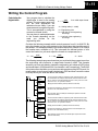
1
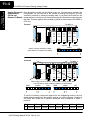
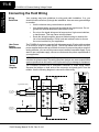
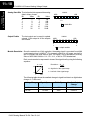
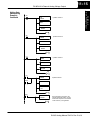
F2-08DA-2 8-Channel Analog Voltage Output In This Chapter. . . . — Module Specifications — Setting the Module Jumper — Connecting the Field Wiring — Module Operation — Writing the Control Program 11 F2-08DA--2 8-Ch. Voltage Output 11--2 F2-08DA-2 8-Channel Analog Voltage Output Module Specifications The F2-08DA-2 Analog Output module provides several hardware features: S Supports DL230, DL240, DL250--1 and DL260 CPUs (see firmware requirements below). S Analog outputs are optically isolated from the PLC logic. S The module has a removable terminal block, so the module can be easily removed or changed without disconnecting the wiring. S Can update all channels in one scan (DL240, DL250--1 and DL260 only). S Outputs are voltage sourcing. S Outputs can be configured for either of these ranges: 1) 0 to 5 VDC OUT ANALOG 8CH F2-08DA--2 21.6--26.4 140mA ANALOG OUT 0--5VDC 0--10VDC 0V +24V +V1 +V2 +V3 +V4 +V5 +V6 +V7 +V8 F2--08DA--2 2) 0 to 10 VDC Firmware Requirements: To use this module, DL230 CPUs must have firmware version 2.7 or later. To use the pointer method of writing values, DL240 CPUs require firmware version 3.0 or later and DL250 CPUs require firmware version 1.33 or later. DL205 Analog Manual 7th Ed. Rev. B 4/10 F2-08DA--2 F2-08DA-2 8-Channel Analog Voltage Output 11--3 Output Specifications General Specifications Number of Channels 8, single-ended Output Ranges 0 to 5V, 0 to 10V Resolution 12 bit (1 in 4096) Output Type Voltage sourcing Peak Output Voltage 15VDC (clamped by transient voltage suppressor) Load Impedance 1k (0--5V range); 10k 0--10V range) Load Capacitance .01μF maximum Linearity Error (end to end) 1 count (0.025% (0 025% of full scale) maximum Conversion Settling Time 400 μs maximum (full scale change) 4.5ms to 9ms for digital out to analog out Full Scale Calibration Error Full-Scale (offset error included) 12 counts max. @ 25 25C C (77 (77F) F) Offset Calibration Error 3 counts maximum @ 25C ( 77F) Accuracy vs. vs Temperature 57 ppm/_C full scale calibration change (including maximum offset change of 2 counts) Maximum Inaccuracyy 0.3% @ 25C (77F) ( ) 0.45% 0--60C ( 32--140F) PLC Update Rate 1 channel per scan maximum (Multiplexing) 8 channels per scan maximum (Pointer [DL240/DL250--1/260 only]) Digital Outputs / Output Points Required 12 binary data bits, 3 ch. ID bits, 1 output enable bit / 16 (Y) output points required Power Budget Requirement 60 mA @ 5VDC (supplied by base) External Power Supply 24VDC (10%), 140mA (outputs fully loaded) Operating Temperature 0 to 60 C (32 to 140 F) Storage Temperature --20 to 70 C (--4 to 158 F) Relative Humidity 5 to 95% (non-condensing) Environmental Air No corrosive gases permitted Vibration MIL STD 810C 514.2 Shock MIL STD 810C 516.2 Noise Immunity NEMA ICS3--304 One count in the specification table is equal to one least significant bit of the analog data value (1 in 4096). Analog Output Configuration Requirements The F2-08DA-2 analog output requires 16 discrete output points. The module can be installed in any slot of a DL205 system, but the available power budget and discrete I/O points can be limiting factors. Check the user manual for your particular model of CPU and I/O base for more information regarding power budget and number of local, local expanison or remote I/O points. DL205 Analog Manual 7th Ed. Rev. B 4/10 F2-08DA--2 8-Ch. Voltage Output The following tables provide the specifications for the F2-08DA-2 Analog Output Module. Review these specifications to make sure the module meets your application requirements. F2-08DA--2 8-Ch. Voltage Output 11--4 F2-08DA-2 8-Channel Analog Voltage Output Special Placement Requirements (DL230 and Remote I/O Bases) Even though the module can be placed in any slot, it is important to examine the configuration. As you can see in the section on writing the program, you use V-memory locations to extract the analog data. If you place the module so the output points do not start on a V-memory boundary, the instructions cannot access the data. This also applies when module is placed in remote base (D2--RSSS in CPU slot). F2-08DA--2 Correct! Slot 0 Slot 1 Slot 2 Slot 3 Slot 4 16pt Input 8pt Input 16pt Output 16pt Output 8pt Output X0 -X17 X20 -X27 Y0 -Y17 Y20 -Y37 V40500 V40502 V40501 MSB LSB Data is correctly entered so output points start on a V-memory boundary. Y 3 7 Y 2 0 Incorrect F2-08DA--2 Slot 0 MSB Slot 1 Slot 2 Slot 3 Slot 4 16pt Input 8pt Input 16pt Output 8pt Output 16pt Output X0 -X17 X20 -X27 Y0 -Y17 Y20 -Y27 Y30 -Y47 Data is split over two locations, so instructions cannot access data from a DL230 (or when module is placed in a remote base). V40502 V40501 LSB MSB LSB Y Y 5 4 0 7 Y 5 7 Y40 -Y47 Y 4 0 Y Y 3 2 0 7 Y 3 7 Y 2 0 To use the V-memory references required for the multiplexing method, the first output address assigned to the module must be one of the following Y locations. The table also shows the V-memory addresses that correspond to these Y locations. Y Y0 Y20 V V40500 V40501 V40502 V40503 V40504 V40505 V40506 V40507 DL205 Analog Manual 7th Ed. Rev. B 4/10 Y40 Y60 Y100 Y120 Y140 Y160 F2-08DA-2 8-Channel Analog Voltage Output 11--5 The F2-08DA-2 Analog Output module uses a jumper for selecting the 0--5V or 0--10V voltage ranges. This figure shows the jumper location and how to set it for either voltage range. 0 -- 5V 0 -- 10V Top Board Bottom Board Voltage Range and Output Combinations The table lists both possible combinations of voltage ranges and data formats, along with the corresponding jumper settings. Voltage Range Output Data Format Jumpers Setting (top board) 0 to 5V 0--4095 Install 0 to 10V 0--4095 Remove These graphs show the voltage range to output data format relationship for each of the two selections. Ranges 0V -- 5V 0V -- 10V 5V 10V 0V 0V 0 4095 0 4095 DL205 Analog Manual 7th Ed. Rev. B 4/10 F2--08DA--2 8-Ch. Voltage Output Setting the Module Jumper F2-08DA--2 8-Ch. Voltage Output 11--6 F2-08DA-2 8-Channel Analog Voltage Output Connecting the Field Wiring Your company may have guidelines for wiring and cable installation. If so, you should check those before you begin the installation. Here are some general things to consider: S Use the shortest wiring route whenever possible. Wiring Guidelines User Power Supply Requirements S Use shielded wiring and ground the shield at the signal source. Do not ground the shield at both the module and the load. S Do not run the signal wiring next to large motors, high current switches, or transformers. This may cause noise problems. S Route the wiring through an approved cable housing to minimize the risk of accidental damage. Check local and national codes to choose the correct method for your application. The F2-08DA-2 requires a separate field-side power supply. Each module requires 21.6--26.4VDC at up to 140mA current. The DL205 bases have built-in 24 VDC power supplies that provide up to 300mA of current. If you are using only a couple of analog modules, you can use this power source instead of a separate supply. If you want to use a separate supply, choose one that meets the power requirements of your application. WARNING: If you are using 24 VDC output power from the base, make sure you calculate the power budget. Exceeding the power budget can cause unpredictable system operation that can lead to a risk of personal injury or damage to equipment. Wiring Diagram The F2-08DA-2 module has a removable connector to make wiring easier. Squeeze the latches on both ends of the connector and gently pull it from the module. Use the following diagram to connect the field wiring. OUT Internal Module Wiring 21.6--26.4VDC @140mA + -- F2-08DA--2 0 VDC +24 VDC See NOTE 1 Ch 1 load 1K--10K ohms minimum +V1 +5V +15V 0V --15V +V2 NOTE 1: Shields should be connected to to the 0V terminal of the module. DC to DC Converter Typical User Wiring +V3 +V4 Ch 1 Voltage source D to A Converter +V6 Ch 8 Voltage source +V7 Ch 8 load 1K--10K ohms minimum DL205 Analog Manual 7th Ed. Rev. B 4/10 0V +24V +V1 +V2 +V3 +V4 +V5 See NOTE 1 21.6--26.4 140mA ANALOG OUT 0--5VDC 0--10VDC +V8 D to A Converter +V5 +V6 +V7 +V8 F2--08DA--2 ANALOG 8CH 11--7 F2-08DA-2 8-Channel Analog Voltage Output Channel Update Sequence for a DL230 CPU (Multiplexing) Before you begin writing the control program, it is important to take a few minutes to understand how the module processes and represents the analog signals. If you are using multiplexing ladder, you can send one channel of data to the output module on each scan. The module refreshes both field devices on each scan, but you can only get new data from the CPU at the rate of one channel per scan. Since there are eight channels, it can take eight scans to update all channels. However, if you are only using one channel, you can update that channel on every scan. The multiplexing method can also b used for the DL240/250--1/260 CPUs. System Using Multiplex Method (DL230) Scan Read inputs Scan N Channel 1 Scan N+1 Channel 2 Scan N+2 Channel 3 Scan N+3 . . . Channel 4 . . . Scan N+8 Channel 8 Execute Application Program Calculate the data Write data Write to outputs DL205 Analog Manual 7th Ed. Rev. B 4/10 F2-08DA--2 8--Ch. Voltage Output Module Operation F2-08DA--2 8-Ch. Voltage Output 11--8 F2-08DA-2 8-Channel Analog Voltage Output Channel Update Sequence for a DL240, DL250--1 or DL260 CPU (Pointer Method) If you are using pointers (Pointer Method), you can update all channels on every scan. This is because the DL240/250--1/260 CPU supports special V-memory locations that are used to manage the data transfer. This is discussed in more detail in the section on Writing the Control Program. System With DL240/250--1/260 CPU Using Pointer Method Scan Read inputs Scan N Channel 1, 2...8 Scan N+1 Channel 1, 2...8 Scan N+2 Channel 1, 2...8 Scan N+3 Channel 1, 2...8 Scan N+4 Channel 1, 2...8 Execute Application Program Calculate the data Write data Write to outputs DL205 Analog Manual 7th Ed. Rev. B 4/10 11--9 F2-08DA-2 8-Channel Analog Voltage Output You may recall the F2-08DA-2 module requires 16 discrete output points in the CPU. These points provide the data value and an indication of which channel to update. Note, if you are using a DL240/250--1/260 CPU, you may never have to use these bits, but it may help you understand the data format. Since all output points are automatically mapped into V-memory, it is very easy to determine the location of the data word that will be assigned to the module. F2-08DA--2 Slot 0 Slot 1 Slot 2 Slot 3 Slot 4 16pt Input 8pt Input 16pt Output 16pt Output 8pt Output X0 -X17 X20 -X27 Y0 -Y17 Y20 -Y37 Y40 -Y47 V40500 V40502 V40501 LSB MSB Y YYY 3 3 3 3 7 6 5 4 Y 2 0 Data Bits Within this word location, the individual bits represent specific information about the analog signal. Channel Select Outputs Three of the outputs select the active channel. Remember, the V-memory bits are mapped directly to discrete outputs. The binary weight of these three bits determines the selected channel. By controlling these outputs, you can select which channel gets updated. V40501 MSB LSB YY Y 3 3 3 6 5 4 Y 2 0 = channel select outputs Y36 Y35 Y34 Channel Number Selected 1 X X X 2 3 X X 4 5 X X X X X X 6 7 X 8 DL205 Analog Manual 7th Ed. Rev. B 4/10 F2--08DA--2 8-Ch. Voltage Output Understanding the Output Assignments F2-08DA--2 8-Ch. Voltage Output 11--10 F2-08DA-2 8-Channel Analog Voltage Output Analog Data Bits The first twelve bits represent the analog data in binary format. Bit Value Bit Value 0 1 6 64 1 2 7 128 2 4 8 256 3 8 9 512 4 16 10 1024 5 32 11 2048 Output Enable The last output can be used to update outputs. If this output is off the outputs are cleared. V40501 MSB LSB 11 9 8 7 6 5 4 3 2 1 0 10 = data bits V40501 MSB LSB Y 3 7 Y 2 0 = output enable Module Resolution Since the module has 12-bit resolution, the analog signal is converted from 4096 counts ranging from 0--4095 (212). For example, with a 0 to 10V range, send a 0 to get a 0V signal, and send 4095 to get a 10V signal. This is equivalent to a binary value of 0000 0000 0000 to 1111 1111 1111, or 000 to FFF hexadecimal. Each count can also be expressed in terms of the signal level by using the following equation: 0 -- 10V Resolution = H − L 4095 10V H = high limit of the signal range L = low limit of the signal range 0V 0 4095 The following table shows the smallest change in signal level due to a digital value change of 1 LSB count. Voltage Range Signal Span Divide By Smallest Output Change 0 to 5V 5 volts 4095 1.22 mV 0 to 10V 10 volts 4095 2.44 mV DL205 Analog Manual 7th Ed. Rev. B 4/10 11--11 F2-08DA-2 8-Channel Analog Voltage Output Calculating the Digital Value Your program has to calculate the digital value to send to the analog module. There are many ways to do this, but most applications are understood more easily if you use measurements in engineering units. This is accomplished by using the conversion formula shown. You may have to make adjustments to the formula depending on the scale you choose for the engineering units. A = U 4095 H−L for 0--4095 output format A = Analog value (0 -- 4095) U = Engineering units H = High limit of the engineering unit range L = Low limit of the engineering unit range Consider the following example which controls pressure from 0.0 to 99.9 PSI. By using the formula you can easily determine the digital value that should be sent to the module. The example shows the conversion required to yield 49.4 PSI. Notice the formula uses a multiplier of 10. This is because the decimal portion of 49.4 cannot be loaded, so you must adjust the formula to compensate for it. A = 10U 4095 10(H − L) A = 494 4095 1000 − 0 A = 2023 The following example program shows how you would write the program to perform the engineering unit conversion to output data formats 0--4095. This example assumes you have calculated or loaded the engineering unit values in BCD format and stored them in V2300 and V2301 for channels 1 and 2 respectively. The DL205 offers instructions that allow you to perform math operations using BCD format. It is usually easier to perform any math calculations in BCD and then convert the value to binary before you send the data to the module. SP1 SP1 LD V2300 The LD instruction loads the engineering units used with channel 1 into the accumulator. This example assumes the numbers are BCD. Since SP1 is used, this rung automatically executes on every scan. You could also use an X, C, etc. permissive contact. MUL K4095 Multiply the accumulator by 4095 (to start the conversion). DIV K1000 Divide the accumulator by 1000 (because we used a multiplier of 10, we have to use 1000 instead of 100). OUT V2000 Store the BCD result in V2000 (the actual steps required to send the data are shown later). LD V2301 The LD instruction loads the engineering units used with channel 2 into the accumulator. This example assumes the numbers are BCD. Since SP1 is used, this rung automatically executes on every scan. You could also use an X, C, etc. permissive contact. MUL K4095 DIV K1000 OUT V2001 Multiply the accumulator by 4095 (to start the conversion). Divide the accumulator by 1000 (because we used a multiplier of 10, we have to use 1000 instead of 100). Store the BCD result in V2001 (the actual steps required to send the data are shown later). DL205 Analog Manual 7th Ed. Rev. B 4/10 F2--08DA--2 8-Ch. Voltage Output Writing the Control Program F2-08DA--2 8-Ch. Voltage Output 11--12 F2-08DA-2 8-Channel Analog Voltage Output Writing Values: Pointer Method and Multiplexing Pointer Method Example 230 240 250-- 1 260 There are two methods of reading values: S The pointer method S Multiplexing method You can use either method when using DL240, DL250--1 and DL260 CPUs, but for ease of programming it is strongly recommended that you use the pointer method. You must use the multiplexing method when using DL230 CPUs and with remote I/O modules (the pointer method will not work). Once you have calculated the data values (shown previously) you must enter the program that actually updates the module. The DL240/250--1/260 has special V-memory locations assigned to each base slot that greatly simplify the programming requirements. By using these V-memory locations you can: S specify the number of channels to update. S specify where to obtain the output data . NOTE: DL240 CPUs with firmware release version 3.0 or later and DL250 CPUs with firmware release 1.33 are required to support this method. The following program example shows how to setup these locations. Place this rung anywhere in the ladder program, or in the initial stage if you are using stage programming. You may recall in the previous example we used V2000 through V2007 to store the calculated values. Also, in the previous examples we had the analog module installed in slot 3. You should use the appropriate memory locations for your application. The pointer method automatically converts values to binary. SP0 LD K8 - or - LD K 88 Loads a constant that specifies the number of channels to scan and the data format. The lower byte, most significant nibble (MSN) selects the data format (0=BCD, 8=Binary), the LSN selects the number of channels (1--8). The binary format is used for displaying data on some operator interfaces. The DL230/240 CPUs do not support binary math functions, whereas the DL250 does. OUT V7663 Special V-memory location assigned to slot 3 that contains the number of channels to scan. LDA O2000 This loads an octal value for the first V-memory location that will be used to store the output data. For example, the O2000 entered here would designate the following addresses: Ch1 -- V2000, Ch 2 -- V2001.....Ch8 -- V2007 OUT V7703 The octal address (O2000) is stored here. V7703 is assigned to slot 3 and acts as a pointer, which means the CPU will use the octal value in this location to determine exactly where to store the output data. DL205 Analog Manual 7th Ed. Rev. B 4/10 11--13 F2-08DA-2 8-Channel Analog Voltage Output The Table below applies to the DL240, DL250--1 and DL260 CPU base. CPU Base: Analog Output Module Slot-Dependent V-memory Locations Slot 0 1 2 3 4 5 6 F2-08DA--2 8--Ch. Voltage Output The tables below show the special V-memory locations used by the DL240, DL250--1 and DL260 for the CPU base and local expansion base I/O slots. Slot 0 (zero) is the module next to the CPU or D2--CM module. Slot 1 is the module two places from the CPU or D2--CM, and so on. Remember, the CPU only examines the pointer values at these locations after a mode transition. Also, if you use the DL230 (multiplexing) method, verify that these addresses in the CPU are zero. 7 No. of Channels V7660 V7661 V7662 V7663 V7664 V7665 V7666 V7667 Storage Pointer V7700 V7701 V7702 V7703 V7704 V7705 V7706 V7707 The Table below applies to the DL250--1 or DL260 expansion base 1. Expansion Base D2--CM #1: Analog Output Module Slot-Dependent V-memory Locations Slot 0 1 2 3 4 5 6 7 No. of Channels V36000 V36001 V36002 V36003 V36004 V36005 V36006 V36007 Storage Pointer V36020 V36021 V36022 V36023 V36024 V36025 V36026 V36027 The Table below applies to the DL250--1 or DL260 expansion base 2. Expansion Base D2--CM #2: Analog Output Module Slot-Dependent V-memory Locations Slot 0 1 2 3 4 5 6 7 No. of Channels V36100 V36101 V36102 V36103 V36104 V36105 V36106 V36107 Storage Pointer V36120 V36121 V36122 V36123 V36124 V36125 V36126 V36127 The Table below applies to the DL260 CPU expansion base 3. Expansion Base D2--CM #3: Analog Output Module Slot-Dependent V-memory Locations 0 1 2 3 4 5 6 7 No. of Channels V36200 V36201 V36202 V36203 V36204 V36205 V36206 V36207 Storage Pointer V36220 V36221 V36222 V36223 V36224 V36225 V36226 V36227 The Table below applies to the DL260 CPU expansion base 4. Expansion Base D2--CM #4: Analog Output Module Slot-Dependent V-memory Locations Slot 0 1 2 3 4 5 6 7 No. of Channels V36300 V36301 V36302 V36303 V36304 V36305 V36306 V36307 Storage Pointer V36320 V36321 V36322 V36323 V36324 V36325 V36326 V36327 DL205 Analog Manual 7th Ed. Rev. B 4/10 Installation and Safety Guidelines Slot F2-08DA--2 8-Ch. Voltage Output 11--14 F2-08DA-2 8-Channel Analog Voltage Output Writing Data (Multiplexing) 230 The following example shows how to write data using the mutliplexing method. C10 C0 OUT 240 250-- 1 260 C7 LD V2007 Restarts the update sequence. Updates channel 8. BIN ORD K7000 C10 OUT C6 LD V2006 Updates channel 7. BIN ORD K6000 C7 OUT C5 LD V2005 Updates channel 6. BIN ORD K5000 C6 OUT C4 LD V2004 Updates channel 5. BIN ORD K4000 C5 OUT Continued DL205 Analog Manual 7th Ed. Rev. B 4/10 F2-08DA-2 8-Channel Analog Voltage Output C3 LD V2003 Updates channel 4. BIN ORD K3000 C4 OUT C2 LD V2002 Updates channel 3. BIN ORD K2000 C3 OUT C1 LD V2001 Updates channel 2. BIN ORD K1000 C2 OUT C0 SP0 LD V2000 Updates channel 1. BIN ORD K0 C1 OUT SP1 OUT V40501 Y37 OUT Sends the data to the module. Our example starts with V40501, but the actual value depends on the location of the module in your application. DL205 Analog Manual 7th Ed. Rev. B 4/10 F2-08DA--2 8--Ch. Voltage Output Writing Data (Multiplexing Example) Continued 11--15 F2-08DA--2 8-Ch. Voltage Output 11--16 F2-08DA-2 8-Channel Analog Voltage Output Sending Data to One Channel If you are using more than one channel, or if you want to control the updates separately, use the following program. SP1 LD V2000 The LD instruction loads the data into the accumulator. Since SP1 is used, this rung automatically executes on every scan. You could also use an X, C, etc. permissive contact. BIN The BIN instruction converts the accumulator data to binary (you must omit this step if you have already converted the data elsewhere). ANDD K0FFF The ANDD instruction masks off the channel select bits to prevent an accidental channel selection. OUT V40501 The OUT instruction sends the data to the module. Our example starts with V40501, but the actual value depends on the location of the module in your application. Y34 RST Y34, Y35, Y36--OFF selects channel 1 for updating. Y35 RST Y36 RST Y37 OUT Analog and Digital Value Conversions Y37 is the output enable bit. Sometimes it is useful to be able to quickly convert between the signal levels and the digital values. This is especially helpful during machine startup or troubleshooting. The following table provides formulas to make this conversion easier. Remember, if you embed the sign information into the data value, you must adjust the formulas accordingly. Range If you know the digital value ... If you know the signal level ... 0 to 10V A = 10D 4095 D = 4095 (A) 10 0 to 5V A = 5D 4095 D = 4095 (A) 5 For example, if you are using the 0--10V range and you know you need a 6V signal level, use this formula to determine the digital value (D) that will be stored in the V-memory location that contains the data. D = 4095 (A) 10 D = 4095 (6V) 10 D = (409.5) (6) D = 2457 DL205 Analog Manual 7th Ed. Rev. B 4/10