1
SingMai Electronics
PT22
Advanced Composite
Video Interface:
Decoder
User Manual
Revision 0.5
30th June 2014
PT22 User Manual Revision 0.5
Page 1 of 28
SingMai Electronics
Revision History
Date
21-02-2013
30-06-2014
Revisions
First Draft.
Document re-written.
PT22 User Manual Revision 0.5
Version
0.1
0.5
Page 2 of 28
SingMai Electronics
Contents
Revision History ......................................................................................................................... 2
Contents .................................................................................................................................... 3
Tables ........................................................................................................................................ 3
Figures ....................................................................................................................................... 3
1.
Introduction ....................................................................................................................... 4
2.
PT22 Module description .................................................................................................. 5
3.
Signal Interconnections..................................................................................................... 6
4.
aCVi Overview .................................................................................................................. 9
5.
Technical Overview ......................................................................................................... 11
aCVi_decoder.v ................................................................................................................... 11
aCVi_Rx_Register_control.v ............................................................................................... 11
aCVi_Demod.v .................................................................................................................... 12
aCVi_DemodLPF.v.............................................................................................................. 13
aCVi_SPG.v ........................................................................................................................ 14
aCVi_Comb_filter.v ............................................................................................................. 16
aCVi_measure.v .................................................................................................................. 16
aCVi_Procamp.v ................................................................................................................. 17
aCVi_data.v ......................................................................................................................... 17
aCVi_Chargen.v .................................................................................................................. 19
6.
Register interface ............................................................................................................ 23
7.
Register descriptions ...................................................................................................... 24
8.
PGA amplifier control ...................................................................................................... 27
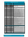
Tables
Table 1 PT22 Altera FPGA resource requirements................................................................... 4
Table 2 PT22 Verilog file structure ............................................................................................ 5
Table 3 PT22 Input/Output signals ............................................................................................ 7
Table 4 SC10 Line and subcarrier frequencies ....................................................................... 12
Table 5 Data transfer instructions: Receiver > Transmitter ..................................................... 18
Table 6 aCVi Control words Transmitter > Receiver ............................................................... 18
Table 7 Character generator map. .......................................................................................... 21
Table 8 Register description .................................................................................................... 26
Figures
Figure 1 PT22 Block symbol. ..................................................................................................... 6
Figure 2 aCVi Spectrum. ......................................................................................................... 10
Figure 3 PT22 Block diagram .................................................................................................. 11
Figure 4 Chroma demodulator low pass filter. ......................................................................... 14
Figure 5 Sync filter frequency response. ................................................................................. 14
Figure 6 Phase detector low pass filter response ................................................................... 15
Figure 7 External VCO schematic ........................................................................................... 16
Figure 8 aCVi Data format. ...................................................................................................... 17
Figure 9 Character overlay address map. ............................................................................... 19
Figure 10 Character mapping .................................................................................................. 22
Figure 11 PT22 Register timing ............................................................................................... 23
Figure 12 AD8337 PGA gain response ................................................................................... 27
Figure 13 PWM analogue control. ........................................................................................... 28
PT22 User Manual Revision 0.5
Page 3 of 28
SingMai Electronics
1. Introduction
PT22 is a decoder IP (intellectual property) core compatible with the aCVi Advanced
Composite Video Interface.
aCVi is a method to transmit HD video over existing RG-59/UTP coaxial/twisted-pair cable
networks or allow the use of less expensive RG-59/UTP coaxial/twisted-pair cable in long
distance
installations.
Details
on
the
interface
may
be
found
here:
http://www.singmai.com/acvi/aCVi_technology.htm.
The decoder IP accepts digital aCVi encoded video at 10 bit resolution, which it decodes to a
20 bit YCbCr (BT601 format) output with separate horizontal and vertical synchronizing
pulses and 74.25MHz clock. PT22 supports 720p/50Hz, 720p/60Hz, 1080p/25Hz,
1080p/30Hz, 1080p/50Hz and 1080p/60Hz but may also be readily adapted to other
standards and also non-standard video formats such as VESA formats.
Control and status registers are written to and read from using a conventional 8 bit wide
microprocessor interface.
The intellectual property block is provided as RTL compliant Verilog-2001 source code for
FPGAs from all vendors or for ASICs.
Typical resource usage for an Altera FPGA is shown in Table 1.
Logic Cells
Memory Bits
M9K blocks
9x9 Multipliers
10375
349952
44
0
18x18
multipliers
8
Table 1 PT22 Altera FPGA resource requirements
An approximate equivalent for ASIC resource usage is 11623 LCs (including multipliers) x 14
= 162722 2 input NAND gate equivalent. The memory is single port ROM and RAM.
PT22 User Manual Revision 0.5
Page 4 of 28
SingMai Electronics
2. PT22 Module description
The PT22 aCVi decoder IP core comprises 14 Verilog modules in a hierarchical structure,
(see Table 2).
aCVi_decoder.v
aCVI_
Rx_Register_
control.v
aCVi_
Demod.v
aCVI_
DemodLPF.
v
aCVi_
SPG.v
aCVi_
data.v
aCVi_
Comb_
filter.v
Rx_SinCos
_ ROM.v
Chargen.v
aCVi_
Proca
mp.v
aCVi_
Measure.
v
Char_Disp_
RAM.v
Char_Disp_
ROM.v
CG_ROM.v
Table 2 PT22 Verilog file structure
The top level file is aCVi_decoder.v which, in turn, calls nine of the other modules.
aCVi_Demod.v calls a third level file, Rx_SinCos_ROM.v. Chargen.v (the character overlay)
call three other modules.
PT22 User Manual Revision 0.5
Page 5 of 28
SingMai Electronics
3. Signal Interconnections
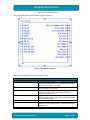
The PT22 signal interconnect diagram is shown in Figure 1.
Figure 1 PT22 Block symbol.
The signal descriptions are shown in Table 3, below.
Signal
Clk74
Clk148
Reg_Clk
RESETn
ORNG
aCVi_in[9:0]
A[8:0]
PT22 User Manual Revision 0.5
Inputs
Description
74.25MHz clock input from VCO. All outputs are valid
on the rising edge of this clock. Rising edges of Clk74
and Clk148 should be coincident.
148.5MHz clock from VCO. . Rising edges of Clk74 and
Clk148 should be coincident.
Clock used for writing to the control registers only. If
‘Clk74’ is continuous and stable Reg_clk may be
connected to this input.
Asynchronous active low reset signal. Asserting this
input sets all the control registers to their default value
and resets all registers.
Over-range input from the ADC.
Input aCVI encoded data from ADC. Data should be
valid on the rising edge of Clk74. This input should be
offset binary.
Address bus input used to select the control
Page 6 of 28
SingMai Electronics
register/character generator location to be written
to/read from.
Control data input bus.
Control chip select input, active low. Used in
combination with the WRn input to control writing to the
control registers.
Character overlayl chip select input, active low. Used in
combination with the WRn input to control writing to the
character overlay memory.
Active low write enable input. Used in combination with
the CSn input to control writing to the control registers
and character overlay.
Outputs
Description
Din[7:0]
aCVi_Rx_CSn
aCVi_CG_CSn
aCVi_Rx_WRn
Signal
aCVi_Rx_Register_out[7..0]
Control output data bus. Outputs the control/status
register data selected by the A[7:0] bus. (Note: the
character overlay is write only)
Y (luma) output from the encoder. The output is straight
binary, blanking level is 6410 and peak level 96010. The
data output is valid at the rising edge of Clk74.
aCVi_Yout[9] is the MSB.
Cb (B-Y chroma) output from the encoder. The output is
offset binary, blanking level is 51210. The data output is
valid at the rising edge of Clk74 when aCVi_Cmux is
high (37.125MHz data rate: 4:2:2 format).
aCVi_Cbout[9] is the MSB.
Cr (R-Y chroma) output from the encoder. The output is
offset binary, blanking level is 51210. The data output is
valid at the rising edge of Clk74 when aCVi_Cmux is
high (37.125MHz data rate: 4:2:2 format).
aCVi_Crout[9] is the MSB.
Data valid output for Cb and Cr outputs. Cb and Cr data
is valid on the rising edge of Clk74 when aCVi_Cmux is
high (4:2:2 data format).
Horizontal sync output from decoder (active low).
Vertical sync output from decoder (active low).
Frame sync output from decoder (low for field 1). Only
valid during interlaced video formats.
Horizontal blanking output from decoder.
Vertical blanking output from decoder.
Pulse width modulated output for the control of the
analogue input stage voltage controlled amplifier (AGC).
Pulse width modulated output for the control of external
voltage controlled oscillator frequency (VCO control
voltage).
Test outputs. Do not connect.
aCVi_Yout[9:0]
aCVi_Cbout[9:0]
aCVi_Crout[9:0]
aCVi_Cmux
aCVi_Hout
aCVi_Vout
aCVi_Fout
aCVi_HBlank
aCVi_VBlank
Gain_control
VCO_PWM
aCVi_test[1:0]
Table 3 PT22 Input/Output signals
The Verilog instantiation of PT22 is shown below:
// Instantiate aCVi decoder (PT22)
aCVi_decoder aCVi_decoder_inst
(
.Clk74(Clk74_sig) ,
.Clk148(Clk148_sig) ,
.Reg_clk(Reg_clk_sig) ,
.RESETn(RESETn_sig) ,
PT22 User Manual Revision 0.5
// input
// input
// input
// input
Clk74_sig
Clk148_sig
Reg_clk_sig
RESETn_sig
Page 7 of 28
SingMai Electronics
.ORNG(ORNG_sig) ,
.aCVi_in(aCVi_in_sig) ,
.A(A_sig) ,
.Din(Din_sig) ,
.aCVi_Rx_CSn(aCVi_Rx_CSn_sig) ,
.aCVi_CG_CSn(aCVi_CG_CSn_sig) ,
.aCVi_Rx_WRn(aCVi_Rx_WRn_sig) ,
.aCVi_Rx_Register_out(aCVi_Rx_Register_out_sig) ,
.aCVi_Yout(aCVi_Yout_sig) ,
.aCVi_CbCrout(aCVi_CbCrout_sig) ,
.aCVi_Cmux(aCVi_Cmux_sig) ,
.aCVi_Hout(aCVi_Hout_sig) ,
.aCVi_Vout(aCVi_Vout_sig) ,
.aCVi_Fout(aCVi_Fout_sig) ,
.aCVi_HBlank(aCVi_HBlank_sig) ,
.aCVi_VBlank(aCVi_VBlank_sig) ,
.Data_out(Data_out_sig) ,
.Gain_control(Gain_control_sig) ,
.VCO_PWM(VCO_PWM_sig) ,
.aCVi_test(aCVi_test_sig)
// input ORNG_sig
// input [9:0] aCVi_in_sig
// input [8:0] A_sig
// input [7:0] Din_sig
// input aCVi_Rx_CSn_sig
// input aCVi_CG_CSn_sig
// input aCVi_Rx_WRn_sig
// output [7:0] aCVi_Rx_Register_out_sig
// output [9:0] aCVi_Yout_sig
// output [9:0] aCVi_CbCrout_sig
// output aCVi_Cmux_sig
// output aCVi_Hout_sig
// output aCVi_Vout_sig
// output aCVi_Fout_sig
// output aCVi_HBlank_sig
// output aCVi_VBlank_sig
// output Data_out_sig
// output Gain_control_sig
// output VCO_PWM_sig
// output [1:0] aCVi_test_sig
);
PT22 User Manual Revision 0.5
Page 8 of 28
SingMai Electronics
4. aCVi Overview
The following is a brief overview of the aCVi interface.
The basic concept of the aCVi interface is to build on the proven and reliable transport
method of NTSC, (the advantages of PAL – v.v. multi-path reception – is not relevant to a
cable system so NTSC is used as the model). NTSC transmissions are capable of more than
1km across RG-59 cable but the bandwidth is limited to 5MHz. NTSC also has chroma/luma
crosstalk issues that are difficult to resolve at the receiver end.
Because the cable system is a closed system, it is only necessary for the transmitter and
receiver to ‘understand’ each other and we can modify the basic NTSC method to suit HD
transmissions.
The first thing to overcome is the bandwidth restrictions of the cable. HD 720p/60Hz
transmission requires a luma bandwidth of 30MHz according to the SMPTE-296M. Because
we have only a single coaxial cable for the transport we have chosen to transmit luma and
colour difference signals, (as opposed to component red, green blue), as the colour difference
signals, because of the visual perception of the eye being less acute to colour, can be sent at
half or less of the luma bandwidth: i.e. 7.5Hz each.
As we are transmitting video for a complete system, from camera to DVR or monitor, we
should take into account system bandwidth limitations such as the Kell factor and the camera
Bayer colour filter. The luma bandwidth may be set to either 30MHz (default) or 12MHz. The
chroma bandwidth is set to 7.5MHz which produces no visible degradation of the image.
To further reduce the bandwidth of the transmission the colour difference signals are
modulated onto a carrier in quadrature so they effectively use the same bandwidth. However,
to minimise the signal recovery problems of NTSC, (and as we have no backward
compatibility issues), the upper sideband of the chroma and the luma baseband do not
overlap; for 720p/60Hz transmission the carrier is ~24.7Hz.
The effective bandwidth of the complete signal is therefore approximately 9.3MHz (chroma
upper sideband + filter roll off) + 24.7MHz or about 34MHz, setting a minimum sampling
frequency of 2 x 34MHz or 68MHz. For convenience we choose 74.25MHz as a sampling
frequency as this is related to the 720p/60 SMPTE standard; (see Figure 12).
For 300m of RG-59 cable we can expect 18dB loss at this frequency (6.2dB/100m @
50MHz). However the synchronizing signals are at a much lower frequency where the loss is
only about 1-2dB so reliable rastering of the received signal should always be assured.
To simplify the high frequency compensation of the transmission pre-emphasis is used. The
degree of pre-emphasis is programmable to allow for different cable lengths. The maximum
pre-emphasis is set at 40dB and the frequency response is set to approximate the cable
characteristics.
A further improvement in the SNR is achieved through transmitting a peak to peak video level
of 1.5V which maintains compatibility with any legacy SD equipment on the network and also
allows common low-power 5V drivers to be used.
PT22 User Manual Revision 0.5
Page 9 of 28
SingMai Electronics
Figure 2 aCVi Spectrum.
At extreme distances the bandwidth will start to further fall off. The chroma signal will be the
first affected by this being the highest frequency component. However automatic colour
control in the receiver can maintain the colour saturation over a further ~9dB signal
attenuation. The luma bandwidth will be ‘gracefully’ reduced as the distance is increased.
Because of the similarity in the transmission method to NTSC both the transmitter and
receiver can easily be made to accommodate conventional NTSC/PAL transmissions.
ACVi also allows for the bidirectional transfer of
byte of data is transmitted in each direction per
depending on the video frame rate). The data
effects of cable attenuation. Data is sent using
interval.
PT22 User Manual Revision 0.5
data between receiver and transmitter. One
frame (i.e. 50 or 60 bytes/second data rate
rate is deliberately kept low to reduce the
two dedicated lines in the vertical blanking
Page 10 of 28
SingMai Electronics
5. Technical Overview
A simplified block diagram of the PT22 aCVi decoder is shown in Figure 2.
Figure 3 PT22 Block diagram
The aCVi input from the ADC is a straight binary, 10-bit input sampled at 74.25MHz.
Analogue clamping prior to the ADC ensure the most negative value of the input signal (the
sync tips) are clamped to the negative reference of the ADC (code value 0).
The following is a brief description of each Verilog module.
aCVi_decoder.v
This is the top level module for the PT22. It provides the interconnection between all the other
modules.
aCVi_Rx_Register_control.v
A conventional 8 bit microprocessor style control is used to write and read to the PT22 control
registers. Details of the interface may be found in Chapter 5 and the register descriptions may
be found in Chapter 6.
PT22 User Manual Revision 0.5
Page 11 of 28
SingMai Electronics
aCVi_Demod.v
A free-running subcarrier frequency is generated using a 32 bit ratio counter clocked from the
input 74.25MHz clock.
ratio
Fsc
θ sc subcarrier seed
phase change per line
pixels per line
74.25 MHz 360
232
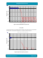
The free-running frequency of the subcarrier is depends on the colour standard; (see table 5).
Format
720p/60
720p/50
720p/30
720p/25
1080p/30
1080p/25
1080p/24
1080i/30
1080i/25
Pixels/line
1650
1980
3300
3960
2200
2640
2750
2200
2640
Line frequency
45.00kHz
37.50kHz
22.50kHz
18.75kHz
33.75kHz
28.125kHz
27.00kHz
33.75kHz
28.125kHz
FSC/FH ratio
549.5
659.5
1097.5
1317.5
731.5
879.5
915.5
731.5
879.5
Subcarrier
24.7275MHz
24.73125MHz
24.69375MHz
24.703125MHz
24.688125MHz
24.7359375MHz
24.7185MHz
24.688125MHz
24.7359375MHz
Seed value
55417954H
5544C8A9H
5523AF52H
552BF5A8H
551EB851H
5548EBD4H
553987BAH
551EB851H
5548EBD4H
Table 4 SC10 Line and subcarrier frequencies
The top 11 bits of this ratio counter (the phase word) are used by the demodulator to generate
the sine and cosine waveforms.
For the demodulation to correctly operate the generated subcarrier must be frequency and
phase locked to the aCVi video subcarrier which is done by measuring the amplitude of the
demodulated and low pass filtered V output during the colour burst. If the frequency and
phase of the free-running subcarrier and the colour burst are the same then this error will be
zero. The reference for the BLO is the demodulated and filtered V output from the
demodulator low pass filter. 32 samples of this waveform are taken during the burst pulse; the
burst gate pulse from the SPG is used for this purpose.
The seed word is thus modified using the phase error signal until the input colour burst and
the ratio counter are phase locked.
The aCVi chroma signal is originally generated as follows:
chroma U sinωt V cosωt
When the burst lock loop (BLO) is in lock, the frequency and phase will be the same as when
the signal was being modulated. Thus, multiplying the aCVi composite video by the sine and
cosine of the same frequency and phase gives the following:
U ' U sin ωt V cos ωt sin ωt
U ' U sin 2 ωt V sin ωt cos ωt
1 cos 2 ωt V
U ' U
2 2 sin ωt cos ωt
2
U '
U U cos 2 ωt V sin 2 ωt
2
2
2
PT22 User Manual Revision 0.5
Page 12 of 28
SingMai Electronics
…and for the V component:
V ' U sin ωt V cos ωt cos ωt
V ' U sin ωt cos ωt V cos 2 ωt
V '
U
1 cos 2 ωt
2 sin ωt cos ωt V
2
2
V '
U sin 2 ωt V V cos 2 ωt
2
2
2
The lower 9 bits of the 11-bit phase output from the BLO, (burst locked oscillator), are used to
address a sine and cosine lookup table. These 9 bits comprise the phase angle, at subcarrier
frequency, within a single quadrant and the top two bits are the quadrant – this method save
memory by only requiring a single quadrant to be stored in the LUT. The output of the Sin/Cos
LUT is a 24 bit word; 12 bits cosine and 12 bits sine. The quadrant signs are used to
manipulate the sine and cosine data such as to construct a full waveform.
The reconstructed sine and cosine waveforms are then multiplied by the input 74.25MHz freerunning composite video. The output of the sine channel is the demodulated U signal and the
cosine is the demodulated V output. One over-range bit caters for at the output to allow for
twice subcarrier frequency components, (removed by the subsequent low pass filter).
aCVi_DemodLPF.v
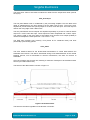
The output of the demodulator also comprises twice subcarrier frequencies. The output is
therefore low pass filtered using a 63 tap filter, the response for which is shown in Figure 4.
The output of the filter is the clean ‘simple’ demodulated U and V.
PT22 User Manual Revision 0.5
Page 13 of 28
SingMai Electronics
In p h a s e F ilt e r F r e q u e n c y R e s p o n s e
Magnitude in dB
0
-20
-40
-60
-80
0
4
8
12
16
20
F r e q u e n c y in M H z
Figure 4 Chroma demodulator low pass filter.
aCVi_SPG.v
The luma output from the comb filter (with the subcarrier removed) is further low pass filtered
to reduce noise. The response of this filter, an 11 tap FIR, is shown in Figure 5.
In p h a s e F ilt e r F r e q u e n c y R e s p o n s e
20
Magnitude in dB
0
-20
-40
-60
0
4
8
12
16
20
24
28
F r e q u e n c y in M H z
Figure 5 Sync filter frequency response.
PT22 User Manual Revision 0.5
Page 14 of 28
SingMai Electronics
A fixed offset is subtracted from the low pass filtered luma video such that the midpoint of the
sync pulse is at value 0. Values 1-44 from the horizontal counter address a look up table
whose output coefficients form a FIR low pass filter to further reduce noise from the
composite video. The coefficients are multiplied by the offset video and accumulated across
the 44 samples, being updated once per horizontal line. The frequency response of the sync
filter is shown in Figure 6.
In p h a s e F ilt e r F r e q u e n c y R e s p o n s e
10
0
Magnitude in dB
-10
-20
-30
-40
-50
-60
0
4
8
F r e q u e n c y in M H z
Figure 6 Phase detector low pass filter response
When the midpoint of the falling edge of the horizontal pulse is coincident with the centre tap
of the FIR filter the accumulated result will be zero. When they are not coincident an error will
be generated.
This error is filtered using a recursive filter (integrator) and proportional and integral terms are
added to create an error word which is converted to a PWM signal to control and external
voltage controlled oscillator (VCO). (See Figure 7).
The horizontal pixel counter is used by the SPG, (sync pulse generator), to provide the
horizontal timing pulses required by the decoder, including the black level clamp pulse to the
analogue front end and the burst gate pulse for the demodulator.
The vertical field pulses are recovered by using a digital integrator on the sliced composite
video.
PT22 User Manual Revision 0.5
Page 15 of 28
SingMai Electronics
Figure 7 External VCO schematic
aCVi_Comb_filter.v
The upper luma frequencies and the lower sideband of the chroma overlap. Although there is
very little luma energy in this region for most applications it is still better to completely
separate them. This can separated because the chroma information has a known line based
phase relationship whereas the HF luma and cross colour does not. The comb filter provides
this filtering operation.
A line comb filter is used which has an aperture of 3 lines: (1/4*0H + 1/2*1H + 1/4*2H) (1 line
spacing). For the comb filter to operate correctly the phase relationship of the colour
component must be maintained. If not the HF luma will not be cancelled and can even be
reinforced. It is therefore necessary to detect when the comb filter fails and switch to another
mode. Normally this failure mode is detected using luminance differences across the comb
taps but there are instances where the same luminance value can occur but there are
different chroma values which still cause the comb to fail. The SC10 comb adaptation detects
value differences in luma, U and V comb taps thereby detecting all comb failure instances.
The output of the comb filter is combed U and V without high frequency luma.
The combed chroma signal is then frequency shifted back to the subcarrier frequency and
subtracted from the low pass filtered aCVi video.
The sine and cosine waveforms from the demodulator are delayed to compensate for the low
pass filter delay; the waveforms are then multiplied by the combed U and V outputs and then
added together to reconstruct a chrominance signal centred on the aCVi referenced
subcarrier frequency. This chrominance signal is then subtracted from the delayed low pass
filtered luma video which provides a clean luma signal with no residual chroma.
aCVi_measure.v
The aCVi decoder makes a number of measurements of the video signal to aid in it automatic
adaption and to provide control of the transmitter pre-emphasis and luma and chroma
automatic gain controls.
The luminance measurements are performed on the low pass filtered video from the sync
filter.
The back porch value and the most negative video amplitude values are used to calculate the
sync pulse amplitude which in turn is used to control the gain of the analogue programmable
gain amplifier.
PT22 User Manual Revision 0.5
Page 16 of 28
SingMai Electronics
The back porch value is also used to subtract an offset from the output luma value (remove
the syncs).
aCVi_Procamp.v
The low pass filtered luma is conditioned by the processing amplifier. First the black level
offset is subtracted from the luma signal to set the black level at zero. The luma is then
amplified to provide a 960 code (10 bit) output for a 100% colour bar input. The luma output is
valid on the rising edge of the 74MHz clock.
The low pass filtered chroma outputs are amplified separately to provide a nominal 700mV
output for a 100% colour bar input. These outputs are then multiplexed into a Cb/Cr output.
The output is valid on the rising edge of the 74MHz clock and the Cmux output (37MHz) is
used to de-multiplex the video (Cmux=0 = Cb, Cmux=1 = Cr).
The SPG also provides Vout (vertical), Fout (frame ID for interlaced video) and Hout
(horizontal) synchronizing pulses.
aCVi_data.v
The aCVi interface allows for the bi-directional transmission of control data between the
transmitter and receiver. The data is transferred during to two dedicated lines of the vertical
blanking interval, one for transmitter to receiver transmission, the other for receiver to
transmitter.
One byte of data is sent for each line, allowing a maximum of 60 bytes to be transferred each
second, (for a 60Hz frame rate).
The format of the data transfer is shown in Figure 17.
Figure 8 aCVi Data format.
The format is the same regardless of the direction of transfer.
PT22 User Manual Revision 0.5
Page 17 of 28
SingMai Electronics
The first 8 bits are the framing byte which is a unique code signifying the beginning of data.
The receiving device must monitor the pre-defined vertical blanking line for this framing byte
which is a unique code.
The next four bits are a control word which defines the function of the following data byte. The
control words between transmitter and receiver and receiver and transmitter are different.
(See Tables 6 and 7).
C3
0
0
0
0
C2
0
0
0
0
C1
0
0
1
1
C0
0
1
0
1
Dec
0
1
2
3
0
0
0
0
1
1
1
1
1
1
1
1
1
1
1
1
0
0
0
0
1
1
1
1
0
0
1
1
0
0
1
1
0
0
1
1
0
1
0
1
0
1
0
1
0
1
0
1
4
5
6
7
8
9
10
11
12
13
14
15
Function
Pre-emphasis value for transmitter (auto cable equalization)
Select video Pattern:
$00 – Video
$01 – 75% colour bars
$02 – 30MHz luma frequency sweep
$03 – 2T/30T pulse bar
Interface test
Table 5 Data transfer instructions: Receiver > Transmitter
C3
0
0
0
0
0
0
0
0
1
1
1
1
1
1
1
1
C2
0
0
0
0
1
1
1
1
0
0
0
0
1
1
1
1
C1
0
0
1
1
0
0
1
1
0
0
1
1
0
0
1
1
C0
0
1
0
1
0
1
0
1
0
1
0
1
0
1
0
1
Dec
0
1
2
3
4
5
6
7
8
9
10
11
12
13
14
15
Function
Interface test
Table 6 aCVi Control words Transmitter > Receiver
The next three bits must be a 010 sequence (to ensure the uniqueness of the framing byte).
The next 9 bits are the data for that control function. This is an 8-bit byte with any value
between 0 and 255. The data byte is separated into ‘nibbles’ each of 4 bits, separated by a
‘0’, again to ensure the uniqueness of the framing byte.
The last two bits are parity bits, one for the control word and one for the data word. The parity
bits are both even parity.
The total length of the data sequence is 27 bits. Each symbol (bit) is 32 x 1/74.25MHz long =
430ns. The low bit rate ensures that the data is received over long cable lengths even if the
pre-emphasis is incorrectly set, (the symbol length equates to a 2.23MHz data rate, which is
attenuated <2dB/100m of cable).
PT22 User Manual Revision 0.5
Page 18 of 28
SingMai Electronics
The total data sequence length is just under 12µs and it should be positioned centrally in the
active video period, although the exact position is not important.
The pre-defined video lines used for the transfer of data are the same for all standards. Data
is transmitted between transmitter to receiver on Line 7 and between receiver and transmitter
on line 8.
The process to send data is the same for transmitter and receiver. First the control word must
be written to the register $48. Next the data word is written to register $49. Once this is written
the two words are signaled for transfer on the next video frame. A status bit, write busy, is set
during this time. Further data transfers should not be initiated until this bit is reset.
aCVi_Chargen.v
The PT22 has a character generator built in that allows the display of error or information
messages. The display is a centrally located 20 character x 8 line display (20 character x 7
line display for 720p formats); each character is 48x64 pixels in height. The address map of
the display is shown in Figure 9.
Figure 9 Character overlay address map.
The characters are displayed as yellow on a dimmed monochrome background to aid
visibility. Over 100 pre-programmed characters and symbols may be chosen from; (see Table
7).
The character display may be enabled or disabled using bit 7 of the Control 1 register.
Hex Code
Hex Code
Hex Code
Hex Code
$10
$20
$30
$01
$11
$21
$31
$02
$12
$22
$32
$03
$13
$23
$33
$04
$14
$24
$34
$00
[1]
PT22 User Manual Revision 0.5
Page 19 of 28
SingMai Electronics
Hex Code
Hex Code
Hex Code
Hex Code
$05
$15
$25
$35
$06
$16
$26
$36
$07
$17
$27
$37
$08
$18
$28
$38
$09
$19
$29
$39
$0A
$1A
$2A
$3A
$0B
$1B
$2B
$3B
$0C
$1C
$2C
$3C
$0D
$1D
$2D
$3D
$0E
$1E
$2E
$3E
$0F
$1F
$2F
$40
$50
$60
$70
[3]
$41
$51
$61
$71
[3]
$42
$52
$62
$72
[3]
$43
$53
$63
$73
[3]
$44
$54
$64
$74
[3]
$45
$55
$65
$75
[3]
$46
$56
$66
$76
[3]
$47
$57
$67
$77
[3]
$48
$58
$68
$78
[3]
$49
$59
$69
$79
[3]
$4A
$5A
$6A
$7A
[3]
$4B
$5B
$6B
$7B
[3]
$4C
$5C
$6C
$7C
[3]
$4D
$5D
$6D
$7D
[3]
PT22 User Manual Revision 0.5
$3F
[Note 2]
Page 20 of 28
SingMai Electronics
Hex Code
Hex Code
Hex Code
Hex Code
$4E
$5E
$6E
$7E
[3]
$4F
$5F
$6F
$7F
[3]
Note 1
Note 2
Note 3
Value ‘0’ displays nothing. All other values automatically turn on the
background.
Value ‘$3F’ is a space. i.e. it displays background only, but no character.
No character.
Table 7 Character generator map.
The sync pulse generator detects the embedded TRS signals in the BT656 stream and
generates horizontal and vertical addresses for the character memory. Each horizontal row of
characters is 64 bytes long, of which the first 60 are displayed. There are 32 rows of
characters for 625 line formats and 30 rows for 525 line formats.
The addressing of the character is shown graphically in Figure 10.
The character display is linearly memory mapped. Each horizontal row has 64 addressable
characters of which only 60, (address 0-59), are displayed. Address lines A[5..0] are used to
select the horizontal character.
Each column from the top to the bottom of the image is contiguous, so the first (top) row starts
at address 0 and finishes at address 63 (with addresses 60-63 not displayed). The second
row starts at address 64 and ends at address 127 with addresses 124-127 not displayed.
Address lines A[10..6] select one of the 32 rows, (30 for 525 lines standards). 625 line
standards have 576 active (displayed) lines. However 32 rows of characters, (each character
being 16 lines high), occupy 512 lines leaving 64 lines or 4 rows that cannot be written to. The
characters are arranged so that there are 2 rows at the top and bottom of the screen that
cannot be written to.
PT22 User Manual Revision 0.5
Page 21 of 28
SingMai Electronics
Figure 10 Character mapping
The output of the character memory selects one of 128 characters; each character is 12
pixels wide (74ns/pixel) by 16 lines high. 112 of the characters are pre-programmed, see
Table 3. 16 of the characters are programmable by the user.
PT22 User Manual Revision 0.5
Page 22 of 28
SingMai Electronics
6. Register interface
Figure 9 shows the timing diagram for the register interface; it is a conventional
microprocessor interface. Each register is selected via an 8 bit address bus. Writes to unused
register locations are ignored.
To write to the selected register the aCVi_Rx_CSn (chip select) input must be asserted low.
Whilst this is low the aCVi_Rx_WRn must be taken low. An internal write enable pulse is
created at the next rising edge of the Reg_Clk clock and writing occurs at the next clock edge
following that enable.
For the write to occur reliably the address (A[7:0]) and data (Din[7:0]) must be stable and valid
during the aCVi_Rx_WRn pulse. The minimum width of the aCVi_Rx_WRn pulse is 2 Reg_clk
periods or 74ns for a 27MHz clock.
The address input also selects the register data that is presented on the
aCVi_Rx_Register_out[7:0] bus. This output is independent of the other control signals or the
Reg_Clk clock.
Figure 11 PT22 Register timing
PT22 User Manual Revision 0.5
Page 23 of 28
SingMai Electronics
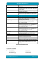
7. Register descriptions
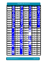
Table 7 lists all of the control and status registers. All of the registers are 8 bit; unused
register bits read back as zeros.
Please note that some registers can be set to values that are illegal and will produce
invalid outputs.
Asserting the RESETn input sets the PT22 registers to their default values.
Register
Offset
Register Name
R/W
$00
Control 1
R/W
$01
Control 2
R/W
$02
Control 3
R/W
$04
PGA_control
R/W
$10
Sync_slice_offs
R/W
PT22 User Manual Revision 0.5
Bit
Value
Description
Control Registers
aCVi Rx control (Output format)
7
Set to ‘1’ to enable the status character overlay, else ‘0’ to
disable the overlay (default).
6:2
Not used
1-0
Value
Output format
00
Not used
01
Y + CbCr (20 bit) + H/V/F (74.25MHz clock)
Default.
10
Not used.
11
Not used.
aCVi Rx control (standard)
7
If ‘0’ the video pattern is displayed, if ‘1’ the video input is
selected (default).
6
If set to ‘1’, the aCVi output free-runs (video black) at the
selected video standard. If set to ‘0’ the output is locked to the
aCVi video input.
5
Not used
4
If ‘0’ (default) the video standard is manually selected using bits
3:0. If ‘1’ the standard is automatically detected from input sync
signals.
3:0
Value
Standard
0000
720p/60 (Default)
0001
720p/50
0010
0011
1000
1080p/30
1001
1080p/25
1010
1011
1100
aCVi Rx control
7:6
Not used
5
Enables automatic colour control (colour gain control) level
adjustment if = ‘1’ (default), else manual adjustment (Register
$40 and $41).
4
Selects the luma low pass filter to be 12MHz (=’1’) or 30MHz
(=’0’ – default).
3
Enables automatic black level adjustment if = ‘1’ (default), else
manual adjustment (Register $40 and $41).
2
Enables automatic luma gain adjustment if = ‘1’ (default), else
manual adjustment (Register $04).
1:0
Bit value
Function
00
VCO control word from phase detector (HPLL
closed - default)
01
VCO control set to minimum
10
VCO control set to maximum
11
VCO control set to 50% (Freerun mode)
7:0
An 8 bit register intended for the control of the analogue front
end programmable gain amplifier. This register is not used
when automatic luma gain control is enabled.
SPG
7:0
Value added to the negative video peak value for slicing the
Page 24 of 28
SingMai Electronics
Register
Offset
Register Name
R/W
Bit
Value
R/W
R/W
R/W
R/W
R/W
7:0
7:0
7:0
7:0
7:0
R/W
3:0
R/W
R/W
7:0
3:0
$1E
$1F
et
FSc_1
FSc_2
FSc_3
FSc_4
Hcount_length_
1
Hcount_length_
2
Hout_start_1
Hout_start_1
$20
$21
Hout_end_1
Hout_end_1
R/W
R/W
7:0
3:0
$22
$23
BP_gate_start_1
BP_gate_start_1
R/W
R/W
7:0
3:0
$24
$25
BP_gate_end_1
BP_gate_end_1
R/W
R/W
7:0
3:0
$2A
$2B
HBlank_start_1
HBlank_start_2
R/W
R/W
7:0
3:0
$2C
$2D
HBlank_end_1
HBlank_end_2
R/W
R/W
7:0
3:0
$2E
R/W
7:0
R/W
2:0
$30
$31
Vcount_length_
1
Vcount_length_
2
Vout_start_1
Vout_start_1
R/W
R/W
7:0
2:0
$32
$33
Vout_end_1
Vout_end_1
R/W
R/W
7:0
2:0
$34
$35
VBlank_start_1
VBlank_start_1
R/W
R/W
7:0
2:0
$36
$37
VBlank_end_1
VBlank_end_1
R/W
R/W
7:0
2:0
$38
$39
SVBlank_start_1
SVBlank_start_1
R/W
R/W
7:0
2:0
$3A
$3B
SVBlank_end_1
SVBlank_end_1
R/W
R/W
7:0
2:0
$40
R/W
7:0
R/W
1:0
$42
$43
Sub_Luma_valu
e_1
Sub_Luma_valu
e_2
Ygain_value_1
Ygain_value_2
R/W
R/W
7:0
1:0
$44
$45
Ugain_value_1
Ugain_value_2
R/W
R/W
7:0
1:0
$46
$47
Vgain_value_1
Vgain_value_2
R/W
R/W
7:0
1:0
$48
ACC
demod_value
ACC
remod_value
R/W
7:0
R/W
7:0
$18
$19
$1A
$1B
$1C
$1D
$2F
$41
$49
Description
sync pulses. Default value = 15610
Subcarrier seed value. 32 bit value = ({FSc_1[7:0], FSc_2[7:0],
FSc_3[7:0], FSc_4[7:0]}).
Default value = 6655D9BAH = 169367737510; Seed value for
58.559489MHz (720p/60Hz).
Horizontal pixel counter length. Should be set to the (number of
pixels/line – 1) for the selected standard. 12 bit word =
({Hcount_length_2[3:0],Hcount_length_1[7:0]}). Default value =
164910 (720p/60Hz).
Start position of horizontal sync output. 12 bit word =
({Hout_start_2[3:0],Hout_start_1[7:0]}). Default value = 10410
(720p/60Hz). 1 LSB = 1/74.25MHz.
End position of horizontal sync output. 12 bit word =
({Hout_end_2[3:0],Hout_end_1[7:0]}). Default value = 16410
(720p/60Hz). 1 LSB = 1/74.25MHz.
Start position of burst gate sample pulse. 12 bit word =
({BP_gate_start_2[3:0],BP_gate_start_1[7:0]}). Default value =
19010 (720p/60Hz). 1 LSB = 1/74.25MHz.
End position of burst gate sample pulse. 12 bit word =
({BP_gate_end_2[3:0],BP_gate_end_1[7:0]}). Default value =
22310 (720p/60Hz). 1 LSB = 1/74.25MHz.
Start position of horizontal blanking pulse. 12 bit word =
({HBlank_start_2[3:0],HBlank_start_1[7:0]}). Default value =
153610 (720p/60Hz). 1 LSB = 1/74.25MHz.
End position of horizontal blanking pulse. 12 bit word =
({HBlank_end_2[3:0],HBlank_end_1[7:0]}). Default value =
153610 (720p/60Hz). 1 LSB = 1/74.25MHz.
Vertical pixel counter length. Should be set to the (number of
lines/frame – 1) for the selected standard. 11 bit word =
({Vcount_length_2[2:0],Vcount_length_1[7:0]}). Default value =
74910 (720p/60Hz).
Start position of vertical sync output. 11 bit word =
({Vout_start_2[2:0],Vout_start_1[7:0]}). Default value = 010
(720p/60Hz). 1 LSB = 1 line.
End position of vertical sync output. 11 bit word =
({Vout_end_2[2:0],Vout_end_1[7:0]}). Default value = 510
(720p/60Hz). 1 LSB = 1 line.
Start position of vertical blanking output. 11 bit word =
({VBlank_start_2[2:0],VBlank_start_1[7:0]}). Default value =
74510 (720p/60Hz). 1 LSB = 1 line.
End position of vertical blanking output. 11 bit word =
({VBlank_end_2[2:0],VBlank_end_1[7:0]}). Default value = 2010
(720p/60Hz). 1 LSB = 1 line.
Start position of short vertical blanking output (burst blanking).
11 bit word = ({SVBlank_start_2[2:0],SVBlank_start_1[7:0]}).
Default value = 74410 (720p/60Hz). 1 LSB = 1 line.
End position of short vertical blanking output (burst blanking).
11 bit word = ({SVBlank_end_2[2:0],SVBlank_end_1[7:0]}).
Default value = 310 (720p/60Hz). 1 LSB = 1 line.
Procamp
Value subtracted from luma output (to remove synchronizing
pulses), if in manual. 10 bit word =
({Sub_Luma_value_2[1:0],Sub_Luma_value_1[7:0]}). Default
value = 46010.
Luma gain control. 10 bit word =
({Ygain_value_2[1:0],Ygain_value_1[7:0]}). Default value =
74610.
Chroma (B-Y) gain control. 10 bit word =
({Ugain_value_2[1:0],Ugain_value_1[7:0]}). Default value =
51210.
Chroma (R-Y) gain control. 10 bit word =
({Ugain_value_2[1:0],Ugain_value_1[7:0]}). Default value =
51210.
ACC gain control value for demodulator (default = 6410).
ACC gain control value for remodulator (default = 6410).
Status and Measurement
PT22 User Manual Revision 0.5
Page 25 of 28
SingMai Electronics
Register
Offset
Register Name
R/W
Bit
Value
R
7:0
R
1:0
R
7:0
R
1:0
Measured back porch value of the filtered luma video (black
level). 10 bit value =
({Video_BP_value_1[7:0],Video_BP_value_2[1:0]}).
R
R
7:0
6:0
Measured peak U burst amplitude value.
Measured input video field rate (field/second).
$56
Negative_peak_
value_1
Negative_peak_
value_2
Video_BP_value
_1
Video_BP_value
_2
Burst_amplitude
Video_Field_Rat
e
Overflow
R
0
$5F
Version No.
R
7:0
$60
Data_Instruction
R/W
$61
$62
Data_Word
Tx_status
R/W
R
$63
Rx_Data_instruc
tion
Rx_Data_word
Rx_status
$50
$51
$52
$53
$54
$55
$64
$65
R
R
R
Description
Measured negative peak value of the filtered luma video (sync
tip value). 10 bit value =
({Negative_peak_value_1[7:0],Negative_peak_value_2[1:0]}).
If this bit high it indicates the video input (ADC) has overflowed
(video gain too high).
SC10 version number.
Data Insertion control
3:0
Instruction word to be transmitted between receiver and
transmitter.
7:0
Data word to be transmitted between receiver and transmitter.
7:1
Not used
0
When the data word is written for transmission (register $4D)
this bit will be set to ‘1’. When the data has been transmitted
(the next occurring line 8) the flag will be reset to ‘0’. New data
should not be written for transmission while this flag is high.
3:0
Received data instruction.
7:0
7:6
5
4
3:2
1
0
Received data word.
Not used.
Calculated instruction word parity.
Received instruction word parity.
Not used.
Calculated data word parity.
Received data word parity.
Table 8 Register description
PT22 User Manual Revision 0.5
Page 26 of 28
SingMai Electronics
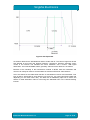
8. PGA amplifier control
For more flexibility the analogue front end can utilize a programmable gain amplifier, allowing
automatic gain control to compensate automatically for cable length.
The evaluation board uses an Analog Devices AD8337 voltage controlled amplifier for this
purpose. The control voltage/gain response for the AD8337 is shown in Figure 6.
Figure 12 AD8337 PGA gain response
As the AD8337 is power from a single supply (+5V) the 0mV gain point is at 2.5V. To provide
a control voltage the PT22 has an 8-bit register (PGA_control) which can be used to control a
pulse width modulator. Example Verilog code for a PWM as used on the evaluation boards is
shown below.
// PWM control of PGA
// Generate 100kHz
always @ (posedge XTAL_clk or negedge RESETn) begin
if (!RESETn) begin
Counter_100k <= 5'd0;
end else if (Counter_100k[4:0] == 5'd26) begin
Counter_100k <= 5'd0;
end else begin
Counter_100k <= Counter_100k + 5'd1;
end
end
// PWM counter
always @ (posedge XTAL_clk or negedge RESETn) begin
if (!RESETn) begin
PWM_counter <= 8'd0;
end else if (Counter_100k[4:0] == 5'd26) begin
PWM_counter <= PWM_counter + 8'd1;
end else begin
PWM_counter <= PWM_counter;
end
PT22 User Manual Revision 0.5
Page 27 of 28
SingMai Electronics
end
always @ (posedge XTAL_clk or negedge RESETn) begin
if (!RESETn) begin
PWM_latch <= 1'b0;
end else if (Counter_100k[4:0] == 5'd26) begin
if (PWM_counter == 8'd0) begin
PWM_latch <= 1'b1;
end else if (PWM_counter == PGA_gain[7:0]) begin
PWM_latch <= 1'b0;
end else begin
PWM_latch <= PWM_latch;
end
end else begin
PWM_latch <= PWM_latch;
end
end
// (Note: PWM Gain control is inverted on DP17
assign Gain = !PWM_latch;
The output (Gain) is a PWM signal whose width is controlled by the PGA_control register.
This output may then be low pass filtered to produce an analogue control voltage.
Figure 13 PWM analogue control.
Figure 7 shows the circuit used on the DP17 evaluation module. The PWM gain signal is first
buffered to move it from the digital powered circuit to the cleaner analogue power. That output
is low pass filtered (R8, C17) to produce an analogue output. This is then buffered by U7, the
output of which drives the AD8337 control voltage input.
PT22 User Manual Revision 0.5
Page 28 of 28