1
ADM-XRC SDK 4.9.3 User Guide (Win32) - ddrsdram_port_v2
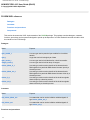
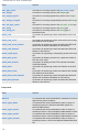
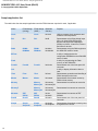
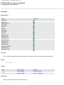
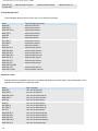
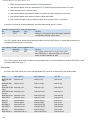
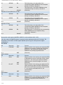
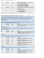
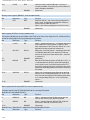
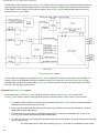
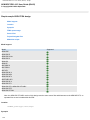
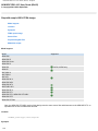
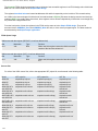
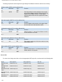
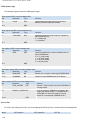
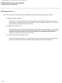
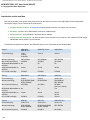
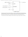
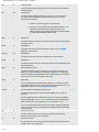
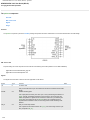
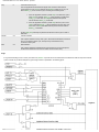
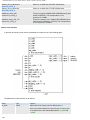
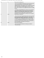
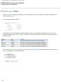
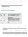
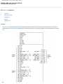
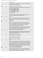
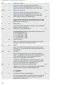
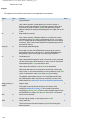
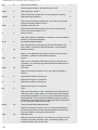
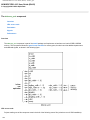
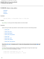
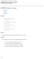
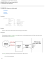
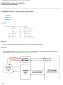
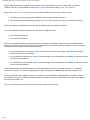
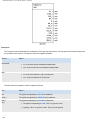
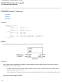
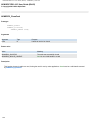
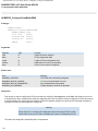
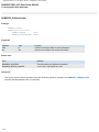
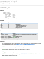
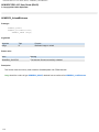
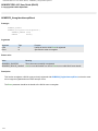
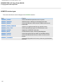
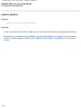
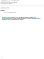
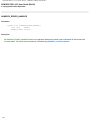
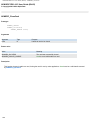
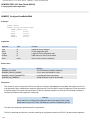
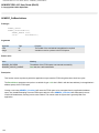
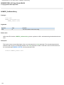
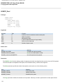
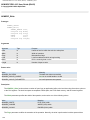
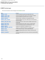
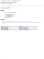
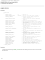
The signals of this interface to and from the memory device(s) are as follows:
Signal
ra
Type
in
Function
Memory device address bus
This bus carries address information to from the memory port
to the memory device(s). For devices with a nontrivial
addressing scheme, this address may be composed of various
fields. These fields are bundled together into the ra bus so
that, for the most part, the user application need not care what
they are.
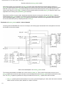
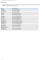
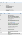
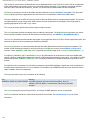
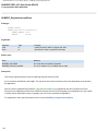
Refer to note 1 for the mapping of the ra bus to device pins.
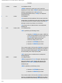
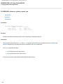
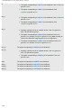
rc
inout
Memory device control bus
This bus carries control signals between the memory port and
the memory device(s), and is composed of various fields.
These signals are bundled together into the rc bus so that, for
the most part, the user application need not care what they
are.
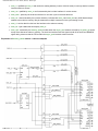
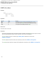
Refer to note 2 for the mapping of the rc bus to device pins.
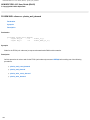
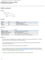
rd
inout
Memory device data bus
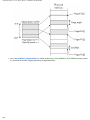
This bus carries data between the memory port and the
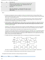
memory device(s). For each command entered via ce, two
words are transferred on rd, which determines the relationship
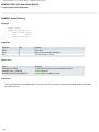
between the rd_width and d_width parameters. Refer to note
3 for details.
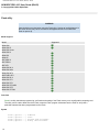
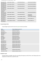
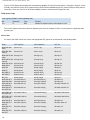
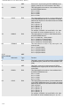
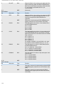
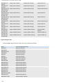
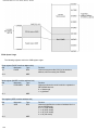
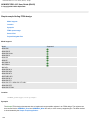
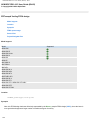
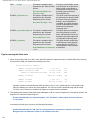
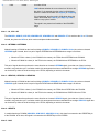
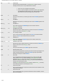
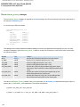
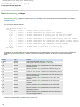
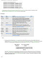
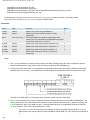
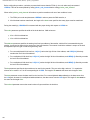
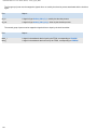
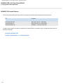
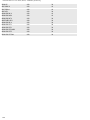
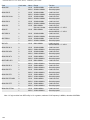
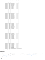
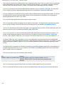
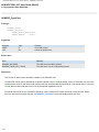
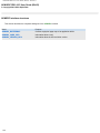
Row / column address selection
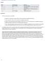
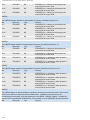
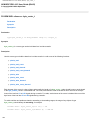
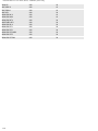
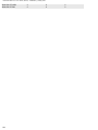
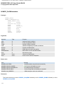
The row and col sideband inputs together determine the number address bits used for row and column addresses, as in the
following table:
row[1:0]
00
00
00
00
01
01
01
01
10
10
10
10
11
11
11
11
331
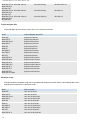
col[1:0]
00
01
10
11
00
01
10
11
00
01
10
11
00
01
10
11
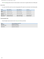
No. of row bits used
12
12
12
12
13
13
13
13
14
14
14
14
15
15
15
15
No. of column bits used
8
9
10
11
9
10
11
12
10
11
12
13
11
12
13
14