1
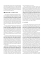
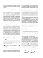
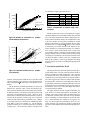
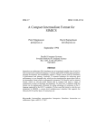
Precise Register Allocation for Irregular Architectures
Timothy Kong and Kent D. Wilken
Dept. of Electrical & Computer Engineering
University of California, Davis
Davis, CA 95616-5294, U.S.A.
fkong,[email protected]
Abstract
This paper proposes a precise approach to register allocation for irregular-register architectures which is based
on 0-1 integer programming (IP). Prior work shows that IP
register allocation is feasible for RISC architectures, which
have uniform registers and register usage. Extensions to the
prior work are proposed that precisely model register irregularities including combined source/destination specifiers,
memory operands, and variations in the cost of register usage. The x86 architecture is selected as a representative
irregular-register architecture for experimental study. An
IP register allocator is built for the x86 architecture within
the Gnu C Compiler (GCC), and is compared experimentally with GCC’s graph-coloring register allocator. Experimental results show that the IP allocator reduces register allocation overhead by 61% compared with the graphcoloring allocator. The results also show that the x86 IP allocator is dramatically faster than the prior RISC IP allocator, because of the smaller number of registers in the x86 architecture and because of the register irregularities. These
results suggest that IP register allocation is well suited for
irregular-register architectures.
1. Introduction
A compiler initially generates code assuming an infinite
number of symbolic registers. In a later compiler phase, the
register allocator maps these symbolic registers to a machine’s real registers. Because the number of real registers is small, not all symbolic registers may get real register assignments, and those symbolic registers must then reside in memory. Spill code is generated to move those symbolic registers to and from memory. The register allocation
problem is to create a register assignment that minimizes the
amount of spill code. Global register allocation analyzes
the entire function at once and attempts to produce an assignment for all symbolic registers in the function. Since
global register allocation is NP-complete [8], most allocators use heuristic techniques to produce a solution.
Traditional allocators perform global register allocation
using a graph coloring approach originally developed by
Chaitin et al. [1]. This approach builds an interference graph whose vertices represent symbolic registers, and
edges connect vertices for symbolic registers that cannot be
assigned the same real register. The graph is then colored
with the same number of colors as there are real registers.
For vertices that did not receive a color, the corresponding
symbolic register is spilled. The allocator relies on heuristics to decide on the order of symbolic registers to spill and
the placement of the spill code.
Goodwin and Wilken proposed a fundamentally new register allocation approach based on integer programming [3].
The Optimal Register Allocation (ORA) approach builds an
integer program (IP) representation of the allocation problem, using integer program variables to represent possible
register allocation actions at each point in the computer program. Each of these actions has an associated cost. An integer program solver solves the IP problem, generating a
solution that minimizes total allocation cost. A set of constraints limits the solver to choose only actions that lead to a
valid allocation. Although global register allocation is NPcomplete, in practice ORA consistently produces optimal allocations in O(n3) time [3].
The basic ORA model described in [3] focuses on processors with uniform register architectures. This paper presents
an IP formulation for irregular register architectures, architectures that place restrictions on register usage. Efficient register allocation for irregular architectures is difficult. However, efficient register allocation is important because many real-world processors have irregular registers.
For many embedded and specialized applications, low hardware cost often drives design decisions, forcing designers
to trade uniformity in register architecture for reduced cost.
Furthermore, the Intel x86 architecture, the most widely
used desktop processor, has an irregular register architecture. Better register allocation for the x86 architecture will
Presented at the 31st International Microarchitecture Conference, December 1998.
c 1998 Association for Computing Machinery, Inc.
Copyright ORA Analysis
Module
Write
ORA Solver
Module
ORA Rewrite
Module
Write
Read
Decision-
Read
Variable
Table
Figure 1. ORA top level modules and data
structures.
potentially benefit a wide range of users.
The rest of this paper is organized as follows. Section 2
gives a brief background on ORA. Section 3 describes features of an irregular register architecture and discusses their
effect on register allocation. Section 4 presents a cost model
suitable for integer programming. Section 5 presents an IP
formulation for irregular register architectures. Section 6
gives experimental results for the x86 architecture, followed
by a conclusion and discussion on future work in Section 7.
2. ORA Background
This section gives a brief overview of the Optimal Register Allocation approach to global register allocation proposed in [3]. The ORA register allocator consists of three
top level modules: the analysis, solver, and rewrite modules, as illustrated in Figure 1. The ORA analysis module
analyzes a function to determine the points in the function
where decisions must be made about various register allocation actions. Each register-allocation decision is a binary
decision: at a specific point in the function a certain register allocation action is either performed (1) or is not performed (0). Register-allocation decisions include whether a
symbolic register should be defined into a specific real register, whether the assignment of a symbolic register to a specific real register should continue, whether a symbolic register should be stored to or loaded from memory, etc. The
ORA analysis module produces a binary decision variable
for each register-allocation decision that must be made, and
records the decision variable and the corresponding register
allocation action in the decision-variable table, as illustrated
in Figure 1.
The ORA solver module uses the information about decision variables, register allocation overheads, and conditions to construct a 0-1 integer program [7], a linear program with the added requirement that each variable must be
assigned an integer solution value that is either 0 or 1. After constructing the 0-1 integer program, an optimal solution
is found using a commercial integer program solver. The
solver determines a value of either 0 or 1 for each decision
variable so the conditions are satisfied and the total register
allocation overhead is optimally reduced. The ORA solver
module then records in the decision-variable table the solution value for each decision variable.
Finally, the ORA rewrite module examines the decisionvariable table to determine each decision variable that was
set to 1 by the solver, and to determine the corresponding
register allocation action. The intermediate instructions are
then rewritten based on the register allocation actions determined by the solver, with each symbolic register replaced by
the assigned real register, and with spill code inserted at the
prescribed locations.
3. Irregular Register Architectures
A register architecture is regular in the programming
model if all registers can be used interchangeably in each instruction without affecting the instruction’s execution time
or the instruction’s size. A register architecture is irregular
if the choice of registers affects instruction execution time,
instruction size, or both. For a register architecture to be regular, all registers must appear homogeneous in structure and
usage. A register structure is homogeneous if all registers
can hold the same data types, and the content of one register
does not interfere with the content of another register. Registers are homogeneous in usage if any register can be used
as an operand whenever a register operand is allowed, and
there is no advantage in choosing one register over another.
Whenever the homogeneity in structure or usage is broken,
the register architecture becomes irregular. This section describes these irregularities and their effect on register allocation.
3.1. Irregularities in Register Structure
A register architecture can become irregular due to irregularities in the structure of the register file. These irregularities limit the generality of the registers. Examples of
these irregularities include the partitioningof the register file
based on data type, and the sharing of bit fields among registers. In partitioningbased on data type, registers are grouped
into sets with each set capable of only holding data of certain types. For example, the Motorola 680x0 processor has
16 general purpose registers, which are divided into sets of
8 “data” and 8 “address” registers [6]. Although all are 32bit registers, values in the data registers are not considered
memory addresses and cannot serve as the base address in
effective address calculations.
In bit field-sharing, the register architecture specifies that
certain registers must have certain bits in common, making the registers physically overlap. Such registers are no
longer independent. Storing a value in one precludes storing
a value in the overlapping registers. An example of bit field
sharing is found in the x86. The 8-bit AL register shares the
same bits as the least significant half of the 16-bit AX register, which in turn shares the same bits as the least significant
half of the 32-bit EAX register [5].
3.2. Irregularities in Register Usage
The second cause of irregularities in the register architecture are irregularities in register usage found in the instruction set. Regarding register usage, an instruction set is regular if all instructions can specify any general purpose register
as source and destination operands, and there is no advantage in selecting one register over another. Although a regular instruction set is easier for the register allocator to handle, in practice sometimes an instruction set is made irregular to reduce instruction size and to allow for all the encoding
needs of the instruction set. This subsection describes these
instruction set irregularities and their effects on register usage.
One way to reduce instruction size is to reduce the number of operand specifiers. The reduction is often accomplished by overloading one operand specifier to specify both
a source operand and a destination operand. This requires
the source and destination operands to be in the same real
register, thus restricting register usage. An example of this
combined source/destination specifier is found in the x86 architecture, which uses the 2-specifier format for most of the
instructions. The instruction ADD EAX,EBX adds the contents of the EAX and EBX registers, and places the result in
EAX.
A second way to reduce instruction size is to specify register operands implicitly, rather than explicitly enumerating
them in the instruction word. This instruction format restricts register usage because the operands must always be
assigned to these implicit registers. The x86 architecture offers many examples of this format: the 32-bit multiply instruction uses the EDX register implicitly to store the most
significant half of the 64-bit product; shift/rotateinstructions
use the CX register implicitly to store the shift/rotate count;
and push/pop instructions use the ESP register implicitly as
the stack pointer.
A third way to reduce instruction size is to offer more
compact forms of frequently used instructions. A compact
form may represent one opcode/register combination, eliminating the need to specify the register operand separately. In
the compact instruction, the register is specified implicitly.
Although the instruction can use all registers as operands,
the compact form reduces code size, and the compiler should
use this form whenever possible. For example, the x86 offers compact versions of many frequently used instructions
involving the AL/AX/EAX register. These compact forms
reduce the instruction size by one byte.
Finally, an instruction set can be made irregular to satisfy the encoding needs of the instruction set. This situation
happens when an encoding pattern that should be used for
an opcode/register combination is used for some other purpose, making the register unavailable for use with the opcode. To amend this deficiency, sometimes a different encoding is given to the opcode/register combination, but the
encoding is larger, resulting in increased instruction size.
The end effect is nonuniform register usage cost. As an example, in the x86, if the base register used in an indexed addressing mode specification is the ESP register, the address
specification requires an extra byte in the instruction. This is
because the encoding that should be used for ESP is used instead to indicate the presence of more bytes in the addressing
mode specification. As a result, irregular instruction encoding causes register usage to appear irregular.
4. Cost Model
A precise register allocator must have an accurate model
of the costs associated with register allocation. An accurate cost model is especially important for irregular architectures, where costs are nonuniform and can arise from many
different sources. In particular, a precise treatment of code
size cost is important because instructions can have variable
size, and the size can depend on the choice of operand registers. Changes in program size in turn affect program execution time because of memory hierarchy effects.
A precise cost model for register allocation can be obtained by dividing the cost of each register allocation action
into its component costs. For each action, there are three
types of costs if the action is taken: (1) the processor cycle
cost, (2) the instruction memory cost, and (3) the data memory cost. The processor cycle cost models the time spent by
the processor executing instructions resulting from the allocation action. For example, a memory load action introduces a load instruction, and the processor cycle cost of the
load action is the number of processor cycles needed to execute the load instruction. The second cost component models the effect of increased instruction size. An allocation action may change the code size of an instruction. A larger
code size increases program execution time because of delays in the memory hierarchy in supplying instructions. In
particular, there will be more instruction cache misses and
more instruction page faults. Finally, the last cost component models the effects of increased data memory access
generated by an allocation action. For example, a store spill
of a 32-bit value accesses the data cache to store the four
bytes of data. Increased data memory access causes more
data cache misses and more data memory page faults.
The cost model can be expressed mathematically for each
integer program decision variable. As described in Section
2, each register allocation action is represented by such a
variable. The cost coefficient for a variable x is given by this
equation:
cost(x) = A cycle(x)
+ B instruction size(x)
+
C data size(x)
(1)
Each term corresponds to the cost component described
above. The factors A, B , and C are the relative weightings
of the cost components. These factors depend on the instruction at which the allocation action applies. For an action at
instruction i, A is the execution count of i and can be obtained through profiling. The factor B gives the additional
memory hierarchy delay caused by each 1-byte increase in
code size at i, and C gives a similar delay due to each 1-byte
increase in data memory access at i. B can be obtained by
profiling instruction cache misses and instructionpage faults
at i. C can be obtained by profiling data cache misses and
data page faults for data accesses originating from spill instructions near i. Some decision variables do not have all
three cost components, and the corresponding cost term is
zero in the cost model.
The main advantage of the model is the ability to account
for diverse allocation costs easily and precisely. As will be
shown in Section 5, unique cycle and memory costs arising
from an irregular register architecture can be calculated precisely using equation (1). Furthermore, the factors A, B ,
and C provide a convenient way to adjust the relative effect
of each cost component. For example, if the goal is to optimize purely for program size, the cycle and the data memory components of the cost can be excluded entirely from
the cost model. This type of optimization is useful, for instance, in embedded applications where the main concern is
to reduce hardware cost, and a smaller program size reduces
hardware cost by requiring less memory for storage.
5. IP Model for Irregular Register Architectures
The IP model for register allocation in [3] can be extended so that register irregularities are precisely modeled.
This section describes the IP model extensions for some
common register irregularities.
5.1. Combined Source/Destination Specier
Various architectures include instructions that use the
same register specifier for one of the source operands and
for the result’s destination. The register allocator is required
to allocate the corresponding source and destination symbolic registers to the same real register. If the source operand
is live after the instruction, the register allocator must copy
that symbolic register into another real register or spill the
symbolic register to memory. In contrast, the three-specifier
format typically found in RISC architectures has no restriction on the assignment of source and destination registers.
Combined source/destination specifiers commonly occur in
architectures that have small instruction sizes (e.g., 16 bits or
less) such as the x86 architecture and the 68000 architecture,
to minimize the number of instruction bits that the register
specifiers consume. This register irregularity also occurs in
some RISC architectures such as the PA-RISC which combine a branch and an arithmetic operation into the same instruction.
For combined source/destination specifiers, register
allocation is problematic for instructions with two source
operands that are commutative, e.g., S1 = S2 + S3.
In the traditional approach to handling the combined
source/destination specifiers for such instructions, a compiler phase prior to register allocation uses a heuristic to
select one of the two source operands to share the combined
specifier. The intermediate representation is then rewritten with a copy inserted that copies the selected source
symbolic register, say S2, to the instruction’s destination
symbolic register, S1. The instruction is then rewritten by
replacing S2 with S1, as illustrated below.
Copy S1 <- S2
S1 = S1 + S3
The register allocator will then allocate the two definitions and use of S1 to the same real register, and may eliminate the copy instruction, if appropriate. This traditional approach to handling combined specifiers is problematic because the choice of which source operand will be combined
with the destination is made outside the context of register
allocation, and thus may often be a poor decision.
The IP allocator can precisely model combined
source/destination specifiers. First, the IP model is extended to allow copies to be inserted. The IP model in [3]
only allows copies to be deleted. For an instruction with
commutative source operands, for each source operand S
a copy insertion transformation is applied that produces
a decision variable xrcopyS for each real register r which
allows S to be copied to r just prior to the instruction, as
shown in Fig. 2. Each xrcopyS variable is given the cost of
the corresponding copy instruction. S can only be copied if
S is live in a register just prior to the instruction. Also, it
is necessary to select at most one of the xrcopyS variables.
These two facts are captured in the following constraint
produced by the copy insertion transformation:
X
r2real regs
xrcopyS X
r2real regs
xrpreS
x
r
preS
use of S
x
x
r
loadS
x
r
copyS
x
r
use-endS
r
use-contS
Figure 2. Potential copy before use of symbolic register S.
where xrpreS is the variable produced by a preceding transformation which represents whether S is allocated (not allocated) to r just prior to the instruction [3].
Also at an instruction with commutative source
operands, a condition is added that enforces the combined
source/destination specifier requirement. For instruction
S1 = S2 op S3, S1 can be allocated to real register r
only if S2 is allocated to r just prior to the instruction and
the allocation of S2 to r ends at the instruction or S3 is
allocated to r just prior to the instruction and the allocation
of S3 to r ends at the instruction. This fact is captured by
applying a combined specifier transformation which for
each r produces the constraint:
xrdefS 1 xruse,endS 2 + xruse,endS 3
where the xruse,endS is 1 if S is allocated to r at the instruction and the allocation ends at the instruction [3]. Note that
the left-hand side is less than or equal rather than equal because it is possible for the allocation of both source operands
to end at the instruction, one ending in real register rx and
the other ending in real register ry. Because S1 is only derx
fined into one register, either xrx
defS 1 or xdefS 1 will be zero,
which is less than the corresponding right-hand side.
Although the proposed IP model will optimally insert copies prior to instructions with commutative source
operands, the problem of optimal copy insertion at any program location is beyond the scope of this paper (this problem
will be considered in a forthcoming paper.) Thus under the
assumption that the allocator can insert copies, the proposed
IP model for irregular register architectures is precise but it
is not optimal.
5.2. Memory Operands
In [3] Goodwin and Wilken consider one aspect of register irregularity, non-load/store architectures which directly
use memory operands. The IP model in [3] applies to instructions that allow a separate memory specifier for each
memory source operand and/or each memory destination.
However various non-load store architectures include instructions that use combined source/destination memory
specifiers. Here we describe an extension to the IP model
for combined source/destination memory specifiers. This
model makes optimal use of combined source/destination
memory specifiers under the traditional register-allocation
assumption that each symbolic register has a unique spill location. With this assumption, the source/destination memory operands that have a combined specifier must be the
same symbolic register.
At an instruction that allows a combined
source/destination memory specifier and that has symbolic
register S as a source operand and as a destination, a combined memory specifier transformation is applied that produces a decision variable xcombined,mem,use=defS which
represents the use of S from memory and the definition of S
to memory. The variable xcombined,mem,use=defS is given
a cost that represents the overhead that occurs for reading
from and writing to memory, and the overhead for code size
increase caused by the memory specifier. The combined
memory specifier can only be used if S is in memory just
prior to the instruction. Thus the transformation produces
the condition xcombined,mem,use=defS xmem
preS , where
xmem
is
the
variable
produced
by
a
preceding
transpreS
formation which represents whether S is allocated (not
allocated) to memory just prior to the instruction. The
variable xcombined,mem,use=defS is included in the must
allocate condition [3] for the use, which ensures that S is
either allocated to a register or to memory at the use. The
variable xcombined,mem,use=defS is also included in the
must allocate condition for the definition. The variable
xcombined,mem,use=defS can be used in combination with
the xmemory,useS and xmemory,defS variables described
in [3], so that the definition and use of S are optimally
allocated both to registers, to a register and to memory
using a separate memory specifier, or both to memory using
a combined specifier.
5.3. Overlapping Registers
Some architectures have registers that physically overlap. Storing a value in one register necessarily means that
a value cannot be stored in the overlapped register. The x86
architecture is such an example. The x86 architecture defines certain registers as bit fields of larger-sized registers.
In particular, 16-bit registers are defined as the least significant 16 bits of 32-bit general purpose registers, and 8-bit registers are defined as the two least significant 8-bit fields of
the EAX, EBX, ECX, and EDX registers. Fig. 3 shows the
mapping for the 32-bit EAX register and the registers con-
EAX
at another program location only S1 and S3 are live. The
generalized single-symbolic constraint becomes:
AX
AH
AL
Figure 3. Mapping between EAX, AX, AH, and
AL registers.
tained within EAX. For register allocation, bit field sharing
implies that the registers involved can together hold at most
one value at a time.
Register allocation for registers with common bit fields
can be modeled as follows. All real registers that share a
common bit field are grouped into a set. Each register in a
set is allocated as a distinct, individual register, with the restriction that at most one register in the set can be allocated
to any symbolic register at any given program location. This
restriction enforces the fact that there is only one underlying
bit field in the register set, and this bit field is in use when
any register in the set is in use. A register can be a member of more than one set. For example, EAX is in the sets
fEAX, AX, ALg and fEAX, AX, AHg. EAX is in the first
set because it shares the least significant 8 bits with AX and
AL, and it is in the second set because it shares the next least
significant 8 bits with AX and AH.
To model bit-field sharing between registers, a generalized single-symbolic constraint [3] is generated after each
define that involves any register in a register set. A singlesymbolic constraint limits to one the number of symbolic
registers that a real register can hold. A generalized singlesymbolic constraint encompasses all registers in a register
set, and limits the total number of symbolic registers that all
registers in the set can hold together to one. It is possible that
not all registers in a set are needed for register allocation because there are no live symbolic registers of the corresponding size. At these program locations, the unneeded registers
in the set are excluded from the generalized single-symbolic
constraint.
As an example, consider symbolic registers S1, S2, and
S3, where S1 is 32-bit, S2 is 16-bit, and S3 is 8-bit. The
following is the generalized single-symbolic constraint for
real register EAX at a program location where S1, S2, and
S3 are all live:
AX
AL
xEAX
S 1 + xS 2 + xS 3 1
AX
AH
xEAX
S 1 + xS 2 + xS 3 1
xEAX
S1
S 1 is the 0-1 decision variable that indicates whether
AL . The
is assigned to EAX, and similarly for xAX
and
x
S2
S3
first constraint applies to the register set fEAX, AX, ALg,
and the second applies to fEAX, AX, AHg. Now assume
AL
xEAX
S 1 + xS 3 1
AH
xEAX
S 1 + xS 3 1
The xAX
S 2 term is missing because the AX register is not
needed for register allocation.
5.4. Instruction Encoding Irregularities
In some architectures, the instruction size can vary depending on the register specified in the instruction. For certain instructions, using a specific register as an operand will
result in smaller code size, while others will cause code size
to increase. Furthermore, not all registers may appear in all
addressing modes. These instruction encoding irregularities
can be modeled precisely in the IP allocator, leading to an
allocation that takes into account these diverse effects. This
subsection presents cases in the x86 architecture.
5.4.1. Short Opcodes with AL/AX/EAX Registers
The x86 instruction set allows smaller code size for certain
instructions if the register operand is AL, AX, or EAX. In
particular, the instruction size is shorter by one byte if the
instruction uses the AL/AX/EAX register and an immediate operand. The shorter instruction size is available for
these commonly used instructions: ADC, ADD, AND, CMP,
OR, SUB, TEST, XCHG, and XOR. For this reason, significant code size reduction is possible if the register allocator
assigns the AL/AX/EAX register to these instructions whenever these instructions appear with an immediate operand.
The shorter instruction is modeled in the IP allocator by a
reduced cost on the decision variables corresponding to the
allocation of symbolic registers to the AL/AX/EAX register.
Specifically, for an instruction that uses symbolic register A,
if the instruction has a shorter size when the EAX register is
allocated to A, then the decision variable that describes the
allocation of EAX to A would have a lower memory cost:
instruction size(xEAX
A )=M
,1
where M is the memory cost of allocating A to any real register besides EAX.
5.4.2. Long Addressing Mode Specifications
The x86 uses an additional one or two bytes after the instruction opcode to specify the addressing mode and the registers
used in the effective address calculation. Six of the eight x86
general purpose registers can participate in these addressing
modes. The other two, ESP and EBP, can participate with
the following penalties.
The ESP register, which is the architectural stack pointer
register, requires two bytes in the addressing mode specification when used as a base address register. Specifying [ESP] requires two bytes, and dsp8[ESP] requires
2 bytes plus an additional byte for the displacement dsp8.
In contrast, using any other general purpose register as the
base register requires only one byte. Hence, there is a one
byte penalty for using ESP as the base register.
The EBP register, which is the frame pointer register, requires two bytes in the addressing mode specification when
used as an index register without an offset. The addressing
mode [EBP] requires two bytes. In contrast, this addressing mode requires only one byte if it involves any other general purpose register. Hence, there is a one byte penalty for
using EBP in this manner.
The additional cost of using ESP and EBP in address
mode specification can be represented in the IP model as follows. To model the one byte increase, a decision variable is
generated to represent the use of a symbolic register from
each of these registers. The variable has a higher relative
cost, and the variable can be set to 1 only if the real register is allocated to the symbolic register at that program location. The variable is entered into the must-allocate constraint, which ensures that at least one real register is allocated to the symbolic register at that program location.
Fig. 4 shows an example. The symbolic register A is used
to indirectly address memory. If A resides in EBP and is used
from EBP, then the instruction would incur one extra byte
in the address specification. The variable xEBP
useA models this
use with a higher memory cost:
EBP
xEBP
useA xpreA
instruction size(xEBP
useA ) = M + 1
M is the memory cost of using the symbolic register from
any real register besides EBP. xEBP
preA is set to 1 if EBP is allocated to A just before the instruction. xEBP
useA is set to 1 if A
resides in EBP and is used from EBP. The condition allows
for the possibility of allocating EBP to A (xEBP
preA = 1) without using the value of A from EBP (xEBP
useA = 0). This can
occur if the solver finds it beneficial to put multiple copies
of A into different real registers. In this case, the use of A
with the higher cost will not be chosen, i.e., xEBP
useA would be
0. The must-allocate constraint for A is as follows:
xEBP
useA +
X
xrpreA 1
r2real regs; r6=EBP
EBP
xuseA is entered into the must-allocate constraint instead of
xEBP
preA to correctly account for the higher memory cost.
5.4.3. Exclusion from Addressing Mode
The ESP register cannot be used in all addressing modes.
Specifically, while it can serve as the index register, it can
symbolic register networks for A
...
EAX
ESP
EBP
x
EBP
preA
x
EAX
preA
x
ESP
preA
... = ...,[A]
Figure 4. Higher cost of addressing mode
specification using EBP.
ESP
x
symbolic register networks for A
EAX
...
EBP
ESP
preA
x
EAX
preA
x
EBP
preA
... = ...,[2 * A]
Figure 5. ESP cannot be used in scaled-index
addressing mode.
not be scaled by the constants 2, 4, or 8, e.g., cannot have [2
* ESP]. In contrast, all other general purpose registers can
be used as index registers with scaling by these constants.
The fact that ESP cannot be used in the scaled-indexed
addressing mode can be modeled as follows. At an instruction that uses symbolic register A for such an addressing
mode, the IP variable corresponding to the allocation of A
to ESP is excluded from the must-allocate constraint for A.
Thus, A must reside in some real register besides ESP. For
the example in Fig. 5, the must-allocate constraint is as follows:
X
r2real regs; r6=ESP
xrpreA 1
The constraint forces the IP solver to put A in another real
register besides ESP.
5.5. Predened Memory Symbolic Registers
A predefined memory value is a value that exists in memory at function entry. For symbolic registers that are defined by the loading of a predefined memory value, it may
be possible to coalesce the home memory locations of the
live range
symbolic
live range memX register
network of A
X A
original define
of A, can
be removed
X
A
spill load of A
define of A
A = load(memX)
A = load(memX)
...
A = load(memX)
portion
that
can be
deleted
... = A op ...
A: symbolic register
X: predefined memory value
memX: home location of X in memory
Figure 6. Removing symbolic register network segment for a predefined memory symbolic register.
symbolic register and the predefined memory value. If coalescing is performed, the symbolic register becomes a predefined memory symbolic register. Fig. 6 shows an example
of a predefined memory value X and a predefined memory
symbolic register A that is associated with X. The symbolic
register A shares the same memory location as X, which is
labeled memX.
The coalescing of home memory locations has several
benefits. First, the coalescing allows the removal of the load
instruction that originally defines the symbolic register. Because the symbolic register now has the same home memory location as the predefined memory value, the symbolic
register is considered to exist initially in memory, and no
instruction is required to define it. Second, since the symbolic register and the predefined memory value share the
same memory location, the program’s runtime memory requirement is reduced. Third, the IP formulation is simplified. For a predefined memory symbolic register, the symbolic register network from the original define instruction to
the symbolic register’s first use can be removed, as shown
in Fig. 6. In this region, the symbolic register’s value exists
only in memory, making the symbolic register network unnecessary. The symbolic register network begins just before
the symbolic register’s first use, where the symbolic register
may be loaded into a real register.
A symbolic register becomes a predefined memory symbolic register through association with a predefined memory
value. A symbolic register can be associated with a predefined memory value if (1) the symbolic register is defined by
a load instruction that loads the predefined memory value,
(2) the live ranges of the symbolic register and the predefined memory value do not interfere, and (3) the predefined
memory value is not aliased. The first condition asserts that
memX
X A
...
X
A = A op ...
spill store of A
store A
...
last use of X,
wrong value loaded
... = load(memX)
A
A: symbolic register
X: predefined memory value
memX: home location of X in memory
Figure 7. Overwriting of predefined memory
value by symbolic register.
the initial value of the symbolic register and the predefined
memory value are identical. The only effect of the defining instruction is to transfer the value from memory to a real
register. When the instruction is deleted, the value of the
symbolic register is unchanged, but the value now resides
in memory instead of in a real register.
The second condition prevents the overwriting of either’s
memory value by the other. It is easy to show that this condition is necessary using counter examples. Fig. 7 shows
the symbolic register A and the predefined memory value X
sharing the same home memory location, but the live ranges
of A and X intersect. The figure shows A spilling within the
live range of X, overwriting the value of X in memory. When
X is later used, the wrong value of X is loaded. Similarly,
changing the predefined memory value may alter the value
of a symbolic register. Fig. 8 shows the same symbolic register A and the same predefined memory value X. X is modified within the live range of A. When A is later loaded from
memory, the wrong value of A is returned.
The third condition requires that the predefined memory
value is not aliased. Aliasing allows the predefined memory value to be modified or used beyond the program location where the predefined memory value is explicitly loaded.
Consider the following example, where X is a predefined
memory value residing in memory location memX:
...
A = load (memX)
call foo (memX)
...
The subroutine foo is invoked with the address of memX.
Since the subroutine can potentially modify X, X is aliased,
live range memX
X A
define of A
A = load(memX)
...
X
A = A op ...
spill store of A
store A
...
X is modified
A
memX = ...
number of processor cycles to execute as on the Pentium
[5]. Table 1 gives the cycle and memory cost for instructions used by the register allocator. Cycle cost in the table
is the number of processor cycles required to execution the
instruction. Memory cost is the instruction’s size in bytes.
instruction
load
store
rematerialization
copy
cycle cost
1
1
1
1
memory cost
3
3
3
2
...
last use of X
... = memX
Table 1. Spill code cost.
X
...
spill load of A
wrong value loaded A = load(memX)
... = A
last use of A
A: symbolic register
X: predefined memory value
memX: home location of X in memory
Figure 8. Overwriting of symbolic register by
changing the predefined memory value.
and A cannot be assigned the same memory home location
as X.
6. Experimental Results
An IP allocator for the x86 architecture has been built inside the Gnu C compiler [9]. The x86 architecture was chosen because it includes a large variety of register irregularities and because of its widespread use. The integer program
generated by the IP allocator is sent to a CPLEX 6.0 integer program solver [4]. The solver runs on a HP 9000/780
workstation with a 160MHz PA-8000 processor and 256MB
of main memory. The SPEC92 [2] integer benchmarks are
used as test inputs. The benchmarks consist of six programs:
compress, eqntott, xlisp, sc, espresso, and cc1. For each
function in a benchmark, a maximum solver time limit of
1024 seconds is allowed.
The experiment assumes a simplified version of the cost
model described in Section 4. In the simplified model, the
factor A is obtained through instruction execution profiling
as described. The factors B and C are estimated. B is set to
1000 to model the effect of increased code size. Specifically,
it takes on the order of 1000 processor cycles to read in a
byte of program code from disk storage. C is set to zero.
The experiment assumes a Pentium implementation of
the x86 architecture. Each instruction requires the same
Table 2 shows the number of functions solved. The column total shows the number of functions in the benchmark.
Of these functions, attempted is the number of functions that
are passed to the IP allocator for allocation. Some functions
are not passed to the IP allocator because they operate on
64-bit integer values, which the IP allocator currently does
not handle. The solved column lists the number of function
for which the IP solver is able to generate a feasible allocation. The optimal column lists the number of functions for
which the IP solver generated an optimal solution. Although
the IP solution is optimal relative to the model, the allocation solution is not optimal because the present IP model
does not insert copies optimally, as discussed in Section 5.1.
Of the functions that are attempted by the IP allocator, the
IP solver generated a feasible allocation for 98.1% of them.
The solver was able to generate optimal solutions for 97.6%
of the functions it attempted, within the time limit of 1024
seconds.
SPECint92
Benchmark
compress
eqntott
xlisp
sc
espresso
cc1
Total
Total
16
62
357
154
361
1450
2400
Functions
Attempted Solved
16
16
62
62
357
357
146
146
361
361
1421
1412
2363
2354
Optimal
16
62
357
142
360
1405
2342
Table 2. Number of functions solved with a
solver time limit of 1024 seconds.
Fig. 9 shows the size of the IP program against the number of GCC intermediate instructions. Constraints growth
rate is only slightly higher than linear relative to the number
of intermediate instructions. Fig. 10 shows optimal solution
time against the number of constraints. The optimal solution time is the time the solver takes to produce an optimal
Integer Program Constraints
overhead due to register allocation by 61%.
100000
10000
1000
solved optimally
solved non-optimally
not solved
100
10
1
10
100
Intermediate Instructions
1000
Optimal Solution Time (secs.)
Figure 9. Number of constraints vs. number
of intermediate instructions.
1000.00
100.00
10.00
n
3
1.00
0.10
0.01
100
n
2
1000
10000
Integer Program Constraints
Overhead Type
Spill Load
Spill Store
Rematerialization
Copy
Total
IP
373M
317M
144M
-331M
503M
GCC
902M
565M
-5.0M
-53M
1410M
IP / GCC
0.41
0.56
-29
6.3
0.36
Table 3. Components of dynamic spill code
overhead.
The IP solution times for the x86 architecture is significant faster than the times for the RISC architecture presented
in [3]. The x86 IP model has only about a quarter of the constraints found in the RISC model. The simplification is due
to the fewer number of real registers available for register
allocation; the x86 has 6, whereas the RISC has 24. Since
IP solution time is roughly O(n2:5) relative to the number
of constraints, a four times decrease in the number of constraints translates to a solution time speedup of 32. Furthermore, a newer version of the CPLEX solver is used, yielding a speedup of about 2, and a faster solver machine is used,
giving a speedup of about 3. Total IP solution time speedup
is roughly 192. Furthermore, the irregular cost nature of the
x86 IP model helps to reduce solver time. Irregular costs
break up the symmetry of the integer program, decreasing
the time spent by the solver in searching through equivalent
solutions.
7. Conclusion and Future Work
Figure 10. Optimal solution time vs. number
of constraints.
solution, for those functions that the solver was able to find
optimal solutions. The growth rate of the optimal solution
time is roughly O(n2:5) with respect to the number of constraints.
The IP allocator produced significantly less spill code
than the GCC allocator. Table 3 shows the amount of dynamic spill intermediate instructions produced by both the
IP allocator and GCC. The IP allocator produced fewer load
and stores, and eliminated more copies. However, GCC
deleted more rematerialization instructions than it inserted.
Overall, the IP allocator produced only 36% of the total
amount of spill instructions as produced by GCC. Changes
in execution time can be calculated by substituting values
from Tables 1 and 3 into equation (1). The IP allocator
produced 551M cycles of overhead, while GCC produced
1410M cycles. The IP allocator reduces execution time
The paper described an IP-based register allocator for irregular architectures. Previous work showed that an IP allocator is feasible for a RISC architecture, where registers
are uniform and can be treated identically. The work presented here shows the IP approach for an irregular architecture, where registers have distinctive features and should be
treated separately. Furthermore, the IP approach is shown to
be particularly well suited to irregular architectures, because
individual costs can be modeled precisely and accurately in
the IP model. These costs, on the other hand, make allocation using heuristics difficult.
The paper discussed several irregular architecture features, but there are others that remain to be modeled. For
example, instruction selection can be integrated into register allocation to further reduce spill code. The IP allocator
can be extended to use other instructions, such as the x86’s
XCHG, which exchanges the contents of two registers. Finally, the current paper does not address the issue of optimally inserting copy instructions, which are important in
processors with combined source/destination operand specifiers.
Work is under way to port the IP allocator to a commercial x86 compiler. The resulting setup will allow a comparison between the IP allocator and an aggressive industrial allocator. The result will be reported in a future paper.
Acknowledgements
This research was sponsored by Microsoft Research and
by the University of California under the UC MICRO program.
References
[1] G. Chaitin, M. Auslander, A. Chandra, J. Cocke, M. Hopkins,
and P. Markstein. Register allocation via coloring. Computer
Languages, 6:47–57, 1981.
[2] K. Dixit. New CPU benchmark suites from SPEC. In Digest of
Papers Compcon, Spring 1992, pages 305–310. IEEE, 1992.
[3] D. Goodwin and K. Wilken. Optimal and near-optimal global
register allocation using 0-1 integer programming. Software–
Practice and Experience, 26(8):929–965, 1996.
[4] ILOG, Inc., CPLEX Division. CPLEX 6.0 Documentation
Supplement, 1998.
[5] Intel. Pentium ProcessorFamily Developer’s Manual, Volume
3: Architecture and Programming Manual. Intel Corporation,
1995.
[6] Motorola. MC68020 32-Bit Microprocessor User’s Manual.
Prentice-Hall, Inc., 1985.
[7] G. Nemhauser and L. Wolsey. Integer and Combinatorial Optimization. John Wiley & Sons, 1988.
[8] R. Sethi. Complete register allocation problems. SIAM Journal on Computing, 4(3):226–248, September 1975.
[9] R. Stallman. Using and Porting GNU CC. Free Software
Foundation, Inc., 1995.