1
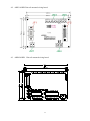
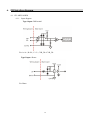
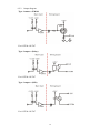
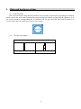
LSI3101/3101A Quadrature Encoder/Linear Scale Counter Card User's Manual (V1.3) 健昇科技股份有限公司 JS AUTOMATION CORP. 新北市汐止區中興路 100 號 6 樓 6F., No.100, Zhongxing Rd., Xizhi Dist., New Taipei City, Taiwan TEL:+886-2-2647-6936 FAX:+886-2-2647-6940 http://www.automation.com.tw http://www.automation-js.com/ E-mail:[email protected] Correction record Version Record 1.0 firmware version 1.0 up 1.1 add LSI3101A 1.2 1.3 add LSI3101 V1.2 SV1.1 diagram add JP1 description Modify 2. Feature-Delete Software key function 1 Contents 1. Forward ............................................................................................................................................... 4 2. Features ............................................................................................................................................... 5 2.1 Main card .................................................................................................................................... 5 2.2 Din rail mounted wiring board .................................................................................................... 6 Specifications ...................................................................................................................................... 7 3.1 LSI3101/3101A Main card.......................................................................................................... 7 3.2 Din rail mounted wiring board .................................................................................................... 9 Layout and dimensions ..................................................................................................................... 10 4.1 LSI3101/3101A Main card........................................................................................................ 10 4.2 ADP3101DIN Din rail mounted wiring board .......................................................................... 11 4.3 ADP9201DIN Din rail mounted wiring board ....................................................................... 11 3. 4. 4.4 JS51053 for ADP9201_JM1 20PM Din rail mounted dummy wiring board ........................... 12 5. 6. 7. Pin definitions for main card connectors .......................................................................................... 13 5.1 JF1 pin definitions ..................................................................................................................... 13 5.2 ADP9201_JM1 pin definitions ................................................................................................. 13 I/O Interface diagram ........................................................................................................................ 14 6.1 JF1 ADP3101DIN ..................................................................................................................... 14 6.2 ADP9201_JM1 ADP9201DIN .................................................................................................. 15 Using wiring board ........................................................................................................................... 17 7.1 ADP3101DIN wiring board ...................................................................................................... 17 7.2 ADP9201DIN wiring board ...................................................................................................... 18 8. Main card hardware settings ............................................................................................................. 19 8.1 Card ID setting .......................................................................................................................... 19 8.2 JP1 Hot reset jumper ................................................................................................................. 19 9. Applications ...................................................................................................................................... 20 10. Ordering information ........................................................................................................................ 21 2 Notes on hardware installation Please follow step by step as you are installing the control cards. 1. Be sure your system is power off. 2. Be sure your external power supply for the wiring board is power off. 3. Plug your control card in slot, and make sure the golden fingers are put in right contacts. 4. Fasten the screw to fix the card. 5. Connect the cable between the card and wiring board. 6. Connect the external power supply for the wiring board. 7. Recheck everything is OK before system power on. 8. External power on. Congratulation! You have it For more detail of step by step installation guide, please refer the file “installation.pdf “ on the CD come with the product or register as a member of our user’s club at: http://automation.com.tw/ to download the complementary documents. 3 1. Forward Thank you for your selection of PCI bus LSI3101/3101A quadrature encoder/linear scale interface card. In the field of automation, encoder and linear scale as feedback or measuring element is common used in the microprocessor control system. But for the versatile application in PC ba sed control, only a few selections you can make. With the state of the art technology of FPGA chip, photo/magnetic coupler isolation and experienced functions such as external triggered clear counter, auto increment compare equal or FIFO pre-programmed compare equal output to trigger external devices, low cost and high performance makes this card a better choice to use in the servo control feedback and other applications which are concerning quadrature encoder or linear scale. Other encoder/linear scale interface card: LSI3104 4 axes quadrature encoder/linear scale counter card (PCI bus) LSI3123L low cost 3 axes quadrature encoder/linear scale counter card (no touch probe trigger latch function) (PCI bus) LSI3123 3 axes quadrature encoder/linear scale counter card (PCI bus) LSI3123A 3 axes quadrature encoder/linear scale counter card with fast coordinate rebuild function (PCI bus) LSI3134 4 axes quadrature encoder/linear scale counter card with 1 axis FIFO compare mode (PCI bus) LSI3144 4 axes quadrature encoder/linear scale counter card with 2 axes FIFO compare mode (PCI bus) LSI5123 3 axes quadrature encoder counter interface (USB) LSI5123L 3 axes quadrature encoder counter interface (no external trigger latch mode) (USB) LSI5123A 3 axes quadrature encoder counter interface (High noise immunity , Accurite linear scale absolute coordinate mode) (USB) Any comment is welcome, please visit our website http://www.automation.com.tw/ http://www.automation-js.com/ for the up to date information. 4 2. Features 2.1 Main card 2.1.1 PCI plug and play function with card ID for 16 identical cards 2.1.2 High noise immunity with magnetic/photo-coupler isolation 2.1.3 Supports DIN rail mounted wiring board 2.1.4 32bit timer based on 1us time base DIO block 2.1.5 8 photo isolated digital input 2.1.6 8 photo isolated digital output 2.1.7 Software debounce for digital input 2.1.8 Software programmable I/O polarity 2.1.9 Interrupt from IN00~IN07 Quadrature counter block 2.1.10 32-bit counter 2.1.11 16 MHz max. Quadrature input rate (LSI3101A) 8 MHz max. Quadrature input rate (LSI3101) 2.1.12 Quadrature, pulse/direction and up/down counting 2.1.13 Programmable multiple rate at X1, X2, X4 2.1.14 Software debounce for input signals 2.1.15 Multiple counter reset (homing) modes 2.1.16 Differential or single-end input signal 2.1.17 Single or auto increment compare mode 2.1.18 FIFO compare mode 2.1.19 Output gated control 2.1.20 Programmable duration for Compare output 2.1.21 Interrupt on compare equal, FIFO near end 5 2.2 Din rail mounted wiring board 2.2.1 LED display for digital I/O 2.2.2 Application specific connectors 2.2.3 Step down s.p.s. for external 5V 6 3. Specifications 3.1 LSI3101/3101A Main card Counter block 3.1.1 Number of axes: 1 3.1.2 Input : 5 magnetic isolation (A,B,Z,CLEAR,HOME input), TTL level 3.1.3 Output : 1 magnetic isolation (compare out), TTL level 3.1.4 Maximum quadrature input frequency : 8MHz x 4 (LSI3101) 16MHz x 4(LSI3101A) 3.1.5 Encoder Type: Single-end or differential (with ADP3101 DIN wiring board) 3.1.6 Input software debounce: for LSI3101: 512k, 1M, 2M, 4M, 8M (programmable) for LSI3101A:512k, 1M, 2M, 4M, 8M,10M,16M (programmable) 3.1.7 Input multiple rate: X1, X2, X4 programmable (quadrature signal only) 3.1.8 Counter length : 32 Bits 3.1.9 Counter Mode : (QUADRATURE),(CLOCK/DIRECTION), (UP CLOCK/ DOWN CLOCK) 3.1.10 Sample clock frequency: 33MHz 3.1.11 PCI data width : 32 Bits 3.1.12 FIFO depth : 1023 3.1.13 Compare out one shot duration : 1 ~ 65535 us Digital block 3.1.14 Input : 8 photo-isolated , 3.1.15 ON state : 2.8Vdc(max) 4.5mA(min) 3.1.16 OFF state : 8Vdc(min) 3mA(max) 3.1.17 Switching speed : 10KHz max. (limit by photo coupler speed and debounce filter ) 3.1.18 Software debounce: 100Hz, 200Hz, 1KHZ,. No debounce (programmable) 3.1.19 Interrupt at IN00 ~ IN07 7 3.1.20 Output : 8 photo-isolated, 3.1.21 Output range : Open collector 0 ~ 45 Vdc (on card) 3.1.22 Output rating : (With ADP3101 DIN wiring board) 3A @250Vac, 30Vdc (Relay) 1A @ 24Vdc (PMOS) 2A @ 240Vac (SSR) 3.1.23 Sink current : 500mA(peak) per channel (on card) 3.1.24 Switching speed : 20KHz(max)(MOS out only) Timer block 3.1.25 Timer time base: 1us 3.1.26 Timer/counter length:32 bit General 3.1.27 Card ID : 4 bits, 16 position 3.1.28 Insulation resistance : 1000Mohm (min) at 1000Vdc 3.1.29 Isolation voltage : 2500Vac 1 min 3.1.30 Connector : one 20 pin SCSI-II female connector one 20 pin flat cable connector 3.1.31 Operation temperature : 0 to +70 degree C 3.1.32 Storage temperature : -20 to +80 degree C 3.1.33 Operation humidity : 5-95% RH, non-condensing 3.1.34 Dimension : 130(W) * 102(H)mm , 5.2(W) * 4.1(H)in 8 3.2 Din rail mounted wiring board ADP3101DIN DIN rail mounted wiring board 3.2.1 External Supply : DC 24V ± 4V 3.2.2 Single end/ differential signal : jumper select 3.2.3 Connector: SCSI-II 20P cable to connect main and wiring board 3.2.4 On board build-in s.p.s. : DC+5V 500mA (max) 3.2.5 Dimension : 86(W) * 103(L) *45(H)mm; 3.4(W)*4.1(L)*1.8(H)in ADP9201DIN DIN rail mounted wiring board 3.2.6 External Supply : DC 24V ± 4V 3.2.7 Input : 8 with LED indicator 3.2.8 Output : ADP9201DIN(R) : 8 relays (3A @250Vac, 3A @30Vdc) with LED indicator ADP9201DIN(S) : 8 SSR (2A @240Vac) with LED indicator ADP9201DIN(P) : 8 PMOS (Source 1A @24Vdc) with LED indicator 3.2.9 Connector: One 20-pin male flat-cable connector 3.2.10 Operation Temperature: 0 to +70 degree C 3.2.11 Operation Humidity: RH5~95%, non-condensing 3.2.12 Dimension: ADP9201DIN(R) / (P) : 86(W) * 103(L) *45(H)mm; 3.4(W)*4.1(L)*1.8(H)in ADP9201DIN(S) : 86(W) * 103(L) *50(H)mm 3.4(W)*4.1(L)*2.0(H)in JS51053 20PM Din rail mounted dummy wiring board 3.2.13 Dimension: 86(W)*79(L)*52(H)mm, 3.4(W)*3.2(L)*2.1(H)in 9 4. Layout and dimensions 4.1 LSI3101/3101A Main card LSI3101 V1.0 SV1.0 LSI3101 V1.2 SV1.1 Note: Both the two versions are software and hardware compatible 10 4.2 ADP3101DIN Din rail mounted wiring board 4.3 ADP9201DIN Din rail mounted wiring board 11 4.4 JS51053 for ADP9201_JM1 20PM Din rail mounted dummy wiring board 12 5. Pin definitions for main card connectors 5.1 JF1 pin definitions PIN DESCRIPTIONS 1 +5Vin: 5V input from wiring board 2 +5Vin: 5V input from wiring board 3 A+: phase A+ input 4 B+: phase B+ input 5 Z+: phase Z+ input 6 CLR_IN+: clear+ input 7 NC 8 HOME: home limit switch input 9 NC PIN DESCRIPTIONS 11 EXTG: common of +5Vin 12 EXTG: common of +5Vin 13 A-: phase A- input 14 B-: phase B- input 15 Z-: phase Z- input 16 CLR_IN-: clear- input 17 NC 18 NC 19 CMP_OUT: compare equal output 20 NC 10 NC 5.2 ADP9201_JM1 pin definitions PIN 1 3 5 7 9 11 13 15 17 19 Descriptions EXT_IN00 (compare out gate input) EXT_IN01 EXT_IN02 EXT_IN03 EXT_IN04 EXT_IN05 EXT_IN06 EXT_IN07 EXTG +24Ve 13 PIN 2 Descriptions EXT_OUT00 4 6 8 10 12 14 16 18 20 EXT_OUT01 EXT_OUT02 EXT_OUT03 EXT_OUT04 EXT_OUT05 EXT_OUT06 EXT_OUT07 EXTG +24Ve 6. I/O Interface diagram 6.1 JF1 ADP3101DIN 6.1.1 Input diagram Type1 input: Differential For A+/A-, B+/B-, C+/C-, CLR_IN+/CLR_INType2 input : Home For Home 14 6.1.2 Output diagram Type1 output : For compare equal output 6.2 ADP9201_JM1 ADP9201DIN 6.2.1 Input diagram Type 1 Input: For IN00~IN07 15 6.2.2 Output diagram Type 1 output : (PMOS) For OUT00~OUT07 Type 2 output : (Relay) For OUT00~OUT07 Type 3 output : (SSR) For OUT00~OUT07 16 7. Using wiring board The matched wiring board provides easy interfacing between under control devices and the main control card. For different kind of under control devices, you can choose the wiring board of different interface type or just jump the selection jumper (if the wiring board have optional jumper selection). 7.1 ADP3101DIN wiring board The ADP3101DIN wiring board is used for quadrature related functions, it can be set as differential input or single end input by jumper setting. JP1 JP2 1-2 short 2-3 short 1-2 short 2-3 short Differential input Use A+,A-, B+,BZ+,Z- Single end input Differential input Single end input Use A+,B+,Z+. Use CLR+,CLRUse CLR+ only, leave Leave others CLR- unconnected unconnected Jumper settings of ADP3101DIN wiring board Sample wiring of ADP3101DIN Wiring board DB26 specific connector 17 7.2 ADP9201DIN wiring board The ADP9201DIN wiring board is used for general purpose digital I/O, there are 3 output types can choose. The following diagram are sample wiring method for different output types. wiring board with PMOS output wiring board with Relay output wiring board with SSR output 18 8. Main card hardware settings 8.1 Card ID setting Since PCI cards have plug and play function, the card ID is required for programmer to identify which card he/she will control without knowing the physical address assigned by the Windows. A 4 bits rotary switch for extinguishing the 16 identical card. Do not select the same card ID number, if you use more than one same type card in your system. 8.2 JP1 Hot reset jumper Output relay contact type setting (JP1) 1 1 Reset output after hot reset Keep output after hot reset 19 9. Applications For counting pulses on the fly, such as: -- Encoder on various kinds of servo motor -- Encoder on DC/AC motor -- Optical scale output signal -- Magnetic linear scale output -- Timing disc -- Revolution sprocket -- Proximity sensor/detector with relative motion -- Timer counter Compare position on the fly Pulse signal receiver /display X-Y Table linear Scale F/B 20 10. Ordering information PRODUCT DESCRIPTIONS LSI3101 magnetic isolated one-axis Quadrature Encoder Counter Card (up to 8MHz quadrature input) LSI3101A magnetic isolated one-axis Quadrature Encoder Counter Card (up to 16MHz quadrature input) ADP3101DIN DIN rail mounted wiring board for LSI3101/3181/3188 quadrature counter related function. M262020150 20-pin SCSI-II cable 1.5M M262020300 20-pin SCSI-II cable 3.0M ADP9201DIN(P) DIN rail mounted wiring board for general digital I/O, PMOS out ADP9201DIN(R) DIN rail mounted wiring board for general digital I/O, relay out ADP9201DIN(S) DIN rail mounted wiring board for general digital I/O, SSR out JS51053 DIN rail dummy wiring board for general digital I/O, Transistor out M23207 20-pin flat cable 1.5M M23209 20-pin flat cable 3.0M 21