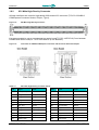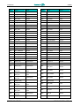
1
CPB906
Vortex86DX Based
COM Module
User Manual
Rev. 001 E
November 2010
P
R
E
L
I
M
I
N
A
R
Y
Product Title:
Document name:
Manual version:
Ref. doc. ver.:
CPB906
CPB906 User Manual
001 E
1.0 R (ИМЕС.421459.906 РЭ)
Copyright © 2010 Fastwel Co. Ltd. All rights reserved.
Revision Record
Rev. Index
Brief Description of Changes
Board Index
Date of Issue
001
Initial version
CPB906
November 2010
Contact Information
Fastwel Co. Ltd
Fastwel Corporation US
Address:
108 Profsoyuznaya st.,
Moscow 117437,
Russian Federation
45 Main Street, Suite 319
Brooklyn, New York 11201
USA
Tel.:
+7 (495) 232-1681
+1 (718) 554-3686
Fax:
+7 (495) 232-1654
+1 (718) 797-0600
Toll free:
E-mail:
[email protected]
Web:
http://www.fastwel.com/
+1 (877) 787-8443 (1-877-RURUGGED)
CPB906
Table of Contents
Table of Contents ..............................................................................................................................................1
List of Tables .....................................................................................................................................................2
List of Figures ....................................................................................................................................................3
Notation Conventions.........................................................................................................................................4
General Safety Precautions................................................................................................................................5
Unpacking, Inspection and Handling...................................................................................................................6
Three Year Warranty..........................................................................................................................................7
1
Introduction...................................................................................................................................... 8
1.1
1.2
1.3
1.4
1.5
1.6
1.7
1.8
2
Module Introduction.................................................................................................................................8
Main Specifications .................................................................................................................................8
Functional Diagram ...............................................................................................................................11
Appearance and Layout ........................................................................................................................12
CPB906 Versions..................................................................................................................................13
Delivery Checklist..................................................................................................................................13
Additional Accessories ..........................................................................................................................14
Functional Description...........................................................................................................................14
1.8.1
Vortex86DX SoC ..................................................................................................................14
1.8.2
XS1 Main High-Dencity Connector.........................................................................................15
1.8.3
Supervisor and Watchdog Timers..........................................................................................19
1.8.3.1
WDT0 and WDT1 Registers Description ................................................................19
1.8.4
SDRAM Memory...................................................................................................................23
1.8.5
Flash BIOS...........................................................................................................................23
1.8.6
ATA Flash Disk .....................................................................................................................23
1.8.7
IDE/SDIO Port ......................................................................................................................24
1.8.8
COM1, COM2 Serial Ports ....................................................................................................24
1.8.9
PS/2 Keyboard and Mouse Interface......................................................................................25
1.8.10
RTC and Battery ...................................................................................................................25
1.8.11
USB Interface .......................................................................................................................26
1.8.12
Fast Ethernet Interface..........................................................................................................26
1.8.13
FRAM...................................................................................................................................26
1.8.14
Remote Reset/Interrupt, Remote Power Fail Signal Source Ports ...........................................26
1.8.15
8-bit ISA Port ........................................................................................................................26
1.8.16
LPC Port...............................................................................................................................26
1.8.17
PCI Port (XS1)......................................................................................................................27
1.8.18
I2C Port................................................................................................................................27
1.8.19
GPIO Port.............................................................................................................................27
1.8.20
PC-Buzzer Port.....................................................................................................................27
1.8.21
LED indicators ......................................................................................................................27
1.8.22
Redundancy Port ..................................................................................................................28
Technical Information .....................................................................................................................29
2.1
2.2
2.3
2.4
2.5
2.6
C P B 9 0 6
Hardware Interrupts...............................................................................................................................29
DMA Channels......................................................................................................................................29
I/O Addressing ......................................................................................................................................30
Memory Addressing ..............................................................................................................................31
GPIO Processor Ports...........................................................................................................................31
Overall and Mounting Dimensions .........................................................................................................32
U s e r
M a n u a l
1
© 2 0 1 0
F a s t w e l
v . 0 0 1
E
CPB906
3
System Setup ..................................................................................................................................33
3.1
3.2
3.3
3.4
Safety Regulations ................................................................................................................................33
Jumper Settings ....................................................................................................................................34
Software Installation..............................................................................................................................34
AMI BIOS .............................................................................................................................................34
3.4.1
BIOS Setup Program. Introduction.........................................................................................34
Basic Software......................................................................................................................................35
Service Software...................................................................................................................................35
3.6.1
SPIFLASH.EXE Utility...........................................................................................................35
CPB906 Programming FAQ...................................................................................................................35
3.5
3.6
3.7
4
Appendices .....................................................................................................................................36
4.1
KIB880 Carrier Board ............................................................................................................................36
4.1.1
Introduction...........................................................................................................................36
4.1.2
Appearance and Layout ........................................................................................................36
4.1.3
Functional Diagram...............................................................................................................39
4.1.4
Specifications .......................................................................................................................39
4.1.5
Delivery Checklist .................................................................................................................41
4.1.6
External Connections ............................................................................................................41
List of Tables
Table 1.1:
Table 1.2:
Table 1.3:
Table 1.4:
Table 1.5:
Table 1.6:
Table 1.7:
Table 1.8:
Table 1.9:
Table 1.10:
Table 1.11:
Table 1.12:
Table 1.13:
Table 1.14:
Table 1.15:
Table 1.16:
Table 1.17:
Table 1.18:
Table 1.19:
Table 1.20:
Table 1.21:
Table 1.22:
Table 2.1:
Table 2.2:
Table 2.3:
Table 2.4:
Table 2.5:
Table 2.6:
Table 3.1:
C P B 9 0 6
U s e r
CPB906 Versions .......................................................................................................................13
CPB906 Additional Accessories ..................................................................................................14
XS1: Main High-Density Connector Pinout ..................................................................................15
WDT0 Restart Register...............................................................................................................19
WDT0 Port Address Index Register.............................................................................................19
WDT0 Port Data Register ...........................................................................................................19
WDT0 Timer Control Register .....................................................................................................20
WDT0 Event Selection Register ..................................................................................................20
WDT0 Timer Value CNT0 Register .............................................................................................20
WDT0 Timer Value CNT1 Register .............................................................................................21
WDT0 Timer Value CNT2 Register .............................................................................................21
WDT0 Timer Mode Register .......................................................................................................21
WDT1 Restart Register...............................................................................................................21
WDT1 Timer Control Register .....................................................................................................22
WDT1 Event Selection Register ..................................................................................................22
WDT1 Timer Value CNT0 Register .............................................................................................22
WDT1 Timer Value CNT1 Register .............................................................................................22
WDT1 Timer Value CNT2 Register .............................................................................................23
WDT1 Timer Mode Register .......................................................................................................23
Frequency Divider Values for Serial Ports ...................................................................................25
LED Indicators............................................................................................................................27
XP1 Redundancy Connector Pinout ............................................................................................28
Interrupt Settings........................................................................................................................29
DMA Channels ...........................................................................................................................29
I/O Address Space .....................................................................................................................30
Memory Address Mapping ..........................................................................................................31
Processor GPIO Control Registers..............................................................................................31
Processor GPIO Lines Description..............................................................................................32
Jumper Positions........................................................................................................................34
M a n u a l
2
© 2 0 1 0
F a s t w e l
v . 0 0 1
E
CPB906
List of Figures
Figure 1.1:
Figure 1.2:
Figure 1.3:
Figure 1.4:
Figure 1.5:
Figure 1.6:
Figure 2.1:
Figure 4.1:
Figure 4.2:
Figure 4.3:
Figure 4.4:
Figure 4.5:
CPB906 Block Diagram ..............................................................................................................11
CPB906 Module Appearance......................................................................................................12
CPB906 Main Components Layout .............................................................................................12
XS1 Main High-Dencity Connector ..............................................................................................15
Connection of CPB906 COM-Express Connector and the Carrier Board Counterpart....................15
Redundancy Connection.............................................................................................................28
CPB906: Overall and Mounting Dimensions ................................................................................32
KIB880 Appearance ...................................................................................................................36
KIB880 Main Components Layout: Top Side ...............................................................................37
KIB880 Main Components Layout: Bottom Side ..........................................................................38
KIB880 Block Diagram................................................................................................................39
KIB880 External Connections Diagram........................................................................................41
All information in this document is provided for reference only, with no warranty of its suitability for any specific purpose. This information has been thoroughly checked and
is believed to be entirely reliable and consistent with the product that it describes. However, Fastwel accepts no responsibility for inaccuracies, omissions or their
consequences, as well as liability arising from the use or application of any product or example described in this document.
Fastwel Co. Ltd. reserves the right to change, modify, and improve this document or the products described in it, at Fastwel's discretion without further notice. Software
described in this document is provided on an “as is” basis without warranty. Fastwel assumes no liability for consequential or incidental damages originated by the use of
this software.
This document contains information, which is property of Fastwel Co. Ltd. It is not allowed to reproduce it or transmit by any means, to translate the document or to convert
it to any electronic form in full or in parts without antecedent written approval of Fastwel Co. Ltd. or one of its officially authorized agents.
Fastwel and Fastwel logo are trademarks owned by Fastwel Co. Ltd., Moscow, Russian Federation. Ethernet is a registered trademark of Xerox Corporation. IEEE is a
registered trademark of the Institute of Electrical and Electronics Engineers Inc. Intel is a trademark of Intel Corporation. Geode is trademark of AMD. Microsoft is a
trademark of the Microsoft corporation. In addition, this document may include names, company logos and trademarks, which are registered trademarks and, therefore,
are property of their respective owners.
Fastwel welcomes suggestions, remarks and proposals regarding the form and the content of this Manual.
C P B 9 0 6
U s e r
M a n u a l
3
© 2 0 1 0
F a s t w e l
v . 0 0 1
E
CPB906
Notation Conventions
Warning, ESD Sensitive Device!
This symbol draws your attention to the information related to electro static sensitivity of your
product and its components. To keep product safety and operability it is necessary to handle
it with care and follow the ESD safety directions.
Warning!
This sign marks warnings about hot surfaces. The surface of the heatsink and some
components can get very hot during operation. Take due care when handling, avoid
touching hot surfaces!
Caution: Electric Shock!
This symbol warns about danger of electrical shock (> 60 V) when touching products or
parts of them. Failure to observe the indicated precautions and directions may expose your
life to danger and may lead to damage to your product.
Warning!
Information marked by this symbol is essential for human and equipment safety.
Read this information attentively, be watchful.
Note...
This symbol and title marks important information to be read attentively for your own benefit.
C P B 9 0 6
U s e r
M a n u a l
4
© 2 0 1 0
F a s t w e l
v . 0 0 1
E
CPB906
General Safety Precautions
This product was developed for fault-free operation. Its design provides conformance to all related
safety requirements. However, the life of this product can be seriously shortened by improper
handling and incorrect operation. That is why it is necessary to follow general safety and
operational instructions below.
Warning!
All operations on this device must be carried out by sufficiently
skilled personnel only.
Warning!
When handling this product, special care must be taken not to hit
the heatsink (if installed) against another rigid object. Also, be
careful not to drop the product, since this may cause damage
to the heatsink, CPU or other sensitive components as well.
Please, keep in mind that any physical damage to this product
is not covered under warranty.
Note:
This product is guaranteed to operate within the published
temperature ranges and relevant conditions. However, prolonged
operation near the maximum temperature is not recommended by
Fastwel or by electronic chip manufacturers due to thermal stress
related failure mechanisms. These mechanisms are common to all
silicon devices, they can reduce the MTBF of the product by
increasing the failure probability. Prolonged operation at the lower
limits of the temperature ranges has no limitations.
Caution, Electric Shock!
Before installing this product into a system and before installing
other devices on it, always ensure that your mains power is
switched off.
Always disconnect external power supply cables during all handling
and maintenance operations with this module to avoid serious
danger of electrical shock.
C P B 9 0 6
U s e r
M a n u a l
5
© 2 0 1 0
F a s t w e l
v . 0 0 1
E
CPB906
Unpacking, Inspection and Handling
Please read the manual carefully before unpacking the module or mounting the device into your
system. Keep in mind the following:
ESD Sensitive Device!
Electronic modules and their components are sensitive to static
electricity. Even a non-perceptible by human being static discharge
can be sufficient to destroy or degrade a component's operation!
Therefore, all handling operations and inspections of this product
must be performed with due care, in order to keep product integrity
and operability:
n
Preferably, unpack or pack this product only at EOS/ESD safe workplaces. Otherwise, it is
important to be electrically discharged before touching the product. This can be done by
touching a metal part of your system case with your hand or tool. It is particularly important
to observe anti-static precautions when setting jumpers or replacing components.
If the product contains batteries for RTC or memory back-up, ensure that the module is not
placed on conductive surfaces, including anti-static mats or sponges. This can cause shortcircuit and result in damage to the battery and other components.
Store this product in its protective packaging while it is not used for operational purposes.
n
n
Unpacking
The product is carefully packed in an antistatic bag and in a carton box to protect it against
possible damage and harmful influence during shipping. Unpack the product indoors only at a
temperature not less than +15°C and relative humidity not more than 70%. Please note, that if the
product was exposed to the temperatures below 0°С for a long time, it is necessary to keep it at
normal conditions for at least 24 hours before unpacking. Do not keep the product close to a heat
source.
Following ESD precautions, carefully take the product out of the shipping carton box. Proper
handling of the product is critical to ensure correct operation and long-term reliability. When
unpacking the product, and whenever handling it thereafter, be sure to hold the module preferably
by the front panel, card edges or ejector handles. Avoid touching the components and connectors.
Retain all original packaging at least until the warranty period is over. You may need it for
shipments or for storage of the product.
Initial Inspection
Although the product is carefully packaged, it is still possible that shipping damages may occur.
Careful inspection of the shipping carton can reveal evidence of damage or rough handling. Should
you notice that the package is damaged, please notify the shipping service and the manufacturer
as soon as possible. Retain the damaged packing material for inspection.
After unpacking the product, you should inspect it for visible damage that could have occurred
during shipping or unpacking. If damage is observed (usually in the form of bent component leads
or loose socketed components), contact Fastwel's official distributor from which you have
purchased the product for additional instructions. Depending on the severity of the damage, the
product may even need to be returned to the factory for repair. DO NOT apply power to the product
if it has visible damage. Doing so may cause further, possibly irreparable damage, as well as result
in a fire or electric shock hazard.
If the product contains socketed components, they should be inspected to make sure they are
seated fully in their sockets.
C P B 9 0 6
U s e r
M a n u a l
6
© 2 0 1 0
F a s t w e l
v . 0 0 1
E
CPB906
Handling
In performing all necessary installation and application operations, please follow only the
instructions supplied by the present manual.
In order to keep Fastwel’s warranty, you must not change or modify this product in any way, other
than specifically approved by Fastwel or described in this manual.
Technical characteristics of the systems in which this product is installed, such as operating
temperature ranges and power supply parameters, should conform to the requirements stated by
this document.
Retain all the original packaging, you will need it to pack the product for shipping in warranty cases
or for safe storage. Please, pack the product for transportation in the way it was packed by the
supplier.
When handling the product, please, remember that the module, its components and connectors
require delicate care. Always keep in mind the ESD sensitivity of the product.
Three Year Warranty
Fastwel Co. Ltd. (Fastwel), warrants that its standard hardware products will be free from defects
in materials and workmanship under normal use and service for the currently established warranty
period. Fastwel’s only responsibility under this warranty is, at its option, to replace or repair any
defective component part of such products free of charge.
Fastwel neither assumes nor authorizes any other liability in connection with the sale, installation
or use of its products. Fastwel shall have no liability for direct or consequential damages of any
kind arising out of sale, delay in delivery, installation, or use of its products.
If a product should fail through Fastwel's fault during the warranty period, it will be repaired free of
charge. For out of warranty repairs, the customer will be invoiced for repair charges at current
standard labor and materials rates.
Warranty period for Fastwel products is 36 months since the date of purchase.
The warranty set forth above does not extend to and shall not apply to:
1.
Products, including software, which have been repaired or altered by other than
Fastwel personnel, unless Buyer has properly altered or repaired the products in
accordance with procedures previously approved in writing by Fastwel.
2.
Products, which have been subject to power supply reversal, misuse, neglect,
accident, or improper installation.
Returning a product for repair
1.
Apply to Fastwel company or to any of the Fastwel's official representatives for the
Product Return Authorization.
2.
Attach a failure inspection report with a product to be returned in the form, accepted by
customer, with a description of the failure circumstances and symptoms.
3.
Carefully package the product in the antistatic bag, in which the product had been
supplied. Failure to package in antistatic material will VOID all warranties. Then
package the product in a safe container for shipping.
4.
The customer pays for shipping the product to Fastwel or to an official Fastwel
representative or dealer.
C P B 9 0 6
U s e r
M a n u a l
7
© 2 0 1 0
F a s t w e l
v . 0 0 1
E
Introduction
1
CPB906
Introduction
This document presents general information on CPB906 CPU module, the details of its proper and
safe installation, configuration and operation.
1.1
Module Introduction
CPB906 is the computer-on-module (COM) designed for use as a computing core in application
specific embedded systems. CPB906 module is based on 32-bit x86 compatible highly-integrated
Vortex86DX processor operating at 600 MHz with low power consumption and heat dissipation.
Small size (65x40 mm) of the CPB906 module together with low power consumption, high
performance and functional expandability provide decisions flexibility in modern real-time control
systems, industrial control systems, data aquisition and processing systems. It is equipped with
wide range of interfaces, such as ISA, PCI, IDE/2xSDIO, 2xUSB2.0, Ethernet 10/100 Mbit, I2C,
2xRS232 (TTL), and GPIO.
All basic interface signals are routed to carrier board through high-density 220-contact connector
(3-6318490-6, COM-Express Connector Socket 220-pin Type I, TYCO). Signals necessary for
building a redundancy system are routed to separate 10-contact connector (JST BM10B-SRSSTB, SMT Vertical Top Entry 10-pin Plug 1.00 mm, SH-Series).
1.2
Main Specifications
n
CPU: Integrated in DM&P Vortex86DX SoC
§
32-bit x86 x86 compatible core
§
16-bit memory bus
§
Math coprocessor
§
32 KB L1, 256 KB L2 cache
§
6-stage pipeline
n
System Memory
§
256 MB DDR2 SDRAM
§
Soldered onboard
§
DDR333
n
Flash-disk
§
1 GB NAND Flash (SLC)
§
Soldered onboard
§
Connected to Secondary Master IDE channel
§
Can be used as bootable device
C P B 9 0 6
U s e r
M a n u a l
8
© 2 0 1 0
F a s t w e l
v . 0 0 1
E
Introduction
CPB906
n
IDE port
§
One Primary channel
§
Connection of up to two external devices
§
UltraDMA 100 support
n
Flash BIOS
§
256 KB reserved. One copy in SPI-Flash embedded in processor,
another – external Flash on the carrier board – ISA bus
§
In-system modification
n
Ethernet port:
§
10/100 Mb/s
§
Operation mode LED indication
n
USB ports (host):
§
USB 1.1, USB 2.0 support
§
Connection of up to two devices
n
Serial ports:
§
COM1: RS-232 (5-wires, TTL-levels)
§
COM2: RS-232 (5-wires, TTL-levels)
§
Each port additionally supports automatic data flow control signal
§
Exchange rate: up to 115200 b/s
n
8-bit ISA expansion bus, 8/16 MHz
n
32-bit PCI expansion bus, 33 MHz
n
LPC expansion bus
n
PS/2 keyboard and mouse port
n
I2C port
n
Redundancy support
n
Digital input/output port:
§
6 CMOS/TTL lines (5 V level compatible)
§
2 lines of embedded in the processor address decoder GPCS0#, GPCS1#;
I/O or Memory address space
§
Input voltage: log. ‘0’ max 0.8 V, log. ‘1’ min 2.5 V
§
Output voltage: log. ‘0’ max 0.4 V @ 5 mA, log. ‘1’ min 2.4 V @ 2 mA
§
FPGA: XILINX XCS20-3TQ144I
n
Two hardware watchdog timers:
§
Embedded in the processor
§
Programmable: 30.5 ms … 512 s
n
64 Kbit FRAM for user data storage
n
Real time clock: power off consumption current 2 mA (normal conditions)
n
Onboard lithium battery: 3 V (CR2032; 180…200 mAh capacity)
n
Hardware reset/interrupt port
n
External Power Fail signal source port
n
Interrupt/reset generation on the power supply voltage drop below 4.7 V
n
PC-buzzer port
C P B 9 0 6
U s e r
M a n u a l
9
© 2 0 1 0
F a s t w e l
v . 0 0 1
E
Introduction
CPB906
n
Operatiing systems support:
§
Microsoft™ MS-DOS® 6.22
§
Fastwel™ FDOS 6.22
§
Microsoft™ Windows CE 5
§
Linux 2.6
§
QNX 6.4х
n
Console ports
§
COM1/COM2 and/or VGA/LCD (via an external video adapter)
and/or keyboard
n
Power supply voltage and consumption current:
§
Not more than 5 V (± 10%) @ 450 mA (without external devices)
§
Max. consumption current (including internal and external devices): 3 A
(limited by onboard fuse)
n
Additional power supply voltage generated by module for use by external devices on
the carrier board:
§
+3.3 V (± 5%) @ 400 mA
§
Max. current: 500 mA
§
Current is limited by self-resettable fuse
n
Operating temperature range:
§
Industrial: -40°..+85°C:(СPB906-01-I)
§
Commercial: 0°...+70°C (СPB906-01-C)
n
Relative humidity: up to 80%, non-condensing
n
Storage conditions: 1 under GOST 15150-69
n
Multiple shock resistance: 50 g
n
Vibration resistance: 5 g
n
MTBF: not less than 320000 hours
The value is calculated according to: Telcordia Issue 1 model, Method I Case 3, for continuous operation
at a surface location, at normal environmental conditions and at ambient temperature 30°С.
n
Dimensions: 65.2×40.2×10.5 mm
n
Weight: not more than 50 g
C P B 9 0 6
U s e r
M a n u a l
10
© 2 0 1 0
F a s t w e l
v . 0 0 1
E
Introduction
1.3
CPB906
Functional Diagram
Functional diagram of the CPB906 module is shown in the figure below.
Figure 1.1:
CPB906 Block Diagram
PS/2 Keyboard
& Mouse Port
IDE / 2xSDIO
Port
Ethernet
10/100 Mbit
NAND Flash
1 GB (SLC)
IDE Primary Channel
DDR2 SDRAM
256 MB
ATA Flash
Controller
North Bridge
16K Data
Cache
LPC Port
South Bridge
Vortex86DX SoC
MTBF
Counter
LPT
I2C Port
USB 2.0
2 x COM
+ / DDRII
SDRAM
I2C
Internal SPI Bus
GPIO
JTAG
Redundancy
External SPI Bus
RTC +
NVRAM 256 Bytes
Flash BIOS 2MB
COM1, COM2
RS232 (TTL)
LPC
10/100 Mbit LAN
16K Code
Cache
3.3 V @ 400 mA
Power Output
1.0V 1.8V 3.3V
IDE
Vortex86DX
CPU
DC/DC
IDE Secondary
Channel
2 x USB 2.0
XS1: SMT 220-pin
3-6318490-6 (TYCO)
5V Power
Input
6 GPIO + 2 Chip
Selector lines
(TTL)
32.768 KHz
3V Reset,
5V Power Fail Port
External Reset,
Power Fail Port
ISA
FRAM 64Kbit,
20 MHz
PCI
14.31818 MHz
External
WDT
PCI
8-bit ISA
XS2: JTAG
Connector
C P B 9 0 6
U s e r
M a n u a l
Battery
Battery
Port
XP1: Redundancy
Connector
11
© 2 0 1 0
F a s t w e l
v . 0 0 1
E
Introduction
1.4
CPB906
Appearance and Layout
Figure 1.2:
CPB906 Module Appearance
The appearance may vary for different versions of the module.
Figure 1.3:
CPB906 Main Components Layout
The layout may slightly differ for various versions of the module.
C P B 9 0 6
U s e r
M a n u a l
12
© 2 0 1 0
F a s t w e l
v . 0 0 1
E
Introduction
CPB906
Connectors of module are described in corresponding sections of this document. Switches X1…X5
are described in Jumper Settings section of this document.
1.5
CPB906 Versions
At the present time the CPB906 module is manufactured in four versions differing in operating
temperature range and protective coating.
Table 1.1:
CPB906 Versions
Version
Operating Temperature
Protective Coating
CPB906-01-I
-40°C to +85°C
–
CPB906-01-C
0°C to +70°C
–
CPB906-01-I \COATED
-40°C to +85°C
+
CPB906-01-C \COATED
0°C to +70°C
+
1.6
Delivery Checklist
The standard delivery checklist of CPB906 processor module includes:
1.
2.
3.
CPB906 processor module
CD-ROM with documentation and service software
Package
Note:
Keep the antistatic bag and the original package at least until
the warranty period is over. It can be used for future storage or
warranty shipments.
C P B 9 0 6
U s e r
M a n u a l
13
© 2 0 1 0
F a s t w e l
v . 0 0 1
E
Introduction
1.7
CPB906
Additional Accessories
Additional accessories are not supplied with the CPU module, are ordered separately.
Table 1.2:
CPB906 Additional Accessories
Name
Description
KIB880-01
Carrier board for CPB906 processor module
DVK906-01
Development kit including:
§ CPB906 processor module
§ KIB880 carrier board
§ VIM301 video processor module
§ Set of cables and adaptors
§
DVK906-02
CD with software and documentation including list of components
and electric schematic diagram of KIB880 carrier board
Development kit including in addition to DVK906-01 kit:
§ Windows CE 5.0 pre-installed on onboard flash-disk
DVK906-03
Development kit including in addition to DVK906-01 kit:
§ Linux 2.6 pre-installed on onboard flash-disk
1.8
Functional Description
1.8.1
Vortex86DX SoC
DM&P Vortex86DX includes the following main functional units:
n
n
n
n
n
n
n
n
n
n
n
n
n
n
n
n
n
C P B 9 0 6
32-bit х86 compatible core operating at 600 MHz;
32 KB L1, 256 KB L2 cache;
Math coprocessor;
16-bit DDR2 SDRAM memory bus;
IDE/SDIO controller;
RS-232 serial ports;
Universal parallel port;
Four USB 2.0 ports;
PS/2 keyboard/mouse port;
PCI, ISA, LPC, and SPI bus controllers;
I2C interface;
Built-in Ethernet 10/100 controller;
RTC;
CMOS memory for configuration storage;
Integrated flash-memory for BIOS storage;
Integrated redundancy system;
Two programmable watchdog timers.
U s e r
M a n u a l
14
© 2 0 1 0
F a s t w e l
v . 0 0 1
E
Introduction
1.8.2
CPB906
XS1 Main High-Dencity Connector
All basic interfaces are routed to high-density 220-contact XS1 connector (TYCO 3-6318490-6,
COM-Express Connector Socket, 220-pin, Type I).
Figure 1.4:
XS1 Main High-Dencity Connector
It is recommended to use as a counterpart on carrier board TYCO 3-1827253-6 (5 mm between
CPB906 and carrier board) or TYCO 3-6318491-6 (8 mm distance).
Figure 1.5:
Connection of CPB906 COM-Express Connector and the Carrier Board Counterpart
Table 1.3:
XS1: Main High-Density Connector Pinout
Pin#
Signal
In/Out
Pin#
Signal
In/Out
A1
GND (Fixed)
–
B1
GND (Fixed)
–
A2
ISA_GPCS1#
Output
B2
ISA_IOCHK#
Input
A3
ISA_GPCS0#
Output
B3
ISA_SD3
Input/Output
A4
ISA_SD6
Input/Output
B4
ISA_IOR#
Output
A5
ISA_SA5
Output
B5
ISA_IRQ9
Input
A6
ISA_SA1
Output
B6
ISA_DACK2#
Output
A7
ISA_SD2
Input/Output
B7
ISA_MEMW#
Output
A8
ISA_SD4
Input/Output
B8
ISA_MEMR#
Output
A9
ISA_SA2
Output
B9
ISA_SMEMR#
Output
A10
ISA_SA3
Output
B10
ISA_SMEMW#
Output
A11
GND (Fixed)
–
B11
GND (Fixed)
–
C P B 9 0 6
U s e r
M a n u a l
15
© 2 0 1 0
F a s t w e l
v . 0 0 1
E
Introduction
CPB906
Pin#
Signal
In/Out
Pin#
Signal
In/Out
A12
ISA_BCLK
Output
B12
ISA_OSC14M
Out, 14.318MHz
A13
ISA_SA4
Output
B13
ISA_AEN
Output
A14
ISA_SA19
Output
B14
ISA_IRQ5
Input
A15
ISA_SA17
Output
B15
ISA_IRQ7
Input
A16
ISA_SD0
Input/Output
B16
ISA_DACK3#
Output
A17
ISA_SA10
Output
B17
ISA_SA7
Output
A18
ISA_SD7
Input/Output
B18
ISA_DACK1#
Output
A19
ISA_SA8
Output
B19
ISA_IRQ6
Input
A20
ISA_SA9
Output
B20
ISA_IRQ4
Input
A21
GND (Fixed)
–
B21
GND (Fixed)
–
A22
ISA_SA18
Output
B22
ISA_IOCHRDY#
Input
A23
ISA_SD5
Input/Output
B23
ISA_IOW#
Output
A24
ISA_SA0
Output
B24
ISA_0WS#
Input
A25
ISA_SA6
Output
B25
ISA_REFRESH
Output
A26
ISA_SA14
Output
B26
ISA_TC
Output
A27
ISA_RST_DRV
Output
B27
ISA_IRQ3
Input
A28
ISA_SA15
Output
B28
ISA_DRQ2
Input
A29
ISA_DRQ3
Input
B29
ISA_BALE
Output
A30
ISA_ROMCS#
Output
B30
ISA_DRQ1
Input
A31
GND (Fixed)
–
B31
GND (Fixed)
–
A32
GPIO_P0_5
Input/Output
B32
ISA_SA13
Output
A33
GPIO_P0_3
Input/Output
B33
ISA_SD1
Input/Output
A34
GPIO_P0_0
Input/Output
B34
ISA_SA11
Output
A35
GPIO_P0_1
Input/Output
B35
ISA_SA12
Output
A36
GPIO_P0_4
Input/Output
B36
ISA_SA16
Output
A37
GPIO_P0_2
Input/Output
B37
IDE_D11
SD1_CLK
Input/Output
Output
A38
IDE_D7
SD0_WP
Input/Output
Input
B38
IDE_IOR#
Output
A39
IDE_D6
SD0_CD
Input/Output
Input
B39
IDE_DACK#
Output
A40
IDE_D8
SD1_D2
Input/Output
B40
IDE_IOW#
Output
A41
GND (Fixed)
–
B41
GND (Fixed)
–
A42
IDE_D14
SD1_CD
Input/Output
Input
B42
IDE_DRQ
Input
A43
IDE_CS1#
Output
B43
IDE_IORDY
Input
A44
IDE_D15
SD1_WP
Input/Output
Input
B44
IDE_INT
Input
A45
IDE_D4
SD0_D0
Input/Output
B45
IDE_A2
Output
A46
IDE_PDIAG#
Input
B46
IDE_D3
Input/Output
C P B 9 0 6
U s e r
M a n u a l
16
© 2 0 1 0
F a s t w e l
v . 0 0 1
E
Introduction
Pin#
CPB906
Signal
In/Out
Pin#
Signal
In/Out
SD0_CLK
Output
A47
IDE_D0
SD0_D2
Input/Output
B47
IDE_D1
SD0_D3
Input/Output
A48
IDE_A0
Output
B48
IDE_D9
SD1_D3
Input/Output
A49
IDE_CS0#
Output
B49
IDE_D5
SD0_D1
Input/Output
A50
SPK_DRV
Input/Output
B50
IDE_RST#
Output
A51
GND (Fixed)
–
B51
GND (Fixed)
–
A52
LAN_TX-
Output
B52
IDE_D2
SD0_CMD
Input/Output
A53
LAN_TX+
Output
B53
IDE_D10
SD1_CMD
Input/Output
A54
GND
B54
IDE_D12
SD1_D0
Input/Output
A55
LAN_RX+
Input
B55
IDE_A1
Output
A56
LAN_RX-
Input
B56
IDE_D13
SD1_D1
Input/Output
A57
GND
–
B57
GND
–
A58
USB0_D+
Input/Output
B58
USB1_D+
Input/Output
A59
USB0_D-
Input/Output
B59
USB1_D-
Input/Output
A60
GND (Fixed)
–
B60
GND (Fixed)
–
A61
COM1_RTS#
Output
B61
LAN_LED_ACTIVE#
Input/Output
A62
COM2_RTS#
Output
B62
LAN_LED_DUPLEX#
Input/Output
A63
COM2_TXD
Output
B63
CLOCK_24M
Output, 24 MHz
A64
COM1_TXD
Output
B64
LPC_AD3
Input/Output
A65
COM2_RXD
Input
B65
LPC_SERIRQ
Input/Output
A66
COM1_RXD
Input
B66
LPC_AD2
Input/Output
A67
COM2_TXEN
Output
B67
LPC_DRQ#
Input
A68
COM1_CTS#
Input
B68
LPC_AD0
Input/Output
A69
COM2_CTS#
Input
B69
LPC_AD1
Input/Output
A70
GND (Fixed)
–
B70
GND (Fixed)
–
A71
COM1_TXEN
Output
B71
LPC_FRAME#
Output
A72
RMT_PFO#
Input
B72
MS_DAT
Input/Output
A73
RMT_RESET#
Input
B73
KB_DAT
Input/Output
A74
PCI_AD2
Input/Output
B74
KB_CLK
Input/Output
A75
PCI_AD3
Input/Output
B75
MS_CLK
Input/Output
A76
PCI_AD4
Input/Output
B76
I2C_SDA
Input/Output
A77
PCI_AD0
Input/Output
B77
I2C_SCL
Input/Output
A78
PCI_INTA#
Input
B78
PCI_AD1
Input/Output
A79
PCI_AD12
Input/Output
B79
PCI_FRAME#
Input/Output
A80
GND (Fixed)
–
B80
GND (Fixed)
–
C P B 9 0 6
U s e r
M a n u a l
17
© 2 0 1 0
F a s t w e l
v . 0 0 1
E
Introduction
CPB906
Pin#
Signal
In/Out
Pin#
Signal
In/Out
A81
PCI_AD8
Input/Output
B81
PCI_CBE0#
Input/Output
A82
PCI_AD7
Input/Output
B82
PCI_DEVSEL#
Input/Output
A83
PCI_CBE1#
Input/Output
B83
PCI_AD6
Input/Output
A84
PCI_AD5
Input/Output
B84
PCI_PAR
Input/Output
A85
PCI_AD9
Input/Output
B85
PCI_AD11
Input/Output
A86
PCI_AD10
Input/Output
B86
PCI_AD15
Input/Output
A87
PCI_AD14
Input/Output
B87
PCI_AD16
Input/Output
A88
PCI_AD13
Input/Output
B88
PCI_CBE2#
Input/Output
A89
PCI_STOP#
Input/Output
B89
PCI_AD17
Input/Output
A90
GND (Fixed)
–
B90
GND (Fixed)
–
A91
PCI_RESET#
Output
B91
PCI_AD19
Input/Output
A92
PCI_IRDY#
Input/Output
B92
PCI_CLKB
Output
A93
PCI_TRDY#
Input/Output
B93
PCI_CLKA
Output
A94
PCI_CBE3#
Input/Output
B94
PCI_AD20
Input/Output
A95
PCI_AD26
Input/Output
B95
PCI_AD18
Input/Output
A96
PCI_AD25
Input/Output
B96
PCI_AD21
Input/Output
A97
PCI_GNT0#
Output
B97
PCI_AD31
Input/Output
A98
PCI_AD24
Input/Output
B98
PCI_INTC#
Input
A99
PCI_PREQ0#
Input/Output
B99
PCI_INTB#
Input
A100
GND (Fixed)
–
B100
GND (Fixed)
–
A101
PCI_AD30
Input/Output
B101
PCI_AD22
Input/Output
A102
PCI_PREQ1#
Input/Output
B102
PCI_AD23
Input/Output
A103
PCI_PREQ2#
Input/Output
B103
PCI_INTD#
Input
A104
PCI_AD28
Input/Output
B104
PCI_GNT2#
Output
A105
PCI_AD29
Input/Output
B105
PCI_GNT1#
Output
A106
PCI_AD27
Input/Output
B106
+3V
Output
A107
VBAT
Input/Output
B107
+3V
Output
A108
+5V_POWER
Input
B108
+5V_POWER
Input
A109
+5V_POWER
Input
B109
+5V_POWER
Input
A110
GND (Fixed)
–
B110
GND (Fixed)
–
C P B 9 0 6
U s e r
M a n u a l
18
© 2 0 1 0
F a s t w e l
v . 0 0 1
E
Introduction
1.8.3
CPB906
Supervisor and Watchdog Timers
CPB906 module includes power supply supervisor for monitoring of main voltages. Supervisor
forms hardware reset signal (hereinafter – RESET) if 3.3V power supply voltage drops below
3.08 V level, as well as NMI / IRQ / RESET signal if 5V input power supply voltage drops below
4.7 V level. This helps in saving user data in nonvolatile memory if it is necessary. RESET signal
generation on dropping the voltage below 4.7 V is enabled by a jumper switch (see the Jumper
Settings section).
Two watchdog timers WDT0 and WDT1 having programmable timeout period from 30.5 ms to 512
seconds are integrated in Vortex86DX SoC. WDT0 and WDT1 are controlled via internal processor
registers. Internal watchdog timers are enabled in BIOS Setup. The internal watchdog timers
timeout expiry does not lead to hardware RESET signal generation.
Watchdog timers are used to eliminate software hang-ups.
1.8.3.1
WDT0 and WDT1 Registers Description
Access to WDT0 timer registers is performed via port 65h and ports 22h (Index address register)
and 23h (Data register). To access the registers it is necessary to write the port address in 22h
port, data reading and/or writing is performed via port 23h. The detailed description of WDT0
watchdog timer control registers is given in Tables 1.4…1.12.
Access to WDT1 timer registers is performed via port 67h – 6Dh. The detailed description of WDT1
watchdog timer control registers is given in Tables 1.13…1.19.
Table 1.4:
Address
WDT0 Restart Register
Bits
Action
7
6
5
4
Write
65h
Read
3
2
1
0
-
-
-
-
3
2
1
0
-
-
-
RST_WDT0
-
-
-
-
Writing to this port leads to the WDT0 timer restart.
Table 1.5:
Address
WDT0 Port Address Index Register
Bits
Action
7
6
5
4
Write
22h
Read
ADDR_REG_WDT0
-
-
-
-
-
ADDR_REG_WDT0. Indicates address of chosen WDT0 watchdog timer register for access via
data register 23h.
Table 1.6:
Address
WDT0 Port Data Register
Bits
Action
7
23h
C P B 9 0 6
U s e r
6
5
4
3
Write
WRDATA_REG_WDT0
Read
WRDATA_REG_WDT0
M a n u a l
19
2
© 2 0 1 0
1
F a s t w e l
0
v . 0 0 1
E
Introduction
CPB906
WRDATA_REG_WDT0. Contains data for writing in the internal WDT0 timer register; the address
is indicated in the field ADDR_REG_WDT0 of address index register 22h.
WRDATA_REG_WDT0. Contains data while reading from the internal WDT0 timer register; the
address is indicated in the field ADDR_REG_WDT0 of address index register 22h.
Table 1.7:
WDT0 Timer Control Register
Bits (in Data Register 23h)
Address
(in Address
Register 22h)
Action
37h
(40h)
7
6
5
4
3
2
1
0
Write
-
WDT0_WE
-
-
-
-
-
-
Read
-
WDT0_WE
-
-
-
-
-
-
WDT0_WE. Enable/disable WDT0 watchdog timer operation:
1 – WDT0 enabled (default value);
0 – WDT0 disabled.
Table 1.8:
WDT0 Event Selection Register
Bits (in Data Register 23h)
Address
(in Address
Register 22h)
Action
7
Write
38h
(D0h)
6
5
4
3
2
1
0
1
0
WDT0_SSEL
Read
WDT0_SSEL. Event selection on WDT0 timeout expiry.
Bits
Event
Bits
Event
0000
Reserved
1000
IRQ[11]
0001
IRQ[3]
1001
IRQ[12]
0010
IRQ[4]
1010
IRQ[14]
0011
IRQ[5]
1011
IRQ[15]
0100
IRQ[6]
1100
NMI
0101
IRQ[7]
1101
Module reset (default value)
0110
IRQ[9]
1110
Reserved
0111
IRQ[10]
1111
Reserved
Table 1.9:
Address
(in Address
Register 22h)
39h
(00h)
WDT0 Timer Value CNT0 Register
Bits (in Data Register 23h)
Action
7
6
5
4
3
Write
WDT0_CNT0
Read
WDT0_CNT0
2
WDT0_CNT0. Bits [7:0] of WDT0_CNT [23:0] counter of WDT0 timer. LSB is 30.5 microseconds.
C P B 9 0 6
U s e r
M a n u a l
20
© 2 0 1 0
F a s t w e l
v . 0 0 1
E
Introduction
CPB906
Table 1.10:
WDT0 Timer Value CNT1 Register
Address
(in Address
Register 22h)
3Ah
(00h)
Bits (in Data Register 23h)
Action
7
6
5
4
3
Write
WDT0_CNT1
Read
WDT0_CNT1
2
1
0
WDT0_CNT1. Bits [15:8] of WDT0_CNT [23:0] counter of WDT0 timer. LSB is 30.5 microseconds.
Table 1.11:
WDT0 Timer Value CNT2 Register
Address
(in Address
Register 22h)
3Bh
(20h)
Bits (in Data Register 23h)
Action
7
6
5
4
3
Write
WDT0_CNT2
Read
WDT0_CNT2
2
1
0
WDT0_CNT2. Bits [23:16] of WDT0_CNT [23:0] counter of WDT0 timer. LSB is 30.5 microseconds.
Table 1.12:
WDT0 Timer Mode Register
Bits (in the data Register 23h)
Address
(in address
Register 22h)
Action
3Ch
(00h)
7
6
5
4
3
2
1
0
Write
WDT0_WDTF
WDT0_WDTRL
-
-
-
-
-
-
Read
WDT0_WDTF
-
-
-
-
-
-
-
WDT0_WDTF. WDT0 timer operation flag.
1 – There was timer operation (writing “1” in this bit resets the flag);
2 – There was no timer operation.
WDT0_WDTRL. WDT0 timer reset.
1 – WDT0-CNT counter reset;
0 – Writing of this value is not allowed.
Table 1.13:
Address
WDT1 Restart Register
Bits
Action
7
6
5
4
Write
67h
Read
3
2
1
0
-
-
-
RST_WDT1
-
-
-
-
-
Writing to this port leads to the WDT1 timer restart.
C P B 9 0 6
U s e r
M a n u a l
21
© 2 0 1 0
F a s t w e l
v . 0 0 1
E
Introduction
CPB906
Table 1.14:
WDT1 Timer Control Register
Address
Bits
Action
68h
(00h)
7
6
5
4
3
2
1
0
Write
-
WDT1_WE
-
-
-
-
-
-
Read
-
WDT1_WE
-
-
-
-
-
-
1
0
1
0
WDT1_WE. Enable/disable WDT1 watchdog timer operation.
1 – WDT1 enabled;
0 – WDT1 disabled (default value).
Table 1.15:
WDT1 Event Selection Register
Address
Bits
Action
7
Write
69h
(00h)
6
5
4
3
2
WDT1_SSEL
Read
WDT1_SSEL. Event selection on WDT1 timeout expiry.
Bits
Event
Bits
Event
0000
Reserved
1000
IRQ[11]
0001
IRQ[3]
1001
IRQ[12]
0010
IRQ[4]
1010
IRQ[14]
0011
IRQ[5]
1011
IRQ[15]
0100
IRQ[6]
1100
NMI
0101
IRQ[7]
1101
Module reset (default value)
0110
IRQ[9]
1110
Reserved
0111
IRQ[10]
1111
Reserved
Table 1.16:
Address
WDT1 Timer Value CNT0 Register
Bits
Action
7
6Ah
(00h)
6
5
4
3
Write
WDT1_CNT0
Read
WDT1_CNT0
2
WDT1_CNT0. Bits [7:0] of WDT1_CNT [23:0] counter of WDT1 timer. LSB is 30.5 microseconds.
Table 1.17:
Address
WDT1 Timer Value CNT1 Register
Bits (in the data Register 23h)
Action
7
6Bh
(00h)
C P B 9 0 6
U s e r
6
5
4
3
Write
WDT1_CNT1
Read
WDT1_CNT1
M a n u a l
22
2
© 2 0 1 0
1
0
F a s t w e l
v . 0 0 1
E
Introduction
CPB906
WDT1_CNT1. Bits [15:8] of WDT1_CNT [23:0] counter of WDT1 timer. LSB is 30.5 microseconds.
Table 1.18:
WDT1 Timer Value CNT2 Register
Address
Bits
Action
7
6Ch
(00h)
6
5
4
3
Write
WDT1_CNT2
Read
WDT1_CNT2
2
1
0
WDT1_CNT2. Bits [23:16] of WDT1_CNT [23:0] counter of WDT1 timer. LSB is 30.5 microseconds.
Table 1.19:
WDT1 Timer Mode Register
Address
Bits
Action
6Dh
(00h)
7
6
5
4
3
2
1
0
Write
WDT1_WDTF
-
-
-
-
-
-
-
Read
WDT1_WDTF
-
-
-
-
-
-
-
WDT1_WDTF. WDT1 timer operation flag.
1 – There was timer operation (writing “1” in this bit resets flag);
2 – There was no timer operation.
1.8.4
SDRAM Memory
DDR2 SDRAM memory chips operating at 333 MHz are soldered on board. Total memory size is
256 MB. Add-in memory modules installation is not supported.
1.8.5
Flash BIOS
Built in processor 2 MB SPI-Flash memory is used for BIOS storage.
Usage of external flash memory installed on a carrier board for storage of BIOS copy is enabled by
a set of signals: ISA_ROMCS#, ISA_MEMR#, and ISA_MEMW# routed to XS1 main high-density
connector.
In case flash memory chip for BIOS storage is installed on carrier board, it is necessary to provide
breaking of ISA_ROMCS# line between the main CPB906 connector and this flash memory chip in
order to enable booting using internal BIOS copy from built in processor SPI-Flash memory.
1.8.6
ATA Flash Disk
CPB906 has SST55LD019B ATA flash disk controller connected to Secondary master IDE
interface. The system detects this controller as an IDE disk which can be used as bootable; the
disk can be disabled in BIOS Setup. Standard IDE driver may be used for work with the disk. The
capacity of the soldered on-board NAND flash memory chip is 1 GB.
NAND flash disk contains the preinstalled FDOS 6.22 operating system compatible with MS DOS
6.22 and some software utilities providing operational availability of the module.
C P B 9 0 6
U s e r
M a n u a l
23
© 2 0 1 0
F a s t w e l
v . 0 0 1
E
Introduction
1.8.7
CPB906
IDE/SDIO Port
Two devices with IDE interface can be connected to the module (HDD, CompactFlash, CD/DVDROM etc.). To enable this, Primary IDE channel signals (“IDE_” prefix) are routed to the main XS1
connector; Master / Slave modes are supported. Modes up to UDMA-100 are supported by IDE
interface.
Alternatively, the port van be used for connection of two drives in SD-card format (“SD0_” and
“SD1_” prefixes). Connected devices will be detected as Primary Master and Primary Slave.
Primaty IDE port function (IDE or SD) is set in BIOS Setup.
Important:
Simultaneous connection of external IDE devices and SD cards is not
allowed. Before connecting external IDE devices to CPB906 make
sure that no SD slot is populated and “IDE” mode is selected for
Primary IDE in BIOS Setup. And vice versa, all IDE devices must be
physically disconnected and the channel must be set to “SD” mode in
BIOS Setup before connection of SD cards.
1.8.8
COM1, COM2 Serial Ports
The processor module has two asynchronous serial ports COM1 and COM2 routed to the main
XS1 connector (“COM1_” and “COM2_” prefixes). COM1 and COM2 ports operate as 5-wire
RS-232 interfaces (TTL-levels) and have standard PC/AT base addresses. Each port also includes
additional transfer direction automatic control signal for convenience in building of RS422/485 ports
on the basis of COM1 and COM2.
Both ports can be used for console input/output and files tranfer. By default, port COM1 is used for
console operation.
Maximum data transfer rate for COM1 and COM2 is 750 Kb/s. The ports are fully software
compatible with UART 16550.
Serial ports exchange rate is set in BIOS Setup. Exchange rate is determined by the value in
processor frequency divider register. Value of divider is calculated using the following equation:
DIV = F / (16 • BR), BR=F / (DIV • 16)
F – Internal oscillator frequency, 1.8432 or 24 MHz;
DIV – Divider value.
For F = 1.8432 MHz minimum value is DIV = 1;
for F = 24 MHz minimum value is DIV = 2;
BR – Required exchange rate, bit/sec.
Attention:
Receiver allows deviation of exchange rate value: -3.0 % and +2.5 %.
Frequency divider values for some exchange rates are given in the table below:
C P B 9 0 6
U s e r
M a n u a l
24
© 2 0 1 0
F a s t w e l
v . 0 0 1
E
Introduction
CPB906
Table 1.20:
Frequency Divider Values for Serial Ports
F = 1.8432 MHz
Exchange Rate,
bit/sec
F = 24 MHz
Divider
Error, %
Divider
Error, %
50
2304
-
30000
-
75
1536
-
20000
-
110
1047
-0.026
13636
-
150
768
-
10000
-
300
384
-
5000
-
600
192
-
2500
-
1200
96
-
1250
-
1800
64
-
833
-
2000
58
+0.69
750
-
2400
48
-
625
-
3600
32
-
417
-
4800
24
-
312
-
7200
16
-
208
-
9600
12
-
156
-
19200
6
-
78
-
38400
3
-
39
-
57600
2
-
26
-
115200
1
-
13
-
250000
-
-
6
-
256000
-
-
6
+2.34
375000
-
-
4
-
1.8.9
PS/2 Keyboard and Mouse Interface
PS/2 keyboard and mouse interface is routed to the main XS1 connector (signals with “KB_” and
“MS_” prefixes).
1.8.10
RTC and Battery
CPB906 module includes AT-compatible real time clock with lithium battery backup. Expected
battery life is about 10 years. However, the battery life depends greatly on operating and storage
temperatures, as well as on power off time. Therefore, it is recommended to replace the battery
approximately every four years.
Important!
Replacing the battery, observe polarity: “+” is up.
Dispose of used batteries according to the local regulations.
C P B 9 0 6
U s e r
M a n u a l
25
© 2 0 1 0
F a s t w e l
v . 0 0 1
E
Introduction
CPB906
It is possible to connect an external battery or to use the battery mounted on CPB906 module by
the carrier board (“RMT_VBAT” signal) if necessary. Battery power lines are routed to the main
XS1 high density connector.
1.8.11
USB Interface
The module has two USB 2.0 host ports routed to the main XS1 connector (signals with “USB0_”,
“USB1_” prefixes). Operation mode is selected in BIOS Setup. Each channel has separate power
control and protection circuit (+5V, 500 mA). One USB device may be connected to each port.
Booting from USB drive is supported.
1.8.12
Fast Ethernet Interface
One Fast Ethernet channel (10/100 Mb/s) is available via the main XS1 connector (signals with
“LAN_” prefix). Ethernet controller is integrated in Vortex86DX SoC. Two more signals can be used
for operation mode indication: LAN_LED_ACTIVE# - channel activity (active level ‘0’) and
LAN_LED_DUPLEX# - channel operation mode (active level ‘0’).
1.8.13
FRAM
FRAM is non-volatile memory with serial SPI interface. 8 KB are available to the user.
FRAM can be addressed directly via SPI registers, for details, please refer to Vortex86DX and
FRAM descriptions supplied on CD in ...\CPB906\Techinfo folder. A sample is available in
…\CPB906\Software\SFRAM906.zip file on the CD. (TBA)
1.8.14
Remote Reset/Interrupt, Remote Power Fail Signal Source Ports
To enable hardware reset signal from external RMT_RESET# signal (active level ‘0’) it is
necessary to close X5 jumper switch contacts.
To enable hardware reset signal from external RMT_PFO# signal (active level ‘0’) it is necessary to
close X2 jumper switch contacts.
1.8.15
8-bit ISA Port
8-bit ISA port includes all signals of standard 8-bit EISA expansion bus; it is routed to the main XS1
high density connector (signals with “ISA_” prefix).
1.8.16
LPC Port
LPC port includes all signals of standard LPC expansion bus and is routed to the main XS1 high
density connector (“LPC_” prefix).
C P B 9 0 6
U s e r
M a n u a l
26
© 2 0 1 0
F a s t w e l
v . 0 0 1
E
Introduction
1.8.17
CPB906
PCI Port (XS1)
PCI port includes standard 32-bit PCI bus signal set and is routed to the main XS1 high density
connector (“PCI_” prefix).
1.8.18
I2C Port
I2C port is routed to the main XS1 high density connector (“I2C_” prefix) and is intended for
connection of “slow” peripheral devices, such as temperature sensors, ADC, FRAM etc.
1.8.19
GPIO Port
GPIO port includes 6 CMOS/TTL lines (GPIO_P0(5:0) processor port) and 2 lines of built-in
processor address decoder – ISA_GPCS0# and ISA_GPCS1# signals. All port signals are routed
to the main XS1 high density connector.
1.8.20
PC-Buzzer Port
PC-buzzer port (“SPK_DRV” signal) is routed to the main XS1 connector.
1.8.21
LED indicators
Table 1.21:
LED Indicators
LED
Function
HL1
Built-in FFD activity (green)
HL2
Two-color user LED (red/green)
HL3
Diagnostic LED (green)
HL2 LED is controlled via GPIO_P2[0] (red) and GPIO_P2[1] (green) processor ports. HL3 LED
is controlled via GPIO_P0[7] processor port. Writing ‘0’ to GPIO port switches the corresponding
LED on, writing ‘1’ switches LED off.
C P B 9 0 6
U s e r
M a n u a l
27
© 2 0 1 0
F a s t w e l
v . 0 0 1
E
Introduction
1.8.22
CPB906
Redundancy Port
The redundancy port is routed to XP1 connector (JST BM10BSRSS-TB, SMT Vertical Top Entry
10-pin Plug 1.00 mm, SH-Series). It is used for connection to the other CPB906 module via the
hardware redundancy interface embedded in processor.
It is recommended to use SSH-003-P0.2-H contacts (10 items for one connector) and
JST SHR-10V-S housing as a counterpart.
Additional information on redundancy arrangement is available upon request.
Figure 1.6:
Redundancy Connection
Table 1.22:
XP1 Redundancy Connector Pinout
Pin #
Signal
In/Out
1
EXT_SYS_FAIL_OUT#
Output
2
EXT_SYS_FAIL_IN#
Input
3
RXD9
Input
4
TXD9
Output
5
GND
–
6
EXT_SYS_SWITCH_FAIL#
Input
7
EXT_GPCS#
Input
8
ISA_GPCS0#
Output
9
ISA_GPCS0#
Output
10
GND
–
C P B 9 0 6
U s e r
M a n u a l
28
© 2 0 1 0
F a s t w e l
v . 0 0 1
E
Technical Information
CPB906
2
Technical Information
2.1
Hardware Interrupts
Table 2.1:
Interrupt Settings
IRQ
Default Source
Alternative Sources
NMI
-
§
§
IRQ0
Reserved (system timer)
-
IRQ1
PS/2 Keyboard
-
IRQ2
Reserved (cascading)
-
IRQ3
COM2 (Vortex86DX)
External ISA devices (IRQ3)
IRQ4
COM1 (Vortex86DX)
External ISA devices (IRQ4)
IRQ5
External ISA devices (IRQ5)
-
IRQ6
External FDD / External ISA devices
Internal WDT
IRQ7
External ISA devices (IRQ7)
-
IRQ8
RTC
-
IRQ9
External ISA devices (IRQ9)
-
IRQ10
Ethernet controller & USB
-
IRQ11
Ethernet controller & USB
-
IRQ12
PS/2 Mouse
-
IRQ13
Reserved (coprocessor support)
-
IRQ14
Primary IDE (HDD, CompactFlash, …)
-
IRQ15
Secondary IDE (FFD)
-
2.2
DMA Channels
Table 2.2:
DMA Channels
DRQ
Source
DRQ0
–
DRQ1
External ISA devices
DRQ2
External ISA devices
DRQ3
External ISA devices
DRQ5
External ISA devices
DRQ6
External ISA devices
DRQ7
External ISA devices
C P B 9 0 6
U s e r
External ISA – devices (IOCHCK#)
Internal WDT
M a n u a l
29
© 2 0 1 0
F a s t w e l
v . 0 0 1
E
Technical Information
2.3
CPB906
I/O Addressing
Table 2.3:
I/O Address Space
Address
Function
0000h – 000Fh
Slave DMA
0020h – 0021h
Master Interrupt Controller
0022h – 0023h
Indirect Access
0040h – 0043h
Timer / Counter
0048h – 004Bh
PWM Control
0060h
0064h
Keyboard / Mouse Control
0061h
NMI Status / Control
0065h
0067h
WDT Reload
0068h – 006Dh
WDT Control
0070h – 0071h
CMOS Memory / RTC
0072h – 0075h
MTBF
0081h – 008BFh
DMA Page
0092h
System Control
00A0h – 00A1h
Slave Interrupt Controller
00C0h – 00DFh
Master DMA
0278h – 027Fh
LPT
0280h – 02BFh
ISA bus
02E8h – 02EFh
COM4
02F8h – 02FFh
COM2
03E8h – 03EFh
COM3
03F8h – 03FFh
COM1
0481h – 0483h
0487h
0489h – 048Bh
DMA High Page
0490h – 0499h
Interrupt Edge / Level Control
04D0h – 04D1h
Instruction Counter
0CF8h – 0CFFh
PCI Configuration
C P B 9 0 6
U s e r
M a n u a l
Note
30
© 2 0 1 0
F a s t w e l
v . 0 0 1
E
Technical Information
2.4
CPB906
Memory Addressing
Table 2.4:
Memory Address Mapping
Address Range
Function
Note
00000 – 9FFFFh
DOS
DOS area, 640 KB
A0000 – BFFFFh
VGA
Video memory area, 128 KB
C0000 – DFFFFh
NV RAM
ISA Expansion
Nonvolatile RAM / ISA devices
E0000 – EFFFFh
System BIOS
Extended System BIOS area, 64 KB (16KB×4)
F0000 – FFFFFh
System BIOS
System BIOS area, 64 KB
Address Range
Function
Note
10 0000 – Memory Top
DRAM
DDR2 SDRAM (256 MB installed)
Memory Top – FFE0 0000
PCI
PCI
FFE0 0000 – FFFF FFFFh
High BIOS
High BIOS area 2 MB (mapped to PCI)
2.5
GPIO Processor Ports
Vortex86DX includes four General Purpose Input Output ports (GPIO) available for user via
internal SoC registers. Every port consists of 8 input-output lines; each line may be set as input or
output by programming of the corresponding port registers.
Two 8-bit registers for each port are used to work with GPIO ports – Data register and Direction
register. Each data register bit conforms to the corresponding circuit on the board: Bit 0 conforms
to port line 0 (GPIO_Px0), Bit 7 conforms to port line 7 (GPIO_Px7) etc. Each direction register bit
conforms to the corresponding circuit on the board: Bit 0 conforms to port line 0 (GPIO_Px0), bit 7
conforms to port line 7 (GPIO_Px7) etc
Table 2.5:
Processor GPIO Control Registers
GPIO_P0
GPIO_P1
GPIO_P2
GPIO_P3
Data register
78h
79h
7Ah
7Bh
Direction register
98h
99h
9Ah
9Bh
C P B 9 0 6
U s e r
M a n u a l
31
Description
0: Line is input
1: Line is output
© 2 0 1 0
F a s t w e l
v . 0 0 1
E
Technical Information
Table 2.6:
CPB906
Processor GPIO Lines Description
Line
Direction
Description
GPIO_P0[5:0]
Input / Output
Lines are routed to 220-contact connector
GPIO_P0[6]
–
Not used
GPIO_P0[7]
Output
HL2 green LED control:
1 – LED is on,
0 – LED is off
GPIO_P1[0]
Input
Reserved
GPIO_P1[1]
Output
Reserved
GPIO_P1[2]
Input
Power Fail line state (supply voltage dropped below 4.75 V):
1 – Normal Operation,
0 – PF signal created
GPIO_P1[3]
Input
External Power Fail signal line state:
1 – Normal operation,
0 – External PF signal received
GPIO_P1[4]
Input
External Reset signal line state:
1 – Normal operation,
0 – External Reset signal received
GPIO_P1[5]
Input
Reserved
GPIO_P1[6]
Input
Reserved
GPIO_P1[7]
Input
Built-in NAND Flash controller state:
0 – On,
1 – Off.
Controlled only by BIOS program; control via the line is not allowed.
GPIO_P2[0]
Output
Two-colored HL3 – red LED control:
1 – LED is off,
0 – LED is on.
GPIO_P2[1]
Output
Two-colored HL3 – green LED control:
1 – LED is off,
0 – LED is on
GPIO_P2[7:2]
Input
Not used
GPIO_P3[3:0]
–
Reserved (SPI FRAM interface)
GPIO_P3[5:4]
–
Reserved (I2C interface)
GPIO_P3[6]
Input
Not used
GPIO_P3[7]
Input
Reserved
2.6
Overall and Mounting Dimensions
Figure 2.1:
CPB906: Overall and Mounting Dimensions
TBA
C P B 9 0 6
U s e r
M a n u a l
32
© 2 0 1 0
F a s t w e l
v . 0 0 1
E
System Setup
3
CPB906
System Setup
The following precautions must be observed to ensure proper installation and to avoid damage to
the module, other system components, or harm to personnel.
3.1
Safety Regulations
The following safety regulations must be observed when installing or operating the module.
Fastwel assumes no responsibility for any damage resulting from infringement of these rules.
The module can be installed on a carrier board with the compatible connector and properly
positioned mounting holes.
Warning!
Preferably, the module should not be placed on any surface or in
any kind of package until the module and its heatsink have cooled
down to ambient temperature.
ESD Sensitive Equipment!
This product comprises electrostatically sensitive components.
Please follow the ESD safety instructions to ensure module's
operability and reliability:
n
n
Use grounding equipment, if working at an anti-static
workbench. Otherwise, discharge yourself and the tools
in use before touching the sensitive equipment.
Try to avoid touching contacts, leads and components.
Extra caution should be taken in cold and dry weather.
Important!
When mounting the module on a carrier board make sure that the
Main connector of CPB906 is properly oriented in relation to its
counterpart connector. Misalignment of the connectors leads to
possible damage to the module and a carrier board.
To provide the declared mechanical and electric characteristics, the
use of supplied with the module fasteners and mounting hardware is
obligatory.
Mounting or dismounting the module on a carrier board with system
power on is not allowed. This can damage the module as well as a
carrier board.
C P B 9 0 6
U s e r
M a n u a l
33
© 2 0 1 0
F a s t w e l
v . 0 0 1
E
System Setup
3.2
CPB906
Jumper Settings
Some hardware configuration options are enabled with the help of X1 to X5 jumper switches.
X1 switch is used to switch between internal and external BIOS copies. X2 to X5 switches are used
to connect Power Fail, remote reset/interrupt signals to the hardware reset line of the processor.
“X# [0-0]” in the table below means that the jumper switch is open.
Table 3.1:
Jumper Positions
Jumper Position
Description
X1 [1-2]
Use of external BIOS copy enabled
X1 [0-0]
Internal BIOS copy (built in processor SPI Flash) enabled
X2 [1-2]
External Power Fail signal (from XS1 connector) is connected to the processor hardware
reset line
X3 [1-2]
Internal Power Fail signal (from internal power supply supervisor) is connected to the
processor hardware reset line
X5 [1-2]
External remote reset/interrupt signal (from XS1 connector) is connected to the processor
hardware reset line
3.3
Software Installation
The installation of the peripheral drivers is described in the accompanying information files. For
details on installation of an operating system, please refer to the relevant software documentation.
3.4
AMI BIOS
The AMI BIOS in CPB906 is an adapted version of a standard BIOS for IBM PC AT-compatible
personal computers equipped with x86 compatible processors. BIOS provides low-level support for
the central processing, memory, and I/O system units. System settings can be changed using the
BIOS Setup program.
3.4.1
BIOS Setup Program. Introduction
To enter the BIOS Setup program press “Del” on a keyboard connected to the module or F4 key on
a keyboard of a console PC provided the “Remote Control” option is enabled. With the BIOS Setup
program, you can modify BIOS settings and control special features of the module. The Setup
program offers a convenient menu interface to modify basic system configuration settings and
switching between the subsystems operation modes. These settings are stored in a dedicated
battery-backed memory, CMOS RAM, that keeps the information while the power is switched off.
The highlighted with grey fields are information fields intended to show system information and are
not available for editing.
Working with BIOS Setup, please refer to the integrated help system.
(TBA)
C P B 9 0 6
U s e r
M a n u a l
34
© 2 0 1 0
F a s t w e l
v . 0 0 1
E
System Setup
3.5
CPB906
Basic Software
CPB906 is delivered with the onboard NAND Flash disk containing programs providing operational
availability of the module:
§
§
§
FDOS (Fastwel DOS) operating system compatible with MS-DOS 6.22
Data tranfer service program (ftrans.exe)
Utility for system files transfer (sys.com)
3.6
Service Software
3.6.1
SPIFLASH.EXE Utility
The spiflash.exe service utility is intended for modification of the internal BIOS copy stored in
the SPI-Flash memory built in processor.
For modification of the SPI-Flas based BIOS it is necessary to run the utility with the "u" key and
the BIOS file name as a parameter:
spiflash u bios.rom
3.7
CPB906 Programming FAQ
Q: My C program “hangs” when a screen output function is called. What is the reason?
A: Part of screen output functions in high-level language library directly address registers and
memory of a graphics controller. If a CPB906 based system does not include a graphics controller,
calling such functions will result in complications. Selecting a screen output function, one should
consider its pecularities. Such information can always be found in the description of a library.
Q: Working with CPB906 module, I use SmartLink terminal program. I discovered that some files
tranferred to the module with the help of FTRANS.EXE program are saved in the module with
errors. What is the reason for that?
A: The reason is that SmartLink program for files transfer using FTRANS.EXE program employs
XMODEM protocol. This protocol has low transmission errors detection capability.
In order to completely avoid file transfer errors, it is strongly recommended not to use SmartLink
program. Instead, use a terminal program supporting XMODEM/CRC protocol
(e.g. HYPERTERMINAL, TELEMAX, TERM90, TERM95). To tranfer files, use FTRANS utility with
/CRC key.
C P B 9 0 6
U s e r
M a n u a l
35
© 2 0 1 0
F a s t w e l
v . 0 0 1
E
Appendices
CPB906
4
Appendices
4.1
KIB880 Carrier Board
This section contains brief description of KIB880 carrier board.
4.1.1
Introduction
KIB880 is an EPIC development board for CPB906 processor module, designed especially to
provide a quick start for CPB906-based applications. It can be used for initial software and
hardware development and debugging. KIB880 with CPB906 processor module can also be used
as a ready-to-use solution for some applications.
4.1.2
Appearance and Layout
Figure 4.1:
KIB880 Appearance
The appearance may vary for different versions of the module.
C P B 9 0 6
U s e r
M a n u a l
36
© 2 0 1 0
F a s t w e l
v . 0 0 1
E
Appendices
Figure 4.2:
CPB906
KIB880 Main Components Layout: Top Side
XP11
Power Connector
HL1
(+5V)
HL2
(+3.3V)
HL3
(+3.3V CPB)
HL5
HDD Activity
SW1
Reset Button
PC/104 (PCI)
XP49
XP34
1
XS6
XP31
PC/104+ (PCI)
XP12
Power Fail
XS3
MiniSD Socket
XP35
XP13
External
Reset
1
XP1
SMT 220-pin
Socket
1
XP32
1
XP33
XS7
XS4
MiniSD Socket
LPC47M107S
XP50
XP6
COM6
(RS232)
CY62128ELL
XS5 PC/104+ (ISA)
XP39
XS2
PS/2 Mouse
and Keyboard
1
1
RJ45
PS/2
XP5
COM5
(RS232)
XP38
1
1
DSub9
XS1
LAN
+ 2 USB
XP2
COM1(lower)
COM2 (upper)
(RS232)
XP3
XP10
COM1
GPIO
(RS485) (CPB906)
XP9
GPIO
(SIO)
XP4
COM2
(RS485)
XP7
LPT
XP14
IDE
The layout may slightly differ for various versions of the module.
C P B 9 0 6
U s e r
M a n u a l
37
© 2 0 1 0
F a s t w e l
v . 0 0 1
E
Appendices
Figure 4.3:
CPB906
KIB880 Main Components Layout: Bottom Side
XP8
CF Socket
The layout may slightly differ for various versions of the module.
C P B 9 0 6
U s e r
M a n u a l
38
© 2 0 1 0
F a s t w e l
v . 0 0 1
E
Appendices
4.1.3
CPB906
Functional Diagram
Functional diagram of the KIB880 carrier board is shown in the figure below.
Figure 4.4:
KIB880 Block Diagram
PS/2 Keyboard & Mouse
IDE
10/100 Mb LAN
CompactFlash
IDE
SD
LM92
Temp.
Sensor
Buzzer
SD
External PFO
FRAM
64 Kbit
FM24CL64
I2C
2 USB
External Reset
CPB906 Connector
6 GPIO Lines
Transceiver
COM1/COM2 (RS232)
PC/104+
RS232
Transceiver
LPC
8-bit ISA
PCI
COM1/COM2 (RS485)
RS485
8 GPIO Lines
SIO LPC47M107S
PC/104
NV SRAM 128 KB
ATX Connector 2x10 pin
RS232
Transceiver
CY62128EL
Vcc
+3.3V
4.1.4
LPT
COM5/COM6 (RS232)
BAT
MAX6368
BIOS AM29F040B
Specifications
n
Compatibility with CPB906
n
Form-factor: EPIC
n
Expansion modules support:
§
PC/104 (8-bit ISA);
§
PC/104+ (8-bit ISA, PCI)
n
IDE channel:
§
Shared with SDIO port;
§
Primary channel;
§
Up to two devices;
§
UltraDMA 100 support;
§
CompactFlash Type I/II socket
C P B 9 0 6
U s e r
M a n u a l
39
© 2 0 1 0
F a s t w e l
v . 0 0 1
E
Appendices
CPB906
n
SDIO channel:
§
shared with IDE port;
§
MiniSD cards support;
§
Up to two devices
n
LAN:
§
One 10/100 Mb/s Ethernet channel
§
MAC + PHY
§
Not less than 500 V isolation
n
USB:
§
USB 1.1, 2.0 (HS, FS, LS) support;
§
Up to two devices via Type A connectors
§
500 V isolation
n
Serial ports:
§
СОМ1, COM2: 4 wire RS232, up to 115200 b/s;
§
СОМ1, COM2: RS422/485, up to 115200 b/s;
§
Automatic data flow control signals supported;
§
СОМ5*, COM6*: via LPC47M107S SuperIO, RS232, up to 115200 b/s
n
Universal parallel port*:
§
SPP, EPP, ECP modes support
§
Via LPC47M107S SuperIO
n
PS/2 mouse and keyboard port
n
Discrete I/O ports (TTL, 5V):
§
6 channels via CPB906 GPIO;
§
8 channels via LPC SuperIO GPIO*.
n
External Reset & PFO (TTL, 5V)
n
Temperature sensor: NS LM92 (I2C port)
n
FRAM: 64 Kb (I2C port)
n
Flash memory (AM29F040) for reserve BIOS copy storage
n
Non-volatile SRAM:
§
128 KB
§
CPB906 battery support
n
Console operation via COM1, COM2 serial ports
§
(TBA)
n
Power supply:
§
+5 V ±5%
§
+12V and -12V routed from ATX connector to PC/104 lines
n
Power consumption:
§
0.1 A @ +5 V, 0.1 A @ +3.3 V
n
Operating temperature: –40°С to +85°С
n
MTBF: Not less than 400000 hours (TBA)
The value is calculated according to: Telcordia Issue 1 model, Method I Case 3, for continuous operation
at a surface location, at normal environmental conditions (Russian State Standard GOST 15150-69,
"UHL4" climatic parameters) and at ambient temperature 30°С.
C P B 9 0 6
U s e r
M a n u a l
40
© 2 0 1 0
F a s t w e l
v . 0 0 1
E
Appendices
CPB906
n
Stability:
§
Vibration: 5g
§
Single shock: 100g
§
Multiple shock: 50g
n
Weight: not more than 0.2 kg
Interfaces marked with (*) are not supported by BIOS version of 22.10.2009.
4.1.5
Delivery Checklist
1.
2.
3.
4.
5.
4.1.6
KIB880 module;
A set of counterparts for KIB880 connectors;
CD with software and documentation (developer's kit);
CD with software and documentation (standard Fastwel CD);
Consumer package
External Connections
Figure 4.5:
KIB880 External Connections Diagram
FAPI.685631.007
ATX
Power
Supply
External RESET
PC104+/PC104(8-bits) Modules
External PFO
ACS00031-03
XP11
PC/104 (PCI)
XP12 XP13
XS6
SW1
XP8
(bottom)
XS3
MiniSD
Socket
XP1
CF Socket
(bottom)
HCS0905H
CPB906
CPU
Module
XP32
MiniSD
Socket
XS4
XP33
XP6
XP14
XP50
XS5
XS1
XS2
PS/2
XP2
Modem
XP3
RJ45
+
2? USB
Two
DSub9
Category 5
Twisted Pair
XP4
XP5 FAPI.685611.020
XP10
XP9
XP7
HDD
SCD-128FF
ACS00031-01
General Purpose
I/O Signals
RS485
Network
Mouse and Keyboard
USB
Memory Modules
C P B 9 0 6
U s e r
M a n u a l
Ethernet
Switch
Printer
Console PC
41
© 2 0 1 0
F a s t w e l
v . 0 0 1
E