Download SiC401DB, SiC402DB, SiC403DB Reference Board User`s Manual

Transcript
SiC401DB, SiC402DB, SiC403DB
www.vishay.com
Vishay Siliconix
Reference Board User's Manual
THE CHIP
PRODUCT SUMMARY SiC401A/B
Input Voltage Range
3 V to 17 V
Output Voltage Range
0.6 V to 5.5 V
Operating Frequency
200 kHz to 1 MHz
Continuous Output Current
Peak Efficiency
Package
15 A
95 %
PowerPAK MLP55-32L
FEATURES
• SiC401 provides 15 A continuous output current capability
• SiC402 provides 10 A continuous output current capability
• SiC403 provides 6 A continuous output current capability
• Light Load Power Save Operation
- SiC401A, SiC402A and SiC403A:
minimum operating frequency fixed at 25 kHz
- SiC401B, SiC402B and SiC403B:
no minimum operating frequency
PRODUCT SUMMARY SiC402A/B
• Integrated bootstrap switch
Input Voltage Range
• Programmable 200 mA LDO with bypass logic
3 V to 28 V
Output Voltage Range
0.6 V to 5.5 V
Operating Frequency
200 kHz to 1 MHz
• Temperature compensated current limit
• Pseudo fixed-frequency adaptive on-time control
Continuous Output Current
10 A
• All ceramic solution enabled
Peak Efficiency
95 %
• Programmable input UVLO threshold
Package
PowerPAK MLP55-32L
PRODUCT SUMMARY SiC403A/B
Input Voltage Range
3 V to 28 V
Output Voltage Range
0.6 V to 5.5 V
Operating Frequency
200 kHz to 1 MHz
Continuous Output Current
Peak Efficiency
Package
6A
95 %
PowerPAK MLP55-32L
• Independent enable pin for switcher and LDO
• Programmable soft-start and soft-shutdown
• 1 % internal reference voltage
• Power good output
• Over-voltage and under-voltage protections
• PowerCAD simulation software available at
www.vishay.transim.com/login.aspx
• Material categorization: For definitions of compliance
please see www.vishay.com/doc?99912
DESCRIPTION
APPLICATIONS
The Vishay Siliconix SiC401A/B, SiC402A/B and SiC403A/B
are advanced stand-alone synchronous buck regulators,
featuring integrated power MOSFETs, bootstrap switch, and
a programmable LDO in a space-saving PowerPAK
MLP55-32L pin packages.
• Notebook, desktop and server computers
The SiC401A/B, SiC402A/B and SiC403A/B are capable of
operating with all ceramic solutions and switching
frequencies up to 1 MHz. The programmable frequency,
synchronous operation and selectable power-save feature
allow operation at high efficiency across the full range of
load current.
• Embedded applications
The internal LDO may be used to supply 5 V for the gate
drive circuits or it may be bypassed with an external
5 V for optimum efficiency and used to drive external
n-channel MOSFETs or other loads. Additional features
include cycle-by-cycle current limit, voltage soft-start,
under-voltage protection, programmable over-current
protection, soft shutdown and selectable power-save. Both
the SiC401A/B, SiC402A/B and SiC403A/B provides an
enable input and a power good output.
Revision: 22-Jan-14
• Digital HDTV and digital consumer applications
• Networking and telecommunication equipment
• Printers, DSL, and STB applications
• Point of load power supplies
ORDERING INFORMATION
DEMO BOARD PART NUMBER
MAX. OUTPUT CURRENT
SiC403DB
6A
SiC402DB
10 A
SiC401DB
15 A
Document Number: 62923
1
For technical questions, contact: [email protected]
THIS DOCUMENT IS SUBJECT TO CHANGE WITHOUT NOTICE. THE PRODUCTS DESCRIBED HEREIN AND THIS DOCUMENT
ARE SUBJECT TO SPECIFIC DISCLAIMERS, SET FORTH AT www.vishay.com/doc?91000
SiC401DB, SiC402DB, SiC403DB
www.vishay.com
Vishay Siliconix
THE REFERENCE BOARD
Input voltage (VDC): 3 V to 17 V for SiC401A/B or 3 V to 25 V
for SiC402A/B or 3 V to 25 V for SiC403A/B
Due to the nature of this controller, which requires a
minimum amount of ripple of 20 mVpp to operate properly,
if an all ceramic output solution is required, an additional
ripple injection circuit (R9, C19 and C24) must be used. This
will "artificially" generate ripple and apply it directly to the FB
pin while the output ripple is very low. More detail can be
found in the datasheet and in the output voltage ripple
section below.
Output voltage (VDC): 0.6 V to 5.5 V
CONNECTION AND SIGNAL/TEST POINTS
Output current (A): 15 A for SiC401A/B or 10 A for
SiC402A/B or 6 A for SiC403A/B
Power sockets
This reference board allows the end user to evaluate the
SiC401A/B, SiC402A/B and SiC403A/B for its features and
all functionalities. It can also be a reference design for a
user's application.
SPECIFICATION
Notes
• This board is, by default, preset to 1.2 V output with 12 V input
(Note: for inputs lower than 12 V, see “Input Voltage Range Adjustment”
(page 5))
• This board can be set to any output voltage between 0.6 V and
5.5 V, and any input voltage between 6 V and 28 V. For a specific
input/output voltage combination, the values of inductor and
ripple injection circuit may need to be modified..
• Since the internal LDO is set to 5 V, it is used to drive the VDD
input on the reference board. Input voltages lower then 5 V
require an external 5 V supply and should be connected to VDD
to bias the internal drivers and logic. Since an external source is
used, the internal LDO should be disabled by removing R6.
Efficiency is expected to be improved since the internal LDO is
not used.
INPUT CAPACITORS
The input capacitors are chosen as a combination of
electrolytic and ceramics so that the capacitance, the RMS
current, the ESR, the input voltage ripple and the cost can
be all fairly satisfied. For a combination of high voltage input
and low voltage output (low duty cycle), the electrolytic
capacitor (C12) may not be required. The reference board
uses 25 V input ceramics therefore, please limit Vin to 25 V
or less.
INDUCTORS
If off-the-shelf inductors are to be used, then their DCR
and saturation current parameters are key besides the
inductance values. The DCR causes an I2R loss, which
will decrease the system efficiency and generate heat. The
saturation current has to be higher than the maximum
output current plus 1/2 the ripple current. In over current
condition the inductor current may be very high. All this
needs to be considered when selecting the inductor. On this
board Vishay IHLP4040DZ or IHLP5050 series inductors are
used to meet cost requirement and get better efficiency.
OUTPUT CAPACITORS
Voltage, ESR and RMS current capability and capacitance
are essential elements to consider when choosing output
capacitors. The ESR and capacitance affect the output
voltage ripple, transient response and system stability. The
current capability determines the capacitor power
dissipation and life time. To meet all of these 4 requirements,
a combination of ceramics and tantalums can be used.
Revision: 22-Jan-14
VIN (B1), VIN_GND (B2): Input voltage source with VIN to be
positive. Connect to a 12 V to 25 V source that powers
SiC40xCD.
VO (B3), VO_GND (B4): Output voltage with VOUT to be
positive. Connect to a load that draws less than 15 A current.
Signal and test leads
VIN (P8), VIN_GND (P9): Input voltage sense pins with VIN to
be positive. An oscilloscope or Volt meter can be connected
to these terminals to measure or observe the input.
VO (P10), VOUT_GND (P11): Output voltage sense pins with
VO to be positive. An oscilloscope or Volt meter can be
connected to these terminals to measure or observe the
output.
VCTRL (P5), LDTRG (P4), VO_GND (P11): Load step control
signal input. Connect VCTRL and GND to a power source,
which supplies the correct voltage to generate the needed
load step. Connect LDTRG and GND to a pulse generater
that drives the MOSFET which is used for transient testing.
EN/PSV (P2): This pin on the SiC401A/B, SiC402A/B and
SiC403A/B have three functions: continuous run is enabled
by floating this pin, HI enables power save (PSV) and
grounding this pin disables switching. Continuous run mode
has poor light load efficiency which is typical in traditional
fixed frequency switchers. By enabling PSV light load,
efficiency is greatly improved. Connecting a jumper from
VDD (P1) to EN/PSV (P2) will pull this pin HI and PSV is
enabled. Tying this pin to ground disables switching.
ENL (P6): This pin is pulled up to VIN through a 100K resistor
and enables the internal adjustable LDO. An external power
source may be used by removing R6 and applying +5 V to
P1. The IC has an internal switchover circuit which improves
efficiency by tying VOUT to VLDO if VOUT is within ~ 0.5 V of
VLDO and disables the internal LDO. The default setting is
LDO enabled and VLDO is set to 5 V. Detailed description
can be found in the datasheet.
PGOOD (P7): This is an open drain output and is pulled up
with a 10K resistor. When the voltage at the FB pin is 10 %
below the nominal voltage, PGOOD is pulled low. It is held
low until the output voltage returns above -8 % of nominal.
PGOOD will transition low if the VFB pin exceeds +20 % of
nominal, which is also the over-voltage shutdown threshold.
PGOOD also pulls low if the EN/PSV pin is low when VDD is
present.
Document Number: 62923
2
For technical questions, contact: [email protected]
THIS DOCUMENT IS SUBJECT TO CHANGE WITHOUT NOTICE. THE PRODUCTS DESCRIBED HEREIN AND THIS DOCUMENT
ARE SUBJECT TO SPECIFIC DISCLAIMERS, SET FORTH AT www.vishay.com/doc?91000
SiC401DB, SiC402DB, SiC403DB
www.vishay.com
Vishay Siliconix
SET UP LOAD STEP
The hardware to test transient response is included in the
board, which allows users to see how the transient response
performs. The setup steps are:
1. Decide what load step is wanted, then based on the output
voltage calculate the external voltage VEXT that will be
connected between VCTRL and GND. For example, a load
step of 5 A between 0 A (I1) and 5 A (I2) is required and
the output voltage is 1.2 V. VEXT = VO - (I2 - I1) * 1  =
1.2 - (5 A - 0 A) * 1  = -3.8 V. Preset a DC source voltage
to VEXT = 3.8 V (current capability around 2 A) and connect
it to the board with positive side to GND and negative side
to VCTRL (if VEXT is a positive value, then connect the DC
source positive to VCTRL and negative to GND).
(Note: R4 need to change to 0.5  for the transient load step
test if the step output current is more than 7.5 A.)
2. Preset a waveform from a function generator using the
following parameters and set its output to OFF (refer to
the specific function generator manual for its setup):
Shape: Pulse
Frequency: 50 Hz or whatever is required
Duty cycle: ~ 0.1 % or whatever is required (keep
duration small so load step resistor will not be damaged)
Amplitude: +10 V level
Rising time and falling time: 1 μs or whatever is
required.
3. Connect the function generator output positive to
LDTRG and negative to GND.
4. Preset the current of an electronic load to I1 and turn it on.
5. Set up an oscilloscope using the following parameters.
Channel 1 for probing output voltage: AC coupled,
50 mV/div or whatever is required.
Channel 2 for probling the current on the 1  resistor
(R4) (use differential probe): DC coupled, 1 V/div
(corresponds to 1 A/div), for the step load current more
than 7.5 A, please use 0.5  resistor for R4. 1 V/div is
corresponds to 2 A/div. To view the output choke
current, a simpler method is to install a current loop
using 18AWG wire after the inductor and using a current
probe. Lift the side of the inductor connected to the
output caps and solder the loop of wire from the inductor
to where it was connected on the board. Keep the loop
of wire just big enough for the probe to fit. This will have
a slight delay in the waveform compared to the output
voltage, but is really used to varify the load step
amplitude is correct.
Time base: ~ 2 ms/div
Bandwidth: 20 MHz
6. Connect oscilloscope channel 1 probe positive to
VO (P10) and negative to VO_GND (P11), and channel 2
probe positive to VO (P10) and negative to
Step_I_SENSE (P3).
7. Turn on the system power. Output voltage should be
shown on the electronic load with current of I1.
8. Turn on the power source for VEXT.
9. Set the function generator output to be ON. The
transient response waveforms should be seen on the
oscilloscope.
10. If needed, re-adjust the trigger waveform’s rising and
falling time on the function generator so that the current
slew rate is satisfied (the current slew rate can be seen
on oscilloscope channel 2 waveform by setting the time
base to 1 μs or 500 ns).
11. To change load step, decrease or increase the value of
VEXT.
12. To cease transient response test, simply set the function
generator output to off, turn off the power source for
VEXT, and then shut down the system power.
Fig. 1 - SiC401A Transient Step Load Response in Forced Continuous Mode
Revision: 22-Jan-14
Document Number: 62923
3
For technical questions, contact: [email protected]
THIS DOCUMENT IS SUBJECT TO CHANGE WITHOUT NOTICE. THE PRODUCTS DESCRIBED HEREIN AND THIS DOCUMENT
ARE SUBJECT TO SPECIFIC DISCLAIMERS, SET FORTH AT www.vishay.com/doc?91000
SiC401DB, SiC402DB, SiC403DB
www.vishay.com
Vishay Siliconix
Fig. 2 - SiC401A Transient Step Load Response in Power Saving Mode
Efficiency (%)
90
85
80
75
70
65
60
55
50
45
40
35
30
25
20
Efficiency in FCM
0
2
4
6
Efficiency in PSV
8
10
Output Current (A)
12
14
16
14
16
Fig. 3 - SiC401A Efficiency
0.8
0.6
Load Regulaon (%)
Load Regulaon in FCM
Load Regulaon in PSV
0.4
0.2
0
-0.2
-0.4
-0.6
0
2
4
6
8
10
12
Output Current (A)
Fig. 4 - SiC401A Load Regulation
Revision: 22-Jan-14
Document Number: 62923
4
For technical questions, contact: [email protected]
THIS DOCUMENT IS SUBJECT TO CHANGE WITHOUT NOTICE. THE PRODUCTS DESCRIBED HEREIN AND THIS DOCUMENT
ARE SUBJECT TO SPECIFIC DISCLAIMERS, SET FORTH AT www.vishay.com/doc?91000
SiC401DB, SiC402DB, SiC403DB
www.vishay.com
OUTPUT VOLTAGE ADJUSTMENT
The evaluation board is configured for a 1.2 V output. If a
different output voltage is needed, simply change the value
of R23 based on the following formula:
Vishay Siliconix
Decreasing R9 will allow more signal through, hence more
ripple will be seen at the FB pin. Be sure to check that the
signal from the virtual ESR circuit is in phase with the output
ripple. C24 is a 0.1 μF capacitor.
VO = 0.6 * (1 + R10/R23) + Vripple/2
Where:
R10 is the upper resistor of the feedback voltage divider
R23 is the lower resistor of the feedback voltage divider
Vripple is the output ripple voltage.
See the following demo board schematic for R10 and R23.
INPUT VOLTAGE RANGE ADJUSTMENT
The input voltage range for this demo board is from 12 V to
25 V because a input power UVLO circuit is designed in to
protect the demo board. For the user who wants to explorer
the operation of the demo board in the lower input voltage,
he can remove the R52 to disable the input power UVLO
function of the demo board.
OUTPUT RIPPLE VOLTAGE
The controller used in the SiC40x requires at least of 20 mV
of ripple at the FB pin of the IC. This is easily attainable when
using a combination of output capacitors with higher ESR
like Electrolytic or Tantalum in parallel with low ESR
ceramic. The rule of thumb used for setting a limit for output
ripple voltage is a nominal 3 % of the output voltage. Using
this as a representative value and choosing a ripple current
(•I) that is between 20 % to 40 % of full load current we can
now calculate for an inductor value. By measuring the actual
ripple voltage using the values calculated so far and
adjusting one or more of the following: the inductor value,
number of output caps and Fsw used would lock in the final
values chosen for the design.
ESR = (0.03 * VOUT) / (0.4 * IOUTmax.)
using 40 % for the ripple current
Fig. 5 - Ripple Voltage Injection Circuit
Before adding a ripple injection circuit, the ripple voltage in
the feedback of the device need to be determined first to
make sure the ripple voltage is lower than 20 mV. The ripple
injection circuit is required only when the ripple voltage in
the feedback is lower than 20 mV. There may be difficulty
measuring the ripple voltage of feedback pin on the demo
board. However, it is recommended to measure the ripple
voltage on the output voltage VO. The ripple voltage on the
feedback can be easily calculated from the output ripple
voltage by the following formula.
VFB_ripple/Vripple = R23/ (R10 + R23)
Where: VFB_ripple is the ripple voltage on the feedback.
Vripple is the output ripple voltage.
R10 is the upper resistor of the feedback voltage divider.
R23 is the lower resistor of the feedback voltage divider.
L = [(VIN - VOUT) * (VOUT/(Fsw * VIN))] / [0.4 * (IOUTmax.)]
When an all ceramic output capacitor is used which limits
the amount of ripple voltage because of the very low ESR an
additional ripple voltage injection circuit consisting of 3
inexpensive passive components (R9, C19 and C24) is
needed. The network is a series RC connected across the
output inductor and a cap which couples this signal to the
FB pin. The objective is to stabilize the IC by increasing the
ripple at the FB pin by summing the ripple generated by this
ESR circuit with the low ripple generated by the ceramic
output capacitors. Using the following formula and the
circuit below we can get approximate values. For example,
L1 = 1 μH, DCR of inductor = 3.5 m, Let R1 = 3K solving
for C1 we get
L1/DCR = R9 * C19
C19 = (1 μH/3.5 m)/3K = 95 nF = 0.1 μF
Revision: 22-Jan-14
Document Number: 62923
5
For technical questions, contact: [email protected]
THIS DOCUMENT IS SUBJECT TO CHANGE WITHOUT NOTICE. THE PRODUCTS DESCRIBED HEREIN AND THIS DOCUMENT
ARE SUBJECT TO SPECIFIC DISCLAIMERS, SET FORTH AT www.vishay.com/doc?91000
SiC401DB, SiC402DB, SiC403DB
www.vishay.com
Vishay Siliconix
SCHEMATIC OF DEMO BOARD
Revision: 22-Jan-14
Document Number: 62923
6
For technical questions, contact: [email protected]
THIS DOCUMENT IS SUBJECT TO CHANGE WITHOUT NOTICE. THE PRODUCTS DESCRIBED HEREIN AND THIS DOCUMENT
ARE SUBJECT TO SPECIFIC DISCLAIMERS, SET FORTH AT www.vishay.com/doc?91000
SiC401DB, SiC402DB, SiC403DB
www.vishay.com
Vishay Siliconix
BILL of MATERIAL for SiC401A
ITEM QTY
1
4
2
3
REFERENCE
PCB
VALUE VOLTAGE
FOOTPRINT
DESCRIPTION
PART NUMBER
C1, C2, C3, C4
SM1210
22 μF
16 V
CAP, 22 μF, 16 V, 1210
GRM32ER71C226ME18L
1
C5
SM0402
0.1 μF
10 V
CAP, 0.1 μF, 10 V, 0402
VJ0402Y104MXQCW1BC
4
C6, C7, C11, C14
SM0603
0.1 μF
50 V
CAP, 0.1 μF, 50 V, 0603
VJ0603Y104KXACW1BC
4
3
C10, C20, C22
593D
68 μF
20 V
68 μF, TAN, 20 V, 593D, 20 %
593D686X0020D2TE3
5
1
C12
Radial
150 μF
35 V
Cap, Radial, 150 μF, 35 V
EU-FM1V151
6
1
C13
SM0402
0.01 μF
50 V
CAP, 0.01 μF, 50 V, 0402
VJ0402Y103KXACW1BC
7
4
C15, C21, C18A,
C18B for SiC401
SM1812
100 μF
10 V
CAP CER 100 μF, 10 V, 20 %,
X5R, 1206
C3216X5R1A107M160AC
8
1
C30
SM0402
68 pF
50 V
CAP, 68 pF, 50 V, 0402
VJ0402Y680KXACW1BC
9
1
C26
SM0805
4.7 μF
10 V
4.7 μF, 10 V, 0805
LMK212B7475KG-T
10
1
C28
SM0402
0.1 μF
10 V
CAP, 0.1 μF, 10 V, 0402
VJ0402Y104MXQCW1BC
11
1
C29
SM0603
22 nF
25 V
CAP,CER 22 nF, 25 V
VJ0603Y223KXACW1BC
12
1
C36
SM0402
560 pF
50 V
CAP, 560 pF, 0402
VJ0402A561KXAPW1BC
13
1
C37
SM0402
10 nF
50 V
CAP, 10 nF, 50 V, 0402
VJ0402A103KXACW1BC,
GRM155R71H103KA88D
14
1
L1 for SiC401
IHLP4040
0.56 μH
0.56 μH
IHLP4040DZERR56M01
15
11
P1, P2, P3, P4, P5,
P6, P7, P8, P9,
P10, P11
Terminal
0
0
Test points
1573-3
16
1
Q1
SO-8
0
30 V
N-Channel 30 V (D-S) MOSFET
with Schottky Diode
0
17
1
R1
SM0603
300K
50 V
RES, 300K , 1/10 W, 5 %
CRCW0603300KJNEA
18
1
R2
SM0603
100K
50 V
RES, 100K, 0603
CRCW0603100KFKEA
19
1
R4
SM2512
1
200 V
1 , 2512
CRCW25121R00FKEG
20
2
R5, R6
SM0603
100K
50 V
RES, 100K, 0603
CRCW0603100KFKEA
21
1
R7
SM0603
0
50 V
RES 0 
CRCW06030000ZOEA
22
1
R8
SM0603
12.4K
50 V
RES, 12.4K, 0603
CRCW060312K4FKEA
23
1
R10
SM0603
5.11K
50 V
RES, 5.11K, 0603
CRCW06035K11FKEA
24
1
R29
SM0603
10K
50 V
RES, 10K , 50 V ,0603
CRCW060310KFKED
25
1
R12
SM0603
57.6K
50 V
RES, 57.6K, 0603
CRCW060357K6FKEA
26
1
R13
SM0402
100 
50 V
100R, 50 V, 0402
CRCW0402100RFKED
27
1
R14
SM0402
100 
50 V
100R, 50 V, 0402
CRCW0402100RFKED
28
1
R15
SM0603
10K
50 V
RES, 10K, 50 V, 0603
CRCW060310KFKED
29
1
R23
SM0603
5.11K
50 V
RES, 5.11K, 0603
CRCW06035K11FKEA
30
1
R30
SM0603
69.8K
50 V
RES, 69.8K, 0603
CRCW060369K8FKEA
31
1
R39
SM0402
0
50 V
0R, 50 V, 0402
CRCW04020000ZOED
32
1
R51
SM0805
3.3R
50 V
RES, 3.3R, 0805
CRCW08053R3FKEA
33
1
R52
SM0603
31.6K
50 V
RES, 31.6K, 50 V, 0603
CRCW060331K6FKEA
34
1
U1
MLP55-32L
0
0
SiC401B MicroBuck Regulator
0
35
4
B1, B2, B3, B4
0
0
0
BANANA JACK
575-4
36
1
R9 for SiC401
SM0603
33.2K
RES, 33.2K  1/10W, 1 %, 0603 SMD
CRCW060333K2FKEA
37
1
C24
SM0603
820 pF
CAP, CER, 820 pF, 50 V, 5 %, NP0, 0603
C1608C0G1H821J080AA
38
1
C19
SM0603
10 nF
CAP, CER, 10 000 pF, 10 V, 10 %,
X5R, 0201
C0603X5R1A103K030BA
39
1
PCB
Revision: 22-Jan-14
SiC401/2/3 Demo Board PCB
Document Number: 62923
7
For technical questions, contact: [email protected]
THIS DOCUMENT IS SUBJECT TO CHANGE WITHOUT NOTICE. THE PRODUCTS DESCRIBED HEREIN AND THIS DOCUMENT
ARE SUBJECT TO SPECIFIC DISCLAIMERS, SET FORTH AT www.vishay.com/doc?91000
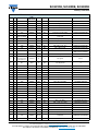
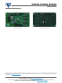
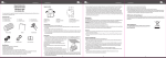
SiC401DB, SiC402DB, SiC403DB
www.vishay.com
Vishay Siliconix
BILL of MATERIAL for SiC402A
ITEM QTY
REFERENCE
PCB
VALUE VOLTAGE
FOOTPRINT
DESCRIPTION
PART NUMBER
1
4
C1, C2, C3, C4
SM1210
22 μF
16 V
CAP, 22 μF, 16 V, 1210
GRM32ER71C226ME18L
2
1
C5
SM0402
0.1 μF
10 V
CAP, 0.1 μF, 10 V, 0402
VJ0402Y104MXQCW1BC
3
4
C6, C7, C11, C14
SM0603
0.1 μF
50 V
CAP, 0.1 μF, 50 V, 0603
VJ0603Y104KXACW1BC
4
3
C10, C20, C22
593D
68 μF
20 V
68 μF, TAN, 20 V, 593D, 20 %
593D686X0020D2TE3
5
1
C12
Radial
150 μF
35 V
CAP, Radial, 150 μF, 35 V
EU-FM1V151
6
1
C13
SM0402
0.01 μF
50 V
CAP, 0.01 μF, 50 V, 0402
VJ0402Y103KXACW1BC
7
3
C15, C21,
C18 for SiC402
SM1206
100 μF
10 V
CAP, CER, 100 μF, 10 V, 20 %,
X5R, 1206
C3216X5R1A107M160AC
8
1
C30
SM0402
68 pF
50 V
CAP, 68 pF, 50 V, 0402
VJ0402Y680KXACW1BC
9
1
C26
SM0805
4.7 μF
10 V
4.7 μF, 10 V, 0805
LMK212B7475KG-T
10
1
C28
SM0402
0.1 μF
10 V
CAP, 0.1 μF, 10 V, 0402
VJ0402Y104MXQCW1BC
11
1
C29
SM0603
22 nF
25 V
CAP, CER, 22 nF, 25 V
VJ0603Y223KXACW1BC
12
1
C36
SM0402
560 pF
50 V
CAP, 560 pF, 0402
VJ0402A561KXAPW1BC
C37
SM0402
10 nF
50 V
CAP, 10 nF, 50 V, 0402
VJ0402A103KXACW1BC,
GRM155R71H103KA88D
1
L1
IHLP4040
1 μH
0
1 μH
IHLP4040DZER1R0M01
15
11
P1, P2, P3, P4,
P5, P6, P7, P8,
P9, P10, P11
Terminal
0
0
Test points
1573-3
16
1
Q1
SO-8
0
30 V
N-Channel 30 V (D-S) MOSFET with
Schottky Diode
0
17
1
R1
SM0603
300K
50 V
RES 300K , 1/10 W, 5 %
CRCW0603300KJNEA
18
1
R2
SM0603
100K
50 V
RES, 100K, 0603
CRCW0603100KFKEA
19
1
R4
SM2512
1
200 V
1 , 2512
CRCW25121R00FKEG
20
2
R5, R6
SM0603
100K
50 V
RES, 100K, 0603
CRCW0603100KFKEA
21
1
R7
SM0603
0
50 V
RES, 0 
CRCW06030000ZOEA
22
1
R8
SM0603
11K
50 V
RES, 11K, 0603
CRCW060311K0FKEA
23
1
R10
SM0402
5.11K
50 V
RES, 5.11K, 0402
CRCW04025K11FKED
24
1
R29
SM0603
10K
50 V
RES, 10K, 50 V, 0603
CRCW060310KFKED
25
1
R12
SM0603
57.6K
50 V
RES, 57.6K, 0603
CRCW060357K6FKEA
26
1
R13
SM0402
100 
50 V
100R, 50 V, 0402
CRCW0402100RFKED
27
1
R14
SM0402
100 
50 V
100R, 50 V, 0402
CRCW0402100RFKED
28
1
R15
SM0603
10K
50 V
RES, 10k, 50 V, 0603
CRCW060310KFKED
29
1
R23
SM0402
5.11K
50 V
RES, 5.11K, 0402
CRCW04025K11FKED
30
1
R30
SM0603
69.8K
50 V
RES, 69.8K, 0603
CRCW060369K8FKEA
31
1
R39
SM0402
0
50 V
0R, 50 V, 0402
CRCW04020000ZOED
32
1
R51
SM0805
3.3R
50 V
RES, 3.3R, 0805
CRCW08053R3FKEA
33
1
R52
SM0603
31.6K
50 V
RES, 31.6K, 50 V, 0603
CRCW060331K6FKEA
34
1
U1
MLP55-32L
0
0
SiC402B MicroBuck Regulator
0
35
4
B1, B2, B3, B4
0
0
0
BANANA JACK
575-4
36
1
R9 for SiC402
SM0603
26.7K
RES, 26.7K , 1/10 W, 1 %, 0603 SMD
CRCW060326K7FKEA
37
1
C24
SM0603
820 pF
CAP, CER, 820 pF, 50 V, 5 %, NP0 0603
C1608C0G1H821J080AA
38
1
C19
SM0603
10 nF
CAP, CER, 10 000 pF, 10 V, 10 %,
X5R, 0201
C0603X5R1A103K030BA
39
1
PCB
13
1
14
Revision: 22-Jan-14
SiC401/2/3 Demo Board PCB
Document Number: 62923
8
For technical questions, contact: [email protected]
THIS DOCUMENT IS SUBJECT TO CHANGE WITHOUT NOTICE. THE PRODUCTS DESCRIBED HEREIN AND THIS DOCUMENT
ARE SUBJECT TO SPECIFIC DISCLAIMERS, SET FORTH AT www.vishay.com/doc?91000
SiC401DB, SiC402DB, SiC403DB
www.vishay.com
Vishay Siliconix
BILL of MATERIAL for SiC403A
ITEM QTY
REFERENCE
PCB
VALUE VOLTAGE
FOOTPRINT
DESCRIPTION
PART NUMBER
1
4
C1, C2, C3, C4
SM1210
22 μF
16 V
CAP, 22 μF, 16 V, 1210
GRM32ER71C226ME18L
2
1
C5
SM0402
0.1 μF
10 V
CAP, 0.1 μF, 10 V, 0402
VJ0402Y104MXQCW1BC
3
4
C6, C7, C11, C14
SM0603
0.1 μF
50 V
CAP,0.1 μF, 50 V, 0603
VJ0603Y104KXACW1BC
4
2
C10, C20
593D
68 μF
20 V
68 μF, TAN, 20 V, 593D, 20 %
593D686X0020D2TE3
5
1
C12
Radial
150 μF
35 V
CAP, Radial, 150 μF, 35 V
EU-FM1V151
6
1
C13
SM0402
0.01 μF
50 V
CAP, 0.01 μF, 50 V, 0402
VJ0402Y103KXACW1BC
7
2
C15, C21 for
SiC403
SM1206
100 μF
10 V
CAP, CER, 100 μF, 10 V, 20 %,
X5R, 1206
C3216X5R1A107M160AC
8
1
C30
SM0402
68 pF
50 V
CAP, 68 pF, 50 V, 0402
VJ0402Y680KXACW1BC
9
1
C26
SM0805
4.7 μF
10 V
4.7 μF, 10 V, 0805
LMK212B7475KG-T
10
1
C28
SM0402
0.1 μF
10 V
CAP, 0.1 μF, 10 V, 0402
VJ0402Y104MXQCW1BC
11
1
C29
SM0603
22 nF
25 V
CAP, CER, 22 nF, 2 5 V
VJ0603Y223KXACW1BC
12
1
C36
SM0402
560 pF
50 V
CAP, 560pF, 0402
VJ0402A561KXAPW1BC
C37
SM0402
10 nF
50 V
CAP, 10 nF, 50 V, 0402
VJ0402A103KXACW1BC,
GRM155R71H103KA88D
1
L1 for SiC403
IHLP2525
1.5 μH
0
1.5 μH
IHLP2525CZER1R5M01
15
11
P1, P2, P3, P4,
P5, P6, P7, P8,
P9, P10, P11
Terminal
0
0
Test points
1573-3
16
1
Q1
SO-8
0
30 V
N-Channel 30 V (D-S) MOSFET with
Schottky Diode
0
17
1
R1
SM0603
300K
50 V
RES, 300K , 1/10 W, 5 %
CRCW0603300KJNEA
18
1
R2
SM0603
100K
50 V
RES, 100K, 0603
CRCW0603100KFKEA
19
1
R4
SM2512
1
200 V
1 , 2512
CRCW25121R00FKEG
20
2
R5, R6
SM0603
100K
50 V
RES, 100K, 0603
CRCW0603100KFKEA
21
1
R7
SM0603
0
50 V
RES, 0 
CRCW06030000ZOEA
22
1
R8
SM0603
10K
50 V
RES, 10K, 50 V, 0603
CRCW060310KFKED
23
1
R10
SM0402
5.11K
50 V
RES, 5.11K, 0402
CRCW04025K11FKED
24
1
R29
SM0603
10K
50 V
RES, 10K, 50 V, 0603
CRCW060310KFKED
25
1
R12
SM0603
57.6K
50 V
RES, 57.6K, 0603
CRCW060357K6FKEA
26
1
R13
SM0402
100 
50 V
100R, 50 V, 0402
CRCW0402100RFKED
27
1
R14
SM0402
100 
50 V
100R, 50 V, 0402
CRCW0402100RFKED
28
1
R15
SM0603
10K
50 V
RES, 10K, 50 V, 0603
CRCW060310KFKED
29
1
R23
SM0402
5.11K
50 V
RES, 5.11K, 0402
CRCW04025K11FKED
30
1
R30
SM0603
69.8K
50 V
RES, 69.8K, 0603
CRCW060369K8FKEA
31
1
R39
SM0402
0
50 V
0R, 50 V, 0402
CRCW04020000ZOED
32
1
R51
SM0805
3.3R
50 V
RES, 3.3R, 0805
CRCW08053R3FKEA
33
1
R52
SM0603
31.6K
50 V
RES, 31.6K, 50 V, 0603
CRCW060331K6FKEA
34
1
U1
MLP55-32L
0
0
SiC403B MicroBuck Regulator
0
35
4
B1, B2, B3, B4
0
0
0
BANANA JACK
575-4
36
1
R9 for SiC403
SM0603
10.7K
RES, 10.7K , 1/10 W, 1 %, 0603 SMD
CRCW060310K7FKEA
37
1
C24 for SiC403
SM0603
150 pF
CAP, CER, 150 pF, 50 V, 5 %, NP0 0603
C1608C0G1H151J080AA
38
1
C19
SM0603
10 nF
CAP, CER, 10 000 pF, 10 V, 10 %,
X5R, 0201
C0603X5R1A103K030BA
39
1
PCB
13
1
14
Revision: 22-Jan-14
SiC401/2/3 Demo Board PCB
Document Number: 62923
9
For technical questions, contact: [email protected]
THIS DOCUMENT IS SUBJECT TO CHANGE WITHOUT NOTICE. THE PRODUCTS DESCRIBED HEREIN AND THIS DOCUMENT
ARE SUBJECT TO SPECIFIC DISCLAIMERS, SET FORTH AT www.vishay.com/doc?91000
SiC401DB, SiC402DB, SiC403DB
www.vishay.com
Vishay Siliconix
REFERENCE BOARD PHOTOS
Fig. 6 - Top Side View
Fig. 7 - Bottom Side View
Vishay Siliconix maintains worldwide manufacturing capability. Products may be manufactured at one of several qualified locations. Reliability data for Silicon
Technology and Package Reliability represent a composite of all qualified locations. For related documents such as package/tape drawings, part marking, and
reliability data, see www.vishay.com/ppg?62923.
Revision: 22-Jan-14
Document Number: 62923
10
For technical questions, contact: [email protected]
THIS DOCUMENT IS SUBJECT TO CHANGE WITHOUT NOTICE. THE PRODUCTS DESCRIBED HEREIN AND THIS DOCUMENT
ARE SUBJECT TO SPECIFIC DISCLAIMERS, SET FORTH AT www.vishay.com/doc?91000
Mouser Electronics
Authorized Distributor
Click to View Pricing, Inventory, Delivery & Lifecycle Information:
Vishay:
SIC401DB SIC403DB SIC402DB