1
Analysis 6: N Channel JFET Curve Trace:
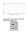
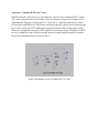
Draft the schematic shown in fig. 18. The schematic symbol for the N channel JFET is named
“njf” in the component selector in LTSpice. Note the changes from previous examples, most
importantly the flipping of voltage source V2. The JFET is a depletion mode device. Unlike
previous three terminal devices which have increasing collector or drain current with increasing
base or gate voltage, the JFET exhibits decreasing drain current with increasing gate current.
With zero volts applied to the gate a JFET conducts its maximum current. The physics of JFET
devices is outside the scope of this lab and the interested reader should consult the references
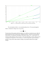
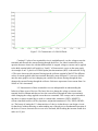
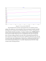
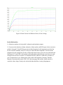
listed. The simulation results are shown in fig. 19.
Figure 18 Schematic for an N Channel JFET I-V Plot