1
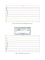
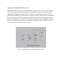
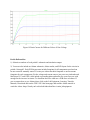
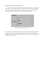
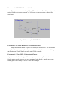
Figure 19 Drain Current for Different Values of Gate Voltage
Prelab Deliverables:
1). Submit screenshots of each prelab’s schematic and simulation output.
2). You must also include an Altium schematic, Altium netlist, and PCB layout for the circuits in
prelabs 1 through 5. Each PCB layout must include footprints for all components used and can
be auto routed or manually routed. You may use either thru-hole footprints or surface mount
footprints for each component. (For the voltage and current sources just put a two pin header and
label them VCC and GND.) Also include a grounding plane and make sure your traces are wide
enough for the increase in current. To determine the trace width use a PCB trace calculator. If
you are unsure how to use Altium please click on the Lab Equipment, Learning, Tutorials,
Manuals, Downloads link on the UNLV EE Labs homepage and read the Altium tutorial or
watch the videos. https://faculty.unlv.edu/eelabs/index.html?navi=main_labequipment