1
Appendix A. Rear Connector Pinouts
Appendix A.
Page 21
Rear Connector Pinouts
A.1. Primary XMC Connector, P5
A
B
C
D
E
F
1
PET0p0
PET0n0
3.3V
PET0p1
PET0n1
VPWR
2
GND
GND
XMC_TRST#
GND
GND
MRSTI#
3
PET0p2
PET0n2
3.3V
PET0p3
PET0n3
VPWR
4
GND
GND
XMC_TCK
GND
GND
MRSTO#
5
PET0p4
PET0n4
3.3V
PET0p5
PET0n5
VPWR
6
GND
GND
XMC_TMS
GND
GND
+12V
7
PET0p6
PET0n6
3.3V
PET0p7
PET0n7
VPWR
8
GND
GND
XMC_TDI (3)
GND
GND
-12V
9
-
-
-
-
-
VPWR
10
GND
GND
XMC_TDO (3)
GND
GND
GA0
11
PER0p0
PER0n0
MBIST#
PER0p1
PER0n1
VPWR
12
GND
GND
GA1
GND
GND
MPRESENT#
13
PER0p2
PER0n2
- (4)
PER0p3
PER0n3
VPWR
14
GND
GND
GA2
GND
GND
MSDA
15
PER0p4
PER0n4
-
PER0p5
PER0n5
VPWR
16
GND
GND
MVMRO
GND
GND
MSCL
17
PER0p6
PER0n6
-
PER0p7
PER0n7
-
18
GND
GND
-
GND
GND
-
19
REFCLK+0
REFCLK-0
-
WAKE#
ROOT0#
-
(5)
(5)
(5)
(5)
(5)
(5)
(5)
(5)
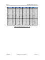
Table A.1: XMC Connector, P5
Notes:
(1) PCIe Channel 0 Lanes (3:0) are connected to the Bridge FPGA by default but can be
routed to the target FPGA.
(2) PCIe Channel 0 Lanes (7:4) are only connected to the Target FPGA. This may be used
as a second, 4-lane channel if supported by the carrier card, although this configuration
is non-standard.
(3) JTAG is unused. XMC_TDI is connected to XMC_TDO.
(4) 3.3V AUX is unused.
(5) VPWR can be either +5V or +12V.
Alpha Data
ADM-XRC-6TL User Manual
Version 1.0