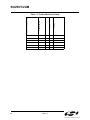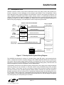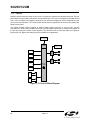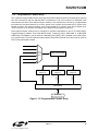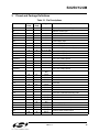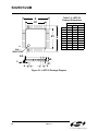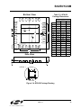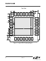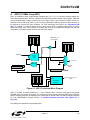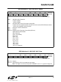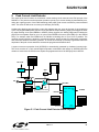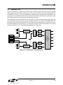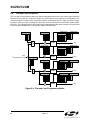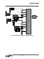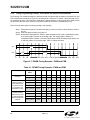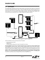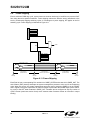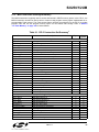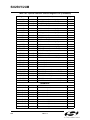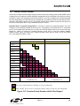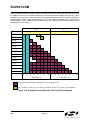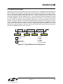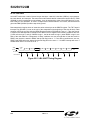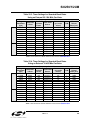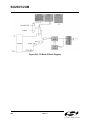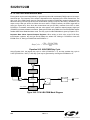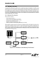
1
Si8250/1/2UM
Digital Power Controller User’s Manual
Single-Chip, Flash Digital Controller
- Supports isolated and non-isolated applications
- Supports AC/DC, DC/DC and PFC applications
- Enables new system capabilities
•
•
•
•
50 MIPS Flash System Management Processor
- 16 or 32 kB of Flash
•
-
Adaptive dead-time control
Nonlinear control response
Efficiency optimization
Self diagnostics/status reporting
•
•
Dedicated DSP-Based Control Processor
- Update rate up to 10 MHz (independent of firmware)
- Differential input ADC
- Loop filter DSP engine
•
•
-
Highly flexible DPWM with up to 6 output phases
•
•
-
PID + 2nd stage low-pass filter
Selectable discrete time or SINC 2nd stage low-pass
filter
50 kHz to greater than 1 MHz output
Less than 5 ns dithered resolution
Hardware pulse-by-pulse current limiting with programmable leading-edge blanking
Programmable hardware overcurrent protection
Typical Applications
- DC/DC converters
- AC/DC converters
- PFC circuits
- DC motor control
Packages
- 32-pin LQFP
- 28-pin 5 x 5 mm QFN
•
-
Flash can be used as EEPROM
On-board 2% oscillator
Self-sequencing, 8-channel 12-bit ADC
Supports firmware-programmable safeguards (UVLO,
OTP, OVP)
Individual hardware limit detectors with vectored
interrupts
On-board temperature sensor and VREF
High-speed, programmable general-purpose comparator
SMBus hardware interface
Enhanced UART for isolated control data link
Four 16-bit timers
3-Channel PCA for general-purpose timing or additional PWM outputs
High-current, fully-programmable I/O port lines
Comprehensive, Low-Cost Development Kit
- Minimizes learning curve and speeds
-
time-to-market
Real-time firmware kernel
•
-
greatly reduces firmware development
Intuitive compensator design tool
GUI-based waveform designer/simulator
System configuration wizards
Intuitive IDE with real-time debug
•
Standard and on-line debug modes
Temperature Range
- –40 to +125 ºC
DIGITAL PERIPHERALS
ANALOG PERIPHERALS
8-Channel
Self-Sequencing
12-Bit ADC Subsystem
2%
Oscillator
Comparator
Temp
Sensor
SMBus/
I2C
4 x 16-Bit
Timer
Port 0
UART
3-Chan
PCA
Port 1
VREF
SYSTEM MANAGEMENT PROCESSOR
16/32 K
ISP FLASH
50MIPS
8051 CPU
FLEXIBLE
VECTORED
INTERRUPTS
DEBUG
CIRCUITRY
1280B
SRAM
POR
W DT
HIGH BANDWIDTH CONTROL LOOP PROCESSOR
Diff Input
10 MHz
ADC
VREF
DAC
Rev. 0.7 8/06
DSP Filter Engine
Six-Phase
DPWM
Peak Current
Limiting & OCP
Copyright © 2006 by Silicon Laboratories
Si8250 User’s Manual
This information applies to a product under development. Its characteristics and specifications are subject to change without notice.
Si8250/1/2UM
NOTES:
2
Rev. 0.7
Si8250/1/2UM
Table of Contents
1. System Overview.................................................................................................... 19
1.1. 10 MHz Control Processor ADC ....................................................................... 21
1.2. DSP Filter Engine ............................................................................................. 22
1.3. Six-Channel DPWM .......................................................................................... 23
1.4. Peak Current Limit Comparator ........................................................................ 24
1.5. Self-Sequencing 12-Bit ADC............................................................................. 25
1.6. System Management Processor....................................................................... 26
1.7. Development Tools ........................................................................................... 27
1.8. Memory Map ..................................................................................................... 30
1.9. Comparator 0 .................................................................................................... 31
1.10.Serial Ports ....................................................................................................... 31
1.11.Port I/O ............................................................................................................ 32
1.12.Programmable Counter Array........................................................................... 33
2. System Operation................................................................................................... 35
2.1. Power Up Initialization ...................................................................................... 35
2.2. Isolated Applications ......................................................................................... 36
2.3. Non-Isolated (POL) Applications....................................................................... 37
2.4. Clock Source..................................................................................................... 37
2.5. PWM Limits, Protection and Operating Point Settings...................................... 37
3. Pinout and Package Definitions............................................................................ 39
4. ADC1 (10 MHz Loop ADC) ..................................................................................... 47
4.1. Adjustable LSB Size ......................................................................................... 48
4.2. PID Input MUX .................................................................................................. 48
4.3. Transient Detector ............................................................................................ 48
5. Peak Current Limit Detector .................................................................................. 51
5.1. Leading Edge Blanker....................................................................................... 52
5.2. Peak Current Threshold Detector ..................................................................... 52
5.3. Overcurrent Count and Compare...................................................................... 53
6. Digital PWM (DPWM) .............................................................................................. 57
6.1. Writing to the DPWM SFRs .............................................................................. 58
6.2. DPWM Input MUX............................................................................................. 58
6.3. Symmetry Lock ................................................................................................. 59
6.4. Trim and Limit Subsystem ................................................................................ 60
6.5. DPWM Timing Generator.................................................................................. 61
6.6. DPWM Bypass.................................................................................................. 66
6.7. Sync Mode ........................................................................................................ 67
6.8. Frame Skipping................................................................................................. 68
7. Rev. 0.7Voltage Reference..................................................................................... 87
8. Comparator 0 ......................................................................................................... 89
9. CIP-51 CPU.............................................................................................................. 93
9.1. Instruction Set ................................................................................................... 94
9.2. Register Descriptions........................................................................................ 99
9.3. Power Management Modes ............................................................................ 101
10. Prefetch Engine .................................................................................................... 103
Rev. 0.7
3
Si8250/1/2UM
11. Cyclic Redundancy Check Unit (CRC0) ............................................................. 105
11.1.Preparing for a CRC Calculation .................................................................... 105
11.2.Performing a CRC Calculation ....................................................................... 105
11.3.Accessing the CRC0 Result ........................................................................... 105
11.4.CRC0 Bit Reverse Feature............................................................................. 106
12. Reset Sources....................................................................................................... 109
12.1.Power-On Reset ............................................................................................. 110
12.2.Power-Fail Reset / VDD Monitor .................................................................... 111
12.3.External Reset ................................................................................................ 112
12.4.Missing Clock Detector Reset ........................................................................ 112
12.5.Comparator0 Reset ........................................................................................ 112
12.6.PCA Watchdog Timer Reset .......................................................................... 113
12.7.Flash Error Reset ........................................................................................... 113
12.8.Software Reset ............................................................................................... 113
13. Flash Memory ....................................................................................................... 115
13.1.Programming The Flash Memory ................................................................... 115
13.2.Non-volatile Data Storage .............................................................................. 117
13.3.Security Options ............................................................................................. 117
13.4.Flash Timing ................................................................................................... 120
14. External RAM ........................................................................................................ 123
15. Reference Scaling DAC (REFDAC) ..................................................................... 125
16. Memory Organization and SFRs ......................................................................... 127
16.1.Program Memory............................................................................................ 127
16.2.Data Memory .................................................................................................. 127
16.3.General Purpose Registers ............................................................................ 128
16.4.Bit Addressable Locations .............................................................................. 128
16.5.Stack .......................................................................................................... 128
16.6.Special Function Registers............................................................................. 128
16.7.Interrupt Handler............................................................................................. 136
16.8.System Management Processor Interrupt Sources and Vectors.................... 136
16.9.Interrupt Priorities ........................................................................................... 136
16.10.Interrupt Latency........................................................................................... 138
16.11.External (INT0) and ENABLE Interrupts....................................................... 138
16.12.Interrupt Register Descriptions ..................................................................... 139
17. DSP Filter Engine ................................................................................................. 147
17.1.PID Filter......................................................................................................... 147
17.2.High-Speed Low-Pass Filter (Option 1).......................................................... 150
17.3.SINC Decimation Low-Pass Filter (Option 2) ................................................. 150
17.4.Dither .......................................................................................................... 151
17.5.Output Filter Select MUX................................................................................ 151
17.6.Placing Poles and Zeros................................................................................. 151
17.7.Compensation Design Strategy...................................................................... 151
17.8.Integrator Anti-Wind Out................................................................................. 152
17.9.Integrator Clear............................................................................................... 152
4
Rev. 0.7
Si8250/1/2UM
18. ADC0 (12-Bit, Self-Sequencing ADC) ................................................................. 157
18.1.ADC0 Indirect Addressing .............................................................................. 157
18.2.Analog Multiplexer (AMUX) ............................................................................ 158
18.3.Temperature Sensor....................................................................................... 159
18.4.Output Conversion Code ................................................................................ 166
19. Port Input/Output.................................................................................................. 195
19.1.Priority Crossbar Decoder .............................................................................. 197
19.2.Port I/O Initialization ....................................................................................... 199
19.3.General Purpose Port I/O ............................................................................... 202
20. Oscillators ............................................................................................................. 207
20.1.Clock Switching .............................................................................................. 209
20.2.Low-Frequency Oscillator............................................................................... 209
20.3.Programmable Internal Oscillator ................................................................... 209
20.4.External Clock Input ....................................................................................... 209
20.5.PLL Clock Multiplier........................................................................................ 210
20.6.Reference Clock Output ................................................................................. 210
21. SMBus ................................................................................................................... 215
21.1.Supporting Documents ................................................................................... 216
21.2.SMBus Configuration...................................................................................... 216
21.3.SMBus Operation ........................................................................................... 216
21.4.Using the SMBus............................................................................................ 218
21.5.SMBus Transfer Modes.................................................................................. 226
21.6.SMBus Status Decoding................................................................................. 229
22. UART0.................................................................................................................... 233
22.1.Enhanced Baud Rate Generation................................................................... 234
22.2.Operational Modes ......................................................................................... 235
22.3.Multiprocessor Communications .................................................................... 237
23. Timers.................................................................................................................... 243
23.1.Timer 0 and Timer 1 ....................................................................................... 243
23.2.Mode 0 13-bit Counter/Timer.......................................................................... 244
23.3.Timer 2 .......................................................................................................... 252
23.4.Timer 3 .......................................................................................................... 256
24. Programmable Counter Array (PCA0) ................................................................ 261
24.1.PCA Counter/Timer ........................................................................................ 262
24.2.Watchdog Timer Mode ................................................................................... 270
24.3.Register Descriptions for PCA........................................................................ 273
25. C2 Interface ........................................................................................................... 277
25.1.C2 Interface Registers.................................................................................... 277
25.2.C2 Pin Sharing ............................................................................................... 279
Document Change List............................................................................................. 280
Contact Information.................................................................................................. 282
Rev. 0.7
5
Si8250/1/2UM
NOTES:
6
Rev. 0.7
Si8250/1/2UM
List of Figures
1. System Overview
Figure 1.1. Si8250/1/2 Block Diagram...................................................................... 19
Figure 1.2. 10 MHz Control Processor ADC ............................................................ 21
Figure 1.3. DSP Filter Engine................................................................................... 22
Figure 1.4. Six-Channel DPWM ............................................................................... 23
Figure 1.5. Peak Current Limit Comparator ............................................................. 24
Figure 1.6. Self Sequencing ADC Overview Diagram.............................................. 25
Figure 1.7. Development/In-System Debug Diagram............................................... 27
Figure 1.8. System Waveform Builder Tool.............................................................. 28
Figure 1.9. Buck Regulator Compensation Tool ...................................................... 29
Figure 1.10. Memory Map Diagram.......................................................................... 30
Figure 1.11. Comparator 0 ....................................................................................... 31
Figure 1.12. Port I/O Block Diagram......................................................................... 32
Figure 1.13. Programmable Counter Array .............................................................. 33
2. System Operation
Figure 2.1. Isolated SMPS Application..................................................................... 36
Figure 2.2. Non Isolated Converter .......................................................................... 37
3. Pinout and Package Definitions
Figure 3.1. LQFP-32 Pinout Diagram (Top View) .................................................... 40
Figure 3.2. QFN-28 Pinout Diagram (Top View) ...................................................... 41
Figure 3.3. LQFP-32 Package Diagram ................................................................... 42
Figure 3.4. QFN-28 Package Drawing ..................................................................... 43
Figure 3.5. Typical QFN-28 Landing Diagram.......................................................... 44
Figure 3.6. Typical QFN-28 Solder Paste Mask....................................................... 45
4. ADC1 (10 MHz Loop ADC)
Figure 4.1. ADC1 Functional Block Diagram............................................................ 47
5. Peak Current Limit Detector
Figure 5.1. Peak Current Limit Detector Block Diagram .......................................... 51
Figure 5.2. Leading Edge Blanker Operation ........................................................... 52
Figure 5.3. Hardware OCP Circuit Action................................................................. 53
6. Digital PWM (DPWM)
Figure 6.1. DPWM Functional Block Diagram.......................................................... 57
Figure 6.2. DPWM Input MUX.................................................................................. 58
Figure 6.3. Symmetry Lock Architecture .................................................................. 59
Figure 6.4. Trim and Limit Programming Model ....................................................... 60
Figure 6.5. DPWM Timing Generator Block Diagram .............................................. 61
Figure 6.6. DPWM Timing Register Programming Model ........................................ 63
Figure 6.7. DPWM Timing Example—PWM and PSM............................................. 64
Figure 6.8. DPWM Timing Example, Dead-time ...................................................... 65
Figure 6.9. DPWM Bypass Programming Model...................................................... 66
Figure 6.10. DPWM Sync Mode Example ................................................................ 67
Figure 6.11. Frame Skipping .................................................................................... 68
7. Rev. 0.7Voltage Reference
Figure 7.1. Voltage Reference Functional Block Diagram ....................................... 87
Rev. 0.7
7
Si8250/1/2UM
8. Comparator 0
Figure 8.1. Comparator0 Functional Block Diagram ................................................ 89
Figure 8.2. Comparator Hysteresis Plot ................................................................... 90
9. CIP-51 CPU
Figure 9.1. CIP-51 Block Diagram............................................................................ 93
10. Prefetch Engine
11. Cyclic Redundancy Check Unit (CRC0)
Figure 11.1. CRC0 Block Diagram ......................................................................... 105
Figure 11.2. Bit Reverse Register .......................................................................... 106
12. Reset Sources
Figure 12.1. Reset Sources.................................................................................... 109
Figure 12.2. Power-On and VDD Monitor Reset Timing ........................................ 110
13. Flash Memory
Figure 13.1. Flash Program Memory Map.............................................................. 117
14. External RAM
15. Reference Scaling DAC (REFDAC)
Figure 15.1. REFDAC Block Diagram .................................................................... 125
16. Memory Organization and SFRs
Figure 16.1. Memory Map ...................................................................................... 127
17. DSP Filter Engine
Figure 17.1. DSP Filter Engine Block Diagram ...................................................... 147
Figure 17.2. PID Output Sums ............................................................................... 149
Figure 17.3. Dither Control ..................................................................................... 151
Figure 17.4. Integrator Anti-Windout ...................................................................... 152
18. ADC0 (12-Bit, Self-Sequencing ADC)
Figure 18.1. ADC0 Functional Block Diagram........................................................ 157
Figure 18.2. 12-Bit ADC Auto Sequencing Detail................................................... 158
Figure 18.3. Typical Temperature Sensor Transfer Function................................. 159
Figure 18.4. ADC0 Programming Model ................................................................ 160
Figure 18.5. ADC0 Tracking Modes ....................................................................... 161
Figure 18.6. 12-Bit ADC Tracking Mode Example.................................................. 162
Figure 18.7. 12-Bit ADC Burst Mode Example with Repeat Count Set to 4 ........... 163
Figure 18.8. ADC0 Limit Detectors......................................................................... 165
Figure 18.9. Programming ADC Auto Sequencer Timeslots .................................. 166
Figure 18.10. ADC0 Equivalent Input Circuits ........................................................ 168
Figure 18.11. ADC Window Compare Examples ................................................... 169
19. Port Input/Output
Figure 19.1. Port I/O Functional Block Diagram ..................................................... 195
Figure 19.2. Port I/O Cell Block Diagram ............................................................... 196
Figure 19.3. Crossbar Priority Decoder with No Pins Skipped ............................... 197
Figure 19.4. Crossbar Priority Decoder with Crystal Pins Skipped ........................ 198
Figure 19.5. Port 0 Input Overdrive Current Range................................................ 199
20. Oscillators
Figure 20.1. Oscillator Diagram.............................................................................. 207
8
Rev. 0.7
Si8250/1/2UM
21. SMBus
Figure 21.1. SMBus Block Diagram ....................................................................... 215
Figure 21.2. Typical SMBus Configuration ............................................................. 216
Figure 21.3. SMBus Transaction ............................................................................ 217
Figure 21.4. Typical SMBus SCL Generation......................................................... 220
Figure 21.5. Typical Master Transmitter Sequence................................................ 226
Figure 21.6. Typical Master Receiver Sequence.................................................... 227
Figure 21.7. Typical Slave Receiver Sequence...................................................... 228
Figure 21.8. Typical Slave Transmitter Sequence.................................................. 229
22. UART0
Figure 22.1. UART0 Block Diagram ....................................................................... 233
Figure 22.2. UART0 Baud Rate Logic .................................................................... 234
Figure 22.3. UART Interconnect Diagram .............................................................. 235
Figure 22.4. 8-Bit UART Timing Diagram............................................................... 235
Figure 22.5. 9-Bit UART Timing Diagram............................................................... 236
Figure 22.6. UART Multi-Processor Mode Interconnect Diagram .......................... 237
23. Timers
Figure 23.1. T0 Mode 0 Block Diagram.................................................................. 245
Figure 23.2. T0 Mode 2 Block Diagram.................................................................. 246
Figure 23.3. T0 Mode 3 Block Diagram.................................................................. 247
Figure 23.4. Timer 2 16-Bit Mode Block Diagram .................................................. 252
Figure 23.5. Timer 2 8-Bit Mode Block Diagram .................................................... 253
Figure 23.6. Timer 3 16-Bit Mode Block Diagram .................................................. 256
Figure 23.7. Timer 3 8-Bit Mode Block Diagram .................................................... 257
24. Programmable Counter Array (PCA0)
Figure 24.1. PCA Block Diagram............................................................................ 261
Figure 24.2. PCA Module Block Diagram............................................................... 262
Figure 24.3. PCA Interrupt Block Diagram ............................................................. 264
Figure 24.4. PCA Capture Mode Diagram.............................................................. 264
Figure 24.5. PCA Software Timer Mode Diagram .................................................. 265
Figure 24.6. PCA High-Speed Output Mode Diagram............................................ 266
Figure 24.7. PCA Frequency Output Mode ............................................................ 267
Figure 24.8. PCA 8-Bit PWM Mode Diagram ......................................................... 268
Figure 24.9. PCA 16-Bit PWM Mode...................................................................... 269
Figure 24.10. PCA Module 5 with Watchdog Timer Enabled ................................. 270
25. C2 Interface
Figure 25.1. Typical C2 Pin Sharing....................................................................... 279
Rev. 0.7
9
Si8250/1/2UM
NOTES:
10
Rev. 0.7
Si8250/1/2UM
List of Tables
1. System Overview
Table 1.1. Product Selection Guide ......................................................................... 20
2. System Operation
Table 2.1. Si825x Power-Up State .......................................................................... 35
3. Pinout and Package Definitions
Table 3.1. Pin Descriptions ...................................................................................... 39
Table 3.2. LQFP-32 Package Dimensions .............................................................. 42
Table 3.3. QFN-28 Package Dimensions ................................................................ 43
4. ADC1 (10 MHz Loop ADC)
Table 4.1. Settings for the ADC1 Sampling Rate .................................................... 48
5. Peak Current Limit Detector
6. Digital PWM (DPWM)
Table 6.1. DPWM Timing Example—PWM and PSM ............................................. 64
Table 6.2. DPWM Timing Example, Dead-time ....................................................... 65
7. Rev. 0.7Voltage Reference
8. Comparator 0
9. CIP-51 CPU
Table 9.1. CIP-51 Instruction Set Summary ............................................................................. 95
10. Prefetch Engine
11. Cyclic Redundancy Check Unit (CRC0)
12. Reset Sources
13. Flash Memory
14. External RAM
15. Reference Scaling DAC (REFDAC)
16. Memory Organization and SFRs
Table 16.1. Special Function Register (SFR) Memory Map .................................. 129
Table 16.2. Special Function Register List ............................................................ 129
Table 16.3. Special Function Indirect Register List ............................................... 133
Table 16.4. Interrupt Summary .............................................................................. 137
17. DSP Filter Engine
Table 17.1. DSP Filter Engine Coefficients ........................................................... 149
18. ADC0 (12-Bit, Self-Sequencing ADC)
19. Port Input/Output
20. Oscillators
Table 20.1. Clock Selection Frequencies .............................................................. 208
21. SMBus
Table 21.1. SMBus Clock Source Selection .......................................................... 219
Table 21.2. Minimum SDA Setup and Hold Times ................................................ 220
Table 21.3. Sources for Hardware Changes to SMB0CN ..................................... 224
Table 21.4. SMBus Status Decoding ..................................................................... 230
22. UART0
Table 22.1. Timer Settings for Standard Baud Rates
Using the Internal Oscillator ............................................................... 240
Rev. 0.7
11
Si8250/1/2UM
Table 22.2. Timer Settings for Standard Baud Rates
Using an External 25.0 MHz Oscillator ............................................... 240
Table 22.3. Timer Settings for Standard Baud Rates
Using an External 22.1184 MHz Oscillator ......................................... 241
Table 22.4. Timer Settings for Standard Baud Rates
Using an External 18.432 MHz Oscillator ........................................... 241
Table 22.5. Timer Settings for Standard Baud Rates
Using an External 11.0592 MHz Oscillator ......................................... 242
Table 22.6. Timer Settings for Standard Baud Rates
Using an External 3.6864 MHz Oscillator ........................................... 242
23. Timers
Table 23.1. Timer Modes ....................................................................................... 243
24. Programmable Counter Array (PCA0)
Table 24.1. PCA Timebase Input Options ............................................................. 262
Table 24.2. PCA0CPM Register Settings for PCA Capture/Compare Modules .... 263
Table 24.3. Watchdog Timer Timeout Intervals1 ................................................... 272
25. C2 Interface
12
Rev. 0.7
Si8250/1/2UM
List of Registers
SFR Definition 4.1. ADC1CN: ADC1 Control . . . . . . . . . . . . . . . . . . . . . . . . . . . . . . . . 49
SFR Definition 4.2. ADC1DAT: ADC1 Data . . . . . . . . . . . . . . . . . . . . . . . . . . . . . . . . . 49
SFR Definition 4.3. TRDETCN: ADC1 Transient Detector Control . . . . . . . . . . . . . . . . 50
SFR Definition 5.1. IPKCN: Peak Current Comparator Control . . . . . . . . . . . . . . . . . . 54
SFR Definition 5.2. LEBCN: Leading-Edge Blanking Control . . . . . . . . . . . . . . . . . . . 55
SFR Definition 5.3. ICYCST: Cycle-by-Cycle Peak Current Limit Status . . . . . . . . . . 55
SFR Definition 5.4. OCPCN: Overcurrent Protection Control . . . . . . . . . . . . . . . . . . . 55
SFR Definition 6.1. DPWMOUT: Output Data . . . . . . . . . . . . . . . . . . . . . . . . . . . . . . . 69
SFR Definition 6.2. DPWMCN: DPWM Control . . . . . . . . . . . . . . . . . . . . . . . . . . . . . . 69
SFR Definition 6.3. DPWMULOCK: DPWM Symmetry Lock Control . . . . . . . . . . . . . . 69
SFR Definition 6.4. DPWMTLCD0: DPWM Trim & Limit Correction Data Register 0 . . 69
SFR Definition 6.5. DPWMTLCD1: DPWM Trim & Limit Correction Data Register 1 . . 69
SFR Definition 6.6. DPWMTLCD2: DPWM Trim & Limit Correction Data Register 2 . . 70
SFR Definition 6.7. DPWMTLCD3: DPWM Trim & Limit Correction Data Register 3 . . 70
SFR Definition 6.8. DPWMADDR: DPWM Indirect Address . . . . . . . . . . . . . . . . . . . . 70
SFR Definition 6.9. DPWMDATA: DPWM Indirect Address Data . . . . . . . . . . . . . . . . 70
SFR Definition 6.10. DPWMCN: DPWM Control . . . . . . . . . . . . . . . . . . . . . . . . . . . . . 71
SFR Definition 6.11. SW_CYC: Switching Cycle Length Control . . . . . . . . . . . . . . . . 72
SFR Definition 6.12. PH_POL: Phase Polarity Control . . . . . . . . . . . . . . . . . . . . . . . . 72
SFR Definition 6.13. ENABX_OUT: ENABX Bypass Control . . . . . . . . . . . . . . . . . . . 72
SFR Definition 6.14. OCP_OUT: Overcurrent Protection Bypass Control . . . . . . . . . . 73
SFR Definition 6.15. SWBP_OUT: Software Bypass Control . . . . . . . . . . . . . . . . . . . 73
SFR Definition 6.16. SWBP_OUTEN: Software Bypass Output Enable . . . . . . . . . . . 74
SFR Definition 6.17. PH1_CNTL0: Phase 1 Leading Edge Control Register 0 . . . . . . 75
SFR Definition 6.18. PH1_CNTL1: Phase 1 Leading Edge Control Register 1 . . . . . . 75
SFR Definition 6.19. PH1_CNTL2: Phase 1 Trailing Edge Control Register 2 . . . . . . 76
SFR Definition 6.20. PH1_CNTL3: Phase 1 Trailing Edge Control Register 3 . . . . . . 76
SFR Definition 6.21. PH2_CNTL0: Phase 2 Leading Edge Control Register 0 . . . . . . 77
SFR Definition 6.22. PH2_CNTL1: Phase 2 Leading Edge Control Register 1 . . . . . . 77
SFR Definition 6.23. PH2_CNTL2: Phase 2 Trailing Edge Control Register 2 . . . . . . 77
SFR Definition 6.24. PH2_CNTL3: Phase 2 Trailing Edge Control Register 3 . . . . . . 77
SFR Definition 6.25. PH3_CNTL0: Phase 3 Leading Edge Control Register 0 . . . . . . 78
SFR Definition 6.26. PH3_CNTL1: Phase 3 Leading Edge Control Register 1 . . . . . . 78
SFR Definition 6.27. PH3_CNTL2: Phase 3 Trailing Edge Control Register 2 . . . . . . 78
SFR Definition 6.28. PH3_CNTL3: Phase 3 Trailing Edge Control Register 3 . . . . . . 78
SFR Definition 6.29. PH4_CNTL0: Phase 4 Leading Edge Control Register 0 . . . . . . 79
SFR Definition 6.30. PH4_CNTL1: Phase 4 Leading Edge Control Register 1 . . . . . . 79
SFR Definition 6.31. PH4_CNTL2: Phase 4 Trailing Edge Control Register 2 . . . . . . 79
SFR Definition 6.32. PH4_CNTL3: Phase 4 Trailing Edge Control Register 3 . . . . . . 79
SFR Definition 6.33. PH5_CNTL0: Phase 5 Leading Edge Control Register 0 . . . . . . 80
SFR Definition 6.34. PH5_CNTL1: Phase 5 Leading Edge Control Register 1 . . . . . . 80
SFR Definition 6.35. PH5_CNTL2: Phase 5 Trailing Edge Control Register 2 . . . . . . 80
SFR Definition 6.36. PH5_CNTL3: Phase 5 Trailing Edge Control Register 3 . . . . . . 80
Rev. 0.7
13
Si8250/1/2UM
SFR Definition 6.37. PH6_CNTL0: Phase 6 Leading Edge Control Register 0 . . . . . . 81
SFR Definition 6.38. PH6_CNTL1: Phase 6 Leading Edge Control Register 1 . . . . . . 81
SFR Definition 6.39. PH6_CNTL2: Phase 6 Trailing Edge Control Register 2 . . . . . . 81
SFR Definition 6.40. PH6_CNTL3: Phase 6 Trailing Edge Control Register 3 . . . . . . 81
SFR Definition 6.41. DPWMTLLT0: Trim/Limit Low Limit Control Register 0 . . . . . . . 82
SFR Definition 6.42. DPWMTLGT0: Trim/Limit High Limit Control Register 0 . . . . . . 82
SFR Definition 6.43. DPWMTLLT1: Trim/Limit Low Limit Control Register 1 . . . . . . . 82
SFR Definition 6.44. DPWMTLGT1: Trim/Limit High Limit Control Register 1 . . . . . . 82
SFR Definition 6.45. DPWMTLLT2: Trim/Limit Low Limit Control Register 2 . . . . . . . 83
SFR Definition 6.46. DPWMTLGT2: Trim/Limit High Limit Control Register 2 . . . . . . 83
SFR Definition 6.47. DPWMTLLT3: Trim/Limit Low Limit Control Register 3 . . . . . . . 83
SFR Definition 6.48. DPWMTLGT3: Trim/Limit High Limit Control Register 3 . . . . . . 83
SFR Definition 6.49. DPWMULOCK: Symmetry Lock Control Register . . . . . . . . . . . 84
SFR Definition 6.50. DPWMTLCD0: Trim & Limit Correction Data Register 0 . . . . . . 84
SFR Definition 6.51. DPWMTLCD1: Trim & Limit Correction Data Register 1 . . . . . . 85
SFR Definition 6.52. DPWMTLCD2: Trim & Limit Correction Data Register 2 . . . . . . 85
SFR Definition 6.53. DPWMTLCD3: Trim & Limit Correction Data Register 3 . . . . . . 85
SFR Definition 6.54. DPWMOUT: DPWM Output Register . . . . . . . . . . . . . . . . . . . . 86
SFR Definition 7.1. REF0CN: Reference Control . . . . . . . . . . . . . . . . . . . . . . . . . . . . . 88
SFR Definition 8.1. CPT0CN: Comparator0 Control . . . . . . . . . . . . . . . . . . . . . . . . . . . 91
SFR Definition 8.2. CPT0MD: Comparator0 Mode Selection . . . . . . . . . . . . . . . . . . . . 92
SFR Definition 8.3. CPT0MX: Comparator0 MUX Selection . . . . . . . . . . . . . . . . . . . . 92
SFR Definition 9.1. SP: Stack Pointer . . . . . . . . . . . . . . . . . . . . . . . . . . . . . . . . . . . . . . 99
SFR Definition 9.2. DPL: Data Pointer Low Byte . . . . . . . . . . . . . . . . . . . . . . . . . . . . . 99
SFR Definition 9.3. DPH: Data Pointer High Byte . . . . . . . . . . . . . . . . . . . . . . . . . . . . . 99
SFR Definition 9.4. PSW: Program Status Word . . . . . . . . . . . . . . . . . . . . . . . . . . . . 100
SFR Definition 9.5. ACC: Accumulator . . . . . . . . . . . . . . . . . . . . . . . . . . . . . . . . . . . . 101
SFR Definition 9.6. B: B Register . . . . . . . . . . . . . . . . . . . . . . . . . . . . . . . . . . . . . . . . 101
SFR Definition 9.7. PCON: Power Control . . . . . . . . . . . . . . . . . . . . . . . . . . . . . . . . . 102
SFR Definition 10.1. PFE0CN: Prefetch Engine Control . . . . . . . . . . . . . . . . . . . . . . 103
SFR Definition 11.1. CRC0CN: CRC0 Control . . . . . . . . . . . . . . . . . . . . . . . . . . . . . . 107
SFR Definition 11.2. CRC0IN: CRC0 Data Input . . . . . . . . . . . . . . . . . . . . . . . . . . . . 108
SFR Definition 11.3. CRC0DAT: CRC0 Data Output . . . . . . . . . . . . . . . . . . . . . . . . . 108
SFR Definition 11.4. CRC0FLIP: CRC0 Bit Flip . . . . . . . . . . . . . . . . . . . . . . . . . . . . . 108
SFR Definition 12.1. VDM0CN: VDD Monitor Control . . . . . . . . . . . . . . . . . . . . . . . . 111
SFR Definition 12.2. RSTSRC: Reset Source . . . . . . . . . . . . . . . . . . . . . . . . . . . . . . 114
SFR Definition 13.1. PSCTL: Program Store R/W Control . . . . . . . . . . . . . . . . . . . . . 119
SFR Definition 13.2. FLKEY: Flash Lock and Key . . . . . . . . . . . . . . . . . . . . . . . . . . . 119
SFR Definition 13.3. FLSCL: Flash Scale . . . . . . . . . . . . . . . . . . . . . . . . . . . . . . . . . . 120
SFR Definition 13.4. ONESHOT: Flash Oneshot Period . . . . . . . . . . . . . . . . . . . . . . 121
SFR Definition 14.1. EMI0CN: External Memory Interface Control . . . . . . . . . . . . . . 123
SFR Definition 15.1. REFDAC0H: Reference DAC High Byte Data . . . . . . . . . . . . . 126
SFR Definition 15.2. REFDAC0L: Reference DAC Low Byte Data . . . . . . . . . . . . . 126
SFR Definition 15.3. REFDACMD: Reference DAC Mode Control . . . . . . . . . . . . . . 126
SFR Definition 16.1. IE: Interrupt Enable . . . . . . . . . . . . . . . . . . . . . . . . . . . . . . . . . . 139
14
Rev. 0.7
Si8250/1/2UM
SFR Definition 16.2. IP: Interrupt Priority . . . . . . . . . . . . . . . . . . . . . . . . . . . . . . . . . . 140
SFR Definition 16.3. EIE1: Extended Interrupt Enable 1 . . . . . . . . . . . . . . . . . . . . . . 141
SFR Definition 16.4. EIP1: Extended Interrupt Priority 1 . . . . . . . . . . . . . . . . . . . . . . 142
SFR Definition 16.5. EIE2: Extended Interrupt Enable 2 . . . . . . . . . . . . . . . . . . . . . . 143
SFR Definition 16.6. EIP2: Extended Interrupt Priority 2 . . . . . . . . . . . . . . . . . . . . . . 144
SFR Definition 16.7. IT01CF: INT0/ENABLE Input Configuration . . . . . . . . . . . . . . . 145
SFR Definition 17.1. PIDKPCN: PID Filter Proportional Coefficient . . . . . . . . . . . . . . 153
SFR Definition 17.2. PIDKICN: PID Filter Integration Coefficient . . . . . . . . . . . . . . . . 153
SFR Definition 17.3. PIDKDCN: PID Filter Differentiation Coefficient . . . . . . . . . . . . 153
SFR Definition 17.4. PIDA1CN: PID Low-Pass Filter Pole 1 Coefficient . . . . . . . . . . 153
SFR Definition 17.5. PIDA2CN: PID Low-Pass Filter Pole 2 Coefficient . . . . . . . . . . 154
SFR Definition 17.6. PIDA3CN: PID Low-Pass Filter Gain . . . . . . . . . . . . . . . . . . . . . 154
SFR Definition 17.7. PIDA0CN: PID SINC Filter Gain . . . . . . . . . . . . . . . . . . . . . . . . 154
SFR Definition 17.8. PIDDECCN: SINC Filter Decimation Ratio Control . . . . . . . . . . 155
SFR Definition 17.9. PIDCN: PID Filter Control . . . . . . . . . . . . . . . . . . . . . . . . . . . . . 156
SFR Definition 17.10. PIDUN: PID Output (u(n)) LSB . . . . . . . . . . . . . . . . . . . . . . . . 156
SFR Definition 18.1. ADC0MX: ADC0 Channel Select . . . . . . . . . . . . . . . . . . . . . . . . 170
SFR Definition 18.2. ADC0ADDR: ADC0 Indirect Address Pointer . . . . . . . . . . . . . . 170
SFR Definition 18.3. ADC0DATA: ADC0 Indirect Data Pointer . . . . . . . . . . . . . . . . . 171
SFR Definition 18.4. ADC0STA0: ACD0 SFR Flag Register 0 . . . . . . . . . . . . . . . . . 171
SFR Definition 18.5. ADC0STA1: ADC0 SFR Flag Register 1 . . . . . . . . . . . . . . . . . 172
SFR Definition 18.6. ADC0CF: ADC0 Configuration . . . . . . . . . . . . . . . . . . . . . . . . . 172
SFR Definition 18.7. ADC0CN: ADC0 Control . . . . . . . . . . . . . . . . . . . . . . . . . . . . . . 173
SFR Definition 18.8. ADC0TK: ADC0 Tracking Mode . . . . . . . . . . . . . . . . . . . . . . . . 174
SFR Definition 18.9. ADC0LM0: ADC0 Analog Channel Limit
Interrupt Flag Register 0 . . . . . . . . . . . . . . . . . . . . . . . . . . . . . . . 175
SFR Definition 18.10. ADC0LM1: ADC0 Analog Channel Limit
Interrupt Flag Register 1 . . . . . . . . . . . . . . . . . . . . . . . . . . . . . . . 176
SFR Definition 18.11. ADC0H: ADC0 High Byte Data . . . . . . . . . . . . . . . . . . . . . . . . 176
SFR Definition 18.12. ADC0L: ADC0 Low Byte Data . . . . . . . . . . . . . . . . . . . . . . . . 176
SFR Definition 18.13. ADC0GTH: ADC0 High Limit Detector High Byte . . . . . . . . . . 177
SFR Definition 18.14. ADC0GTL: ADC0 High Limit Detector Low Byte . . . . . . . . . . 177
SFR Definition 18.15. ADC0LTH: ADC0 Low Limit Detector High Byte . . . . . . . . . . 177
SFR Definition 18.16. ADC0LTL: ADC0 Low Limit Detector Low Byte . . . . . . . . . . . 177
SFR Definition 18.17. TS01CN: ADC0 Timeslot 0 and 1 Control . . . . . . . . . . . . . . . 178
SFR Definition 18.18. TS23CN: ADC0 Timeslot 2 and 3 Control . . . . . . . . . . . . . . . 178
SFR Definition 18.19. TS45CN: ADC0 Timeslot 4 and 5 Control . . . . . . . . . . . . . . . 178
SFR Definition 18.20. TS67CN: ADC0 Timeslot 6 and 7 Control . . . . . . . . . . . . . . . 179
SFR Definition 18.21. VSENSEH: Power Supply Output Voltage High Byte Data . . 179
SFR Definition 18.22. VSENSEL: Power Supply Output Voltage Low Byte Data . . . 179
SFR Definition 18.23. VSENSEGTH: VSENSE High Limit Detector High Byte . . . . . . 179
SFR Definition 18.24. VSENSEGTL: VSENSE High Limit Detector Low Byte . . . . . . . 180
SFR Definition 18.25. VSENSELTH: VSENSE Low Limit Detector High Byte . . . . . . . 180
SFR Definition 18.26. VSENSELTL: VSENSE Low Limit Detector Low Byte . . . . . . . 180
SFR Definition 18.27. AIN0/VINH: AIN0/Power Supply Input Voltage High Byte Data . .
Rev. 0.7
15
Si8250/1/2UM
180
SFR Definition 18.28. AIN0/VINL: AIN0/Power Supply Input Voltage Low Byte Data 181
SFR Definition 18.29. AIN0/VINGTH: AIN0/VIN High Limit Detector High Byte . . . . 181
SFR Definition 18.30. AIN0/VINGTL: AIN0/VIN High Limit Detector Low Byte . . . . . 181
SFR Definition 18.31. AIN0/VINLTH: AIN0/VIN Low Limit Detector High Byte . . . . . 181
SFR Definition 18.32. AIN0/VINLTL: AIN0/VIN Low Limit Detector Low Byte . . . . . . 182
SFR Definition 18.33. AIN1H: ADC0 MUX Channel 1 High Byte Data . . . . . . . . . . . 182
SFR Definition 18.34. AIN1L: ADC0 MUX Channel 1 Low Byte Data . . . . . . . . . . . . 182
SFR Definition 18.35. AIN1GTH: AIN1 High Limit Detector High Byte . . . . . . . . . . . 182
SFR Definition 18.36. AIN1GTL: AIN1 High Limit Detector Low Byte . . . . . . . . . . . . 183
SFR Definition 18.37. AIN1LTH: AIN1 Low Limit Detector High Byte . . . . . . . . . . . . 183
SFR Definition 18.38. AIN1LTL: AIN1 Low Limit Detector Low Byte . . . . . . . . . . . . . 183
SFR Definition 18.39. AIN2H: ADC0 MUX Channel 2 High Byte Data . . . . . . . . . . . 183
SFR Definition 18.40. AIN2L: ADC0 MUX Channel 2 Low Byte Data . . . . . . . . . . . . 184
SFR Definition 18.41. AIN2GTH: AIN2 High Limit Detector High Byte . . . . . . . . . . . 184
SFR Definition 18.42. AIN2GTL: AIN2 High Limit Detector Low Byte . . . . . . . . . . . . 184
SFR Definition 18.43. AIN2LTH: AIN2 Low Limit Detector High Byte . . . . . . . . . . . . 184
SFR Definition 18.44. AIN2LTL: AIN2 Low Limit Detector Low Byte . . . . . . . . . . . . . 185
SFR Definition 18.45. AIN3H: ADC0 MUX Channel 3 High Byte Data . . . . . . . . . . . 185
SFR Definition 18.46. AIN3L: ADC0 MUX Channel 3 Low Byte Data . . . . . . . . . . . . 185
SFR Definition 18.47. AIN3GTH: AIN3 High Limit Detector High Byte . . . . . . . . . . . 185
SFR Definition 18.48. AIN3GTL: AIN3 High Limit Detector Low Byte . . . . . . . . . . . . 186
SFR Definition 18.49. AIN3LTH: AIN3 Low Limit Detector High Byte . . . . . . . . . . . . 186
SFR Definition 18.50. AIN3LTL: AIN3 Low Limit Detector Low Byte . . . . . . . . . . . . . 186
SFR Definition 18.51. AIN4H: ADC0 MUX Channel 4 High Byte Data . . . . . . . . . . . 186
SFR Definition 18.52. AIN4L: ADC0 MUX Channel 4 Low Byte Data . . . . . . . . . . . . 187
SFR Definition 18.53. AIN4GTH: AIN4 High Limit Detector High Byte . . . . . . . . . . . 187
SFR Definition 18.54. AIN4GTL: AIN4 High Limit Detector Low Byte . . . . . . . . . . . . 187
SFR Definition 18.55. AIN4LTH: AIN4 Low Limit Detector High Byte . . . . . . . . . . . . 187
SFR Definition 18.56. AIN4LTL: AIN4 Low Limit Detector Low Byte . . . . . . . . . . . . . 188
SFR Definition 18.57. AIN5H: ADC0 MUX Channel 5 High Byte Data . . . . . . . . . . . 188
SFR Definition 18.58. AIN5L: ADC0 MUX Channel 5 Low Byte Data . . . . . . . . . . . . 188
SFR Definition 18.59. AIN5GTH: AIN5 High Limit Detector High Byte . . . . . . . . . . . 188
SFR Definition 18.60. AIN5GTL: AIN5 High Limit Detector Low Byte . . . . . . . . . . . . 189
SFR Definition 18.61. AIN5LTH: AIN5 Low Limit Detector High Byte . . . . . . . . . . . . 189
SFR Definition 18.62. AIN5LTL: AIN5 Low Limit Detector Low Byte . . . . . . . . . . . . . 189
SFR Definition 18.63. AIN6H: ADC0 MUX Channel 6 High Byte Data . . . . . . . . . . . 189
SFR Definition 18.64. AIN6L: ADC0 MUX Channel 6 Low Byte Data . . . . . . . . . . . . 190
SFR Definition 18.65. AIN6GTH: AIN6 High Limit Detector High Byte . . . . . . . . . . . 190
SFR Definition 18.66. AIN6GTL: AIN6 High Limit Detector Low Byte . . . . . . . . . . . . 190
SFR Definition 18.67. AIN6LTH: AIN6 Low Limit Detector High Byte . . . . . . . . . . . . 190
SFR Definition 18.68. AIN6LTL: AIN6 Low Limit Detector Low Byte . . . . . . . . . . . . . 191
SFR Definition 18.69. AIN7H: ADC0 MUX Channel 7 High Byte Data . . . . . . . . . . . 191
SFR Definition 18.70. AIN7L: ADC0 MUX Channel 7 Low Byte Data . . . . . . . . . . . . 191
SFR Definition 18.71. AIN7GTH: AIN7 High Limit Detector High Byte . . . . . . . . . . . 191
16
Rev. 0.7
Si8250/1/2UM
SFR Definition 18.72. AIN7GTL: AIN7 High Limit Detector Low Byte . . . . . . . . . . . . 192
SFR Definition 18.73. AIN7LTH: AIN7 Low Limit Detector High Byte . . . . . . . . . . . . 192
SFR Definition 18.74. AIN7LTL: AIN7 Low Limit Detector Low Byte . . . . . . . . . . . . . 192
SFR Definition 18.75. TEMPH: Temp Sensor High Byte Data Register . . . . . . . . . . 192
SFR Definition 18.76. TEMPL: Temp Sensor Low Byte Data Register . . . . . . . . . . . 193
SFR Definition 18.77. TEMPGTH: Temp Sensor High Limit Detector High Byte . . . 193
SFR Definition 18.78. TEMPGTL: Temp Sensor High Limit Detector Low Byte . . . . 193
SFR Definition 18.79. TEMPLTH: Temp Sensor Low Limit Detector High Byte . . . . 193
SFR Definition 18.80. TEMPLTL: Temp Sensor Low Limit Detector Low Byte . . . . . 194
SFR Definition 18.81. ADC0ASCN: ADC0 Auto Sequencing Control . . . . . . . . . . . . 194
SFR Definition 19.1. XBAR0: Port I/O Crossbar Register 0 . . . . . . . . . . . . . . . . . . . . 200
SFR Definition 19.2. XBAR1: Port I/O Crossbar Register 1 . . . . . . . . . . . . . . . . . . . . 201
SFR Definition 19.3. P0ODEN: Port0 Overdrive Mode . . . . . . . . . . . . . . . . . . . . . . . . 202
SFR Definition 19.4. P0SKIP: Port0 Skip . . . . . . . . . . . . . . . . . . . . . . . . . . . . . . . . . . 202
SFR Definition 19.5. P0MDOUT: Port0 Output Mode . . . . . . . . . . . . . . . . . . . . . . . . . 203
SFR Definition 19.6. P0: Port0 . . . . . . . . . . . . . . . . . . . . . . . . . . . . . . . . . . . . . . . . . . 203
SFR Definition 19.7. P1: Port1 . . . . . . . . . . . . . . . . . . . . . . . . . . . . . . . . . . . . . . . . . . 204
SFR Definition 19.8. P1MDOUT: Port1 Output Mode . . . . . . . . . . . . . . . . . . . . . . . . . 204
SFR Definition 19.9. P1SKIP: Port1 Skip . . . . . . . . . . . . . . . . . . . . . . . . . . . . . . . . . . 204
SFR Definition 19.10. P1MDIN: Port1 Input Mode . . . . . . . . . . . . . . . . . . . . . . . . . . . 205
SFR Definition 20.1. CLKSEL: System Clock Select . . . . . . . . . . . . . . . . . . . . . . . . . 211
SFR Definition 20.2. OSCLCN: Low-Frequency Oscillator Control . . . . . . . . . . . . . . 211
SFR Definition 20.3. OSCICN: Internal Oscillator Control . . . . . . . . . . . . . . . . . . . . . 212
SFR Definition 20.4. OSCICL: Internal Oscillator Calibration . . . . . . . . . . . . . . . . . . . 212
SFR Definition 20.5. OSCXCN: External Oscillator Control . . . . . . . . . . . . . . . . . . . . 213
SFR Definition 20.6. PLLCN: Phase-Locked Loop Control . . . . . . . . . . . . . . . . . . . . . 213
SFR Definition 21.1. SMB0CF: SMBus Clock/Configuration . . . . . . . . . . . . . . . . . . . 221
SFR Definition 21.2. SMB0CN: SMBus Control . . . . . . . . . . . . . . . . . . . . . . . . . . . . . 223
SFR Definition 21.3. SMB0DAT: SMBus Data . . . . . . . . . . . . . . . . . . . . . . . . . . . . . . 225
SFR Definition 22.1. SCON0: Serial Port 0 Control . . . . . . . . . . . . . . . . . . . . . . . . . . 238
SFR Definition 22.2. SBUF0: Serial (UART0) Port Data Buffer . . . . . . . . . . . . . . . . . 239
SFR Definition 23.1. TCON: Timer Control . . . . . . . . . . . . . . . . . . . . . . . . . . . . . . . . . 248
SFR Definition 23.2. TMOD: Timer Mode . . . . . . . . . . . . . . . . . . . . . . . . . . . . . . . . . . 249
SFR Definition 23.3. CKCON: Clock Control . . . . . . . . . . . . . . . . . . . . . . . . . . . . . . . 250
SFR Definition 23.4. TL0: Timer 0 Low Byte . . . . . . . . . . . . . . . . . . . . . . . . . . . . . . . . 251
SFR Definition 23.5. TL1: Timer 1 Low Byte . . . . . . . . . . . . . . . . . . . . . . . . . . . . . . . . 251
SFR Definition 23.6. TH0: Timer 0 High Byte . . . . . . . . . . . . . . . . . . . . . . . . . . . . . . . 251
SFR Definition 23.7. TH1: Timer 1 High Byte . . . . . . . . . . . . . . . . . . . . . . . . . . . . . . . 251
SFR Definition 23.8. TMR2CN: Timer 2 Control . . . . . . . . . . . . . . . . . . . . . . . . . . . . . 254
SFR Definition 23.9. TMR2RLL: Timer 2 Reload Register Low Byte . . . . . . . . . . . . . 255
SFR Definition 23.10. TMR2RLH: Timer 2 Reload Register High Byte . . . . . . . . . . . 255
SFR Definition 23.11. TMR2L: Timer 2 Low Byte . . . . . . . . . . . . . . . . . . . . . . . . . . . . 255
SFR Definition 23.12. TMR2H Timer 2 High Byte . . . . . . . . . . . . . . . . . . . . . . . . . . . . 255
SFR Definition 23.13. TMR3CN: Timer 3 Control . . . . . . . . . . . . . . . . . . . . . . . . . . . . 258
SFR Definition 23.14. TMR3RLL: Timer 3 Reload Register Low Byte . . . . . . . . . . . . 259
Rev. 0.7
17
Si8250/1/2UM
SFR Definition 23.15. TMR3RLH: Timer 3 Reload Register High Byte . . . . . . . . . . . 259
SFR Definition 23.16. TMR3L: Timer 3 Low Byte . . . . . . . . . . . . . . . . . . . . . . . . . . . . 259
SFR Definition 23.17. TMR3H: Timer 3 High Byte . . . . . . . . . . . . . . . . . . . . . . . . . . . 259
SFR Definition 24.1. PCA0CN: PCA Control . . . . . . . . . . . . . . . . . . . . . . . . . . . . . . . 273
SFR Definition 24.2. PCA0MD: PCA0 Mode . . . . . . . . . . . . . . . . . . . . . . . . . . . . . . . 274
SFR Definition 24.3. PCA0CPMn: PCA Capture/Compare Mode . . . . . . . . . . . . . . . 275
SFR Definition 24.4. PCA0L: PCA Counter/Timer Low Byte . . . . . . . . . . . . . . . . . . . 276
SFR Definition 24.5. PCA0H: PCA Counter/Timer High Byte . . . . . . . . . . . . . . . . . . . 276
SFR Definition 24.6. PCA0CPLn: PCA Capture Module Low Byte . . . . . . . . . . . . . . . 276
SFR Definition 24.7. PCA0CPHn: PCA Capture Module High Byte . . . . . . . . . . . . . . 276
C2 Register Definition 25.1. C2ADD: C2 Address . . . . . . . . . . . . . . . . . . . . . . . . . . . 277
C2 Register Definition 25.2. DEVICEID: C2 Device ID . . . . . . . . . . . . . . . . . . . . . . . . 277
C2 Register Definition 25.3. REVID: C2 Revision ID . . . . . . . . . . . . . . . . . . . . . . . . . 278
C2 Register Definition 25.4. FPCTL: C2 Flash Programming Control . . . . . . . . . . . . 278
C2 Register Definition 25.5. FPDAT: C2 Flash Programming Data . . . . . . . . . . . . . . 278
18
Rev. 0.7
Si8250/1/2UM
1.
System Overview
Digital power supply control offers system performance, cost, and flexibility advantages over traditional
analog approaches. Performance gains are made possible through complex adaptive and nonlinear control response and efficiency optimization algorithms. External functions can be implemented in firmware,
reducing external component count and its related size and cost. In-system programmability enables system behavior to be changed quickly and easily.
The Si8250/1/2 digital switching power supply controllers address a wide range of switch mode power
topologies. These products consist of dedicated, high-speed hardware control hardware that operates
under the supervision of an integrated Flash system management processor. As such, they offer the fast
control response, ease-of-use and economies of a hardware solution, and the flexibility of a programmable
solution.
Si8250/1/2 devices are useful in both isolated and non-isolated complex systems such as bridge and multiphase topologies. They can operate from the primary or secondary-side of the supply. They provide all
necessary system functions including analog data conversion, full digital voltage or phase angle regulation,
fault monitoring and recovery, and communications interface in a single chip. Critical control and fault
detection functions are implemented in hardware and operate autonomously, even while the CPU is disabled.
As shown in the lower portion of Figure 1.1, the cycle-by-cycle hardware control path extends from the
VSENSE input, through the 10 MHz ADC, loop filter, and six-phase DPWM. The ADC and loop filter
together generate frequency-compensated duty cycle term u(n), which directly modulates the DPWM hardware. The system management processor provides functions such as system initialization, control optimization, fault detection/recovery, system maintenance and communication interface, soft-start/stop
management, and other user-defined functions.
Interrupt
Control
I/O Port
Latches
1280B
RAM
PORT 0
Hardware
Debug
DEBUG
PORT
SMBus
3 CH PCA
I/O (8)
PORT 1
Reset Control
4x 16-bit
Timers
16/32 kB
Flash
I/O (8)
UART
MUX
SYSCLKIN
2% 25 MHz
OSC, and LFO
50MIPS 8051 CPU
System Management Processor
VDD
VSENSE
ADC
Registers &
Limit
Detectors
12-bit
200 ksps
ADC
Auto
Sequencing
Logic
8
Temp
Sensor
VSENSE
VSENSE
10 MHz
ADC
VREF
DSP
Filter Engine
VREF
DAC
Multiphase
DPWM
VREF
IPK
u(n)
Pulse-by-Pulse
Current Limiter
and OCP
Gate Control (6)
ICYC
OCP
Si8250
Figure 1.1. Si8250/1/2 Block Diagram
Rev. 0.7
19
Si8250/1/2UM
20
Product Ordering Number
Flash Memory
Number of PWM phases
UART
Package
Table 1.1. Product Selection Guide
Si8250-IQ
32 kB
6
D
LQFP-32
Si8250-IM
32 kB
6
D
QFN-28
Si8251-IQ
16 kB
6
D
LQFP-32
Si8251-IM
16 kB
6
D
QFN-28
Si8252-IQ
16 kB
3
—
LQFP-32
Si8252-IM
16 kB
3
—
QFN-28
Rev. 0.7
Si8250/1/2UM
1.1.
10 MHz Control Processor ADC
The 6-bit, 10 MHz ADC is enabled during steady-state power supply operation. It digitizes the difference
between the supply output voltage (VSENSE), and a programmable voltage reference level supplied by
the 9-bit voltage reference DAC (REFDAC). The ADC has a built-in, programmable transient detector that
asserts an interrupt when the ADC output suddenly deviates outside of the programmed range. Programmable LSB size provides a means to avoid limit cycle oscillation.
VSENSE
11:6
+
+
10 MHz
6-Bit
ADC
REFDAC
0
1
RDAC0(8:3)
VSENSE
-
+
2
To PID Filter
3
ADC Output
Data Register
RDAC0(8:0)
IN
PID Input
MUX
Transient
Detector
IRQ
Output Transient Interrupt
TRIIRQ
Figure 1.2. 10 MHz Control Processor ADC
Rev. 0.7
21
Si8250/1/2UM
1.2.
DSP Filter Engine
The DSP filter engine consists of a first-stage PID filter and second stage low-pass filter. All coefficients are
dynamically programmable enabling the system management processor to optimize loop response as load
conditions change. The PID integrator has anti-wind-out logic that is automatically enabled during peak
current limiting. One of two second-stage low-pass filters can be selected by software: a two-pole low pass
that is updated at 10 MHz or a single switching cycle "quiet mode" SINC decimation filter that generates
zeros at frequency intervals equal to fs/(2 x Decimation Ratio). The decimation ratio should be chosen to
place a zero at the PWM frequency for the maximum attenuation of the PWM frequency component.
P
a3
Windout Inhibit
From
PID Input MUX
2-Pole Low Pass Filter
I
+
Decimation SINC Filter
sum
PID
Output MUX
PIDCN:
FILTERSEL
D
PID Filter
Figure 1.3. DSP Filter Engine
22
u(n) to
DPWM
a0
Rev. 0.7
Si8250/1/2UM
1.3.
Six-Channel DPWM
The DPWM is a highly flexible timing generator that supports up to six modulation phases. Fixed or dynamically-adjustable dead times are supported. PWM and phase modulation are also supported. Output timing
resolution is 5 ns (undithered). The DPWM is initialized by the system management processor and can be
directly modulated in hardware or by the system management processor. A Trim and Limit subsystem
enables the system management processor to program u(n) upper and lower limits for each output phase.
It also provides the means for the system management processor to apply a time bias to u(n) for each timing phase to compensate for system power stage anomalies.
u0(n)
PH1
Symmetry
Lock
Logic
u1(n)
PH2
u(n)
from filter
TIMING
GENERATOR
Trim and
Limit
Symmetry
Lock
Logic
TIMING BYPASS LOGIC
u(n)
from MCU
PH3
PH4
u2(n)
PH5
u3(n)
PH6
Figure 1.4. Six-Channel DPWM
Rev. 0.7
23
Si8250/1/2UM
1.4.
Peak Current Limit Comparator
Cycle-by-cycle current limiting and overcurrent protection are provided by this subsystem. The output of
the Peak Current Limit Comparator is asserted when the inductor current waveform applied to the IPK
input exceeds the comparator threshold setting. Programmable leading edge blanking is provided to guard
against false triggers. An overcurrent protection accumulator asserts an OCP interrupt when the number of
consecutive current limit cycle interrupts equals a programmed maximum.
PH1-PH6
Phase
Selector
IPK
0 – 80 ns
Leading Edge
Blanker
+
ICYCIRQ
-
7-Bit OCP
Counter and Logic
4-bit
DAC
IPK THRESHOLD DETECTOR
IN
Figure 1.5. Peak Current Limit Comparator
24
Rev. 0.7
OUT
OCPIRQ
Si8250/1/2UM
1.5.
Self-Sequencing 12-Bit ADC
Other system parameters, such as the supply input voltage, are digitized by a self-sequencing 12-bit,
200 ksps ADC. This ADC has individual result registers with programmable limit detectors for each ADC
input MUX channel. A vectored interrupt is generated when the measured parameter exceeds the programmed limits. This monitoring mechanism enables fast response to system fault conditions and facilitates efficient interrupt-driven systems.
VSENSE
HI LIMIT
WINDOW
DETECTOR
LO LIMIT
VIN/AIN0
HI LIMIT
WINDOW
DETECTOR
LO LIMIT
AIN1
HI LIMIT
WINDOW
DETECTOR
LO LIMIT
AIN2
HI LIMIT
WINDOW
DETECTOR
LO LIMIT
AIN3
HI LIMIT
WINDOW
DETECTOR
LO LIMIT
AIN4
HI LIMIT
WINDOW
DETECTOR
LO LIMIT
AIN5
HI LIMIT
WINDOW
DETECTOR
LO LIMIT
AIN6
HI LIMIT
WINDOW
DETECTOR
LO LIMIT
AIN7
HI LIMIT
WINDOW
DETECTOR
LO LIMIT
TEMP
HI LIMIT
WINDOW
DETECTOR
LO LIMIT
TIMER 3
CNVSTR
VIN/AIN0
8 External
Inputs
AIN7
12-Bit
200 ksps
ADC
EOC
Interrupt
Temp
Sensor
SFR DEMUX
REFDAC
Output Voltage
10:1 AMUX
VSENSE
Start Conversion
TIMER 2
ADC AUTO
SEQUENCER
CHANNEL ADDRESS
DATA SFRS
VSENSEIRQ
VIN/AIN0IRQ
AIN1IRQ
AIN2IRQ
AD0IRQ
LIMIT REGISTERS
Figure 1.6. Self Sequencing ADC Overview Diagram
Rev. 0.7
25
Si8250/1/2UM
1.6.
System Management Processor
The Si8250/1/2 devices use Silicon Laboratories’ proprietary CIP-51 microcontroller core. The CIP-51 is
fully compatible with the MCS-51™ instruction set. Standard 803x/805x assemblers and compilers can be
used to develop software. The CIP-51 employs a pipelined architecture that greatly increases its instruction throughput over the standard 8051 architecture. In a standard 8051, all instructions except for MUL
and DIV take 12 or 24 system clock cycles to execute and usually have a maximum system clock of 12–
24 MHz. By contrast, the CIP-51 core executes 70% of its instructions in one or two system clock cycles,
with no instructions taking more than eight system clock cycles.
With the CIP-51's system clock running at 50 MHz, it has a peak throughput of 50 MIPS. The CIP-51 has a
total of 109 instructions. The table below shows the total number of instructions that require each execution
time.
Clocks to Execute
1
2
2/4
3
3/5
4
5
4/6
6
8
Number of Instructions
26
50
5
10
7
5
2
1
2
1
The Si8250/1/2 includes several key enhancements to the CIP-51 core and peripherals to improve performance and ease-of-use in end applications. An extended interrupt handler allows the numerous analog
and digital peripherals to operate independently of the controller core and interrupt the controller only when
necessary. By requiring less intervention from the microcontroller core, an interrupt-driven system is more
efficient and allows for easier implementation of multi-tasking, real-time systems.
Eight reset sources are available: power-on reset circuitry (POR), an on-chip VDD monitor, a watchdog
timer, a Missing Clock Detector, a voltage level detection from Comparator0, a forced software reset, an
external reset pin, and an illegal Flash access protection circuit. Each reset source except for the POR,
Reset Input Pin, or Flash error may be disabled by the user in software. The WDT may be permanently
enabled in software after a power-on reset during system management processor initialization. The internal oscillator is factory calibrated to 24.5 MHz ±2%. A clock multiplier allows for operation at up to 50 MHz.
26
Rev. 0.7
Si8250/1/2UM
1.7.
Development Tools
Si8250/1/2 devices include on-chip Silicon Laboratories 2-Wire (C2) debug circuitry that provides nonintrusive, full-speed, in-circuit debugging of the production part installed in the end application. Silicon
Labs' debugging system supports inspection and modification of memory and registers, breakpoints, and
single stepping. No additional target RAM, program memory, timers, or communications channels are
required. All the digital and analog peripherals are functional and work correctly while debugging. All the
peripherals (except for the ADC and SMBus) are stalled when the system management processor is
halted, during single stepping, or at a breakpoint in order to keep them synchronized.
Si8250/1/2 APPLICATION BUILDER
USER’s
TIMING SET
Silicon Labs IDE
TIMING BUILDER
Silicon Labs FW
SOURCE (EDITOR)
TIMING VECTORS
//----------------------------------------------------------------------------//G lobal Constants
//----------------------------------------------------------------------------#if(F330)
#define F300
0
#else
USER’s
OUTPUT
FILTER DATA
COMPENSATOR
FILTER COEFFICIENTS
#define F300
1
#define UART _ENABLE
#define THREE _CHANNEL
#endif // (F330)
0
0
sbit S 2 = P0^0;
sbit S _RESET = P0^7;
#endif // (F330)
#define TRUE
1
#define FALSE
#define CH 1
#define CH 2
#define CH 3
// CAL/SD Switch on target board
// System Reset Signal
0
0
1
2
// System Level Constants
#define SYSCLK
24500000
#define BAUDRATE
115200
SMP PARAMETER
INITIALIZER
USER’s
SYSTEM
SETTINGS
RAM AND SFR SETTINGS
UVLO = 25 V = 07FH
OVP = 1.1 V = 0F3H
MCU CONFIG
WIZARD
USER MCU
CONFIGURATION
MCU SFR SETTINGS
#define SAMPLE _RATE
15951
#define NUMCHANNELS
3
#define ADC _SAMPLERATE
48
// SYSCLK frequency (Hz)
// Baud rate of UART (bps)
// ADC0 sampling rate per channel (Hz)
// Number of channels
// ADC sampling rate (kHz)
// Define ADC Resolution and VREF
#if(F330)
#define ADC _RES
1024L
#define VREF
2430 L
#else
#define ADC _RES
256 L
#define VREF
3300L
#define ADC _SAMPLERATE
48
#else
#define ADC _RES
256 L
#define VREF
3300L
#define ADC _SAMPLERATE
48
#else
#define ADC _RES
256 L
#define VREF
3300L
#define ADC _SAMPLERATE
48
// 10-bit ADC
// ADC voltage reference (mV)
// 8-bit ADC
// ADC voltage reference (mV)
// ADC sampling rate (kHz)
// 8-bit ADC
// ADC voltage reference (mV)
// ADC sampling rate (kHz)
// 8-bit ADC
// ADC voltage reference (mV)
// ADC sampling rate (kHz)
#else
#define ADC _RES
256 L
#define VREF
3300L
#define ADC _SAMPLERATE
48
#else
#define ADC _RES
256 L
#define ADC _SAMPLERATE
48
// 10-bit ADC
#define VREF
2430L
#else
#define ADC _RES
256L
TIMER0 Enable
SMBus Port Enable
// Must be '0' for the 'F300
// Must be '0' for the 'F300
#else
// 8-bit ADC
// ADC voltage reference (mV)
// ADC sampling rate (kHz)
// 8-bit ADC
// ADC sampling rate (kHz)
#define ADC _RES
1024L
// ADC voltage reference (mV)
// 8-bit ADC
COMPILER
USER-PROVIDED
SOURCE CODE
CUSTOM FIRMWARE SOURCE CODE
ASSEMBLER/LINKER
SYSTEM
DEBUG LINK
Si8250
DEBUGGER
Figure 1.7. Development/In-System Debug Diagram
The Si8250DK development kit consists of a standard Silicon Labs IDE (editor, macro-assembler/linker,
demo C compiler and real-time, in-system debugger) and a SMPS Application Builder and real-time firmware kernel. With the power supply hardware design as a starting point, the user enters system-specific
parameters, such as minimum PWM duty cycle waveforms, system operating points, protection limits, and
system management processor configuration, into the SMPS Builder.
Compensation can be done in the familiar S-domain, allowing the user to apply proven design techniques
while fully deriving all of the benefits of a Z-domain solution. Using GUI-based design tools (examples
shown in Figure 1.8 and Figure 1.9), the user inputs his system timing, pole/zero locations, and system
parameters. With this input, the SMPS Application Builder software calculates and loads the required initialization parameters into the real-time kernel, dramatically simplifying design and speeding time-to-market. The kernel is then compiled into a downloadable firmware program and loaded into the Flash memory
of the Si8250/1/2. This development methodology minimizes the amount of code the designer must generate, lowering design risk and speeding time-to-market.
Rev. 0.7
27
Si8250/1/2UM
Figure 1.8. System Waveform Builder Tool
The System Waveform Builder Tool (Figure 1.8) generates DPWM initialization code directly from timing
waveforms drawn by the user.
28
Rev. 0.7
Si8250/1/2UM
Figure 1.9. Buck Regulator Compensation Tool
Compensation tools automatically generate filter coefficients based on the user’s system parameters and
desired pole/zero frequencies. Controller and loop magnitude and frequency plots allow the user to finetune his design.
Rev. 0.7
29
Si8250/1/2UM
1.8.
Memory Map
The CIP-51 has a standard 8051 program and data address configuration. It includes 256 bytes of data
RAM, with the upper 128 bytes dual-mapped. Indirect addressing accesses the upper 128 bytes of general
purpose RAM, and direct addressing accesses the 128 byte SFR address space. The lower 128 bytes of
RAM are accessible via direct and indirect addressing. The first 32 bytes are addressable as four banks of
general purpose registers, and the next 16 bytes can be byte addressable or bit addressable.
Program memory consists of up to 32 kB of Flash. This memory may be reprogrammed in-system in
512 byte sectors and requires no special off-chip programming voltage.
DATA MEMORY
0xFF
PROGRAM MEMORY
0x7FFF
RESERVED
0x7E00
0x7DFF
0x80
0x7F
Flash
0x3EFF
(In-System
Programmable in 512
Byte Sectors)
Si8251,
Si8252
0x20
0x1F
0x00
Bit Addressable
General Purpose
Registers
EXTERNAL DATA
ADDRESS SPACE (RAM)
0x0000
0x3FF
XRAM -1 kB
(addressable using MOVX instruction)
0x0000
Figure 1.10. Memory Map Diagram
30
Special Function
Register's
(Direct Addressing Only)
(Direct and Indirect
Addressing)
0x30
0x2F
Si8250
Upper 128 RAM
(Indirect Addressing
Only)
Rev. 0.7
Lower 128 RAM
(Direct and Indirect
Addressing)
Si8250/1/2UM
1.9.
Comparator 0
Si8250/1/2 devices include a software-configurable voltage comparator with an input multiplexer. The comparator offers programmable response time and hysteresis and two outputs that are optionally available at
the Port pins: a synchronous "latched" output (CP0) or an asynchronous "raw" output (CP0A). Comparator
interrupts may be generated on rising, falling, or both edges. When in IDLE or suspend mode, the CP0
interrupt may be used as a "wake-up" source for the processor. Comparator0 may also be configured as a
reset source.
VDD
Port I/O
Pins
Multiplexer
Interrupt
Logic
+
CP0
(Synchronous Output)
_
Synchronizer
CP0A
(Asynchronous Output)
Reset
Decision
Tree
Figure 1.11. Comparator 0
1.10. Serial Ports
The Si8250/1/2 family includes an SMBus/I2C interface and a full-duplex UART with enhanced baud rate
configuration. The UART is typically used to transmit data across the isolation barrier in isolated supplies
while the SMBus port is used as a system communication interface and can operate as a master or slave.
Each of the serial buses is fully implemented in hardware and makes extensive use of the CIP-51's interrupts, thus requiring very little CPU intervention.
Rev. 0.7
31
Si8250/1/2UM
1.11. Port I/O
Si8250/1/2 family devices include 16 port I/O pins. Port pins are organized as two byte-wide ports. The port
pins behave like typical 8051 ports with a few enhancements. Port 0 can be configured as a digital I/O and
Port 1 can be configured as a digital or analog I/O. Pins selected as digital I/O can be configured for pushpull or open-drain operation. The "weak pullups" that are fixed on typical 8051 devices may be globally disabled to save power.
The Digital Crossbar allows mapping of internal digital system resources to port I/O pins. On-chip
counter/timers, serial buses, hardware interrupts, and other digital signals can be configured to appear on
the port pins using the Crossbar control registers. This allows the user to select the exact mix of generalpurpose port I/O, digital, and analog resources needed for the application.
XBAR0, XBAR1,
PnSKIP Registers
Priority
Encoder
UART
PnMDOUT
PnMDIN Registers
P0
I/O
Cells
P0.0
P0
I/O
Cells
P1.0
P0.7
SMBus
CP0
Output
PCA
P1.7
Digital
Crossbar
T0, T1
P0
P1
Figure 1.12. Port I/O Block Diagram
32
Rev. 0.7
Si8250/1/2UM
1.12. Programmable Counter Array
The 3-channel Programmable Counter Array (PCA0) provides enhanced timer functionality while requiring
less CPU intervention than the standard 8051 counter/timers. The PCA consists of a dedicated 16-bit
counter/timer and three 16-bit capture/compare modules. The counter/timer is driven by a programmable
time base that can select between six sources: system clock, system clock divided by four, system clock
divided by twelve, the external oscillator clock source divided by 8, real-time clock source divided by 8,
Timer 0 overflow, or an external clock signal on the External Clock input (ECI) input pin.
Each capture/compare module may be configured to operate independently in one of six modes: EdgeTriggered Capture, Software Timer, High-Speed Output, Frequency Output, 8-Bit PWM, or 16-Bit PWM.
Additionally, PCA Module 2 may be used as a watchdog timer (WDT), and is enabled in this mode following a system reset. The PCA Capture/Compare Module I/O and the External Clock Input may be routed to
Port I/O using the digital crossbar.
SYSCLK/2
SYSCLK/4
TMR0 Overflow
ECI
PCA
CLOCK
MUX
16-Bit Counter/Timer
SYSCLK
EXT CLK/8
Capture/Compare
Module 0
Capture/Compare
Module 1
Capture/Compare
Module 2
CEX2
CEX1
CEX0
CROSSBAR
PORT I/O
Figure 1.13. Programmable Counter Array
Rev. 0.7
33
Si8250/1/2UM
NOTES:
34
Rev. 0.7
Si8250/1/2UM
2.
System Operation
2.1.
Power Up Initialization
When reset, the Si8250 enters lockout mode (minimum current consumption state) as specified in
Table 2.1. During power up, all I/O pins of the Si8250/1/2 are at high impedance (except PH1–PH6, which
are low) until device hardware is in its starting state. When this occurs, the I/O pins transition to the user's
programmed states. The PH1–PH6 outputs remain low until either initialized to some other state by the
system management processor or until DPWM switching begins. The system management processor is
enabled and operating at 80 kHz. Typically, the system management processor will remain enabled long
enough for firmware to initialize operating parameters, then will enter Stop mode if VIN is below the UVLO
threshold. The system management processor can be restored to operating mode by any of four wake-up
sources: a Comparator0 interrupt; the falling edge of the UART RX input (for isolated applications); a
VIN0/VIN level interrupt (non-isolated applications), or a system management processor reset.
Table 2.1. Si825x Power-Up State
Si8250 Peripheral
Power-Up State
VREF Generator
Disabled
Reference Scaling DAC
Disabled, output = 0 V
10 MHz ADC (ADC1)
Disabled
ADC0 Input MUX
Channel 1 (ADC0) selected
DSP Filter
Disabled
DPWM Input Control MUX
Channel 0 (filter output) selected
DPWM
Disabled, PH outputs = 00
Leading Edge Blanker
Disabled
Blanker VT DAC
Disabled
Current Limit Comparator
Disabled
OCP Detector
Disabled
ADC0
Disabled
Port 0 I/O
All I/O = input mode, open drain configuration
Port 1 I/O
All I/O = input mode, open drain configuration
Interrupts
Individually and globally disabled
POR/Brown-out detector
Enabled
System Management Processor Clock
80 kHz LFO enabled
GP Comparator
Disabled
Serial Ports and Timers
Disabled
Rev. 0.7
35
Si8250/1/2UM
2.2.
Isolated Applications
An isolated supply example is shown in Figure 2.1. Critical primary-side voltages (e.g., VIN) are digitized
and transmitted to the UART on-board the Si8250/1/2 by a Silicon Labs C8051F30x MCU. All secondaryside voltages are measured and converted directly by the ADC0 on the Si8250/1/2. Primary-side gate control signals are isolated using a Silicon Labs Si840x quad-channel, high-speed isolator. Secondary side
gate control lines connect directly to the inputs of the corresponding external driver ICs.
PRIMARY-SIDE
POWER STAGES,
DRIVERS AND PEAK
CURRENT SENSING
VIN
SECONDARY-SIDE
POWER STAGES,
DRIVERS AND
OUTPUT FILTER
VOUT
Si8250
PH3
VSENSE
PH4
(ISOLATED)
ICYC
C8051F30x
I/O
AIN0
PH1
DIGITAL
ISOLATOR
I/O
Other analog
and digital
primary-side I/O
RX
PH2
Other analog and digital
secondary-side I/O
I/O
TX
TX
RX
I/O
ISOLATED AUX SUPPLY
VDD
Figure 2.1. Isolated SMPS Application
36
Rev. 0.7
GND
Si8250/1/2UM
2.3.
Non-Isolated (POL) Applications
The non-isolated application differs from the isolated case in that the UART is not used. In the non-isolated
case, the VIN/AIN0 channel of the 12-bit ADC connects directly to the VIN/AIN0 input of ADC0 as shown in
Figure 2.2. A local regulator biases the Si8250/1/2 and all gate control signals connect directly to the external MOSFET driver ICs.
POWER STAGES,
DRIVERS, PEAK CURRENT SENSING AND
OUTPUT FILTER
VIN
VOUT
Si8250
PH3
PH4
ICYC
I/O
Other analog and digital
secondary-side I/O
PH1
I/O
PH2
VIN/AIN0
LOCAL
VREG
VDD
GND
Figure 2.2. Non Isolated Converter
2.4.
Clock Source
The Si8250/1/2 is clocked internally from the low-frequency oscillator (LFO), 25 MHz oscillator, or external
clock source. A SYNC function is provided to synchronize the Si8250/1/2 and external hardware.
2.5.
PWM Limits, Protection and Operating Point Settings
The minimum and maximum PWM duty cycle limits are programmed in firmware and loaded into hardware
registers during by the system management processor during initialization. The PWM duty cycle increases
in a linear fashion from programmed minimum to programmed maximum as u(n) varies from zero to full
scale (0x1FF). System safeguard settings (e.g., over-voltage protection threshold) and operating point settings (e.g., output voltage) are also firmware-programmable and loaded to hardware registers during initialization.
Rev. 0.7
37
Si8250/1/2UM
NOTES:
38
Rev. 0.7
Si8250/1/2UM
3.
Pinout and Package Definitions
Table 3.1. Pin Descriptions
Name
QFN-28 LQFP-32
Pin #
Pin#
Type
Description
RST/C2CK
1
1
D I/O
IPK
2
2
AIN
Inductor current input
VSENSE
3
3
AIN
Output voltage feedback input
GND
4
—
AIN
Ground
GNDA
—
4
AIN
Ground
VDD
5
—
AIN
Power supply input
VDDA
—
5
AIN
Power supply input
VREF
6
6
AIN
External voltage reference input
P1.0/VIN or AIN0
7
7
D I/O or AIN
Port 1 I/O or scaled power supply input voltage
P1.1/AIN1
8
8
D I/O or AIN
Port 1 I/O or ADC input 1
Reset input or bidirect debug clock
P1.2/AIN2
9
9
D I/O or AIN
Port 1 I/O or ADC input 2
P1.3/AIN3
10
10
D I/O or AIN
Port 1 I/O or ADC input 3
P1.4/AIN4
11
11
D I/O or AIN
Port 1 I/O or ADC input 4
GND
—
12
AIN
Ground
VDD
—
13
AIN
Power supply input
P1.5/AIN5
12
14
D I/O or AIN
P1.6/AIN6
13
15
D I/O or AIN
P1.7/ AIN7/C2D
14
16
P0.7
15
17
P0.6
16
18
P0.5
17
19
D I/O
Port 0 I/O
P0.4
18
20
D I/O
Port 0 I/O
P0.3/XCLK
19
21
D I/O
Port 0 I/O
P0.2
20
22
D I/O
Port 0 I/O
P0.1
21
23
D I/O
Port 0 I/O
P0.0
22
24
D I/O
Port 0 I/O or bidirectional debug data
PH6
23
25
DOUT
Phase 6 switch control output
PH5
24
26
DOUT
Phase 5 switch control output
PH4
25
27
DOUT
Phase 4 switch control output
VDD
—
28
AIN
Power supply input
GND
—
29
AIN
Ground
PH3
26
30
DOUT
Phase 3 switch control output
PH2
27
31
DOUT
Phase 2 switch control output
PH1
28
32
DOUT
Phase 1 switch control output
Port 1 I/O or ADC input 5
Port 1 I/O or ADC input 6
D I/O, DIN or Port 1 I/O or ADC input 7 or C2 Data
AIN
D I/O
Port 0 I/O
D I/O
Port 0 I/O
Rev. 0.7
39
PH1
PH2
PH3
GND
VDD
PH4
PH5
PH6
32
31
30
29
28
27
26
25
Si8250/1/2UM
RST/C2CK
1
24
P0.0
IPK
2
23
P0.1
VSENSE
3
22
P0.2
GNDA
4
21
P0.3 / XCLK
VDDA
5
20
P0.4
VREF
6
19
P0.5
P1.0/VIN/AIN0
7
18
P0.6
P1.1/AIN1
8
17
P0.7
13
14
15
16
VDD
P1.5/AIN5
P1.6/AIN6
P1.7/AIN7/C2D
11
P1.4/AIN4
12
10
P1.3/AIN3
GND
9
P1.2/AIN2
Si8250/1/2
Top View
Figure 3.1. LQFP-32 Pinout Diagram (Top View)
40
Rev. 0.7
PH1
PH2
PH3
PH4
PH5
PH6
P0.0
27
26
25
24
23
22
GND
28
Si8250/1/2UM
RST / C2CK
1
21
P0.1
IPK
2
20
P0.2
VSENSE
3
19
P0.3/XCLK
GND
4
18
P0.4
VDD
5
17
P0.5
VREF
6
16
P0.6
P1.0/VIN/AIN0
7
15
P0.7
Si8250/1/2
Top View
12
13
14
P1.5/AIN5
P1.6/AIN6
P1.7/AIN7/C2D
10
P1.3/AIN3
11
9
P1.2/AIN2
P1.4/AIN4
8
P1.1/AIN1
GND
Figure 3.2. QFN-28 Pinout Diagram (Top View)
Rev. 0.7
41
Si8250/1/2UM
Table 3.2. LQFP-32
Package Dimensions
D
D1
E1 E
32
PIN 1
IDENTIFIER
A
A1
A2
b
D
D1
e
E
E1
L
1
A2
A
L
b
A1
e
Figure 3.3. LQFP-32 Package Diagram
42
Rev. 0.7
MIN
—
0.05
1.35
0.30
—
—
—
—
—
0.45
MM
TYP
—
—
1.40
0.37
9.00
7.00
0.80
9.00
7.00
0.60
MAX
1.60
0.15
1.45
0.45
—
—
—
—
—
0.75
Si8250/1/2UM
Table 3.3. QFN-28
Package Dimensions
14
13
12
11
10
9
8
Bottom View
L
7
15
16
D2
17
D2
2
e
4
19
E2
2
3
18
R
20
2
21
22
23
24
25
26
27
DETAIL 1
28
1
6xe
E
5
E2
b
6
6xe
D
MAX
1.00
0.05
1.00
—
0.30
—
3.35
—
3.35
—
0.65
—
—
—
—
—
—
—
—
A1
e
A3
MM
TYP
0.90
0.02
0.65
0.25
0.23
5.00
3.15
5.00
3.15
0.5
0.55
28
7
7
—
0.435
0.435
0.18
0.18
A
A2
Side View
A
A1
A2
A3
b
D
D2
E
E2
e
L
N
ND
NE
R
AA
BB
CC
DD
MIN
0.80
0
0
—
0.18
—
2.90
—
2.90
—
0.45
—
—
—
0.09
—
—
—
—
DETAIL 1
CC
DD
BB
AA
Figure 3.4. QFN-28 Package Drawing
Rev. 0.7
43
Si8250/1/2UM
0.30 mm
0.35 mm
0.50 mm
0.10 mm
0.85 mm
0.50 mm
0.20 mm
0.20 mm
0.50 mm
Top View
b
0.20 mm
L
e
E2
0.20 mm
0.30 mm
0.50 mm
0.85 mm
0.35 mm
0.10 mm
E
Figure 3.5. Typical QFN-28 Landing Diagram
44
Rev. 0.7
D
D2
Optional
GND
Connection
Si8250/1/2UM
0.30 mm
0.50 mm
0.85 mm
0.35 mm
0.50 mm
0.60 mm
0.20 mm
0.10 mm
0.20 mm
0.20 mm
0.50 mm
Top View
0.60 mm
0.30 mm
0.70 mm
b
0.20 mm
D
D2
0.40 mm
e
L
E2
0.20 mm
0.30 mm
0.50 mm
0.85 mm
0.35 mm
0.10 mm
E
Figure 3.6. Typical QFN-28 Solder Paste Mask
Rev. 0.7
45
Si8250/1/2UM
NOTES:
46
Rev. 0.7
Si8250/1/2UM
4.
ADC1 (10 MHz Loop ADC)
ADC1 is a differential input, programmable sampling rate (10, 5, 2.5, or 1.25 MHz) analog-to-digital converter with programmable LSB size. It digitizes the difference between sensed output voltage, VSENSE,
and the programmable voltage reference into a 6-bit signed value. The resolution of ADC1 can be programmed over an LSB range from 4 to 20 mV. The programmable LSB size allows the ADC resolution to
be adjusted to prevent limit cycle oscillation. For more information, see Section “4.1. Adjustable LSB
Size” on page 48. To minimize power during Lockout mode, ADC1 is disabled when power is initially
applied and when reset. Once enabled, it continuously converts at programmed sampling rate with the
converted 2’s complement result stored in the ADC1DAT register.
VSENSE[11:6]
(from ADC0)
RES3
RES2
RES1
RES0
PIDCN
VSENSE
+
-
+
RDAC0[8:3]
+
PIDINSEL1
PIDINSEL0
ADC1EN
EOC1IRQ
reserved
ADC1CN
10 MHz
6-Bit
ADC
00
01
To PID Filter
10
11
REFDAC
REFDAC0H
REFDAC0L
PID Input
MUX
ADC1DAT
SFR Bus
READ/WRITE
TRDETEN
TRIIRQ
TRAN5
TRAN4
TRAN3
TRAN2
TRAN1
TRAN0
TRDETCN
IN
THRES
Output Transient Interrupt
TRIIRQ
Transient
Detector
Figure 4.1. ADC1 Functional Block Diagram
ADC1 is enabled by setting ADCEN to ‘1’. Once enabled, ADC1 converts continuously and asserts
EOCIRQ at the end of each conversion. The resolution of ADC1 is programmed by RES[3:0] in ADC1CN,
and the sampling frequency is selected by the combination of ADCSP1 bit in PLLCN<2> and the ADCSP2
bit in the PIDDECCN<7> register (Section “17.3. SINC Decimation Low-Pass Filter (Option 2)” on
page 150).
The settings are described in the following table.
Rev. 0.7
47
Si8250/1/2UM
Table 4.1. Settings for the ADC1 Sampling Rate
4.1.
Bit ADCSP1 in Register
PLLCN<2>
Bit ADCSP2 in Register
PIDDECCN<7>
ADC1 Sampling Rate
0
0
10 MHz
1
0
5 MHz
0
1
2.5 MHz
1
1
1.25 MHz
Adjustable LSB Size
Limit cycle oscillation produces unwanted tones in the power supply output frequency spectrum. It is typically caused by the lack of an integration term in the compensator, and/or too coarse a DPWM resolution
relative to that of the ADC. The Si8250/1/2 family offers two ways to address limit cycle oscillation:
• Adjust ADC1 LSB size: This action changes the voltage threshold between adjacent ADC output
states. The ADC LSB size is adjusted to be larger than the DPWM LSB size. This allows the DPWM
LSB to fit within the zero bin of the ADC, eliminating the possibility of limit cycle oscillation.
• Controlled dither: The DPWM effective resolution can be increased by dithering using the on-board
pseudo-random noise source. See Section “17. DSP Filter Engine” on page 147 for more details.
4.2.
PID Input MUX
The PIDINSEL bits in the PIDCN register control the address selection for the PID input MUX. This MUX
provides the means for the system management processor to route one of four different inputs to the PID
filter:
• Channel 0: The output of ADC1.
• Channel 1: The difference between VSENSE (as measured by ADC0) and REFDAC input data.
• Channel 2: Ground.
• Channel 3: The difference between VSENSE and the reference setting as calculated by the system
management processor. This feature supports PFC applications where the system management processor performs phase angle control, and the 10 MHz hardware loop of the Si8250 provides boost regulator control.
The PID input MUX typically operates in Channel 0 mode during steady-state operation. When the PID
input MUX is set to address 0, ADC1 is selected and ADC1DAT acts as a read-only register. Channel 1 is
selected during soft-start because the 12-bit resolution provided by ADC0 results in small step sizes during
the soft-start ramp. MUX Channel 2 mode is provided to facilitate system debug. MUX Channel 3 mode the
ADC1DAT register acts as a read/write register, providing the means for the system management processor calculate and write the difference term directly into the control loop to support low control bandwidth
applications such as power factor correction. In this mode, ADC1DAT becomes a read/write register.
4.3.
Transient Detector
Due to the high dc gain provided by the PID filter integrator term, the output of ADC1 typically deviates by
±1 LSB during normal system operation. A sudden voltage transient forces ADC1 output beyond this range
due to the relatively slower response of the filter. The Transient Detector monitors the output of ADC1 and
asserts a TRIIRQ interrupt when the output of ADC1 exceeds a user-specified range. The Transient Detector is enabled when the TRDETEN bit in the TRDETCN register is set to 1. The TRIIRQ interrupt is
asserted when the absolute value of ADC1 output exceeds the limits programmed by TRAN[4:0] in the
TRDETCN register. The typical response to a transient detector interrupt is an increase to the loop gain as
outlined in Section “17. DSP Filter Engine” on page 147.
48
Rev. 0.7
Si8250/1/2UM
SFR Definition 4.1. ADC1CN: ADC1 Control
R/W
R
—
—
R/W
R/W
R/W
R/W
Reset Value
—
RES3
RES2
RES1
RES0
00000000
Bit 4
Bit 3
Bit 2
Bit 1
Bit 0
ADC1EN EOC1IRQ reserved
Bit 7
Bit 6
Bit 5
SFR Address: 0xFE
Bit 7:
ADC1EN: ADC1 Enable Bit
0: ADC1 disabled.
1: ADC1 enabled.
Bit 6
EOC1IRQ: ADC1 End-of-Conversion Interrupt Bit
0: ADC1 has not completed a data conversion since the last time EOC1IRQ was cleared.
1: ADC1 has completed a data conversion.
Bit 5
Reserved, must be maintained ‘0’.
Bit 4
Unused.
Bits 3–0: RES[3:0]: ADC1 Resolution Control Bits (LSB size)
0000: Resistor ladder disable
0001: Reserved
0010: 4 mV (default)
0011: 6 mV
0100: 8 mV
0101: 10 mV
0110: 12 mV
0111: 14 mV
1000: 16 mV
1001: 18 mV
1010: 20 mV
1011–1111: Reserved
SFR Definition 4.2. ADC1DAT: ADC1 Data
—
—
—
—
Bit 7
Bit 6
R/W
R/W
R/W
R/W
R/W
R/W
Bit 5
Bit 4
Bit 3
Bit 2
Bit 1
Bit 0
Reset Value
00000000
SFR Address: 0xFD
Bits 7–6: Unused.
Bits 5–0: ADC1DAT[5:0]: ADC1 2s complement output data.
Note: This register is read-only except when PIDINSEL is set to ‘11’ (system management
Rev. 0.7
49
Si8250/1/2UM
SFR Definition 4.3. TRDETCN: ADC1 Transient Detector Control
R/W
R/W
TRDETEN TRIIRQ
Bit 7
Bit 6
—
R/W
R/W
R/W
R/W
R/W
Reset Value
—
TRAN4
TRAN3
TRAN2
TRAN1
TRAN0
00011111
Bit 5
Bit 4
Bit 3
Bit 2
Bit 1
Bit 0
SFR Address: 0x3D
Bit 7:
TRDETEN: PID Input Transient Detector Enable Bit
0: Transient detector disabled.
1: Transient detector enabled.
Bit 6:
TRIIRQ: Transient Detector Interrupt Flag
0: No transient detected.
1: Transient detected.
Bit 5:
Not used.
Bits 4–0: TRAN[4:0]: Transient Magnitude Detector Threshold
These bits set the magnitude of the change on the output of ADC1 that will trigger a transient interrupt (TRIIRQ). For example, if TRAN[4:0] = 00110b, TRIIRQ will be asserted for
all positive ADC1 output values at or greater than 000110b or less than 111010b.
50
Rev. 0.7
Si8250/1/2UM
5.
Peak Current Limit Detector
The output of the user's inductor or transformer current-sensing circuit connects to the IPK input pin of the
Si8250/1/2. The peak current limit detector provides cycle-by-cycle current limiting by automatically truncating the ongoing portion of the PWM switching phase when peak current exceeds a preset threshold
value. This event is defined as a current cycle interrupt (ICYCIRQ).
Leading edge blanking prevents false current limit triggers that may occur at the start of each switching
cycle. The programmable phase selector circuit specifies the output switching edge(s) that trigger the leading edge blanking circuit (bits LEBPHn in LEBCN). When triggered, the leading edge blanker inhibits the
peak current comparator input for up to 16 cycles of the DPWM clock source (bits LEB[1:0] in the LEBCN
SFR). For example, when the DPWM clock is 200 MHz a blanking time of up to 80 ns is possible. The
resulting current waveform is applied to a threshold detector, which consists of a high-speed comparator
and 4-bit DAC threshold reference generator. A current limit interrupt (ICYCIRQ) is generated when the
amplitude of the peak current waveform exceeds the programmed threshold value.
A system overcurrent protection fault (OCPIRQ) is automatically generated by dedicated counting logic.
This circuit consists of a 7-bit counter/digital comparator combination that asserts an OCPIRQ when the
number of consecutive ICYCIRQ events equals the programmed limit of the OCP[6:0] bits in OCPCN.
Phase
Selector
PWMCLK
VDD
EOFIRQ
0–80 ns
Leading Edge
Blanker
IPK
HYST1
HYST0
IPKCN
IPKCMPEN
PH1–PH6
LEBTM1
LEBTM0
LEBPH6
LEBPH5
LEBPH4
LEBPH3
LEBPH2
LEBPH1
LEBCN
+
ICYCIRQ
VT3
VT2
VT1
VT0
7-Bit OCP
Counter and Logic
4-bit
DAC
IN
IPK THRESHOLD DETECTOR
EOFIRQ
OUT
OCPIRQ
CLEAR
ICYCST
ICYCIRQ
PHnT6
PHnT5
PHnT4
PHnT3
PHnT2
PHnT1
PHnT0
OCPCN
OCPIRQ
OCP6
OCP5
OCP4
OCP3
OCP2
OCP1
OCP0
IPKCN
-
LIMIT
OCP
COUNT
Figure 5.1. Peak Current Limit Detector Block Diagram
Rev. 0.7
51
Si8250/1/2UM
5.1.
Leading Edge Blanker
The leading-edge blanking circuit inhibits the peak current threshold detector for a fixed time period
(tBLANK) determined by the settings in LEBCN. Blanking is triggered on the rising edge of the PHn outputs
specified by bits LEBPH1–LEBPH6 in LEBCN. Any combination of PHn outputs may be designated as triggers by setting the corresponding LEBPH1-LEBPHn bit to 1. The blanking time is programmed by
LEBTM0, LEBTM1 in LEBCN. (See Section “SFR Definition 5.2. LEBCN: Leading-Edge Blanking Control” on page 55 for programming details.) As shown in Figure 5.2, the peak current detector input is shutoff for tBLANK when triggered by the states of LEBPH1–LEBPH6.
LEBTM1
LEBTM0
LEBPH6
LEBPH5
LEBPH4
LEBPH3
LEBPH2
LEBPH1
LEBCN
PHn
Phase
Selector
IPK DETECTOR
INPUT INHIBITED
(tBLANK)
PH1-PH6
IPK DETECTOR
INPUT ENABLED
Peak Current
Comparator
IPK
0–80 ns
Leading Edge
Blanker
+
-
Figure 5.2. Leading Edge Blanker Operation
5.2.
Peak Current Threshold Detector
The peak current detector consists of a 12 ns comparator with programmable hysteresis and a 4-bit DAC
to set the threshold. Detector hysteresis is programmable from 0 mV to 20 mV in 5 mV steps. The peak
current detector threshold is programmable from 50 to 800 mV in 50 mV increments.
52
Rev. 0.7
Si8250/1/2UM
5.3.
Overcurrent Count and Compare
The overcurrent count and compare logic consists of 7-bit counting hardware and a digital comparator that
compares the number of consecutive current limit cycles (ICYCIRQ) to a user-programmed maximum; an
OCP interrupt is issued when the programmed count limit is reached. The count limit is programmed in
overcurrent protection control SFR (OCPCN). In addition, the current number of consecutive current limit
cycles can be read by the system management processor at any time in the Cycle Status SFR (ICYCST).
The ICYCIRQ cycle counter is reset to zero by hardware when a normal (non-current-limit) cycle occurs.
For example, OCP[6:0] = 0001111b will result in an OCPIRQ being asserted on the 16th consecutive ICYCIRQ event. If a switching cycle is completed through the voltage feedback path (i.e., a normal, "non-current limit" cycle), the OCP count is immediately reset to zero. There must be 16 current limit cycles in a row
for an OCPIRQ to be asserted in this example. If the OCP count reaches the user-programmed limit, the
OCP count is reset, and the DPWM bypass is initiated if enabled. For more information, see Section
“6.6. DPWM Bypass” on page 66.
A graphical example of OCP detector action is shown in Figure 5.3. In this example, there are two phases
per switching cycle. The OCP detector is programmed to assert the OCPIRQ when six consecutive current
limit events occur. As shown, the peak current detector asserts ICYCIRQ each time peak current exceeds
the threshold. At first, there are three consecutive ICYCIRQs, followed by a non-current-limit cycle (i.e.,
normal loop action), which causes the ICYCIRQ count to be cleared at the end of the normal cycle. The
accumulation of ICYCIRQ events resumes when peak current is again above the detector threshold setting, and OCPIRQ is asserted at the completion of the sixth ICYCIRQ. The EOF interrupt is asserted by
hardware at the end of each switching cycle and is shown here for reference only.
Note: The OCP hardware shutdown may be disabled by setting HWBP in the DPWMCN to 0.
PH
Outputs
PHn
PHn
PHn
PHn
PHn
PHn
PHn
PHn
1
2
PHn
PHn
PHn
PHn
Outputs =
OCP Bypass
EOF
Interrupt
Threshold
IPK
Input
ICYCIRQ
ICYC Count
1
2
3
0
3
4
5
6
DCP IRQ Asserted
OCPIRQ
Figure 5.3. Hardware OCP Circuit Action
Rev. 0.7
53
Si8250/1/2UM
SFR Definition 5.1. IPKCN: Peak Current Comparator Control
R/W
R/W
R/W
R/W
R/W
R/W
R/W
R/W
Reset Value
IPKEN
ICYCIRQ
VT3
VT2
VT1
VT0
HYST1
HYST0
00000000
Bit 7
Bit 6
Bit 5
Bit 4
Bit 3
Bit 2
Bit 1
Bit 0
SFR Address: 0xA0
Bit 7:
IPKEN: Peak Current Comparator Enable Bit
0: Peak current comparator disabled
1: Peak current comparator enabled
Bit 6:
ICYCIRQ: Peak Current Comparator Interrupt Output
0: Normal operation—no cycle current limit in progress
1: Current limit cycle in progress
Bits 5–2: VT[3:0]: Peak Current Comparator Voltage Threshold Control
0000: 50 mV
0001: 100 mV
0010: 150 mV
0011: 200 mV (default)
0100: 250 mV
0101: 300 mV
0110: 350 mV
0111: 400 mV
1000: 450 mV
1001: 500 mV
1010: 550 mV
1011: 600 mV
1100: 650 mV
1101: 700 mV
1110: 750 mV
1111: 800 mV
Bits 1–0: HYST[1:0]: Peak Comparator Hysteresis Control Bits
00: 0 mV
01: 5 mV
10: 10 mV
11: 20 mV
54
Rev. 0.7
Si8250/1/2UM
SFR Definition 5.2. LEBCN: Leading-Edge Blanking Control
R/W
R/W
R/W
R/W
R/W
R/W
R/W
LEBTM1
LEBTM0
LEBPH6
LEBPH5
LEBPH4
LEBPH3
LEBPH2
Bit 7
Bit 6
Bit 5
Bit 4
Bit 3
Bit 2
Bit 1
R/W
Reset Value
LEBPH1 00000000
Bit 0
SFR Address: 0xD6
Bits 7–6: LEBTM[1:0]: Leading-Edge Blanking Period
00: 0 cycles of the DPWM clock (i.e., 0 ns blanking time)
01: 4 cycles of the DPWM clock (i.e., 20 ns blanking time at 200 MHz)
10: 8 cycles of the DPWM clock (i.e., 40 ns blanking time at 200 MHz)
11: 16 cycles of the DPWM clock (i.e., 80 ns blanking time at 200 MHz)
Bits 5–0: LEBPHn: Leading-Edge Blanking Phase Select
0: The leading edge of phase n is passed through with no leading-edge blanking added.
1: The leading edge of phase n is blanked for the time period specified by the LEBTM[1:0]
bits.
SFR Definition 5.3. ICYCST: Cycle-by-Cycle Peak Current Limit Status
R
R
R
R
R
R
R
R
Reset Value
reserved ICYCCNT6 ICYCCNT5 ICYCCNT4 ICYCCNT3 ICYCCNT2 ICYCCNT1 ICYCCNT0 00000000
Bit 7
Bit 6
Bit 5
Bit 4
Bit 3
Bit 2
Bit 1
Bit 0
SFR Address: 0xD2
Bit 7:
Reserved; must be maintained ‘0’.
Bits 6–0: ICYCCNT[6:0]: Overcurrent Protection Counter Data Bits 6–0.
SFR Definition 5.4. OCPCN: Overcurrent Protection Control
R
R/W
R/W
R/W
R/W
R/W
R/W
R/W
Reset Value
OCPIRQ
OCP6
OCP5
OCP4
OCP3
OCP2
OCP1
OCP0
01111111
Bit 7
Bit 6
Bit 5
Bit 4
Bit 3
Bit 2
Bit 1
Bit 0
SFR Address: 0xD7
Bit 7:
OCPIRQ: Overcurrent Protection Counter Interrupt Flag
0: Normal system operation—no OCP fault.
1: Overcurrent protection counter at count limit—OCP active.
Bits 6–0: OCP[6:0]: Overcurrent Protection Counter Limit Bits
These determine the number of consecutive ICYCIRQ events required to assert an overcurrent protection fault interrupt (OCPIRQ). That is, OCPIRQ is asserted when
(OCP[6:0]) = (ICYCCNT[6:0]).
Rev. 0.7
55
Si8250/1/2UM
NOTES:
56
Rev. 0.7
Si8250/1/2UM
6.
Digital PWM (DPWM)
The digital pulse width modulation (DPWM) module is an advanced segment of digital hardware that provides the diverse gate control options necessary to drive many switch-mode power supply configurations.
The module can generate up to six signals (phases) accommodating pulse width and phase modulation
schemes that can be modulated by hardware (output from the DSP filter engine) as well as by firmware
(writing a register). Phase-to-phase timing can be fully programmed to prevent typical system problems,
such as shoot-through. In addition, the DPWM may be clocked at 200 MHz, 50 MHz, or 25 MHz from the
internal oscillator (or external clock), thus achieving signal resolutions as low as 5 ns (undithered). With
this resolution and 9-bit cycle length control, the DPWM can easily achieve typical power supply switching
frequencies beyond 1 MHz. A block diagram of the DPWM appears in Figure 6.1.
High/Low Limit SFRs (DPWMTLGTn, DPWMTLLTn)
Correction Data SFRs (DPWMTLCDn)
Symmetry Lock SFR (DPWMULOCK)
u(n)
(PIDUN[8:0])
Symmetry
Lock
Logic
+
Min/
Max
u0(n)
+
Min/
Max
u1(n)
+
Min/
Max
u2(n)
Min/
Max
u3(n)
+
PH1
Timing
Generator
PHn Edge Timing Control SFRs
(PHn_CNTL0, PHn_CNTL1, PHn_CNTL2, PHn_CNTL3)
Timing Bypass Logic
u(n)
(from filter)
Symmetry
Lock
Logic
PH2
PH3
PH4
PH5
PH6
PHn Polarity at Start-of-Cycle (PH_POL)
Switching Cycle Length (SW_CYC)
Output Control SFRs
(ENABX_OUT, OCP_OUT,
SWBP_OUT, SWBP_OUTEN)
Figure 6.1. DPWM Functional Block Diagram
As shown, the compensated duty cycle modulation variable u(n) is applied to the input of the DPWM
through the DPWM input MUX. This MUX selects the DSP filter engine output or system management processor as the DPWM modulation source. The MUX output is connected to a pair of programmable symmetry lock circuits that can be used to latch the value of u(n) at a specified time, thereby maintaining it
constant for the remainder of the switching cycle. The output from each symmetry lock circuit is connected
to a pair of trim and limit circuits that allow the system management processor to bias and limit the value of
u(n). This results in up to four individual u(n) functions, each of which can differ in their offset and min/max
limits. For more information see Section “6.4. Trim and Limit Subsystem” on page 60.
The Timing Generator creates the desired phases to drive the power circuit. The timing generator must be
initialized by firmware, and it can be initialized to produce up to six phases. Once initialized, it is modulated
by up to four u(n) functions. Flexible multiplexing circuitry allows any PHn output to be modulated by any of
the four u(n) functions. For more information see Section “6.5. DPWM Timing Generator” on page 61.
Rev. 0.7
57
Si8250/1/2UM
Timing Bypass logic provides safe stop states for all PHn outputs. Bypass can be programmed to occur
automatically during OCP or when the ENABLE input is forced to its off state. Bypass can also be initiated
by the system management processor in firmware. Each of these three bypass conditions have an associated programmable stop pattern. For more information see Section “6.6. DPWM Bypass” on page 66.
6.1.
Writing to the DPWM SFRs
There are many registers used to setup and control the DPWM module; most of these registers are
accessed in indirect SFR space. A DPWM SFR is accessed by writing the SFR address to DPWMADDR,
then reading or writing the data in DPWMDATA. Bit 2 of DPWMCNTL is the address Auto-Increment bit;
when set to 1, this bit causes DPWMADDR to increment automatically on each access of DPWMDATA for
fast sequential SFR accesses.
6.2.
DPWM Input MUX
The DPWM input MUX selects hardware or system management processor modulation. (Refer to
Figure 6.2.) The DPWM input MUX is controlled by the DPWMINPUT bit in the DPWMCNTL register.
When channel 1 of the DPWM input MUX is selected, the last u(n) update written to the PIDUN register is
latched, and further updates from the filter are inhibited. While in this state the system management processor can directly modulate the DPWM by writing to PIDUN[8:0]. Hardware modulation resumes when
the MUX is again set to channel 0.
PIDCN
PIDUN
PIDUN7
PIDUN6
PIDUN5
PIDUN4
PIDUN3
PIDUN2
PIDUN1
PIDUN0
PIDUN8
DPWMINPUT
DPW MCNTL
1
u(n) data to DPW M
u(n)
(from filter)
0
Figure 6.2. DPWM Input MUX
58
Rev. 0.7
Si8250/1/2UM
6.3.
Symmetry Lock
Duty cycle variable u(n) is updated at a maximum rate of 10 MHz. As such, the value of u(n) can typically
change many times within a given switching cycle. This may be problematic for circuits requiring symmetrical modulation timing (e.g., driving complementary switching pairs). To satisfy these requirements, the
Symmetry Lock circuit latches the value of u(n) at a specific time of the switching cycle, guaranteeing equal
pulse widths. Symmetry Lock latch timing is firmware programmable.
The block diagram for the Symmetry Lock circuit is shown in Figure 6.3. When enabled, the two Symmetry
Lock latches store the value of u(n) once per switching cycle at a time specified by DPWMULOCK. The
two latched u(n) values are paired with two trim and limit functions, resulting in four unique u(n) functions
that can be mapped to any PHn output in any combination using the PHn_CNTL0 registers in the Timing
Generator (please see “6.5.3. Programming Timing Patterns” on page 62).
PH1
PH2
PH3
PH4
PH5
PH6
LEADING/TRAILING
EDGE SELECT
TRIM &
LIMIT 0
u0(n)
TRIM &
LIMIT 1
u1(n)
PH1
DATA
LATCH
ULCK0_PH0
DPWMULOCK
CLK
PH2
ULCK0_PH1
Timing
Generator
and
Timing Bypass
Logic
ULCK0_PH2
ULCK0_EDG
u(n)
ULCK1_PH0
ULCK1_PH1
ULCK1_PH2
PH3
PH4
ULCK1_EDG
DATA
PH1
PH2
PH3
PH4
PH5
PH6
LEADING/TRAILING
EDGE SELECT
CLK
LATCH
TRIM &
LIMIT 2
u2(n)
TRIM &
LIMIT 3
u3(n)
PH5
PH6
Figure 6.3. Symmetry Lock Architecture
Rev. 0.7
59
Si8250/1/2UM
6.4.
Trim and Limit Subsystem
The Trim and Limit subsystem enables the system management processor to set minimum and maximum
limits and/or bias each u(n). As shown in Figure 6.4, each of the two u(n) outputs from the Symmetry Lock
circuit are applied to a pair of two's complement adders, providing the means to apply a positive or negative bias to each u(n) value by writing the offset value to the trim-and-limit correction data register (DPWMTLCDn). The min/max range of each adder output is determined by the limiter settings in the associated
low limit register (DPWMTLLTn) and high limit register (DPWMTLGTn).
+
TLLT7
TLLT6
TLLT5
TLGT0(7)
TLLT4
TLGT0(6)
TLLT3
TLLT0(5)
TLLT2
TLLT0(4)
TLLT1
TLLT0(3)
TLLT0
TLLT2
TLGT1
TLGT0
Min/Max
DPWMTLCD1
TLCD5
TLCD4
TLCD3
TLCD2
TLCD1
TLCD0
TLLT7
TLLT6
TLLT5
TLGT0(7)
TLLT4
TLGT0(6)
TLLT3
TLLT0(5)
TLLT2
TLLT0(4)
TLLT1
TLLT0(3)
TLLT0
TLLT2
TLGT1
TLGT0
DPWMTLGT1
DPWMTLLT1
+
u1(n)
Min/Max
+
u2(n)
Min/Max
DPWMTLGT3
DPWMTLLT3
TLLT7
TLLT6
TLLT5
TLGT0(7)
TLLT4
TLGT0(6)
TLLT3
TLLT0(5)
TLLT2
TLLT0(4)
TLLT1
TLLT0(3)
TLLT0
TLLT2
TLGT1
TLGT0
TLCD5
TLCD4
TLCD3
TLCD2
TLCD1
TLCD0
+
Min/Max
Figure 6.4. Trim and Limit Programming Model
Rev. 0.7
DPWMTLCD2
TLGT8
TLLT8
TLCD5
TLCD4
TLCD3
TLCD2
TLCD1
TLCD0
TLLT7
TLLT6
TLLT5
TLGT0(7)
TLLT4
TLGT0(6)
TLLT3
TLLT0(5)
TLLT2
TLLT0(4)
TLLT1
TLLT0(3)
TLLT0
TLLT2
TLGT1
TLGT0
DPWMTLGT2
DPWMTLLT2
DPWMTLCD3
TLGT8
TLLT8
LATCH
CLOCK CTL
DPWMTLCD2
DPWMTLCD3
60
DPWMTLCD1
DPWMULOCK
ULCK1_EDG
ULCK1_PH2
ULCK1_PH1
ULCK1_PH0
u(n)
(from DPWM input mux)
u0(n)
TLGT8
TLLT8
LATCH
TLCD5
TLCD4
TLCD3
TLCD2
TLCD1
TLCD0
ULCK0_EDG
ULCK0_PH2
ULCK0_PH1
ULCK0_PH0
CLOCK CTL
DPWMTLCD0
TLGT8
TLLT8
DPWMTLGT0
DPWMTLLT0
DPWMTLCD0
DPWMULOCK
u3(n)
Si8250/1/2UM
6.5.
DPWM Timing Generator
The DPWM timing generator provides up to six highly flexible PWM or phase-shift modulated timing
phases referred to as PH1 through PH6. Positive, negative, or system management processor-controlled
dead times can be implemented. As shown in Figure 6.5, each PHn output has its own pattern generator
that can be programmed to select any one of the four compensated control variables, u0(n) through u3(n),
as its modulation source. This mapping provides complete flexibility allowing any PHn output to be modulated by any u(n) source. It also allows Symmetry Lock to be applied to any combination of PHn outputs.
Symmetry
Lock 0
Trim and Limit
u0(n)
Trim and Limit
u1(n)
u(n)
PH1 TIMING GENERATOR
(TYPICAL)
Modulation
Data
u2(n)
Symmetry
Lock 1
Trim and Limit
MOD
OUT
PH1
PH1 Pettern
Generator
u3(n)
Trim and Limit
u0(n)
u1(n)
u2(n)
u3(n)
PH2 TIMING GENERATOR
PH2
u0(n)
u1(n)
u2(n)
u3(n)
PH3 TIMING GENERATOR
PH3
u0(n)
u1(n)
u2(n)
u3(n)
PH4 TIMING GENERATOR
PH4
u0(n)
u1(n)
u2(n)
u3(n)
PH5 TIMING GENERATOR
PH5
u0(n)
u1(n)
u2(n)
u3(n)
PH6 TIMING GENERATOR
PH6
Figure 6.5. DPWM Timing Generator Block Diagram
6.5.1. Initializing the Module
The DPWM module should be initialized prior to being enabled to minimize the chance of generating
undesired modulation. First, the desired switching period, timing patterns, bypass control, limits, and offsets should be set to the desired startup conditions. Then the module should be enabled by setting the
DPWM_EN bit in the DPWMCNTL SFR.
Rev. 0.7
61
Si8250/1/2UM
6.5.2. Setting the Switching Period
The switching cycle period is controlled by the SW_CYC[8:0] bits where the switching frequency is equal to
the clock into the DPWM divided by SW_CYC[8:0] plus one as shown in the following equation:
F DPWM
F switch = --------------------------------------------SW_CYC[8:0] + 1
With the internal oscillator being the typical clock source, the DPWM module can be clocked by one of
three clock options from the PLL; refer to the DPWMSP bits in the PLLCN special function register. Thus
the minimum switching frequency from the module is slightly less than 50 kHz with DPWMSP[1:0] set to
‘10’ (about 25 MHz into the DPWM module); likewise, the minimum switching frequency from the module is
slightly less than 400 kHz with DPWMSP[1:0] set to ‘00’ (about 200 MHz into the DPWM module).
The switching frequency is not the only characteristic affected by the SW_CYC[8:0] setting. With 9 bits of
control there is a maximum possible of 512 ticks per switching cycle allowed for phase formation. Each
phase (set by PHn_CNTL0, PHn_CNTL1, PHnCNTL2, and PHn_CNTL3) can be no longer than
SW_CYC[8:0] + 1 ticks. Thus it is also important to note that you get a full 9 bits of modulation control
when the SW_CYC[8:0] is at its maximum; however, the dynamic range is decreased as the switching
period is decreased, SW_CYC[8:0] + 1 < 512.
6.5.3. Programming Timing Patterns
Programming the timing patterns is the most complex setup required for this module primarily because the
module is highly configurable for almost any power control application. Fortunately, there is a graphical tool
available to ease timing pattern setup, the Waveform Builder. The Waveform Builder included in the
Si8250DK automatically generates all DPWM register initialization values based on the user's waveform
drawings. The designer only needs to draw the waveforms in the Waveform Builder’s unique and easy-touse graphical environment, and the tool will generate the setup data.
If the use of the Waveform Builder is not desired, the module can still be setup manually. The timing of
each phase (PH1, PH2,... PH6) is controlled by the programmed settings in its control registers
PHn_CNTL0 through PHn_CNTL3. Each timing phase is allowed to have a maximum of two transitions per
switching cycle. The programming model for a single PHn output is shown in Figure 6.6.
Essentially there is no single setup procedure for timing patterns because the setup for each application is
unique; however, there are just three general steps that should be followed to successfully setup a valid
timing pattern:
Step 1. Determine the desired switching period. This information will set the maximum ticks per
cycle. Generally speaking more ticks means more dynamic range, thus best effort should
be made to maximize this.
Step 2. Draw a single cycle of all the phases needed for the design. There should only be at most
two transitions per phase and at most six total phases.
Step 3. Determine all the edge dependencies, which usually constitutes determining what portions
of each phase is modulated and not modulated.
Once these three steps are completed the timing pattern should be relatively straight forward. Refer to
Section “6.5.4. Timing Programming Example, Pulse-Width and Phase-Shift Modulation” on page 64
for an example.
62
Rev. 0.7
PH1 - PH6
(Reference Phases)
PHnL_SEL0
PHnL_SEL1
PHnL_SEL2
9
Config Data
PHnL8
PHn_CNTL0
PHn_CNTL1
PHnT_EDGE
PHnT_PH2
PHnT_PH1
PHnT_PH0
u0(n)
u1(n)
u2(n)
u3(n)
Relative
Absolute
Leading
Edge
Control
Bypass
Logic
9
Config Data
9
Config Data
PH_POL
PHnT8
u0(n)
u1(n)
u2(n)
u3(n)
Relative
Absolute
Trailing
Edge
Control
9
PHn_POL
INITIALIZATION
PHnT7
PHnT6
PHnT5
PHnT4
PHnT3
PHnT2
PHnT1
PHnT0
PHn_CNTL2
PHn_CNTL3
TRAILING EDGE
PH1 - PH6
(Reference Phases)
PHn
Output
Phase Bit
Logic
PHn_CNTL2
PHnT_SEL2
PHnT_SEL1
PHnT_SEL0
PHn_CNTL2
Config Data
PHnL7
PHnL6
PHnL5
PHnL4
PHnL3
PHnL2
PHnL1
PHnL0
PHn_CNTL0
PHnL_PH0
PHnL_PH1
PHnL_PH2
PHnL_EDGE
LEADING EDGE
PHn_CNTL0
Si8250/1/2UM
Figure 6.6. DPWM Timing Register Programming Model
Rev. 0.7
63
Si8250/1/2UM
6.5.4. Timing Programming Example, Pulse-Width and Phase-Shift Modulation
The following is a combined example of both pulse-width and phase-shift modulation on phases PH1 and
PH2 consecutively. As shown in Figure 6.7 the total period is 320 ticks. For Phase 1 the pulse width is simply modulated by u0(n). For Phase 2 the modulation is slightly different. In this case the pulse width is fixed
at 160 ticks of the input clock; however, its position relative to tick time 0 is modulated by u1(n).
There are three basic steps to setting up timing in this example:
Step 1. Determine the period. The desired frequency is about 156 kHz or about 320 ticks at 20 ns
per tick.
Step 2. Draw the desired timing; see Figure 6.7.
Step 3. Determine all dependencies. Phase 1 starts at absolute time 0 and is modulated by u0(n),
so its trailing edge is relative to its leading edge. The leading edge in Phase 2 is
modulated relative to Phase 1. Since the pulse width is fixed the trailing edge width is set
to 160 ticks relative to its leading edge. Table 6.1 shows the setup.
PH1
u0(n)
u1(n)
PH2
0
20
40
relative
60
Ticks (5 ns, 20 ns, or 40 ns per tick)
280 300 320
Figure 6.7. DPWM Timing Example—PWM and PSM
Table 6.1. DPWM Timing Example—PWM and PSM
Description
Register
Name
Hex
D7
D6
D5
D4
D3
D2
D1
D0
Switching Period
(320 ticks)
SWCYC
0x40
0
1
0
0
0
0
0
0
PH_POL
0x80
1
0
0
0
0
0
0
0
Phase 1 Control
Leading transition at
tick 0, trailing transition relative to leading transition and
modulated by u0(n)
PH1_CNTL0
0x70
0
1
1
1
X
X
X
X
PH1_CNTL1
0x00
0
0
0
0
0
0
0
0
PH1_CNTL2
0x01
X
0
0
0
0
0
0
1
PH1_CNTL3
0x00
X
X
X
X
X
X
X
X
Phase 2 Control
Leading transition
relative to PH1 leading, trailing transition
relative to leading by
160 ticks
PH2_CNTL0
0x09
X
0
0
0
1
0
0
1
PH2_CNTL1
0x00
X
X
X
X
X
X
X
X
PH2_CNTL2
0x42
0
1
0
0
0
0
1
0
PH2_CNTL3
0xA0
1
0
1
0
0
0
0
0
Note: “X” = Don’t care.
64
Rev. 0.7
Si8250/1/2UM
6.5.5. Timing Programming Example, Dead-time
The following is an example setup for a simple Synchronous Buck converter operating in continuous conduction mode with one additional phase providing a pulse every frame for synchronizing other circuitry.
This example demonstrates how dead-time can be inserted between the phases, and as seen in the timing
diagram, Figure 6.8, there is built-in dead-time between transitions of Phase 1 and Phase 2.
PH1
u 1 (n )
PH2
R ela tive (d ea d tim e o f 25 ticks)
R e la tive
PH3
R e la tive (syn chro n iza tio n p ulse )
0
25
50
75
T icks (5 n s, 2 0 n s, o r 4 0 n s p e r tick)
350
375
Figure 6.8. DPWM Timing Example, Dead-time
Table 6.2. DPWM Timing Example, Dead-time
Description
Register
Name
Hex
D7
D6
D5
D4
D3
D2
D1
D0
Switching Period
(375 ticks)
SWCYC
0x77
0
1
1
1
0
1
1
1
PH_POL
0x80
1
0
0
0
0
0
0
0
Phase 1 Control
Leading transition at
tick 0, trailing transition relative to leading transition and
modulated by u1(n)
PH1_CNTL0
0x70
0
1
1
1
X
X
X
X
PH1_CNTL1
0x00
0
0
0
0
0
0
0
0
PH1_CNTL2
0x01
X
0
0
0
0
0
0
1
PH1_CNTL3
0x00
X
X
X
X
X
X
X
X
Phase 2 Control
Leading transition
relative to PH1 trailing, trailing transition
relative to PH1 leading
PH2_CNTL0
0x12
X
1
0
0
1
0
0
1
PH2_CNTL1
0x00
X
X
X
X
X
X
X
X
PH2_CNTL2
0x42
0
1
X
X
0
0
1
0
PH2_CNTL3
0x44
0
1
0
0
0
1
0
0
Phase 3 Control
Absolute on both
transitions
PH3_CNTL0
0x70
0
1
1
1
0
0
0
0
PH3_CNTL1
0x00
0
0
0
0
0
0
0
0
PH3_CNTL2
0x70
0
1
1
1
0
0
0
0
PH3_CNTL3
0x19
0
0
0
1
1
0
0
1
Note: “X” = Don’t care.
Rev. 0.7
65
Si8250/1/2UM
6.6.
DPWM Bypass
The DPWM bypass safeguards the power supply system by forcing each PHn output into user-defined
‘safe’ states during supply shutdown. Figure 6.9 shows the bypass logic that is included on each PHn output (the PH1 output is shown as a typical case). As shown, the PH1 output MUX selects DPWM generator
output (default) or one of three static, pre-defined states contained in the software bypass (SWBP_OUT),
overcurrent protection fault (OCP_OUT), or Enable (ENABX_OUT) bypass registers.
DPWM
GENERATOR
PH1
SWBP_PH6
SWBP_PH5
SWBP_PH4
SWBP_PH3
SWBP_PH2
SWBP_PH1
SW BP_OUT
SWBP_PH6EN
SWBP_PH5EN
SWBP_PH4EN
SWBP_PH3EN
SWBP_PH2EN
SWBP_PH1EN
SW BP_OUTEN
PH6
OCP_PH6
OCP_PH5
OCP_PH4
OCP_PH3
OCP_PH2
OCP_PH1
OCP_OUT
DPWM_EN
SYNC_EN
HWBP_EN
EMGY_EN
SWBP
DPWMAI
DPWMINPUT
EOFINT
DPWMCNTL
PH1
ENABX_OUT
SW BP
ENABX_PH6
ENABX_PH5
ENABX_PH4
ENABX_PH3
ENABX_PH2
ENABX_PH1
PRIORITY
ENCODER
3
1
MUX ADDRESS
2
OUT
OCPIRQ
END-OF-FRAME
SYNCHRONIZER
DPWMCNTL
0
EOFIRQ
ENABX
1 (HIGHEST)
DPWM_EN
SYNC_EN
HWBP_EN
EMGY_EN
SWBP
DPWMAI
DPWMINPUT
EOFINT
OCP
ENABIRQ
Figure 6.9. DPWM Bypass Programming Model
The three shutdown sources (in priority order) are as follows:
•
•
•
Overcurrent protection fault
ENABLE input
Software bypass (initiated by the system management processor)
Both the ENABLE input and OCP are hardware shutdowns and are enabled by setting the HWBP_EN bit
in the DPWMCNTL register to logic 1. When enabled, a supply shutdown occurs when either the ENABIRQ (ENABLE input pin forced to its OFF state) or OCPIRQ interrupts are asserted. If both occur simultaneously, the higher priority ENABLE interrupt will prevail. The lowest priority shutdown source is the
software bypass, which is invoked by the system management processor by setting the SWBP bit DPWMCNTL to 1. The corresponding SWBP_OUTEN bit must be set to 1 to be bypassed. The transition from
DPWM output to any of the three pre-defined states can be programmed to occur on switching frame
boundaries or instantaneously by setting the EMGY_EN bit in DPWMCNTL to 1.
66
Rev. 0.7
Si8250/1/2UM
6.7.
Sync Mode
This mode allows the start of each switching cycle to be synchronized with an external clock. The user
enables sync mode by assigning the SYNC input to the port I/O pins by setting SYNCEN in XBAR0 and
SYNC_EN bit in DPWMCNTL to 1. A logic level sync pulse is applied to the SYNC input, the positive edge
of which triggers (or re-triggers) the start of a new switching as shown in Figure 6.10. The SYNC pulse
must return low a minimum of 3 DPWM clock cycles prior to the next positive transition as shown.
Important Note about Sync Mode: The switching cycle in execution is unconditionally terminated and a
new switching cycle initiated on the positive edge of the SYNC pulse. In this mode, the programmed
switching cycle is ignored. If the SYNC clock is a substantially higher frequency, the switching cycle may
be prematurely restarted resulting in damage to the power stages of the supply.
Actual end of switching cycle
from positive edge of SYNC
Programmed end of switching
cycle (without SYNC)
SWITCHING CYCLE n
SWITCHING CYCLE (n+1)
PH1
PH2
PH3
PHn
SYNC Input
DPWM Clock
(50MHz or 200MHz)
SYNC set-up time =
3 DPWM clock cycles (min)
Figure 6.10. DPWM Sync Mode Example
Rev. 0.7
67
Si8250/1/2UM
6.8.
Frame Skipping
SWBP_OUT
Even at minimum PWM duty cycle, system losses at minimum load may be insufficient to prevent VOUT
from rising above its specified maximum. Frame skipping reduces the effective energy transferred to the
load by occasionally skipping switching cycles. It is analogous to pulse skipping, but applies to the full
switching cycle. Frame Skipping is illustrated in Figure 6.11.
SWBP_PHn
DPWM
PHn
SWBP_OUTEN
PHn
SWITCHING CYCLE n
SWBP_PHnEN
SWITCHING CYCLE (n+1)
SWITCHING CYCLE (n+2)
PH1
PH2
PH3
PHn
EOF
Interrupt
Frame Skipped
(DPWM Enabled)
Frame Skipped
(SWBP Register Enabled)
Frame Skipped
(DPWM Enabled)
EOF
Interrupt
EOF
Interrupt
EOF
Interrupt
Figure 6.11. Frame Skipping
Each PHn bit has a corresponding PHn enable bit in SWBP_OUTEN and a state bit in SWBP_OUT. The
end-of-frame (EOF) interrupt interrupts the system management processor at the end of each switching
cycle. When this occurs, the system management processor sets or clears the SWBP bit in the DPWMCNTL register, forcing the output MUX for each PH output to pass either the DPWM output (active switching cycle) or the OFF state contained in SWBP_OUT. Firmware can be configured to skip any number of
cycles. Normal (continuous active frame) mode resumes when firmware detects an increase in output
loading.
68
Rev. 0.7
Si8250/1/2UM
SFR Definition 6.1. DPWMOUT: Output Data
Same register as DPWMOUT at Address 0x2C
Bit 7
Bit 6
Bit 5
Bit 4
Bit 3
Bit 2
Bit 1
Bit 0
SFR Address: 0xA6
This register is also addressable in the direct SFR space for fast access.
SFR Definition 6.2. DPWMCN: DPWM Control
Same register as DPWMCN at Address 0x00
Bit 7
Bit 6
Bit 5
Bit 4
Bit 3
Bit 2
Bit 1
Bit 0
SFR Address: 0xF8
This register is also addressable in the direct SFR space for fast access.
SFR Definition 6.3. DPWMULOCK: DPWM Symmetry Lock Control
Same register as DPWMULOCK at Address 0x27
Bit 7
Bit 6
Bit 5
Bit 4
Bit 3
Bit 2
Bit 1
Bit 0
SFR Address: 0x9E
This register is also addressable in the direct SFR space for fast access.
SFR Definition 6.4. DPWMTLCD0: DPWM Trim & Limit Correction Data Register 0
Same register as DPWMTLDC0 at Address 0x28
Bit 7
Bit 6
Bit 5
Bit 4
Bit 3
Bit 2
Bit 1
Bit 0
SFR Address: 0xA1
This register is also addressable in the direct SFR space for fast access.
SFR Definition 6.5. DPWMTLCD1: DPWM Trim & Limit Correction Data Register 1
Same register as DPWMTLDC1 at Address 0x29
Bit 7
Bit 6
Bit 5
Bit 4
Bit 3
Bit 2
Bit 1
Bit 0
SFR Address: 0xA2
This register is also addressable in the direct SFR space for fast access.
Rev. 0.7
69
Si8250/1/2UM
SFR Definition 6.6. DPWMTLCD2: DPWM Trim & Limit Correction Data Register 2
Same register as DPWMTLDC2 at Address 0x2A
Bit 7
Bit 6
Bit 5
Bit 4
Bit 3
Bit 2
Bit 1
Bit 0
SFR Address: 0xA3
This register is also addressable in the direct SFR space for fast access.
SFR Definition 6.7. DPWMTLCD3: DPWM Trim & Limit Correction Data Register 3
Same register as DPWMTLDC3 at Address 0x2B
Bit 7
Bit 6
Bit 5
Bit 4
Bit 3
Bit 2
Bit 1
Bit 0
SFR Address: 0x9A
This register is also addressable in the direct SFR space for fast access.
SFR Definition 6.8. DPWMADDR: DPWM Indirect Address
—
—
Bit 7
—
R/W
R/W
R/W
R/W
R/W
R/W
Auto
DPWMA5 DPWMA4 DPWMA3 DPWMA2 DPWMA1 DPWMA0
inc Bit
Bit 6
Bit 5
Bit 4
Bit 3
Bit 2
Bit 1
Reset Value
00000000
Bit 0
SFR Address: 0xAD
Bits 7–6: Unused.
Bits 5–0: DPWMA[5:0]: DPWM indirect address bits.
SFR Definition 6.9. DPWMDATA: DPWM Indirect Address Data
R/W
R/W
R/W
R/W
R/W
R/W
R/W
R/W
Reset Value
DPWMD7 DPWMD6 DPWMD5 DPWMD4 DPWMD3 DPWMD2 DPWMD1 DPWMD0 00000000
Bit 7
Bit 6
Bit 5
Bit 4
Bit 3
Bit 2
Bit 1
Bit 0
SFR Address: 0xAE
Bits 7–0: DPWMDATA[7:0]: Indirect address DPWM data bits.
70
Rev. 0.7
Si8250/1/2UM
SFR Definition 6.10. DPWMCN: DPWM Control
R/W
R/W
R/W
R/W
R/W
R/W
R/W
DPWM_EN SYNC_EN HWBP_EN EMGY_EN SWBP DPWMAI DPWMINPUT
Bit 7
Bit 6
Bit 5
Bit 4
Bit 3
Bit 2
Bit 1
R/W
Reset Value
EOFINT
00000100
Bit 0
SFR Address (indirect): 0x00
Bit 7:
DPWM_EN: DPWM Enable Bit
0: DPWM Disabled.
1: DPWM Enabled.
Bit 6:
SYNC_EN: Sync Input Function Enable Bit
0: Sync Input Function Disabled.
1: Sync Input Function Enabled.
Bit 5:
HWBP_EN: Hardware DPWM Bypass Enable (ENABLE or OCP interrupt asserted)
0: Hardware DPWM Bypass Disabled.
1: Hardware DPWM Bypass Enabled.
Bit 4:
EMGY_EN: Emergency Shutdown Mode Enable Bit
0: Emergency Shutdown Mode Disabled (wait for end-of-frame to switch to bypass mode).
1: Emergency Shutdown Mode Enabled (switch to bypass mode immediately).
Bit 3:
SWBP: Software DPWM Bypass Control
0: Software DPWM Bypass Off.
1: Software DPWM Bypass On.
Bit 2:
DPWMAI: Address Auto Increment Bit.
0: Auto increment disabled.
1: Auto increment enabled.
Bit 1:
DPWMINPUT: DPWM Input MUX Control Bit
0: Filter output selected (high-speed hardware modulates DPWM).
1: System management processor selected (system management processor directly modulates DPWM).
Bit 0:
EOFINT: End-of-Frame Interrupt Status Bit
0: Switching Frame in Progress.
1: Switching Frame Completed.
This bit is set by hardware when switching frame is completed. This bit is not automatically
cleared by hardware and must be cleared by software.
Rev. 0.7
71
Si8250/1/2UM
SFR Definition 6.11. SW_CYC: Switching Cycle Length Control
R/W
R/W
R/W
R/W
R/W
R/W
R/W
R/W
SW_CYC7 SW_CYC6 SW_CYC5 SW_CYC4 SW_CYC3 SW_CYC2 SW_CYC1 SW_CYC0
Bit 7
Bit 6
Bit 5
Bit 4
Bit 3
Bit 2
Bit 1
Reset Value
11111111
Bit 0
SFR Address (indirect): 0x01
Bits 7–0: SW_CYC[7:0]: Switching Cycle Clock Length Data Bits
This register contains the lower 8 bits of a 9-bit word. This word specifies the desired length
of a complete switching cycle in unit clocks. The most significant bit (SW_CYC8) of this
word is located in PH_POL. For example, if the user's timing requires only 128 of the 512
clock period, the user would program bits SW_CYC[8:0] to 0b001111111.
SFR Definition 6.12. PH_POL: Phase Polarity Control
R/W
—
SW_CYC8
—
Bit 7
Bit 6
R/W
R/W
R/W
R/W
R/W
R/W
Reset Value
PH6_POL PH5_POL PH4_POL PH3_POL PH2_POL PH1_POL 10000000
Bit 5
Bit 4
Bit 3
Bit 2
Bit 1
Bit 0
SFR Address (indirect): 0x02
Bit 7:
SW_CYC8: Switching Cycle Clock Length Data Bit 8
This is the most significant bit of the 9-bit switching cycle clock length control word. The
least significant 8 bits of this word are located in SW_CYC.
Bit 6:
Unused.
Bits 5–0: PHn_POL: DPWM PHn Initial Output State
0: Output PHn is logic low at the beginning of the switching cycle.
1: Output PHn is logic high at the beginning of the switching cycle.
SFR Definition 6.13. ENABX_OUT: ENABX Bypass Control
—
—
—
—
R/W
Bit 7
Bit 6
R/W
R/W
R/W
R/W
R/W
Reset Value
ENABX_PH6 ENABX_PH5 ENABX_PH4 ENABX_PH3 ENABX_PH2 ENABX_PH1 00000000
Bit 5
Bit 4
Bit 3
Bit 2
Bit 1
Bit 0
SFR Address (indirect): 0x03
Bit 7:
Unused.
Bit 6:
Unused.
Bits 5–0: ENABX_PHn: Enable Control Input Bypass State for PH1:PH6
This register sets the default output states of PH1 to PH6 when the ENABLE input is used to
turn the power supply off. For example, if the ENABX_PH6 through ENABX_PH1 are set to
zero, all six PH outputs will be forced low when the supply is turned-off using the Enable
control input.
72
Rev. 0.7
Si8250/1/2UM
SFR Definition 6.14. OCP_OUT: Overcurrent Protection Bypass Control
—
—
—
—
Bit 7
Bit 6
R/W
R/W
R/W
R/W
R/W
R/W
OCP_PH6 OCP_PH5 OCP_PH4 OCP_PH3 OCP_PH2 OCP_PH1
Bit 5
Bit 4
Bit 3
Bit 2
Bit 1
Reset Value
00000000
Bit 0
SFR Address (indirect): 0x04
Bit 7:
Unused
Bit 6:
Unused
Bits 5–0: OCP _PHn: Overcurrent Protection Bypass State for PH1:PH6
This register sets the default output states of PH1 to PH6 when the supply is shut-off due to
an overcurrent protection fault. For example, if the OCP_PH6 through OCP_PH1 are all
zero, all six PH outputs will be forced low when the supply enters an overcurrent protection
fault condition.
SFR Definition 6.15. SWBP_OUT: Software Bypass Control
—
—
—
—
Bit 7
Bit 6
R/W
R/W
R/W
R/W
R/W
R/W
SWBP_PH6 SWBP_PH5 SWBP_PH4 SWBP_PH3 SWBP_PH2 SWBP_PH1
Bit 5
Bit 4
Bit 3
Bit 2
Bit 1
Reset Value
00000000
Bit 0
SFR Address (indirect): 0x05
Bit 7:
Unused
Bit 6:
Unused
Bits 5–0: SWBP_PHn: Software Bypass State for PH1:PH6
This register sets the default output states of PH1 to PH6 when the supply is shut-off by
firmware. For example, if the SWBP_PH6 through SWBP_PH1 are all set to zero, all six PH
outputs will be forced low when firmware shuts the supply down.
Rev. 0.7
73
Si8250/1/2UM
SFR Definition 6.16. SWBP_OUTEN: Software Bypass Output Enable
—
—
—
— SWBP_PH6EN SWBP_PH5EN SWBP_PH4EN SWBP_PH3EN SWBP_PH2EN SWBP_PH1EN 00000000
Bit 7 Bit 6
R/W
Bit 5
R/W
Bit 4
R/W
R/W
Bit 3
Bit 2
R/W
Bit 1
R/W
Reset Value
Bit 0
SFR Address (indirect): 0x06
Bit 7:
Unused.
Bit 6:
Unused.
Bits 5–0: SWBP_PHnEN: Software Bypass Enable for PH1:PH6
This register selects the output phases that will be affected by the states specified in the
SWBP_OUT register during software-invoked power supply shutdown. For example, if
SWBP_PH1EN and SWBP_PH2EN are set to 1 and SWBP_PH3EN through
SWBP_PH6EN are set to zero, the PH1 and PH2 outputs will be forced to the states specified by the SWBP_PH1 and SWBP_PH2 bits in the SWBP_OUT register when a software
bypass is initiated. The remaining and output phases PH3 through PH6 will continue unaffected under the control of the DPWM.
74
Rev. 0.7
Si8250/1/2UM
SFR Definition 6.17. PH1_CNTL0: Phase 1 Leading Edge Control Register 0
R/W
R/W
R/W
PH1L8
PH1L_SEL2
PH1L_SEL1
Bit 7
Bit 6
Bit 5
R/W
R/W
R/W
PH1L_SEL0 PH1L_EDGE PH1L_PH2
Bit 4
Bit 3
Bit 2
R/W
R/W
Reset Value
PH1L_PH1
PH1L_PH0
00000000
Bit 1
Bit 0
SFR Address (indirect): 0x07
Bit 7:
PH1L8: Leading Edge Timing Data Bit 8
This is bit 9 (MSB) of the PH1_CTL1 register.
Bits 6–4: PH1L_SEL[2:0]: Leading Edge Control Bits
000: PH1 Leading Edge Timing Determined by u0(n)
001: PH1 Leading Edge Timing Determined by u1(n)
010: PH1 Leading Edge Timing Determined by u2(n)
011: PH1 Leading Edge Timing Determined by u3(n)
100: PH1 Leading Edge Timing is Relative to Another Timing Edge
101: PH1 Leading Edge Timing is Relative to Another Timing Edge
110: PH1 Leading Edge Timing is Relative to Another Timing Edge
111: PH1 Leading Edge Timing is Absolute
Bit 3:
PH1L_EDGE: Relative Timing Reference Edge Leading/Trailing Edge Select
0: Relative Timing is Referenced to Leading Edge.
1: Relative Timing is Referenced to Trailing Edge.
Bits 2–0: PH1L_PH[2:0]: Leading Edge Relative Timing Reference Edge
000: reserved
001: PH1 Leading Edge Timing Relative to PH1
010: PH1 Leading Edge Timing Relative to PH2
011: PH1 Leading Edge Timing Relative to PH3
100: PH1 Leading Edge Timing Relative to PH4
101: PH1 Leading Edge Timing Relative to PH5
110: PH1 Leading Edge Timing Relative to PH6
111: reserved
SFR Definition 6.18. PH1_CNTL1: Phase 1 Leading Edge Control Register 1
R/W
R/W
R/W
R/W
R/W
R/W
R/W
R/W
Reset Value
PH1L7
PH1L6
PH1L5
PH1L4
PH1L3
PH1L2
PH1L1
PH1L0
00000000
Bit 7
Bit 6
Bit 5
Bit 4
Bit 3
Bit 2
Bit 1
Bit 0
SFR Address (indirect): 0x08
Bits 7–0: PH1L[7:0]: Leading Edge Timing Control Bits
A 9-bit word composed of these 8 bits plus PH1L8 in PH1_CTL0 specify the time at which
the leading edge of PH1 changes state.
Rev. 0.7
75
Si8250/1/2UM
SFR Definition 6.19. PH1_CNTL2: Phase 1 Trailing Edge Control Register 2
R/W
PH1T8
R/W
R/W
R/W
R/W
R/W
R/W
R/W
PH1T_SEL2 PH1T_SEL1 PH1T_SEL0 PH1T_EDGE PH1T_PH2 PH1T_PH1 PH1T_PH0
Bit 7
Bit 6
Bit 5
Bit 4
Bit 3
Bit 2
Bit 1
Reset Value
00000000
Bit 0
SFR Address (indirect): 0x09
Bit 7:
PH1T8: Trailing Edge Timing Data Bit 8
This is bit 9 (MSB) of the PH1_CTL1 register.
Bits 6–4: PH1T_SEL[2:0]: Trailing Edge Control Bits
000: PH1 Trailing Edge Timing Determined by u0(n)
001: PH1 Trailing Edge Timing Determined by u1(n)
010: PH1 Trailing Edge Timing Determined by u2(n)
011: PH1 Trailing Edge Timing Determined by u3(n)
100: PH1 Trailing Edge Timing is Relative to Another Timing Edge
101: PH1 Trailing Edge Timing is Relative to Another Timing Edge
110: PH1 Trailing Edge Timing is Relative to Another Timing Edge
111: PH1 Trailing Edge Timing is Absolute
Bit 3:
PH1T_EDGE: Relative Timing Reference Edge Leading/Trailing Edge Select
0: Relative Timing is Referenced to Leading Edge.
1: Relative Timing is Referenced to Trailing Edge.
Bits 2–0: PH1T_PH[2:0]: Trailing Edge Relative Timing Reference Edge
000: reserved
001: PH1 Trailing Edge Timing Relative to PH1
010: PH1 Trailing Edge Timing Relative to PH2
011: PH1 Trailing Edge Timing Relative to PH3
100: PH1 Trailing Edge Timing Relative to PH4
101: PH1 Trailing Edge Timing Relative to PH5
110: PH1 Trailing Edge Timing Relative to PH6
111: reserved
SFR Definition 6.20. PH1_CNTL3: Phase 1 Trailing Edge Control Register 3
R/W
R/W
R/W
R/W
R/W
R/W
R/W
R/W
Reset Value
PH1T7
PH1T6
PH1T5
PH1T4
PH1T3
PH1T2
PH1T1
PH1T0
00000000
Bit 7
Bit 6
Bit 5
Bit 4
Bit 3
Bit 2
Bit 1
Bit 0
SFR Address (indirect): 0x0A
Bits 7–0: PH1T[7:0]: Trailing Edge Timing Control Bits
A 9-bit word composed of these 8 bits plus PH1T8 in PH1_CNTL2 specify the time at which
the trailing edge of PH1 changes state.
76
Rev. 0.7
Si8250/1/2UM
SFR Definition 6.21. PH2_CNTL0: Phase 2 Leading Edge Control Register 0
R/W
R/W
R/W
PH2L8
PH2L_SEL2
PH2L_SEL1
Bit 7
Bit 6
Bit 5
R/W
R/W
R/W
PH2L_SEL0 PH2L_EDGE PH2L_PH2
Bit 4
Bit 3
Bit 2
R/W
R/W
Reset Value
PH2L_PH1
PH2L_PH0
00000000
Bit 1
Bit 0
SFR Address (indirect): 0x0B
Note: The Phase 1 SFR definitions are essentially the same for this Phase except Phase 2 is the reference. Refer to Phase 1 SFR bit definitions.
SFR Definition 6.22. PH2_CNTL1: Phase 2 Leading Edge Control Register 1
R/W
R/W
R/W
R/W
R/W
R/W
R/W
R/W
Reset Value
PH2L7
PH2L6
PH2L5
PH2L4
PH2L3
PH2L2
PH2L1
PH2L0
00000000
Bit 7
Bit 6
Bit 5
Bit 4
Bit 3
Bit 2
Bit 1
Bit 0
SFR Address (indirect): 0x0C
Note: The Phase 1 SFR definitions are essentially the same for this Phase except Phase 2 is the reference. Refer to Phase 1 SFR bit definitions.
SFR Definition 6.23. PH2_CNTL2: Phase 2 Trailing Edge Control Register 2
R/W
PH2T8
R/W
R/W
R/W
R/W
R/W
R/W
R/W
PH2T_SEL2 PH2T_SEL1 PH2T_SEL0 PH2T_EDGE PH2T_PH2 PH2T_PH1 PH2T_PH0
Bit 7
Bit 6
Bit 5
Bit 4
Bit 3
Bit 2
Bit 1
Reset Value
00000000
Bit 0
SFR Address (indirect): 0x0D
Note: The Phase 1 SFR definitions are essentially the same for this Phase except Phase 2 is the reference. Refer to Phase 1 SFR bit definitions.
SFR Definition 6.24. PH2_CNTL3: Phase 2 Trailing Edge Control Register 3
R/W
R/W
R/W
R/W
R/W
R/W
R/W
R/W
Reset Value
PH2T7
PH2T6
PH2T5
PH2T4
PH2T3
PH2T2
PH2T1
PH2T0
00000000
Bit 7
Bit 6
Bit 5
Bit 4
Bit 3
Bit 2
Bit 1
Bit 0
SFR Address (indirect): 0x0E
Note: The Phase 1 SFR definitions are essentially the same for this Phase except Phase 2 is the reference. Refer to Phase 1 SFR bit definitions.
Rev. 0.7
77
Si8250/1/2UM
SFR Definition 6.25. PH3_CNTL0: Phase 3 Leading Edge Control Register 0
R/W
R/W
R/W
PH3L8
PH3L_SEL2
PH3L_SEL1
Bit 7
Bit 6
Bit 5
R/W
R/W
R/W
PH3L_SEL0 PH3L_EDGE PH3L_PH2
Bit 4
Bit 3
Bit 2
R/W
R/W
Reset Value
PH3L_PH1
PH3L_PH0
00000000
Bit 1
Bit 0
SFR Address (indirect): 0x0F
Note: The Phase 1 SFR definitions are essentially the same for this Phase except Phase 3 is the reference. Refer to Phase 1 SFR bit definitions.
SFR Definition 6.26. PH3_CNTL1: Phase 3 Leading Edge Control Register 1
R/W
R/W
R/W
R/W
R/W
R/W
R/W
R/W
Reset Value
PH3L7
PH3L6
PH3L5
PH3L4
PH3L3
PH3L2
PH3L1
PH3L0
00000000
Bit 7
Bit 6
Bit 5
Bit 4
Bit 3
Bit 2
Bit 1
Bit 0
SFR Address (indirect): 0x10
Note: The Phase 1 SFR definitions are essentially the same for this Phase except Phase 3 is the reference. Refer to Phase 1 SFR bit definitions.
SFR Definition 6.27. PH3_CNTL2: Phase 3 Trailing Edge Control Register 2
R/W
PH3T8
R/W
R/W
R/W
R/W
R/W
R/W
R/W
PH3T_SEL2 PH3T_SEL1 PH3T_SEL0 PH3T_EDGE PH3T_PH2 PH3T_PH1 PH3T_PH0
Bit 7
Bit 6
Bit 5
Bit 4
Bit 3
Bit 2
Bit 1
Reset Value
00000000
Bit 0
SFR Address (indirect): 0x11
Note: The Phase 1 SFR definitions are essentially the same for this Phase except Phase 3 is the reference. Refer to Phase 1 SFR bit definitions.
SFR Definition 6.28. PH3_CNTL3: Phase 3 Trailing Edge Control Register 3
R/W
R/W
R/W
R/W
R/W
R/W
R/W
R/W
Reset Value
PH3T7
PH3T6
PH3T5
PH3T4
PH3T3
PH3T2
PH3T1
PH3T0
00000000
Bit 7
Bit 6
Bit 5
Bit 4
Bit 3
Bit 2
Bit 1
Bit 0
SFR Address (indirect): 0x12
Note: The Phase 1 SFR definitions are essentially the same for this Phase except Phase 3 is the reference. Refer to Phase 1 SFR bit definitions.
78
Rev. 0.7
Si8250/1/2UM
SFR Definition 6.29. PH4_CNTL0: Phase 4 Leading Edge Control Register 0
R/W
R/W
R/W
PH4L8
PH4L_SEL2
PH4L_SEL1
Bit 7
Bit 6
Bit 5
R/W
R/W
R/W
PH4L_SEL0 PH4L_EDGE PH4L_PH2
Bit 4
Bit 3
Bit 2
R/W
R/W
Reset Value
PH4L_PH1
PH4L_PH0
00000000
Bit 1
Bit 0
SFR Address (indirect): 0x13
Note: The Phase 1 SFR definitions are essentially the same for this Phase except Phase 4 is the reference. Refer to Phase 1 SFR bit definitions.
SFR Definition 6.30. PH4_CNTL1: Phase 4 Leading Edge Control Register 1
R/W
R/W
R/W
R/W
R/W
R/W
R/W
R/W
Reset Value
PH4L7
PH4L6
PH4L5
PH4L4
PH4L3
PH4L2
PH4L1
PH4L0
00000000
Bit 7
Bit 6
Bit 5
Bit 4
Bit 3
Bit 2
Bit 1
Bit 0
SFR Address (indirect): 0x14
Note: The Phase 1 SFR definitions are essentially the same for this Phase except Phase 4 is the reference. Refer to Phase 1 SFR bit definitions.
SFR Definition 6.31. PH4_CNTL2: Phase 4 Trailing Edge Control Register 2
R/W
PH4T8
R/W
R/W
R/W
R/W
R/W
R/W
R/W
PH4T_SEL2 PH4T_SEL1 PH4T_SEL0 PH4T_EDGE PH4T_PH2 PH4T_PH1 PH4T_PH0
Bit 7
Bit 6
Bit 5
Bit 4
Bit 3
Bit 2
Bit 1
Reset Value
00000000
Bit 0
SFR Address (indirect): 0x15
Note: The Phase 1 SFR definitions are essentially the same for this Phase except Phase 4 is the reference. Refer to Phase 1 SFR bit definitions.
SFR Definition 6.32. PH4_CNTL3: Phase 4 Trailing Edge Control Register 3
R/W
R/W
R/W
R/W
R/W
R/W
R/W
R/W
Reset Value
PH4T7
PH4T6
PH4T5
PH4T4
PH4T3
PH4T2
PH4T1
PH4T0
00000000
Bit 7
Bit 6
Bit 5
Bit 4
Bit 3
Bit 2
Bit 1
Bit 0
SFR Address (indirect): 0x16
Note: The Phase 1 SFR definitions are essentially the same for this Phase except Phase 4 is the reference. Refer to Phase 1 SFR bit definitions.
Rev. 0.7
79
Si8250/1/2UM
SFR Definition 6.33. PH5_CNTL0: Phase 5 Leading Edge Control Register 0
R/W
R/W
R/W
PH5L8
PH5L_SEL2
PH5L_SEL1
Bit 7
Bit 6
Bit 5
R/W
R/W
R/W
PH5L_SEL0 PH5L_EDGE PH5L_PH2
Bit 4
Bit 3
Bit 2
R/W
R/W
Reset Value
PH5L_PH1
PH5L_PH0
00000000
Bit 1
Bit 0
SFR Address (indirect): 0x17
Note: The Phase 1 SFR definitions are essentially the same for this Phase except Phase 5 is the reference. Refer to Phase 1 SFR bit definitions.
SFR Definition 6.34. PH5_CNTL1: Phase 5 Leading Edge Control Register 1
R/W
R/W
R/W
R/W
R/W
R/W
R/W
R/W
Reset Value
PH5L7
PH5L6
PH5L5
PH5L4
PH5L3
PH5L2
PH5L1
PH5L0
00000000
Bit 7
Bit 6
Bit 5
Bit 4
Bit 3
Bit 2
Bit 1
Bit 0
SFR Address (indirect): 0x18
Note: The Phase 1 SFR definitions are essentially the same for this Phase except Phase 5 is the reference. Refer to Phase 1 SFR bit definitions.
SFR Definition 6.35. PH5_CNTL2: Phase 5 Trailing Edge Control Register 2
R/W
PH5T8
R/W
R/W
R/W
R/W
R/W
R/W
R/W
PH5T_SEL2 PH5T_SEL1 PH5T_SEL0 PH5T_EDGE PH5T_PH2 PH5T_PH1 PH5T_PH0
Bit 7
Bit 6
Bit 5
Bit 4
Bit 3
Bit 2
Bit 1
Reset Value
00000000
Bit 0
SFR Address (indirect): 0x19
Note: The Phase 1 SFR definitions are essentially the same for this Phase except Phase 5 is the reference. Refer to Phase 1 SFR bit definitions.
SFR Definition 6.36. PH5_CNTL3: Phase 5 Trailing Edge Control Register 3
R/W
R/W
R/W
R/W
R/W
R/W
R/W
R/W
Reset Value
PH5T7
PH5T6
PH5T5
PH5T4
PH5T3
PH5T2
PH5T1
PH5T0
00000000
Bit 7
Bit 6
Bit 5
Bit 4
Bit 3
Bit 2
Bit 1
Bit 0
SFR Address (indirect): 0x1A
Note: The Phase 1 SFR definitions are essentially the same for this Phase except Phase 5 is the reference. Refer to Phase 1 SFR bit definitions.
80
Rev. 0.7
Si8250/1/2UM
SFR Definition 6.37. PH6_CNTL0: Phase 6 Leading Edge Control Register 0
R/W
R/W
R/W
PH6L8
PH6L_SEL2
PH6L_SEL1
Bit 7
Bit 6
Bit 5
R/W
R/W
R/W
PH6L_SEL0 PH6L_EDGE PH6L_PH2
Bit 4
Bit 3
Bit 2
R/W
R/W
Reset Value
PH6L_PH1
PH6L_PH0
00000000
Bit 1
Bit 0
SFR Address (indirect): 0x1B
Note: The Phase 1 SFR definitions are essentially the same for this Phase except Phase 6 is the reference. Refer to Phase 1 SFR bit definitions.
SFR Definition 6.38. PH6_CNTL1: Phase 6 Leading Edge Control Register 1
R/W
R/W
R/W
R/W
R/W
R/W
R/W
R/W
Reset Value
PH6L7
PH6L6
PH6L5
PH6L4
PH6L3
PH6L2
PH6L1
PH65L0
00000000
Bit 7
Bit 6
Bit 5
Bit 4
Bit 3
Bit 2
Bit 1
Bit 0
SFR Address (indirect): 0x1C
Note: The Phase 1 SFR definitions are essentially the same for this Phase except Phase 6 is the reference. Refer to Phase 1 SFR bit definitions.
SFR Definition 6.39. PH6_CNTL2: Phase 6 Trailing Edge Control Register 2
R/W
PH6T8
R/W
R/W
R/W
R/W
R/W
R/W
R/W
PH6T_SEL2 PH6T_SEL1 PH6T_SEL0 PH6T_EDGE PH6T_PH2 PH6T_PH1 PH6T_PH0
Bit 7
Bit 6
Bit 5
Bit 4
Bit 3
Bit 2
Bit 1
Reset Value
00000000
Bit 0
SFR Address (indirect): 0x1D
Note: The Phase 1 SFR definitions are essentially the same for this Phase except Phase 6 is the reference. Refer to Phase 1 SFR bit definitions.
SFR Definition 6.40. PH6_CNTL3: Phase 6 Trailing Edge Control Register 3
R/W
R/W
R/W
R/W
R/W
R/W
R/W
R/W
Reset Value
PH6T7
PH6T6
PH6T5
PH6T4
PH6T3
PH6T2
PH6T1
PH6T0
00000000
Bit 7
Bit 6
Bit 5
Bit 4
Bit 3
Bit 2
Bit 1
Bit 0
SFR Address (indirect): 0x1E
Note: The Phase 1 SFR definitions are essentially the same for this Phase except Phase 6 is the reference. Refer to Phase 1 SFR bit definitions.
Rev. 0.7
81
Si8250/1/2UM
SFR Definition 6.41. DPWMTLLT0: Trim/Limit Low Limit Control Register 0
R/W
R/W
R/W
R/W
R/W
R/W
R/W
R/W
Reset Value
TLLT7
TLLT6
TLLT5
TLLT4
TLLT3
TLLT2
TLLT1
TLLT0
00000000
Bit 7
Bit 6
Bit 5
Bit 4
Bit 3
Bit 2
Bit 1
Bit 0
SFR Address (indirect): 0x1F
Bits 7–0: TLLT[7:0]: u0(n) Trim and Limit Low Limit Data
This register sets the lower limit of compensated duty cycle modulation variable u0(n).
SFR Definition 6.42. DPWMTLGT0: Trim/Limit High Limit Control Register 0
R/W
R/W
R/W
R/W
R/W
R/W
R/W
R/W
Reset Value
TLGT7
TLGT6
TLGT5
TLGT4
TLGT3
TLGT2
TLGT1
TLGT0
11111111
Bit 7
Bit 6
Bit 5
Bit 4
Bit 3
Bit 2
Bit 1
Bit 0
SFR Address (indirect): 0x20
Bits 7–0: TLGT[7:0]: u0(n) Trim and Limit High Limit Data
This register sets the upper limit of compensated duty cycle modulation variable u0(n).
SFR Definition 6.43. DPWMTLLT1: Trim/Limit Low Limit Control Register 1
R/W
R/W
R/W
R/W
R/W
R/W
R/W
R/W
Reset Value
TLLT7
TLLT6
TLLT5
TLLT4
TLLT3
TLLT2
TLLT1
TLLT0
00000000
Bit 7
Bit 6
Bit 5
Bit 4
Bit 3
Bit 2
Bit 1
Bit 0
SFR Address (indirect): 0x21
Bits 7–0: TLLT[7:0]: u1(n) Trim and Limit Low Limit Data
This register sets the lower limit of compensated duty cycle modulation variable u1(n).
SFR Definition 6.44. DPWMTLGT1: Trim/Limit High Limit Control Register 1
R/W
R/W
R/W
R/W
R/W
R/W
R/W
R/W
Reset Value
TLGT7
TLGT6
TLGT5
TLGT4
TLGT3
TLGT2
TLGT1
TLGT0
11111111
Bit 7
Bit 6
Bit 5
Bit 4
Bit 3
Bit 2
Bit 1
Bit 0
SFR Address (indirect): 0x22
Bits 7–0: TLGT[7:0]: u1(n) Trim and Limit High Limit Data
This register sets the upper limit of compensated duty cycle modulation variable u1(n).
82
Rev. 0.7
Si8250/1/2UM
SFR Definition 6.45. DPWMTLLT2: Trim/Limit Low Limit Control Register 2
R/W
R/W
R/W
R/W
R/W
R/W
R/W
R/W
Reset Value
TLLT7
TLLT6
TLLT5
TLLT4
TLLT3
TLLT2
TLLT1
TLLT0
00000000
Bit 7
Bit 6
Bit 5
Bit 4
Bit 3
Bit 2
Bit 1
Bit 0
SFR Address (indirect): 0x23
Bits 7–0: TLLT[7:0]: u2(n) Trim and Limit Low Limit Data
This register sets the lower limit of compensated duty cycle modulation variable u2(n).
SFR Definition 6.46. DPWMTLGT2: Trim/Limit High Limit Control Register 2
R/W
R/W
R/W
R/W
R/W
R/W
R/W
R/W
Reset Value
TLGT7
TLGT6
TLGT5
TLGT4
TLGT3
TLGT2
TLGT1
TLGT0
11111111
Bit 7
Bit 6
Bit 5
Bit 4
Bit 3
Bit 2
Bit 1
Bit 0
SFR Address (indirect): 0x24
Bits 7–0: TLGT[7:0]: u2(n) Trim and Limit High Limit Data
This register sets the upper limit of compensated duty cycle modulation variable u2(n).
SFR Definition 6.47. DPWMTLLT3: Trim/Limit Low Limit Control Register 3
R/W
R/W
R/W
R/W
R/W
R/W
R/W
R/W
Reset Value
TLLT7
TLLT6
TLLT5
TLLT4
TLLT3
TLLT2
TLLT1
TLLT0
00000000
Bit 7
Bit 6
Bit 5
Bit 4
Bit 3
Bit 2
Bit 1
Bit 0
SFR Address (indirect): 0x25
Bits 7–0: TLLT[7:0]: u3(n) Trim and Limit Low Limit Data
This register sets the lower limit of compensated duty cycle modulation variable u3(n).
SFR Definition 6.48. DPWMTLGT3: Trim/Limit High Limit Control Register 3
R/W
R/W
R/W
R/W
R/W
R/W
R/W
R/W
Reset Value
TLGT7
TLGT6
TLGT5
TLGT4
TLGT3
TLGT2
TLGT1
TLGT0
11111111
Bit 7
Bit 6
Bit 5
Bit 4
Bit 3
Bit 2
Bit 1
Bit 0
SFR Address (indirect): 0x26
Bits 7–0: TLGT[7:0]: u3(n) Trim and Limit High Limit Data
This register sets the upper limit of compensated duty cycle modulation variable u3(n).
Rev. 0.7
83
Si8250/1/2UM
SFR Definition 6.49. DPWMULOCK: Symmetry Lock Control Register
R/W
R/W
R/W
R/W
R/W
R/W
R/W
R/W
Reset Value
ULCK1_EDG ULCK1_PH2 ULCK1_PH1 ULCK1_PH0 ULCK0_EGD ULCK0_PH2 ULCK0_PH1 ULCK0_PH0
Bit 7
Bit 6
Bit 5
Bit 4
Bit 3
Bit 2
Bit 1
00000000
Bit 0
SFR Address (indirect): 0x27
Bit 7:
ULCK1_EDG: Symmetry Lock Reference Edge for u0(n) and u1(n)
0: Symmetry Lock Occurs on Leading Edge of Reference Phase.
1: Symmetry Lock Occurs on Trailing Edge of Reference Phase.
Bits 6–4: ULCK1_PH[2:0]: Reference Phase Select Bits
001: Phase 1 Selected
010: Phase 2 Selected
011: Phase 3 Selected
100: Phase 4 Selected
101: Phase 5 Selected
110: Phase 6 Selected
Bit 3:
ULCK0_EDG: Symmetry Lock Reference Edge for u2(n) and u3(n)
0: Symmetry lock occurs on leading edge of reference phase.
1: Symmetry lock occurs on trailing edge of reference phase.
Bits 2–0: ULCK0_PH[2:0]: Reference Phase Select Bits
001: Phase 1 Selected
010: Phase 2 Selected
011: Phase 3 Selected
100: Phase 4 Selected
101: Phase 5 Selected
110: Phase 6 Selected
SFR Definition 6.50. DPWMTLCD0: Trim & Limit Correction Data Register 0
R/W
R/W
R/W
R/W
R/W
R/W
R/W
R/W
Reset Value
TLGT8
TLLT8
TLCD5
TLCD4
TLCD3
TLCD2
TLCD1
TLCD0
00000000
Bit 7
Bit 6
Bit 5
Bit 4
Bit 3
Bit 2
Bit 1
Bit 0
SFR Address (indirect): 0x28
Bit 7:
TLGT8: DPWMTLGT0 High Limit Register Data Bit 8
Bit 6:
TLLT8: DPWMTLLT0 Low Limit Register Data Bit 8
Bits 5–0: TLDC[5:0]: u0(n) Correction Data
The data in this register applies a positive or negative offset to u0(n). It is two's-complement
format.
84
Rev. 0.7
Si8250/1/2UM
SFR Definition 6.51. DPWMTLCD1: Trim & Limit Correction Data Register 1
R/W
R/W
R/W
R/W
R/W
R/W
R/W
R/W
Reset Value
TLGT8
TLLT8
TLCD5
TLCD4
TLCD3
TLCD2
TLCD1
TLCD0
00000000
Bit 7
Bit 6
Bit 5
Bit 4
Bit 3
Bit 2
Bit 1
Bit 0
SFR Address (indirect): 0x29
Bit 7:
TLGT8: DPWMTLGT1 High Limit Register Data Bit 8
Bit 6:
TLLT8: DPWMTLLT1 Low Limit Register Data Bit 8
Bits 5–0: TLDC[5:0]: u1(n) Correction Data
The data in this register applies a positive or negative offset to u1(n). It is 2s complement
format.
SFR Definition 6.52. DPWMTLCD2: Trim & Limit Correction Data Register 2
R/W
R/W
R/W
R/W
R/W
R/W
R/W
R/W
Reset Value
TLGT8
TLLT8
TLCD5
TLCD4
TLCD3
TLCD2
TLCD1
TLCD0
00000000
Bit 7
Bit 6
Bit 5
Bit 4
Bit 3
Bit 2
Bit 1
Bit 0
SFR Address (indirect): 0x2A
Bit 7:
TLGT8: DPWMTLGT2 High Limit Register Data Bit 8
Bit 6:
TLLT8: DPWMTLLT2 Low Limit Register Data Bit 8
Bits 5–0: TLDC[5:0]: u2(n) Correction Data
The data in this register applies a positive or negative offset to u2(n). It is 2s complement
format.
SFR Definition 6.53. DPWMTLCD3: Trim & Limit Correction Data Register 3
R/W
R/W
R/W
R/W
R/W
R/W
R/W
R/W
Reset Value
TLGT8
TLLT8
TLCD5
TLCD4
TLCD3
TLCD2
TLCD1
TLCD0
00000000
Bit 7
Bit 6
Bit 5
Bit 4
Bit 3
Bit 2
Bit 1
Bit 0
SFR Address (indirect): 0x2B
Bit 7:
TLGT8: DPWMTLGT3 High Limit Register Data Bit 8
Bit 6:
TLLT8: DPWMTLLT3 Low Limit Register Data Bit 8
Bits 5–0: TLDC[5:0]: u3(n) Correction Data
The data in this register applies a positive or negative offset to u3(n). It is 2s complement
format.
Rev. 0.7
85
Si8250/1/2UM
SFR Definition 6.54. DPWMOUT: DPWM Output Register
—
—
R
R
R
R
R
R
Reset Value
—
—
PH6
PH5
PH4
PH3
PH2
PH1
00000000
Bit 7
Bit 6
Bit 5
Bit 4
Bit 3
Bit 2
Bit 1
Bit 0
SFR Address (indirect): 0x2C
Bits 7–6 Unused.
Bits 5–0: PH6–1: These read-only register bits show the present state of the PH1:PH6 DPWM outputs.
86
Rev. 0.7
Si8250/1/2UM
7.
Rev. 0.7Voltage Reference
The Voltage reference MUX on Si8250/1/2 devices is configurable to use an externally-connected voltage
reference, the internal reference voltage generator, or the VDD power supply voltage (see Figure 7.1). An
external voltage reference may be connected to the VREF pin, and the internal reference is disabled by
clearing the REFBE bit in the Reference Control register (REF0CN), which selects the reference source.
The BIASE bit enables the internal voltage bias generator, which is used by the ADC, Temperature Sensor,
and internal oscillators. This bit is forced to logic 1 when any of the aforementioned peripherals are
enabled. The bias generator may be enabled manually by writing a '1' to the BIASE bit in register REF0CN;
see REF0CN register details.
The internal voltage reference circuit consists of a 1.20 V, temperature stable bandgap voltage reference
generator and output buffer amplifier. The internal voltage reference can be driven out on the VREF pin by
setting the REFBE bit in register REF0CN to a '1'. The maximum load seen by the VREF pin must be less
than 200 µA to GND. When using the internal voltage reference, bypass capacitors of 0.1 µF and 4.7 µF
are recommended from the VREF pin to GND. If the internal reference is not used, the REFBE bit should
be cleared to '0'.
VDD
VREF
REF0CN
TEMPE
BIASE
REFBE
External
reference
circuit
EN
Internal
Reference
EN
Bias
Generator
EN
Temp
Sensor
VREF
(to ADC0, ADC1)
To ADC0, ADC1,
DACs, Internal
Oscillators
OSCEN
To Analog
MUX
Figure 7.1. Voltage Reference Functional Block Diagram
Rev. 0.7
87
Si8250/1/2UM
SFR Definition 7.1. REF0CN: Reference Control
—
—
—
—
—
R/W
R/W
R/W
Reset Value
00000000
—
—
—
—
—
TEMPE
BIASE
REFBE
Bit 7
Bit 6
Bit 5
Bit 4
Bit 3
Bit 2
Bit 1
Bit 0
SFR Address: 0xD1
Bits 7–3: Unused.
Bit 2:
TEMPE: Temperature Sensor Enable Bit
0: Temperature Sensor Off
1: Temperature Sensor On
Bit 1:
BIASE: Internal Analog Bias Generator Enable Bit
0: Internal analog bias generator automatically enabled when needed
1: Internal analog bias generator on
Bit 0:
REFBE: Internal Reference Buffer Enable Bit
0: Internal reference buffer disabled
1: Internal reference buffer enabled.
88
Rev. 0.7
Si8250/1/2UM
8.
Comparator 0
Si8250/1/2 devices include an on-chip programmable voltage comparator shown in Figure 8.1.
Comparator0 offers programmable response time and hysteresis, an analog input multiplexer, and two outputs that are optionally available at the Port pins: a synchronous "latched" output (CP0), or an asynchronous "raw" output (CP0A). The asynchronous CP0A signal is available even when the system clock is not
active. This allows the Comparator to operate and generate an output with the device in STOP mode.
When assigned to a Port pin, the Comparator output may be configured as open drain or push-pull. The
Comparator0 inputs are selected in the CPT0MX register. The CMX0P[3:0] bits select the Comparator0
positive input, which may be assigned to even port pins (P1.0, P1.2, P1.4, P1.6). The CMX0N[3:0] bits
select the Comparator0 negative input, which may be assigned to odd port pins (P1.1, P1.3, P1.5, P1.7).
CMX0P0
CMX0P1
CMX0P2
CMX0N0
CMX0N1
CMX0N2
CPT0CN
CP0EN
CP0OUT
CP0RIF
CP0FIF
CP0HYP1
CP0HYP0
CP0HYN1
CP0HYN0
CPT0MX
Important Note About Comparator Inputs: The Port pins selected as Comparator inputs should be configured as analog inputs in their associated Port configuration register, and configured to be skipped by the
Crossbar.
VDD
P1.0
P1.2
P1.4
P1.6
CP0
SYNCHRONIZER
CROSSBAR
P1.1
P1.3
CP0A
P1.5
CP0MD0
CP0HIQE
CP0RIE
CP0FIE
CPT0MD
P1.7
INTERRUPT
LOGIC
CP0 Interrupt
Figure 8.1. Comparator0 Functional Block Diagram
Comparator0 has two programmable response modes: 40 ns and 750 ns. The fast 40 ns response time is
useful for pulse or ring detection applications while the lower power 750 ns response time is useful for
threshold monitoring applications. Response time is selected by the CP0MD0 bit in CPT0MD.
The Comparator output can be polled in software, used as an interrupt source, internal oscillator suspend
awakening source and/or routed to a Port pin. When routed to a Port pin, the Comparator output is available asynchronous or synchronous to the system clock; the asynchronous output is available even in
STOP mode (with no system clock active). When disabled, the Comparator output (if assigned to a Port I/O
pin via the Crossbar) defaults to the logic low state, and its supply current falls to less than 100 nA. See
Rev. 0.7
89
Si8250/1/2UM
Section “19.1. Priority Crossbar Decoder” on page 197 for details on configuring Comparator outputs via
the digital Crossbar. Comparator inputs can be externally driven from –0.25 V to (VDD) + 0.25 V without
damage or upset.
Comparator 0 hysteresis is software-programmable via its Comparator Control register CPT0CN (for n = 0
or 1). The user can program both the amount of hysteresis voltage (referred to the input voltage) and the
positive and negative-going symmetry of this hysteresis around the threshold voltage (see Figure 8.2).
The Comparator hysteresis is programmed using bits CP0HYP[1:0] and bits CP0HYN[1:0] in the Comparator Control Register CPT0CN. The amount of negative hysteresis voltage is determined by the settings of
the CP0HYN[1:0] bits. Settings of 20, 10 or 5 mV of negative hysteresis can be programmed, or negative
hysteresis can be disabled. In a similar way, the amount of positive hysteresis is determined by the setting
the CP0HYP[1:0] bits.
Figure 8.2. Comparator Hysteresis Plot
Comparator interrupts can be generated on both rising-edge and falling-edge output transitions. The
CP0FIF flag is set to logic 1 upon a Comparator falling-edge interrupt, and the CP0RIF flag is set to logic 1
upon the Comparator rising-edge interrupt. Once set, these bits remain set until cleared by software. The
output state of the Comparator can be obtained at any time by reading the CP0OUT bit. The Comparator is
enabled by setting the CP0N bit to logic 1, and is disabled by clearing this bit to logic 0.
90
Rev. 0.7
Si8250/1/2UM
The output state of the Comparator can be obtained at any time by reading the CP0OUT bit. The Comparator is enabled by setting the CP0EN bit to logic 1, and is disabled by clearing this bit to logic 0. When the
Comparator is enabled, the internal oscillator is awakened from suspend mode if the Comparator output is
logic 0.
Note that false rising edges and falling edges can be detected when the comparator is first powered-on or
if changes are made to the hysteresis or response time control bits. Therefore, it is recommended that the
rising-edge and falling-edge flags be explicitly cleared to logic 0 after the comparator is enabled and after
its mode bits have been changed.
The Comparator0 interrupt may be used as a wake-up source from Stop Mode and is typically configured
in low-power mode for this application.
SFR Definition 8.1. CPT0CN: Comparator0 Control
R/W
R
R/W
R/W
CP0EN
CP0OUT
CP0RIF
CP0FIF
Bit 7
Bit 6
Bit 5
Bit 4
R/W
R/W
R/W
R/W
Reset Value
CP0HYP1 CP0HYP0 CP0HYN1 CP0HYN0 00000000
Bit 3
Bit 2
Bit 1
Bit 0
SFR Address:
0x9B
Bit 7:
CP0EN: Comparator 0 Enable bit
0: Comparator 0 disabled
1: Comparator 0 enabled
Bit 6:
CP0OUT: Comparator 0 Output
0: Voltage on CP0+ < CP01: Voltage on CP0+ > CP0-.
Bit 5:
CP0RIF: Comparator Rising-Edge Interrupt Flag
0: No Comparator0 rising edge interrupt has occurred since this flag was last cleared.
1: Comparator0 rising edge interrupt has occurred.
Bit 4:
CP0FIF: Comparator0 Falling-Edge Interrupt Flag
0: No Comparator0 falling edge interrupt has occurred since this flag was last cleared.
1: Comparator0 falling edge interrupt has occurred.
Bits 3–2: CP0HYP[1:0]: Comparator0 Positive Hysteresis Control Bits.
00: Positive hysteresis disabled
01: Positive hysteresis = 5 mV
10: Positive hysteresis = 10 mV
11: Positive hysteresis = 20 mV
Bits 1-0: CP0HYN[1:0]: Comparator0 Negative Hysteresis Control Bits.
00: Negative hysteresis disabled
01: Negative hysteresis = 5 mV
10: Negative hysteresis = 10 mV
11: Negative hysteresis = 20 mV
Rev. 0.7
91
Si8250/1/2UM
SFR Definition 8.2. CPT0MD: Comparator0 Mode Selection
R/W
—
R/W
R/W
—
—
—
CP0HIQE
—
CP0RIE
CP0FIE
—
—
—
Bit 7
Bit 6
Bit 5
Bit 4
Bit 3
Bit 2
Bit 1
R/W
Reset Value
CP0MD0 00000000
Bit 0
SFR Address: 0x9D
Bit 7:
CP0HIQE: High-Speed Analog Mode Enable Bit
0: Comparator0 input configured in Low Speed Analog Mode.
1: Comparator0 input configured in High Speed Analog Mode.
Bit 6:
Unused
Bit 5:
CP0RIE: Comparator0 Rising Edge Interrupt Enable
0: Rising edge interrupt disabled.
1: Rising edge interrupt enabled.
Bit 4:
CP0FIE: Comparator0 Falling-Edge Interrupt Enable
0: Falling edge interrupt disabled.
1: Falling edge interrupt enabled.
Bits 3–1: Unused
Bit 0:
CP0MD0: Comparator 0 Mode Select Bits
0: Response time = 750 ns
1: Response time = 40 ns
SFR Definition 8.3. CPT0MX: Comparator0 MUX Selection
—
—
Bit 7
—
R/W
R/W
CMX0N2 CMX0N1 CMX0N0
Bit 6
Bit 5
Bit 4
R/W
R/W
R/W
—
CMX0P2
CMX0P1
Bit 3
Bit 2
Bit 1
R/W
Reset Value
CMX0P0 01000100
Bit 0
SFR Address: 0x9F
Bit 7:
Unused.
Bit 6–4:
CMX0N[2:0]: Comparator0 Negative Input MUX Select
These bits select which port pin is used as Comparator0 negative input.
000: P1.1
001: P1.3
010: P1.5
011: P1.7
1xx: None
Bit 3:
Unused.
Bit 2–0:
CMX0P[2:0]: Comparator0 Positive Input MUX Select
These bits select which port pin is used as Comparator0 positive input.
000: P1.0
001: P1.2
010: P1.4
011: P1.6
1xx: None
92
Rev. 0.7
Si8250/1/2UM
9.
CIP-51 CPU
MCS-51™ instruction set. Standard 803x/805x assemblers and compilers can be used to develop software. The Si8250/1/2 family has a superset of all the peripherals included with a standard 8051. See Section “1. System Overview” on page 19 for more information about the available peripherals. The CIP-51
includes on-chip debug hardware, which interfaces directly with the analog and digital subsystems, providing a complete data acquisition or control-system solution in a single integrated circuit.
The CIP-51 Microcontroller core implements the standard 8051 organization and peripherals as well as
additional custom peripherals and functions to extend its capability. The CIP-51 core includes the following
features:
Fully Compatible with MCS-51 Instruction Set
256 Bytes of Internal RAM
Reset Input
Integrated Debug Logic
-
50 MIPS Peak Throughput
Extended Interrupt Handler
Power Management Modes
Program and Data Memory Security
D8
D8
B REGISTER
STACK POINTER
D8
D8
D8
DATA BUS
ACCUMULATOR
TMP1
TMP2
SRAM
ADDRESS
REGISTER
PSW
SRAM
(256 X 8)
D8
D8
D8
ALU
D8
DATA BUS
DATA BUS
SFR_ADDRESS
BUFFER
D8
DATA POINTER
D8
D8
SFR
BUS
INTERFACE
SFR_CONTROL
SFR_WRITE_DATA
SFR_READ_DATA
PC INCREMENTER
DATA BUS
-
PROGRAM COUNTER (PC)
PRGM. ADDRESS REG.
MEM_ADDRESS
D8
MEM_CONTROL
A16
MEMORY
INTERFACE
MEM_WRITE_DATA
MEM_READ_DATA
PIPELINE
RESET
D8
CONTROL
LOGIC
SYSTEM_IRQs
CLOCK
D8
STOP
IDLE
POWER CONTROL
REGISTER
INTERRUPT
INTERFACE
EMULATION_IRQ
D8
Figure 9.1. CIP-51 Block Diagram
Rev. 0.7
93
Si8250/1/2UM
Performance
The CIP-51 employs a pipelined architecture that greatly increases its instruction throughput over the standard 8051 architecture. In a standard 8051, all instructions except for MUL and DIV take 12 or 24 system
clock cycles to execute, and usually have a maximum system clock of 12 MHz. By contrast, the CIP-51
core executes 70% of its instructions in one or two system clock cycles, with no instructions taking more
than eight system clock cycles.
With the CIP-51's system clock running at 50 MHz, it has a peak throughput of 50 MIPS. The CIP-51 has a
total of 109 instructions. The table below shows the total number of instructions that require each execution
time.
Clocks to Execute
1
2
2/4
3
3/5
4
5
4/6
6
8
Number of Instructions
26
50
5
10
7
5
2
1
2
1
Programming and Debugging Support
In-system programming of the Flash program memory and communication with on-chip debug support
logic is accomplished via the Silicon Labs 2-Wire (C2) interface. Note that the re-programmable Flash can
also be read and written a single byte at a time by the application software using the MOVC and MOVX
instructions. This feature allows program memory to be used for non-volatile data storage as well as updating program code under software control.
The on-chip debug support logic facilitates full speed in-circuit debugging, allowing the setting of hardware
breakpoints, starting, stopping and single stepping through program execution (including interrupt service
routines), examination of the program's call stack, and reading/writing the contents of registers and memory. This method of on-chip debugging is completely non-intrusive, requiring no RAM, Stack, timers, or
other on-chip resources.
The CIP-51 is supported by development tools from Silicon Laboratories, Inc. and third party vendors. Silicon Laboratories provides an integrated development environment (IDE) including editor, evaluation compiler, assembler, debugger and programmer. The IDE's debugger and programmer interface to the CIP-51
via the on-chip debug logic to provide fast and efficient in-system device programming and debugging.
Third party macro assemblers and C compilers are also available.
9.1.
Instruction Set
The instruction set of the CIP-51 System Controller is fully compatible with the standard MCS-51™ instruction set. Standard 8051 development tools can be used to develop software for the CIP-51. All CIP-51
instructions are the binary and functional equivalent of their MCS-51™ counterparts, including opcodes,
addressing modes and effect on PSW flags. However, instruction timing is different than that of the standard 8051.
9.1.1. Instruction and CPU Timing
In many 8051 implementations, a distinction is made between machine cycles and clock cycles, with
machine cycles varying from 2 to 12 clock cycles in length. However, the CIP-51 implementation is based
solely on clock cycle timing. All instruction timings are specified in terms of clock cycles.
Due to the pipelined architecture of the CIP-51, most instructions execute in the same number of clock
cycles as there are program bytes in the instruction. Conditional branch instructions take two less clock
cycles to complete when the branch is not taken as opposed to when the branch is taken. Table 9.1 is the
CIP-51 Instruction Set Summary, which includes the mnemonic, number of bytes, and number of clock
cycles for each instruction.
94
Rev. 0.7
Si8250/1/2UM
9.1.2. MOVX Instruction and Program Memory
The MOVX instruction is typically used to access data stored in XDATA memory space. In the CIP-51, the
MOVX instruction can also be used to write or erase on-chip program memory space implemented as reprogrammable Flash memory. The Flash access feature provides a mechanism for the CIP-51 to update
program code and use the program memory space for non-volatile data storage. Refer to Section
“13. Flash Memory” on page 115 for further details.
Table 9.1. CIP-51 Instruction Set Summary1
Mnemonic
ADD A, Rn
ADD A, direct
ADD A, @Ri
ADD A, #data
ADDC A, Rn
ADDC A, direct
ADDC A, @Ri
ADDC A, #data
SUBB A, Rn
SUBB A, direct
SUBB A, @Ri
SUBB A, #data
INC A
INC Rn
INC direct
INC @Ri
DEC A
DEC Rn
DEC direct
DEC @Ri
INC DPTR
MUL AB
DIV AB
DA A
ANL A, Rn
ANL A, direct
ANL A, @Ri
ANL A, #data
ANL direct, A
ANL direct, #data
ORL A, Rn
ORL A, direct
ORL A, @Ri
ORL A, #data
ORL direct, A
Description
Arithmetic Operations
Add register to A
Add direct byte to A
Add indirect RAM to A
Add immediate to A
Add register to A with carry
Add direct byte to A with carry
Add indirect RAM to A with carry
Add immediate to A with carry
Subtract register from A with borrow
Subtract direct byte from A with borrow
Subtract indirect RAM from A with borrow
Subtract immediate from A with borrow
Increment A
Increment register
Increment direct byte
Increment indirect RAM
Decrement A
Decrement register
Decrement direct byte
Decrement indirect RAM
Increment Data Pointer
Multiply A and B
Divide A by B
Decimal adjust A
Logical Operations
AND Register to A
AND direct byte to A
AND indirect RAM to A
AND immediate to A
AND A to direct byte
AND immediate to direct byte
OR Register to A
OR direct byte to A
OR indirect RAM to A
OR immediate to A
OR A to direct byte
Rev. 0.7
Bytes
Clock
Cycles
1
2
1
2
1
2
1
2
1
2
1
2
1
1
2
1
1
1
2
1
1
1
1
1
1
2
2
2
1
2
2
2
1
2
2
2
1
1
2
2
1
1
2
2
1
4
8
1
1
2
1
2
2
3
1
2
1
2
2
1
2
2
2
2
3
1
2
2
2
2
95
Si8250/1/2UM
Table 9.1. CIP-51 Instruction Set Summary1 (Continued)
Mnemonic
ORL direct, #data
XRL A, Rn
XRL A, direct
XRL A, @Ri
XRL A, #data
XRL direct, A
XRL direct, #data
CLR A
CPL A
RL A
RLC A
RR A
RRC A
SWAP A
Description
Bytes
Clock
Cycles
3
1
2
2
2
2
3
1
1
1
1
1
1
1
3
1
2
1
2
2
3
1
1
1
1
1
1
1
MOV A, Rn
MOV A, direct
MOV A, @Ri
MOV A, #data
MOV Rn, A
MOV Rn, direct
MOV Rn, #data
MOV direct, A
MOV direct, Rn
MOV direct, direct
MOV direct, @Ri
MOV direct, #data
MOV @Ri, A
MOV @Ri, direct
MOV @Ri, #data
MOV DPTR, #data16
MOVC A, @A+DPTR
OR immediate to direct byte
Exclusive-OR Register to A
Exclusive-OR direct byte to A
Exclusive-OR indirect RAM to A
Exclusive-OR immediate to A
Exclusive-OR A to direct byte
Exclusive-OR immediate to direct byte
Clear A
Complement A
Rotate A left
Rotate A left through Carry
Rotate A right
Rotate A right through Carry
Swap nibbles of A
Data Transfer
Move Register to A
Move direct byte to A
Move indirect RAM to A
Move immediate to A
Move A to Register
Move direct byte to Register
Move immediate to Register
Move A to direct byte
Move Register to direct byte
Move direct byte to direct byte
Move indirect RAM to direct byte
Move immediate to direct byte
Move A to indirect RAM
Move direct byte to indirect RAM
Move immediate to indirect RAM
Load DPTR with 16-bit constant
Move code byte relative DPTR to A
1
2
1
2
1
2
2
2
2
3
2
3
1
2
2
3
1
4 to 72
MOVC A, @A+PC
MOVX A, @Ri
MOVX @Ri, A
MOVX A, @DPTR
MOVX @DPTR, A
PUSH direct
POP direct
XCH A, Rn
XCH A, direct
XCH A, @Ri
XCHD A, @Ri
Move code byte relative PC to A
Move external data (8-bit address) to A
Move A to external data (8-bit address)
Move external data (16-bit address) to A
Move A to external data (16-bit address)
Push direct byte onto stack
Pop direct byte from stack
Exchange Register with A
Exchange direct byte with A
Exchange indirect RAM with A
Exchange low nibble of indirect RAM with A
1
1
1
1
1
2
2
1
2
1
1
4 to 72
3
3
3
3
2
2
1
2
2
2
96
Rev. 0.7
1
2
2
2
1
2
2
2
2
3
2
3
2
2
2
3
Si8250/1/2UM
Table 9.1. CIP-51 Instruction Set Summary1 (Continued)
Mnemonic
CLR C
CLR bit
SETB C
SETB bit
CPL C
CPL bit
ANL C, bit
ANL C, /bit
ORL C, bit
ORL C, /bit
MOV C, bit
MOV bit, C
JC rel
JNC rel
JB bit, rel
JNB bit, rel
JBC bit, rel
ACALL addr11
LCALL addr16
RET
RETI
AJMP addr11
LJMP addr16
SJMP rel
JMP @A+DPTR
JZ rel
JNZ rel
CJNE A, direct, rel
CJNE A, #data, rel
CJNE Rn, #data, rel
CJNE @Ri, #data, rel
DJNZ Rn, rel
DJNZ direct, rel
NOP
Description
Boolean Manipulation
Clear Carry
Clear direct bit
Set Carry
Set direct bit
Complement Carry
Complement direct bit
AND direct bit to Carry
AND complement of direct bit to Carry
OR direct bit to carry
OR complement of direct bit to Carry
Move direct bit to Carry
Move Carry to direct bit
Jump if Carry is set
Jump if Carry is not set
Jump if direct bit is set
Jump if direct bit is not set
Jump if direct bit is set and clear bit
Program Branching
Absolute subroutine call
Long subroutine call
Return from subroutine
Return from interrupt
Absolute jump
Long jump
Short jump (relative address)
Jump indirect relative to DPTR
Jump if A equals zero
Jump if A does not equal zero
Compare direct byte to A and jump if not equal
Compare immediate to A and jump if not equal
Compare immediate to Register and jump if not equal
Compare immediate to indirect and jump if not equal
Decrement Register and jump if not zero
Decrement direct byte and jump if not zero
No operation
Bytes
Clock
Cycles
1
2
1
2
1
2
2
2
2
2
2
2
2
2
3
3
3
1
2
1
2
1
2
2
2
2
2
2
2
2/4
2/4
3/5
3/5
3/5
2
3
1
1
2
3
2
1
2
2
3
3
3
3
2
3
1
4
5
6
6
4
5
4
4
2/4
2/4
3/5
3/5
3/5
4/6
2/4
3/5
1
Notes:
1. Assumes PFEN = 1 for all instruction timing.
2. MOVC instructions take 4 to 7 clock cycles depending on instruction alignment and the FLRT setting (SFR
Definition 13.3. “FLSCL: Flash Scale” on page 120).
Rev. 0.7
97
Si8250/1/2UM
Notes on Registers, Operands and Addressing Modes:
Rn: Register R0–R7 of the currently selected register bank.
@Ri: Data RAM location addressed indirectly through R0 or R1.
rel: 8-bit, signed (2s complement) offset relative to the first byte of the following instruction. Used by
SJMP and all conditional jumps.
direct: 8-bit internal data location’s address. This could be a direct-access Data RAM location
(0x00–0x7F) or an SFR (0x80–0xFF).
#data: 8-bit constant
#data16: 16-bit constant
bit: Direct-accessed bit in Data RAM or SFR
addr11: 11-bit destination address used by ACALL and AJMP. The destination must be within the same
2 kB page of program memory as the first byte of the following instruction.
addr16: 16-bit destination address used by LCALL and LJMP. The destination may be anywhere within
the 8 kB program memory space.
There is one unused opcode (0xA5) that performs the same function as NOP.
All mnemonics copyrighted © Intel Corporation 1980.
98
Rev. 0.7
Si8250/1/2UM
9.2.
Register Descriptions
Following are descriptions of SFRs related to the operation of the CIP-51 System Controller. Reserved bits
should not be set to logic 1. Future product versions may use these bits to implement new features in
which case the reset value of the bit will be logic 0, selecting the feature's default state. Detailed descriptions of the remaining SFRs are included in the sections of the data sheet associated with their corresponding system function.
SFR Definition 9.1. SP: Stack Pointer
R/W
R/W
R/W
R/W
R/W
R/W
R/W
R/W
Bit 7
Bit 6
Bit 5
Bit 4
Bit 3
Bit 2
Bit 1
Bit 0
Reset Value
00000111
SFR Address: 0x81
Bits 7–0: SP: Stack Pointer.
The Stack Pointer holds the location of the top of the stack. The stack pointer is incremented
before every PUSH operation. The SP register defaults to 0x07 after reset.
SFR Definition 9.2. DPL: Data Pointer Low Byte
R/W
R/W
R/W
R/W
R/W
R/W
R/W
R/W
Reset Value
00000000
Bit 7
Bit 6
Bit 5
Bit 4
Bit 3
Bit 2
Bit 1
Bit 0
SFR Address: 0x82
Bits 7–0: DPL: Data Pointer Low.
The DPL register is the low byte of the 16-bit DPTR. DPTR is used to access indirectly
addressed XRAM and Flash memory.
SFR Definition 9.3. DPH: Data Pointer High Byte
R/W
R/W
R/W
R/W
R/W
R/W
R/W
R/W
Bit 7
Bit 6
Bit 5
Bit 4
Bit 3
Bit 2
Bit 1
Bit 0
Reset Value
00000000
SFR Address: 0x83
Bits 7–0: DPH: Data Pointer High.
The DPH register is the high byte of the 16-bit DPTR. DPTR is used to access indirectly
addressed XRAM and Flash memory.
Rev. 0.7
99
Si8250/1/2UM
SFR Definition 9.4. PSW: Program Status Word
R/W
R/W
R/W
R/W
R/W
R/W
R/W
R
Reset Value
CY
AC
F0
RS1
RS0
OV
F1
PARITY
00000000
Bit 7
Bit 6
Bit 5
Bit 4
Bit 3
Bit 2
Bit 1
Bit 0
Bit
Addressable
SFR Address: 0xD0
Bit 7:
CY: Carry Flag
This bit is set when the last arithmetic operation resulted in a carry (addition) or a borrow
(subtraction). It is cleared to 0 by all other arithmetic operations.
Bit 6:
AC: Auxiliary Carry Flag
This bit is set when the last arithmetic operation resulted in a carry into (addition) or a borrow
from (subtraction) the high order nibble. It is cleared to 0 by all other arithmetic operations.
Bit 5:
F0: User Flag 0
This is a bit-addressable, general purpose flag for use under software control.
Bits 4–3: RS[1:0]: Register Bank Select
These bits select which register bank is used during register accesses.
RS1
0
0
1
1
RS0
0
1
0
1
Register Bank
0
1
2
3
Address
0x00–0x07
0x08–0x0F
0x10–0x17
0x18–0x1F
Bit 2:
OV: Overflow Flag
This bit is set to 1 under the following circumstances:
- An ADD, ADDC, or SUBB instruction causes a sign-change overflow.
- A MUL instruction results in an overflow (result is greater than 255).
- A DIV instruction causes a divide-by-zero condition.
The OV bit is cleared to 0 by the ADD, ADDC, SUBB, MUL, and DIV instructions in all other
cases.
Bit 1:
F1: User Flag 1
This is a bit-addressable, general purpose flag for use under software control.
Bit 0:
PARITY: Parity Flag
This bit is set to 1 if the sum of the eight bits in the accumulator is odd and cleared if the sum
is even.
100
Rev. 0.7
Si8250/1/2UM
SFR Definition 9.5. ACC: Accumulator
R/W
R/W
R/W
R/W
R/W
R/W
R/W
R/W
Reset Value
ACC.7
ACC.6
ACC.5
ACC.4
ACC.3
ACC.2
ACC.1
ACC.0
00000000
Bit 7
Bit 6
Bit 5
Bit 4
Bit 3
Bit 2
Bit 1
Bit 0
Bit
Addressable
SFR Address: 0xE0
Bits 7–0: ACC: Accumulator
This register is the accumulator for arithmetic operations.
SFR Definition 9.6. B: B Register
R/W
R/W
R/W
R/W
R/W
R/W
R/W
R/W
Reset Value
B.7
B.6
B.5
B.4
B.3
B.2
B.1
B.0
00000000
Bit 7
Bit 6
Bit 5
Bit 4
Bit 3
Bit 2
Bit 1
Bit 0
Bit
Addressable
SFR Address: 0xF0
Bits 7–0: B: B Register
This register serves as a second accumulator for certain arithmetic operations.
9.3.
Power Management Modes
The CIP-51 core has two software programmable power management modes: idle and stop. Idle mode
halts the CPU while leaving the peripherals and internal clocks active. In stop mode, the CPU is halted, all
interrupts and timers (except the Missing Clock Detector) are inactive, and the internal oscillator is stopped
(analog peripherals remain in their selected states; the external oscillator is not affected). Since clocks are
running in idle mode, power consumption is dependent upon the system clock frequency and the number
of peripherals left in active mode before entering idle. Stop mode consumes the least power. SFR Definition 9.7 describes the Power Control Register (PCON) used to control the CIP-51's power management
modes.
Although the CIP-51 has Idle and Stop modes built in (as with any standard 8051 architecture), power
management of the entire system management processor is better accomplished by enabling/disabling
individual peripherals as needed. Each analog peripheral can be disabled when not in use and placed in
low power mode. Digital peripherals, such as timers or serial buses, draw little power when they are not in
use. Turning off the oscillators lowers power consumption considerably; however a reset is required to
restart the system management processor.
The Si8250/1/2 devices feature a very low-power SUSPEND mode that stops the internal oscillator until a
wakening event occurs. See Section “20. Oscillators” on page 207.
Rev. 0.7
101
Si8250/1/2UM
9.3.1. Idle Mode
Setting the Idle Mode Select bit (PCON.0) causes the CIP-51 to halt the CPU and enter idle mode as soon
as the instruction that sets the bit completes execution. All internal registers and memory maintain their
original data. All analog and digital peripherals can remain active during idle mode.
Idle mode is terminated when an enabled interrupt is asserted or a reset occurs. The assertion of an
enabled interrupt will cause the Idle Mode Selection bit (PCON.0) to be cleared and the CPU to resume
operation. The pending interrupt will be serviced and the next instruction to be executed after the return
from interrupt (RETI) will be the instruction immediately following the one that set the Idle Mode Select bit.
If idle mode is terminated by an internal or external reset, the CIP-51 performs a normal reset sequence
and begins program execution at address 0x0000.
If enabled, the watchdog timer (WDT) will eventually cause an internal watchdog reset and thereby terminate the idle mode. This feature protects the system from an unintended permanent shutdown in the event
of an inadvertent write to the PCON register. If this behavior is not desired, the WDT may be disabled by
software prior to entering the Idle mode if the WDT was initially configured to allow this operation. This provides the opportunity for additional power savings, allowing the system to remain in the Idle mode indefinitely, waiting for an external stimulus to wake up the system.
9.3.2. Stop Mode
Setting the Stop Mode Select bit (PCON.1) causes the CIP-51 to enter Stop mode as soon as the instruction that sets the bit completes execution. In stop mode the internal oscillator, CPU, and all digital peripherals are stopped; the state of the external oscillator circuit is not affected. Each analog peripheral (including
the external oscillator circuit) may be shut down individually prior to entering Stop Mode. Stop mode can
only be terminated by an internal or external reset. On reset, the CIP-51 performs the normal reset
sequence and begins program execution at address 0x0000.
If enabled, the Missing Clock Detector will cause an internal reset and thereby terminate the stop mode.
The Missing Clock Detector should be disabled if the CPU is to be put to in stop mode for longer than the
MCD timeout period of 100 µs.
SFR Definition 9.7. PCON: Power Control
—
—
—
—
—
—
R/W
R/W
Reset Value
—
—
—
—
—
—
STOP
IDLE
00000000
Bit 7
Bit 6
Bit 5
Bit 4
Bit 3
Bit 2
Bit 1
Bit 0
SFR Address: 0x87
Bits 7–3: Reserved.
Bit 1:
STOP: STOP Mode Select
Writing a ‘1’ to this bit will place the CIP-51 into STOP mode. This bit will always read ‘0’.
1: CIP-51 forced into powerdown mode. (Turns off internal oscillator).
Bit 0:
IDLE: IDLE Mode Select
Writing a ‘1’ to this bit will place the CIP-51 into IDLE mode. This bit will always read ‘0’.
1: CIP-51 forced into IDLE mode. (Shuts off clock to CPU, but clock to Timers, Interrupts,
and all peripherals remain active.)
102
Rev. 0.7
Si8250/1/2UM
10. Prefetch Engine
The Si8250/1/2 family of devices incorporate a 2-byte prefetch engine. Due to Flash access time specifications, the prefetch engine is necessary for full-speed (50 MHz) code execution. Instructions are read from
Flash memory two bytes at a time by the prefetch engine, and given to the CIP-51 processor core to execute. When running linear code (code without any jumps or branches), the prefetch engine allows instructions to be executed at full speed. When a code branch occurs, the processor may be stalled for up to two
clock cycles while the next set of code bytes is retrieved from Flash memory. The FLRT bit (FLSCL.4)
determines how many clock cycles are used to read each set of two code bytes from Flash. When operating from a system clock of 25 MHz or less, the FLRT bit should be set to ‘0’ so that the prefetch engine
takes only one clock cycle for each read. When operating with a system clock of greater than 25 MHz (up
to 50 MHz), the FLRT bit should be set to ‘1’ so that each prefetch code read lasts for two clock cycles.
SFR Definition 10.1. PFE0CN: Prefetch Engine Control
—
—
R/W
—
—
—
—
R/W
Reset Value
—
—
PFEN
—
—
—
—
FLBWE
00100000
Bit 7
Bit 6
Bit 5
Bit 4
Bit 3
Bit 2
Bit 1
Bit 0
SFR Address: 0xE3
Bits 7-6: Unused. Read = 00b; Write = Don’t Care
Bit 5:
PFEN: Prefetch Enable.
This bit enables the prefetch engine.
0: Prefetch engine is disabled.
1: Prefetch engine is enabled.
Bits 4-1: Unused. Read = 0000b; Write = Don’t Care
Bit 0:
FLBWE: Flash Block Write Enable.
This bit allows block writes to Flash memory from software.
0: Each byte of a software Flash write is written individually.
1: Flash bytes are written in groups of two.
Note: The prefetch engine should be disabled when changes to FLRT are made. See Section
“13. Flash Memory” on page 115.
Rev. 0.7
103
Si8250/1/2UM
NOTES:
104
Rev. 0.7
Si8250/1/2UM
11. Cyclic Redundancy Check Unit (CRC0)
Si8250/1/2 devices include a cyclic redundancy check unit (CRC0) that can perform a CRC using a 16-bit
or 32-bit polynomial. CRC0 accepts a stream of 8-bit data written to the CRC0IN register. CRC0 posts the
16-bit or 32-bit result to an internal register. The internal result register may be accessed indirectly using
the CRC0PNT bits and CRC0DAT register, as shown in Figure 11.1. CRC0 also has a bit reverse register
for quick data manipulation.
8
CRC0CN
CRC0IN
CRC0 SEL
CRC0 INIT
CRC0 VAL
CRC0 PNT1
CRC0 PNT0
CRC Engine
32
RESULT
8
8
8
8
4 to 1 MUX
8
CRC0DAT
Figure 11.1. CRC0 Block Diagram
11.1. Preparing for a CRC Calculation
To prepare CRC0 for a CRC calculation, software should select the desired polynomial and set the initial
value of the result. Two polynomials are available: 0x1021 (16-bit) and 0x04C11DB7 (32-bit). The CRC0
result may be initialized to one of two values: 0x00000000 or 0xFFFFFFFF. The following steps can be
used to initialize CRC0:
Step 1. Step 1. Select a polynomial (Set CRC0SEL to '0' for 16-bit or '1' for 32-bit).
Step 2. Step 2. Select the initial result value (Set CRC0VAL to '0' for 0x00000000 or '1' for
0xFFFFFFFF).
Step 3. Step 3. Set the result to its initial value (Write '1' to CRC0INIT).
11.2. Performing a CRC Calculation
Once CRC0 is initialized, the input data stream is sequentially written to CRC0IN, one byte at a time. The
CRC0 result is automatically updated after each byte is written.
11.3. Accessing the CRC0 Result
The internal CRC0 result is 16-bits (CRC0SEL = 0b) or 32-bits (CRC0SEL = 1b). The CRC0PNT bits
select the byte that is targeted by read and write operations on CRC0DAT. The calculation result will
remain in the internal CR0 result register until it is set, overwritten, or additional data is written to CRC0IN.
Rev. 0.7
105
Si8250/1/2UM
11.4. CRC0 Bit Reverse Feature
CRC0 includes hardware to reverse the bit order of each bit in a byte as shown in Figure 11.2. Each byte of
data written to CRC0FLIP is read back bit reversed. For example, if 0xC0 is written to CRC0FLIP, the data
read back is 0x03. Bit reversal is a useful mathematical function used in algorithms such as the FFT.
CRC0FLIP
Write
CRC0FLIP
Read
Figure 11.2. Bit Reverse Register
106
Rev. 0.7
Si8250/1/2UM
SFR Definition 11.1. CRC0CN: CRC0 Control
—
—
—
—
—
—
Bit 7
Bit 6
Bit 5
R/W
W
R/W
R/W
R/W
Reset Value
CRC0SEL CRC0INIT CRC0VAL CRC0PNT1 CRC0PNT0 00000000
Bit 4
Bit 3
Bit 2
Bit 1
Bit 0
SFR Address: 0x84
Bits 7–5: UNUSED. Read = 0b. Write = don’t care.
Bit 4:
CRC0SEL: CRC0 Polynomial Select Bit
0: CRC0 uses the 16-bit polynomial 0x1021 for calculating the CRC result.
1: CRC0 uses the 32-bit polynomial 0x04C11DB7 for calculating the CRC result.
Bit 3:
CRC0INIT: CRC0 Result Initialization Bit
Writing a ‘1’ to this bit initializes the entire CRC result based on CRC0VAL.
Bit 2:
CRC0VAL: CRC0 Set Value Select Bit
This bit selects the set value of the CRC result.
0: CRC result is set to 0x00000000 on write of ‘1’ to CRC0INIT.
1: CRC result is set to 0xFFFFFFFF on write of ‘1’ to CRC0INIT.
Bits 1–0: CRC0PNT[1:0]: CRC0 Result Pointer
These bits specify which byte of the CRC result will be read/written on the next access to
CRC0DAT.
When CRC0SEL = 0:
00: CRC0DAT accesses bits 7-0 of the 16-bit CRC result.
01: CRC0DAT accesses bits 15-8 of the 16-bit CRC result.
10: CRC0DAT accesses bits 7-0 of the 16-bit CRC result.
11: CRC0DAT accesses bits 15-8 of the 16-bit CRC result.
When CRC0SEL = 1:
00: CRC0DAT accesses bits 7-0 of the 32-bit CRC result.
01: CRC0DAT accesses bits 15-8 of the 32-bit CRC result.
10: CRC0DAT accesses bits 23-16 of the 32-bit CRC result.
11: CRC0DAT accesses bits 31-24 of the 32-bit CRC result.
Rev. 0.7
107
Si8250/1/2UM
SFR Definition 11.2. CRC0IN: CRC0 Data Input
R/W
R/W
R/W
R/W
R/W
R/W
R/W
R/W
Reset Value
00000000
Bit 7
Bit 6
Bit 5
Bit 4
Bit 3
Bit 2
Bit 1
Bit 0
SFR Address: 0x85
Bits 7–0: CRC0IN[7:0]: CRC Data Input
Each write to CRCIN results in the written data being computed into the existing CRC result.
SFR Definition 11.3. CRC0DAT: CRC0 Data Output
R/W
R/W
R/W
R/W
R/W
R/W
R/W
R/W
Reset Value
00000000
Bit 7
Bit 6
Bit 5
Bit 4
Bit 3
Bit 2
Bit 1
Bit 0
SFR Address: 0x86
Bits 7–0: CRC0DAT[7:0]: Indirect CRC Result Data Bits.
Each operation performed on CRC0DAT targets the CRC result bits pointed to by
CRC0PNT.
SFR Definition 11.4. CRC0FLIP: CRC0 Bit Flip
R/W
R/W
R/W
R/W
R/W
R/W
R/W
R/W
Bit 7
Bit 6
Bit 5
Bit 4
Bit 3
Bit 2
Bit 1
Bit 0
Reset Value
00000000
SFR Address: 0xDF
Bits 7–0: CRC0FLIP[7:0]: CRC Bit Flip.
Any byte written to CRC0FLIP is read back in a bit-reversed order, i.e., the written LSB
becomes the MSB. For example, if 0x05 is written to CRC0FLIP, the data read back will be
0xA0.
108
Rev. 0.7
Si8250/1/2UM
12. Reset Sources
Reset circuitry allows the controller to be easily placed in a predefined default condition. On entry to this
reset state, the following occur:
•
•
•
•
CIP-51 halts program execution.
Special Function Registers (SFRs) are initialized to their defined reset values.
External Port pins are forced to a known state.
Interrupts and timers are disabled.
VDD
Comparator 0
Px.x
+
-
Px.x
PLLLCK
Power On
Reset
Supply
Monitor
+
-
'0'
Enable
(wired-OR)
C0RSEF
Missing
Clock
Detector
EN
/RST
Reset
Funnel
PCA
WDT
(Software Reset)
SWRSF
Illegal Flash
Operation
WDT
Enable
MCD
Enable
EN
System
Clock
CIP-51
CPU
System Reset
Extended Interrupt
Handler
Figure 12.1. Reset Sources
All SFRs are reset to the predefined values noted in the SFR detailed descriptions. The contents of internal
data memory are unaffected during a reset; any previously stored data is preserved. However, since the
stack pointer SFR is reset, the stack is effectively lost, even though the data on the stack is not altered.
The Port I/O latches are reset to 0xFF (all logic ones) in open-drain mode. Weak pullups are enabled during and after the reset. For VDD Monitor and power-on resets, the RST pin is driven low until the device
exits the reset state. On exit from the reset state, the program counter (PC) is reset, and the system clock
defaults to the internal oscillator. Refer to Section “20. Oscillators” on page 207 for information on selecting and configuring the system clock source. The Watchdog Timer is enabled with the system clock divided
by 12 as its clock source (Section “24.2. Watchdog Timer Mode” on page 270 details the use of the
Watchdog Timer). Program execution begins at location 0x0000.
Rev. 0.7
109
Si8250/1/2UM
12.1. Power-On Reset
During power-up, the device is held in a reset state and the RST pin is driven low until VDD settles above
VRST. A delay occurs before the device is released from reset; the delay decreases as the VDD ramp time
increases (VDD ramp time is defined as how fast VDD ramps from 0 V to VRST). Figure 12.2 plots the
power-on and VDD monitor reset timing. The maximum VDD ramp time is 1 ms; slower ramp times may
cause the device to be released from reset before VDD reaches the VRST level. For ramp times less than
1 ms, the power-on reset delay (TPORDelay) is typically less than 0.3 ms.
volts
On exit from a power-on reset, the PORSF flag (RSTSRC.1) is set by hardware to logic 1. When PORSF is
set, all of the other reset flags in the RSTSRC Register are indeterminate (PORSF is cleared by all other
resets). Since all resets cause program execution to begin at the same location (0x0000), software can
read the PORSF flag to determine if a powerup was the cause of reset. The contents of internal data memory should be assumed to be undefined after a power-on reset. The VDD monitor is enabled following a
power-on reset.
VDD
VD
D
V RST
1.0
t
Logic HIGH
/RST
T PORDelay
T PORDelay
Logic LOW
VDD
Monitor
Reset
Power-On
Reset
Figure 12.2. Power-On and VDD Monitor Reset Timing
110
Rev. 0.7
Si8250/1/2UM
12.2. Power-Fail Reset / VDD Monitor
When a powerdown transition or power irregularity causes VDD to drop below VRST, the power supply
monitor will drive the RST pin low and hold the CIP-51 in a reset state (see Figure 12.2). When VDD returns
to a level above VRST, the CIP-51 will be released from the reset state. Note that even though internal
data memory contents are not altered by the power-fail reset, it is impossible to determine if VDD dropped
below the level required for data retention. If the PORSF flag reads '1', the data may no longer be valid.
The VDD monitor is enabled and selected as a reset source after power-on resets; however its defined
state (enabled/disabled) is not altered by any other reset source. For example, if the VDD monitor is disabled by software, and a software reset is performed, the VDD monitor will still be disabled after the reset.
To protect the integrity of Flash contents, it is strongly recommended that the VDD monitor remain
enabled and selected as a reset source if software contains routines that erase or write Flash memory.
The VDD monitor must be enabled before it is selected as a reset source. Selecting the VDD monitor as a
reset source before it is enabled and stabilized may cause a system reset. The procedure for re-enabling
the VDD monitor and configuring the VDD monitor as a reset source is shown below:
Step 1. Enable the VDD monitor (VDMEN bit in VDM0CN = '1').
Step 2. Wait for the VDD monitor to stabilize (see the Si8250 Data Sheet for the VDD Monitor turnon time). Note: This delay should be omitted if software contains routines that erase
or write Flash memory.
Step 3. Select the VDD monitor as a reset source (PORSF bit in RSTSRC = '1').
SFR Definition 12.1. VDM0CN: VDD Monitor Control
R/W
R
VDMEN VDDSTAT
Bit 7
Bit 6
—
R
R
R
R
—
reserved
reserved
reserved
reserved
Bit 5
Bit 4
Bit 3
Bit 2
Bit 1
R
Reset Value
reserved 1v000000*
Bit 0
SFR Address: 0xFF
Bit 7:
VDMEN: VDD Monitor Enable.
This bit turns the VDD monitor circuit on/off. The VDD Monitor cannot generate system resets
until it is also selected as a reset source in register RSTSRC (SFR Definition 12.2). The VDD
Monitor must be allowed to stabilize before it is selected as a reset source. Selecting the
VDD monitor as a reset source before it has stabilized may generate a system reset.
See the Si8250 Data Sheet for the minimum VDD Monitor turn-on time.
0: VDD Monitor Disabled (default).
1: VDD Monitor Enabled.
Bit 6:
VDDSTAT: VDD Status.
This bit indicates the current power supply status (VDD Monitor output).
0: VDD is at or below the VDD monitor threshold.
1: VDD is above the VDD monitor threshold.
Bit 5:
Unused.
Bits 4–0: Reserved. Read = Variable. Write = don’t care.
*Note: Bit 6 will be initialized to 1 or 0 depending on the state of the VDD monitor output.
Rev. 0.7
111
Si8250/1/2UM
12.3. External Reset
The external RST pin provides a means for external circuitry to force the device into a reset state. Asserting an active-low signal on the RST pin generates a reset; an external pullup and/or decoupling of the RST
pin may be necessary to avoid erroneous noise-induced resets. See Table 16.1 on page 129 for complete
RST pin specifications. The PINRSF flag (RSTSRC.0) is set on exit from an external reset.
12.4. Missing Clock Detector Reset
The missing clock detector reset is asserted when SYSCLK is absent for a specified period or when the
PLL loses lock. Thus if the missing clock reset is enabled and PLL is not locked, the Si825x will reset.
Therefore it is important to enable the missing clock detector source after the PLL is locked. The following
steps show the sequence:
1. Enable the PLL.
2. Wait for PLL being locked.
3. Enable missing clock reset source.
After a MCD reset, the MCDRSF flag (RSTSRC.2) will read '1', signifying the MCD as the reset source;
otherwise, this bit reads '0'. Writing a '1' to the MCDRSF bit enables the Missing Clock Detector; writing a
'0' disables it. The state of the RST pin is unaffected by this reset.
12.5. Comparator0 Reset
Comparator0 can be configured as a reset source by writing a '1' to the C0RSF flag (RSTSRC.5).
Comparator0 should be enabled and allowed to settle prior to writing to C0RSF to prevent any turn-on
chatter on the output from generating an unwanted reset. The Comparator0 reset is active-low: if the noninverting input voltage (on CP0+) is less than the inverting input voltage (on CP0-), the device is put into
the reset state. After a Comparator0 reset, the C0RSF flag (RSTSRC.5) will read '1' signifying
Comparator0 as the reset source; otherwise, this bit reads '0'. The state of the RST pin is unaffected by
this reset.
112
Rev. 0.7
Si8250/1/2UM
12.6. PCA Watchdog Timer Reset
The programmable Watchdog Timer (WDT) function of the Programmable Counter Array (PCA) can be
used to prevent software from running out of control during a system malfunction. The PCA WDT function
can be enabled or disabled by software as described in Section “24.2. Watchdog Timer Mode” on
page 270; the WDT is enabled and clocked by SYSCLK/12 following any reset. If a system malfunction
prevents user software from updating the WDT, a reset is generated and the WDTRSF bit (RSTSRC.5) is
set to '1'. The state of the RST pin is unaffected by this reset.
12.7. Flash Error Reset
If a Flash read/write/erase or program read targets an illegal address, a system reset is generated. This
may occur due to any of the following:
•
•
•
•
Flash write or erase is attempted above user code space. This occurs when PSWE is set to '1' and a
MOVX write operation targets an address above address 0x7DFF.
Flash read is attempted above user code space. This occurs when a MOVC operation targets an
address above address 0x7DFF.
Program read is attempted above user code space. This occurs when user code attempts to branch to
an address above 0x7DFF.
Flash read, write or erase attempt is restricted due to a Flash security setting.
The FERROR bit (RSTSRC.6) is set following a Flash error reset. The state of the RST pin is unaffected by
this reset.
12.8. Software Reset
Software may force a reset by writing a '1' to the SWRSF bit (RSTSRC.4). The SWRSF bit will read '1' following a software forced reset. The state of the RST pin is unaffected by this reset.
Rev. 0.7
113
Si8250/1/2UM
SFR Definition 12.2. RSTSRC: Reset Source
—
R/W
R/W
R/W
—
FERROR
C0RSF
SWRSF
Bit 7
Bit 6
Bit 5
Bit 4
R/W
R/W
WDTRSF MCDRSF
Bit 3
Bit 2
R/W
R/W
Reset Value
PORSF
PINRSF
Variable
Bit 1
Bit 0
SFR Address: 0xEF
Note: Software should avoid read modify write instructions when writing values to RSTSRC.
Bit 7:
Unused.
Bit 6:
FERROR: Flash Error Indicator
0: Source of last reset was not a Flash read/write/erase error.
1: Source of last reset was a Flash read/write/erase error.
Bit 5:
C0RSF: Comparator0 Reset Enable and Flag
Read:
0: Source of last reset was not Comparator0.
1: Source of last reset was Comparator0.
Write:
0: Comparator0 is disabled as a reset source.
1: Comparator0 is enabled as a reset source.
Bit 4:
SWRSF: Software Reset Force and Flag
Read:
0: Source of last reset was not a write to the SWRSF bit.
1: Source of last reset was a write to the SWRSF bit.
Write:
0: No Effect
1: Forces a system reset
Bit 3:
WDTRSF: Watchdog Timer Reset Flag
0: Source of last reset was not a watchdog timer timeout.
1: Source of last reset was a watchdog timer timeout.
Bit 2:
MCDRSF: Missing Clock Detector
Read:
0: Source of last reset was not a missing clock detector timeout.
1: Source of last reset was a missing clock detector timeout.
Write:
0: Missing clock detector disabled.
1: Missing clock detector is enabled; forces a reset if a missing clock condition is detected.
Bit 1:
PORSF: Power-On Reset Force and Flag
This bit is set any time a power-on reset occurs. Writing this bit enables or disables the VDD monitor as a reset source. Note: Writing 1 to this bit before the VDD monitor is enabled and stabilized may cause a system reset. See register VDM0CN definition.
Read:
0: Last reset was not a power on or Vdd monitor reset.
1: Last reset was a power on or Vdd monitor reset.
Write:
0: VDD monitor is not a reset source.
1: VDD monitor is a reset source.
Bit 0:
PINRSF: HW Reset Pin Flag
0: Source of last reset was not RST.
1: Source of last reset was not RST.
114
Rev. 0.7
Si8250/1/2UM
13. Flash Memory
On-chip, re-programmable Flash memory is included for program code and non-volatile data storage. The
Flash memory can be programmed in-system through the C2 interface or by software using the MOVX
instruction. Once cleared to logic 0, a Flash bit must be erased to set it back to logic 1. Flash bytes would
typically be erased (set to 0xFF) before being reprogrammed. The write and erase operations are automatically timed by hardware for proper execution; data polling to determine the end of the write/erase operation is not required. Code execution is stalled during a Flash write/erase operation.
13.1. Programming The Flash Memory
The simplest means of programming the Flash memory is through the C2 interface using programming
tools provided by Silicon Laboratories or a third party vendor. This is the only means for programming a
non-initialized device. For details on the C2 commands to program Flash memory, see Section “25. C2
Interface” on page 277.
To ensure the integrity of Flash contents, it is strongly recommended that the on-chip VDD Monitor be
enabled in any system that includes code that writes and/or erases Flash memory from software.
13.1.1. Flash Lock and Key Functions
Flash writes and erases by user software are protected with a lock and key function. The Flash Lock and
Key Register (FLKEY) must be written with the correct key codes, in sequence, before Flash operations
may be performed. The key codes are: 0xA5, 0xF1. The timing does not matter, but the codes must be
written in order. If the key codes are written out of order, or the wrong codes are written, Flash writes and
erases will be disabled until the next system reset. Flash writes and erases will also be disabled if a Flash
write or erase is attempted before the key codes have been written properly. The Flash lock resets after
each write or erase; the key codes must be written again before a following Flash operation can be performed.
13.1.2. FLASH Erase Procedure
The Flash memory can be programmed by software using the MOVX write instruction with the address and
data byte to be programmed provided as normal operands. Before writing to Flash memory using MOVX,
Flash write operations must be enabled by setting the PSWE Program Store Write Enable bit (PSCTL.0) to
logic 1 (this directs the MOVX writes to target Flash memory) and writing the Flash key codes in sequence
to the Flash Lock register (FLKEY). The PSWE bit remains set until cleared by software.
A write to Flash memory can clear bits to logic 0 but cannot set them; only an erase operation can set bits
to logic 1 in Flash. A byte location to be programmed should be erased before a new value is written. The
Flash memory is organized in 512-byte pages. The erase operation applies to an entire page (setting all
bytes in the page to 0xFF). To erase an entire 512-byte page, perform the following steps:
Step 1.
Step 2.
Step 3.
Step 4.
Step 5.
Step 6.
Disable interrupts (recommended).
Set the PSEE bit (register PSCTL).
Set the PSWE bit (register PSCTL).
Write the first key code to FLKEY: 0xA5.
Write the second key code to FLKEY: 0xF1.
Using the MOVX instruction, write a data byte to any location within the 512-byte page to
be erased.
Step 7. Clear the PSWE and PSEE bits.
Step 8. Re-enable interrupts.
Rev. 0.7
115
Si8250/1/2UM
13.1.3. Flash Write Procedure
Bytes in Flash memory can be written one byte at a time, or in groups of two. The FLBWE bit in register
PFE0CN controls whether a single byte or a block of two bytes is written to Flash during a write operation.
When FLBWE is cleared to '0', the Flash will be written one byte at a time. When FLBWE is set to '1', the
Flash will be written in two-byte blocks. Block writes are performed in the same amount of time as singlebyte writes, which can save time when storing large amounts of data to Flash memory.
During a single-byte write to Flash, bytes are written individually, and a Flash write will be performed after
each MOVX write instruction. The recommended procedure for writing Flash in single bytes is as follows:
Step 1.
Step 2.
Step 3.
Step 4.
Step 5.
Step 6.
Step 7.
Disable interrupts.
Clear the FLBWE bit (register PFE0CN) to select single-byte write mode.
Set the PSWE bit (register PSCTL).
Clear the PSEE bit (register PSCTL).
Write the first key code to FLKEY: 0xA5.
Write the second key code to FLKEY: 0xF1.
Using the MOVX instruction, write a single data byte to the desired location within the 512byte sector.
Step 8. Clear the PSWE bit.
Step 9. Re-enable interrupts.
Steps 5–7 must be repeated for each byte to be written. For block Flash writes, the Flash write procedure
is only performed after the last byte of each block is written with the MOVX write instruction. A Flash write
block is two bytes long, from even addresses to odd addresses. Writes must be performed sequentially
(i.e., addresses ending in 0b and 1b must be written in order). The Flash write will be performed following
the MOVX write that targets the address ending in 1b. If a byte in the block does not need to be updated in
Flash, it should be written to 0xFF. The recommended procedure for writing Flash in blocks is:
Step 1.
Step 2.
Step 3.
Step 4.
Step 5.
Step 6.
Step 7.
Disable interrupts.
Set the FLBWE bit (register PFE0CN) to select block write mode.
Set the PSWE bit (register PSCTL).
Clear the PSEE bit (register PSCTL).
Write the first key code to FLKEY: 0xA5.
Write the second key code to FLKEY: 0xF1.
Using the MOVX instruction, write the first data byte to the even block location (ending in
0b).
Step 8. Write the first key code to FLKEY: 0xA5.
Step 9. Write the second key code to FLKEY: 0xF1.
Step 10. Using the MOVX instruction, write the second data byte to the odd block location (ending
in 1b).
Step 11. Clear the PSWE bit.
Step 12. Re-enable interrupts.
Steps 5–10 must be repeated for each block to be written.
116
Rev. 0.7
Si8250/1/2UM
13.2. Non-volatile Data Storage
The Flash memory can be used for non-volatile data storage as well as program code. This allows data
such as calibration coefficients to be calculated and stored at run time. Data is written using the MOVX
write instruction and read using the MOVC instruction. Note: MOVX read instructions always target XRAM.
13.3. Security Options
The CIP-51 provides security options to protect the Flash memory from inadvertent modification by software as well as to prevent the viewing of proprietary program code and constants. The Program Store
Write Enable (bit PSWE in register PSCTL) and the Program Store Erase Enable (bit PSEE in register
PSCTL) bits protect the Flash memory from accidental modification by software. PSWE must be explicitly
set to '1' before software can modify the Flash memory; both PSWE and PSEE must be set to '1' before
software can erase Flash memory. Additional security features prevent proprietary program code and data
constants from being read or altered across the C2 interface.
A Security Lock Byte located at the last byte of Flash user space offers protection of the Flash program
memory from access (reads, writes, or erases) by unprotected code or the C2 interface. The Flash security
mechanism allows the user to lock n 512-byte Flash pages, starting at page 0 (addresses 0x0000 to
0x01FF), where n is the 1's complement number represented by the Security Lock Byte. Note that the
page containing the Flash Security Lock Byte is unlocked when no other Flash pages are locked (all bits of
the Lock Byte are '1') and locked when any other Flash pages are locked (any bit of the Lock Byte is '0').
See example below.
Security Lock Byte:
1s Complement:
Flash pages locked:
Addresses locked:
11111101b
00000010b
3 (First two Flash pages + Lock Byte Page)
0x0000 to 0x03FF (first two Flash pages) and
0x7C00 to 0x7DFF (Lock Byte Page)
Reserved
0x7E00
Lock Byte
Locked when any
other Flash pages are
locked
0x3DFF
0x7DFE
0x7C00
(Si8250)
Unlocked Flash Pages
0x3EFF
(Si8251/2)
Flash memory organized
in 512-byte pages
Access limit set
according to the Flash
security lock byte
0x0000
Figure 13.1. Flash Program Memory Map
Rev. 0.7
117
Si8250/1/2UM
The level of Flash security depends on the Flash access method. The three Flash access methods that
can be restricted are reads, writes, and erases from the C2 debug interface, user firmware executing on
unlocked pages, and user firmware executing on locked pages.
Accessing Flash from the C2 debug interface:
Step 1.
Step 2.
Step 3.
Step 4.
Step 5.
Step 6.
Any unlocked page may be read, written, or erased.
Locked pages cannot be read, written, or erased.
The page containing the Lock Byte may be read, written, or erased if it is unlocked.
Reading the contents of the Lock Byte is always permitted.
Locking additional pages (changing '1's to '0's in the Lock Byte) is always permitted.
Unlocking Flash pages (changing '0's to '1's in the Lock Byte) requires the C2 Device
Erase command,
Step 7. which erases all Flash pages including the page containing the Lock Byte and the Lock
Byte itself.
Step 8. The Reserved Area cannot be read, written, or erased.
Accessing Flash from user firmware executing on an unlocked page:
Step 1. Any unlocked page except the page containing the Lock Byte may be read, written, or
erased.
Step 2. Locked pages cannot be read, written, or erased.
Step 3. The page containing the Lock Byte cannot be erased. It may be read or written only if it is
unlocked.
Step 4. Reading the contents of the Lock Byte is always permitted.
Step 5. Locking additional pages (changing '1's to '0's in the Lock Byte) is always permitted.
Step 6. Unlocking Flash pages (changing '0's to '1's in the Lock Byte) is not permitted.
Step 7. The Reserved Area cannot be read, written, or erased.
Any attempt to access the reserved area, or any other locked page, will result in a Flash Error device reset.
Accessing Flash from user firmware executing on a locked page:
Step 1. Any unlocked page except the page containing the Lock Byte may be read, written, or
erased.
Step 2. Any locked page except the page containing the Lock Byte may be read, written, or
erased.
Step 3. The page containing the Lock Byte cannot be erased. It may only be read or written.
Step 4. Reading the contents of the Lock Byte is always permitted.
Step 5. Locking additional pages (changing '1's to '0's in the Lock Byte) is always permitted.
Step 6. Unlocking Flash pages (changing '0's to '1's in the Lock Byte) is not permitted.
Step 7. The Reserved Area cannot be read, written, or erased.
Any attempt to access the reserved area, or any other locked page, will result in a Flash Error device reset.
118
Rev. 0.7
Si8250/1/2UM
SFR Definition 13.1. PSCTL: Program Store R/W Control
—
—
—
—
—
—
R/W
R/W
Reset Value
—
—
—
—
—
—
PSEE
PSWE
00000000
Bit 7
Bit 6
Bit 5
Bit 4
Bit 3
Bit 2
Bit 1
Bit 0
SFR Address: 0x8F
Bits 7-2: Unused
Bit 1:
PSEE: Program Store Erase Enable
Setting this bit (in combination with PSWE) allows an entire page of Flash program memory
to be erased. If this bit is logic 1 and Flash writes are enabled (PSWE is logic 1), a write to
Flash memory using the MOVX instruction will erase the entire page that contains the location addressed by the MOVX instruction. The value of the data byte written does not matter.
0: Flash program memory erasure disabled.
1: Flash program memory erasure enabled.
Bit 0:
PSWE: Program Store Write Enable
Setting this bit allows writing a byte of data to the Flash program memory using the MOVX
write instruction. The Flash location should be erased before writing data.
0: Writes to Flash program memory disabled.
1: Writes to Flash program memory enabled; the MOVX write instruction targets Flash
memory.
SFR Definition 13.2. FLKEY: Flash Lock and Key
R/W
R/W
R/W
R/W
R/W
R/W
R/W
R/W
Reset Value
00000000
Bit 7
Bit 6
Bit 5
Bit 4
Bit 3
Bit 2
Bit 1
Bit 0
SFR Address: 0xB7
Bits 7–0: FLKEY: Flash Lock and Key Register
Write: This register provides a lock and key function for Flash erasures and writes. Flash
writes and erases are enabled by writing 0xA5 followed by 0xF1 to the FLKEY register.
Flash writes and erases are automatically disabled after the next write or erase is complete.
If any writes to FLKEY are performed incorrectly, or if a Flash write or erase operation is
attempted while these operations are disabled, the Flash will be permanently locked from
writes or erasures until the next device reset. If an application never writes to Flash, it can
intentionally lock the Flash by writing a non-0xA5 value to FLKEY from software.
Read: When read, bits 1:0 indicate the current Flash lock state.
00: Flash is write/erase locked.
01: The first key code has been written (0xA5).
10: Flash is unlocked (writes/erases allowed).
11: Flash writes/erases disabled until the next reset.
Rev. 0.7
119
Si8250/1/2UM
13.4. Flash Timing
On reset, the Si8250/1/2 Flash timing is configured for operation with system clocks up to 25 MHz. If the
system clock will not be increased above 25 MHz, then the Flash timing registers may be left at their reset
value. For every Flash read or fetch, the system provides an internal Flash read strobe to the Flash memory. The Flash read strobe lasts for one or two system clock cycles, based on FLRT (FLSCL.4). If the system clock is greater than 25 MHz, the FLRT bit must be set to logic 1, otherwise data read or
fetched from Flash may not represent the actual contents of Flash. When the Flash read strobe is
asserted, Flash memory is active. When it is de-asserted, Flash memory is in a low power state. The Flash
read strobe does not need to be asserted for longer than 80 ns in order for Flash reads and fetches to be
reliable. For system clocks greater than 12.5 MHz (but less than 25 MHz), the Flash read strobe width is
limited by the system clock period. For system clocks less than 12.5 MHz, the Flash read strobe is limited
by a programmable one shot with a default period of 80 ns (1/12.5 MHz). This is a power saving feature
that is very beneficial for very slow system clocks (e.g., 32.768 kHz where the system clock period is
greater than 30,000 ns). For additional power savings, the one shot can be programmed to values less
than 80 ns. The one shot can be trimmed according the equation in the ONESHOT register description.
SFR Definition 13.3. FLSCL: Flash Scale
R/W
R/W
R/W
Reserved Reserved Reserved
Bit 7
Bit 6
Bit 5
R/W
FLRT
Bit 4
R/W
R/W
R/W
R/W
Reset Value
Reserved Reserved Reserved Reserved 00000011
Bit 3
Bit 2
Bit 1
Bit 0
SFR Address: 0xB6
Bits 7–5: Reserved; must be maintained ‘0’.
Bit 4:
FLRT: Flash Read Time Control
This bit should be programmed to the smallest allowed value, according to the system clock
speed.
0: SYSCLK < 25 MHz (Flash read strobe is one system clock).
1: SYSCLK < 50 MHz (Flash read strobe is two system clocks).
Bits 3–0: Reserved; must be maintained ‘0’.
120
Rev. 0.7
Si8250/1/2UM
SFR Definition 13.4. ONESHOT: Flash Oneshot Period
—
—
—
—
—
—
—
—
Bit 7
Bit 6
Bit 5
Bit 4
R/W
R/W
R/W
R/W
Reset Value
PERIOD3 PERIOD2 PERIOD1 PERIOD0 00001111
Bit 3
Bit 2
Bit 1
Bit 0
SFR Address: 0xAF
Bits 7–4: Unused.
Bits 3–0: PERIOD[3:0]: Oneshot Period Control Bits.
These bits limit the internal Flash read strobe width as follows. When the Flash read strobe
is de-asserted, the Flash memory enters a low-power state for the remainder of the system
clock cycle. These bits have no effect when the system clocks is greater than 12.5 MHz and
FLRT = 0.
FLASH RDMAX = 5ns + ( PERIOD × 5ns )
Rev. 0.7
121
Si8250/1/2UM
NOTES:
122
Rev. 0.7
Si8250/1/2UM
14. External RAM
The Si8250/1/2 devices include RAM mapped into the external data memory space. The Si8250/1/2 have
2048 bytes of XRAM. All of these address locations may be accessed using the external move instruction
(MOVX) and the data pointer (DPTR), or using MOVX indirect addressing mode. If the MOVX instruction is
used with an 8-bit address operand (such as @R1), then the high byte of the 16-bit address is provided by
the External Memory Interface Control Register (EMI0CN as shown in SFR Definition 14.1).
Note: The MOVX instruction is also used for writes to the Flash memory. See Section “13. Flash Memory” on page 115 for details. The MOVX instruction accesses XRAM by default.
For a 16-bit MOVX operation (@DPTR), the upper 5-bits of the 16-bit external data memory address word
are "don't cares.” As a result, the RAM is mapped modulo style over the entire 64 kB external data memory
address range. For example, the XRAM byte at address 0x0000 is shadowed at addresses 0x0800,
0x1000, 0x1800, 0x2000, etc. for a Si8250/1/2 device. This is a useful feature when performing a linear
memory fill, because the address pointer does not have to be reset when reaching the RAM block boundary.
SFR Definition 14.1. EMI0CN: External Memory Interface Control
—
—
—
—
—
R/W
R/W
—
—
—
—
—
PGSEL2
PGSEL1
Bit 7
Bit 6
Bit 5
Bit 4
Bit 3
Bit 2
Bit 1
R/W
Reset Value
PGSEL0 00000000
Bit 0
SFR Address: 0xAA
Bits 7–3: Unused. Read = 00000b. Write = don’t care.
Bits 2–0: PGSEL[2:0]: XRAM Page Select.
The EMI0CN register provides the high byte of the 16-bit external data memory address
when using an 8-bit MOVX command, effectively selecting a 256-byte page of RAM. Since
the upper (unused) bits of the register are always zero, the PGSEL determines which page
of XRAM is accessed.
For Example: If EMI0CN = 0x01, addresses 0x0100 through 0x01FF will be accessed.
Rev. 0.7
123
Si8250/1/2UM
NOTES:
124
Rev. 0.7
Si8250/1/2UM
15. Reference Scaling DAC (REFDAC)
The 9-bit reference scaling DAC supplies a 0 to 1.25 V variable voltage reference to ADC1. To minimize
power consumption during Lockout mode, the REFDAC and associated reference generator is disabled on
power-up and reset and must be enabled by firmware. The voltage reference must be enabled for the
REFDAC to operate (see Section “7. Rev. 0.7Voltage Reference” on page 87). The REFDAC is enabled
or disabled via the RDACEN bit in the REFDACMD register. REFDAC output voltage is controlled by
RDAC[8:0] in REFDAC0L and REFDAC0H. The REFDAC output is updated when the REFDAC0L register
is written.
REFDACMD
REFDAC0L
RDACEN
RDAC0
RDAC1
RDAC2
RDAC3
RDAC4
RDAC5
RDAC6
RDAC7
VREF
9
REFDAC
To ADC1
(+) Input
REFDAC0H
RDAC8
VDD
Figure 15.1. REFDAC Block Diagram
Rev. 0.7
125
Si8250/1/2UM
SFR Definition 15.1. REFDAC0H: Reference DAC High Byte Data
—
—
—
—
—
—
—
R/W
Reset Value
—
—
—
—
—
—
—
RDAC8
00000000
Bit 7
Bit 6
Bit 5
Bit 4
Bit 3
Bit 2
Bit 1
Bit 0
SFR Address: 0x97
Bits 7–1: Unused
Bit 0:
RDAC8: Reference DAC data bit 8
Refout = Vref x RDAC[8:0]/512
SFR Definition 15.2. REFDAC0L: Reference DAC Low Byte Data
R/W
R/W
R/W
R/W
R/W
R/W
R/W
R/W
Reset Value
RDAC7
RDAC6
RDAC5
RDAC4
RDAC3
RDAC2
RDAC1
RDAC0
00000000
Bit 7
Bit 6
Bit 5
Bit 4
Bit 3
Bit 2
Bit 1
Bit 0
SFR Address: 0x96
Bits 7–0: RDAC[7:0]: Reference DAC Data Bits
Refout = Vref x RDAC[8:0]/512
SFR Definition 15.3. REFDACMD: Reference DAC Mode Control
R/W
—
—
—
—
—
—
—
Reset Value
00000000
RDACEN
—
—
—
—
—
—
—
Bit 7
Bit 6
Bit 5
Bit 4
Bit 3
Bit 2
Bit 1
Bit 0
SFR Address: 0xF1
Bit 7:
RDACEN: Reference DAC Enable
0: Reference DAC disabled.
1: Reference DAC enabled.
Bits 6–0: Unused.
126
Rev. 0.7
Si8250/1/2UM
16. Memory Organization and SFRs
The memory organization of the Si8250/1/2 is similar to that of a standard 8051. There are two separate
memory spaces: program memory and data memory. Program and data memory share the same address
space but are accessed via different instruction types. The memory map is shown in Figure 16.1.
DATA MEMORY
0xFF
PROGRAM MEMORY
0x7FFF
RESERVED
0x7E00
0x7DFF
0x80
0x7F
Flash
0x3EFF
(In-System
Programmable in 512
Byte Sectors)
Si8251,
Si8252
Special Function
Register's
(Direct Addressing Only)
(Direct and Indirect
Addressing)
0x30
0x2F
Si8250
Upper 128 RAM
(Indirect Addressing
Only)
0x20
0x1F
0x00
Bit Addressable
Lower 128 RAM
(Direct and Indirect
Addressing)
General Purpose
Registers
EXTERNAL DATA
ADDRESS SPACE (RAM)
0x0000
0x3FF
XRAM -1 kB
(addressable using MOVX instruction)
0x0000
Figure 16.1. Memory Map
16.1. Program Memory
The CIP-51 core has a 64k-byte program memory space. The Si8250/1/2 implements up to 32 kB of this
program memory space as in-system, re-programmable Flash memory, organized in a contiguous block
from addresses 0x0000 to max address 0x7DFF. Addresses above 0x7DFF are reserved.Program memory is normally assumed to be read-only. However, the Si8250/1/2 can write to program memory by setting
the Program Store Write Enable bit (PSCTL.0) and using the MOVX write instruction. This feature provides
a mechanism for updates to program code and use of the program memory space for non-volatile data
storage. Refer to Section “13. Flash Memory” on page 115 for further details.
16.2. Data Memory
The Si8250 includes 256 bytes of internal RAM mapped into the data memory space from 0x00 through
0xFF. The lower 128 bytes of data memory are used for general purpose registers and scratch pad memory. Either direct or indirect addressing may be used to access the lower 128 bytes of data memory. Locations 0x00 through 0x1F are addressable as four banks of general purpose registers, each bank consisting
of eight byte-wide registers. The next 16 bytes, locations 0x20 through 0x2F, may either be addressed as
bytes or as 128-bit locations accessible with the direct addressing mode.
The upper 128 bytes of data memory are accessible only by indirect addressing. This region occupies the
same address space as the Special Function Registers (SFRs) but is physically separate from the SFR
space. The addressing mode used by an instruction when accessing locations above 0x7F determines
whether the CPU accesses the upper 128 bytes of data memory space or the SFRs. Instructions that use
direct addressing will access the SFR space. Instructions using indirect addressing above 0x7F access the
Rev. 0.7
127
Si8250/1/2UM
upper 128 bytes of data memory. The Si8250/1/2 family also includes 1024 bytes of on-chip RAM mapped
into the external memory (XDATA) space. This RAM can be accessed using the CIP-51 core's MOVX
instruction. More information on the XRAM memory can be found in Section “14. External RAM” on
page 123.
16.3. General Purpose Registers
The lower 32 bytes of data memory (locations 0x00 through 0x1F) may be addressed as four banks of
general-purpose registers. Each bank consists of eight byte-wide registers designated R0 through R7.
Only one of these banks may be enabled at a time. Two bits in the program status word, RS0 (PSW.3) and
RS1 (PSW.4), select the active register bank (see description of the PSW in Section “19. Port Input/Output” on page 195). This allows fast context switching when entering subroutines and interrupt service routines. Indirect addressing modes use registers R0 and R1 as index registers.
16.4. Bit Addressable Locations
In addition to direct access to data memory organized as bytes, the sixteen data memory locations at 0x20
through 0x2F are also accessible as 128 individually addressable bits. Each bit has a bit address from
0x00 to 0x7F. Bit 0 of the byte at 0x20 has bit address 0x00 while bit 7 of the byte at 0x20 has bit address
0x07. Bit 7 of the byte at 0x2F has bit address 0x7F. A bit access is distinguished from a full byte access by
the type of instruction used (bit source or destination operands as opposed to a byte source or destination). The MCS-51™ assembly language allows an alternate notation for bit addressing of the form XX.B
where XX is the byte address and B is the bit position within the byte. For example, the instruction:
MOV C, 22.3h moves the Boolean value at 0x13 (bit 3 of the byte at location 0x22) into the Carry flag.
16.5. Stack
A programmer's stack can be located anywhere in the 256-byte data memory. The stack area is designated using the Stack Pointer (SP, 0x81) SFR. The SP will point to the last location used. The next value
pushed on the stack is placed at SP+1 and then SP is incremented. A reset initializes the stack pointer to
location 0x07. Therefore, the first value pushed on the stack is placed at location 0x08, which is also the
first register (R0) of register bank 1. Thus, if more than one register bank is to be used, the SP should be
initialized to a location in the data memory not being used for data storage. The stack depth can extend up
to 256 bytes.
16.6. Special Function Registers
The direct-access data memory locations from 0x80 to 0xFF constitute the special function registers
(SFRs). The SFRs provide control and data exchange with the CIP-51's resources and peripherals. The
CIP-51 duplicates the SFRs found in a typical 8051 implementation as well as implementing additional
SFRs used to configure and access the sub-systems unique to the system management processor. This
allows the addition of new functionality while retaining compatibility with the MCS-51™ instruction set.
Table 16.1 lists the SFRs implemented in the CIP-51 System Controller.
The SFR registers are accessed anytime the direct addressing mode is used to access memory locations
from 0x80 to 0xFF. SFRs with addresses ending in 0x0 or 0x8 (e.g., P0, TCON, IE, etc.) are bit-addressable as well as byte-addressable. All other SFRs are byte-addressable only. Unoccupied addresses in the
SFR space are reserved for future use. Accessing these areas will have an indeterminate effect and
should be avoided. Table 16.1 summarizes all directly-addressable registers.
128
Rev. 0.7
Si8250/1/2UM
Table 16.1. Special Function Register (SFR) Memory Map
0(8)
1(9)
2(A)
3(B)
4(C)
5(D)
6(E)
7(F)
F8
DPWMCNTL
PCA0L
PCA0H
PCA0CPL0
PCA0CPH0
ADC1DAT
ADC1CN
VDM0CN
F0
B
REFDACMD
P1MDIN
PIDKPCN
PIDKICN
PIDKDCN
EIP1
EIP2
E8
ADC0CN
PCA0CPL1
PCA0CPH1
PCA0CPL2
PCA0CPH2
PIDA1CN
PIDA2CN
RSTSRC
E0
ACC
XBR0
XBR1
PFE0CN
IT01CF
PIDA3CN
EIE1
EIE2
D8
PCA0CN
PCA0MD
PCA0CPM0
PCA0CPM1
PCA0CPM2
PIDA0CN
DECCN
CRCFLIP
D0
PSW
REF0CN
ICYCST
TRDETCN
P0SKIP
P1SKIP
LEBCN
OCPCN
C8
TMR2CN
ADC0LM1
TMR2RLL
TMR2RLH
TMR2L
TMR2H
PIDCN
PIDUN
C0
SMB0CN
SMB0CF
SMB0DAT
ADC0GTL
ADC0GTH
ADC0LTL
ADC0TH
ADC0LMO
B8
IP
PLLCN
ADC0TK
ADC0MX
ADC0CF
ADC0L
ADC0H
ADC0STA1
B0
P0ODEN
OSCXCN
OSCICN
OSCICL
ADC0STA0
FLSCL
FLKEY
A8
IE
CLKSEL
EMI0CN
ADC0ADDR
ADC0DATA
DPWMADDR
DPWMDATA
ONESHOT
A0
IPKCN
DPWMTLCD0
DPWMTLCD1
DPWMTLCD2
P0MDOUT
P1MDOUT
DPWMOUT
SFRPAGE
98
SCON0
SBUF0
DPWMTLCD3
CPT0CN
OSCLCN
CPT0MD
DPWMULOCK
CPT0MX
90
P1
TMR3CN
TMR3LL
TMR3RLH
TMR3L
TMR3H
REFDAC0L
REFDAC0H
88
TCON
TMOD
TL0
TL1
TH0
TH1
CKCON
PSCTL
80
P0
SP
DPL
DPH
CRCCN
CRCIN
CRCREG
PCON
08
(bit
addressable)
1(9)
2(A)
3(B)
4(C)
5(D)
6(E)
7(F)
Table 16.2. Special Function Register List
Register
Address
ACC
0xE0
Accumulator
Description
Page
101
ADC0ADDR
0xAB
ADC0 Indirect Address
170
ADC0CF
0xBC
ADC0 Configuration
172
ADC0CN
0xE8
ADC0 Control
173
ADC0DATA
0xAC
ADC0 Indirect Data
171
ADC0GTH
0xC4
ADC0 Greater-Than Data High Byte
177
ADC0GTL
0xC3
ADC0 Greater-Than Data Low Byte
177
ADC0H
0xBE
ADC0
176
ADC0L
0xBD
ADC0
176
ADC0LM0
0xC7
ADC0 Limit Interrupt Flag 0
175
ADC0LM1
0xC9
ADC0 Limit Interrupt Flag 1
176
ADC0LTH
0xC6
ADC0 Less-Than Data High Byte
177
ADC0LTL
0xC5
ADC0 Less-Than Data Low Byte
177
Rev. 0.7
129
Si8250/1/2UM
Table 16.2. Special Function Register List (Continued)
130
Register
Address
Description
Page
ADC0MX
0xBB
ADC0 AMUX Channel Select
170
ADC0STA0
0xB5
ADC0 Status 0
171
ADC0TK
0xBA
ADC0 Tracking Mode Select
174
ADC1CN
0xFD
ADC1 Control
49
ADC1DAT
0xFD
ADC1 Data
49
B
0xF0
B Register
101
CKCON
0x8E
Clock Control
250
CLKSEL
0xA9
Clock Select
211
CPT0CN
0x9B
Comparator0 Control
91
CPT0MD
0x9D
Comparator0 Mode Selection
92
CPT0MX
0x9F
Comparator0 MUX Selection
92
CRC0CN
0x84
CRC0 Control
107
CRC0DAT
0x86
CRC0 Data Output
108
CRC0FLIP
0xDF
CRC0 Bit Flip
108
CRC0IN
0x85
CRC0 Data Input
108
DPH
0x83
Data Pointer High
99
DPL
0x82
Data Pointer Low
99
DPWMADDR
0xAD
DPWM Indirect Address
70
DPWMCN
0xF8
DPWM Control
69
DPWMDATA
0xAE
DPWM Indirect Data
70
DPWMOUT
0xA6
DPWM Output Data
69
DPWMTLCD0
0xA1
DPWM Trim and Limit Data 0
69
DPWMTLCD1
0xA2
DPWM Trim and Limit Data 1
69
DPWMTLCD2
0xA3
DPWM Trim and Limit Data 2
70
DPWMTLCD3
0x9A
DPWM Trim and Limit Data 3
70
DPWMULOCK
0x9E
DPWM Symmetry Lock Control
69
EIE1
0xE6
Extended Interrupt Enable
141
EIE2
0xE7
Extended Interrupt Enable
143
EIP1
0xF6
Extended Interrupt Priority
142
EIP2
0xF7
Extended Interrupt Priority
144
EMI0CN
0xAA
External Memory Interface Control
123
FLKEY
0xB7
Flash Lock and Key
119
FLSCL
0xB6
Flash Scale
120
ICYCST
0xD2
Current Limiter Status
55
IE
0xA8
Interrupt Enable
139
IP
0xB8
Interrupt Priority
140
IPKCN
0xA0
Peak Current Detector Control
54
IT01CF
0xE4
INT0/ENABLE Configuration
145
LEBCN
0xD6
Leading Edge Blanking Control
55
Rev. 0.7
Si8250/1/2UM
Table 16.2. Special Function Register List (Continued)
Register
Address
Description
Page
OCPCN
0xD7
Overcurrent Protection Control
55
ONESHOT
0xAF
Flash Oneshot Period
121
OSCICL
0xB3
Internal Oscillator Calibration
212
OSCICN
0xB2
Internal Oscillator Control
212
OSCLCN
0x9C
Low Frequency Oscillator Control
211
OSCXCN
0xB1
External Oscillator Control
213
P0
0x80
Port 0 Latch
203
P0MDOUT
0xA4
Port 0 Output Mode Configuration
203
P0ODEN
0xB0
Port 0 Overdrive
202
P0SKIP
0xD4
Port 0 Skip
204
P1
0x90
Port 1 Latch
204
P1MDIN
0xF2
Port 1 Input Mode Configuration
205
P1MDOUT
0xA5
Port 1 Output Mode Configuration
204
P1SKIP
0xD5
Port 1 Skip
204
PCA0CN
0xD8
PCA 0 Control
273
PCA0CPH0
0xFC
PCA Capture 0
276
PCA0CPH1
0xEA
PCA Capture 1
276
PCA0CPH2
0xEC
PCA Capture 2
276
PCA0CPL0
0xFB
PCA Capture 0
276
PCA0CPL1
0xE9
PCA Capture 1 Low
276
PCA0CPL2
0xEB
PCA Capture 2
276
PCA0CPM0
0xDA
PCA Module 0 Mode
275
PCA0CPM1
0xDB
PCA Module 1 Mode
275
PCA0CPM2
0xDC
PCA Module 2 Mode
275
PCA0H
0xFA
PCA Counter High
276
PCA0L
0xF9
PCA Counter Low
276
PCA0MD
0xD9
PCA Mode
274
PCON
0x87
Power Control
102
PFE0CN
0xE3
Prefetch Engine Control
103
PIDA0CN
0xDD
PID Filter Coefficient A0
154
PIDA1CN
0xED
PID Filter Coefficient A1
153
PIDA2CN
0xEE
PID Filter Coefficient A2
154
PIDA3CN
0xE5
PID Filter Coefficient A3
154
PIDCN
0xCE
PID Filter Control
156
PIDDECCN
0xDE
SINC Filter Decimation Ratio
155
PIDKDCN
0xF5
PID Filter Coefficient KD
153
PIDKICN
0xF4
PID Filter Coefficient KI
153
PIDKPCN
0xF3
PID Filter Coefficient KP
153
PIDUN
0xCF
DSP Filter Output u(n)
156
Rev. 0.7
131
Si8250/1/2UM
Table 16.2. Special Function Register List (Continued)
132
Register
Address
Description
Page
PLLCN
0xB9
PLL Control
213
PSCTL
0x8F
Program Store R/W Control
119
PSW
0xD0
Program Status Word
100
REF0CN
0xD1
Voltage Reference Control
88
REFDAC0H
0x97
REFDAC High Byte Data
126
REFDAC0L
0x96
REFDAC Low Byte Data
126
REFDACMD
0xF1
REFDAC Mode
126
RSTSRC
0xEF
Reset Source Configuration/Status
114
SBUF0
0x99
UART0 Data Buffer
239
SCON0
0x98
UART0 Control
238
SMB0CF
0xC1
SMBus Configuration
221
SMB0CN
0xC0
SMBus Control
223
SMB0DAT
0xC2
SMBus Data
225
SP
0x81
SP 0x81 Stack Pointer117
99
TCON
0x88
Timer/Counter Control
248
TH0
0x8C
Timer/Counter 0 High
251
TH1
0x8D
Timer/Counter 1 High
251
TL0
0x8A
Timer/Counter 0 Low
251
TL1
0x8B
Timer/Counter 1 Low
251
TMOD
0x89
Timer/Counter Mode
249
TMR2CN
0xC8
Timer/Counter 2 Control
254
TMR2H
0xCD
Timer/Counter 2 High
255
TMR2L
0xCC
Timer/Counter 2 Low
255
TMR2RLH
0xCB
Timer/Counter 2 Reload High
255
TMR2RLL
0xCA
Timer/Counter 2 Reload Low
255
TMR3CN
0x91
Timer/Counter 3Control
258
TMR3H
0x95
Timer/Counter 3 High
259
TMR3L
0x94
Timer/Counter 3 Low
259
TMR3RLH
0x93
Timer/Counter 3 Reload High
259
TMR3RLL
0x92
Timer/Counter 3 Reload Low
259
TRDETCN
0xD3
Transient Detector Control
50
VDM0CN
0xFF
VDD Monitor Control
111
XBAR0
0xE1
Port I/O Crossbar Control
200
XBAR1
0xE2
Port I/O Crossbar Control
201
Rev. 0.7
Si8250/1/2UM
Table 16.3. Special Function Indirect Register List
Register
Address
Description
Page
ADC0 SFRs
ADC0ASCN
0x40
Autoscan Control
194
AIN0/VINGTH
0x0C
AIN0/VIN High Limit Detector High Byte
181
AIN0/VINGTL
0x0D
AIN0/VIN High Limit Detector Low Byte
181
AIN0/VINH
0x0A
AIN0/VIN Data High Byte
180
AIN0/VINL
0x0B
AIN0/VIN Data Low Byte
181
AIN0/VINLTH
0x0E
AIN0/VIN Low Limit Detector High Byte
181
AIN0/VINLTL
0x0F
AIN0/VIN Low Limit Detector Low Byte
182
AIN1GTH
0x12
AIN1 High Limit Detector High Byte
182
AIN1GTL
0x13
AIN1 High Limit Detector Low Byte
183
AIN1H
0x10
AIN1 Data High Byte
182
AIN1L
0x11
AIN1 Data Low Byte
182
AIN1LTH
0x14
AIN1 Low Limit Detector High Byte
183
AIN1LTL
0x15
AIN1 Low Limit Detector Low Byte
183
AIN2GTH
0x18
AIN2 High Limit Detector High Byte
184
AIN2GTL
0x19
AIN2 High Limit Detector Low Byte
184
AIN2H
0x16
AIN2 Data High Byte
183
AIN2L
0x17
AIN2 Data Low Byte
184
AIN2LTH
0x1A
AIN2 Low Limit Detector High Byte
184
AIN2LTL
0x1B
AIN2 Low Limit Detector Low Byte
185
AIN3GTH
0x1E
AIN3 High Limit Detector High Byte
185
AIN3GTL
0x1F
AIN3 High Limit Detector Low Byte
186
AIN3H
0x1C
AIN3 Data High Byte
185
AIN3L
0x1D
AIN3 Data Low Byte
185
AIN3LTH
0x20
AIN3 Low Limit Detector High Byte
186
AIN3LTL
0x21
AIN3 Low Limit Detector Low Byte
186
AIN4GTH
0x24
AIN4 High Limit Detector High Byte
187
AIN4GTL
0x25
AIN4 High Limit Detector Low Byte
187
AIN4H
0x22
AIN4 Data High Byte
186
AIN4L
0x23
AIN4 Data Low Byte
187
AIN4LTH
0x26
AIN4 Low Limit Detector High Byte
187
AIN4LTL
0x27
AIN4 Low Limit Detector Low Byte
188
AIN5GTH
0x2A
AIN5 High Limit Detector High Byte
188
AIN5GTL
0x2B
AIN5 High Limit Detector Low Byte
189
AIN5H
0x28
AIN5 Data High Byte
188
AIN5L
0x29
AIN5 Data Low Byte
188
AIN5LTH
0x2C
AIN5 Low Limit Detector High Byte
189
AIN5LTL
0x2D
AIN5 Low Limit Detector Low Byte
189
Rev. 0.7
133
Si8250/1/2UM
Table 16.3. Special Function Indirect Register List (Continued)
Register
Address
Description
Page
AIN6GTH
0x30
AIN6 High Limit Detector High Byte
190
AIN6GTL
0x31
AIN6 High Limit Detector Low Byte
190
AIN6H
0x2E
AIN6 Data High Byte
189
AIN6L
0x2F
AIN6 Data Low Byte
190
AIN6LTH
0x32
AIN6 Low Limit Detector High Byte
190
AIN6LTL
0x33
AIN6 Low Limit Detector Low Byte
191
AIN7GTH
0x36
AIN7 High Limit Detector High Byte
191
AIN7GTL
0x37
AIN7 High Limit Detector Low Byte
192
AIN7H
0x34
AIN7 Data High Byte
191
AIN7L
0x35
AIN7 Data Low Byte
191
AIN7LTH
0x38
AIN7 Low Limit Detector High Byte
192
AIN7LTL
0x39
AIN7 Low Limit Detector Low Byte
192
TEMPGTH
0x3C
TEMP High Limit Detector High Byte
193
TEMPGTL
0x3D
TEMP High Limit Detector Low Byte
193
TEMPH
0x3A
TEMP Data High Byte
192
TEMPL
0x3B
TEMP Data Low Byte
193
TEMPLTH
0x3E
TEMP Low Limit Detector High Byte
193
TEMPLTL
0x3F
TEMP Low Limit Detector Low Byte
194
TS01CN
0x00
Timeslot 0,1 Control
178
TS23CN
0x01
Timeslot 2,3 Control
178
TS45CN
0x02
Timeslot 4,5 Control
178
TS67CN
0x03
Timeslot 6,7 Control
179
VSENSEGTH
0x06
VSENSE High Limit Detector High Byte
179
VSENSEGTL
0x07
VSENSE High Limit Detector Low Byte
180
VSENSEH
0x04
VSENSE Data High Byte
179
VSENSEL
0x05
VSENSE Data Low Byte
179
VSENSELTH
0x08
VSENSE Low Limit Detector High Byte
180
VSENSELTL
0x09
VSENSE Low Limit Detector Low Byte
180
DPWM SFRs
134
DPWMCN
0x00
DPWM Control
69
DPWMOUT
0x2C
DPWM PH Output States
69
DPWMTLCD0
0x28
Trim and Limit Data 0
69
DPWMTLCD1
0x29
Trim and Limit Data 1
69
DPWMTLCD2
0x2A
Trim and Limit Data 2
70
DPWMTLCD3
0x2B
Trim and Limit Data 3
70
DPWMTLGT0
0x20
Trim and Limit High Limit 0
82
DPWMTLGT1
0x22
Trim and Limit High Limit 1
82
DPWMTLGT2
0x24
Trim and Limit High Limit 2
83
DPWMTLGT3
0x26
Trim and Limit High Limit 3
83
Rev. 0.7
Si8250/1/2UM
Table 16.3. Special Function Indirect Register List (Continued)
Register
Address
Description
Page
DPWMTLLT0
0x1F
Trim and Limit Low Limit 0
82
DPWMTLLT1
0x21
Trim and Limit Low Limit 1
82
DPWMTLLT2
0x23
Trim and Limit Low Limit 2
83
DPWMTLLT3
0x25
Trim and Limit Low Limit 3
83
DPWMULOCK
0x27
Symmetry Lock Control
69
ENABX_OUT
0x03
ENABLE Input OFF PH Shutdown States
72
OCP_OUT
0x04
OCP PH Shutdown States
73
PH_POL
0x02
Initial Phase Polarity Control
72
PH1_CNTL0
0x07
PH1 Leading Edge Control 1
75
PH1_CNTL1
0x08
PH1 Leading Edge Control 2
75
PH1_CNTL2
0x09
PH1 Trailing Edge Control 1
76
PH1_CNTL3
0x0A
PH1 Trailing Edge Control 2
76
PH2_CNTL0
0x0B
PH2 Leading Edge Control 1
77
PH2_CNTL1
0x0C
PH2 Leading Edge Control 2
77
PH2_CNTL2
0x0D
PH2Trailing Edge Control 1
77
PH2_CNTL3
0x0E
PH2 Trailing Edge Control 2
77
PH3_CNTL0
0x0F
PH3 Leading Edge Control 1
78
PH3_CNTL1
0x10
PH3 Leading Edge Control 2
78
PH3_CNTL2
0x11
PH3 Trailing Edge Control 1
78
PH3_CNTL3
0x12
PH3 Trailing Edge Control 2
78
PH4_CNTL0
0x13
PH4 Leading Edge Control 1
79
PH4_CNTL1
0x14
PH4 Leading Edge Control 2
79
PH4_CNTL2
0x15
PH4 Trailing Edge Control 1
79
PH4_CNTL3
0x16
PH4 Trailing Edge Control 2
79
PH5_CNTL0
0x17
PH5 Leading Edge Control 1
80
PH5_CNTL1
0x18
PH5 Leading Edge Control 2
80
PH5_CNTL2
0x19
PH5 Trailing Edge Control 1
80
PH5_CNTL3
0x1A
PH5 Trailing Edge Control 2
80
PH6_CNTL0
0x1B
PH6 Leading Edge Control 1
81
PH6_CNTL1
0x1C
PH6 Leading Edge Control 2
81
PH6_CNTL2
0x1D
PH6 Trailing Edge Control 1
81
PH6_CNTL3
0x1E
PH6 Trailing Edge Control 2
81
SW_CYC
0x01
Switching Cycle Length Control
72
SWBP_OUT
0x05
Software Bypass PH Shutdown States
73
SWBP_OUTEN
0x06
Software Bypass PH Enables
74
Rev. 0.7
135
Si8250/1/2UM
16.7. Interrupt Handler
The Si8250/1/2 family includes an extended interrupt system supporting a total of 23 interrupt sources with
two priority levels. The allocation of interrupt sources between on-chip peripherals and external input pins
varies according to the specific version of the device. Each interrupt source has one or more associated
interrupt-pending flag(s) located in an SFR. When a peripheral or external source meets a valid interrupt
condition, the associated interrupt-pending flag is set to logic 1.
If interrupts are enabled for the source, an interrupt request is generated when the interrupt-pending flag is
set. As soon as execution of the current instruction is complete, the CPU generates an LCALL to a predetermined address to begin execution of an interrupt service routine (ISR). Each ISR must end with an RETI
instruction, which returns program execution to the next instruction that would have been executed if the
interrupt request had not occurred. If interrupts are not enabled, the interrupt-pending flag is ignored by the
hardware and program execution continues as normal. (The interrupt-pending flag is set to logic 1 regardless of the interrupt's enable/disable state.)
Each interrupt source can be individually enabled or disabled through the use of an associated interrupt
enable bit in the Interrupt Enable and Extended Interrupt Enable SFRs. However, interrupts must first be
globally enabled by setting the EA bit (IE.7) to logic 1 before the individual interrupt enables are recognized. Setting the EA bit to logic 0 disables all interrupt sources regardless of the individual interruptenable settings. Note that interrupts which occur when the EA bit is set to logic 0 will be held in a pending
state and will not be serviced until the EA bit is set back to logic 1.
Some interrupt-pending flags are automatically cleared by the hardware when the CPU vectors to the ISR.
However, most are not cleared by the hardware and must be cleared by software before returning from the
ISR. If an interrupt-pending flag remains set after the CPU completes the return-from-interrupt (RETI)
instruction, a new interrupt request will be generated immediately and the CPU will re-enter the ISR after
the completion of the next instruction.
16.8. System Management Processor Interrupt Sources and Vectors
Software can simulate an interrupt by setting any interrupt-pending flag to logic 1. If interrupts are enabled
for the flag, an interrupt request will be generated and the CPU will vector to the ISR address associated
with the interrupt-pending flag. Interrupt sources, associated vector addresses, priority order and control
bits are summarized in Table 16.4. Refer to the data sheet section associated with a particular on-chip
peripheral for information regarding valid interrupt conditions for the peripheral and the behavior of its interrupt-pending flag(s).
16.9. Interrupt Priorities
Each interrupt source can be individually programmed to one of two priority levels: low or high. A low priority interrupt service routine can be preempted by a high priority interrupt. A high priority interrupt cannot be
preempted. Each interrupt has an associated interrupt priority bit in an SFR (IP or EIP1) used to configure
its priority level. Low priority is the default. If two interrupts are recognized simultaneously, the interrupt with
the higher priority is serviced first. If both interrupts have the same priority level, a fixed priority order is
used to arbitrate. (See Table 16.4.)
136
Rev. 0.7
Si8250/1/2UM
Table 16.4. Interrupt Summary
Enable Flag
Pending Flag
Priority
Control
Interrupt
Vector
Priority
Order
Reset
0x0000
Top
None
N/A
N/A
N/A
N/A
External (INT0)
0x0003
0
IE0 (TCON.1)
Y
Y
EX0 (IE.0)
PX0 (IP.0)
OCP
0x000B
1
OCPIRQ (OCPCN.7)
N
Y
EOCP (IE.1)
POCP (IP.1)
AIN0/VIN
0x0013
2
AIN0VINIRQ (ADC0LM0.0)
N
Y
EAIN0/VIN
(IE.2)
PAIN0/VIN
(IP.2)
UART0*
0x001B
3
RI0 (SCON0.0)
TI0 (SCON0.1)
Y
N
ES0 (IE.3)
PS0 (IP.3)
Transient Detector
0x0023
4
TRIIRQ (TRDETCN.6)
N
N
ETRDET (IE.4)
PTRDET (IP.4)
Comparator0*
0x002B
5
CP0FIF (CPT0CN.4)
CP0RIF (CPT0CN.5)
N
N
ECP0 (IE.5)
PCP0 (IP.5)
ENABLE
0x0033
6
ENABX (TCON.3)
Y
Y
ICYC Limit
0x003B
7
ICYCIRQ (IPKCN.6)
N
ADC0WINT
0x0043
8
ADC0WINT (ADC0CN.3)
Y
End of Switching Frame
0x004B
9
EOFINT (DPWMCNTL.0)
ADC0 End of Conversion
0x0053
10
ADC0INT (ADCOCN.5)
Scheduler (Timer0)
0x005B
11
VSENSE
0x0063
AIN1
Programmable Counter
Array
Cleared by HW?
Bit Addressable?
Interrupt Source
EEN (IE.6)
PEN(IP.6)
EICYC (EIE1.0)
PICYC (EIP1.0)
N
EWADC0
(EIE1.1)
PWADC0
(EIP1.1)
Y
Y
EEOF (EIE1.2)
PEOF (EIP1.2)
Y
N
EADC0
(EIE1.3)
PADC0
(EIP1.3)
TF0 (TCON.5)
Y
Y
ET0 (EIE1.4)
PT0
(EIP1.4)
12
VSENSEIRQ (ADC0LM1.0)
N
N
EVSENSE
(EIE1.5)
PVSENSE
(EIP1.5)
0x006B
13
AIN1IRQ (ADC0LM0.0)
N
N
EAIN1 (EIE1.6)
PAIN1 (EIP1.6)
0x0073
14
CF (PCA0CN.7)
CCFn (PCA0CN.n)
Y
N
EPCA0 (EIE1.7)
PPCA0 (EIP1.7)
Timer 1
0x007B
15
TF1 (TCON.7)
Y
Y
ET1 (EIE2.0)
PT1 (EIP2.0)
AIN2
0x0083
16
AIN2IRQ (ADC0LM0.2)
N
N
EAIN2 (EIE2.1)
PAIN2 (EIP2.1)
Timer 3
0x008B
17
TF3H (TMR3CN.7)
TF3L (TMR3CN.6)
N
Y
ET3 (EIE2.2)
PT3 (EIP2.2)
AIN3- AIN7,
Temp Sensor
0x0093
18
AIN3IRQ–AIN7IRQ
(ADC0LM0.7–.3)
TEMPIRQ (ADC0LM1.1)
N
N
EAIN37TMP
(EIE2.3)
PAIN37TMP
(EIP2.3)
ADC1 End of Conversion
0x009B
19
EOC1IRQ (ADC1CN.6)
N
N
EADC1
(EIE2.4)
PADC1
(EIP2.4)
Timer 2
0x00A3
20
TF2H (TMR2CN.7)
TF2L (TMR2CN.6)
Y
Y
ET2 (EIE2.5)
PT2 (EIP2.5)
I2C Port
0x00AB
21
SI (SMB0CN.0)
Y
N
ESMB0
(EIE2.6)
PSMB0
(EIP2.6)
*Note:
These interrupts also act as wake-up sources from Stop mode.
Rev. 0.7
137
Si8250/1/2UM
16.10. Interrupt Latency
Interrupt response time depends on the state of the CPU when the interrupt occurs. Pending interrupts are
sampled and priority decoded each system clock cycle. Therefore, the fastest possible response time is 7
system clock cycles: 1 clock cycle to detect the interrupt, 1 clock cycle to execute a single instruction, and
5 clock cycles to complete the LCALL to the ISR. If an interrupt is pending when a RETI is executed, a single instruction is executed before an LCALL is made to service the pending interrupt. Therefore, the maximum response time for an interrupt (when no other interrupt is currently being serviced or the new interrupt
is of greater priority) occurs when the CPU is performing an RETI instruction followed by a DIV as the next
instruction. In this case, the response time is 19 system clock cycles: 1 clock cycle to detect the interrupt, 5
clock cycles to execute the RETI, 8 clock cycles to complete the DIV instruction and 5 clock cycles to execute the LCALL to the ISR. If the CPU is executing an ISR for an interrupt with equal or higher priority, the
new interrupt will not be serviced until the current ISR completes, including the RETI and following instruction.
16.11. External (INT0) and ENABLE Interrupts
The INT0 and ENABLE interrupts interrupt sources are configurable as active high or low, edge or level
sensitive. The IN0PL (INT0 Polarity) and ENINTPL (ENABLE Input Polarity) bits in the IT01CF register
select active high or active low; the IT0 and IT1 bits in TCON select level or edge sensitive. The table
below lists the possible configurations.
IT0
IN0PL
INT0 Interrupt
IT1
ENINTPL
ENABLE Input Interrupt
1
0
Active Low, Edge Sensitive
1
0
Active Low, Edge Sensitive
1
1
Active High, Edge Sensitive
1
1
Active High, Edge Sensitive
0
0
Active Low, Level Sensitive
0
0
Active Low, Level Sensitive
0
1
Active High, Level Sensitive
0
1
Active High, Level Sensitive
INT0 and ENABLE are assigned to Port pins as defined in the IT01CF register. Note that INT0 and
ENBLINT Port pin assignments are independent of any Crossbar assignments. INT0 and ENABLE will
monitor their assigned Port pins without disturbing the peripheral that was assigned the Port pin via the
Crossbar. To assign a Port pin only to INT0 and/or ENABLE, configure the Crossbar to skip the selected
pin(s). This is accomplished by setting the associated bit in register XBR0 (see Section “19.1. Priority
Crossbar Decoder” on page 197 for complete details on configuring the Crossbar).
IE0 (TCON.1) and ENABX (TCON.3) serve as the interrupt-pending flags for the INT0 and ENABLE interrupts, respectively. If an INT0 or ENABLE interrupt is configured as edge-sensitive, the corresponding
interrupt-pending flag is automatically cleared by the hardware when the CPU vectors to the ISR. When
configured as level sensitive, the interrupt-pending flag remains logic 1 while the input is active as defined
by the corresponding polarity bit (IN0PL or ENINTPL); the flag remains logic 0 while the input is inactive.
The interrupt source must hold the input active until the interrupt request is recognized. It must then deactivate the interrupt request before execution of the ISR completes or another interrupt request will be generated.
138
Rev. 0.7
Si8250/1/2UM
16.12. Interrupt Register Descriptions
The SFRs used to enable the interrupt sources and set their priority levels are described below. Refer to
the data sheet section associated with a particular on-chip peripheral for information regarding valid interrupt conditions for the peripheral and the behavior of its interrupt-pending flag(s).
SFR Definition 16.1. IE: Interrupt Enable
R/W
R/W
R/W
R/W
R/W
R/W
R/W
R/W
Reset Value
EA
ENINT
ECP0
ETRDET
ES0
EAIN0/VIN
EOCP
EX0
00000000
Bit 7
Bit 6
Bit 5
Bit 4
Bit 3
Bit 2
Bit 1
Bit 0
Bit
Addressable
SFR Address: 0xA8
Bit 7:
EA: Enable All. This bit globally enables/disables all interrupts. It overrides the individual
interrupt mask settings.
0: Global interrupts disabled.
1: Enable each interrupt according to its mask setting.
Bit 6:
ENINT: External Interrupt (ENABLE) Enable
0: External interrupt disabled.
1: External interrupt enabled.
Bit 5:
ECP0: Comparator0 Interrupt Enable
0: Comparator0 interrupt disabled.
1: Comparator0 interrupt enabled.
Bit 4:
ETRDET: Transient Detector Interrupt Enable
0: Transient Detector interrupt disabled.
1: Transient Detector interrupt enabled.
Bit 3:
ES0: Enable UART Interrupt
0: UART interrupt requests disabled.
1: Enable UART interrupt enabled.
Bit 2:
EAIN0/VIN: AIN0/VIN Window Detector Interrupt Enable
0: AIN0/VIN window detector interrupt disabled.
1: AIN0/VIN window detector interrupt enabled.
Bit 1:
EOCP: Enable Overcurrent Protection Fault Interrupt
0: Overcurrent protection fault interrupt requests disabled.
1: Overcurrent protection fault interrupt requests enabled.
Bit 0:
EX0: External Interrupt (INT0) Enable
0: External interrupt disabled.
1: External interrupt enabled.
Rev. 0.7
139
Si8250/1/2UM
SFR Definition 16.2. IP: Interrupt Priority
—
R/W
R/W
R/W
R/W
R/W
R/W
R/W
Reset Value
—
PENAB
PCP0
PTRDET
PS0
PAIN0/VIN
POCP
PINT0
10000000
Bit 7
Bit 6
Bit 5
Bit 4
Bit 3
Bit 2
Bit 1
Bit 0
Bit
Addressable
SFR Address: 0xB8
Bit 7:
Unused.
Bit 6:
PENAB: External Interrupt (ENABLE) Priority Control
0: External interrupt is set to low priority level.
1: External interrupt is set to high priority level.
Bit 5:
PCP0: Comparator0 Interrupt Priority Control.
0: Comparator0 interrupt is set to low priority level.
1: Comparator0 interrupt is set to high priority level.
Bit 4:
PTRDET: Transient Detector Interrupt Priority Control
0: Transient Detector interrupt is set to low priority level.
1: Transient Detector interrupt is set to high priority level.
Bit 3:
PS0: Enable UART Interrupt Priority Control
0: UART interrupt is set to low priority level.
1: UART interrupt is set to high priority level.
Bit 2:
PAIN0/VIN: AIN0/VIN Window Detector Interrupt Priority Control
0: AIN0/VIN window detector interrupt is set to low priority level.
1: AIN0/VIN window detector interrupt is set to high priority level.
Bit 1:
POCP: Enable Overcurrent Protection Fault Interrupt Priority Control
0: Disable overcurrent protection fault is set to low priority level.
1: Enable overcurrent protection fault interrupt is set to high priority level.
Bit 0:
PINT0: Enable External Interrupt (INT0) Interrupt Priority Control
0: External Interrupt is set to low priority level.
1: External Interrupt is set to high priority level.
140
Rev. 0.7
Si8250/1/2UM
SFR Definition 16.3. EIE1: Extended Interrupt Enable 1
R/W
R/W
R/W
R/W
R/W
R/W
R/W
R/W
Reset Value
EPCA0
EAIN1
EVSENSE
ET0
EADC0
EEOF
EWADC0
EICYC
00000000
Bit 7
Bit 6
Bit 5
Bit 4
Bit 3
Bit 2
Bit 1
Bit 0
SFR Address: 0xE6
Bit 7:
EPCA0: Enable PCA0 Interrupt Enable
0: PCA0 interrupt disabled.
1: PCA0 interrupt enabled.
Bit 6:
EAIN1: Enable AIN0 Window Detector Interrupt Enable
0: AIN1 window detector interrupt disabled.
1: AIN1 window detector interrupt enabled.
Bit 5:
EVSENSE: VSENSE Window Detector Interrupt Enable
0: VSENSE window detector interrupt disabled.
1: VSENSE window detector interrupt enabled.
Bit 4:
ET0: Timer0 Interrupt Enable
0: Timer0 interrupt disabled.
1: Timer0 interrupt enabled.
Bit 3:
EADC0: ADC0 End-of-Conversion Interrupt Enable
0: ADC0 EOC interrupt disabled.
1: ADC0 EOC interrupt enabled.
Bit 2:
EEOF: DPWM End-of-Frame Interrupt Enable
0: DPWM End-of-frame interrupt disabled.
1: DPWM End-of-frame interrupt enabled.
Bit 1:
EWADC0: ADC0 Window Detector Enable
0: ADC0 Window detector disabled.
1: ADC0 Window detector enabled.
Bit 0:
EICYC: Peak Current Detector Interrupt Enable
0: Peak current detector interrupt disabled.
1: Peak current detector interrupt enabled.
Rev. 0.7
141
Si8250/1/2UM
SFR Definition 16.4. EIP1: Extended Interrupt Priority 1
R/W
R/W
R/W
R/W
R/W
R/W
R/W
R/W
Reset Value
PPCA0
PAIN1
PVSENSE
PT0
PADC0
PEOF
PWADC0
PICYC
00000000
Bit 7
Bit 6
Bit 5
Bit 4
Bit 3
Bit 2
Bit 1
Bit 0
SFR Address: 0xF6
Bit 7:
PPCA0: Enable PCA0 Interrupt Priority Control
0: PCA0 interrupt is set to low priority.
1: PCA0 interrupt is set to high priority.
Bit 6:
PAIN1: Enable AIN0 Window Detector Interrupt Priority Control
0: AIN1 window detector interrupt is set to low priority.
1: AIN1 window detector interrupt is set to high priority.
Bit 5:
PVSENSE: VSENSE Window Detector Interrupt Priority Control
0: VSENSE window detector interrupt is set to low priority.
1: VSENSE window detector interrupt is set to high priority.
Bit 4:
PT0: Timer0 Interrupt Priority Control
0: Timer0 interrupt is set to low priority.
1: Timer0 interrupt is set to high priority.
Bit 3:
PADC0: ADC0 End-of-Conversion Interrupt Priority Control
0: ADC0 EOC interrupt is set to low priority.
1: ADC0 EOC interrupt is set to high priority.
Bit 2:
PEOF: DPWM End-of-Frame Interrupt Priority Control
0: DPWM End-of-frame interrupt is set to low priority.
1: DPWM End-of-frame interrupt is set to high priority.
Bit 1:
PWADC0: ADC0 Window Detector Interrupt Priority Control
0: ADC0 Window detector is set to low priority.
1: ADC0 Window detector is set to high priority.
Bit 0:
PICYC: Peak Current Detector Interrupt Priority Control
0: Peak current detector interrupt is set to low priority.
1: Peak current detector interrupt is set to high priority.
142
Rev. 0.7
Si8250/1/2UM
SFR Definition 16.5. EIE2: Extended Interrupt Enable 2
—
R/W
R/W
R/W
R/W
R/W
R/W
R/W
Reset Value
—
ESMB0
ET2
EADC1
EAIN37TMP
ET3
EAIN2
ET1
00000000
Bit 7
Bit 6
Bit 5
Bit 4
Bit 3
Bit 2
Bit 1
Bit 0
SFR Address: 0xE7
Bit 7:
Unused
Bit 6:
ESMB0: SMBus Interrupt Enable
0: SMBus interrupt disabled.
1: SMBus interrupt enabled.
Bit 5:
ET2: Timer 2 Interrupt Enable
0: Timer 2 interrupt disabled.
1: Timer 2 interrupt enabled.
Bit 4:
EADC1: ADC1 End-of-Conversion Interrupt Enable
0: ADC1 End-of-conversion interrupt disabled.
1: ADC1 End-of-conversion interrupt enabled.
Bit 3:
EAIN37TMP: Enable AIN3 to AIN7 and Temperature Sensor Interrupt
0: AIN37TMP interrupt disabled.
1: AIN37TMP interrupt enabled.
Bit 2:
ET3: Timer 3 Interrupt Enable
0: Timer 3 interrupt disabled.
1: Timer 3 interrupt enabled.
Bit 1:
EAIN2: AIN2 Window Interrupt Enable
0: AIN2 window interrupt disabled.
1: AIN2 window interrupt enabled.
Bit 0:
ET1: Timer 1 Interrupt Enable
0: Timer 1 interrupt disabled.
1: Timer 1 interrupt enabled.
Rev. 0.7
143
Si8250/1/2UM
SFR Definition 16.6. EIP2: Extended Interrupt Priority 2
—
R/W
R/W
R/W
R/W
R/W
R/W
R/W
Reset Value
—
PSMB0
PT2
PADC1
PAIN37TMP
PT3
PAIN2
PT1
00000000
Bit 7
Bit 6
Bit 5
Bit 4
Bit 3
Bit 2
Bit 1
Bit 0
SFR Address: 0xF7
Bit 7:
Unused.
Bit 6:
PSMB0: SMBus Interrupt Priority Control
0: SMBus interrupt set to low priority.
1: SMBus interrupt set to high priority.
Bit 5:
PT2: Timer 2 Interrupt Priority Control
0: Timer 2 interrupt set to low priority.
1: Timer 2 interrupt set to high priority.
Bit 4:
PADC1: ADC1 End-of-Conversion Interrupt Priority Control
0: ADC1 End-of-conversion interrupt set to low priority.
1: ADC1 End-of-conversion interrupt set to high priority.
Bit 3:
PAIN37TMP: Enable AIN3 to AIN7 and Temperature Sensor Interrupt Priority Control
0: AIN37TMP interrupt set to low priority.
1: AIN37TMP interrupt set to high priority.
Bit 2:
PT3: Timer 3 Interrupt Priority Control
0: Timer 3 interrupt set to low priority.
1: Timer 3 interrupt set to high priority.
Bit 1:
PAIN2: AIN2 Window Interrupt Priority Control
0: AIN2 window interrupt set to low priority.
1: AIN2 window interrupt set to high priority.
Bit 0:
PT1: Timer 1 Interrupt Priority Control
0: Timer 1 interrupt set to low priority.
1: Timer 1 interrupt set to high priority.
144
Rev. 0.7
Si8250/1/2UM
SFR Definition 16.7. IT01CF: INT0/ENABLE Input Configuration
R/W
R/W
R/W
R/W
ENINTPL ENINTSL2 ENINTSL1 ENINTSL0
Bit 7
Bit 6
Bit 5
Bit 4
R/W
R/W
R/W
R/W
Reset Value
IN0PL
IN0SL2
IN0SL1
IN0SL0
00000001
Bit 3
Bit 2
Bit 1
Bit 0
SFR Address:
0xE4
Note: Refer to SFR Definition 23.1. “TCON: Timer Control” on page 248 for INT0/ENABLE edge- or levelsensitive interrupt selection.
Bit 7:
ENINTPL: ENABLE Input Interrupt Polarity
0: ENABLE Input is active low.
1: ENABLE input is active high.
Bits 6-4: ENINTSL[2:0]: ENINT Port Pin Selection Bits
These bits select which Port pin is assigned to ENABLE. Note that this pin assignment is
independent of the Crossbar; ENABLE will monitor the assigned Port pin without disturbing
the peripheral that has been assigned the Port pin via the Crossbar. The Crossbar will not
assign the Port pin to a peripheral if it is configured to skip the selected pin (accomplished by
setting to '1' the corresponding bit in register P0SKIP).
ENINTSL[2:0]
000
001
010
011
100
101
110
111
Bit 3:
ENABLE Port Pin
P0.0
P0.1
P0.2
P0.3
P0.4
P0.5
P0.6
P0.7
IN0PL: INT0 Polarity
0: INT0 interrupt is active low.
1: INT0 interrupt is active high.
Bits 2-0: INT0SL[2:0]: INT0 Port Pin Selection baksheesh bits select which Port pin is assigned to
INT0. Note that this pin assignment is independent of the Crossbar; INT0 will monitor the
assigned Port pin without disturbing the peripheral that has been assigned the Port pin via
the Crossbar. The Crossbar will not assign the Port pin to a peripheral if it is configured to
skip the selected pin (accomplished by setting to '1' the corresponding bit in register
P0SKIP).
INT0SL[2:0]
000
001
010
011
100
101
110
111
INT0 Port Pin
P0.0
P0.1
P0.2
P0.3
P0.4
P0.5
P0.6
P0.7
Rev. 0.7
145
Si8250/1/2UM
NOTES:
146
Rev. 0.7
Si8250/1/2UM
17. DSP Filter Engine
The output of the ADC is applied to the input of the DSP filter engine, which provides the phase compensation necessary to stabilize the control loop. The CPU can adjust filter coefficients to tune control response
as system load conditions vary. The DSP filter engine consists of two stages: a first stage proportional-integral-derivative (PID) filter and a selectable second stage low-pass (LPF) or sinc filter (SINC). The composite filter (PID and LPF) provides up to three poles and three zeros, while the composite filter (PID and
SINC) provides one pole and multiple zeros. Figure 17.1 is a block diagram of the DSP filter engine, and
Table 17.1 shows the ranges of coefficients.
PIDKPCN
PIDA1CN
P
PIDA2CN
PIDA3CN
a3
High-Speed Filter
PIDCN
PIDUN
I
+
+
PIDUN7
PIDUN6
PIDUN5
PIDUN4
PIDUN3
PIDUN2
PIDUN1
PIDUN0
d(n)
From
PID Input MUX
DITHER2
DITHER1
DITHER0
INTHLDEN
FILTERSEL
Integrator Hold
Enable
SINC Filter
PIDCN
sum
PIDDECCN
To Filter
MUX
PIDUN8
PIDKICN
u(n) to
DPWM
a0
PID
Output MUX
PIDCN:
FILTERSEL
PIDA0CN
Dither
PIDKDCN
D
(Noise Generator)
PID Filter
Figure 17.1. DSP Filter Engine Block Diagram
17.1. PID Filter
The PID filter output is the sum of a proportional gain term, P, integration gain term, I, and derivative gain
term, D, derived from the error signal of control-loop ADC. Each transfer function for each component is
determined by its coefficient, as summarized in Table 17.1.
The gain of P is set by the kP coefficient in PIDKPCN register. The range of kP is 00000000b to 00111111b
and provides a gain adjustment range of 0 (i.e., P component disabled) to 3.9375. This term applies a proportional gain to the error d(n). As the gain term is increased, the power supply responds faster to changes
in d(n), but decreases system damping and stability. Step response overshoot and ringing could be caused
by too large a value of the gain term.
The integral gain of I is set by the kI coefficient in the PIDKICN register. The range of kI is 00000000b to
01111111b and provides an integrator gain adjustment range of 0 to 0.248047. Unlike proportional gain
(which reduces instantaneous error), integral gain reduces steady state error to zero. The integrator has
infinite dc gain, and consequently adjusts the mean supply output voltage to drive its input to zero. The
Rev. 0.7
147
Si8250/1/2UM
amount of time power supply takes to reach its steady state is inversely proportional to the integral gain kI.
Instability and oscillation can also be caused by too large value of the integral term. Too small of an integral
gain can result in limit cycle oscillation. Should the integrator input not achieve a zero value, integration will
continue until the integrator output saturated at maximum or minimum (integrator wind out). Wind out
adversely affects control loop response because the integrator requires additional recovery time to return
to its normal operating range as the loop attempts recovery. One cause of wind-out is cycle-by-cycle current limiting (i.e., PWM duty cycle truncated by the peak current comparator prior to the output voltage
achieving its nominal value). The Si8250/1/2 devices have anti-wind out circuitry that inhibits integrator
updates during current limiting, thereby holding integrator output constant. However should integrator wind
out occur, the integrator can be reset to zero by setting the integrator clear bit in the PIDKICN register.
Please see Section “17.8. Integrator Anti-Wind Out” on page 152 on Integrator anti-wind out for details.
The derivative gain of D is set by the kD coefficient in the PIDKDCN register. The range of kD is
00000000b to 00111111b and provides a derivative gain adjustment range of 0 to 63. The derivative term
can improve stability, reduce step-response overshoot (damping) and reduce step-response time. The
derivative term is proportional to the rate of change of the error signal d(n) and therefore improves controller reaction time by predicting changes in the error. Following an output disturbance, the supply output will
return to its nominal value faster as kD is increased; however, output overshoot can be caused by excessive damping from the derivative term.
The P, I, and D terms are summed as follows:
–1
–2
–1
1 -⎞
( kP + kI + kD ) – ( kP + 2kD )Z + kDZ kP + ( kI ) ⎛ ---------------+ kD ( 1 – Z ) = ----------------------------------------------------------------------------------------------------– 1⎠
–1
⎝
1–Z
1–Z
Equation 17.1. PID Transfer Function
The transfer function provides one pole and two zeros. The output of the PID filter is passed to one of two
second-stage filters (high-speed, low-pass filter or decimation SINC filter).
In summary, increasing kP decreases stability, improves response time, and decreases steady-state error.
Increasing kI decreases stability, improves response time, but worsens settling time. Increasing kD
decreases step-response overshoot and response time. The user should utilize the Compensator tool in
the Application Builder tool suite to build an initial design then apply the guidelines above to "fine tune" the
power supply performance.
Open and closed-loop PID response is illustrated in Figure 17.2. The open-loop case is shown on the left
side of the figure, where the loop is opened and disturbance voltage V (which is slightly less than REF) is
introduced. When this happens, the following actions take place:
1. The P output is immediately driven to a level determined by kP and magnitude of (VREF – V).
2. The I output integrates at a rate determined by the value of kI and the magnitude of
(V – VREF)
3. The D output goes positive by an amount determined by the value of kD and the PID input
rate-of-change.
The composite PID output sums these three actions as shown in the bottom trace. Note the P and D terms
provide immediate response, while the I term provides longer-term corrective loop action.
148
Rev. 0.7
Si8250/1/2UM
Table 17.1. DSP Filter Engine Coefficients
Coefficient
Data
Format
SFR
Register Format
D7
D6
xx.xxxx
D5
D4
D3
D2
D1
D0
Range
(Base 10)
x
x
x
x
x
x
0 to 3.9375
x
x
x
x
x
x
0 to 0.248047
x
x
x
x
x
x
0 to 63
kP
PIDKPCN
kI
PIDKICN
kD
PIDKDCN
xxxxxx.
A0
PIDA0CN
.xxxxxxxx
x
x
x
x
x
x
x
x
0 to 0.996094
A1
PIDA1CN
Sx.xxxxxx
s
x
x
x
x
x
x
x
–2 to 1.984375
A2
PIDA2CN
.xxxxxxx
x
x
x
x
x
x
x
0 to 0.9921875
A3
PIDA3CN
.xxxxxxx
x
x
x
x
x
x
x
0 to 0.9921875
DEC
PIDDECCN
xxxxxxxx.
x
x
x
x
x
x
x
1 to 256
REF
+
.00xxxxxxx Clear
x
x
OPEN-LOOP
REF
CLOSED-LOOP
+
ADC
DPWM &
Filter
PID
ADC
VOUT
DPWM &
Filter
PID
VOUT
-
PID
Input
PID
Input
PID
Output
PID
Output
LOAD
V
V
ADC
Output
+
0
-
+
Proportional 0
Output
-
IOUT
+
0
-
+
Proportional 0
Output
-
Integrator
Output
+
0
-
Integrator
Output
+
0
-
Derivative
Output
+
0
-
Derivative
Output
+
0
-
VOUT
+
0
-
VREF
VOUT
+
0
-
Figure 17.2. PID Output Sums
In the closed-loop case shown on the right in Figure 17.2, an output disturbance is introduced when the
load is suddenly connected to the supply output, causing an increase in output current and decrease in
output voltage. The P and D outputs again react immediately to correct the error. By comparison, the I output moves slower, but provides precise control to return VOUT to its nominal value.
Rev. 0.7
149
Si8250/1/2UM
17.2. High-Speed Low-Pass Filter (Option 1)
The second-stage high-speed filter has a sampling frequency of 5 MHz or 10 MHz. It is a two-pole filter
with pole coefficients of A1 in PIDA1CN register and A2 in PIDA2CN register plus a gain term with coefficient of A3 in PIDA3CN register (the transfer function is shown in Equation 17.2). The range of A1 is
10000000b to 01111111b (in 2s complement) and provides a pole adjustment range of –2 to 1.984375. The
range of A2 is 00000000b to 01111111b and provides a pole adjustment range of 0 to 0.9921875. The
range of A3 is 00000000b to 01111111b and provides a gain adjustment range of 0 to 0.9921875. This filter's high sampling rate updates u(n) multiple times in a given switching cycle for fast transient response.
Coefficients A1 and A2 control the cutoff frequency of the two poles. The frequency of the first zero is
located at one-half of sampling rate. Gain term A3 adjusts the dc gain of the low-pass filter. This coefficient
can be used by the transient interrupt routine to temporarily boost loop gain for faster recovery. The compensator tool should be used to place the actual poles locations.
–1
A3 ( 1 + Z ) ---------------------------------------------–1
–2
1 + A1Z + A2Z
Equation 17.2. Transfer Function of Low-Pass Filter
17.3. SINC Decimation Low-Pass Filter (Option 2)
The SINC filter has an input sampling frequency of 10 MHz and an programmable output frequency ranging from 39 KHz to 10 MHz (because of its down-sampling action, this filter is also known as the "decimation filter"). The SINC filter is an all zeros filter plus gain term. The gain term A0 has a coefficient range of 0
to 0.996094. The zeros are evenly distributed along the sampling frequency and defined by the decimation
ratio, DEC, which provides an adjustable range of 1 to 127 in the PIDDECCN[6:0] register. It has DEC/2
spectral zeros if DEC is even, or DEC/2 – 1 if DEC is odd. The decimation ratio is defined as the filter input
frequency divided by the filter output frequency (i.e., fin/fout). The resulting output of SINC filter is an averaged value of PID controller output when coefficient DEC is equal to the ratio of 10 MHz/PWM switching
frequency. Control variable u(n) is applied to the DPWM only at the start of every switching cycle and maintains a constant value until the start of the next switching cycle. Zeros should be located at the switching
frequency and its harmonics. While this filter does not provide fast response to transient conditions, it
offers reduced switching noise in the control loop and minimum PWM edge jitter for quieter system operation. (When using the SINC filter, transient response can still be enhanced using the transient detector
interrupt and adjusting gain term A0.) Therefore, decimation ratio allows filter throughput (system response
time) to be traded for noise attenuation.
– DEC
–1
–2
DEC + 1
A0 ( 1 – Z
------------------------------------) = A0 ( 1 + Z + Z + … + Z
)
–1
1–Z
Equation 17.3. Transfer Function of SINC Decimation Filter
150
Rev. 0.7
Si8250/1/2UM
17.4. Dither
Dithering provides a means to increase DPWM resolution to avoid limit cycle oscillation. The Si8250 contains a digital pseudo-random noise generator with six amplitude options programmed by the DITHER[2:0]
bits in the PIDCN register. Output of this noise source is injected into the control loop just after the PID and
before the low-pass and SINC filters. With the added noise it is possible to increase the theoretical DPWM
resolution.
DITHER0
DITHER1
DITHER2
P ID C N
N o is e G e n e ra to r
N o is e
(to D P W M )
Figure 17.3. Dither Control
17.5. Output Filter Select MUX
The user's choice of the two-pole low-pass or decimation SINC filter will depend on the application. At its
fastest setting the two-pole low-pass filter provides faster transient response than the SINC filter. However,
the SINC filter provides a ‘quieter’ modulation.
17.6. Placing Poles and Zeros
Software supplied with the Si8250/1/2DK simplifies design by automatically populating coefficient values
into the appropriate registers. The user provides specifications for converter's input and output voltages,
pole and zero location of compensator, and external loading. The filter design tool will display compensator, converter and open-loop frequency responses, along with load and line regulation.
17.7. Compensation Design Strategy
The Si8250/1/2 DSP filter engine can implement traditional compensation schemes (Type 1, 2 3) or other
functions to a maximum of 3-poles and 3-zeros. The principles of digital compensation are similar to those
of analog compensation, so traditional analog design techniques are applicable. The maximum closedloop gain crossover frequency should be less than the minimum switching frequency of the power supply.
For example, a traditional Type 3 compensator may be implemented by placing two compensating zeros
around output filter corner frequency, a high-frequency pole to compensate for the induced zero caused by
capacitor ESR, and another pole at a very high frequency to guarantee sufficient gain and phase margins.
These parameters can be written into the Compensator tool contained in the development kit software
suite. Once specified, the compensator tool calculates all filter coefficients and allows user to review gain
response, loop bandwidth and phase margin, and make fine adjustments.
Rev. 0.7
151
Si8250/1/2UM
17.8. Integrator Anti-Wind Out
When enabled, the integrator anti-wind out circuit automatically inhibits integrator updates during current
limit cycles. As shown in Figure 17.4, the integrator updates are blocked during current limit cycles (ICYCIRQ = 1) when the integrator hold enable bit (INTHLDEN) bit is set to 1. While blocked, the integrator
holds it last updated value. Normal integrator action resumes when ICYCIRQ interrupts cease at the endof-switching interrupt (EOFIRQ).
17.9. Integrator Clear
When the CLEAR bit in PIDKICN is set to 1, the content of integrator is reset to zero. The reset can be useful after the power supply is shut down due to overcurrent protection fault (OCP) and other conditions that
may cause a residual integrator output. In most cases, reset is not needed because the integrator will
gradually integrate to zero when REFDAC is set to zero.
PEAK CURRENT
COMPARATOR
+
ICYCIRQ
-
PIDKICN
R
EOFIRQ
clear
KI6
KI5
KI4
KI3
KI2
KI1
KI0
INTHLDEN
PIDCN
Q
S
x
ADC1
+
z -1
INTEGRATOR
Figure 17.4. Integrator Anti-Windout
152
Rev. 0.7
Si8250/1/2UM
SFR Definition 17.1. PIDKPCN: PID Filter Proportional Coefficient
—
—
—
—
Bit 7
Bit 6
R/W
R/W
R/W
R/W
R/W
R/W
Reset Value
00000000
Bit 5
Bit 4
Bit 3
Bit 2
Bit 1
Bit 0
SFR Address: 0xF3
Bits 7–6: Unused.
Bits 5–0: kP[5:0] Proportional coefficient bits 5:0. Format is xx.xxxx
SFR Definition 17.2. PIDKICN: PID Filter Integration Coefficient
R/W
R/W
R/W
R/W
R/W
R/W
R/W
R/W
Reset Value
ICLR
kI6
kI5
kI4
kI3
kI2
kI1
kI0
00000000
Bit 7
Bit 6
Bit 5
Bit 4
Bit 3
Bit 2
Bit 1
Bit 7:
Bit 0
SFR Address: 0xF4
ICLR: Integrator clear.
Bits 6–0: kI[6:0]: Integration coefficient bits 6:0. Format is _ _xxxxxxx
SFR Definition 17.3. PIDKDCN: PID Filter Differentiation Coefficient
—
—
—
—
Bit 7
Bit 6
R/W
R/W
R/W
R/W
R/W
Bit 5
Bit 4
Bit 3
Bit 2
Bit 1
R/W
Reset Value
00000000
Bit 0
SFR Address: 0xF5
Bits 7–6: Unused.
Bits 5–0: kD[5:0]: Differentiation coefficient bits 5:0. Format is xxxxxx
SFR Definition 17.4. PIDA1CN: PID Low-Pass Filter Pole 1 Coefficient
R/W
R/W
R/W
R/W
R/W
R/W
R/W
R/W
Reset Value
00000000
Bit 7
Bit 6
Bit 5
Bit 4
Bit 3
Bit 2
Bit 1
Bit 0
SFR Address: 0xED
Bits 7–0: A1[7:0]: Pole 1 coefficient bits 7:0. Format is sx.xxxxxx (2s complement).
Rev. 0.7
153
Si8250/1/2UM
SFR Definition 17.5. PIDA2CN: PID Low-Pass Filter Pole 2 Coefficient
—
R/W
R/W
R/W
R/W
R/W
R/W
R/W
—
Bit 7
Bit 7:
Reset Value
00000000
Bit 6
Bit 5
Bit 4
Bit 3
Bit 2
Bit 1
Bit 0
SFR Address: 0xEE
Unused.
Bits 6–0: A2[6:0]: Pole 2 coefficient bits 6:0. Format is .xxxxxxx
SFR Definition 17.6. PIDA3CN: PID Low-Pass Filter Gain
—
R/W
R/W
R/W
R/W
R/W
R/W
R/W
—
Bit 7
Bit 7:
Reset Value
00000000
Bit 6
Bit 5
Bit 4
Bit 3
Bit 2
Bit 1
Bit 0
SFR Address: 0xE5
Unused.
Bits 6–0: A3[6:0]: Low-pass filter gain coefficient bits 6:0. Format is .xxxxxxx
SFR Definition 17.7. PIDA0CN: PID SINC Filter Gain
R/W
R/W
R/W
R/W
R/W
R/W
R/W
Bit 7
Bit 6
Bit 5
Bit 4
Bit 3
Bit 2
Bit 1
R/W
Reset Value
00000000
Bits 7–0: A0[7:0]: SINC filter gain coefficient bits 7:0. Format is .xxxxxxxx
154
Rev. 0.7
Bit 0
SFR Address: 0xDD
Si8250/1/2UM
SFR Definition 17.8. PIDDECCN: SINC Filter Decimation Ratio Control
R/W
R/W
R/W
R/W
R/W
R/W
R/W
R/W
Reset Value
ADCSP2
DEC6
DEC5
DEC4
DEC3
DEC2
DEC1
DEC0
00000000
Bit 7
Bit 6
Bit 5
Bit 4
Bit 3
Bit 2
Bit 1
Bit7
Bit 0
SFR Address: 0xDE
ADCSP2: in combination with bit ADCSP1 from Register PLLCN<2>, the sampling frequency of ADC1 can be selected. The settings are:
Bit ADCSP1 in Register
PLLCN<2>
Bit ADCSP2 in Register
PIDDECCN<7>
ADC1 Sampling Rate
0
0
10 MHz
1
0
5 MHz
0
1
2.5 MHz
1
1
1.25 MHz
Bits 6–0: DEC[6:0]: Decimation ratio coefficient bits 6:0. Decimation ratio = DEC[6:0] + 1.
Rev. 0.7
155
Si8250/1/2UM
SFR Definition 17.9. PIDCN: PID Filter Control
R/W
R/W
R/W
R/W
INTHLDEN FILTERSEL PIDINPUT1 PIDINPUT0
Bit 7
Bit 6
Bit 5
R/W
R/W
R/W
R
Reset Value
DITHER2
DITHER1
DITHER0
PIDUN8
00000000
Bit 3
Bit 2
Bit 1
Bit 4
Bit 7:
INTHLDEN: Integrator Hold Enable
0: Integrator unconditionally responds to input changes.
1: Integrator output value holds when an ICYCIRQ occurs.
Bit 6:
FILTERSEL: Filter Select Bit
0: Second order low-pass filter selected.
1: SINC filter selected.
Bit 0
SFR Address: 0xCE
Bits 5–4: PIDINPUT[1:0]: PID Filter Input Select Bits
00: PID filter input = ADC1 conversion output.
01: PID filter input = (VREFDAC – VSENSE).
10: PID filter input = ground.
11: PID filter input = ADC1 data register.
Bits 3–1: DITHER[2:0]: Dither Amplitude Control
000: Dither disable
001: _ _._ _ _D
010: _ _._ _ D_
011: _ _._ D _ _
100: _ _.D _ _ _
101: _D ._ _ _ _
110: D _._ _ _ _
111: Reserved
Bit 0:
PIDUN8: PID Output bit 8
SFR Definition 17.10. PIDUN: PID Output (u(n)) LSB
R
R
R
R
R
R
R
R
Reset Value
PIDUN7
PIDUN6
PIDUN5
PIDUN4
PIDUN3
PIDUN2
PIDUN1
PIDUN0
00000000
Bit 7
Bit 6
Bit 5
Bit 4
Bit 3
Bit 2
Bit 1
Bit 0
SFR Address: 0xCF
Bits 7–0: PIDUN[7:0]: PID compensator (PIDUN8 resides at bit 0 of PIDCN)
156
Rev. 0.7
Si8250/1/2UM
18. ADC0 (12-Bit, Self-Sequencing ADC)
ADC0 consists of a 12-bit, 200 ksps ADC and associated auto-sequencing logic, limit registers, and temperature sensor. Each AMUX channel has a corresponding SFR and hardware limit detector. The limit
detectors compare the converted parameter to user-programmed limits and generate a vectored interrupt
when these limits are exceeded. ADC0 is equipped with auto-sequencing logic, which completely eliminates the need for system management processor supervision during data conversion. Auto sequencing
automates the analog data conversion process and enables system protection functions to be implemented in firmware. When in auto-sequencing mode, ADC0 self-manages AMUX addressing, start-of-conversion, parametric limit tests, and data storage. ADC0 can also be operated in modes typical of Silicon
Laboratories’ MCUs, including timer or firmware start-of-conversion triggers and firmware-controlled
AMUX addressing.
VSENSE
HI LIMIT
WINDOW
DETECTOR
LO LIMIT
VIN/AIN0
HI LIMIT
WINDOW
DETECTOR
LO LIMIT
AIN1
HI LIMIT
WINDOW
DETECTOR
LO LIMIT
AIN2
HI LIMIT
WINDOW
DETECTOR
LO LIMIT
AIN3
HI LIMIT
WINDOW
DETECTOR
LO LIMIT
AIN4
HI LIMIT
WINDOW
DETECTOR
LO LIMIT
AIN5
HI LIMIT
WINDOW
DETECTOR
LO LIMIT
AIN6
HI LIMIT
WINDOW
DETECTOR
LO LIMIT
AIN7
HI LIMIT
WINDOW
DETECTOR
LO LIMIT
TEMP
HI LIMIT
WINDOW
DETECTOR
LO LIMIT
TIMER 3
CNVSTR
VIN/AIN0
8 External
Inputs
AIN7
12-Bit
200 ksps
ADC
EOC
Interrupt
Temp
Sensor
SFR DEMUX
REFDAC
Output Voltage
10:1 AMUX
VSENSE
Start Conversion
TIMER 2
ADC AUTO
SEQUENCER
CHANNEL ADDRESS
DATA SFRS
VSENSEIRQ
VIN/AIN0IRQ
AIN1IRQ
AIN2IRQ
AD0IRQ
LIMIT REGISTERS
Figure 18.1. ADC0 Functional Block Diagram
18.1. ADC0 Indirect Addressing
There are many registers used to set up and control ADC0; most of these registers are accessed in indirect SFR space. An indirect ADC0 SFR is accessed by writing the SFR address to ADC0ADDR, then reading or writing the data in ADC0DATA. Note that ADC0AI is the address auto-increment bit; when set to ‘1’,
this bit causes ADC0ADDR to increment automatically on each access of ADC0DATA for fast sequential
SFR accesses.
Rev. 0.7
157
Si8250/1/2UM
18.2. Analog Multiplexer (AMUX)
The AD0MX[3:0] bits select the input channel to the ADC. Any of the following may be selected as an
input: P1.0–P1.7, the on-chip temperature sensor, ground, the REFDAC output, and the scaled power supply output voltage (VSENSE). ADC0 is single-ended, and all signals measured are with respect to GND.
The ADC0 inputs channels are selected using the ADC0MX register as described in the register definition
at the end of this chapter.
Important Note About ADC0 Input Configuration: Port pins selected as ADC0 inputs should be configured as analog inputs and should be skipped by the Digital Crossbar. To configure a Port pin for analog
input, set the corresponding bit in register P1MDIN to “0”. To force the Crossbar to skip a Port pin, set the
corresponding bit in register P1SKIP to “1”.
As shown in Figure 18.2, the MUX channel address and the SFR demultiplexer operate in parallel such
that the converted result for a given analog input is stored in its associated SFR. As shown, the
ADC0ASCN bit selects either the AMUX channel address from either AD0MX or the auto-sequencing
logic. This address selects both the AMUX channel and output SFR addresses, ensuring the converted
result is stored in its designated SFR and level-checked by the associated limit detector.
ADC0ASCN
ADC0ASCN
ADC0MX
AUTO
SEQUENCING
LOGIC
MUX ADDRESS AND
SFR ADDRESS
AD0MX3
AD0MX2
AD0MX1
AD0MX0
CHANNEL
ADDRESS
REGISTER
RESULT SFRs
HIGH LIMIT
AIN0/VIN SFRs
AIN0/VIN
VSENSE
ADC0
SFR DEMUX
AMUX
LOW LIMIT
HIGH LIMIT
VSENSE SFRs
LOW LIMIT
Figure 18.2. 12-Bit ADC Auto Sequencing Detail
158
Rev. 0.7
Si8250/1/2UM
18.3. Temperature Sensor
The typical temperature sensor transfer function is shown in Figure 18.3. The output voltage (VTEMP) is
the positive ADC input when the temperature sensor is selected by bits AD0MX[3:0] in register ADC0MX.
(Volts)
1.000
0.900
0.800
V TEMP = TBD (TEMP C ) + TBD mV
0.700
0.600
0.500
-50
0
50
100
(Celsius)
Figure 18.3. Typical Temperature Sensor Transfer Function
Rev. 0.7
159
Si8250/1/2UM
18.3.1. Starting a Conversion
Referring to the Figure 18.4, an ADC0 conversion can be initiated in one of three ways depending on the
programmed states of the ADC0 Start of Conversion Mode bits (AD0CM[1:0]) in register ADC0CN. Conversions may be initiated by one of the following:
Writing a '1' to the AD0BUSY bit of register ADC0CN
Non-auto-sequencing mode Timer 2 or Timer 3 overflow (timed continuous supervised conversions)
Auto-Sequencing mode Timer 2 or Timer 3 overflow (timed continuous automatic conversions)
ADC0CF
AD0SC4
AD0SC3
AD0SC2
AD0SC1
AD0SC0
AD0RPT1
AD0RPT0
reserved
AD0EN
BURSTEN
AD0INT
AD0BUSY
AD0WINT
AD0PWR3
AD0PWR2
AD0PWR1
AD0PWR0
ADC0M X
AD0CM1
AD0CM0
ADC0CN
ADC0TK
ADRBUFEN
•
•
•
AD0TM1
AD0TM0
AD0TK1
AD0TK0
ACTMX3
ACTMX2
ACTMX1
ACTMX0
AD0MX3
AD0MX2
AD0MX1
AD0MX0
ADC0TK
Analog
Inputs
AMUX
AM UX
address
from
Autoscan
circuit
TRACK &
HOLD
SAR
Converter
TO SFRs AND
LIM IT DETECTORS
ADC
ADC0H
ADC0L
ADC0LTH
ADC0LTL
ADC0GTH
ADC0GTL
Figure 18.4. ADC0 Programming Model
Writing a '1' to AD0BUSY provides software control of ADC0 whereby conversions are performed "ondemand". During conversion, the AD0BUSY bit is set to logic 1 and reset to logic 0 when the conversion is
complete. The falling edge of AD0BUSY triggers an interrupt (when enabled) and sets the conversion complete ADC0 interrupt flag (AD0INT).
Note: When polling for ADC conversion completions, the ADC0 interrupt flag (AD0INT) should be used.
Converted data is available in the ADC0 data registers, ADC0H:ADC0L, when bit AD0INT is logic 1.
When Timer 2 or Timer 3 overflows are used as the conversion source, Low Byte overflows are
used if Timer 2/3 is in 8-bit mode; High byte overflows are used if Timer 2/3 is in 16-bit mode.
160
Rev. 0.7
Si8250/1/2UM
18.3.2. Tracking Modes
Each ADC0 conversion must be preceded by a minimum tracking time for the converted result to be accurate. ADC0 has three tracking modes: Pre-Tracking, Post-Tracking, and Dual-Tracking. Pre-Tracking Mode
provides the minimum delay between the convert start signal and end of conversion by tracking before the
convert start signal. This mode requires software management in order to meet minimum tracking requirements. In Post-Tracking Mode, a programmable tracking time starts after the convert start signal and is
managed by hardware. Dual-Tracking Mode maximizes tracking time by tracking before and after the convert start signal. Figure 18.5 shows examples of the three tracking modes.
Convert Start
Pre-Tracking
AD0TM = 10
Track
Post-Tracking
AD0TM= 01
High-Z
Track
Convert
High-Z
Track
Convert..
Dual-Tracking
AD0TM = 11
Track
Track
Convert
Track
Track
Convert..
Convert
Track
Convert ...
Figure 18.5. ADC0 Tracking Modes
Pre-Tracking Mode is selected when AD0TM is set to 00b. Conversions are started immediately following
the convert start signal. ADC0 is tracking continuously when not performing a conversion. Software must
allow at least the minimum tracking time between each end of conversion and the next convert start signal.
The minimum tracking time must also be met after ADC0 is enabled, before the first convert start signal.
Post-Tracking Mode is selected when AD0TM is set to 11b. A programmable tracking time based on
AD0TK is started immediately following the convert start signal. Conversions are started after the programmed tracking time ends. After a conversion is complete, ADC0 does not track the input. Rather, the
sampling capacitor remains disconnected from the input making the input pin high-impedance until the
next convert start signal.
Dual-Tracking Mode is selected when AD0TM is set to 01b. A programmable tracking time based on
AD0TK is started immediately following the convert start signal. Conversions are started after the programmed tracking time ends. After a conversion is complete, ADC0 tracks continuously until the next conversion is started.
More tracking time than is specified in the Si8250 Data Sheet may be required after changing MUX settings. See the settling time requirements described in Section “18.4.1. Settling Time Requirements” on
page 168.
Rev. 0.7
161
Si8250/1/2UM
18.3.3. Timing
ADC0 has a maximum conversion speed specified in the Si8250 Data Sheet. ADC0 is clocked from the
ADC0 Subsystem Clock (FCLK). The source of FCLK is selected based on the BURSTEN bit. When
BURSTEN is logic 0, FCLK is derived from the current system clock. When BURSTEN is logic 1, FCLK is
derived from the Burst Mode Oscillator, an independent clock source with a maximum frequency of
25 MHz.
When ADC0 is performing a conversion, it requires a clock source that is typically slower than FCLK. The
ADC0 SAR conversion clock (SAR clock) is a divided version of FCLK. The divide ratio can be configured
using the AD0SC bits in the AD0CF register. The maximum SAR clock frequency is listed in the Si8250
Data Sheet.
ADC0 can be in one of three states at any given time: tracking, converting, or idle. Tracking time depends
on the tracking mode selected. For Pre-Tracking Mode, tracking is managed by software and ADC0 starts
conversions immediately following the convert start signal. For Post-Tracking and Dual-Tracking Modes,
the tracking time after the convert start signal is equal to the value determined by the AD0TK bits plus 2
FCLK cycles. Tracking is immediately followed by a conversion. The ADC0 conversion time is always 13
SAR clock cycles plus an additional 2 FCLK cycles to start and complete a conversion. Figure 18.6 shows
timing diagrams for a conversion in Pre-Tracking Mode and tracking plus conversion in Post-Tracking or
Dual-Tracking Mode. In this example, repeat count is set to one.
Convert Start
Pre-Tracking Mode
Time
F
S1
S2
ADC0 State
...
S12
S13
F
Convert
AD0INT Flag
Post-Tracking or Dual-Tracking Modes (AD0TK = ‘00')
Time
F
S1
ADC0 State
S2
F F
S1
Track
...
S2
S12
S13
F
Convert
AD0INT Flag
Key:
ADC0 operation during this time is beyond the scope of this example.
F
Sn
Equal to one period of FCLK.
Each Sn is equal to one period of the SAR clock.
Figure 18.6. 12-Bit ADC Tracking Mode Example
162
Rev. 0.7
Si8250/1/2UM
18.3.4. Burst Mode
Burst Mode is a power saving feature that allows ADC0 to remain in a very low power state between conversions. When Burst Mode is enabled, ADC0 wakes from a very low power state, accumulates 1, 4, 8, or
16 samples using an internal Burst Mode clock (approximately 25 MHz), and then re-enters a very low
power state. Since the Burst Mode clock is independent of the system clock, ADC0 can perform multiple
conversions then enter a very low power state within a single system clock cycle, if the system clock is
slow or suspended.
Burst Mode is enabled by setting BURSTEN to logic 1. When in Burst Mode, AD0EN controls the ADC0
idle power state (i.e., the state ADC0 enters when not tracking or performing conversions). If AD0EN is set
to logic 0, ADC0 is powered down after each burst. If AD0EN is set to logic 1, ADC0 remains enabled after
each burst. On each convert start signal, ADC0 is awakened from its Idle Power State. If ADC0 is powered
down, it will automatically power up and wait the programmable Power-Up Time controlled by the
AD0PWR bits. Otherwise, ADC0 will start tracking and converting immediately. Figure 18.7 shows Burst
Mode Operation with a slow system clock and a repeat count of 4.
S yste m C lo ck
C o n ve rt S ta rt
P o st-T ra ckin g
AD 0TM = 01
AD0EN = 0
P o w e re d
Down
P o w e r-U p
a n d Id le
T
C
T
C
T
C
T
C
P o w e re d
Dow n
P o w e r-U p
a n d Id le
T C ..
D u a l-T ra ckin g
AD 0TM = 11
AD0EN = 0
P o w e re d
Down
P o w e r-U p
a n d T ra ck
T
C
T
C
T
C
T
C
P o w e re d
Dow n
P o w e r-U p
a n d T ra ck
T C ..
AD 0PW R
P o st-T ra ckin g
AD 0TM = 01
AD0EN = 1
Id le
T
C
T
C
T
C
T
C
Id le
T
C
T
C
T C ..
D u a l-T ra ckin g
AD 0TM = 11
AD0EN = 1
T ra ck
T
C
T
C
T
C
T
C
T ra ck
T
C
T
C
T C ..
T = T ra ckin g
C = C o n ve rtin g
Figure 18.7. 12-Bit ADC Burst Mode Example with Repeat Count Set to 4
Important Note: When Burst Mode is enabled, only Post-Tracking and Dual-Tracking modes can be used.
When Burst Mode is enabled, a single convert start will initiate a number of conversions equal to the repeat
count. When it is disabled, a convert start is required to initiate each conversion. In both modes, the ADC0
End of Conversion Interrupt Flag (AD0INT) will be set after repeat count conversions have been accumulated. Similarly, the Window Comparator will not compare the result to the greater-than and less-than registers until repeat count conversions have been accumulated.
The registers ADC0H and ADC0L contain the high and low bytes of the output conversion code. When the
repeat count is set to 1, conversion codes are represented in 12-bit unsigned integer format and the output
conversion code is updated after each conversion. Inputs are measured from '0' to VREF x 4095/4096.
Rev. 0.7
163
Si8250/1/2UM
Data can be right-justified or left-justified, depending on the setting of the AD0RJST bit (ADC0CN.2).
Unused bits in the ADC0H and ADC0L registers are set to '0'. Example codes are shown below for both
right-justified and left-justified data.
When the ADC0 Repeat Count is greater than 1, the output conversion code represents the accumulated
result of the conversions performed and is updated after the last conversion in the series is finished. The
output value can be 14-bit (4 samples), 15-bit (8 samples), or 16-bit (16 samples) in unsigned integer format based on the selected repeat count. The repeat count can be selected using the AD0RPT bits in the
ADC0CF register.
When the ADC0 input configuration is changed (i.e., a different AMUX0 selection is made), a minimum
tracking time is required before an accurate conversion can be performed. This tracking time is determined
by the AMUX0 resistance, the ADC0 sampling capacitance, any external source resistance, and the accuracy required for the conversion.
164
Rev. 0.7
Si8250/1/2UM
18.3.5. Auto-Sequencing Mode
As shown in Figure 18.8, ADC0 auto-sequencing mode is enabled by setting the ADC0ASCN bit in the
ADC0ADDR register to 1 and selecting Timer 2 or Timer 3 as the start-of-conversion trigger. The analog
inputs are converted in a sequence specified by the contents of the Timeslot registers (TS01CN, TS23CN,
TS45CN, TS67CN), which must be initialized prior to engaging auto-sequencing. When a timer interrupt
occurs, the AMUX is sequenced to the next address specified in the timeslot register, the track-and-hold is
placed in hold mode, and ADC0 is triggered. At the end of conversion, data is stored in a dedicated SFR
where hardware limit detectors compare the data to prescribed upper and lower limits. An interrupt is generated if the data is outside of these limits.
VSENSEGTH
VSENSEGTL
VSENSELTH
VSENSELTL
AMUX
VSENSE SFRs
Analog
Inputs
VSENSEH
VSENSEL
ADC
VSENSE
WINDOW
DETECTOR
VSENSEIRQ
SFR DEMUX
SFR AND WINDOW DETECTOR (TYPICAL)
AIN0/VIN SFR &
WINDOW DETECTOR
AIN0/VINIRQ
AIN1 SFR & WINDOW
DETECTOR
AIN1IRQ
AIN2 SFR & WINDOW
DETECTOR
AIN2IRQ
AIN3 SFR & WINDOW
DETECTOR
AIN3IRQ
AIN4 SFR & WINDOW
DETECTOR
AIN4IRQ
AIN5 SFR & WINDOW
DETECTOR
AIN5IRQ
AIN6 SFR & WINDOW
DETECTOR
AIN6IRQ
AIN7 SFR & WINDOW
DETECTOR
AIN7IRQ
TEMP SFR &
WINDOW DETECTOR
TEMPIRQ
ADC0IRQ
TS67CN
ADC0LM1
ADC0LM0
TEMPIRQ
VSENSEIRQ
TS45CN
AIN7IRQ
AIN6IRQ
AIN5IRQ
AIN4IRQ
AIN3IRQ
AIN2IRQ
AIN2IRQ
AIN0/VIN IRQ
TS23CN
TS7_3
TS7_2
TS7_1
TS7_0
TS6_3
TS6_2
TS6_1
TS6_0
TS01CN
TS5_3
TS5_2
TS5_1
TS5_0
TS4_3
TS4_2
TS4_1
TS4_0
VSENSEIRQ, AIN0/VINIRQ,
AIN1IRQ-AIN7IRQ, TEMPIRQ
TS3_3
TS3_2
TS3_1
TS3_0
TS2_3
TS2_2
TS2_1
TS2_0
ADC0ASCN
ADC0ASCN
CHANNEL ADDRESS
TS1_3
TS1_2
TS1_1
TS1_0
TS0_3
TS0_2
TS0_1
TS0_0
AUTO
SEQUENCING
LOGIC
Figure 18.8. ADC0 Limit Detectors
Important Notes about Auto Sequence Mode:
1. The temperature sensor and REFDAC outputs cannot be read using autoscan mode. These values can only be read while ADC0 is under firmware control.
Rev. 0.7
165
Si8250/1/2UM
2. The ADC0 window detector interrupt and ADC0EOL interrupt should be disabled during autosequencing.
An ADC auto-sequencing frame is composed of eight timeslots, each containing an AMUX address. Any of
the analog in (AINn) input channels and VSENSE can be assigned to any timeslot as shown in
Figure 18.9.
ADC FRAME (8 Conversions)
TIMESLOT NUMBER
TS01CN
TS1_3
TS1_2
TS1_1
TS1_0
TS0_3
TS0_2
TS0_1
TS0_0
AMUX ADDRESS
0
1
2
0000
0001
0010
AIN0/VIN
AIN1
AIN2
3
4
5
6
7
0011
1000
0000
ADC TIMESLOT 0
0
0
0
ADC TIMESLOT 1
0
0
0
1
1000
0111
TS23CN
VSENSE AIN7
AIN3
VSENSE AIN0/VIN
TS3_3
TS3_2
TS3_1
TS3_0
TS2_3
TS2_2
TS2_1
TS2_0
0
ADC TIMESLOT 2
0
0
1
0
TS5_3
TS5_2
TS5_1
TS5_0
TS4_3
TS4_2
TS4_1
TS4_0
TS45CN
ADC TIMESLOT 3
1
0
0
0
ADC TIMESLOT 4
0
1
1
1
0
0
1
1
TS7_3
TS7_2
TS7_1
TS7_0
TS6_3
TS6_2
TS6_1
TS6_0
TS67CN
ADC TIMESLOT 5
ADC TIMESLOT 6
1
0
0
0
ADC TIMESLOT 7
0
0
0
0
Figure 18.9. Programming ADC Auto Sequencer Timeslots
As shown, register TS01CN is the timeslot 0 and timeslot 1 assignment register. The lower nibble of this
register contains 0000b, which corresponds to AMUX channel 0 (i.e., AIN0/VIN input). The next nibble of
TS01CN contains 0001b corresponding to AIN 1 and so forth. Any given variable can be assigned more
than once, effectively increasing the update rate for that variable.
18.4. Output Conversion Code
The registers ADC0H and ADC0L (or the AMUX channel-specific SFR in auto-sequencing mode) contain
the high and low bytes of the output conversion code. When the repeat count is set to 1, conversion codes
are represented in 12-bit unsigned integer format and the output conversion code is updated after each
conversion. Inputs are measured from '0' to VREF x 4095/4096. Unused bits in the result registers are set
to '0'.
When the ADC0 Repeat Count is greater than 1, the output conversion code represents the accumulated
result of the conversions performed and is updated after the last conversion in the series is finished. The
output value can be 14-bit (4 samples), 15-bit (8 samples), or 16-bit (16 samples) in unsigned integer for-
166
Rev. 0.7
Si8250/1/2UM
mat based on the selected repeat count. The repeat count can be selected using the AD0RPT bits in the
ADC0CF register.
Rev. 0.7
167
Si8250/1/2UM
18.4.1. Settling Time Requirements
When the ADC0 input configuration is changed (i.e., a different AMUX0 selection is made), a minimum
tracking time is required before an accurate conversion can be performed. This tracking time is determined
by the AMUX0 resistance, the ADC0 sampling capacitance, any external source resistance, and the accuracy required for the conversion. Figure 18.10 shows the equivalent ADC0 input circuit.
MUX Select
Px.x
R MUX = 5 k
C SAMPLE = TBD
RC Input= R MUX x C SAMPLE
Figure 18.10. ADC0 Equivalent Input Circuits
The required ADC0 settling time for a given settling accuracy (SA) may be approximated by Equation 18.1.
When measuring the Temperature Sensor output or VDD with respect to GND, RTOTAL reduces to RMUX.
n
2
t = ln ⎛ -------⎞ × R TOTAL C SAMPLE
⎝ SA⎠
Equation 18.1. ADC0 Settling Time Requirements
Where:
• SA is the settling accuracy, given as a fraction of an LSB (for example, 0.25 to settle within 1/4 LSB).
• t is the required settling time in seconds.
• RTOTAL is the sum of the AMUX0 resistance and any external source resistance.
• n is the ADC resolution in bits (12).
18.4.2. ADC0 Operation
In a typical system, ADC0 is configured using the following steps:
Step 1.
Step 2.
Step 3.
Step 4.
Step 5.
Initialize auto-sequencing mode timeslot assignments.
Choose the start of conversion source.
Choose Normal Mode or Burst Mode operation.
If Burst Mode, choose the ADC0 Idle Power State and set the Power-Up Time.
Choose the tracking mode. Note that Pre-Tracking Mode can only be used with Normal
Mode.
Step 6. Calculate required settling time and set the post convert-start tracking time using the
AD0TK bits.
Step 7. Choose the repeat count.
Step 8. Enable auto-sequencing mode (if used), enable or disable the End of Conversion and
Window Comparator Interrupts.
168
Rev. 0.7
Si8250/1/2UM
18.4.3. Window Detectors
ADC0 contains a dedicated window detector (for use in software-supervised conversion mode) and ten
individual limit detectors for use in autosequencing mode. Each detector operates as described in this section.
Figure 18.11 shows two example window comparisons for data with ADC0LTH:ADC0LTL = 0x0200 (512d)
and ADC0GTH:ADC0GTL = 0x0100 (256d). The input voltage can range from ‘0’ to VREF x (4095/4096)
with respect to GND, and is represented by a 12-bit unsigned integer value. The repeat count is set to one.
In the left example, an interrupt will be generated if the ADC0 conversion word (ADC0H:ADC0L) is within
the range defined by measured parameter limit registers (e.g., AINIGTH, GTL and AINILTH, LTL)
(if 0x0100 < ADC0H:ADC0L < 0x0200). In the right example, an interrupt will be generated if the ADC0
conversion word is outside of the range defined by the limit registers (if ADC0H:ADC0L < 0x0100 or
ADC0H:ADC0L > 0x0200).
ADC0H:ADC0L
ADC0H:ADC0L
Input Voltage
(Px.x - GND)
VREF x (4095/4096)
Input Voltage
(Px.x - GND)
VREF x (4095/
4096)
0x0FFF
0x0FFF
AD0WINT
not affected
AD0WINT=1
0x0201
VREF x (512/4096)
0x0200
0x0201
VINILTH:VINILTL
VREF x (512/4096)
0x01FF
0x0200
0x01FF
AD0WINT=1
0x0101
VREF x (256/4096)
0x0100
0x0101
VINIGTH:VINIGTL
VREF x (256/4096)
0x00FF
0x0100
AD0WINT
not affected
VINILTH:VINILTL
0x00FF
AD0WINT=1
AD0WINT
not affected
0
VINIGTH:VINIGTL
0x0000
0
0x0000
Figure 18.11. ADC Window Compare Examples
Rev. 0.7
169
Si8250/1/2UM
SFR Definition 18.1. ADC0MX: ADC0 Channel Select
R
R
R
R
R/W
ACTMX3 ACTMX2 ACTMX1 ACTMX0 AD0MX3
Bit 7
Bit 6
Bit 5
Bit 4
Bit 3
R/W
R/W
R/W
Reset Value
AD0MX2
AD0MX1
AD0MX0
00000000
Bit 2
Bit 1
Bit 0
SFR Address: 0xBB
Bits 7–4: ACTMX[3:0]: AMUX status bits
These read-only bits allow the system management processor to read the current AMUX
address during auto-sequencing operation. The states of these bits are identical to those of
ADC0MX[3:0].
Bits 3-0: AD0MX[3:0]: ADC0 input MUX channel select bits
These bits select ADC0 MUX input channel 0 to 7 when the MUX is not in auto-sequencing
mode.
0000: P1.0 or AIN0/VIN
0001: P1.1 or AIN1
0010: P1.2 or AIN2
0011: P1.3 or AIN3
0100: P1.4 or AIN4
0101: P1.5 or AIN5
0110: P1.6 or AIN6
0111: P1.7 or AIN7
1000: VSENSE
1001: GND
1010: GND
1011: GND
1100: GND
1101: GND
1110: Reference DAC
1111: Temperature sensor
SFR Definition 18.2. ADC0ADDR: ADC0 Indirect Address Pointer
—
R/W
R/W
R/W
R/W
R/W
R/W
Bit 6
Bit 5
Bit 4
Bit 3
Bit 2
Bit 1
—
Bit 7
Bit 7:
Reset Value
00000000
Unused.
Bits 6–0: ADC0ADDR[6:0]: Indirect address bits.
170
R/W
Rev. 0.7
Bit 0
SFR Address: 0xAB
Si8250/1/2UM
SFR Definition 18.3. ADC0DATA: ADC0 Indirect Data Pointer
R/W
R/W
R/W
R/W
R/W
R/W
R/W
Bit 7
Bit 6
Bit 5
Bit 4
Bit 3
Bit 2
Bit 1
R/W
Reset Value
00000000
Bit 0
SFR Address: 0xAC
Bits 7–0: ADC0DATA[7:0]: Indirect SFR data
SFR Definition 18.4. ADC0STA0: ACD0 SFR Flag Register 0
R/W
R/W
R/W
R/W
R/W
R/W
R/W
R/W
Reset Value
AIN7EOC AIN6EOC AIN5EOC AIN4EOC AIN3EOC AIN2EOC AIN1EOC AIN0VINEOC 00000000
Bit 7
Bit 6
Bit 5
Bit 4
Bit 3
Bit 2
Bit 1
Bit 0
SFR Address: 0xB5
Bit 7:
AIN7EOC: AIN7 Analog Input End of Conversion
0: The data in the AIN7 SFR has not been updated since it was last read.
1: New data is available in the AIN7 SFR.
Bit 6:
AIN6EOC: AIN6 Analog Input End of Conversion
0: The data in the AIN6 SFR has not been updated since it was last read.
1: New data is available in the AIN6 SFR.
Bit 5:
AIN5EOC: AIN5 Analog Input End of Conversion
0: The data in the AIN5 SFR has not been updated since it was last read.
1: New data is available in the AIN5 SFR.
Bit 4:
AIN4EOC: AIN4 Analog Input End of Conversion
0: The data in the AIN4 SFR has not been updated since it was last read.
1: New data is available in the AIN4 SFR.
Bit 3:
AIN3EOC: AIN3 Analog Input End of Conversion
0: The data in the AIN3 SFR has not been updated since it was last read.
1: New data is available in the AIN3 SFR.
Bit 2:
AIN2EOC: AIN2 Analog Input End of Conversion
0: The data in the AIN2 SFR has not been updated since it was last read.
1: New data is available in the AIN2 SFR.
Bit 1:
AIN1EOC: AIN1 Analog Input End of Conversion
0: The data in the AIN1 SFR has not been updated since it was last read.
1: New data is available in the AIN1 SFR.
Bit 0:
AIN0VINEOC: AIN0/VIN Analog Input End of Conversion
0: The data in the AIN0/VIN SFR has not been updated since it was last read.
1: New data is available in the AIN0/VIN SFR.
Rev. 0.7
171
Si8250/1/2UM
SFR Definition 18.5. ADC0STA1: ADC0 SFR Flag Register 1
—
—
—
—
—
—
—
—
—
—
—
—
Bit 7
Bit 6
Bit 5
Bit 4
Bit 3
Bit 2
R/W
R/W
Reset Value
TEMPEOC VSENSEEOC 00000000
Bit 1
Bit 0
SFR Address: 0xBF
Bits 7–2: Unused.
Bit 1:
TEMPEOC: Temperature Sensor End of Conversion
0: The data in the Temp Sensor SFR has not been updated since it was last read.
1: New data is available in the Temp Sensor SFR.
Bit 0:
VSENSEEOC: VSENSE Analog Input End of Conversion
0: The data in the VSENSE SFR has not been updated since it was last read.
1: New data is available in the VSENSE SFR.
SFR Definition 18.6. ADC0CF: ADC0 Configuration
R/W
R/W
R/W
R/W
R/W
R/W
R/W
—
Reset Value
AD0SC4
AD0SC3
AD0SC2
AD0SC1
AD0SC0
AD0RPT1
AD0RPT0
reserved
11111000
Bit 7
Bit 6
Bit 5
Bit 4
Bit 3
Bit 2
Bit 1
Bit 0
SFR Address: 0xBC
Bits 7–3: AD0SC[4:0]: ADC0 SAR Conversion Clock Period Bits
SAR conversion clock is derived from FCLK by the following equation, where ADC0SC
refers to the 5-bit value held in ADC0SC[4:0]: ADC0SC = (FCLK/CLKSAR) – 1.
Bits 2–1: AD0RPT[1:0]: ADC0 Repeat Count
00: 1 conversion is performed.
01: 4 conversions are performed and accumulated.
10: 8 conversions are performed and accumulated.
11: 16 conversions are performed and accumulated.
Bit 0:
172
Reserved; must be maintained ‘0’.
Rev. 0.7
Si8250/1/2UM
SFR Definition 18.7. ADC0CN: ADC0 Control
R/W
R/W
R
R/W
R
R/W
R/W
R/W
Reset Value
AD0EN BURSTEN AD0INT AD0BUSY AD0WINT AD0RBUFEN AD0CM1 AD0CM0 00000000
Bit 7
Bit 6
Bit 5
Bit 4
Bit 3
Bit 2
Bit 1
Bit 0
SFR Address: 0xE8
Bit 7:
AD0EN: ADC0 Enable bit
0: ADC0 disabled and in low-power shutdown.
1: ADC0 enabled and ready for data conversions.
Bit 6:
BURSTEN: ADC0 Burst Mode Enable Bit
0: ADC0 burst mode disabled.
1: ADC0 burst mode enabled.
Bit 5:
AD0INT: ADC0 Conversion Complete Flag
0: ADC0 has not completed a data conversion since the last time ADC0INT was cleared.
1: ADC0 has completed a data conversion.
Bit 4:
AD0BUSY:
READ:
0: ADC0 conversion is complete or a conversion is not in progress. Note that ADC0INT is
set to logic ‘1’ on the falling edge of AD0BUSY.
1: ADC0 conversion is in progress.
WRITE:
0: No effect.
1: Initiates AD0 conversion if ADC0CM[1:0] = 00b; otherwise, no effect.
Bit 3:
AD0WINT: ADC0 Window Interrupt
0: ADC0 window interrupt not active.
1: ADC0 window interrupt asserted.
Bit 2:
AD0RBUFEN: ADC0 SAR Buffer Enable Bit
0: ADC0 SAR buffer disabled.
1: ADC0 SAR buffer enabled.
Bits 1–0: AD0CM[1:0]
00: AD0 conversion initiated on every write of ‘1’ to ADC0BUSY.
01: AD0 conversion initiated on overflow of Timer 3.
10: Reserved.
11: Timer 2 - If split, T2 low, else high.
Rev. 0.7
173
Si8250/1/2UM
SFR Definition 18.8. ADC0TK: ADC0 Tracking Mode
R/W
R/W
R/W
R/W
R/W
R/W
R/W
R/W
Reset Value
AD0PWR3 AD0PWR2 AD0PWR1 AD0PWR0 AD0TM1 AD0TM0 AD0TK1 AD0TK0 11111111
Bit 7
Bit 6
Bit 5
Bit 4
Bit 3
Bit 2
Bit 1
Bit 0
SFR Address: 0xBA
Bits 7–4: AD0PWR[3:0]: ADC0 Burst Mode Power-up Time
For BURSTEN = 0: ADC0 power state controlled by ADC0EN.
For BURSTEN = 1 and ADC0EN = 1: ADC0 remains enabled and does not enter the low
power state.
For BURSTEN = 1 and ADC0EN = 0: ADC0 enters the low power state and is enabled after
each start-of-conversion. The power-up time is programmed according to the following
equation: ADC0PWR = (TSTARTUP/200 ns) – 1.
Bits 3–2: AD0TM[1:0]: ADC0 Tracking Mode Bits
00: Reserved.
01: ADC0 is configured to Post-Tracking Mode.
10: ADC0 is configured to Pre-Tracking Mode.
11: ADC0 is configured to Dual-Tracking Mode.
Bits 1–0: AD0TK[1:0]: ADC0 Post-Track Time
00: Post-Tracking time is equal to 2 SAR clock cycles + 2 FCLK cycles.
01: Post-Tracking time is equal to 4 SAR clock cycles + 2 FCLK cycles.
10: Post-Tracking time is equal to 8 SAR clock cycles + 2 FCLK cycles.
11: Post-Tracking time is equal to 16 SAR clock cycles + 2 FCLK cycles.
174
Rev. 0.7
Si8250/1/2UM
SFR Definition 18.9. ADC0LM0: ADC0 Analog Channel Limit
Interrupt Flag Register 0
R
R
R
R
R
R
R
R
AIN7IRQ AIN6IRQ AIN5IRQ AIN4IRQ AIN3IRQ AIN2IRQ AIN1IRQ AIN0VINIRQ
Bit 7
Bit 6
Bit 5
Bit 4
Bit 3
Bit 2
Bit 1
Bit 0
SFR Address: 0xC7
Bit 7:
AIN7IRQ: Analog Input 7 Limit Interrupt
0: Analog input AIN7 is within programmed limits - interrupt not asserted.
1: Analog input AIN7 is outside programmed limits - interrupt asserted.
Bit 6:
AIN6IRQ: Analog Input 6 Limit Interrupt
0: Analog input AIN6 is within programmed limits - interrupt not asserted.
1: Analog input AIN6 is outside programmed limits - interrupt asserted.
Bit 5:
AIN5IRQ: Analog Input 5 Limit Interrupt
0: Analog input AIN5 is within programmed limits - interrupt not asserted.
1: Analog input AIN5 is outside programmed limits - interrupt asserted.
Bit 4:
AIN4IRQ: Analog Input 4 Limit Interrupt
0: Analog input AIN4 is within programmed limits - interrupt not asserted.
1: Analog input AIN4 is outside programmed limits - interrupt asserted.
Bit 3:
AIN3IRQ: Analog Input 3 Limit Interrupt
0: Analog input AIN3 is within programmed limits - interrupt not asserted.
1: Analog input AIN3 is outside programmed limits - interrupt asserted.
Bit 2:
AIN2IRQ: Analog Input 2 Limit Interrupt
0: Analog input AIN2 is within programmed limits - interrupt not asserted.
1: Analog input AIN2 is outside programmed limits - interrupt asserted.
Bit 1:
AIN1IRQ: Analog Input 1 Limit Interrupt
0: Analog input AIN1 is within programmed limits - interrupt not asserted.
1: Analog input AIN1 is outside programmed limits - interrupt asserted.
Bit 0:
AIN0VINIRQ: Analog Input 0/VIN Limit Interrupt
0: Analog input AIN0/VIN is within programmed limits - interrupt not asserted.
1: Analog input AIN0/VIN is outside programmed limits - interrupt asserted.
Rev. 0.7
Reset Value
00000000
175
Si8250/1/2UM
SFR Definition 18.10. ADC0LM1: ADC0 Analog Channel Limit
Interrupt Flag Register 1
—
—
—
—
—
—
—
—
—
—
—
—
Bit 7
Bit 6
Bit 5
Bit 4
Bit 3
Bit 2
R
R
Reset Value
TEMPIRQ VSENSEIRQ 00000000
Bit 1
Bit 0
SFR Address: 0xC9
Bits 7–2: Unused.
Bit 1:
TEMPIRQ: Temperature Sensor High Limit Interrupt
0: Measured temperature is within programmed limits—interrupt not asserted.
1: Measured temperature is outside programmed limits—interrupt asserted.
Bit 0:
VSENSEIRQ: VSENSE limit interrupt
0: VSENSE is within programmed limits—interrupt not asserted.
1: VSENSE is outside programmed limits—interrupt asserted.
SFR Definition 18.11. ADC0H: ADC0 High Byte Data
—
—
—
—
—
—
—
—
Bit 7
Bit 6
Bit 5
Bit 4
R
R
R
R
Reset Value
00000000
Bit 3
Bit 2
Bit 1
Bit 0
SFR Address: 0xBE
Bits 7–4: Unused.
Bits 3–0: ADC0[11:8]: ADC0 high byte output data.
SFR Definition 18.12. ADC0L: ADC0 Low Byte Data
R
R
R
R
R
R
R
R
Reset Value
00000000
Bit 7
Bit 6
Bit 5
Bit 4
Bit 3
Bits 7–0: ADC0[7:0]: ADC0 low byte output data.
176
Rev. 0.7
Bit 2
Bit 1
Bit 0
SFR Address: 0xBD
Si8250/1/2UM
SFR Definition 18.13. ADC0GTH: ADC0 High Limit Detector High Byte
—
—
—
—
—
—
—
—
Bit 7
Bit 6
Bit 5
Bit 4
R/W
R/W
R/W
Bit 3
Bit 2
Bit 1
R/W
Reset Value
11111111
Bit 0
SFR Address: 0xC4
Bits 7–4: Unused.
Bits 3–0: ADC0GTH[11:8]: ADC0 High limit detector high byte.
SFR Definition 18.14. ADC0GTL: ADC0 High Limit Detector Low Byte
R/W
R/W
R/W
R/W
R/W
R/W
R/W
Bit 7
Bit 6
Bit 5
Bit 4
Bit 3
Bit 2
Bit 1
R/W
Reset Value
11111111
Bit 0
SFR Address: 0xC3
Bits 7–0: ADC0GTL[7:0]: ADC0 High limit detector low byte.
SFR Definition 18.15. ADC0LTH: ADC0 Low Limit Detector High Byte
—
—
—
—
—
—
—
—
Bit 7
Bit 6
Bit 5
Bit 4
R/W
R/W
R/W
R/W
Reset Value
00000000
Bit 3
Bit 2
Bit 1
Bit 0
SFR Address: 0xC6
Bits 7–4: Unused.
Bits 3–0: ADC0LTH[11:8]: ADC0 low limit detector high byte.
SFR Definition 18.16. ADC0LTL: ADC0 Low Limit Detector Low Byte
R/W
R/W
R/W
R/W
R/W
R/W
R/W
R/W
Reset Value
00000000
Bit7
Bit6
Bit5
Bit4
Bit3
Bit2
Bit1
Bit0
SFR Address: 0xC5
Bits 7–0: ADC0LTL[7:0]: ADC0 low limit detector low byte.
Rev. 0.7
177
Si8250/1/2UM
SFR Definition 18.17. TS01CN: ADC0 Timeslot 0 and 1 Control
R/W
R/W
R/W
R/W
R/W
R/W
R/W
R/W
Reset Value
TS1_3
TS1_2
TS1_1
TS1_0
TS2_3
TS0_2
TS0_1
TS0_0
00000000
Bit 7
Bit 6
Bit 5
Bit 4
Bit 3
Bit 2
Bit 1
Bit 0
SFR Address (indirect): 0x00
Bits 7–4: TS1[3:0]: Timeslot 1 assignment bits: this binary code specifies the AMUX input channel to
be converted in timeslot 1.
Bits 3–0: TS0[3:0]: Timeslot 0 assignment bits: this binary code specifies the AMUX input channel to
be converted in timeslot 0.
SFR Definition 18.18. TS23CN: ADC0 Timeslot 2 and 3 Control
R/W
R/W
R/W
R/W
R/W
R/W
R/W
R/W
Reset Value
TS3_3
TS3_2
TS3_1
TS3_0
TS2_3
TS2_2
TS2_1
TS2_0
00000000
Bit 7
Bit 6
Bit 5
Bit 4
Bit 3
Bit 2
Bit 1
Bit 0
SFR Address (indirect): 0x01
Bits 7–4: TS3[3:0]: Timeslot 3 assignment bits: this binary code specifies the AMUX input channel to
be converted in timeslot 3.
Bits 3–0: TS2[3:0]: Timeslot 2 assignment bits: this binary code specifies the AMUX input channel to
be converted in timeslot 2.
SFR Definition 18.19. TS45CN: ADC0 Timeslot 4 and 5 Control
R/W
R/W
R/W
R/W
R/W
R/W
R/W
R/W
Reset Value
TS5_3
TS5_2
TS5_1
TS5_0
TS4_3
TS4_2
TS4_1
TS4_0
00000000
Bit 7
Bit 6
Bit 5
Bit 4
Bit 3
Bi t2
Bit 1
Bit 0
SFR Address (indirect): 0x02
Bits 7–4: TS5[3:0]: Timeslot 5 assignment bits: this binary code specifies the AMUX input channel to
be converted in timeslot 5.
Bits 3–0: TS4[3:0]: Timeslot 4 assignment bits: this binary code specifies the AMUX input channel to
be converted in timeslot 4.
178
Rev. 0.7
Si8250/1/2UM
SFR Definition 18.20. TS67CN: ADC0 Timeslot 6 and 7 Control
R/W
R/W
R/W
R/W
R/W
R/W
R/W
R/W
Reset Value
TS7_3
TS7_2
TS7_1
TS7_0
TS6_3
TS6_2
TS6_1
TS6_0
00000000
Bit 7
Bit 6
Bit 5
Bit 4
Bit 3
Bit 2
Bit 1
Bit 0
SFR Address (indirect): 0x03
Bits 7–4: TS7[3:0]: Timeslot 7 assignment bits: this binary code specifies the AMUX input channel to
be converted in timeslot 7.
Bits 3–0: TS6[3:0]: Timeslot 6 assignment bits: this binary code specifies the AMUX input channel to
be converted in timeslot 6.
SFR Definition 18.21. VSENSEH: Power Supply Output Voltage High Byte Data
—
—
—
—
R
R
—
—
—
—
VSENSE11
Bit 7
Bit 6
Bit 5
Bit 4
Bit 3
R
R
Reset Value
VSENSE10 VSENSE9 VSENSE8
Bit 2
00000000
Bit 1
Bit 0
SFR Address (indirect): 0x04
Bits 7–4: Unused
Bits 3–0: VSENSE[11:8]: Power supply output voltage high byte data.
SFR Definition 18.22. VSENSEL: Power Supply Output Voltage Low Byte Data
R
R
R
R
R
R
Bit 7
Bit 6
Bit 5
Bit 4
Bit 3
Bit 2
R
R
Reset Value
00000000
Bit 1
Bit 0
SFR Address (indirect): 0x05
Bits 7–0: VSENSE[7:0]: Power supply output voltage low byte data.
SFR Definition 18.23. VSENSEGTH: VSENSE High Limit Detector High Byte
—
—
—
—
—
—
—
—
Bit 7
Bit 6
Bit 5
Bit 4
R/W
R/W
R/W
R/W
Reset Value
Bit 3
Bit 2
Bit 1
Bit 0
SFR Address (indirect): 0x06
00001111
Bits 7–4: Unused.
Bits 3–0: VSENSEGTH[11:8]: VSENSE high limit detector high byte data.
Rev. 0.7
179
Si8250/1/2UM
SFR Definition 18.24. VSENSEGTL: VSENSE High Limit Detector Low Byte
R/W
R/W
R/W
R/W
R/W
R/W
R/W
R/W
Reset Value
Bit 7
Bit 6
Bit 5
Bit 4
Bit 3
Bit 2
Bit 1
Bit 0
SFR Address (indirect): 0x07
11111111
Bits7–0: VSENSEGTL[7:0]: VSENSE high limit detector low byte data.
SFR Definition 18.25. VSENSELTH: VSENSE Low Limit Detector High Byte
—
—
—
—
—
—
—
—
Bit 7
Bit 6
Bit 5
Bit 4
R/W
R/W
R/W
R/W
Reset Value
Bit 3
Bit 2
Bit 1
Bit 0
SFR Address (indirect): 0x08
00000000
Bits 7–4: Unused.
Bits 3–0: VSENSELTH [11:8]: VSENSE low limit detector high byte data.
SFR Definition 18.26. VSENSELTL: VSENSE Low Limit Detector Low Byte
R/W
R/W
R/W
R/W
R/W
R/W
R/W
R/W
Reset Value
00000000
Bit 7
Bit 6
Bit 5
Bit 4
Bit 3
Bit 2
Bit 1
Bit 0
SFR Address (indirect): 0x09
Bits 7–0: VSENSELTL[7:0]: VSENSE low limit detector low byte data.
SFR Definition 18.27. AIN0/VINH: AIN0/Power Supply Input Voltage High Byte Data
—
—
—
—
—
—
—
—
Bit 7
Bit 6
Bit 5
Bit 4
R
R
R
Reset Value
00000000
Bit 3
Bit 2
Bits 7–4: Unused.
Bits 3–0: AIN0/VIN [11:8]: Power supply Input voltage high byte data.
180
R
Rev. 0.7
Bit 1
Bit 0
SFR Address (indirect): 0x0A
Si8250/1/2UM
SFR Definition 18.28. AIN0/VINL: AIN0/Power Supply Input Voltage Low Byte Data
R
R
R
R
R
R
R
R
Reset Value
00000000
Bit 7
Bit 6
Bit 5
Bit 4
Bit 3
Bit 2
Bit 1
Bit 0
SFR Address (indirect): 0x0B
Bits 7–0: AIN0/VIN [7:0]: Power supply Input voltage low byte data.
SFR Definition 18.29. AIN0/VINGTH: AIN0/VIN High Limit Detector High Byte
—
—
—
—
—
—
—
—
Bit 7
Bit 6
Bit 5
Bit 4
R/W
R/W
R/W
R/W
Reset Value
Bit 3
Bit 2
Bit 1
Bit 0
SFR Address (indirect): 0x0C
00001111
Bits 7–4: Unused.
Bits 3–0: AIN0/VINGTH [11:8]: AIN0/VIN high limit detector high byte data.
SFR Definition 18.30. AIN0/VINGTL: AIN0/VIN High Limit Detector Low Byte
R/W
R/W
R/W
R/W
R/W
R/W
R/W
R/W
Reset Value
Bit 7
Bit 6
Bit 5
Bit 4
Bit 3
Bit 2
Bit 1
Bit 0
SFR Address (indirect): 0x0D
11111111
Bits 7–0: AIN0/VINGTL[7:0]: AIN0/VIN high limit detector low byte data.
SFR Definition 18.31. AIN0/VINLTH: AIN0/VIN Low Limit Detector High Byte
—
—
—
—
—
—
—
—
Bit 7
Bit 6
Bit 5
Bit 4
R/W
R/W
R/W
R/W
Reset Value
00000000
Bit 3
Bit 2
Bit 1
Bit 0
SFR Address (indirect): 0x0E
Bits 7–4: Unused.
Bits 3–0: AIN0/VINLTH [11:8]: AIN0/VIN low limit detector high byte data.
Rev. 0.7
181
Si8250/1/2UM
SFR Definition 18.32. AIN0/VINLTL: AIN0/VIN Low Limit Detector Low Byte
R/W
R/W
R/W
R/W
R/W
R/W
R/W
R/W
Reset Value
00000000
Bit 7
Bit 6
Bit 5
Bit 4
Bit 3
Bit 2
Bit 1
Bit 0
SFR Address (indirect): 0x0F
Bits 7–0: AIN0/VINLTL[7:0]: AIN0/VIN low limit detector low byte data.
SFR Definition 18.33. AIN1H: ADC0 MUX Channel 1 High Byte Data
—
—
—
—
—
—
—
—
Bit 7
Bit 6
Bit 5
Bit 4
R
R
R
R
Reset Value
00000000
Bit 3
Bit 2
Bit 1
Bit 0
SFR Address (indirect): 0x10
Bits 7–4: Unused.
Bits 3–0: AIN1[11:8]: Power supply input voltage high byte data.
SFR Definition 18.34. AIN1L: ADC0 MUX Channel 1 Low Byte Data
R
R
R
R
R
R
R
R
Reset Value
00000000
Bit 7
Bit 6
Bit 5
Bit 4
Bit 3
Bit 2
Bit 1
Bit 0
SFR Address (indirect): 0x11
Bits 7–0: AIN1[7:0]: Power supply input voltage low byte data.
SFR Definition 18.35. AIN1GTH: AIN1 High Limit Detector High Byte
—
—
—
—
—
—
—
—
Bit 7
Bit 6
Bit 5
Bit 4
R/W
R/W
R/W
Bit 3
Bit 2
Bit 1
Bit 0
SFR Address (indirect): 0x12
Reset Value
00001111
Bits 7–4: Unused.
Bits 3–0: AIN1GTH [11:8]: AIN1 high limit detector high byte data.
182
R/W
Rev. 0.7
Si8250/1/2UM
SFR Definition 18.36. AIN1GTL: AIN1 High Limit Detector Low Byte
R/W
R/W
R/W
R/W
R/W
R/W
R/W
R/W
Reset Value
11111111
Bit 7
Bit 6
Bit 5
Bit 4
Bit 3
Bit 2
Bit 1
Bit 0
SFR Address (indirect): 0x13
Bits 7–0: AIN1GTL[7:0]: AIN1 high limit detector low byte data.
SFR Definition 18.37. AIN1LTH: AIN1 Low Limit Detector High Byte
—
—
—
—
—
—
—
—
Bit 7
Bit 6
Bit 5
Bit 4
R/W
R/W
R/W
R/W
Reset Value
Bit 3
Bit 2
Bit 1
Bit 0
SFR Address (indirect): 0x14
00000000
Bits 7–4: Unused.
Bits 3–0: AIN1LTH[11:8]: AIN1 low limit detector high byte data.
SFR Definition 18.38. AIN1LTL: AIN1 Low Limit Detector Low Byte
R/W
R/W
R/W
R/W
R/W
R/W
R/W
R/W
Reset Value
00000000
Bit 7
Bit 6
Bit 5
Bit 4
Bit 3
Bit 2
Bit 1
Bit 0
SFR Address (indirect): 0x15
Bits 7–0: AIN1LTL[7:0]: AIN1 low limit detector low byte data.
SFR Definition 18.39. AIN2H: ADC0 MUX Channel 2 High Byte Data
—
—
—
—
—
—
—
—
Bit 7
Bit 6
Bit 5
Bit 4
R
R
Bit 3
Bit 2
R
R
Reset Value
00000000
Bit 1
Bit 0
SFR Address (indirect): 0x16
Bits 7–4: Unused.
Bits 3–0: AIN2 [11:8]: Power supply input voltage high byte data.
Rev. 0.7
183
Si8250/1/2UM
SFR Definition 18.40. AIN2L: ADC0 MUX Channel 2 Low Byte Data
R
R
R
R
R
R
R
R
Reset Value
00000000
Bit 7
Bit 6
Bit 5
Bit 4
Bit 3
Bit 2
Bit 1
Bit 0
SFR Address (indirect): 0x17
Bits 7–0: AIN2[7:0]: Power supply input voltage low byte data.
SFR Definition 18.41. AIN2GTH: AIN2 High Limit Detector High Byte
—
—
—
—
—
—
—
—
Bit 7
Bit 6
Bit 5
Bit 4
R/W
R/W
R/W
R/W
Reset Value
Bit 3
Bit 2
Bit 1
Bit 0
SFR Address (indirect): 0x18
00001111
Bits 7–4: Unused.
Bits 3–0: AIN2GTH[11:8]: AIN2 high limit detector high byte data.
SFR Definition 18.42. AIN2GTL: AIN2 High Limit Detector Low Byte
R/W
R/W
R/W
R/W
R/W
R/W
R/W
R/W
Reset Value
Bit 7
Bit 6
Bit 5
Bit 4
Bit 3
Bit 2
Bit 1
Bit 0
SFR Address (indirect): 0x19
11111111
Bits 7–0: AIN2GTL[7:0]: AIN2 high limit detector low byte data.
SFR Definition 18.43. AIN2LTH: AIN2 Low Limit Detector High Byte
—
—
—
—
—
—
—
—
Bit 7
Bit 6
Bit 5
Bit 4
R/W
R/W
R/W
Bit 3
Bit 2
Bit 1
Bit 0
SFR Address (indirect): 0x1A
Reset Value
00000000
Bits 7–4: Unused.
Bits 3–0: AIN2LTH[11:8]: AIN2 low limit detector high byte data.
184
R/W
Rev. 0.7
Si8250/1/2UM
SFR Definition 18.44. AIN2LTL: AIN2 Low Limit Detector Low Byte
R/W
R/W
R/W
R/W
R/W
R/W
R/W
R/W
Reset Value
00000000
Bit 7
Bit 6
Bit 5
Bit 4
Bit 3
Bit 2
Bit 1
Bit 0
SFR Address (indirect): 0x1B
Bits 7–0: AIN2LTL[7:0]: AIN2 low limit detector low byte data.
SFR Definition 18.45. AIN3H: ADC0 MUX Channel 3 High Byte Data
—
—
—
—
—
—
—
—
Bit 7
Bit 6
Bit 5
Bit 4
R
R
R
R
Reset Value
00000000
Bit 3
Bit 2
Bit 1
Bit 0
SFR Address (indirect): 0x1C
Bits 7–4: Unused.
Bits 3–0: AIN3[11:8]: Power supply input voltage high byte data.
SFR Definition 18.46. AIN3L: ADC0 MUX Channel 3 Low Byte Data
R
R
R
R
R
R
Bit 7
Bit 6
Bit 5
Bit 4
Bit 3
Bit 2
R
R
Reset Value
00000000
Bit 1
Bit 0
SFR Address (indirect): 0x1D
Bits 7–0: AIN3[7:0]: Power supply input voltage low byte data.
SFR Definition 18.47. AIN3GTH: AIN3 High Limit Detector High Byte
—
—
—
—
—
—
—
—
Bit 7
Bit 6
Bit 5
Bit 4
R/W
R/W
R/W
R/W
Reset Value
Bit 3
Bit 2
Bit 1
Bit 0
SFR Address (indirect): 0x1E
00001111
Bits 7–4: Unused.
Bits 3–0: AIN3GTH[11:8]: AIN3 high limit detector high byte data.
Rev. 0.7
185
Si8250/1/2UM
SFR Definition 18.48. AIN3GTL: AIN3 High Limit Detector Low Byte
R/W
R/W
R/W
R/W
R/W
R/W
R/W
R/W
Reset Value
11111111
Bit 7
Bit 6
Bit 5
Bit 4
Bit 3
Bit 2
Bit 1
Bit 0
SFR Address (indirect): 0x1F
Bits 7–0: AIN3GTL[7:0]: AIN3 high limit detector low byte data.
SFR Definition 18.49. AIN3LTH: AIN3 Low Limit Detector High Byte
—
—
—
—
—
—
—
—
Bit 7
Bit 6
Bit 5
Bit 4
R/W
R/W
R/W
R/W
Reset Value
Bit 3
Bit 2
Bit 1
Bit 0
SFR Address (indirect): 0x20
00000000
Bits 7–4: Unused.
Bits 3–0: AIN3LTH[11:8]: AIN3 low limit detector high byte data.
SFR Definition 18.50. AIN3LTL: AIN3 Low Limit Detector Low Byte
R/W
R/W
R/W
R/W
R/W
R/W
R/W
R/W
Reset Value
00000000
Bit 7
Bit 6
Bit 5
Bit 4
Bit 3
Bit 2
Bit 1
Bit 0
SFR Address (indirect): 0x21
Bits 7–0: AIN3LTL[7:0]: AIN3 low limit detector low byte data.
SFR Definition 18.51. AIN4H: ADC0 MUX Channel 4 High Byte Data
—
—
—
—
—
—
—
—
Bit 7
Bit 6
Bit 5
Bit 4
R
R
R
Reset Value
00000000
Bit 3
Bit 2
Bits 7–4: Unused.
Bits 3–0: AIN4[11:8]: Power supply input voltage high byte data.
186
R
Rev. 0.7
Bit 1
Bit 0
SFR Address (indirect): 0x22
Si8250/1/2UM
SFR Definition 18.52. AIN4L: ADC0 MUX Channel 4 Low Byte Data
R
R
R
R
R
R
R
R
Reset Value
00000000
Bit 7
Bit 6
Bit 5
Bit 4
Bit 3
Bit 2
Bit 1
Bit 0
SFR Address (indirect): 0x23
Bits 7–0: AIN4[7:0]: Power supply input voltage low byte data.
SFR Definition 18.53. AIN4GTH: AIN4 High Limit Detector High Byte
—
—
—
—
—
—
—
—
Bit 7
Bit 6
Bit 5
Bit 4
R/W
R/W
R/W
R/W
Reset Value
00001111
Bit 3
Bit 2
Bit 1
Bit 0
SFR Address (indirect): 0x24
Bits 7–4: Unused.
Bits 3–0: AIN4GTH[11:8]: AIN4 high limit detector high byte data.
SFR Definition 18.54. AIN4GTL: AIN4 High Limit Detector Low Byte
R/W
R/W
R/W
R/W
R/W
R/W
R/W
R/W
Reset Value
11111111
Bit 7
Bit 6
Bit 5
Bit 4
Bit 3
Bit 2
Bit 1
Bit 0
SFR Address (indirect): 0x25
Bits 7–0: AIN4GTL[7:0]: AIN4 high limit detector low byte data.
SFR Definition 18.55. AIN4LTH: AIN4 Low Limit Detector High Byte
—
—
—
—
—
—
—
—
Bit 7
Bit 6
Bit 5
Bit 4
R/W
R/W
R/W
R/W
Reset Value
00000000
Bit 3
Bit 2
Bit 1
Bit 0
SFR Address (indirect): 0x26
Bits 7–4: Unused.
Bits 3–0: AIN4LTH[11:8]: AIN4 low limit detector high byte data.
Rev. 0.7
187
Si8250/1/2UM
SFR Definition 18.56. AIN4LTL: AIN4 Low Limit Detector Low Byte
R/W
R/W
R/W
R/W
R/W
R/W
R/W
R/W
Reset Value
00000000
Bit 7
Bit 6
Bit 5
Bit 4
Bit 3
Bit 2
Bit 1
Bit 0
SFR Address (indirect): 0x27
Bits 7–0: AIN4LTL[7:0]: AIN4 low limit detector low byte data.
SFR Definition 18.57. AIN5H: ADC0 MUX Channel 5 High Byte Data
—
—
—
—
—
—
—
—
Bit 7
Bit 6
Bit 5
Bit 4
R
R
Bit 3
Bit 2
R
R
Reset Value
00000000
Bit 1
Bit 0
SFR Address (indirect): 0x28
Bits 7–4: Unused.
Bits 3–0: AIN5[11:8]: Power supply input voltage high byte data.
SFR Definition 18.58. AIN5L: ADC0 MUX Channel 5 Low Byte Data
R
R
R
R
R
R
Bit 7
Bit 6
Bit 5
Bit 4
Bit 3
Bit 2
R
R
Reset Value
00000000
Bit 1
Bit 0
SFR Address (indirect): 0x29
Bits 7–0: AIN5[7:0]: Power supply input voltage low byte data.
SFR Definition 18.59. AIN5GTH: AIN5 High Limit Detector High Byte
—
—
—
—
—
—
—
—
Bit 7
Bit 6
Bit 5
Bit 4
R/W
R/W
R/W
Bit 3
Bit 2
Bit 1
Bit 0
SFR Address (indirect): 0x2A
Reset Value
00001111
Bits 7–4: Unused.
Bits 3–0: AIN5GTH[11:8]: AIN5 high limit detector high byte data.
188
R/W
Rev. 0.7
Si8250/1/2UM
SFR Definition 18.60. AIN5GTL: AIN5 High Limit Detector Low Byte
R/W
R/W
R/W
R/W
R/W
R/W
R/W
R/W
Reset Value
11111111
Bit 7
Bit 6
Bit 5
Bit 4
Bit 3
Bit 2
Bit 1
Bit 0
SFR Address (indirect): 0x2B
Bits 7–0: AIN5GTL[7:0]: AIN5 high limit detector low byte data.
SFR Definition 18.61. AIN5LTH: AIN5 Low Limit Detector High Byte
—
—
—
—
—
—
—
—
Bit 7
Bit 6
Bit 5
Bit 4
R/W
R/W
R/W
R/W
Reset Value
00000000
Bit 3
Bit 2
Bit 1
Bit 0
SFR Address (indirect): 0x2C
Bits 7–4: Unused.
Bits 3–0: AIN5LTH[11:8]: AIN5 low limit detector high byte data.
SFR Definition 18.62. AIN5LTL: AIN5 Low Limit Detector Low Byte
R/W
R/W
R/W
R/W
R/W
R/W
R/W
R/W
Reset Value
00000000
Bit 7
Bit 6
Bit 5
Bit 4
Bit 3
Bit 2
Bit 1
Bit 0
SFR Address (indirect): 0x2D
Bits 7–0: AIN5LTL[7:0]: AIN5 low limit detector low byte data.
SFR Definition 18.63. AIN6H: ADC0 MUX Channel 6 High Byte Data
—
—
—
—
—
—
—
—
Bit 7
Bit 6
Bit 5
Bit 4
R
R
R
R
Reset Value
00000000
Bit 3
Bit 2
Bit 1
Bit 0
SFR Address (indirect): 0x2E
Bits 7–4: Unused.
Bits 3–0: AIN6[11:8]: Power supply input voltage high byte data.
Rev. 0.7
189
Si8250/1/2UM
SFR Definition 18.64. AIN6L: ADC0 MUX Channel 6 Low Byte Data
R
R
R
R
R
R
R
R
Reset Value
00000000
Bit 7
Bit 6
Bit 5
Bit 4
Bit 3
Bit 2
Bit 1
Bit 0
SFR Address (indirect): 0x2F
Bits 7–0: AIN6[7:0]: Power supply input voltage low byte data.
SFR Definition 18.65. AIN6GTH: AIN6 High Limit Detector High Byte
—
—
Bit 7
—
—
Bit 6
—
—
Bit 5
—
—
Bit 4
R/W
R/W
R/W
R/W
Reset Value
00001111
Bit 3
Bit 2
Bit 1
Bit 0
SFR Address (indirect): 0x30
Bits 7–4: Unused.
Bits 3–0: AIN6GTH[11:8]: AIN6 high limit detector high byte data.
SFR Definition 18.66. AIN6GTL: AIN6 High Limit Detector Low Byte
R/W
R/W
R/W
R/W
R/W
R/W
R/W
R/W
Reset Value
Bit 7
Bit 6
Bit 5
Bit 4
Bit 3
Bit 2
Bit 1
Bit 0
SFR Address (indirect): 0x31
11111111
Bits 7–0: AIN6GTL[7:0]: AIN6 high limit detector low byte data.
SFR Definition 18.67. AIN6LTH: AIN6 Low Limit Detector High Byte
—
—
—
—
—
—
—
—
Bit 7
Bit 6
Bit 5
Bit 4
R/W
R/W
R/W
Bit 3
Bit 2
Bit 1
Bit 0
SFR Address (indirect): 0x32
Reset Value
00000000
Bits 7–4: Unused.
Bits 3–0: AIN6LTH[11:8]: AIN6 low limit detector high byte data.
190
R/W
Rev. 0.7
Si8250/1/2UM
SFR Definition 18.68. AIN6LTL: AIN6 Low Limit Detector Low Byte
R/W
R/W
R/W
R/W
R/W
R/W
R/W
R/W
Reset Value
00000000
Bit 7
Bit 6
Bit 5
Bit 4
Bit 3
Bit 2
Bit 1
Bit 0
SFR Address (indirect): 0x33
Bits 7–0: AIN6LTL[7:0]: AIN6 low limit detector low byte data.
SFR Definition 18.69. AIN7H: ADC0 MUX Channel 7 High Byte Data
—
—
—
—
—
—
—
—
Bit 7
Bit 6
Bit 5
Bit 4
R
R
Bit 3
Bit 2
R
R
Reset Value
00000000
Bit 1
Bit 0
SFR Address (indirect): 0x34
Bits 7–4: Unused.
Bits 3–0: AIN7[11:8]: Power supply input voltage high byte data.
SFR Definition 18.70. AIN7L: ADC0 MUX Channel 7 Low Byte Data
R
R
R
R
R
R
Bit 7
Bit 6
Bit 5
Bit 4
Bit 3
Bit 2
R
R
Reset Value
00000000
Bit 1
Bit 0
SFR Address (indirect): 0x35
Bits 7–0: AIN6LTL[7:0]: AIN7 voltage low byte data.
SFR Definition 18.71. AIN7GTH: AIN7 High Limit Detector High Byte
—
—
—
—
—
—
—
—
Bit 7
Bit 6
Bit 5
Bit 4
R/W
R/W
R/W
R/W
Reset Value
Bit 3
Bit 2
Bit 1
Bit 0
SFR Address (indirect): 0x36
00001111
Bits 7–4: Unused.
Bits 3–0: AIN7GTH[11:8]: AIN7 high limit detector high byte data.
Rev. 0.7
191
Si8250/1/2UM
SFR Definition 18.72. AIN7GTL: AIN7 High Limit Detector Low Byte
R/W
R/W
R/W
R/W
R/W
R/W
R/W
R/W
Reset Value
11111111
Bit 7
Bit 6
Bit 5
Bit 4
Bit 3
Bit 2
Bit 1
Bit 0
SFR Address (indirect): 0x37
Bits 7–0: AIN7GTL[7:0]: AIN7 high limit detector low byte data.
SFR Definition 18.73. AIN7LTH: AIN7 Low Limit Detector High Byte
—
—
—
—
—
—
—
—
Bit 7
Bit 6
Bit 5
Bit 4
R/W
R/W
R/W
R/W
Reset Value
Bit 3
Bit 2
Bit 1
Bit 0
SFR Address (indirect): 0x38
00000000
Bits 7–4: Unused.
Bits 3–0: AIN7LTH[11:8]: AIN7 low limit detector high byte data.
SFR Definition 18.74. AIN7LTL: AIN7 Low Limit Detector Low Byte
R/W
R/W
R/W
R/W
R/W
R/W
R/W
R/W
Reset Value
00000000
Bit 7
Bit 6
Bit 5
Bit 4
Bit 3
Bit 2
Bit 1
Bit 0
SFR Address (indirect): 0x39
Bits 7–0: AIN7LTL[7:0]: AIN7 low limit detector low byte data.
SFR Definition 18.75. TEMPH: Temp Sensor High Byte Data Register
—
—
—
—
—
—
—
—
Bit 7
Bit 6
Bit 5
Bit 4
R
R
Bit 3
Bit 2
R
Reset Value
00000000
Bits 7–4: Unused.
Bits 3–0: TEMPH[11:8]: Temp sensor high byte data.
192
R
Rev. 0.7
Bit 1
Bit 0
SFR Address (indirect): 0x3A
Si8250/1/2UM
SFR Definition 18.76. TEMPL: Temp Sensor Low Byte Data Register
R
R
R
R
R
R
R
R
Reset Value
00000000
Bit 7
Bit 6
Bit 5
Bit 4
Bit 3
Bit 2
Bit 1
Bit 0
SFR Address (indirect): 0x3B
Bits 7–0: TEMPL[7:0]: Temp sensor low byte data.
SFR Definition 18.77. TEMPGTH: Temp Sensor High Limit Detector High Byte
—
—
—
—
—
—
—
—
Bit 7
Bit 6
Bit 5
Bit 4
R/W
R/W
R/W
R/W
Reset Value
Bit 3
Bit 2
Bit 1
Bit 0
SFR Address (indirect): 0x3C
00001111
Bits 7–4: Unused.
Bits 3–0: TEMPGTH[11:8]: Temp sensor high limit detector high byte data.
SFR Definition 18.78. TEMPGTL: Temp Sensor High Limit Detector Low Byte
R/W
R/W
R/W
R/W
R/W
R/W
R/W
R/W
Reset Value
Bit 7
Bit 6
Bit 5
Bit 4
Bit 3
Bit 2
Bit 1
Bit 0
SFR Address (indirect): 0x3D
11111111
Bits 7–0: TEMPGTL[7:0]: Temp sensor high limit detector low byte data.
SFR Definition 18.79. TEMPLTH: Temp Sensor Low Limit Detector High Byte
—
—
—
—
—
—
—
—
Bit 7
Bit 6
Bit 5
Bit 4
R/W
R/W
R/W
R/W
Reset Value
00000000
Bit 3
Bit 2
Bit 1
Bit 0
SFR Address (indirect): 0x3E
Bits 7–4: Unused.
Bits 3–0: TEMPLTH[11:8]: Temp sensor low limit detector high byte data.
Rev. 0.7
193
Si8250/1/2UM
SFR Definition 18.80. TEMPLTL: Temp Sensor Low Limit Detector Low Byte
R/W
R/W
R/W
R/W
R/W
R/W
R/W
R/W
Reset Value
00000000
Bit 7
Bit 6
Bit 5
Bit 4
Bit 3
Bit 2
Bit 1
Bit 0
SFR Address (indirect): 0x3F
Bits 7–0: TEMPLTL[7:0]: Temp sensor low limit detector low byte data.
SFR Definition 18.81. ADC0ASCN: ADC0 Auto Sequencing Control
R
R/W
—
—
—
—
ADC0ASCN
ADC0AI
—
—
—
—
Bit 7
Bit 6
Bit 5
Bit 4
Bit 3
Bit 2
—
—
Reset Value
—
—
01000000
Bit 1
Bit 0
SFR Address (indirect): 0x40
Bit 7:
ADC0ASCN: ADC0 Auto Sequencing Enable Bit
0: Auto sequencing disabled.
1: Auto sequencing enabled.
Bit 6:
ADC0AI: ADC0 Indirect Register Pointer Auto-Increment Enable
0: Auto-increment disabled—SFR address pointer does not increment after SFR access.
1: Auto-increment enabled—SFR pointer automatically increments after SFR access.
Bits 5–0: Unused.
194
Rev. 0.7
Si8250/1/2UM
19. Port Input/Output
Internal resources are available through 16 I/O pins. Port pins are organized as two byte-wide Ports. Each
of the Port pins can be defined as general-purpose I/O (GPIO); Port pins P0.0–P1.7 can be assigned to the
internal digital resources as shown below. The designer has complete control over which functions are
assigned, limited only by the number of physical I/O pins. This resource assignment flexibility is achieved
through the use of a Priority Crossbar Decoder. Note that the state of a Port I/O pin can always be read in
the corresponding Port latch, regardless of the Crossbar settings. The Crossbar assigns the selected internal digital resources to the I/O pins based on the Priority Decoder. Registers XBAR0 and XBAR1 are used
to select internal digital functions. Analog functions can be assigned to P1.0–P1.7 only. Port 0 pins are 5 V
tolerant over the operating range of VDD when configured as open-drain. The Port I/O cells are configured
as either push-pull or open-drain in the Port Output Mode registers (Registers P0MDOUT and P1MDOUT).
XBAR0, XBAR1,
PnSKIP Registers
Highest Priority
PnMDOUT,
PnMDIN Registers
Priority
Decoder
2
UART
2
INTERNAL DIGITAL SIGNALS
SMBus
CP0
Output
1
8
SYSCLK
1
P0.0
P0.7
3
PCA
Digital
Crossbar
4
T0 - T3
Lowest Priority
P0
I/O
Cell
8
P1
I/O
Cell
P1.0
P1.7
PORT LATCHES
8
P0
8
P1
Figure 19.1. Port I/O Functional Block Diagram
Rev. 0.7
195
Si8250/1/2UM
/WEAK-PULLUP
VDD
PUSH-PULL
/PORT-OUTENABLE
VDD
(WEAK)
PORT
PAD
PORT-OUTPUT
GND
Analog Select
ANALOG INPUT
PORT-INPUT
Figure 19.2. Port I/O Cell Block Diagram
196
Rev. 0.7
Si8250/1/2UM
19.1. Priority Crossbar Decoder
The Priority Crossbar Decoder assigns a priority to each I/O function, starting at the top with UART0. When
a digital resource is selected, the least-significant unassigned Port pin is assigned to that resource (excluding UART0, which will be assigned to pins P0.4 and P0.5). If a Port pin is assigned, the Crossbar skips that
pin when assigning the next selected resource. Additionally, the Crossbar will skip Port pins whose associated bits in the PnSKIP registers are set. The PnSKIP registers allow software to skip Port pins that are to
be used for analog input (Port 1 only), dedicated functions, or GPIO.
Important Note on Crossbar Configuration: If a Port pin is claimed by a peripheral without use of the
Crossbar, its corresponding PnSKIP bit should be set. This applies to any selected ADC or comparator
inputs. The Crossbar skips selected pins as if they were already assigned, and moves to the next unassigned pin. Figure 19.3 shows the Crossbar Decoder priority with no Port pins skipped (P0SKIP,
P1SKIP = 0x00); Figure 19.4 shows the Crossbar Decoder priority with the XTAL1 (P1.0) and XTAL2
(P1.1) pins skipped (P1SKIP = 0x03).
P0
P I N I/O
P1
0
1
2
3
4
5
6
7
0
1
2
3
4
5
6
7
0
0
0
0
0
0
0
0
0
0
0
0
0
0
0
0
TX0
RX0
SDA
SCL
CP0
CP0A
SYSC LK
CEX0
CEX1
CEX2
ECI
SYNC
T0
T1
P 0 S K I P [7 : 0 ]
P 1 S K IP [7 :0 ]
P o r t p in p o te n t ia lly a v a ila b le to t h e p e r ip h e r a l .
T h e U A R T p in s d o n o t s h if t p o s it io n s w h e n P 0 p in s a r e s k ip p e d .
Figure 19.3. Crossbar Priority Decoder with No Pins Skipped
Rev. 0.7
197
Si8250/1/2UM
Registers XBR0 and XBR1 are used to assign the digital I/O resources to the physical I/O Port pins. When
the SMBus is selected, the Crossbar assigns both pins associated with the SMBus (SDA and SCL); when
the UART is selected, the Crossbar assigns both pins associated with the UART (TX and RX). UART0 pin
assignments are fixed for boot loading purposes: UART TX0 is always assigned to P0.4; UART RX0 is
always assigned to P0.5. Standard Port I/Os appear contiguously starting at P0.0 after prioritized functions
and skipped pins are assigned.
P0
P IN I/O
P1
0
1
2
3
4
5
6
7
0
1
2
3
4
5
6
7
1
1
0
0
0
0
0
0
0
0
0
0
0
0
0
0
TX0
RX0
SDA
SCL
CP0
C P0A
SYSC LK
CEX0
CEX1
CEX2
ECI
SYNC
T0
T1
P 0 S K IP [7 :0 ]
P 1 S K IP [7 :0 ]
P o r t p in p o te n tia lly a v a ila b le to th e p e rip h e ra l .
T h e U A R T p in s d o n o t s h ift p o s itio n s w h e n P 0 p in s a re s k ip p e d .
Figure 19.4. Crossbar Priority Decoder with Crystal Pins Skipped
198
Rev. 0.7
Si8250/1/2UM
19.2. Port I/O Initialization
Port I/O initialization consists of the following steps:
Step 1. Select the input mode (analog or digital) for all Port pins, using the Port Input Mode
register (PnMDIN).
Step 2. Select the output mode (open-drain or push-pull) for all Port pins, using the Port Output
Mode register (PnMDOUT).
Step 3. Select any pins to be skipped by the I/O Crossbar using the Port Skip registers (PnSKIP).
Step 4. Assign Port pins to desired peripherals using XBAR0 and XBAR1.
Step 5. Enable the Crossbar (XBARE = '1').
All Port pins must be configured as either analog or digital inputs. Any pins to be used as Comparator or
ADC inputs should be configured as an analog input. When a pin is configured as an analog input, its weak
pullup, digital driver, and digital receiver are disabled. This process saves power and reduces noise on the
analog input. Pins configured as digital inputs may still be used by analog peripherals; however, this practice is not recommended.
Additionally, all analog input pins should be configured to be skipped by the Crossbar (accomplished by
setting the associated bits in PnSKIP). Port input mode is set in the PnMDIN register, where a '1' indicates
a digital input, and a '0' indicates an analog input. All pins default to digital inputs on reset.
Important Note: Port 0 pins are 5 V tolerant across the operating range of VDD. Figure 19.5 shows the
input current range of P0 pins when overdriven above VDD (when VDD is 2.7 V nominal). There are two
overdrive modes for Port 0: Normal and High-Impedance. When the corresponding bit in P0ODEN is logic
0, Normal Overdrive Mode is selected and the port pin requires 150 µA peak overdrive current when its
voltage reaches approximately VDD + 0.7 V. When the corresponding bit in P0ODEN is logic 1, HighImpedance Overdrive Mode is selected and the port pin does not require any additional overdrive current.
Pins configured to High-Impedance Overdrive Mode consume slightly more power from VDD than pins configured to Normal Overdrive Mode. Port 1 pins cannot be overdriven above VDD.
Normal Mode
Peak at ~ V DD + 0.7
P0ODEN.x = 0
Iod
VDD = 2.7 V
Vod
150 µA
Port
Cell
Iod
High-Impedance Mode
P0ODEN.x = 1
50 µA
P0.x
Pin
Vod
0V
2.7 V
3.4 V
5.8 V
Figure 19.5. Port 0 Input Overdrive Current Range
Rev. 0.7
199
Si8250/1/2UM
The output driver characteristics of the I/O pins are defined using the Port Output Mode registers (PnMDOUT). Each Port Output driver can be configured as either open drain or push-pull. This selection is
required even for the digital resources selected in the XBRn registers, and is not automatic. The only
exception to this is the SMBus (SDA, SCL) pins, which are configured as open-drain regardless of the
PnMDOUT settings. When the WEAKPUD bit in XBR1 is '0', a weak pullup is enabled for all Port I/O configured as open-drain. WEAKPUD does not affect the push-pull Port I/O. Furthermore, the weak pullup is
turned off on an output that is driving a '0' to avoid unnecessary power dissipation.
Registers XBR0 and XBR1 must be loaded with the appropriate values to select the digital I/O functions
required by the design. Setting the XBARE bit in XBR1 to '1' enables the Crossbar. Until the Crossbar is
enabled, the external pins remain as standard Port I/O (in input mode), regardless of the XBRn Register
settings. For given XBRn Register settings, one can determine the I/O pin-out using the Priority Decode
Table.
The Crossbar must be enabled to use Port pins as standard Port I/O in output mode. Port output drivers
are disabled while the Crossbar is disabled.
SFR Definition 19.1. XBAR0: Port I/O Crossbar Register 0
R/W
R/W
R/W
R/W
R/W
R/W
R/W
—
—
CP0AE
CP0E
SYSCKE
SMB0E
SYNCE
Bit 7
Bit 6
Bit 5
Bit 4
Bit 3
Bit 2
Bit 1
Bits 7–6: Unused
Bit 5:
CP0AE: Comparator0 Asynchronous Output Enable
0: Asynchronous CP0 output unavailable on port pin.
1: Asynchronous CP0 output available on port pin.
Bit 4:
CP0E: Comparator0 Synchronous Output Enable
0: Synchronous CP0 output unavailable on port pin.
1: Synchronous CP0 output available on port pin.
Bit 3:
SYSCKE: /SYSCLK Output Enable
0: SYSCLK unavailable at port pin.
1: SYSCLK available at port pin.
Bit 2:
SMB0E: SMBus I/O Enable
0: SMBus I/O unavailable at Port pins.
1: SMBus I/O available at Port pins.
Bit 1:
SYNCE: DPWM Sync Input Enable
0: SYNC unavailable at port pins.
1: SYNC available at port pins.
Bit 0:
UART0E: UART I/O Enable
0: UART unavailable at port pins.
1: UART available at port pins.
200
Rev. 0.7
R/W
Reset Value
UART0E 00000000
Bit 0
SFR Address: 0xE1
Si8250/1/2UM
SFR Definition 19.2. XBAR1: Port I/O Crossbar Register 1
R/W
R/W
WEAKPUD XBARE
Bit 7
Bit 6
R/W
R/W
R/W
T1E
T0E
ECIE
Bit 5
Bit 4
Bit 3
R/W
R/W
R/W
Reset Value
PCA0ME2 PCA0ME1 PCA0ME0 00000000
Bit 2
Bit 1
Bit 0
SFR Address: 0xE2
Bit 7:
WEAKPUD: Port I/O Weak Pullup Disable
0: Weak Pullups enabled (except for Ports whose I/O are configured as analog input).
1: Weak pullups disabled.
Bit 6:
XBARE: Crossbar Enable
0: Crossbar disabled.
1: Crossbar enabled.
Bit 5:
T1E: Timer1 I/O Enable
0: T1 unavailable at port pins.
1: T1 available at port pins.
Bit 4:
T0E: Timer1 I/O Enable
0: T0 unavailable at port pins.
1: T0 available at port pins.
Bit 3:
ECIE: PCA0 External Counter Input Enable
0: ECI unavailable on port pin.
1: ECI available on port pin.
Bits 2–0: PCA0ME[2:0]: PCA Module I/O Enable Bits
000: All PCA I/O unavailable at Port pins.
001: CEX0 routed to Port pin.
010: CEX0, CEX1 routed to Port pins.
011: CEX0, CEX1, CEX2 routed to Port pins.
1xx: CEX0, CEX1, CEX2 routed to Port pins.
Rev. 0.7
201
Si8250/1/2UM
19.3. General Purpose Port I/O
Port pins that remain unassigned by the Crossbar and are not used by analog peripherals can be used for
general purpose I/O. Ports P0 and P1 are accessed through corresponding special function registers
(SFRs) that are both byte addressable and bit addressable. When writing to a Port, the value written to the
SFR is latched to maintain the output data value at each pin. When reading, the logic levels of the Port's
input pins are returned regardless of the XBRn settings (i.e., even when the pin is assigned to another signal by the Crossbar, the Port register can always read its corresponding Port I/O pin). The exception to this
is the execution of the read-modify-write instructions that target a Port Latch register as the destination.
The read-modify-write instructions when operating on a Port SFR are the following: ANL, ORL, XRL, JBC,
CPL, INC, DEC, DJNZ and MOV, CLR or SETB, when the destination is an individual bit in a Port SFR. For
these instructions, the value of the register (not the pin) is read, modified, and written back to the SFR.
SFR Definition 19.3. P0ODEN: Port0 Overdrive Mode
R/W
R/W
R/W
R/W
R/W
R/W
R/W
R/W
Reset Value
ODEN7
ODEN6
ODEN5
ODEN4
ODEN3
ODEN2
ODEN1
ODEN0
00000000
Bit 7
Bit 6
Bit 5
Bit 4
Bit 3
Bit 2
Bit 1
Bit 0
SFR Address: 0xB0
Bits 7–0: High Impedance Overdrive Mode Enable Bits for P0.7–P0.0 (respectively).
Port pins configured to High-Impedance Overdrive Mode do not require additional overdrive
current. Port pins configured to Normal Overdrive Mode require approximately 150 µA of
input overdrive current when the voltage at the pin reaches VIO + 0.7 V.
0: Corresponding P0.n pin is configured to Normal Overdrive Mode.
1: Corresponding P0.n pin is configured to High-Impedance Overdrive Mode.
SFR Definition 19.4. P0SKIP: Port0 Skip
R/W
R/W
R/W
R/W
R/W
R/W
R/W
P0SKIP7 P0SKIP6 P0SKIP5 P0SKIP4 P0SKIP3 P0SKIP2 P0SKIP1
Bit 7
Bit 6
Bit 5
Bit 4
Bit 3
Bit 2
Bit 1
R/W
Reset Value
P0SKIP0 00000000
Bit 0
SFR Address: 0xD4
Bits 7–0: P0SKIP[7:0]: Port0 Crossbar Skip Enable Bits
These bits select Port pins to be skipped by the Crossbar Decoder. Port pins used as analog inputs (for ADC or Comparator) or used as special functions (VREF input, external oscillator circuit, CNVSTR input) should be skipped by the Crossbar.
0: Corresponding P0.n pin is not skipped by the Crossbar.
1: Corresponding P0.n pin is skipped by the Crossbar.
202
Rev. 0.7
Si8250/1/2UM
SFR Definition 19.5. P0MDOUT: Port0 Output Mode
R/W
R/W
R/W
R/W
R/W
R/W
R/W
R/W
P0MDOUT7 P0MDOUT6 P0MDOUT5 P0MDOUT4 P0MDOUT3 P0MDOUT2 P0MDOUT1 P0MDOUT0
Bit 7
Bit 6
Bit 5
Bit 4
Bit 3
Bit 2
Bit 1
Reset Value
00000000
Bit 0
SFR Address: 0xA4
Bits 7–0: P1MDOUT[7:0]: Output Configuration Bits for P0.7–P0.0 (respectively): ignored if corresponding bit in register P0MDIN is logic 0.
0: Corresponding P0.n Output is open-drain.
1: Corresponding P0.n Output is push-pull.
(Note: When SDA and SCL appear on any of the Port I/O, each are open-drain regardless
of the value of P0MDOUT).
SFR Definition 19.6. P0: Port0
R/W
R/W
R/W
R/W
R/W
R/W
R/W
R/W
Reset Value
P0.7
P0.6
P0.5
P0.4
P0.3
P0.2
P0.1
P0.0
11111111
Bit 7
Bit 6
Bit 5
Bit 4
Bit 3
Bit 2
Bit 1
Bit
Addressable
SFR Address: 0x80
Bit 0
Bits 7–0: P0.[7:0]
Write—Output appears on I/O pins per Crossbar Registers.
0: Logic Low Output.
1: Logic High Output (high impedance if corresponding P0MDOUT.n bit = 0).
Read—Always reads ‘0’ if selected as analog input in register P0MDIN. Directly reads Port
pin when configured as digital input.
0: P0.n pin is logic low.
1: P0.n pin is logic high.
Rev. 0.7
203
Si8250/1/2UM
SFR Definition 19.7. P1: Port1
R/W
R/W
R/W
R/W
R/W
R/W
R/W
R/W
Reset Value
P1.7
P1.6
P1.5
P1.4
P1.3
P1.2
P1.1
P1.0
11111111
Bit 7
Bit 6
Bit 5
Bit 4
Bit 3
Bit 2
Bit 1
Bit
Addressable
SFR Address: 0x90
Bit 0
Bits 7–0: P1.[7:0]
Write—Output appears on I/O pins per Crossbar Registers.
0: Logic Low Output.
1: Logic High Output (high impedance if corresponding P1MDOUT.n bit = 0).
Read—Always reads ‘0’ if selected as analog input in register P1MDIN. Directly reads Port
pin when configured as digital input.
0: P1.n pin is logic low.
1: P1.n pin is logic high.
SFR Definition 19.8. P1MDOUT: Port1 Output Mode
R/W
R/W
R/W
R/W
R/W
R/W
R/W
R/W
Reset Value
P1MDOUT7
P1MDOUT6
P1MDOUT5
P1MDOUT4
P1MDOUT3
P1MDOUT2
P1MDOUT1
P1MDOUT0
00000000
Bit 7
Bit 6
Bit 5
Bit 4
Bit 3
Bit 2
Bit 1
Bit 0
SFR Address: 0xA5
Bits 7–0: P1MDOUT[7:0]: Output Configuration Bits for P1.7–P1.0 (respectively): ignored if corresponding bit in register P1MDIN is logic 0.
0: Corresponding P1.n Output is open-drain.
1: Corresponding P1.n Output is push-pull.
SFR Definition 19.9. P1SKIP: Port1 Skip
R/W
R/W
R/W
R/W
R/W
R/W
R/W
R/W
Reset Value
P1SKIP7
P1SKIP6
P1SKIP5
P1SKIP4
P1SKIP3
P1SKIP2
P1SKIP1
P1SKIP0
00000000
Bit 7
Bit 6
Bit 5
Bit 4
Bit 3
Bit 2
Bit 1
Bit 0
SFR Address: 0xD5
Bits 7–0: P1SKIP[7:0]: Port1 Crossbar Skip Enable Bits
These bits select Port pins to be skipped by the Crossbar Decoder. Port pins used as analog inputs (for ADC or Comparator) or used as special functions (VREF input, external oscillator circuit, CNVSTR input) should be skipped by the Crossbar.
0: Corresponding P1.n pin is not skipped by the Crossbar.
1: Corresponding P1.n pin is skipped by the Crossbar.
204
Rev. 0.7
Si8250/1/2UM
SFR Definition 19.10. P1MDIN: Port1 Input Mode
R/W
R/W
R/W
R/W
R/W
R/W
R/W
R/W
Reset Value
P1MDIN7
P1MDIN6
P1MDIN5
P1MDIN4
P1MDIN3
P1MDIN2
P1MDIN1
P1MDIN0
11111111
Bit 7
Bit 6
Bit 5
Bit 4
Bit 3
Bit 2
Bit 1
Bit 0
SFR Address: 0xF2
Bits 7–0: P1MDIN[7:0]: Analog Input Configuration Bits for P1.7–P1.0 (respectively).
Port pins configured as analog inputs have their weak pullup, digital driver, and digital
receiver disabled.
0: Corresponding P1.n pin is configured as an analog input.
1: Corresponding P1.n pin is not configured as an analog input.
Rev. 0.7
205
Si8250/1/2UM
NOTES:
206
Rev. 0.7
Si8250/1/2UM
20. Oscillators
The Si8250/1/2 devices provide multiple clocking options to accommodate a diverse set of power control
application requirements. Essentially there are four major clocking options, and the CLKSEL[1:0] bits in
CLKSEL register select the oscillator source that is used as the system clock:
•
•
•
•
Low-frequency internal oscillator
Clock multiply via the PLL
High-frequency internal oscillator
External clock
In addition to the four major clocking options, there are several other options that control other aspects of
the oscillator block. Some of these options include clock dividers, power management, as well as clock
selection to the digital power controller peripherals. The system oscillator is controlled through a set of registers introduced here and shown functionally in Figure 20.1:
CLKSEL: System Clock Select
OSCXCN: External Oscillator Control
OSCICN: Internal Oscillator Control
OSCICL: Internal Oscillator Calibration
OSCLCN: Low-Frequency Oscillator Control
PLLCN: Phase-Locked Loop Control
CLKSEL
reserved
CLKSEL1
CLKSEL0
IFCN2
IFCN1
IFCN0
XFCN2
XFCN1
XFCN0
OSCXCN
CLKDIV1
CLKDIV0
OSCICN
IOSCEN
IFRDY
SUSPEND
OSCICL
OSCICL6
OSCICL5
OSCICL4
OSCICL3
OSCICL2
OSCICL1
OSCICL0
n
EN
Programmable Internal
Clock Generator (IOSC)
Crossbar
00
n
n
P0.3
01
0
SYSCLK
Clock Multiplier
1
Low Frequency
Oscillator
50 MHz
10
11
n
PLLPWR
PLLEN
PLLLCK
DPWMSP1
DPWMSP0
ADCSP1
reserved
PLLCKSRC
25 MHz
OSCLEN
OSCLRDY
OSCLF3
OSCLF2
OSCLF1
OSCLF0
OSCLD1
OSCLD0
OSCLCN
PLLCN
1x
50 MHz 01
DPWM Clock
200 MHz 00
2.5 or 1.25 MHz
5 MHz
10 MHz
ADCSP2
•
•
•
•
•
•
1
4
1
0
ADC1 Clock
0
PIDDECCN
Figure 20.1. Oscillator Diagram
Rev. 0.7
207
Si8250/1/2UM
Table 20.1. Clock Selection Frequencies
IFCN[2:0]
XFCN[2:0]
OSCLD[1:0] CLKSEL[1:0]
000
24.5 MHz
001
12.25 MHz
010
6.13 MHz
011
100
3.06 MHz
xxx
xx
00
1.53 MHz
101
766 kHz
110
383 kHz
111
191 kHz
000
clock
001
clock/2
010
clock/4
011
xxx
100
clock/8
xx
01
xxx
xxx
clock/16
101
clock/32
110
clock/64
111
clock/128
00
208
SYSCLK
Frequency
xxx
xxx
01
The internal oscillator is typically used for the active Digital
Power Controller. The frequency can be adjusted to
achieve higher or lower than
nominal values.
The system clock frequency is
a function of the clock source.
This would not be used for
most power applications since
an external clock source is
required in this mode.
10 kHz
11
20 kHz
10
40 kHz
11
80 kHz
xx
Notes
10
Rev. 0.7
~ 50 MHz
This option is ideal for lowpower operation when the Digital Power Controller is not
actively regulating.
An output of 50 MHz depends
on the clock source (external or
internal) and their operating
frequency. Using the internal
oscillator, the nominal frequency is 49 MHz. Note: The
PLL must be enabled for the
Digital Power Controller; however, choosing the PLL as the
system clock is not required.
Si8250/1/2UM
20.1. Clock Switching
The system clock may be switched on the fly between any of the available clocks; however, the selected
clock source must be enabled and settled into its operating region. If the selected clock is not present, the
missing clock detector will trigger a reset if enabled.
20.2. Low-Frequency Oscillator
The internal low-frequency oscillator (LFO) has a nominal frequency of 80 kHz. When running from this
oscillator the supply current to the Si8250/1/2 is minimized. It is therefore the default oscillator following a
power-on or reset. It is enabled and disabled under firmware control using the OSCLEN bit in the OSCLCN
register. The LFO can be adjusted by firmware using the OSCLF[3:0] bits in OSCLCN. In addition, the LFO
output frequency can be divided by 1, 2, 4 or 8, depending on the settings of the OSCLD[1:0] bits in
OSCLCN.
20.3. Programmable Internal Oscillator
The Programmable Internal Oscillator is factory calibrated to obtain a 24.5 MHz nominal frequency; this is
within the desired operating frequency used to drive the PLL and thus can be used to drive the Digital
Power Controller. The internal oscillator is typically enabled by firmware just prior to initiating soft-start, and
remains enabled throughout steady-state power supply operation. During supply powerdown a more suitable clock like the LFO may be selected to achieve low power, or the device may be placed in an IDLE or
STOP mode.
The factory calibration of the Programmable Internal Oscillator can be overridden by writing the OSCICL
register. Also, to achieve lower operating frequencies, the IFCN[2:0] bits can be modified to select a
divided variation of the internal oscillator.
The internal oscillator requires very little start-up time; therefore, it may be selected as the system clock
immediately after enabling the internal oscillator. It is enabled by setting the IOSCEN bit in the OSCICN
register.
When firmware sets the SUSPEND bit in the OSCICN register, the internal oscillator is suspended. If the
system is clocked from the Programmable Internal Oscillator, the input clock to the peripheral and the CIP51 will be stopped until one of the following events occur:
•
•
Comparator 0 is enabled and its output is logic 0.
UART RX falling edge.
When one of these events occur and the internal oscillator awakens, the CIP-51 and any affected peripherals resume normal operation.
20.4. External Clock Input
The Si8250/1/2 devices provide an external clock input for clocking the microcontroller core, peripherals,
and the Digital Power Controller as shown in Figure 20.1. The XFCN[2:0] bits in the OSCXCN register configure a divider for lower frequency operation. To use the external clock as an input source port pin, P0.3
should be skipped in the crossbar and configured as open-drain.
When the external clock is not selected as the system clock, it may still clock other peripherals such as timers and the PCA.
Rev. 0.7
209
Si8250/1/2UM
20.5. PLL Clock Multiplier
The PLL Clock Multiplier generates a time base that is eight times that of the input thus providing a possible 200 MHz clock source for the Digital Power Controller. For the system clock, which drives the system
management processor and most peripherals, the PLL output is divided to achieve up to 50 MHz. The Digital Power Controller can also be selected to run from the 50 MHz or 25 MHz signal sources for lower frequency power control applications. Also note that the PLL must be enabled for power control; however, it
does not have to be selected as the system clock. To enable the PLL Clock Multiplier, the PLLEN and PLLPWR bits in the PLLCN register must be set.
Important Note: Although the management processor can be selected to run at a higher frequency than
the DPWM, this should not be done. When the DPWM is running at 25 MHz, DPWMSP = ‘1x', the system
should be selected to run at 25 MHz or less.
20.6. Reference Clock Output
The Si8250/1/2 devices provide an option to drive out a reference clock to a pin through the Crossbar. By
adjusting the CLKDIV[1:0] bits the SYSCLK or a division of the SYSCLK can be put out to the Crossbar as
a clock reference for other external circuitry.
210
Rev. 0.7
Si8250/1/2UM
SFR Definition 20.1. CLKSEL: System Clock Select
—
—
—
—
Bit 7
Bit 6
R/W
R/W
CLKDIV1 CLKDIV0
Bit 5
Bit 4
—
—
R/W
—
—
CLKSEL1
Bit 3
Bit 2
Bit 1
R/W
Reset Value
CLKSEL0 00000011
Bit 0
SFR Address: 0xA9
Bits 7–6: Unused
Bits 5–4: CLKDIV[1:0]: Output SYSCLK Frequency Divider Bits.
00: SYSCLK output to the Crossbar equals the system clock
01: SYSCLK output to the Crossbar equals the system clock/2
10: SYSCLK output to the Crossbar equals the system clock/4
11: SYSCLK output to the Crossbar equals the system clock/8
Bit 3:
Unused.
Bit 2:
Reserved; must be maintained ‘0’.
Bits 1–0: CLKSEL[1:0]: System Clock Source Select Bits.
00: SYSCLK derived from internal oscillator (frequency determined by OSCICN)
01: SYSCLK derived from external clock source (frequency determined by OSCXCN)
10: SYSCLK derived from PLL clock multiplier (frequency determined by PLLCN)
11: SYSCLK derived from low-frequency oscillator (frequency determined by OSCLCN)
SFR Definition 20.2. OSCLCN: Low-Frequency Oscillator Control
R/W
R
OSCLEN OSCLRDY
Bit 7
Bit 6
R/W
OSCLF3
Bit 5
R/W
R/W
R/W
OSCLF2 OSCLF1 OSCLF0
Bit 4
Bit 3
R/W
R/W
Reset Value
OSCLD1
OSCLD0
11xxxx11
Bit 2
Bit 7:
OSCLEN: Low-Frequency Oscillator Enable
0: Low-frequency oscillator disabled.
1: Low-frequency oscillator enabled.
Bit 6:
OSCLRDY: Internal Low-Frequency Oscillator Ready
0: internal low-frequency oscillator frequency not stabilized.
1: internal low-frequency oscillator frequency stabilized.
Bit 1
Bit 0
SFR Address: 0x9C
Bits 5–2: OSCLF[3:0]: Internal Low-Frequency Oscillator Frequency Fine-Tune Control Bits
0000: Oscillator operating at its highest frequency
...
...
...
1111: Oscillator operating at its lowest frequency
Bits 1–0: OSCLD[1:0]: Internal Low-Frequency Oscillator Divider Select
00: Divide by 8 selected
01: Divide by 4 selected
10: Divide by 2 selected
11: Divide by 1 selected
Rev. 0.7
211
Si8250/1/2UM
SFR Definition 20.3. OSCICN: Internal Oscillator Control
R/W
R
R/W
IOSCEN
IFRDY
SUSPEND
Bit 7
Bit 6
Bit 5
—
—
R/W
R/W
R/W
Reset Value
—
—
IFCN2
IFCN1
IFCN0
00000000
Bit 4
Bit 3
Bit 2
Bit 1
Bit 0
SFR Address: 0xB2
Bit 7:
IOSCEN: Internal Oscillator Enable
0: Internal oscillator disabled.
1: Internal oscillator enabled.
Bit 6:
IFRDY: Internal Oscillator Frequency Ready Flag
0: Internal oscillator is not running at programmed frequency.
1: Internal oscillator is running at programmed frequency.
Bit 5:
SUSPEND: Internal Oscillator Suspend Enable Bit
Setting this bit to 1 places the internal oscillator in suspend mode. The internal oscillator
resumes operation when one of the suspend mode awakening events occur.
Bits 4–3: Unused.
Bits 2–0: IFCN[2:0]: Interface clock divide-by-n control.
000: divide-by-128
001: divide-by-64
010: divide-by-32
011: divide-by-16
100: divide-by-8
101: divide-by-4
110: divide-by-2
111: divide-by-1
SFR Definition 20.4. OSCICL: Internal Oscillator Calibration
—
R/W
—
OSCICL6
Bit 7
Bit 6
Bit 7:
R/W
R/W
R/W
Bit 5
Bit 4
Bit 3
Unused
Bits 6–0: OSCICL[6:0]: Internal Oscillator Calibration Bits
0x00: Minimum operating frequency
...
...
...
0x7F: Maximum operating frequency
212
R/W
R/W
R/W
OSCICL5 OSCICL4 OSCICL3 OSCICL2 OSCICL1 OSCICL0
Rev. 0.7
Bit 2
Bit 1
Reset Value
Variable
Bit 0
SFR Address: 0xB3
Si8250/1/2UM
SFR Definition 20.5. OSCXCN: External Oscillator Control
—
—
—
—
—
R/W
R/W
R/W
Reset Value
XFCN0
00000000
—
—
—
—
—
XFCN2
XFCN1
Bit 7
Bit 6
Bit 5
Bit 4
Bit 3
Bit 2
Bit 1
Bit 0
SFR Address: 0xB1
Bits 7–3: Unused
Bits 2–0: XFCN[2:0]: External Oscillator Control Bits
000: divide-by-1
001: divide-by-2
010: divide-by-4
011: divide-by-8
100: divide-by-16
101: divide-by-32
110: divide-by-64
111: divide-by-128
SFR Definition 20.6. PLLCN: Phase-Locked Loop Control
R/W
R/W
R
R/W
R/W
—
PLLPWR PLLEN PLLLCK DPWMSP1 DPWMSP0 ADCSP1
Bit 7
Bit 6
Bit 5
Bit 4
Bit 3
Bit 2
R/W
R/W
Reset Value
reserved PLLCKSRC 00000000
Bit 1
Bit 0
SFR Address: 0xB9
Bit 7:
PLLPWR: PLL Power Enable
0: PLL bias generator is de-activated. No static power is consumed.
1: PLL bias generator is active. Must be set for PLL to operate.
Bit 6:
PLLEN: PLL Enable Bit.
0: PLL is held in reset
1: PLL is enabled. PLLPWR must be '1'.
Bit 5:
PLLLCK: PLL Lock Status
0: PLL frequency is not locked.
1: PLL frequency is locked.
Bit 4–3:
DPWMSP[1:0]: DPWM clock speed
00: DPWM clock = 200 MHz, Resolution = 5 ns
01: DPWM clock = 50 MHz, Resolution = 20 ns
1x: DPWM clock = 25 MHz, Resolution = 40 ns
Bit 2:
ADCSP1: ADC1 Clock Select
ADCSP1, along with ADCSP2 bit from Register PIDDECCN, determines the sampling rate
of ADC1.
Bit 1:
Reserved, must be maintained ‘0’
Bit 0:
PLLCKSRC: PLL Clock Source
0: Internal clock source selected.
1: External clock source selected.
Rev. 0.7
213
Si8250/1/2UM
NOTES:
214
Rev. 0.7
Si8250/1/2UM
21. SMBus
The SMBus I/O interface is a two-wire, bi-directional serial bus. The SMBus is compliant with the System
Management Bus Specification, version 2, and compatible with the I2C serial bus. Reads and writes to the
interface by the system controller are byte oriented with the SMBus interface autonomously controlling the
serial transfer of the data. Data can be transferred at up to 1/10th of the system clock as a master or slave.
(This can be faster than allowed by the SMBus specification, depending on the system clock used.) A
method of extending the clock-low duration is available to accommodate devices with different speed
capabilities on the same bus.
The SMBus interface may operate as a master and/or slave, and may function on a bus with multiple masters. The SMBus provides control of SDA (serial data), SCL (serial clock) generation and synchronization,
arbitration logic, and START/STOP control and generation. Three SFRs are associated with the SMBus:
SMB0CF configures the SMBus; SMB0CN controls the status of the SMBus; and SMB0DAT is the data
register, used for both transmitting and receiving SMBus data and slave addresses.
SMB0CN
MT S S A A A S
A X T T CRC I
SMAOK B K
T O
R L
E D
QO
R E
S
T
SMB0CF
E I B E S S S S
N N U XMMMM
S H S T B B B B
M Y H T F CC
B
OOT S S
L E E 1 0
D
00
T0 Overflow
01
T1 Overflow
10
TMR2H Overflow
11
TMR2L Overflow
SMBUS CONTROL LOGIC
Interrupt
Request
SCL
FILTER
Arbitration
SCL Synchronization
SCL Generation (Master Mode)
SDA Control
Data Path
IRQ Generation
Control
SCL
Control
C
R
O
S
S
B
A
R
N
SDA
Control
SMB0DAT
7 6 5 4 3 2 1 0
Port I/O
SDA
FILTER
N
Figure 21.1. SMBus Block Diagram
Rev. 0.7
215
Si8250/1/2UM
21.1. Supporting Documents
It is assumed the reader is familiar with or has access to the following supporting documents:
•
•
The I2C Manual (AN10216-01), Philips Semiconductor
System Management Bus Specification—Version 2, SBS Implementers Forum
21.2. SMBus Configuration
Figure 21.2 shows a typical SMBus configuration. The SMBus specification allows any recessive voltage
between 3.0 V and 5.0 V; different devices on the bus may operate at different voltage levels. The bi-directional SCL (serial clock) and SDA (serial data) lines must be connected to a positive power supply voltage
through a pullup resistor or similar circuit. Every device connected to the bus must have an open-drain or
open-collector output for both the SCL and SDA lines, so that both are pulled high (recessive state) when
the bus is free. The maximum number of devices on the bus is limited only by the requirement that the rise
and fall times on the bus not exceed 300 ns and 1000 ns, respectively.
VIO = 5 V
VIO = 3 V
VIO = 5 V
VIO = 3 V
Master
Device
Slave
Device 1
Slave
Device 2
SDA
SCL
Figure 21.2. Typical SMBus Configuration
Note: It is recommended that the SDA and SCL pins be configured for high impedance overdrive mode.
See Section “19. Port Input/Output” on page 195 for more information.
21.3. SMBus Operation
Two types of data transfers are possible: data transfers from a master transmitter to an addressed slave
receiver (WRITE), and data transfers from an addressed slave transmitter to a master receiver (READ).
The master device initiates both types of data transfers and provides the serial clock pulses on SCL. The
SMBus interface may operate as a master or a slave, and multiple master devices on the same bus are
supported. If two or more masters attempt to initiate a data transfer simultaneously, an arbitration scheme
is employed with a single master always winning the arbitration. It is not necessary to specify one device
as the Master in a system; any device who transmits a START and a slave address becomes the master
for the duration of that transfer.
A typical SMBus transaction consists of a START condition followed by an address byte (Bits7-1: 7-bit
slave address; Bit0: R/W direction bit), one or more bytes of data, and a STOP condition. Each byte that is
received (by a master or slave) must be acknowledged (ACK) with a low SDA during a high SCL (see
Figure 21.3). If the receiving device does not ACK, the transmitting device will read a NACK (not acknowledge), which is a high SDA during a high SCL.
216
Rev. 0.7
Si8250/1/2UM
The direction bit (R/W) occupies the least-significant bit position of the address byte. The direction bit is set
to logic 1 to indicate a "READ" operation and cleared to logic 0 to indicate a "WRITE" operation.
All transactions are initiated by a master, with one or more addressed slave devices as the target. The
master generates the START condition and then transmits the slave address and direction bit. If the transaction is a WRITE operation from the master to the slave, the master transmits the data a byte at a time
waiting for an ACK from the slave at the end of each byte. For READ operations, the slave transmits the
data waiting for an ACK from the master at the end of each byte. At the end of the data transfer, the master
generates a STOP condition to terminate the transaction and free the bus. Figure 21.3 illustrates a typical
SMBus transaction.
SCL
SDA
SLA6
START
SLA5-0
Slave Address + R/W
R/W
D7
ACK
D6-0
Data Byte
NACK
STOP
Figure 21.3. SMBus Transaction
21.3.1. Arbitration
A master may start a transfer only if the bus is free. The bus is free after a STOP condition or after the SCL
and SDA lines remain high for a specified time (see Section “21.3.4. SCL High (SMBus Free) Timeout”
on page 218). In the event that two or more devices attempt to begin a transfer at the same time, an arbitration scheme is employed to force one master to give up the bus. The master devices continue transmitting until one attempts a HIGH while the other transmits a LOW. Since the bus is open-drain, the bus will
be pulled LOW. The master attempting the HIGH will detect a LOW SDA and lose the arbitration. The winning master continues its transmission without interruption; the losing master becomes a slave and
receives the rest of the transfer if addressed. This arbitration scheme is non-destructive: one device
always wins, and no data is lost.
Rev. 0.7
217
Si8250/1/2UM
21.3.2. Clock Low Extension
SMBus provides a clock synchronization mechanism, similar to I2C, which allows devices with different
speed capabilities to coexist on the bus. A clock-low extension is used during a transfer in order to allow
slower slave devices to communicate with faster masters. The slave may temporarily hold the SCL line
LOW to extend the clock low period, effectively decreasing the serial clock frequency.
21.3.3. SCL Low Timeout
If the SCL line is held low by a slave device on the bus, no further communication is possible. Furthermore,
the master cannot force the SCL line high to correct the error condition. To solve this problem, the SMBus
protocol specifies that devices participating in a transfer must detect any clock cycle held low longer than
25 ms as a “timeout” condition. Devices that have detected the timeout condition must reset the communication no later than 10 ms after detecting the timeout condition.
When the SMBTOE bit in SMB0CF is set, Timer 3 is used to detect SCL low timeouts. Timer 3 is forced to
reload when SCL is high, and allowed to count when SCL is low. With Timer 3 enabled and configured to
overflow after 25 ms (and SMBTOE set), the Timer 3 interrupt service routine can be used to reset (disable
and re-enable) the SMBus in the event of an SCL low timeout.
21.3.4. SCL High (SMBus Free) Timeout
The SMBus specification stipulates that if the SCL and SDA lines remain high for more that 50 µs, the bus
is designated as free. When the SMBFTE bit in SMB0CF is set, the bus will be considered free if SCL and
SDA remain high for more than 10 SMBus clock source periods. If the SMBus is waiting to generate a
Master START, the START will be generated following this timeout. A clock source is required for free timeout detection, even in a slave-only implementation. Enabling the Bus Free Timeout is recommended.
21.4. Using the SMBus
The SMBus can operate in both Master and Slave modes. The interface provides timing and shifting control for serial transfers; higher level protocol is determined by user software. The SMBus interface provides
the following application-independent features:
•
•
•
•
•
•
•
Byte-wise serial data transfers
Clock signal generation on SCL (Master Mode only) and SDA data synchronization
Timeout/bus error recognition, as defined by the SMB0CF configuration register
START/STOP timing, detection, and generation
Bus arbitration
Interrupt generation
Status information
SMBus interrupts are generated for each data byte or slave address that is transferred. When transmitting,
this interrupt is generated after the ACK cycle so that software may read the received ACK value; when
receiving data, this interrupt is generated before the ACK cycle so that software may define the outgoing
ACK value. See Section “21.5. SMBus Transfer Modes” on page 226 for more details on transmission
sequences.
Interrupts are also generated to indicate the beginning of a transfer when a master (START generated), or
the end of a transfer when a slave (STOP detected). Software should read the SMB0CN (SMBus Control
register) to find the cause of the SMBus interrupt. The SMB0CN register is described in Section
“21.4.1. SMB0CN Control Register” on page 222; Table 21.4 provides a quick SMB0CN decoding reference.
218
Rev. 0.7
Si8250/1/2UM
SMBus configuration options include:
•
•
•
•
Timeout detection (SCL Low Timeout and/or Bus Free Timeout)
SDA setup and hold time extensions
Slave event enable/disable
Clock source selection
These options are selected in the SMB0CF register, as described in Section “21.4.0.1. SMBus Configuration Register” on page 219.
21.4.0.1.SMBus Configuration Register
The SMBus Configuration register (SMB0CF) is used to enable the SMBus Master and/or Slave modes,
select the SMBus clock source, and select the SMBus timing and timeout options. When the ENSMB bit is
set, the SMBus is enabled for all master and slave events. Slave events may be disabled by setting the
INH bit. With slave events inhibited, the SMBus interface will still monitor the SCL and SDA pins; however,
the interface will NACK all received addresses and will not generate any slave interrupts. When the INH bit
is set, all slave events will be inhibited following the next START (interrupts will continue for the duration of
the current transfer).
Table 21.1. SMBus Clock Source Selection
SMBCS1 SMBCS0
SMBus Clock Source
0
0
Timer 0 Overflow
0
1
Timer 1 Overflow
1
0
Timer 2 High Byte Overflow
1
1
Timer 2 Low Byte Overflow
The SMBCS1-0 bits select the SMBus clock source, which is used only when operating as a master or
when the Bus Free Timeout detection is enabled. When operating as a master, overflows from the selected
source determine the absolute minimum SCL low and high times as defined in Equation 21.1. The
selected clock source may be shared by other peripherals so long as the timer is left running at all times.
For example, Timer 1 overflows may generate the SMBus and UART baud rates simultaneously. Timer
configuration is covered in Section “23. Timers” on page 243.
1
T HighMin = T LowMin = ---------------------------------------------f ClockSourceOverflow
Equation 21.1. Minimum SCL High and Low Times
The selected clock source should be configured to establish the minimum SCL High and Low times as per
Equation 21.1. When the interface is operating as a master (and SCL is not driven or extended by any
other devices on the bus), the typical SMBus bit rate is approximated by Equation 21.2.
f ClockSourceOverflow
BitRate = ---------------------------------------------3
Equation 21.2. Typical SMBus Bit Rate
Rev. 0.7
219
Si8250/1/2UM
Figure 21.4 shows the typical SCL generation described by Equation 21.2. Notice that THIGH is typically
twice as large as TLOW. The actual SCL output may vary due to other devices on the bus (SCL may be
extended low by slower slave devices, or driven low by contending master devices). The bit rate when
operating as a master will never exceed the limits defined by equation Equation 21.1.
Timer Source
Overflows
SCL
TLow
SCL High Timeout
THigh
Figure 21.4. Typical SMBus SCL Generation
Setting the EXTHOLD bit extends the minimum setup and hold times for the SDA line. The minimum SDA
setup time defines the absolute minimum time that SDA is stable before SCL transitions from low-to-high.
The minimum SDA hold time defines the absolute minimum time that the current SDA value remains stable
after SCL transitions from high-to-low. EXTHOLD should be set so that the minimum setup and hold times
meet the SMBus Specification requirements of 250 ns and 300 ns, respectively. Table 21.2 shows the minimum setup and hold times for the two EXTHOLD settings. Setup and hold time extensions are typically
necessary when SYSCLK is above 10 MHz.
Note: For SCL operation above 100 kHz, EXTHOLD should be cleared to ‘0’.
Table 21.2. Minimum SDA Setup and Hold Times
EXTHOLD
Minimum SDA Setup Time
Minimum SDA Hold Time
Tlow - 4 system clocks
0
3 system clocks
OR
1 system clock + s/w delay*
1
11 system clocks
12 system clocks
*Note: Setup Time for ACK bit transmissions and the MSB of all data transfers. The s/w delay occurs
between the time SMB0DAT or ACK is written and when SI is cleared. Note that if SI is cleared in
the same write that defines the outgoing ACK value, s/w delay is zero.
With the SMBTOE bit set, Timer 3 should be configured to overflow after 25 ms in order to detect SCL low
timeouts (see Section “21.3.3. SCL Low Timeout” on page 218). The SMBus interface will force Timer 3
to reload while SCL is high, and allow Timer 3 to count when SCL is low. The Timer 3 interrupt service routine should be used to reset SMBus communication by disabling and re-enabling the SMBus.
SMBus Free Timeout detection can be enabled by setting the SMBFTE bit. When this bit is set, the bus will
be considered free if SDA and SCL remain high for more than 10 SMBus clock source periods (see
Figure 21.4). When a Free Timeout is detected, the interface will respond as if a STOP was detected (an
interrupt will be generated, and STO will be set). Enabling the Bus Free Timeout is recommended.
220
Rev. 0.7
Si8250/1/2UM
SFR Definition 21.1. SMB0CF: SMBus Clock/Configuration
R/W
R/W
R
ENSMB
INH
BUSY
Bit 7
Bit 6
Bit 5
R/W
R/W
R/W
R/W
EXTHOLD SMBTOE SMBFTE SMBCS1
Bit 4
Bit 3
Bit 2
Bit 1
R/W
Reset Value
SMBCS0 00000000
Bit 0
SFR Address: 0xC1
Bit 7:
ENSMB: SMBus Enable
This bit enables/disables the SMBus interface. When enabled, the interface constantly monitors the SDA and SCL pins.
0: SMBus interface disabled.
1: SMBus interface enabled.
Bit 6:
INH: SMBus Slave Inhibit
When this bit is set to logic 1, the SMBus does not generate an interrupt when slave events
occur. This effectively removes the SMBus slave from the bus. Master Mode interrupts are
not affected.
0: SMBus Slave Mode enabled.
1: SMBus Slave Mode inhibited.
Bit 5:
BUSY: SMBus Busy Indicator
This bit is set to logic 1 by hardware when a transfer is in progress. It is cleared to logic 0
when a STOP or free-timeout is sensed.
Bit 4:
EXTHOLD: SMBus Setup and Hold Time Extension Enable
This bit controls the SDA setup and hold times according to Table 21.2.
0: SDA Extended Setup and Hold Times disabled.
1: SDA Extended Setup and Hold Times enabled.
Bit 3:
SMBTOE: SMBus SCL Timeout Detection Enable
This bit enables SCL low timeout detection. If set to logic 1, the SMBus forces Timer 3 to
reload while SCL is high and allows Timer 3 to count when SCL goes low. Timer 3 should be
programmed to generate interrupts at 25 ms, and the Timer 3 interrupt service routine
should reset SMBus communication.
Bit 2:
SMBFTE: SMBus Free Timeout Detection Enable
When this bit is set to logic 1, the bus will be considered free if SCL and SDA remain high for
more than 10 SMBus clock source periods.
Bits 1–0: SMBCS[1:0]: SMBus Clock Source Selection
These two bits select the SMBus clock source, which is used to generate the SMBus bit
rate. The selected device should be configured according to Equation 21.1.
SMBCS1
0
0
1
1
SMBCS0
0
1
0
1
SMBus Clock Source
Timer 0 Overflow
Timer 1 Overflow
Timer 2 High Byte Overflow
Timer 2 Low Byte Overflow
Rev. 0.7
221
Si8250/1/2UM
21.4.1. SMB0CN Control Register
SMB0CN is used to control the interface and to provide status information (see SFR Definition 21.2). The
higher four bits of SMB0CN (MASTER, TXMODE, STA, and STO) form a status vector that can be used to
jump to service routines. MASTER and TXMODE indicate the master/slave state and transmit/receive
modes, respectively.
STA and STO indicate that a START and/or STOP has been detected or generated since the last SMBus
interrupt. STA and STO are also used to generate START and STOP conditions when operating as a master. Writing a ‘1’ to STA will cause the SMBus interface to enter Master Mode and generate a START when
the bus becomes free (STA is not cleared by hardware after the START is generated). Writing a ‘1’ to STO
while in Master Mode will cause the interface to generate a STOP and end the current transfer after the
next ACK cycle. If STO and STA are both set (while in Master Mode), a STOP followed by a START will be
generated.
As a receiver, writing the ACK bit defines the outgoing ACK value; as a transmitter, reading the ACK bit
indicates the value received on the last ACK cycle. ACKRQ is set each time a byte is received, indicating
that an outgoing ACK value is needed. When ACKRQ is set, software should write the desired outgoing
value to the ACK bit before clearing SI. A NACK will be generated if software does not write the ACK bit
before clearing SI. SDA will reflect the defined ACK value immediately following a write to the ACK bit;
however SCL will remain low until SI is cleared. If a received slave address is not acknowledged, further
slave events will be ignored until the next START is detected.
The ARBLOST bit indicates that the interface has lost an arbitration. This may occur anytime the interface
is transmitting (master or slave). A lost arbitration while operating as a slave indicates a bus error condition. ARBLOST is cleared by hardware each time SI is cleared.
The SI bit (SMBus Interrupt Flag) is set at the beginning and end of each transfer, after each byte frame, or
when an arbitration is lost; see Table 21.3 for more details.
Important Note About the SI Bit: The SMBus interface is stalled while SI is set; thus SCL is held low, and
the bus is stalled until software clears SI.
Table 21.3 lists all sources for hardware changes to the SMB0CN bits. Refer to Table 21.4 for SMBus status decoding using the SMB0CN register.
222
Rev. 0.7
Si8250/1/2UM
SFR Definition 21.2. SMB0CN: SMBus Control
R
R
MASTER TXMODE
Bit 7
Bit 6
R/W
R/W
STA
STO
Bit 5
Bit 4
R
R
ACKRQ ARBLOST
Bit 3
Bit 2
R/W
R/W
Reset Value
ACK
SI
00000000
Bit 1
Bit
Addressable
SFR Address: 0xC0
Bit 0
Bit 7:
MASTER: SMBus Master/Slave Indicator
This read-only bit indicates when the SMBus is operating as a master.
0: SMBus operating in Slave Mode.
1: SMBus operating in Master Mode.
Bit 6:
TXMODE: SMBus Transmit Mode Indicator
This read-only bit indicates when the SMBus is operating as a transmitter.
0: SMBus in Receiver Mode.
1: SMBus in Transmitter Mode.
Bit 5:
STA: SMBus Start Flag
Write:
0: No Start generated.
1: When operating as a master, a START condition is transmitted if the bus is free (If the bus is
not free, the START is transmitted after a STOP is received or a timeout is detected). If STA is set
by software as an active Master, a repeated START will be generated after the next ACK cycle.
Read:
0: No Start or repeated Start detected.
1: Start or repeated Start detected.
Bit 4:
STO: SMBus Stop Flag. If set by hardware, this bit must be cleared by software.
Write:
0: No STOP condition is transmitted.
1: Setting STO to logic 1 causes a STOP condition to be transmitted after the next ACK cycle.
When the STOP condition is generated, hardware clears STO to logic 0. If both STA and STO are
set, a STOP condition is transmitted followed by a START condition.
Read:
0: No Stop condition detected.
1: Stop condition detected (if in Slave Mode) or pending (if in Master Mode).
Bit 3:
ACKRQ: SMBus Acknowledge Request
This read-only bit is set to logic 1 when the SMBus has received a byte and needs the ACK bit to
be written with the correct ACK response value.
Bit 2:
ARBLOST: SMBus Arbitration Lost Indicator
This read-only bit is set to logic 1 when the SMBus loses arbitration while operating as a transmitter. A lost arbitration while a slave indicates a bus error condition.
Bit 1:
ACK: SMBus Acknowledge Flag
This bit defines the out-going ACK level and records incoming ACK levels. It should be written
each time a byte is received (when ACKRQ=1), or read after each byte is transmitted.
0: A "not acknowledge" has been received (if in Transmitter Mode) OR will be transmitted (if in
Receiver Mode).
1: An "acknowledge" has been received (if in Transmitter Mode) OR will be transmitted (if in
Receiver Mode).
Bit 0:
SI: SMBus Interrupt Flag
This bit is set by hardware under the conditions listed in Table 21.3. SI must be cleared by software. While SI is set, SCL is held low and the SMBus is stalled.
Rev. 0.7
223
Si8250/1/2UM
Table 21.3. Sources for Hardware Changes to SMB0CN
Bit
Cleared by Hardware When:
• A STOP is generated.
• Arbitration is lost.
• START is generated.
• SMB0DAT is written before the start of an
SMBus frame.
• A START is detected.
• Arbitration is lost.
• SMB0DAT is not written before the
start of an SMBus frame.
STA
• A START followed by an address byte is
received.
• Must be cleared by software.
STO
• A STOP is detected while addressed as a
slave.
• Arbitration is lost due to a detected STOP.
• A pending STOP is generated.
• If STO is set by hardware, it must be
cleared by software.
• A byte has been received and an ACK
response value is needed.
• After each ACK cycle.
MASTER
TXMODE
ACKRQ
ARBLOST
ACK
SI
224
Set by Hardware When:
• A START is generated.
• A repeated START is detected as a MASTER • Each time SI is cleared.
when STA is low (unwanted repeated START).
• SCL is sensed low while attempting to generate a STOP or repeated START condition.
• SDA is sensed low while transmitting a ‘1’
(excluding ACK bits).
• The incoming ACK value is low (ACKNOWLEDGE).
• The incoming ACK value is high (NOT
ACKNOWLEDGE).
• A START has been generated.
• Lost arbitration.
• A byte has been transmitted and an
ACK/NACK received.
• A byte has been received.
• A START or repeated START followed by a
slave address + R/W has been received.
• A STOP has been received.
• Must be cleared by software.
Rev. 0.7
Si8250/1/2UM
21.4.2. Data Register
The SMBus Data register SMB0DAT holds a byte of serial data to be transmitted or one that has just been
received. Software may safely read or write to the data register when the SI flag is set. Software should not
attempt to access the SMB0DAT register when the SMBus is enabled and the SI flag is cleared to logic 0,
as the interface may be in the process of shifting a byte of data into or out of the register.
Data in SMB0DAT is always shifted out MSB first. After a byte has been received, the first bit of received
data is located at the MSB of SMB0DAT. While data is being shifted out, data on the bus is simultaneously
being shifted in. SMB0DAT always contains the last data byte present on the bus. In the event of lost arbitration, the transition from master transmitter to slave receiver is made with the correct data or address in
SMB0DAT.
SFR Definition 21.3. SMB0DAT: SMBus Data
R/W
R/W
R/W
R/W
R/W
R/W
R/W
Bit 7
Bit 6
Bit 5
Bit 4
Bit 3
Bit 2
Bit 1
R/W
Reset Value
00000000
Bit 0
SFR Address: 0xC2
Bits 7–0: SMB0DAT: SMBus Data
The SMB0DAT register contains a byte of data to be transmitted on the SMBus serial interface or a byte that has just been received on the SMBus serial interface. The CPU can read
from or write to this register whenever the SI serial interrupt flag (SMB0CN.0) is set to
logic 1. The serial data in the register remains stable as long as the SI flag is set. When the
SI flag is not set, the system may be in the process of shifting data in/out and the CPU
should not attempt to access this register.
Rev. 0.7
225
Si8250/1/2UM
21.5. SMBus Transfer Modes
The SMBus interface may be configured to operate as master and/or slave. At any particular time, it will be
operating in one of the following four modes: Master Transmitter, Master Receiver, Slave Transmitter, or
Slave Receiver. The SMBus interface enters Master Mode any time a START is generated, and remains in
Master Mode until it loses an arbitration or generates a STOP. An SMBus interrupt is generated at the end
of all SMBus byte frames; however, note that the interrupt is generated before the ACK cycle when operating as a receiver, and after the ACK cycle when operating as a transmitter.
21.5.1. Master Transmitter Mode
Serial data is transmitted on SDA while the serial clock is output on SCL. The SMBus interface generates
the START condition and transmits the first byte containing the address of the target slave and the data
direction bit. In this case the data direction bit (R/W) will be logic 0 (WRITE). The master then transmits
one or more bytes of serial data. After each byte is transmitted, an acknowledge bit is generated by the
slave. The transfer is ended when the STO bit is set and a STOP is generated. Note that the interface will
switch to Master Receiver Mode if SMB0DAT is not written following a Master Transmitter interrupt.
Figure 21.5 shows a typical Master Transmitter sequence. Two transmit data bytes are shown, though any
number of bytes may be transmitted. Notice that the ‘data byte transferred’ interrupts occur after the ACK
cycle in this mode.
S
SLA
W
Interrupt
A
Data Byte
Interrupt
A
Data Byte
Interrupt
A
P
Interrupt
S = START
P = STOP
A = ACK
W = WRITE
SLA = Slave Address
Received by SMBus
Interface
Transmitted by
SMBus Interface
Figure 21.5. Typical Master Transmitter Sequence
226
Rev. 0.7
Si8250/1/2UM
21.5.2. Master Receiver Mode
Serial data is received on SDA while the serial clock is output on SCL. The SMBus interface generates the
START condition and transmits the first byte containing the address of the target slave and the data direction bit. In this case the data direction bit (R/W) will be logic 1 (READ). Serial data is then received from the
slave on SDA while the SMBus outputs the serial clock. The slave transmits one or more bytes of serial
data. After each byte is received, ACKRQ is set to ‘1’ and an interrupt is generated. Software must write
the ACK bit (SMB0CN.1) to define the outgoing acknowledge value. (Writing a ‘1’ to the ACK bit generates
an ACK; writing a ‘0’ generates a NACK.) Software should write a ‘0’ to the ACK bit after the last byte is
received, to transmit a NACK. The interface exits Master Receiver Mode after the STO bit is set and a
STOP is generated. Note that the interface will switch to Master Transmitter Mode if SMB0DAT is written
while an active Master Receiver. Figure 21.6 shows a typical Master Receiver sequence. Two received
data bytes are shown, though any number of bytes may be received. Notice that the ‘data byte transferred’
interrupts occur before the ACK cycle in this mode.
S
SLA
R
Interrupt
A
Interrupt
Data Byte
A
Interrupt
Data Byte
N
P
Interrupt
S = START
P = STOP
A = ACK
N = NACK
R = READ
SLA = Slave Address
Received by SMBus
Interface
Transmitted by
SMBus Interface
Figure 21.6. Typical Master Receiver Sequence
Rev. 0.7
227
Si8250/1/2UM
21.5.3. Slave Receiver Mode
Serial data is received on SDA and the clock is received on SCL. When slave events are enabled (INH =
0), the interface enters Slave Receiver Mode when a START followed by a slave address and direction bit
(WRITE in this case) is received. Upon entering Slave Receiver Mode, an interrupt is generated and the
ACKRQ bit is set. Software responds to the received slave address with an ACK, or ignores the received
slave address with a NACK. If the received slave address is ignored, slave interrupts will be inhibited until
the next START is detected. If the received slave address is acknowledged, zero or more data bytes are
received. Software must write the ACK bit after each received byte to ACK or NACK the received byte. The
interface exits Slave Receiver Mode after receiving a STOP. Note that the interface will switch to Slave
Transmitter Mode if SMB0DAT is written while an active Slave Receiver. Figure 21.7 shows a typical Slave
Receiver sequence. Two received data bytes are shown, though any number of bytes may be received.
Notice that the ‘data byte transferred’ interrupts occur before the ACK cycle in this mode.
Interrupt
S
SLA
W
A
Interrupt
Data Byte
A
Interrupt
Data Byte
A
P
Interrupt
S = START
P = STOP
A = ACK
W = WRITE
SLA = Slave Address
Received by SMBus
Interface
Transmitted by
SMBus Interface
Figure 21.7. Typical Slave Receiver Sequence
228
Rev. 0.7
Si8250/1/2UM
21.5.4. Slave Transmitter Mode
Serial data is transmitted on SDA and the clock is received on SCL. When slave events are enabled (INH
= 0), the interface enters Slave Receiver Mode (to receive the slave address) when a START followed by a
slave address and direction bit (READ in this case) is received. Upon entering Slave Transmitter Mode, an
interrupt is generated and the ACKRQ bit is set. Software responds to the received slave address with an
ACK, or ignores the received slave address with a NACK. If the received slave address is ignored, slave
interrupts will be inhibited until a START is detected. If the received slave address is acknowledged, data
should be written to SMB0DAT to be transmitted. The interface enters Slave Transmitter Mode, and transmits one or more bytes of data. After each byte is transmitted, the master sends an acknowledge bit; if the
acknowledge bit is an ACK, SMB0DAT should be written with the next data byte. If the acknowledge bit is
a NACK, SMB0DAT should not be written to before SI is cleared (Note: an error condition may be generated if SMB0DAT is written following a received NACK while in Slave Transmitter Mode). The interface
exits Slave Transmitter Mode after receiving a STOP. Note that the interface will switch to Slave Receiver
Mode if SMB0DAT is not written following a Slave Transmitter interrupt. Figure 21.8 shows a typical Slave
Transmitter sequence. Two transmitted data bytes are shown, though any number of bytes may be transmitted. Notice that the ‘data byte transferred’ interrupts occur after the ACK cycle in this mode.
Interrupt
S
SLA
R
A
Interrupt
Data Byte
A
Data Byte
Interrupt
N
P
Interrupt
S = START
P = STOP
N = NACK
R = READ
SLA = Slave Address
Received by SMBus
Interface
Transmitted by
SMBus Interface
Figure 21.8. Typical Slave Transmitter Sequence
21.6. SMBus Status Decoding
The current SMBus status can be easily decoded using the SMB0CN register. In Table 21.4, STATUS
VECTOR refers to the four upper bits of SMB0CN: MASTER, TXMODE, STA, and STO. The shown
response options are only the typical responses; application-specific procedures are allowed as long as
they conform to the SMBus specification. Highlighted responses are allowed but do not conform to the
SMBus specification.
Rev. 0.7
229
Si8250/1/2UM
Table 21.4. SMBus Status Decoding
Values
Written
230
ARBLOST
ACK
0
X A master START was generated.
0
0
0
1100
0
1000
1
0
0
1
X
ACK
ACKRQ
0
Typical Response Options
STO
Status
Vector
1110
Current SMbus State
STA
Master Receiver
Master Transmitter
Mode
Values Read
0
0
X
1
0
X
0
1
X
Load next data byte into
SMB0DAT.
0
0
X
End transfer with STOP.
0
1
X
End transfer with STOP and
start another transfer.
1
1
X
Send repeated START.
1
0
X
Switch to Master Receiver
Mode (clear SI without writing new data to SMB0DAT).
0
0
X
Acknowledge received byte;
Read SMB0DAT.
0
0
1
Send NACK to indicate last
byte, and send STOP.
0
1
0
Send NACK to indicate last
byte, and send STOP followed by START.
1
1
0
Send ACK followed by
repeated START.
1
0
1
1
0
0
Send ACK and switch to
Master Transmitter Mode
(write to SMB0DAT before
clearing SI).
0
0
1
Send NACK and switch to
Master Transmitter Mode
(write to SMB0DAT before
clearing SI).
0
0
0
Load slave address + R/W
into SMB0DAT.
Set STA to restart transfer.
A master data or address byte
was transmitted; NACK received. Abort transfer.
A master data or address byte
was transmitted; ACK received.
A master data byte was received; Send NACK to indicate last
ACK requested.
byte, and send repeated
START.
Rev. 0.7
Si8250/1/2UM
Table 21.4. SMBus Status Decoding (Continued)
Values
Written
ACK
STA
STO
ACK
0101
ARBLOST
Status
Vector
0100
ACKRQ
Slave Transmitter
Mode
Values Read
0
0
0
A slave byte was transmitted;
NACK received.
No action required (expecting STOP condition).
0
0
X
0
0
1
A slave byte was transmitted;
ACK received.
Load SMB0DAT with next
data byte to transmit.
0
0
X
0
1
X
A Slave byte was transmitted;
error detected.
No action required (expecting Master to end transfer).
0
0
X
0
X
X
A STOP was detected while an
addressed Slave Transmitter.
No action required (transfer
complete).
0
0
X
Acknowledge received
address.
0
0
1
0
A slave address was received;
X
ACK requested.
Do not acknowledge
received address.
0
0
0
Acknowledge received
address.
0
0
1
Do not acknowledge
received address.
0
0
0
Reschedule failed transfer;
do not acknowledge received
address.
1
0
0
0
0
X
1
0
X
1
Current SMbus State
Typical Response Options
0010
Slave Receiver
1
0010
0001
1
Lost arbitration as master; slave
X address received; ACK
requested.
0
1
X
Lost arbitration while attempting a Abort failed transfer.
repeated START.
Reschedule failed transfer.
1
1
X
Lost arbitration while attempting a No action required (transfer
STOP.
complete/aborted).
0
0
0
0
0
X
A STOP was detected while an
addressed slave receiver.
0
0
X
0
1
X
Lost arbitration due to a detected Abort transfer.
STOP.
Reschedule failed transfer.
0
0
X
1
0
X
Acknowledge received byte;
Read SMB0DAT.
0
0
1
Do not acknowledge
received byte.
0
0
0
0
0
0
1
0
0
1
0
X
0000
1
1
X
A slave byte was received; ACK
requested.
No action required (transfer
complete).
Lost arbitration while transmitting Abort failed transfer.
a data byte as master.
Reschedule failed transfer.
Rev. 0.7
231
Si8250/1/2UM
NOTES:
232
Rev. 0.7
Si8250/1/2UM
22. UART0
UART0 is an asynchronous, full duplex serial port offering modes 1 and 3 of the standard 8051 UART.
Enhanced baud rate support allows a wide range of clock sources to generate standard baud rates (details
in Section “22.1. Enhanced Baud Rate Generation” on page 234). Received data buffering allows
UART0 to start reception of a second incoming data byte before software has finished reading the previous
data byte.
UART0 has two associated SFRs: Serial Control Register 0 (SCON0) and Serial Data Buffer 0 (SBUF0).
The single SBUF0 location provides access to both transmit and receive registers. Writes to SBUF0
always access the Transmit register. Reads of SBUF0 always access the buffered Receive register;
it is not possible to read data from the Transmit register.
With UART0 interrupts enabled, an interrupt is generated each time a transmit is completed (TI0 is set in
SCON0), or a data byte has been received (RI0 is set in SCON0). The UART0 interrupt flags are not
cleared by hardware when the CPU vectors to the interrupt service routine. They must be cleared manually
by software, allowing software to determine the cause of the UART0 interrupt (transmit complete or receive
complete).
SFR Bus
Write to
SBUF
TB8
SBUF
(TX Shift)
SET
D
Q
TX
CLR
Crossbar
Zero Detector
Stop Bit
Shift
Start
Data
Tx Control
Tx Clock
Send
Tx IRQ
SCON
TI
Serial
Port
Interrupt
MCE
REN
TB8
RB8
TI
RI
SMODE
UART Baud
Rate Generator
Port I/O
RI
Rx IRQ
Rx Clock
Rx Control
Start
Shift
0x1FF
RB8
Load
SBUF
Input Shift Register
(9 bits)
Load SBUF
SBUF
(RX Latch)
Read
SBUF
SFR Bus
RX
Crossbar
Figure 22.1. UART0 Block Diagram
Rev. 0.7
233
Si8250/1/2UM
22.1. Enhanced Baud Rate Generation
The UART0 baud rate is generated by Timer 1 in 8-bit auto-reload mode. The TX clock is generated by
TL1; the RX clock is generated by a copy of TL1 (shown as RX Timer in Figure 22.2), which is not useraccessible. Both TX and RX Timer overflows are divided by two to generate the TX and RX baud rates.
The RX Timer runs when Timer 1 is enabled, and uses the same reload value (TH1). However, an
RX Timer reload is forced when a START condition is detected on the RX pin. This allows a receive to
begin any time a START is detected, independent of the TX Timer state.
Timer 1
TL1
UART
Overflow
2
TX Clock
Overflow
2
RX Clock
TH1
Start
Detected
RX Timer
Figure 22.2. UART0 Baud Rate Logic
Timer 1 should be configured for Mode 2, 8-bit auto-reload (see Section “23.2.2. Mode 2: 8-bit
Counter/Timer with Auto-Reload” on page 245). The Timer 1 reload value should be set so that overflows will occur at two times the desired UART baud rate frequency. Timer 1 may be clocked by one of six
sources: SYSCLK, SYSCLK/4, SYSCLK/12, SYSCLK/48, the external oscillator clock/8, or an external
input T1. The UART0 baud rate is determined by Equation 22.1-A and Equation 22.1-B.
A)
B)
1
UartBaudRate = --- × T1_Overflow_Rate
2
T1 CLK
T1_Overflow_Rate = -------------------------256 – TH1
Equation 22.1. UART0 Baud Rate
Where T1CLK is the frequency of the clock supplied to Timer 1, and T1H is the high byte of Timer 1 (8-bit
auto-reload mode reload value). Timer 1 clock frequency is selected as described in Section “23. Timers”
on page 243. A quick reference for typical baud rates and system clock frequencies is given in Table 22.1
through Table 22.6. Note that the internal oscillator may still generate the system clock when the external
oscillator is driving Timer 1.
234
Rev. 0.7
Si8250/1/2UM
22.2. Operational Modes
UART0 provides standard asynchronous, full duplex communication. The UART mode (8-bit or 9-bit) is
selected by the S0MODE bit (SCON0.7). Typical UART connection options are shown in Figure 22.3.
RS-232
LEVEL
XLTR
RS-232
TX
Si8250/1/2
RX
OR
TX
TX
RX
RX
MCU
Si8250/1/2
Figure 22.3. UART Interconnect Diagram
22.2.1. 8-Bit UART
8-Bit UART mode uses a total of 10 bits per data byte: one start bit, eight data bits (LSB first), and one stop
bit. Data are transmitted LSB first from the TX0 pin and received at the RX0 pin. On receive, the eight data
bits are stored in SBUF0 and the stop bit goes into RB80 (SCON0.2).
Data transmission begins when software writes a data byte to the SBUF0 register. The TI0 Transmit Interrupt Flag (SCON0.1) is set at the end of the transmission (the beginning of the stop-bit time). Data reception can begin any time after the REN0 Receive Enable bit (SCON0.4) is set to logic 1. After the stop bit is
received, the data byte will be loaded into the SBUF0 receive register if the following conditions are met:
RI0 must be logic 0, and if MCE0 is logic 1, the stop bit must be logic 1. In the event of a receive data overrun, the first received 8 bits are latched into the SBUF0 receive register and the following overrun data bits
are lost.
If these conditions are met, the eight bits of data is stored in SBUF0, the stop bit is stored in RB80 and the
RI0 flag is set. If these conditions are not met, SBUF0 and RB80 will not be loaded and the RI0 flag will not
be set. An interrupt will occur if enabled when either TI0 or RI0 is set.
MARK
SPACE
START
BIT
D0
D1
D2
D3
D4
D5
D6
D7
STOP
BIT
BIT TIMES
BIT SAMPLING
Figure 22.4. 8-Bit UART Timing Diagram
Rev. 0.7
235
Si8250/1/2UM
22.2.2. 9-Bit UART
9-bit UART mode uses a total of eleven bits per data byte: a start bit, 8 data bits (LSB first), a programmable ninth data bit, and a stop bit. The state of the ninth transmit data bit is determined by the value in TB80
(SCON0.3), which is assigned by user software. It can be assigned the value of the parity flag (bit P in register PSW) for error detection, or used in multiprocessor communications. On receive, the ninth data bit
goes into RB80 (SCON0.2) and the stop bit is ignored.
Data transmission begins when an instruction writes a data byte to the SBUF0 register. The TI0 Transmit
Interrupt Flag (SCON0.1) is set at the end of the transmission (the beginning of the stop-bit time). Data
reception can begin any time after the REN0 Receive Enable bit (SCON0.4) is set to ‘1’. After the stop bit
is received, the data byte will be loaded into the SBUF0 receive register if the following conditions are met:
(1) RI0 must be logic 0, and (2) if MCE0 is logic 1, the 9th bit must be logic 1 (when MCE0 is logic 0, the
state of the ninth data bit is unimportant). If these conditions are met, the eight bits of data are stored in
SBUF0, the ninth bit is stored in RB80, and the RI0 flag is set to ‘1’. If the above conditions are not met,
SBUF0 and RB80 will not be loaded and the RI0 flag will not be set to ‘1’. A UART0 interrupt will occur if
enabled when either TI0 or RI0 is set to ‘1’.
MARK
SPACE
START
BIT
D0
D1
D2
D3
D4
D5
D6
BIT TIMES
BIT SAMPLING
Figure 22.5. 9-Bit UART Timing Diagram
236
Rev. 0.7
D7
D8
STOP
BIT
Si8250/1/2UM
22.3. Multiprocessor Communications
9-Bit UART mode supports multiprocessor communication between a master processor and one or more
slave processors by special use of the ninth data bit. When a master processor wants to transmit to one or
more slaves, it first sends an address byte to select the target(s). An address byte differs from a data byte
in that its ninth bit is logic 1; in a data byte, the ninth bit is always set to logic 0.
Setting the MCE0 bit (SCON0.5) of a slave processor configures its UART such that when a stop bit is
received, the UART will generate an interrupt only if the ninth bit is logic 1 (RB80 = 1) signifying an address
byte has been received. In the UART interrupt handler, software will compare the received address with
the slave's own assigned 8-bit address. If the addresses match, the slave will clear its MCE0 bit to enable
interrupts on the reception of the following data byte(s). Slaves that weren't addressed leave their MCE0
bits set and do not generate interrupts on the reception of the following data bytes, thereby ignoring the
data. Once the entire message is received, the addressed slave resets its MCE0 bit to ignore all transmissions until it receives the next address byte.
Multiple addresses can be assigned to a single slave and/or a single address can be assigned to multiple
slaves, thereby enabling "broadcast" transmissions to more than one slave simultaneously. The master
processor can be configured to receive all transmissions or a protocol can be implemented such that the
master/slave role is temporarily reversed to enable half-duplex transmission between the original master
and slave(s).
Master
Device
Slave
Device
Slave
Device
Slave
Device
V+
RX
TX
RX
TX
RX
TX
RX
TX
Figure 22.6. UART Multi-Processor Mode Interconnect Diagram
Rev. 0.7
237
Si8250/1/2UM
SFR Definition 22.1. SCON0: Serial Port 0 Control
R/W
—
R/W
R/W
R/W
R/W
R/W
R/W
Reset Value
S0MODE
—
MCE0
REN0
TB80
RB80
TI0
RI0
01000000
Bit 7
Bit 6
Bit 5
Bit 4
Bit 3
Bit 2
Bit 1
Bit
Addressable
SFR Address: 0x98
Bit 0
Bit 7:
S0MODE: Serial Port 0 Operation Mode
This bit selects the UART0 Operation Mode.
0: 8-bit UART with Variable Baud Rate.
1: 9-bit UART with Variable Baud Rate.
Bit 6:
Unused. Read = 1b. Write = don’t care.
Bit 5:
MCE0: Multiprocessor Communication Enable
The function of this bit is dependent on the Serial Port 0 Operation Mode.
S0MODE = 0: Checks for valid stop bit.
0: Logic level of stop bit is ignored.
1: RI0 will only be activated if stop bit is logic level 1.
S0MODE = 1: Multiprocessor Communications Enable.
0: Logic level of ninth bit is ignored.
1: RI0 is set and an interrupt is generated only when the ninth bit is logic 1.
Bit 4:
REN0: Receive Enable
This bit enables/disables the UART receiver.
0: UART0 reception disabled.
1: UART0 reception enabled.
Bit 3:
TB80: Ninth Transmission Bit
The logic level of this bit will be assigned to the ninth transmission bit in 9-bit UART Mode. It
is not used in 8-bit UART Mode. Set or cleared by software as required.
Bit 2:
RB80: Ninth Receive Bit
RB80 is assigned the value of the STOP bit in Mode 0; it is assigned the value of the 9th
data bit in Mode 1.
Bit 1:
TI0: Transmit Interrupt Flag
Set by hardware when a byte of data has been transmitted by UART0 (after the 8th bit in 8bit UART Mode, or at the beginning of the STOP bit in 9-bit UART Mode). When the UART0
interrupt is enabled, setting this bit causes the CPU to vector to the UART0 interrupt service
routine. This bit must be cleared manually by software.
Bit 0:
RI0: Receive Interrupt Flag
Set to ‘1’ by hardware when a byte of data has been received by UART0 (set at the STOP bit
sampling time). When the UART0 interrupt is enabled, setting this bit to ‘1’ causes the CPU
to vector to the UART0 interrupt service routine. This bit must be cleared manually by software.
238
Rev. 0.7
Si8250/1/2UM
SFR Definition 22.2. SBUF0: Serial (UART0) Port Data Buffer
R/W
R/W
R/W
R/W
R/W
R/W
R/W
Bit 7
Bit 6
Bit 5
Bit 4
Bit 3
Bit 2
Bit 1
R/W
Reset Value
00000000
Bit 0
SFR Address: 0x99
Bits 7–0: SBUF0[7:0]: Serial Data Buffer Bits 7–0 (MSB-LSB)
This SFR accesses two registers; a transmit shift register and a receive latch register. When
data is written to SBUF0, it goes to the transmit shift register and is held for serial transmission. Writing a byte to SBUF0 initiates the transmission. A read of SBUF0 returns the contents of the receive latch.
Rev. 0.7
239
Si8250/1/2UM
SYSCLK from
Internal Osc.
Table 22.1. Timer Settings for Standard Baud Rates
Using the Internal Oscillator
Target
Baud Rate
(bps)
230400
115200
57600
28800
14400
9600
2400
1200
Frequency: 24.5 MHz
OscillaSCA1-SCA0
Timer 1
Baud Rate
Timer Clock
T1M*
tor Divide
(pre-scale
Reload
% Error
Source
Factor
select)*
Value (hex)
-0.32%
106
SYSCLK
XX
1
0xCB
-0.32%
212
SYSCLK
XX
1
0x96
0.15%
426
SYSCLK
XX
1
0x2B
-0.32%
848
SYSCLK / 4
01
0
0x96
0.15%
1704
SYSCLK / 12
00
0
0xB9
-0.32%
2544
SYSCLK / 12
00
0
0x96
-0.32%
10176
SYSCLK / 48
10
0
0x96
0.15%
20448
SYSCLK / 48
10
0
0x2B
X = Don’t care
*Note: SCA1-SCA0 and T1M bit definitions can be found in Section 23.1.
SYSCLK from SYSCLK from
Internal Osc. External Osc.
Table 22.2. Timer Settings for Standard Baud Rates
Using an External 25.0 MHz Oscillator
Target
Baud Rate
(bps)
230400
115200
57600
28800
14400
9600
2400
1200
57600
28800
14400
9600
Baud Rate
% Error
-0.47%
0.45%
-0.01%
0.45%
-0.01%
0.15%
0.45%
-0.01%
-0.47%
-0.47%
0.45%
0.15%
Frequency: 25.0 MHz
OscillaSCA1-SCA0
Timer Clock
tor Divide
(pre-scale
Source
Factor
select)*
108
SYSCLK
XX
218
SYSCLK
XX
434
SYSCLK
XX
872
SYSCLK / 4
01
1736
SYSCLK / 4
01
2608
EXTCLK / 8
11
10464
SYSCLK / 48
10
20832
SYSCLK / 48
10
432
EXTCLK / 8
11
864
EXTCLK / 8
11
1744
EXTCLK / 8
11
2608
EXTCLK / 8
11
1
1
1
0
0
0
0
0
0
0
0
Timer 1
Reload
Value (hex)
0xCA
0x93
0x27
0x93
0x27
0x5D
0x93
0x27
0xE5
0xCA
0x93
0
0x5D
T1M*
X = Don’t care
*Note: SCA1-SCA0 and T1M bit definitions can be found in Section 23.1.
240
Rev. 0.7
Si8250/1/2UM
SYSCLK from
Internal Osc.
SYSCLK from
External Osc.
Table 22.3. Timer Settings for Standard Baud Rates
Using an External 22.1184 MHz Oscillator
Target
Baud Rate
(bps)
230400
115200
57600
28800
14400
9600
2400
1200
230400
115200
57600
28800
14400
9600
Frequency: 22.1184 MHz
OscillaSCA1-SCA0
Timer 1
Baud Rate
Timer Clock
T1M*
tor Divide
(pre-scale
Reload
% Error
Source
Factor
select)*
Value (hex)
0.00%
96
SYSCLK
XX
1
0xD0
0.00%
192
SYSCLK
XX
1
0xA0
0.00%
384
SYSCLK
XX
1
0x40
0.00%
768
SYSCLK / 12
00
0
0xE0
0.00%
1536
SYSCLK / 12
00
0
0xC0
0.00%
2304
SYSCLK / 12
00
0
0xA0
0.00%
9216
SYSCLK / 48
10
0
0xA0
0.00%
18432
SYSCLK / 48
10
0
0x40
0.00%
96
EXTCLK / 8
11
0
0xFA
0.00%
192
EXTCLK / 8
11
0
0xF4
0.00%
384
EXTCLK / 8
11
0
0xE8
0.00%
768
EXTCLK / 8
11
0
0xD0
0.00%
1536
EXTCLK / 8
11
0
0xA0
0.00%
2304
EXTCLK / 8
11
0
0x70
X = Don’t care
*Note: SCA1-SCA0 and T1M bit definitions can be found in Section 23.1.
SYSCLK from
Internal Osc.
SYSCLK from
External Osc.
Table 22.4. Timer Settings for Standard Baud Rates
Using an External 18.432 MHz Oscillator
Target
Baud Rate
(bps)
230400
115200
57600
28800
14400
9600
2400
1200
230400
115200
57600
28800
14400
9600
Frequency: 18.432 MHz
OscillaSCA1-SCA0
Timer 1
Baud Rate
Timer Clock
T1M*
tor Divide
(pre-scale
Reload
% Error
Source
Factor
select)*
Value (hex)
0.00%
80
SYSCLK
XX
1
0xD8
0.00%
160
SYSCLK
XX
1
0xB0
0.00%
320
SYSCLK
XX
1
0x60
0.00%
640
SYSCLK / 4
01
0
0xB0
0.00%
1280
SYSCLK / 4
01
0
0x60
0.00%
1920
SYSCLK / 12
00
0
0xB0
0.00%
7680
SYSCLK / 48
10
0
0xB0
0.00%
15360
SYSCLK / 48
10
0
0x60
0.00%
80
EXTCLK / 8
11
0
0xFB
0.00%
160
EXTCLK / 8
11
0
0xF6
0.00%
320
EXTCLK / 8
11
0
0xEC
0.00%
640
EXTCLK / 8
11
0
0xD8
0.00%
1280
EXTCLK / 8
11
0
0xB0
0.00%
1920
EXTCLK / 8
11
0
0x88
X = Don’t care
*Note: SCA1-SCA0 and T1M bit definitions can be found in Section 23.1.
Rev. 0.7
241
Si8250/1/2UM
SYSCLK from
Internal Osc.
SYSCLK from
External Osc.
Table 22.5. Timer Settings for Standard Baud Rates
Using an External 11.0592 MHz Oscillator
Target
Baud Rate
(bps)
230400
115200
57600
28800
14400
9600
2400
1200
230400
115200
57600
28800
14400
9600
Frequency: 11.0592 MHz
OscillaSCA1-SCA0
Timer 1
Baud Rate
Timer Clock
T1M*
tor Divide
(pre-scale
Reload
% Error
Source
Factor
select)*
Value (hex)
0.00%
48
SYSCLK
XX
1
0xE8
0.00%
96
SYSCLK
XX
1
0xD0
0.00%
192
SYSCLK
XX
1
0xA0
0.00%
384
SYSCLK
XX
1
0x40
0.00%
768
SYSCLK / 12
00
0
0xE0
0.00%
1152
SYSCLK / 12
00
0
0xD0
0.00%
4608
SYSCLK / 12
00
0
0x40
0.00%
9216
SYSCLK / 48
10
0
0xA0
0.00%
48
EXTCLK / 8
11
0
0xFD
0.00%
96
EXTCLK / 8
11
0
0xFA
0.00%
192
EXTCLK / 8
11
0
0xF4
0.00%
384
EXTCLK / 8
11
0
0xE8
0.00%
768
EXTCLK / 8
11
0
0xD0
0.00%
1152
EXTCLK / 8
11
0
0xB8
X = Don’t care
*Note: SCA1-SCA0 and T1M bit definitions can be found in Section 23.1.
SYSCLK from
Internal Osc.
SYSCLK from
External Osc.
Table 22.6. Timer Settings for Standard Baud Rates
Using an External 3.6864 MHz Oscillator
242
Target
Baud Rate
(bps)
230400
115200
57600
28800
14400
9600
2400
1200
230400
115200
57600
28800
14400
9600
Frequency: 3.6864 MHz
OscillaSCA1-SCA0
Timer 1
Baud Rate
Timer Clock
T1M*
tor Divide
(pre-scale
Reload
% Error
Source
Factor
select)*
Value (hex)
0.00%
16
SYSCLK
XX
1
0xF8
0.00%
32
SYSCLK
XX
1
0xF0
0.00%
64
SYSCLK
XX
1
0xE0
0.00%
128
SYSCLK
XX
1
0xC0
0.00%
256
SYSCLK
XX
1
0x80
0.00%
384
SYSCLK
XX
1
0x40
0.00%
1536
SYSCLK / 12
00
0
0xC0
0.00%
3072
SYSCLK / 12
00
0
0x80
0.00%
16
EXTCLK / 8
11
0
0xFF
0.00%
32
EXTCLK / 8
11
0
0xFE
0.00%
64
EXTCLK / 8
11
0
0xFC
0.00%
128
EXTCLK / 8
11
0
0xF8
0.00%
256
EXTCLK / 8
11
0
0xF0
0.00%
384
EXTCLK / 8
11
0
0xE8
X = Don’t care
*Note: SCA1-SCA0 and T1M bit definitions can be found in Section 23.1.
Rev. 0.7
Si8250/1/2UM
23. Timers
Each Si825x includes four counter/timers: two are 16-bit counter/timers compatible with those found in the
standard 8051, and two are 16-bit auto-reload timers for use with other device peripherals or for general
purpose use. These timers can be used to measure time intervals, count external events, and generate
periodic interrupt requests. Timer 0 and Timer 1 are nearly identical and have four primary modes of operation. Timer 2 and Timer 3 offer 16-bit and split 8-bit timer functionality with auto-reload.
Table 23.1. Timer Modes
Timer 0 and Timer 1 Modes:
Timer 2 Modes:
Timer 3 Modes:
16-bit timer with auto-reload
16-bit timer with auto-reload
Two 8-bit timers with auto-reload
Two 8-bit timers with auto-reload
13-bit counter/timer
10-bit counter/timer
8-bit counter/timer with autoreload
Two 8-bit counter/timers
(Timer 0 only)
Timers 0 and 1 may be clocked by one of five sources, determined by the Timer Mode Select bits (T1MT0M) and the Clock Scale bits (SCA1-SCA0). The Clock Scale bits define a pre-scaled clock from which
Timer 0 and/or Timer 1 may be clocked. (See SFR Definition 23.3 for pre-scaled clock selection.)
Timer 0/1 may then be configured to use this pre-scaled clock signal or the system clock. Timer 2 and
Timer 3 may be clocked by the system clock, the system clock divided by 12, or the external oscillator
clock source divided by 8.
Timer 0 and Timer 1 may also be operated as counters. When functioning as a counter, a counter/timer
register is incremented on each high-to-low transition at the selected input pin (T0 or T1). Events with a frequency of up to one-fourth the system clock's frequency can be counted. The input signal need not be periodic, but it must be held at a given level for at least two full system clock cycles to ensure the level is
properly sampled.
23.1. Timer 0 and Timer 1
Each timer is implemented as a 16-bit register accessed as two separate bytes: a low byte (TL0 or TL1)
and a high byte (TH0 or TH1). The Counter/Timer Control register (TCON) is used to enable Timer 0 and
Timer 1 as well as indicate status. Timer 0 interrupts can be enabled by setting the ET0 bit in the IE register
(Section “16.12. Interrupt Register Descriptions” on page 139); Timer 1 interrupts can be enabled by
setting the ET1 bit in the IE register (Section 16.12). Both counter/timers operate in one of four primary
modes selected by setting the Mode Select bits T1M1-T0M0 in the Counter/Timer Mode register (TMOD).
Each timer can be configured independently. Each operating mode is described below.
Rev. 0.7
243
Si8250/1/2UM
23.2. Mode 0 13-bit Counter/Timer
Timer 0 and Timer 1 operate as 13-bit counter/timers in Mode 0. The following describes the configuration
and operation of Timer 0. However, both timers operate identically, and Timer 1 is configured in the same
manner as described for Timer 0.
The TH0 register holds the eight MSBs of the 13-bit counter/timer. TL0 holds the five LSBs in bit positions
TL0.4-TL0.0. The three upper bits of TL0 (TL0.7–TL0.5) are indeterminate and should be masked out or
ignored when reading. As the 13-bit timer register increments and overflows from 0x1FFF (all ones) to
0x0000, the timer overflow flag TF0 (TCON.5) is set and an interrupt will occur if Timer 0 interrupts are
enabled.
The C/T0 bit (TMOD.2) selects the counter/timer's clock source. When C/T0 is set to logic 1, high-to-low
transitions at the selected Timer 0 input pin (T0) increment the timer register (Refer to Section
“19.1. Priority Crossbar Decoder” on page 197 for information on selecting and configuring external I/O
pins). Clearing C/T selects the clock defined by the T0M bit (CKCON.3). When T0M is set, Timer 0 is
clocked by the system clock. When T0M is cleared, Timer 0 is clocked by the source selected by the Clock
Scale bits in CKCON (see Figure 22.6).
Setting the TR0 bit (TCON.4) enables the timer when either GATE0 (TMOD.3) is logic 0 or the input signal
INT0 is active as defined by bit IN0PL in register IT01CF (see SFR Definition 16.7). Setting GATE0 to '1'
allows the timer to be controlled by the external input signal INT0 (see Section “16.12. Interrupt Register
Descriptions” on page 139), facilitating pulse width measurements.
TR0
GATE0
INT0
Counter/Timer
0
X
X
Disabled
1
0
X
Enabled
1
1
0
Disabled
1
1
1
Enabled
Note: X = Don’t care.
Setting TR0 does not force the timer to reset. The timer registers should be loaded with the desired initial
value before the timer is enabled.
TL1 and TH1 form the 13-bit register for Timer 1 in the same manner as described above for TL0 and TH0.
Timer 1 is configured and controlled using the relevant TCON and TMOD bits just as with Timer 0. The
input signal ENABLE is used with Timer 1; the ENABLE polarity is defined by bit IN1PL in register IT01CF
(see SFR Definition 16.7).
244
Rev. 0.7
Si8250/1/2UM
Figure 23.1. T0 Mode 0 Block Diagram
23.2.1. Mode 1: 16-bit Counter/Timer
Mode 1 operation is the same as Mode 0, except that the counter/timer registers use all 16 bits. The
counter/timers are enabled and configured in Mode 1 in the same manner as for Mode 0.
23.2.2. Mode 2: 8-bit Counter/Timer with Auto-Reload
Mode 2 configures Timer 0 and Timer 1 to operate as 8-bit counter/timers with automatic reload of the start
value. TL0 holds the count and TH0 holds the reload value. When the counter in TL0 overflows from all
ones to 0x00, the timer overflow flag TF0 (TCON.5) is set and the counter in TL0 is reloaded from TH0. If
Timer 0 interrupts are enabled, an interrupt will occur when the TF0 flag is set. The reload value in TH0 is
not changed. TL0 must be initialized to the desired value before enabling the timer for the first count to be
correct. When in Mode 2, Timer 1 operates identically to Timer 0. Both counter/timers are enabled and
configured in Mode 2 in the same manner as Mode 0. Setting the TR0 bit (TCON.4) enables the timer
when either GATE0 (TMOD.3) is logic 0 or when the input signal INT0 is active as defined by bit IN0PL in
register IT01CF (see Section “16.11. External (INT0) and ENABLE Interrupts” on page 138 for details on
the external input signals INT0 and ENABLE).
Rev. 0.7
245
Si8250/1/2UM
Figure 23.2. T0 Mode 2 Block Diagram
246
Rev. 0.7
Si8250/1/2UM
23.2.3. Mode 3: Two 8-bit Counter/Timers (Timer 0 Only)
In Mode 3, Timer 0 is configured as two separate 8-bit counter/timers held in TL0 and TH0. The
counter/timer in TL0 is controlled using the Timer 0 control/status bits in TCON and TMOD: TR0, C/T0,
GATE0 and TF0. TL0 can use either the system clock or an external input signal as its time base. The TH0
register is restricted to a timer function sourced by the system clock or pre-scaled clock. TH0 is enabled
using the Timer 1 run control bit TR1. TH0 sets the Timer 1 overflow flag TF1 on overflow and thus controls
the Timer 1 interrupt. Timer 1 is inactive in Mode 3.
When Timer 0 is operating in Mode 3, Timer 1 can be operated in Modes 0, 1 or 2, but cannot be clocked
by external signals nor set the TF1 flag and generate an interrupt. However, the Timer 1 overflow can be
used to generate baud rates for the SMBus and UART. While Timer 0 is operating in Mode 3, Timer 1 run
control is handled through its mode settings. To run Timer 1 while Timer 0 is in Mode 3, set the Timer 1
Mode as 0, 1, or 2. To disable Timer 1, configure it for Mode 3.
Figure 23.3. T0 Mode 3 Block Diagram
Rev. 0.7
247
Si8250/1/2UM
SFR Definition 23.1. TCON: Timer Control
R/W
R/W
R/W
R/W
R/W
R/W
R/W
R/W
Reset Value
TF1
TR1
TF0
TR0
ENABX
IT1
IE0
IT0
00000000
Bit 7
Bit 6
Bit 5
Bit 4
Bit 3
Bit 2
Bit 1
Bit
Addressable
SFR Address: 0x88
Bit 0
Bit 7:
TF1: Timer 1 Overflow Flag
Set by hardware when Timer 1 overflows. This flag can be cleared by software but is automatically cleared when the CPU vectors to the Timer 1 interrupt service routine.
0: No Timer 1 overflow detected.
1: Timer 1 has overflowed.
Bit 6:
TR1: Timer 1 Run Control
0: Timer 1 disabled.
1: Timer 1 enabled.
Bit 5:
TF0: Timer 0 Overflow Flag
Set by hardware when Timer 0 overflows. This flag can be cleared by software but is automatically cleared when the CPU vectors to the Timer 0 interrupt service routine.
0: No Timer 0 overflow detected.
1: Timer 0 has overflowed.
Bit 4:
TR0: Timer 0 Run Control
0: Timer 0 disabled.
1: Timer 0 enabled.
Bit 3:
ENABX: External ENABLE Interrupt
This flag is set by hardware when an edge/level of type defined by IT1 is detected. It can be
cleared by software but is automatically cleared when the CPU vectors to the External Interrupt 1 service routine if IT1 = 1. When IT1 = 0, this flag is set to ‘1’ when ENABLE is active
as defined by bit IN1PL in register IT01CF (see SFR Definition 16.7. “IT01CF:
INT0/ENABLE Input Configuration” on page 145).
Bit 2:
IT1: ENABLE Interrupt Type Select
This bit selects whether the configured ENABLE interrupt will be edge or level sensitive.
ENABLE is configured active low or high by the IN1PL bit in the IT01CF register (see SFR
Definition 16.7. “IT01CF: INT0/ENABLE Input Configuration” on page 145).
0: ENABLE is level triggered.
1: ENABLE is edge triggered.
Bit 1:
IE0: External Interrupt 0
This flag is set by hardware when an edge/level of type defined by IT0 is detected. It can be
cleared by software but is automatically cleared when the CPU vectors to the External Interrupt 0 service routine if IT0 = 1. When IT0 = 0, this flag is set to ‘1’ when INT0 is active as
defined by bit IN0PL in register IT01CF (see SFR Definition 16.7. “IT01CF: INT0/ENABLE
Input Configuration” on page 145).
Bit 0:
IT0: Interrupt 0 Type Select
This bit selects whether the configured INT0 interrupt will be edge or level sensitive. INT0 is
configured active low or high by the IN0PL bit in register IT01CF (see SFR Definition 16.7.
“IT01CF: INT0/ENABLE Input Configuration” on page 145).
0: INT0 is level triggered.
1: INT0 is edge triggered.
248
Rev. 0.7
Si8250/1/2UM
SFR Definition 23.2. TMOD: Timer Mode
R/W
R/W
R/W
R/W
R/W
R/W
R/W
R/W
Reset Value
GATE1
C/T1
T1M1
T1M0
GATE0
C/T0
T0M1
T0M0
00000000
Bit 7
Bit 6
Bit 5
Bit 4
Bit 3
Bit 2
Bit 1
Bit 0
SFR Address: 0x89
Bit 7:
GATE1: Timer 1 Gate Control
0: Timer 1 enabled when TR1 = 1 irrespective of ENABLE logic level.
1: Timer 1 enabled only when TR1 = 1 AND ENABLE is active as defined by bit IN1PL in
register IT01CF (see SFR Definition 16.7. “IT01CF: INT0/ENABLE Input Configuration” on
page 145).
Bit 6:
C/T1: Counter/Timer 1 Select
0: Timer Function: Timer 1 incremented by clock defined by T1M bit (CKCON.4).
1: Counter Function: Timer 1 incremented by high-to-low transitions on external input pin
(T1).
Bits 5–4: T1M[1:0]: Timer 1 Mode Select
These bits select the Timer 1 operation mode.
T1M1
0
0
1
1
T1M0
0
1
0
1
Mode
Mode 0: 13-bit counter/timer
Mode 1: 16-bit counter/timer
Mode 2: 8-bit counter/timer with auto-reload
Mode 3: Timer 1 inactive
Bit 3:
GATE0: Timer 0 Gate Control
0: Timer 0 enabled when TR0 = 1 irrespective of INT0 logic level.
1: Timer 0 enabled only when TR0 = 1 AND INT0 is active as defined by bit IN0PL in register
IT01CF (see SFR Definition 16.7. “IT01CF: INT0/ENABLE Input Configuration” on
page 145).
Bit 2:
C/T0: Counter/Timer Select
0: Timer Function: Timer 0 incremented by clock defined by T0M bit (CKCON.3).
1: Counter Function: Timer 0 incremented by high-to-low transitions on external input pin
(T0).
Bits 1–0: T0M[1:0]: Timer 0 Mode Select
These bits select the Timer 0 operation mode.
T0M1
0
0
1
1
T0M0
0
1
0
1
Mode
Mode 0: 13-bit counter/timer
Mode 1: 16-bit counter/timer
Mode 2: 8-bit counter/timer with auto-reload
Mode 3: Two 8-bit counter/timers
Rev. 0.7
249
Si8250/1/2UM
SFR Definition 23.3. CKCON: Clock Control
R/W
R/W
R/W
R/W
R/W
R/W
R/W
R/W
Reset Value
T3MH
T3ML
T2MH
T2ML
T1M
T0M
SCA1
SCA0
00000000
Bit 7
Bit 6
Bit 5
Bit 4
Bit 3
Bit 2
Bit 1
Bit 0
SFR Address: 0x8E
Bit 7:
T3MH: Timer 3 High Byte Clock Select
This bit selects the clock supplied to the Timer 3 high byte if Timer 3 is configured in split 8bit timer mode. T3MH is ignored if Timer 3 is in any other mode.
0: Timer 3 high byte uses the clock defined by the T3XCLK bit in TMR3CN.
1: Timer 3 high byte uses the system clock.
Bit 6:
T3ML: Timer 3 Low Byte Clock Select
This bit selects the clock supplied to Timer 3. If Timer 3 is configured in split 8-bit timer
mode, this bit selects the clock supplied to the lower 8-bit timer.
0: Timer 3 low byte uses the clock defined by the T3XCLK bit in TMR3CN.
1: Timer 3 low byte uses the system clock.
Bit 5:
T2MH: Timer 2 High Byte Clock Select
This bit selects the clock supplied to the Timer 2 high byte if Timer 2 is configured in split 8bit timer mode. T2MH is ignored if Timer 2 is in any other mode.
0: Timer 2 high byte uses the clock defined by the T2XCLK bit in TMR2CN.
1: Timer 2 high byte uses the system clock.
Bit 4:
T2ML: Timer 2 Low Byte Clock Select
This bit selects the clock supplied to Timer 2. If Timer 2 is configured in split 8-bit timer
mode, this bit selects the clock supplied to the lower 8-bit timer.
0: Timer 2 low byte uses the clock defined by the T2XCLK bit in TMR2CN.
1: Timer 2 low byte uses the system clock.
Bit 3:
T1M: Timer 1 Clock Select
This select the clock source supplied to Timer 1. T1M is ignored when C/T1 is set to logic 1.
0: Timer 1 uses the clock defined by the prescale bits, SCA[1:0].
1: Timer 1 uses the system clock.
Bit 2:
T0M: Timer 0 Clock Select
This bit selects the clock source supplied to Timer 0. T0M is ignored when C/T0 is set to
logic 1.
0: Counter/Timer 0 uses the clock defined by the prescale bits, SCA[1:0].
1: Counter/Timer 0 uses the system clock.
Bits 1–0: SCA[1:0]: Timer 0/1 Prescale Bits
These bits control the division of the clock supplied to Timer 0 and Timer 1 if configured to
use prescaled clock inputs.
SCA1
0
0
1
1
SCA0
0
1
0
1
Prescaled Clock
System clock divided by 12
System clock divided by 4
System clock divided by 48
External clock divided by 8
Note: External clock divided by 8 is synchronized with the
system clock.
250
Rev. 0.7
Si8250/1/2UM
SFR Definition 23.4. TL0: Timer 0 Low Byte
R/W
R/W
R/W
R/W
R/W
R/W
R/W
Bit 7
Bit 6
Bit 5
Bit 4
Bit 3
Bit 2
Bit 1
R/W
Reset Value
00000000
Bit 0
SFR Address: 0x8A
Bits 7–0: TL0: Timer 0 Low Byte
The TL0 register is the low byte of the 16-bit Timer 0.
SFR Definition 23.5. TL1: Timer 1 Low Byte
R/W
R/W
R/W
R/W
R/W
R/W
R/W
Bit 7
Bit 6
Bit 5
Bit 4
Bit 3
Bit 2
Bit 1
R/W
Reset Value
00000000
Bit 0
SFR Address: 0x8B
Bits 7–0: TL1: Timer 1 Low Byte
The TL1 register is the low byte of the 16-bit Timer 1.
SFR Definition 23.6. TH0: Timer 0 High Byte
R/W
R/W
R/W
R/W
R/W
R/W
R/W
R/W
Reset Value
00000000
Bit 7
Bit 6
Bit 5
Bit 4
Bit 3
Bit 2
Bit 1
Bit 0
SFR Address: 0x8C
Bits 7–0: TH0: Timer 0 High Byte
The TH0 register is the high byte of the 16-bit Timer 0.
SFR Definition 23.7. TH1: Timer 1 High Byte
R/W
R/W
R/W
R/W
R/W
R/W
R/W
R/W
Reset Value
00000000
Bit 7
Bit 6
Bit 5
Bit 4
Bit 3
Bit 2
Bit 1
Bit 0
SFR Address: 0x8D
Bits 7–0: TH1: Timer 1 High Byte
The TH1 register is the high byte of the 16-bit Timer 1.
Rev. 0.7
251
Si8250/1/2UM
23.3. Timer 2
Timer 2 is a 16-bit timer formed by two 8-bit SFRs: TMR2L (low byte) and TMR2H (high byte). Timer 2 may
operate in 16-bit auto-reload mode or (split) 8-bit auto-reload mode. The T2SPLIT bit (TMR2CN.3) defines
the Timer 2 operation mode. Timer 2 can also be used in Capture Mode to measure the LFO frequency
with respect to another.
Timer 2 may be clocked by the system clock, the system clock divided by 12, or the external oscillator
source divided by 8. Note that the external oscillator source divided by 8 is synchronized with the system
clock.
23.3.1. 16-bit Timer with Auto-Reload
When T2SPLIT (TMR2CN.3) is zero, Timer 2 operates as a 16-bit timer with auto-reload. Timer 2 can be
clocked by SYSCLK, SYSCLK divided by 12, or the external oscillator clock source divided by 8. As the
16-bit timer register increments and overflows from 0xFFFF to 0x0000, the 16-bit value in the Timer 2
reload registers (TMR2RLH and TMR2RLL) is loaded into the Timer 2 register as shown in Figure 23.4,
and the Timer 2 High Byte Overflow Flag (TMR2CN.7) is set. If Timer 2 interrupts are enabled (if IE.5 is
set), an interrupt will be generated on each Timer 2 overflow. Additionally, if Timer 2 interrupts are enabled
and the TF2LEN bit is set (TMR2CN.5), an interrupt will be generated each time the lower 8 bits (TMR2L)
overflow from 0xFF to 0x00.
TF2CEN
Figure 23.4. Timer 2 16-Bit Mode Block Diagram
252
Rev. 0.7
Si8250/1/2UM
23.3.2. 8-bit Timers with Auto-Reload
When T2SPLIT is set, Timer 2 operates as two 8-bit timers (TMR2H and TMR2L). Both 8-bit timers operate in auto-reload mode as shown in Figure 23.5. TMR2RLL holds the reload value for TMR2L; TMR2RLH
holds the reload value for TMR2H. The TR2 bit in TMR2CN handles the run control for TMR2H. TMR2L is
always running when configured for 8-bit Mode.
Each 8-bit timer may be configured to use SYSCLK, SYSCLK divided by 12, or the external oscillator clock
source divided by 8. The Timer 2 Clock Select bits (T2MH and T2ML in CKCON) select either SYSCLK or
the clock defined by the Timer 2 External Clock Select bit (T2XCLK in TMR2CN), as follows:
T2MH
0
0
1
T2XCLK TMR2H Clock Source
0
SYSCLK / 12
1
External Clock / 8
X
SYSCLK
T2ML
0
0
1
T2XCLK
0
1
X
TMR2L Clock Source
SYSCLK / 12
External Clock / 8
SYSCLK
The TF2H bit is set when TMR2H overflows from 0xFF to 0x00; the TF2L bit is set when TMR2L overflows
from 0xFF to 0x00. When Timer 2 interrupts are enabled (IE.5), an interrupt is generated each time
TMR2H overflows. If Timer 2 interrupts are enabled and TF2LEN (TMR2CN.5) is set, an interrupt is generated each time either TMR2L or TMR2H overflows. When TF2LEN is enabled, software must check the
TF2H and TF2L flags to determine the source of the Timer 2 interrupt. The TF2H and TF2L interrupt flags
are not cleared by hardware and must be manually cleared by software.
CKCON
T T T T T T S
3 3 2 2 1 0 C
MMMMMMA
H L H L
1
T2XCLK
SYSCLK / 12
0
External Clock / 8
1
S
C
A
0
TMR2RLH
Reload
0
TCLK
TR2
TMR2H
TMR2RLL
SYSCLK
Reload
TMR2CN
1
TF2H
TF2L
TF2LEN
TF2CEN
T2SPLIT
TR2
Interrupt
T2XCLK
1
TCLK
TMR2L
0
Figure 23.5. Timer 2 8-Bit Mode Block Diagram
Rev. 0.7
253
Si8250/1/2UM
SFR Definition 23.8. TMR2CN: Timer 2 Control
R/W
R/W
R/W
R/W
R/W
R/W
—
R/W
Reset Value
TF2H
TF2L
TF2LEN
TF2CEN
T2SPLIT
TR2
—
T2XCLK
00000000
Bit 7
Bit 6
Bit 5
Bit 4
Bit 3
Bit 2
Bit 1
Bit 7:
Bit 6:
Bit 5:
Bit 4:
Bit 3:
Bit 2:
Bit 1:
Bit 0:
254
Bit
Addressable
SFR Address: 0xC8
Bit 0
TF2H: Timer 2 High Byte Overflow Flag
Set by hardware when the Timer 2 high byte overflows from 0xFF to 0x00. In 16 bit mode, this will
occur when Timer 2 overflows from 0xFFFF to 0x0000. When the Timer 2 interrupt is enabled,
setting this bit causes the CPU to vector to the Timer 2 interrupt service routine. TF2H is not automatically cleared by hardware and must be cleared by software.
TF2L: Timer 2 Low Byte Overflow Flag
Set by hardware when the Timer 2 low byte overflows from 0xFF to 0x00. When this bit is set, an
interrupt will be generated if TF2LEN is set and Timer 2 interrupts are enabled. TF2L will set
when the low byte overflows regardless of the Timer 2 mode. This bit is not automatically cleared
by hardware.
TF2LEN: Timer 2 Low Byte Interrupt Enable
This bit enables/disables Timer 2 Low Byte interrupts. If TF2LEN is set and Timer 2 interrupts are
enabled, an interrupt will be generated when the low byte of Timer 2 overflows. This bit should be
cleared when operating Timer 2 in 16-bit mode.
0: Timer 2 Low Byte interrupts disabled.
1: Timer 2 Low Byte interrupts enabled.
TF2CEN. Timer 2 Capture Enable
0: Timer 2 capture mode disabled.
1: Timer 2 capture mode enabled. Capture the LFO on every rising edge.
T2SPLIT: Timer 2 Split Mode Enable
When this bit is set, Timer 2 operates as two 8-bit timers with auto-reload.
0: Timer 2 operates in 16-bit auto-reload mode.
1: Timer 2 operates as two 8-bit auto-reload timers.
TR2: Timer 2 Run Control
This bit enables/disables Timer 2. In 8-bit mode, this bit enables/disables TMR2H only; TMR2L is
always enabled in this mode.
0: Timer 2 disabled.
1: Timer 2 enabled.
Not implemented
T2XCLK: Timer 2 External Clock Select
This bit selects the external clock source for Timer 2. If Timer 2 is in 8-bit mode, this bit selects
the external oscillator clock source for both timer bytes. However, the Timer 2 Clock Select bits
(T2MH and T2ML in register CKCON) may still be used to select between the external clock and
the system clock for either timer.
0: Timer 2 external clock selection is the system clock divided by 12.
1: Timer 2 external clock uses the clock defined by the T2RCLK bit.
Rev. 0.7
Si8250/1/2UM
SFR Definition 23.9. TMR2RLL: Timer 2 Reload Register Low Byte
R/W
R/W
R/W
R/W
R/W
R/W
R/W
R/W
Reset Value
00000000
Bit 7
Bit 6
Bit 5
Bit 4
Bit 3
Bit 2
Bit 1
Bit 0
SFR Address: 0xCA
Bits 7–0: TMR2RLL: Timer 2 Reload Register Low Byte
TMR2RLL holds the low byte of the reload value for Timer 2.
SFR Definition 23.10. TMR2RLH: Timer 2 Reload Register High Byte
R/W
R/W
R/W
R/W
R/W
R/W
R/W
Bit 7
Bit 6
Bit 5
Bit 4
Bit 3
Bit 2
Bit 1
R/W
Reset Value
00000000
Bit 0
SFR Address: 0xCB
Bits 7–0: TMR2RLH: Timer 2 Reload Register High Byte
The TMR2RLH holds the high byte of the reload value for Timer 2.
SFR Definition 23.11. TMR2L: Timer 2 Low Byte
R/W
R/W
R/W
R/W
R/W
R/W
R/W
R/W
Reset Value
00000000
Bit 7
Bit 6
Bit 5
Bit 4
Bit 3
Bit 2
Bit 1
Bit 0
SFR Address: 0xCC
Bits 7–0: TMR2L: Timer 2 Low Byte
In 16-bit mode, the TMR2L register contains the low byte of the 16-bit Timer 2. In 8-bit mode,
TMR2L contains the 8-bit low byte timer value.
SFR Definition 23.12. TMR2H Timer 2 High Byte
R/W
R/W
R/W
R/W
R/W
R/W
R/W
R/W
Reset Value
00000000
Bit 7
Bit 6
Bit 5
Bit 4
Bit 3
Bit 2
Bit 1
Bit 0
SFR Address: 0xCD
Bits 7–0: TMR2H: Timer 2 High Byte
In 16-bit mode, the TMR2H register contains the high byte of the 16-bit Timer 2. In 8-bit
mode, TMR2H contains the 8-bit high byte timer value.
Rev. 0.7
255
Si8250/1/2UM
23.4. Timer 3
Timer 3 is a 16-bit timer formed by two 8-bit SFRs: TMR3L (low byte) and TMR3H (high byte). Timer 3 may
operate in 16-bit auto-reload mode or (split) 8-bit auto-reload mode. The T3SPLIT bit (TMR3CN.3) defines
the Timer 3 operation mode. Timer 3 can also be used in Capture Mode to measure the LFO clock frequency.
Timer 3 may be clocked by the system clock, the system clock divided by 12, or the external oscillator
source divided by 8. Note that the external oscillator source divided by 8 is synchronized with the system
clock.
23.4.1. 16-bit Timer with Auto-Reload
When T3SPLIT (TMR3CN.3) is zero, Timer 3 operates as a 16-bit timer with auto-reload. Timer 3 can be
clocked by SYSCLK, SYSCLK divided by 12, or the external oscillator clock source divided by 8. As the
16-bit timer register increments and overflows from 0xFFFF to 0x0000, the 16-bit value in the Timer 3
reload registers (TMR3RLH and TM3RLL) is loaded into the Timer 3 register as shown in Figure 23.4, and
the Timer 3 High Byte Overflow Flag (TMR3CN.7) is set. If Timer 3 interrupts are enabled, an interrupt will
be generated on each Timer 3 overflow. Additionally, if Timer 3 interrupts are enabled and the TF3LEN bit
is set (TMR3CN.5), an interrupt will be generated each time the lower 8 bits (TMR3L) overflow from 0xFF
to 0x00.
CKCON
T3XCLK
SYSCLK / 12
0
External Clock / 8
1
T T T T T T S
3 3 2 2 1 0 C
MMMMMMA
H LH L
1
S
C
A
0
0
SYSCLK
TCLK
TMR3L
TMR3H
TMR3CN
TR3
1
TF3H
TF3L
TF3LEN
TF3CEN
T3SPLIT
TR3
T3XCLK
TMR3RLL TMR3RLH
Reload
Figure 23.6. Timer 3 16-Bit Mode Block Diagram
256
Rev. 0.7
Interrupt
Si8250/1/2UM
23.4.2. 8-bit Timers with Auto-Reload
When T3SPLIT is set, Timer 3 operates as two 8-bit timers (TMR3H and TMR3L). Both 8-bit timers operate in auto-reload mode as shown in Figure 23.5. TMR3RLL holds the reload value for TMR3L; TMR3RLH
holds the reload value for TMR3H. The TR3 bit in TMR3CN handles the run control for TMR3H. TMR3L is
always running when configured for 8-bit Mode.
Each 8-bit timer may be configured to use SYSCLK, SYSCLK divided by 12, or the external oscillator clock
source divided by 8. The Timer 3 Clock Select bits (T3MH and T3ML in CKCON) select either SYSCLK or
the clock defined by the Timer 3 External Clock Select bit (T3XCLK in TMR3CN), as follows:
T3MH
0
0
1
T3XCLK TMR3H Clock Source
0
SYSCLK / 12
1
External Clock / 8
X
SYSCLK
T3ML
0
0
1
T3XCLK
0
1
X
TMR3L Clock Source
SYSCLK / 12
External Clock / 8
SYSCLK
The TF3H bit is set when TMR3H overflows from 0xFF to 0x00; the TF3L bit is set when TMR3L overflows
from 0xFF to 0x00. When Timer 3 interrupts are enabled, an interrupt is generated each time TMR3H overflows. If Timer 3 interrupts are enabled and TF3LEN (TMR3CN.5) is set, an interrupt is generated each
time either TMR3L or TMR3H overflows. When TF3LEN is enabled, software must check the TF3H and
TF3L flags to determine the source of the Timer 3 interrupt. The TF3H and TF3L interrupt flags are not
cleared by hardware and must be manually cleared by software.
TF3CEN
Figure 23.7. Timer 3 8-Bit Mode Block Diagram
Rev. 0.7
257
Si8250/1/2UM
SFR Definition 23.13. TMR3CN: Timer 3 Control
R/W
R/W
R/W
R/W
R/W
R/W
—
R/W
Reset Value
TF3H
TF3L
TF3LEN
TF3CEN
T3SPLIT
Bit 7
Bit 6
Bit 5
Bit 4
Bit 3
TR3
—
T3XCLK
00000000
Bit 2
Bit 1
Bit 0
SFR Address: 0x91
Bit 7:
TF3H: Timer 3 High Byte Overflow Flag
Set by hardware when the Timer 3 high byte overflows from 0xFF to 0x00. In 16 bit mode,
this will occur when Timer 3 overflows from 0xFFFF to 0x0000. When the Timer 3 interrupt is
enabled, setting this bit causes the CPU to vector to the Timer 3 interrupt service routine.
TF3H is not automatically cleared by hardware and must be cleared by software.
Bit 6:
TF3L: Timer 3 Low Byte Overflow Flag
Set by hardware when the Timer 3 low byte overflows from 0xFF to 0x00. When this bit is
set, an interrupt will be generated if TF3LEN is set and Timer 3 interrupts are enabled. TF3L
will set when the low byte overflows regardless of the Timer 3 mode. This bit is not automatically cleared by hardware.
Bit 5:
TF3LEN: Timer 3 Low Byte Interrupt Enable
This bit enables/disables Timer 3 Low Byte interrupts. If TF3LEN is set and Timer 3 interrupts are enabled, an interrupt will be generated when the low byte of Timer 3 overflows.
This bit should be cleared when operating Timer 3 in 16-bit mode.
0: Timer 3 Low Byte interrupts disabled.
1: Timer 3 Low Byte interrupts enabled.
Bit 4:
TF3CEN: Timer 3 Capture Enable
0: Timer 3 capture mode disabled.
1: Timer 3 capture mode enabled. Capture the LFO on every rising edge.
Bit 3:
T3SPLIT: Timer 3 Split Mode Enable
When this bit is set, Timer 3 operates as two 8-bit timers with auto-reload.
0: Timer 3 operates in 16-bit auto-reload mode.
1: Timer 3 operates as two 8-bit auto-reload timers.
Bit 2:
TR3: Timer 3 Run Control
This bit enables/disables Timer 3. In 8-bit mode, this bit enables/disables TMR3H only;
TMR3L is always enabled in this mode.
0: Timer 3 disabled.
1: Timer 3 enabled.
Bit 1:
Not implemented
Bit 0:
T3XCLK: Timer 3 External Clock Select
This bit selects the external clock source for Timer 3. If Timer 3 is in 8-bit mode, this bit
selects the external oscillator clock source for both timer bytes. However, the Timer 3 Clock
Select bits (T3MH and T3ML in register CKCON) may still be used to select between the
external clock and the system clock for either timer.
0: Timer 3 external clock selection is the system clock divided by 12.
1: Timer 3 external clock uses the clock defined by the T3RCLK bit.
258
Rev. 0.7
Si8250/1/2UM
SFR Definition 23.14. TMR3RLL: Timer 3 Reload Register Low Byte
R/W
R/W
R/W
R/W
R/W
R/W
R/W
R/W
Reset Value
00000000
Bit 7
Bit 6
Bit 5
Bit 4
Bit 3
Bit 2
Bit 1
Bit 0
SFR Address: 0x92
Bits 7–0: TMR3RLL: Timer 3 Reload Register Low Byte
TMR3RLL holds the low byte of the reload value for Timer 3.
SFR Definition 23.15. TMR3RLH: Timer 3 Reload Register High Byte
R/W
R/W
R/W
R/W
R/W
R/W
R/W
R/W
Reset Value
00000000
Bit 7
Bit 6
Bit 5
Bit 4
Bit 3
Bit 2
Bit 1
Bit 0
SFR Address: 0x93
Bits 7–0: TMR3RLH: Timer 3 Reload Register High Byte
The TMR3RLH holds the high byte of the reload value for Timer 3.
SFR Definition 23.16. TMR3L: Timer 3 Low Byte
R/W
R/W
R/W
R/W
R/W
R/W
R/W
R/W
Reset Value
00000000
Bit 7
Bit 6
Bit 5
Bit 4
Bit 3
Bit 2
Bit 1
Bit 0
SFR Address: 0x94
Bits 7–0: TMR3L: Timer 3 Low Byte
In 16-bit mode, the TMR3L register contains the low byte of the 16-bit Timer 3. In 8-bit mode,
TMR3L contains the 8-bit low byte timer value.
SFR Definition 23.17. TMR3H: Timer 3 High Byte
R/W
R/W
R/W
R/W
R/W
R/W
R/W
R/W
Reset Value
00000000
Bit 7
Bit 6
Bit 5
Bit 4
Bit 3
Bit 2
Bit 1
Bit 0
SFR Address: 0x95
Bits 7–0: TMR3H: Timer 3 High Byte
In 16-bit mode, the TMR3H register contains the high byte of the 16-bit Timer 3. In 8-bit
mode, TMR3H contains the 8-bit high byte timer value.
Rev. 0.7
259
Si8250/1/2UM
NOTES:
260
Rev. 0.7
Si8250/1/2UM
24. Programmable Counter Array (PCA0)
The Programmable Counter Array (PCA0) provides enhanced timer functionality while requiring less CPU
intervention than the standard 8051 counter/timers. The PCA consists of a dedicated 16-bit counter/timer
and three 16-bit capture/compare modules. Each capture/compare module has its own associated I/O line
(CEXn) that is routed through the Crossbar to Port I/O when enabled. (See Section “19.1. Priority Crossbar Decoder” on page 197 for details on configuring the Crossbar.) The counter/timer is driven by a programmable timebase that can select between seven sources: system clock, system clock divided by four,
system clock divided by twelve, the external oscillator clock source divided by 8, Timer 0 overflow, or an
external clock signal on the ECI input pin. Each of the three capture/compare module may be configured to
operate independently in one of six modes: Edge-Triggered Capture, Software Timer, High-Speed Output,
Frequency Output, 8-Bit PWM, or 16-Bit PWM. (Each mode is described in Section
“24.1.1. Capture/Compare Modules” on page 263.) The PCA is configured and controlled through the
system controller's Special Function Registers. The PCA block diagram is shown in Figure 24.1.
Important Note: The PCA Module 2 may be used as a watchdog timer (WDT), and is enabled in this mode
following a system reset. Access to certain PCA registers is restricted while WDT mode is enabled. See
Section “24.2. Watchdog Timer Mode” on page 270 for details.
SYSCLK /12
SYSCLK /4
TMR0 Overflow
ECI
PCA
CLOCK
MUX
16 - Bit Counter/Timer
SYSCLK
EXT CLK/8
Capture /Compare
Module 0
Capture /Compare
Module 1
Capture /Compare
Module 2
CEX2
CEX1
CEX0
CROSSBAR
PORT I/O
Figure 24.1. PCA Block Diagram
Rev. 0.7
261
Si8250/1/2UM
24.1. PCA Counter/Timer
The 16-bit PCA counter/timer consists of two 8-bit SFRs: PCA0L and PCA0H. PCA0H is the high byte
(MSB) of the 16-bit counter/timer and PCA0L is the low byte (LSB). Reading PCA0L automatically latches
the value of PCA0H into a "snapshot" register; the following PCA0H read accesses this "snapshot" register. Reading the PCA0L Register first guarantees an accurate reading of the entire 16-bit PCA0
counter. Reading PCA0H or PCA0L does not disturb the counter operation. The CPS2–CPS0 bits in the
PCA0MD register select the timebase for the counter/timer as shown in Table 24.1.
Table 24.1. PCA Timebase Input Options
CPS2
0
0
0
0
1
1
CPS1
0
0
1
1
0
0
CPS0
0
1
0
1
0
1
Timebase
System clock divided by 12
System clock divided by 4
Timer 0 overflow
High-to-low transitions on ECI (max rate = system clock divided by 4)
System clock
External oscillator source divided by 8*
*Note: External clock divided by 8 is synchronized with the system clock.
When the counter/timer overflows from 0xFFFF to 0x0000, the Counter Overflow Flag (CF) in PCA0MD is
set to logic 1 and an interrupt request is generated if CF interrupts are enabled. Setting the ECF bit in
PCA0MD to logic 1 enables the CF flag to generate an interrupt request. The CF bit is not automatically
cleared by hardware when the CPU vectors to the interrupt service routine, and must be cleared by software (Note: PCA0 interrupts must be globally enabled before CF interrupts are recognized. PCA0 interrupts are globally enabled by setting the EA bit (IE.7) and the EPCA0 bit in EIE1 to logic 1). Clearing the
CIDL bit in the PCA0MD register allows the PCA to continue normal operation while the CPU is in Idle
mode.
IDLE
PCA0MD
ECF
CPS0
CPS1
CPS2
WDLCK
WDTE
CIDL
PCA0CN
SYSCLK/4
TMR0 Overflow
ECI
SYSCLK
EXT CLK/8
To SFR Bus
Snapshot
Register
CCF0
CCF1
CPS2
CR
CF
SYSCLK/12
PCA0L
Read
000
001
0
010
011
PCA0H
PCA0L
Overflow
100
CF
To PCA Modules
101
Figure 24.2. PCA Module Block Diagram
262
To PCA Interrupt
1
Rev. 0.7
Si8250/1/2UM
24.1.1. Capture/Compare Modules
Each module can be configured to operate independently in one of six operation modes: Edge-triggered
Capture, Software Timer, High Speed Output, Frequency Output, 8-Bit Pulse Width Modulator, or 16-Bit
Pulse Width Modulator. Each module has Special Function Registers (SFRs) associated with it in the CIP51 system controller. These registers are used to exchange data with a module and configure the module's
mode of operation.
Table 24.2 summarizes the bit settings in the PCA0CPMn registers used to select the PCA capture/compare module's operating modes. Setting the ECCFn bit in a PCA0CPMn register enables the module's
CCFn interrupt.
Note: PCA0 interrupts must be globally enabled before individual CCFn interrupts are recognized. PCA0
interrupts are globally enabled by setting the EA bit and the EPCA0 bit to logic 1. See Figure 24.3 for
details on the PCA interrupt configuration.
Table 24.2. PCA0CPM Register Settings for PCA Capture/Compare Modules
PWM16 ECOM CAPP CAPN
MAT
TOG
PWM ECCF
X
X
1
0
0
0
0
X
X
X
0
1
0
0
0
X
X
X
1
1
0
0
0
X
X
1
X
1
X
1
0
1
1
1
X = Don’t Care
0
0
0
0
0
0
0
0
0
0
1
1
X
X
X
0
1
1
0
0
0
0
1
1
1
X
X
X
X
X
Rev. 0.7
Operation Mode
Capture triggered by positive edge on
CEXn
Capture triggered by negative edge on
CEXn
Capture triggered by transition on
CEXn
Software Timer
High Speed Output
Frequency Output
8-Bit Pulse Width Modulator
16-Bit Pulse Width Modulator
263
Si8250/1/2UM
(for n = 0 to 5)
PCA0CPMn
P EC
WCA
MOP
1 MP
6 n n
n
CMT P E
A AOWC
P TGMC
N n n n F
n
n
PCA0CN
C CC
F RC
F
2
C
C
F
1
C
C
F
0
PCA0MD
C
I
D
L
C
P
S
2
C
P
S
1
CE
PC
S F
0
0
PCA Counter/
Timer Overflow
1
EPCA0
(EIE1.4)
ECCF0
0
PCA Module 0
(CCF0)
EA
(IE.7)
1
0
0
1
1
Interrupt
Priority
Decoder
ECCF1
0
PCA Module 1
(CCF1)
1
ECCF2
0
PCA Module 2
(CCF2)
1
ECCF3
Figure 24.3. PCA Interrupt Block Diagram
24.1.2. Edge-triggered Capture Mode
In this mode, a valid transition on the CEXn pin causes the PCA to capture the value of the PCA
counter/timer and load it into the corresponding module's 16-bit capture/compare register (PCA0CPLn and
PCA0CPHn). The CAPPn and CAPNn bits in the PCA0CPMn register are used to select the type of transition that triggers the capture: low-to-high transition (positive edge), high-to-low transition (negative edge),
or either transition (positive or negative edge). When a capture occurs, the Capture/Compare Flag (CCFn)
in PCA0CN is set to logic 1 and an interrupt request is generated if CCF interrupts are enabled. The CCFn
bit is not automatically cleared by hardware when the CPU vectors to the interrupt service routine, and
must be cleared by software. If both CAPPn and CAPNn bits are set to logic 1, then the state of the Port
pin associated with CEXn can be read directly to determine whether a rising-edge or falling-edge caused
the capture.
PCA Interrupt
PCA0CPMn
CMT P E
A AOWC
P TGMC
N n n n F
n
n
0
Port I/O
Crossbar
CEXn
PCA0CN
CCC
FRC
F
2
C
C
F
1
C
C
F
0
(to CCFn)
P EC
WCA
MOP
1 MP
6 n n
n
1
PCA0CPLn
PCA0CPHn
Capture
0
1
PCA
Timebase
PCA0L
PCA0H
Figure 24.4. PCA Capture Mode Diagram
Note: The CEXn input signal must remain high or low for at least 2 system clock cycles to be recognized
by the hardware.
264
Rev. 0.7
Si8250/1/2UM
24.1.3. Software Timer (Compare) Mode
In Software Timer mode, the PCA counter/timer value is compared to the module's 16-bit capture/compare
register (PCA0CPHn and PCA0CPLn). When a match occurs, the Capture/Compare Flag (CCFn) in
PCA0CN is set to logic 1 and an interrupt request is generated if CCF interrupts are enabled. The CCFn bit
is not automatically cleared by hardware when the CPU vectors to the interrupt service routine, and must
be cleared by software. Setting the ECOMn and MATn bits in the PCA0CPMn register enables Software
Timer mode.
Important Note About Capture/Compare Registers: When writing a 16-bit value to the PCA0 Capture/Compare registers, the low byte should always be written first. Writing to PCA0CPLn clears the
ECOMn bit to '0'; writing to PCA0CPHn sets ECOMn to '1'.
Write to
PCA0CPLn
0
ENB
Reset
Write to
PCA0CPHn
PCA
Interrupt
ENB
1
PCA0CPMn
P EC
WCA
MOP
1 MP
6 n n
n
x
C
A
P
N
n
0 0
MT P
AOW
TGM
n n n
PCA0CN
E
C
C
F
n
PCA0CPLn
C CC
F RC
F
2
PCA0CPHn
C
C
F
1
C
C
F
0
0 0 x
Enable
16-bit Comparator
PCA
Timebase
PCA0L
Match
0
1
PCA0H
Figure 24.5. PCA Software Timer Mode Diagram
Rev. 0.7
265
Si8250/1/2UM
24.1.4. High Speed Output Mode
In High Speed Output mode, a module's associated CEXn pin is toggled each time a match occurs
between the PCA Counter and the module's 16-bit capture/compare register (PCA0CPHn and
PCA0CPLn) Setting the TOGn, MATn, and ECOMn bits in the PCA0CPMn register enables the HighSpeed Output mode.
Important Note About Capture/Compare Registers: When writing a 16-bit value to the PCA0 Capture/Compare registers, the low byte should always be written first. Writing to PCA0CPLn clears the
ECOMn bit to '0'; writing to PCA0CPHn sets ECOMn to '1'.
Write to
PCA0CPLn
0
ENB
Reset
Write to
PCA0CPHn
PCA0CPMn
P EC
WCA
MOP
1 MP
6 n n
n
ENB
1
x
C
A
P
N
n
MT P
AOW
TGM
n n n
0 0
E
C
C
F
n
PCA
Interrupt
0 x
PCA0CN
PCA0CPLn
Enable
C CC
F RC
F
2
PCA0CPHn
Match
16-bit Comparator
C
C
F
1
C
C
F
0
0
1
TOGn
Toggle
PCA
Timebase
0 CEXn
1
PCA0L
Crossbar
Port I/O
PCA0H
Figure 24.6. PCA High-Speed Output Mode Diagram
Note: The initial state of the Toggle output is logic 1 and is initialized to this state when the module enters
High Speed Output Mode.
266
Rev. 0.7
Si8250/1/2UM
24.1.5. Frequency Output Mode
Frequency Output Mode produces a programmable-frequency square wave on the module’s associated
CEXn pin. The capture/compare module high byte holds the number of PCA clocks to count before the output is toggled. The frequency of the square wave is then defined by Equation 24.1.
F PCA
F CEXn = ----------------------------------------2 × PCA0CPHn
Note: A value of 0x00 in the PCA0CPHn register is equal to 256 for this equation.
Equation 24.1. Square Wave Frequency Output
Where FPCA is the frequency of the clock selected by the CPS2-0 bits in the PCA mode register, PCA0MD.
The lower byte of the capture/compare module is compared to the PCA counter low byte; on a match,
CEXn is toggled and the offset held in the high byte is added to the matched value in PCA0CPLn. Frequency Output Mode is enabled by setting the ECOMn, TOGn, and PWMn bits in the PCA0CPMn register.
PCA0CPMn
P EC
WCA
MOP
1 MP
6 n n
n
0
C
A
P
N
n
MT P
AOW
TGM
n n n
0 0 0 1
E
C
C
F
n
PCA0CPLn
8-bit Adder
PCA0CPHn
Adder
Enable
TOGn
Toggle
0
Enable
PCA Timebase
8-bit
Comparator
match
0 CEXn
1
Crossbar
Port I/O
PCA0L
Figure 24.7. PCA Frequency Output Mode
Rev. 0.7
267
Si8250/1/2UM
24.1.6. 8-Bit Pulse Width Modulator Mode
Each module can be used independently to generate a pulse width modulated (PWM) output on its associated CEXn pin. The frequency of the output is dependent on the timebase for the PCA counter/timer. The
duty cycle of the PWM output signal is varied using the module's PCA0CPHn capture/compare register.
When the value in the low byte of the PCA counter/timer (PCA0L) is equal to the value in PCA0CPLn, the
output on the CEXn pin will be set. When the count value in PCA0L overflows, the CEXn output will be
reset (see Figure 24.8). Also, when the counter/timer low byte (PCA0L) overflows from 0xFF to 0x00,
PCA0CPLn is reloaded automatically with the value stored in the module’s capture/compare high byte
(PCA0CPHn) without software intervention. Setting the ECOMn and PWMn bits in the PCA0CPMn register
enables 8-Bit Pulse Width Modulator mode. The duty cycle for 8-Bit PWM Mode is given by Equation 24.2.
Important Note About Capture/Compare Registers: When writing a 16-bit value to the PCA0 Capture/Compare registers, the low byte should always be written first. Writing to PCA0CPLn clears the
ECOMn bit to ‘0’; writing to PCA0CPHn sets ECOMn to ‘1’.
( 256 – PCA0CPHn )
DutyCycle = --------------------------------------------------256
Equation 24.2. 8-Bit PWM Duty Cycle
Using Equation 24.2, the largest duty cycle is 100% (PCA0CPHn = 0), and the smallest duty cycle is
0.39% (PCA0CPHn = 0xFF). A 0% duty cycle may be generated by clearing the ECOMn bit to ‘0’.
PCA0CPHn
PCA0CPMn
P EC
WCA
MOP
1 MP
6 n n
n
0
C
A
P
N
n
MT P
AOW
TGM
n n n
0 0 0 0
E
C
C
F
n
PCA0CPLn
0
Enable
8-bit
Comparator
match
S
R
PCA Timebase
SET
CLR
Q
CEXn
Crossbar
Q
PCA0L
Overflow
Figure 24.8. PCA 8-Bit PWM Mode Diagram
268
Rev. 0.7
Port I/O
Si8250/1/2UM
24.1.7. 16-Bit Pulse Width Modulator Mode
A PCA module may also be operated in 16-Bit PWM mode. In this mode, the 16-bit capture/compare module defines the number of PCA clocks for the low time of the PWM signal. When the PCA counter matches
the module contents, the output on CEXn is asserted high; when the counter overflows, CEXn is asserted
low. To output a varying duty cycle, new value writes should be synchronized with PCA CCFn match interrupts. 16-Bit PWM Mode is enabled by setting the ECOMn, PWMn, and PWM16n bits in the PCA0CPMn
register. For a varying duty cycle, match interrupts should be enabled (ECCFn = 1 AND MATn = 1) to help
synchronize the capture/compare register writes. The duty cycle for 16-Bit PWM Mode is given by
Equation 24.3.
Important Note About Capture/Compare Registers: When writing a 16-bit value to the PCA0 Capture/Compare registers, the low byte should always be written first. Writing to PCA0CPLn clears the
ECOMn bit to ‘0’; writing to PCA0CPHn sets ECOMn to ‘1’.
( 65536 – PCA0CPn )
DutyCycle = ----------------------------------------------------65536
Equation 24.3. 16-Bit PWM Duty Cycle
Using Equation 24.3, the largest duty cycle is 100% (PCA0CPn = 0), and the smallest duty cycle is
0.0015% (PCA0CPn = 0xFFFF). A 0% duty cycle may be generated by clearing the ECOMn bit to ‘0’.
PCA0CPMn
P EC
WCA
MOP
1 MP
6 n n
n
1
C
A
P
N
n
MT P
AOW
TGM
n n n
0 0 0 0
E
C
C
F
n
PCA0CPHn
PCA0CPLn
0
Enable
match
16-bit Comparator
S
R
PCA Timebase
PCA0H
SET
CLR
Q
CEXn
Crossbar
Port I/O
Q
PCA0L
Overflow
Figure 24.9. PCA 16-Bit PWM Mode
Rev. 0.7
269
Si8250/1/2UM
24.2. Watchdog Timer Mode
A programmable watchdog timer (WDT) function is available through the PCA Module 2. The WDT is used
to generate a reset if the time between writes to the WDT update register (PCA0CPH2) exceed a specified
limit. The WDT can be configured and enabled/disabled as needed by software. With the WDTE bit set in
the PCA0MD register, Module 2 operates as a watchdog timer (WDT). The Module 2 high byte is compared to the PCA counter high byte; the Module 2 low byte holds the offset to be used when WDT updates
are performed. The Watchdog Timer is enabled on reset. Writes to some PCA registers are restricted
while the Watchdog Timer is enabled.
24.2.1. Watchdog Timer Operation
While the WDT is enabled:
•
•
•
•
•
•
PCA counter is forced on.
Writes to PCA0L and PCA0H are not allowed.
PCA clock source bits (CPS2-CPS0) are frozen.
PCA Idle control bit (CIDL) is frozen.
Module 2 is forced into software timer mode.
Writes to the Module 2 mode register (PCA0CPM2) are disabled.
While the WDT is enabled, writes to the CR bit will not change the PCA counter state; the counter will run
until the WDT is disabled. The PCA counter run control (CR) will read zero if the WDT is enabled but user
software has not enabled the PCA counter. If a match occurs between PCA0CPH2 and PCA0H while the
WDT is enabled, a reset will be generated. To prevent a WDT reset, the WDT may be updated with a write
of any value to PCA0CPH2. Upon a PCA0CPH2 write, PCA0H plus the offset held in PCA0CPL2 is loaded
into PCA0CPH2 (See Figure 24.10).
PCA0MD
CWW
I DD
DT L
L E C
K
CCCE
PPPC
SSSF
2 1 0
PCA0CPH2
Enable
PCA0CPL2
Write to
PCA0CPH2
8-bit Adder
8-bit
Comparator
PCA0H
Match
Reset
PCA0L Overflow
Adder
Enable
Figure 24.10. PCA Module 5 with Watchdog Timer Enabled
270
Rev. 0.7
Si8250/1/2UM
Note that the 8-bit offset held in PCA0CPH2 is compared to the upper byte of the 16-bit PCA counter. This
offset value is the number of PCA0L overflows before a reset. Up to 256 PCA clocks may pass before the
first PCA0L overflow occurs, depending on the value of the PCA0L when the update is performed. The
total offset is then given (in PCA clocks) by Equation 24.4, where PCA0L is the value of the PCA0L register
at the time of the update.
Offset = ( 256 × PCA0CPL2 ) + ( 256 – PCA0L )
Equation 24.4. Watchdog Timer Offset in PCA Clocks
The WDT reset is generated when PCA0L overflows while there is a match between PCA0CPH2 and
PCA0H. Software may force a WDT reset by writing a '1' to the CCF2 flag (PCA0CN.2) while the WDT is
enabled.
Rev. 0.7
271
Si8250/1/2UM
24.2.2. Watchdog Timer Usage
To configure the WDT, perform the following tasks:
• Disable the WDT by writing a '0' to the WDTE bit.
• Select the desired PCA clock source (with the CPS2-CPS0 bits).
• Load PCA0CPL2 with the desired WDT update offset value.
• Configure the PCA Idle mode (set CIDL if the WDT should be suspended while the CPU is in Idle
mode).
• Enable the WDT by setting the WDTE bit to '1'.
The PCA clock source and Idle mode select cannot be changed while the WDT is enabled. The watchdog
timer is enabled by setting the WDTE or WDLCK bits in the PCA0MD register. When WDLCK is set, the
WDT cannot be disabled until the next system reset. If WDLCK is not set, the WDT is disabled by clearing
the WDTE bit. The WDT is enabled following any reset. The PCA0 counter clock defaults to the system
clock divided by 12, PCA0L defaults to 0x00, and PCA0CPL2 defaults to 0x00. Using Equation 24.4, this
results in a WDT timeout interval of 3072 system clock cycles. Table 24.3 lists some example timeout intervals for typical system clocks.
Table 24.3. Watchdog Timer Timeout Intervals1
System Clock (Hz)
24,500,000
24,500,000
24,500,000
18,432,000
18,432,000
18,432,000
11,059,200
11,059,200
11,059,200
3,060,000
3,060,000
3,060,000
191,4062
PCA0CPL2
255
128
32
255
128
32
255
128
32
255
128
32
255
Timeout Interval (ms)
32.1
16.2
4.1
42.7
21.5
5.5
71.1
35.8
9.2
257
129.5
33.1
4109
191,4062
128
2070
191,4062
32,000
32,000
32,000
32
255
128
32
530
24576
12384
3168
Notes:
1. Assumes SYSCLK / 12 as the PCA clock source, and a PCA0L
value of 0x00 at the update time.
2. Internal oscillator reset frequency.
272
Rev. 0.7
Si8250/1/2UM
24.3. Register Descriptions for PCA
Following are detailed descriptions of the special function registers related to the operation of the PCA.
SFR Definition 24.1. PCA0CN: PCA Control
R/W
R/W
—
—
—
R/W
R/W
R/W
Reset Value
CF
CR
—
—
—
CCF2
CCF1
CCF0
00000000
Bit 7
Bit 6
Bit 5
Bit 4
Bit 3
Bit 2
Bit 1
Bit
Addressable
SFR Address: 0xD8
Bit 0
Bit 7:
CF: PCA Counter/Timer Overflow Flag
Set by hardware when the PCA counter/timer overflows from 0xFFF to 0x0000. When the
counter/timer overflow (CF) interrupt is enabled, setting this bit causes the CPU to vector to
the PCA interrupt service routine. This bit is not automatically cleared by hardware and must
be cleared by software.
Bit 6:
CR: PCA Counter/Timer Run Control
This bit enables/disables the PCA Counter/Timer
0: PCA counter/timer disabled
1: PCA counter/timer enabled
Bit 5–3:
Unused.
Bit 2:
CCF2: PCA Module 2 Capture/Compare Flag
This bit is set by hardware when a match or capture occurs. When the CCF2 interrupt is
enabled, setting this bit causes the CPU to vector to the PCA interrupt service routine. This
bit is not automatically cleared by hardware and must be cleared by software.
Bit 1:
CCF1: PCA Module 1 Capture/Compare Flag
This bit is set by hardware when a match or capture occurs. When the CCF1 interrupt is
enabled, setting this bit causes the CPU to vector to the PCA interrupt service routine. This
bit is not automatically cleared by hardware and must be cleared by software.
Bit 0:
CCF0: PCA Module 0 Capture/Compare Flag
This bit is set by hardware when a match or capture occurs. When the CCF0 interrupt is
enabled, setting this bit causes the CPU to vector to the PCA interrupt service routine. This
bit is not automatically cleared by hardware and must be cleared by software.
Rev. 0.7
273
Si8250/1/2UM
SFR Definition 24.2. PCA0MD: PCA0 Mode
R/W
R/W
R/W
—
R/W
R/W
R/W
R/W
Reset Value
CIDL
WDTE
Bit 7
Bit 6
WDLCK
—
CPS2
CPS1
CPS0
ECF
01000000
Bit 5
Bit 4
Bit 3
Bit 2
Bit 1
Bit 0
SFR Address: 0xD9
Bit 7:
CIDL: PCA Counter/Timer Idle Control
Specifies PCA behavior when CPU is in Idle Mode.
0: PCA continues to function normally while the system controller is in idle mode.
1: PCA operation is suspended while the system controller is in idle mode.
Bit 6:
WDTE: Watchdog Timer Enable
If this bit is set, PCA Module 2 is used as the watchdog timer.
0: Watchdog Timer disabled
1: PCA Module 2 enabled as Watchdog Timer.
Bit 5:
WDLCK: Watchdog Timer Lock
This bit locks/unlocks the Watchdog Timer Enable. When WDLCK is set, the Watchdog
Timer may not be disabled until the next system reset.
0: Watchdog Timer Enable unlocked.
1: Watchdog Timer Enable locked.
Bit 4:
Unused.
Bits 3–1: CPS[2:0]: PCA Counter/Timer Pulse Select. These bits select the timebase source for the
PCA counter.
CPS2
0
0
0
CPS1
0
0
1
CPS0
0
1
0
0
1
1
1
1
0
0
0
1
1
1
1
1
0
1
Timebase
System clock divided by 12
System clock divided by 4
Timer 0 overflow
High-to-low transitions on ECI (max rate = system clock
divided by 4)
System clock
External clock divided by 8*
Reserved
Reserved
*Note: External clock divided by 8 is synchronized with the system clock.
Bit 0:
ECF: PCA Counter/Timer Overflow Interrupt Enable. This bit sets the masking of the PCA
Counter/Timer Overflow (CF) interrupt.
0: Disable the CF interrupt.
1: Enable a PCA Counter/Timer Overflow interrupt request when CF (PCA0CN.7) is set.
Note: When the WDTE bit is set to ‘1’, the PCA0MD register cannot be modified. To change the
contents of the PCA0MD register, the Watchdog Timer must first be disabled.
274
Rev. 0.7
Si8250/1/2UM
SFR Definition 24.3. PCA0CPMn: PCA Capture/Compare Mode
R/W
R/W
R/W
R/W
R/W
R/W
R/W
R/W
Reset Value
PWM16n
ECOMn
CAPPn
CAPNn
MATn
TOGn
PWMn
ECCFn
00000000
Bit 7
Bit 6
Bit 5
Bit 4
Bit 3
Bit 2
Bit 1
Bit 0
PCA0CPM0: 0xDA
SFR Address: PCA0CPM1: 0xDB
PCA0CPM2: 0xDC
Bit 7:
PWM16n: 16-bit Pulse Width Modulation Enable
This bit selects 16-bit mode when Pulse Width Modulation mode is enabled (PWMn = 1).
0: 8-bit PWM selected.
1: 16-bit PWM selected.
Bit 6:
ECOMn: Comparator Function Enable
This bit enables/disables the comparator function for PCA module n.
0: Disabled.
1: Enabled.
Bit 5:
CAPPn: Capture Positive Function Enable
This bit enables/disables the positive edge capture for PCA module n.
0: Disabled.
1: Enabled.
Bit 4:
CAPNn: Capture Negative Function Enable
This bit enables/disables the negative edge capture for PCA module n.
0: Disabled.
1: Enabled.
Bit 3:
MATn: Match Function Enable
This bit enables/disables the match function for PCA module n. When enabled, matches of the
PCA counter with a module's capture/compare register cause the CCFn bit in PCA0MD register
to be set to logic 1.
0: Disabled.
1: Enabled.
Bit 2:
TOGn: Toggle Function Enable
This bit enables/disables the toggle function for PCA module n. When enabled, matches of the
PCA counter with a module's capture/compare register cause the logic level on the CEXn pin to
toggle. If the PWMn bit is also set to logic 1, the module operates in Frequency Output Mode.
0: Disabled.
1: Enabled.
Bit 1:
PWMn: Pulse Width Modulation Mode Enable
This bit enables/disables the PWM function for PCA module n. When enabled, a pulse width
modulated signal is output on the CEXn pin. 8-bit PWM is used if PWM16n is cleared; 16-bit
mode is used if PWM16n is set to logic 1. If the TOGn bit is also set, the module operates in Frequency Output Mode.
0: Disabled.
1: Enabled.
Bit 0:
ECCFn: Capture/Compare Flag Interrupt Enable
This bit sets the masking of the Capture/Compare Flag (CCFn) interrupt.
0: Disable CCFn interrupts.
1: Enable a Capture/Compare Flag interrupt request when CCFn is set.
Rev. 0.7
275
Si8250/1/2UM
SFR Definition 24.4. PCA0L: PCA Counter/Timer Low Byte
R/W
R/W
R/W
R/W
R/W
R/W
R/W
Bit 7
Bit 6
Bit 5
Bit 4
Bit 3
Bit 2
Bit 1
R/W
Reset Value
00000000
Bit 0
SFR Address: 0xF9
Bits 7–0: PCA0L: PCA Counter/Timer Low Byte
The PCA0L register holds the low byte (LSB) of the 16-bit PCA Counter/Timer.
SFR Definition 24.5. PCA0H: PCA Counter/Timer High Byte
R/W
R/W
R/W
R/W
R/W
R/W
R/W
Bit 7
Bit 6
Bit 5
Bit 4
Bit 3
Bit 2
Bit 1
R/W
Reset Value
00000000
Bit 0
SFR Address: 0xFA
Bits 7–0: PCA0H: PCA Counter/Timer High Byte
The PCA0H register holds the high byte (MSB) of the 16-bit PCA Counter/Timer.
SFR Definition 24.6. PCA0CPLn: PCA Capture Module Low Byte
R/W
R/W
R/W
R/W
R/W
R/W
R/W
R/W
Reset Value
00000000
Bit 7
Bit 6
Bit 5
Bit 4
Bit 3
Bit 2
Bit 1
Bit 0
PCA0CPL0: 0xFB
SFR Address: PCA0CPL1: 0xE9
PCA0CPL2: 0xEB
Bits 7–0: PCA0CPLn: PCA Capture Module Low Byte
The PCA0CPLn register holds the low byte (LSB) of the 16-bit capture module n.
SFR Definition 24.7. PCA0CPHn: PCA Capture Module High Byte
R/W
R/W
R/W
R/W
R/W
R/W
R/W
R/W
Reset Value
00000000
Bit 7
Bit 6
Bit 5
Bit 4
Bit 3
Bit 2
Bit 1
Bit 0
PCA0CPH0: 0xFC
SFR Address: PCA0CPH1: 0xE9
PCA0CPH2: 0xEC
Bits 7–0: PCA0CPHn: PCA Capture Module High Byte. The PCA0CPHn register holds the high byte
(MSB) of the 16-bit capture module n.
276
Rev. 0.7
Si8250/1/2UM
25. C2 Interface
Si8250/1/2 devices include an on-chip Silicon Laboratories 2-Wire (C2) debug interface to allow Flash programming, boundary scan functions, and in-system debugging with the production part installed in the end
application. The C2 interface uses a clock signal (C2CK) and a bi-directional C2 data signal (C2D) to transfer information between the device and a host system. See the C2 Interface Specification for details on the
C2 protocol.
25.1. C2 Interface Registers
The following describes the C2 registers necessary to perform Flash programming and boundary scan
functions through the C2 interface. All C2 registers are accessed through the C2 interface as described in
the C2 Interface Specification.
C2 Register Definition 25.1. C2ADD: C2 Address
R/W
R/W
R/W
R/W
R/W
R/W
R/W
R/W
Reset Value
00000000
Bit 7
Bit 6
Bit 5
Bit 4
Bit 3
Bit 2
Bit 1
Bit 0
Bits7–0: The C2ADD register is accessed via the C2 interface to select the target Data register for
C2 Data Read and Data Write commands.
Address
Description
0x00
Selects the Device ID register for Data Read instructions (DEVICEID)
0x01
Selects the Revision ID register for Data Read instructions (REVID)
0x02
Selects the C2 Flash Programming Control register for Data Read/Write instructions
(FPCTL)
0xB4
Selects the C2 Flash Programming Data register for Data Read/Write instructions (FPDAT)
C2 Register Definition 25.2. DEVICEID: C2 Device ID
R
R
R
R
R
R
R
R
Reset Value
00001011
Bit 7
Bit 6
Bit 5
Bit 4
Bit 3
Bit 2
Bit 1
Bit 0
This read-only register returns the 8-bit device ID: 0x0B (Si8250/1/2).
Rev. 0.7
277
Si8250/1/2UM
C2 Register Definition 25.3. REVID: C2 Revision ID
Reset Value
00000000
Bit 7
Bit 6
Bit 5
Bit 4
Bit 3
Bit 2
Bit 1
Bit 0
This read-only register returns the 8-bit revision ID: 0x01 (Revision B).
C2 Register Definition 25.4. FPCTL: C2 Flash Programming Control
Reset Value
00000000
Bit 7
Bit 6
Bit 5
Bit 4
Bit 3
Bit 2
Bit 1
Bit 0
Bits 7–0 FPCTL[7:0]: Flash Programming Control Register.
This register is used to enable Flash programming via the C2 interface. To enable C2 Flash
programming, the following codes must be written in order: 0x02, 0x01. Note that once C2
Flash programming is enabled, a system reset must be issued to resume normal operation.
C2 Register Definition 25.5. FPDAT: C2 Flash Programming Data
Reset Value
00000000
Bit 7
Bit 6
Bit 5
Bit 4
Bit 3
Bit 2
Bit 1
Bit 0
Bits 7–0: FPDAT[7:0]: C2 Flash Programming Data Register.
This register is used to pass Flash commands, addresses, and data during C2 Flash
accesses. Valid commands are listed below.
Code
0x06
0x07
0x08
0x03
278
Command
Flash Block Read
Flash Block Write
Flash Page Erase
Device Erase
Rev. 0.7
Si8250/1/2UM
25.2. C2 Pin Sharing
The C2 protocol allows the C2 pins to be shared with user functions so that in-system debugging, Flash
programming, and boundary scan functions may be performed. This is possible because C2 communication is typically performed when the device is in the halt state, where all on-chip peripherals and user software are stalled. In this halted state, the C2 interface can safely 'borrow' the C2CK (RST) and C2D (P2.7)
pins. In most applications, external resistors are required to isolate C2 interface traffic from the user application. A typical isolation configuration is shown in Figure 25.1.
Si8250/1/2
RESET (a)
C2CK
Input (b)
C2D
Output (c)
C2 Interface Master
Figure 25.1. Typical C2 Pin Sharing
The configuration in Figure 25.1 assumes the following:
1. The user input (b) cannot change state while the target device is halted.
2. The RST pin on the target device is used as an input only.
Additional resistors may be necessary depending on the specific application.
Rev. 0.7
279
Si8250/1/2UM
DOCUMENT CHANGE LIST
Revision 0.6 to Revision 0.7
Detection of PLL unlock is tied with Missing Clock detector reset.
Addition of 2.5 MHz and 1.25 MHz sampling rate for ADC1.
REV C layout.
Updated “Contact Information” on page 282.
Updated disclaimer.
280
Rev. 0.7
Si8250/1/2UM
NOTES:
Rev. 0.7
281
Si8250/1/2UM
CONTACT INFORMATION
Silicon Laboratories Inc.
4635 Boston Lane
Austin, TX 78735
Tel: 1+(512) 416-8500
Fax: 1+(512) 416-9669
Toll Free: 1+(877) 444-3032
Email: [email protected]
Internet: www.silabs.com
The information in this document is believed to be accurate in all respects at the time of publication but is subject to change
without notice. Silicon Laboratories assumes no responsibility for errors and omissions, and disclaims responsibility for any consequences resulting from the use of information included herein. Additionally, Silicon Laboratories assumes no responsibility
for the functioning of undescribed features or parameters. Silicon Laboratories reserves the right to make changes without further notice. Silicon Laboratories makes no warranty, representation or guarantee regarding the suitability of its products for any
particular purpose, nor does Silicon Laboratories assume any liability arising out of the application or use of any product or circuit, and specifically disclaims any and all liability, including without limitation consequential or incidental damages. Silicon Laboratories products are not designed, intended, or authorized for use in applications intended to support or sustain life, or for any
other application in which the failure of the Silicon Laboratories product could create a situation where personal injury or death
may occur. Should Buyer purchase or use Silicon Laboratories products for any such unintended or unauthorized application,
Buyer shall indemnify and hold Silicon Laboratories harmless against all claims and damages.
The sale of this product contains no licenses to Power-One’s intellectual property. Contact Power-One, Inc. for appropriate licenses.
Silicon Laboratories and Silicon Labs are trademarks of Silicon Laboratories Inc.
Other products or brandnames mentioned herein are trademarks or registered trademarks of their respective holders.
282
Rev. 0.7