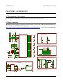
1
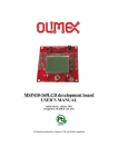
MSP430-P2618 development board
USER’S MANUAL
Initial release, January 2013
Designed by OLIMEX Ltd, 2013
All boards produced by Olimex LTD are ROHS compliant
OLIMEX© 2012
MSP430-P2618 user's manual
Disclaimer
© 2013 Olimex Ltd. Olimex®, logo and combinations thereof, are registered trademarks of Olimex Ltd.
Other product names may be trademarks of others and the rights belong to their respective owners.
The information in this document is provided in connection with Olimex products. No license, express
or implied or otherwise, to any intellectual property right is granted by this document or in connection
with the sale of Olimex products.
The Hardware project is released under closed source terms. You will have to provide a link to the original
creator of the project http://www.olimex.com on any documentation or website. You may also modify the
files, but you must then release them as well under the same terms. Credit can be attributed through a link to
the creator website: http://www.olimex.com
The software is released under GPL.
It is possible that the pictures in this manual differ from the latest revision of the board.
The product described in this document is subject to continuous development and improvements. All
particulars of the product and its use contained in this document are given by OLIMEX in good faith.
However all warranties implied or expressed including but not limited to implied warranties of
merchantability or fitness for purpose are excluded. This document is intended only to assist the reader in the
use of the product. OLIMEX Ltd. shall not be liable for any loss or damage arising from the use of any
information in this document or any error or omission in such information or any incorrect use of the
product.
This evaluation board/kit is intended for use for engineering development, demonstration, or evaluation
purposes only and is not considered by OLIMEX to be a finished end-product fit for general consumer use.
Persons handling the product must have electronics training and observe good engineering practice
standards. As such, the goods being provided are not intended to be complete in terms of required design-,
marketing-, and/or manufacturing-related protective considerations, including product safety and
environmental measures typically found in end products that incorporate such semiconductor components or
circuit boards.
Olimex currently deals with a variety of customers for products, and therefore our arrangement with the user
is not exclusive. Olimex assumes no liability for applications assistance, customer product design, software
performance, or infringement of patents or services described herein.
THERE IS NO WARRANTY FOR THE DESIGN MATERIALS AND THE
COMPONENTS USED TO CREATE MS430-P2618. THEY ARE CONSIDERED
SUITABLE ONLY FOR MSP430-P2618.
Page 2 of 23
OLIMEX© 2012
MSP430-P2618 user's manual
Table of Contents
Disclaimer.....................................................................................................................2
CHAPTER 1 | OVERVIEW....................................................................................... 5
1.1 Introduction to the chapter.....................................................................................................5
1.2 Features.....................................................................................................................................5
1.3 Organization.............................................................................................................................5
CHAPTER 2 | SETTING UP THE MSP430-P2618 BOARD..................................7
2.1 Introduction to the chapter.....................................................................................................7
2.2 Electrostatic warning...............................................................................................................7
2.3 Requirements........................................................................................................................... 7
2.4 Powering the board..................................................................................................................8
2.5 Prebuilt software......................................................................................................................8
CHAPTER 3 | MSP430-P2618 BOARD DESCRIPTION....................................... 9
3.1 Introduction to the chapter.....................................................................................................9
3.2 Layout (top view).....................................................................................................................9
CHAPTER 4 | THE MSP430F2618 MICROCONTROLLER..............................10
4.1 Introduction to the chapter...................................................................................................10
4.2 The microcontroller...............................................................................................................10
CHAPTER 5 | CONTROL CIRCUITY...................................................................12
5.1 Introduction to the chapter...................................................................................................12
5.2 Reset........................................................................................................................................12
5.3 Clocks......................................................................................................................................12
CHAPTER 6 | HARDWARE....................................................................................13
6.1 Introduction to the chapter...................................................................................................13
6.2 JTAG connector.....................................................................................................................13
6.3 UEXT connector.................................................................................................................... 14
6.4 RS232 connector.................................................................................................................... 14
6.5 PWR jack................................................................................................................................15
6.6 Column pads (near the proto area)......................................................................................15
6.7 Battery connector...................................................................................................................16
6.8 Jumper description................................................................................................................17
6.9 Additional hardware components........................................................................................ 17
CHAPTER 7 | MEMORY AND BLOCK DIAGRAM...........................................18
7.1 Introduction to the chapter...................................................................................................18
7.2 Memory organization............................................................................................................ 19
CHAPTER 8 | SCHEMATICS.................................................................................20
Page 3 of 23
OLIMEX© 2012
MSP430-P2618 user's manual
8.1 Introduction to the chapter...................................................................................................20
8.2 Eagle schematic......................................................................................................................20
8.3 Dimensions..............................................................................................................................21
CHAPTER 9 | REVISION HISTORY.....................................................................22
9.1 Introduction to the chapter...................................................................................................22
9.2 Document revision................................................................................................................. 22
9.2 Board revision........................................................................................................................ 22
9.3 Web page of your device....................................................................................................... 23
Page 4 of 23
OLIMEX© 2012
MSP430-P2618 user's manual
CHAPTER 1 | OVERVIEW
1.1 Introduction to the chapter
Thank you for choosing the MSP430-P2618 development board from Olimex! This document
provides a user’s guide for the Olimex MSP430-P2618 development board. As an overview, this
chapter gives the scope of this document and lists the board’s features. The document’s
organization is then detailed.
The MSP430-P2618 development board enables code development of applications running on the
MSP430F2618 microcontroller, manufactured by Texas Instruments.
1.2 Features
●
●
●
●
●
●
●
●
●
●
●
●
●
●
●
●
●
MCU: MSP430F2618 with 116 KB + 256 B Flash Memory, 8 KB RAM
JTAG connector
RS232 driver + RS232 connector
User button
Power supply LED
User status LED
32 768 Hz oscillator crystal
Optional high frequency crystal (socket)
RESET button
External power supply jack for AC or DC power supply
Voltage regulator + power supply filtering capacitor
Extension headers for all uC pins
Prototype area with 0.2'' step, Vcc + GND bus
UEXT connector
Connector for lithium polymer battery
PCB: FR-4, 1.5 mm (0.062''), red soldermask
Dimensions 99.38 x 79.31 mm (3.91 x 3.12")
1.3 Organization
Each section in this document covers a separate topic, organized as follows:
–
Chapter 1 is an overview of the board usage and features
Page 5 of 23
OLIMEX© 2012
MSP430-P2618 user's manual
–
–
Chapter 2 provides a guide for quickly setting up the board
Chapter 3 contains the general board diagram and layout
–
Chapter 4 describes the component that is the heart of the board: the MSP430F2618
microcontroller
Chapter 5 is an explanation of the control circuitry associated with the microcontroller to
reset. Also shows the clocks on the board
–
–
–
Chapter 6 covers the connector pinout, peripherals and jumper description
Chapter 7 shows the processor diagram and memory map
–
–
Chapter 8 provides the schematics
Chapter 9 contains the revision history
Page 6 of 23
OLIMEX© 2012
MSP430-P2618 user's manual
CHAPTER 2 | SETTING UP THE MSP430-P2618 BOARD
2.1 Introduction to the chapter
This section helps you set up the MSP430-P2618 development board for the first time.
Please consider first the electrostatic warning to avoid damaging the board, then discover the
hardware and software required to operate the board.
The procedure to power up the board is given, and a description of the default board behavior is
detailed.
2.2 Electrostatic warning
MSP430-P2618 is shipped in a protective anti-static package. The board must not be exposed to
high electrostatic potentials. A grounding strap or similar protective device should be worn when
handling the board. Avoid touching the component pins or any other metallic element.
2.3 Requirements
In order to set up the MSP430-P2618, the following items are required:
- A source of power – the board can be powered through JTAG connector; or through the external
power jack connector.
- Debugger supporting 14 pin JTAG interface and the used microcontroller MSP430F2618.
All our MSP430 programmers are recommended for MSP430-P2618:
- Olimex MSP430-JTAG-TINY-V2 – small emulator/programmer ideal for beginners:
https://www.olimex.com/Products/MSP430/JTAG/MSP430-JTAG-TINY-V2/
- Olimex MSP430-JTAG-ISO-MK2 – our best MSP430 emulator/programmer (featuring display,
SD card and 3 modes of operation):
https://www.olimex.com/Products/MSP430/JTAG/MSP430-JTAG-ISO-MK2/
- Olimex MSP430-JTAG-RF – the first wireless MSP430 emulator/programmer:
https://www.olimex.com/Products/MSP430/JTAG/MSP430-JTAG-RF/
Also, a host-based software toolchain is required in order to program/debug the MSP430-P2618
board. There are also a number of ready IDEs available like IAR Embedded Workbench, Rowley
CrossWorks, Code Composer Studio, etc.
Page 7 of 23
OLIMEX© 2012
MSP430-P2618 user's manual
We also provide our own flash programming software which can be distributed free. You can find it
at the above mentioned debuggers' web pages.
2.4 Powering the board
There are two options for powering the board:
Either set the jumpers P_IN closed, P_OUT open so you can power from JTAG connector
OR open P_IN, close P_OUT jumper and then use the power jack connecter to provide 5V DC.
Note: In previous revisions there was an option to provide 6.5V AC, which is no longer the case.
On powering the board the PWR LED, LED1 should turn on.
2.5 Prebuilt software
On powering the board the PWR LED should turn on. The LCD should show 3 lines of text and the
ability to control the selector marker between them. On pressing the joystick over our test of choice
it should be conducted.
Page 8 of 23
OLIMEX© 2012
MSP430-P2618 user's manual
CHAPTER 3 | MSP430-P2618 BOARD DESCRIPTION
3.1 Introduction to the chapter
Here you get acquainted with the main parts of the board. Note the names used on the board differ
from the names used to describe them. For the actual names check the MSP430-P2618 board itself.
3.2 Layout (top view)
Page 9 of 23
OLIMEX© 2012
MSP430-P2618 user's manual
CHAPTER 4 | THE MSP430F2618 MICROCONTROLLER
4.1 Introduction to the chapter
In this chapter is located the information about the heart of MSP430-P2618 – its microcontroller.
The information is a modified version of the datasheet provided by its manufacturers.
4.2 The microcontroller
Features:
● Low Supply Voltage Range, 1.8 V to 3.6 V
● Ultra-Low Power Consumption:
- Active Mode: 365 µA at 1 MHz, 2.2 V
- Standby Mode: 0.5 µA
- Off Mode (RAM Retention): 0.1 µA
● Wake-Up From Standby Mode in Less Than 1µs
● 16-Bit RISC Architecture, 62.5-ns Instruction Cycle Time
● Three-Channel Internal DMA
● 12-Bit Analog-to-Digital (A/D) Converter With Internal Reference,
Sample-and-Hold, and Autoscan Feature
● Dual 12-Bit Digital-to-Analog (D/A) Converters With Synchronization
● 16-Bit Timer_A With Three Capture/Compare Registers
● 16-Bit Timer_B With Seven Capture/Compare-With-Shadow Registers
● On-Chip Comparator
● Four Universal Serial Communication Interfaces (USCIs)
- USCI_A0 and USCI_A1
- Enhanced UART Supporting Auto-Baudrate Detection
- IrDA Encoder and Decoder
- Synchronous SPI
- USCI_B0 and USCI_B1
- I2C
- Synchronous SPI
● Supply Voltage Supervisor/Monitor With Programmable Level Detection
● Brownout Detector
● Bootstrap Loader
Page 10 of 23
OLIMEX© 2012
MSP430-P2618 user's manual
● Serial Onboard Programming, No External Programming Voltage Needed
Programmable Code Protection by Security Fuse
● 116KB+256B Flash Memory, 8KB RAM
1
For comprehensive information on the microcontroller visit the Texas Instruments web page for a
datasheet.
At the moment of writing the microcontroller datasheet can be found at the following link:
http://www.ti.com/lit/ds/symlink/msp430f2618.pdf
Page 11 of 23
OLIMEX© 2012
MSP430-P2618 user's manual
CHAPTER 5 | CONTROL CIRCUITY
5.1 Introduction to the chapter
Here you can find information about reset circuit, power circuit and quartz crystal locations.
5.2 Reset
MSP430-P2618 reset circuit features a capacitor C36(47n) and processor pin 58(RST/NMI). You
could also reset the MCU with an active low level at the JTAG pin 11.
5.3 Clocks
Real time clock (RTC) 32 768Hz Q1 is connected to pins 8 and 9 of the processor.
A free socket for custom quartz crystal Q2 is connected to pins 52 and 53 of the processor.
Page 12 of 23
OLIMEX© 2012
MSP430-P2618 user's manual
CHAPTER 6 | HARDWARE
6.1 Introduction to the chapter
In this chapter are presented the connectors that can be found on the board all together with their
pinout. Proto area is shown. Jumpers functions are described. Notes and info on specific peripherals
are presented. Notes regarding the interfaces are given.
6.2 JTAG connector
The 14 pin JTAG connector provides the interface for JTAG programming/debugging. The plastic
connector is situated at the bottom of the board. The pinout can be found in the table below.
JTAG Connector
Pin #
Signal Name
Pin #
Signal Name
1
TDO
8
Not connected
2
P_IN/NC*
9
GND
3
TDI
10
Not connected
4
NC/P_OUT*
11
#RST
5
TMS
12
Not connected
6
Not connected
13
Not connected
7
TCK
14
Not connected
*Depending on the jumper P_OUT/P_IN position
Page 13 of 23
OLIMEX© 2012
MSP430-P2618 user's manual
6.3 UEXT connector
UEXT is used to connect expansion modules made by Olimex. It features SPI, UART and I2C
(when all three are available at the microcontroller)
UEXT Connector
Pin #
Signal Name
1
+3.3V
2
GND
3
UTXD1
4
URXD1
5
SCL1
6
SDA
7
SOMI1
8
SIMO1
9
UCLK1
10
STE1
6.4 RS232 connector
RS232
Pin #
Signal Name
1
NC
2
T2OUT
3
R1IN
4
NC
5
GND
6
NC
7
NC
8
NC
Page 14 of 23
OLIMEX© 2012
9
MSP430-P2618 user's manual
NC
T2OUT - Output Transmit Data. This is the transmit data line for the RS232 interface.
R1IN - Input Receive Data. This is the receive data line for the RS232 interface.
6.5 PWR jack
Note that the board should be powered by only 5V DC.
PWR jack
Pin #
Signal Name
1
PWR
11
GND
6.6 Column pads (near the proto area)
Important: the top row of the proto area is 3.3V; the bottom row is GND. Be careful with
shortcircuit!
The pads have their names printed on the board.
Pin #
Signal Name
Pin #
Signal Name
1
VCC
2
GND
3
P6.6
4
P6.7
5
P6.4
6
P6.5
7
P6.2
8
P6.3
9
P6.0
10
P6.1
11
VCC
12
GND
13
P5.6
14
P5.7
15
P5.4
16
P5.5
17
P5.2
18
P5.3
Page 15 of 23
OLIMEX© 2012
MSP430-P2618 user's manual
19
P5.0
20
P5.1
21
VCC
22
GND
23
P4.6
24
P4.7
25
P4.4
26
P4.5
27
P4.2
28
P4.3
29
P4.0
30
P4.1
31
VCC
32
GND
33
P3.6
34
P3.7
35
P3.4/TXD0
36
P3.5/RXD0
37
P3.2
38
P3.3
39
P3.0
40
P3.1
41
VCC
42
GND
43
P2.6
44
P2.7
45
P2.4
46
P2.5
47
P2.2
48
P2.3
49
P2.0
50
P2.1
51
VCC
52
GND
53
P1.6
54
P1.7
55
P1.4
56
P1.5
57
P1.2
58
P1.3
59
P1.0
60
P1.1
6.7 Battery connector
When using the battery connector keep in mind that it is an energy solution that wouldn't be able to
power the board and all the peripherals. The voltage of a 3.7V LIPO battery would be enough to
power the processor and the memory but won't be enough to power external touchscreen LCD.
Pin #
Signal Name
1
VIN
2
GND
Page 16 of 23
OLIMEX© 2012
MSP430-P2618 user's manual
6.8 Jumper description
P_OUT/P_IN - This jumper controls power on pins 2 and 4 of the JTAG connector. When in
P_OUT is closed 3.3V can be measured at pin 4.
Check the schematic for more info.
Default position is P_OUT – closed, P_IN - open.
6.9 Additional hardware components
The components below are mounted on MSP430-P2618 but are not discussed above. They are listed
here for completeness:
User button with name BUT connected to MSP430F2618 pin 60 (P6.1/A1).
Reset button with name RST connected to MSP430F2618 pin 58 (RST/NMI).
Power LED with name PWR – lights when the board is power supplied.
Status red LED with name LED connected to MSP430F2618 pin 59 (P6.0/A0).
Page 17 of 23
OLIMEX© 2012
MSP430-P2618 user's manual
CHAPTER 7 | MEMORY AND BLOCK DIAGRAM
7.1 Introduction to the chapter
At the right side of the page is
located the block diagram of the
processor and on the next page
you can find a memory map for
this family of processors. It is
strongly recommended to refer to
the original datasheet released by
Texas Instruments for ones of
higher quality.
Page 18 of 23
OLIMEX© 2012
MSP430-P2618 user's manual
7.2 Memory organization
Page 19 of 23
OLIMEX© 2012
MSP430-P2618 user's manual
CHAPTER 8 | SCHEMATICS
8.1 Introduction to the chapter
In this chapter is located the schematic describing logically MSP430-P2618.
8.2 Eagle schematic
3.3V
U1
C3
C2
10uF/6.3V
100n
10uF/6.3V
0R
C7
NA
P2.0/ACLK
P2.1/TACLK
P2.2/CAOUT
P2.3/CA0
P2.4/CA1
P2.5/ROSC
P2.6/ADCLK
P2.7/TA0
P3.0/STE0
P3.1/SIMO0
P3.2/SOMI0
P3.3/ULCK0
P3.4/UTXD0
P3.5/URXD0
P3.6/UTXD1
P3.7/URXD1
Q2
NA
Q1
32768Hz
C4
C5
8
9
C8
20pF
C9
20pF
RST
JTAG
1
2
3.3V
HN1x2
1
2
P_OUT
HN1x2
14
12
10
8
6
4
2
XT2IN
XT2OUT
P4.0/TB0
P4.1/TB1
P4.2/TB2
P4.3/TB3
P4.4/TB4
P4.5/TB5
P4.6/TB6
P4.7/TBCLK
TCK
TDI
TDO/TDI
TMS
P5.0/STE1
P5.1/SIMO1
P5.2/SOMI1
P5.3/UCLK1
P5.4/MCLK
P5.5/SMCLK
P5.6/ACLK
P5.7/TH
10pF
10pF
13
11
9
7
5
3
1
Q3
53
52
57
55
54
56
XIN
XOUT/TCLK
P_IN
V+
3.3V
R6
V+
0R
R10
3.3V
0R
P6.0/A0
P6.1/A1
P6.2/A2
P6.3/A3
P6.4/A4
P6.5/A5
P6.6/A6
P6.7/A7
C14
100n
64
62
C13
1
63
100n
AVCC
AVSS
DVCC
DVSS
P2.0
P2.1
P2.2
P2.3
P2.4
P2.5
P2.6
P2.7
28
29
30
31
32
33
34
35
PWR_RS
SDA_1XX/SDA_2XX
SCL_2XX
SCL_1XX
TXD0
RXD0
UTXD1
URXD1
36
37
38
39
40
41
42
43
P3.0
P3.1
P3.2
P3.3
P3.4
P3.5
P3.6
P3.7
P4.0
P4.1
P4.2
P4.3
P4.4
P4.5
P4.6
P4.7
44
45
46
47
48
49
50
51
STE1
SIMO1
SOMI1
UCLK1
59
60
61
2
3
4
5
6
LED
BUT
P5.0
P5.1
P5.2
P5.3
P5.4
P5.5
P5.6
P5.7
P6.0
P6.1
P6.2
P6.3
P6.4
P6.5
P6.6
P6.7
3.3V
20
21
22
23
24
25
26
27
LED & BUT
3.3V_1
GND_1
3.3V
3.3V
R2
100k
LED
LED_GREEN_0603
R4
B1
3.3V_2
GND_2
R12
2k
B UT
330R
BUT
LED
3.3V_3
GND_3
UEXT
3V3
3.3V_4
GND_4
SCL_1XX
3V3
R7
100k
3.3V_5
GND_5
SCL_2XX
3V3
R8
100k
3V3
R9
100k
UTXD1
URXD1
SCL
SDA_1XX/SDA_2XX
1
VREF+
R13
VEREF+
VREF+
VREF-
P1.0
P1.1
P1.2
P1.3
P1.4
P1.5
P1.6
P1.7
2
SOMI1
3
10
7
11
12
13
14
15
16
17
18
19
3.3V
NA
R11
P1.0/TACLK
P1.1/TA0
P1.2/TA1
P1.3/TA2
P1.4/SMCLK
P1.5/TA0
P1.6/TA1
P1.7/TA2
NA(1nF)
3.3V
0R
R3
C18
RST/NMI
3.3V
58
3.3V
RST
SCL_2XX/SCL_1XX
R14
47k
RST
R1
3.3V
V+
V+
MSP430-P2618 schematic is visible for reference here. You can also find it with higher quality on
the web page for MSP430-P2618 at our site:
https://www.olimex.com/Products/MSP430/Starter/MSP430-P2618/. It is located in HARDWARE
section.
SIMO1
UCLK1
STE1
UEXT-1
UEXT-2
UEXT-3
UEXT-4
UEXT-5
UEXT-6
UEXT-7
UEXT-8
UEXT-9
UEXT-10
BH10S
BH10S
BH10S
BH10S
BH10S
BH10S
BH10S
BH10S
BH10S
BH10S
3.3V_6
GND_6
MSP430F2618
POWER_SUPPLY
PWR_J
VR1(3.3V)
M CP1700T -3302E/MB
TXD0
4
C2+
5
C2-
11
10
RXD0 12
9
T1IN
T2IN
R1OUT
R2OUT
V-
6
C1
100n
C6
100n
R5
22R
U2PWR
15GND
RS232
T1OUT
T2OUT
R1IN
R2IN
14
7
13
8
1
2
3
4
5
16
VCC
3
C12
100n
V+
C1-
2
2
1
3
C1+
6
7
8
9
C10
100n
PWR_RS
3.3V/PWR_RS
1
GND
3.3V
ST3232CD
Page 20 of 23
R15
2k
+
1
2
3.7V-LI_B AT
DW02R
-
10uF/6.3V
PWR
U2
C11
100n
1
MSP430-P2618_rev_D
OLIMEX LTD, BULGARIA
https://www.olimex.com
3.3V
VIN
VOUT
3
GND
C15
C17
2
1
RS232
BAT54C
D1
CLOSE
5VDC
PWR_LED_E
2
100n
GND_7
C16
10uF/6.3V
OLIMEX© 2012
MSP430-P2618 user's manual
8.3 Dimensions
Note that the dimensions of the board are in mils.
Page 21 of 23
OLIMEX© 2012
MSP430-P2618 user's manual
CHAPTER 9 | REVISION HISTORY
9.1 Introduction to the chapter
In this chapter you will find the current and the previous version of the document you are reading.
Also the web-page for your device is listed. Be sure to check it after a purchase for the latest
available updates and examples.
9.2 Document revision
Revision
Changes
Modified
Pages
C
Initial release
All
D
Recreated document
All
9.2 Board revision
Revision
D
Changes
UEXT added
Lithium battery connector added
Lowered PROTO area size
Removed AC rectifier
LM1117 changed with a lower power 3.3V regulator
Optimized the schematic for lower power
Page 22 of 23
OLIMEX© 2012
MSP430-P2618 user's manual
9.3 Web page of your device
The web page you can visit for more info on your device is
https://www.olimex.com/Products/MSP430/Proto/MSP430-P2618/. There you can find more info
and some examples.
ORDER CODES:
MSP430-P2618 - completely assembled and tested
MSP430-JTAG-TINY-V2 – mini emulator/programmer USB<->JTAG 14p
MSP430-JTAG-ISO-MK2 – our best MSP430 emulator/debugger with extra features
MSP430-JTAG-RF – wireless emulator/programmer USB<->JTAG 14p
How to order?
You can order directly from our web shop or from any of our distributors.
Check our webpage https://www.olimex.com/ for more info. For the full list of distributors
visit https://www.olimex.com/Distributors/.
Page 23 of 23