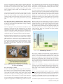
1
the journal Issue 76 May 2008 ISSN 1748-9253 EMI Simulation Software Feature See Page 25 1 Multimedia Equipment (MME) Standards See Page 17 2 News and Information 5 10 14 16 17 25 27 the What's In This Issue 33 Choosing Software for EMC Simulation By Paul Duxbury, CST GmbH 36 Proper Signal Integrity Design Reduces EMI By Aki Nakatani, Ansoft and Hiroshi Higashitani, Panasonic Electronic Devices 39 EMC Simulation Products 42 Product Gallery 43 Part 6 - ESD, electromechanical devices, power factor correction, voltage fluctuations, supply dips and dropouts. (3rd part) By Keith Armstrong, Cherry Clough Consultants 54 Advertisers Index Product Gallery EMCUK Academy Training John Woodgate’s Column The Multimedia Equipment (MME) Standards By John Davies, Blackwood Compliance Labs. Special Feature - EMI Simulation Software Software Simulation Tools and Proper Validation for EMC Control in the Real-World By Bruce Archambeault, IBM journal www.theemcjournal.com www.emcia.org www.emcuk.co.uk www.emcuk.co.uk/academy Every effort has been made to ensure that the information given in this Journal is accurate, but no legal responsibility is accepted for any errors, omissions or misleading statements in that information caused by negligence or otherwise, and no responsibility is accepted in regard to the standing of any firms, companies or individuals mentioned or for any advice or information given by them. 3 The EMC Journal May 2008 The EMC Journal May 2008 4 The EMC Journal Free to readers worldwide May 2008 - Issue No. 76 Published every other month First Issue March 1995 Editorial & Publishing Director: Alan E Hutley [email protected] New President for EMC Industry Association At the recent AGM held in London the EMCIA appointed Keith Armstrong of Cherry Clough Consultants as their New President. Keith will hold this position for a term of two years in line with the Association’s constitution. The appointment follows the standing down of Vic Clements at the end his of his term. Vic will now become Vice President and continue many important functions for the EMCIA. Technical Consultant: Dave Fynn [email protected] Keith is well known internationally through publication of his many articles, demonstrations and training courses on EMC. Keith is a member of the IET and IEEE and chairs the IET Working Group on EMC & Functional Safety. Advertisement Sales Director: Lynne S Rowland [email protected] Production & Circulation Director: Pam A Hutley [email protected] The EMCIA was formed on 20th March 2002 for the benefit of companies involved in Supplying, Designing, Testing and Manufacturing EMC products. Networking lunches are held 3 times a year. Nutwood UK Ltd Eddystone Court, De Lank Lane, St. Breward, Bodmin, Cornwall PL30 4NQ Tel: +44 (0)1208 851530 Fax: +44 (0)1208 850871 Web: www.theemcjournal.com © Nutwood UK Limited May 2008 More information on EMCIA and its members, including Keith’s full biography can be found on the EMCIA website www.emcia.org. Front Cover Hero circle, CST GmbH, pages 24/33/40 Circle top, TBAECP, page 10 Circle middle, TTi, page 42 Circle bottom, Chomerics, page 10 Secretariat for EMCIA SELEX On the Move Hart Materials Ltd SELEX Communications has begun the relocation of its operations currently situated at Chelmsford and Great Baddow to Finmeccanica’s site in Basildon, where it will be situated alongside - but separate from the facilities of its sister company SELEX GALILEO (formerly SELEX Sensors and Airborne Systems. Tel: +44 (0)1268 823400 www.selex-comms.co.uk Hart Coating Technology has been active as a specialised materials supply company since 1984. However it ceased to trade from 31st March 2008 when activities were transferred to a new company Hart Materials Ltd, commencing operations immediately on 1st April 2008. The Trade Association for the EMC Industry. Web: www.emcia.org The EMC Journal Supports EMCUK Academy EMC Information Centre Check out our website www.theemcjournal.com www.emcuk.co.uk/academy 5 The continued successful expansion of Hart Coating Technology during the last few years has made this change necessary in order to facilitate the continuing growth of the business and enable continuity of activity to be maintained in the future. No radical changes are planned at the moment, Dr. Tony Hart will be continuing his present activities but in the new role of Chairman and Managing Director and Nikki Davies, remains as Administration Manager. [email protected] www.hartmaterials.com IEEE EMC Symposium 18-22 August 2008 Detroit, USA www.emc2008.org The EMC Journal May 2008 News and Information AR RF/Microwave Instrumentation announces appointment of Bud Osthaus as Microwave Design Specialist New EMC Facilities Manager for TRaC Global microelectronics experience to the company. Mr. Osthaus began his career as a designer with Microcom Corp. and later worked in process engineering for a variety of technology companies. Prior to joining AR, he was with Merrimac Industries, where he established a full-service microelectronic prototype facility. AR has expanded its staff of Microwave Design Specialists with the addition of Bud Osthaus, who brings 30 years of In AR’s quest to create state of the art, highly reliable RF and Millimeter Wave microelectronic products, Bud will be developing assembly processes and equipment. His experience in military and high volume commercial electronics manufacturing will play a key role in keeping AR at the fore-front of technology in a global market. www.ar-worldwide.com Chomerics Europe appoints new Sales Manager for Germany, Austria and Switzerland Chomerics Europe has appointed Tiberius Recean as Territory Sales Manager for Germany, Austria and Switzerland. From his base close to Munich, Tiberius will provide customers with both technical and commercial support for Chomerics’ industryleading range of EMI shielding and thermal management products. Key market sectors include automotive and telecoms, plus military and aerospace. Tiberius has a strong background and experience in communications engineering and electrical / electronic engineering. Prior to joining Chomerics Europe, he spent eight years working in a sales engineering role for a cable manufacturer, and before that, was employed as a Key Account Manager for a Carlos Perkins has joined the TRaC Global Group to run its EMC Projects test laboratory in Ringwood, Hampshire. Carlos, 48, brings over 20 years' experience in EMC and TEMPEST approvals to TRaC, having worked for leading organisations around the world, including MIRA, Rohde and Schwarz, Nokia, Marconi, QinetiQ and, most recently, EADS Casa. Carlos' appointment is part of the ongoing investment in people and facilities at TRaC Global, which comprises world class specialist test laboratories TRL Compliance, KTL, Cape and EMC Projects. He will be responsible for the day to day management of facilities and operations at the group's South of England laboratory, near Ringwood. Having been working at the cutting edge of technological developments for military and aerospace applications, Carlos has the skills to manage the qualification process quickly and efficiently. leading power supply manufacturer. www.chomerics.com EMC Yearbook 2008 Have you got your copy? If not, email [email protected] with your full details and we’ll pop one in the post. 6 Commenting on his new position, Carlos says: “I am joining TRaC Global at an exciting time in its development and see this is a tremendous opportunity to use my experience and knowledge to help move the group forward.” www.tracglobal.com 7 News and Information New Lower Cost Testing Service TÜV Product Service is launching a new lower cost service to complement its existing broad scope of EMC testing services. The new test service will appeal particularly to companies wishing to test their products’ EMC compliance during design and development. In order to offer this service, TÜV Product Service has invested in a large G-TEM Cell for EMC radiated emissions and immunity testing, which will form the basis for the new service at its test facility in Fareham, Hampshire and will complement its existing 11 EMC chambers. The G-TEM Cell offers a lower cost alternative to conventional screened rooms for radiated emissions and immunity precompliance or confidence testing. However, full compliance radiated immunity testing to EN 61000-4-20 (as an alternative to EN 61000-4-3) and radiated emissions testing can also be performed in the G-TEM Cell. Measurements made with a G-TEM Cell are accepted for final compliance demonstration by the FCC for Part 15 & 18 radiated emissions testing. This new service will be highly beneficial to companies who wish to conduct EMC development and investigatory work on their products as experience shows that many products fall short of mandatory or contractual EMC performance requirements. Typically, manufacturers’ main design focus is on functionality, aesthetics and cost, but identifying and resolving EMC issues at the earliest possible stage of development can save considerable time and money later on in the development process. TÜV Product Service’s ‘G-TEM Experience’ allows manufacturers affordable access to EMC testing whether it be for just a quick check or to investigate and modify designs, thereby helping to ensure that products are on track to pass formal EMC compliance testing at the first attempt. To find out more about G-TEM Cell testing or our other EMC, Radio, Product Safety, Environmental, Climatic, Shock & Vibration testing capabilities, please contact TÜV Product Service on +44 (0)1489 558100 or email [email protected]. www.tuvps.co.uk Syfer caps it all with Queen’s Award Leading European capacitor manufacturer, Syfer Technology, has won a 2008 Queen’s Award for Enterprise. This highly prestigious award for Innovation is for the development of Syfer’s FlexiCapTM capacitor termination technology. Syfer joins the ranks of other leading UK innovators recognised this year for making a significant contribution to British industry, including Du Pont, Land Rover, Picsel Technologies and Symbian. Managing Director of Syfer Technology, Howard Ingleson commented: “Many of the products made with our components are used in safety-critical environments, so precision and quality are paramount,” In recent years, Syfer has pioneered several cutting-edge production techniques and component designs to meet customer demands. “We’re delighted and proud that our efforts have been officially acknowledged with this Queen’s Award,” he added. Syfer Technology based near Norwich, UK, employs 275 people involved in research and CEM 2008 A great success The Computational in Electromagnetics Conference held at the Old Ship hotel Brighton in early April was extremely well attended with around a 100 people across the three days. Very Professionally organised by the IET Electromagnetics and EMC PN. The conference was also professionally Chaired by Dr Liz Davenport BAE Systems Technology Centre supported by the Chair of the Electromagnetics TPN Professor Jan Sykulski. More information on papers presented at the conference can be obtained by emailing Sarah Halfpenny, TPN Manager: [email protected] Information on all the IET PN's and how to join can be found at web site: http:// www2.theiet.org/oncomms/sector/ We thank Professor Jan Sykulski, University of Southampton for providing the photo. The EMC Journal May 2008 8 Howard Ingleson development, design, manufacturing, technical support, sales and marketing. Syfer’s products are widely used in the industrial, telecoms, avionics, automotive and aerospace sectors. www.syfer.com ANSYS, Inc. signs definitive agreement to acquire Ansoft Corporation ANSYS, Inc. (NASDAQ: ANSS), a global innovator of simulation software and technologies designed to optimize product development processes, and Ansoft Corporation (NASDAQ: ANST), a global provider of Electronic Design Automation (EDA) software, announced today that they signed a definitive agreement whereby ANSYS will acquire Ansoft for a purchase price of approximately $832 million in a mix of cash and ANSYS common stock. The strategic, complementary business combination of ANSYS and Ansoft will create the leading provider of ‘best-in-class’ simulation capabilities, with combined trailing 12-month revenues of $485 million. When completed, ANSYS currently anticipates that the transaction will be modestly accretive to non-GAAP earnings per share in its first full year of combined operations. “The combination of Ansoft’s extensive portfolio of electromagnetics, circuit and systems simulation solutions with ANSYS’ existing simulation capabilities creates a ‘best of breed’ company that will continue to lead the evolution and innovation of engineering simulation by enabling customers to improve their product development processes, eliminate physical prototypes, reduce timeto-market for new products and improve product innovation and performance,” said Nicholas Csendes, President and Chief Executive Officer of Ansoft. www.ansys.com www.ansoft.com 9 Product gallery Comprehensive Beryllium Copper product line for EMI/RFI shielding from TBA ECP EMI shielding specialist, TBA Electro Conductive Products (ECP) now offers one of the UK’s most comprehensive ranges of Beryllium Copper EMI/RFI shielding strips available from a single source. The company’s portfolio of BeCu EMI/RFI shielding products is one of the largest standard ranges of fingerstock profiles available in the UK and, in many instances, the company can despatch from stock. In the unlikely event of a profile being out of stock, most profiles can be despatched within two weeks. Profiles are available in full lengths (usually 406mm) or can be supplied cut down to customer requirements. Fingerstock BeCu shielding strips are available in an extensive range of mounting styles including clipon, stick-on, snap-on, special mounting products, low profile and hook-on gaskets and connector gaskets. A wide range of plating options is available including clean and bright, gold, silver, bright tin, bright nickel, zinc/clear chromate and electroless nickel among fabric types. When used in sliding applications, BeCu gaskets are selfcleaning. Engineers’ Design Packs, featuring small samples of BeCu gaskets presented in an A4 folder, are available to help designers choose the correct profile for the job. The company can also cross refer competitor part numbers so if a customer has been let down by a supplier or their original supplier stops providing the part, TBA ECP is usually able to offer a direct or very near equivalent replacement. Complementing its range of beryllium copper shielding strips, TBA ECP also supplies stainless steel versions of its low-profile and pressure sensitive mounting gaskets. These extend the choice of materials available to design engineers and provide hardwearing and long-lasting EMI/RFI shielding in a wide range of applications. Tel: +44 (0)1706 647718 [email protected] www.tbaecp.co.uk others. These plating options ensure compatibility with most metals, avoiding any potential problems of galvanic corrosion. Beryllium copper shielding strips offer excellent spring qualities and long life. Other important characteristics include low closing forces and high attenuation exceeding 100dB for many styles. The pure metal BeCu shielding strips deliver superior attenuation compared to fabric gaskets. Metal gaskets also offer greater longevity as they are harder wearing than Chomerics introduces electrically conductive silver epoxy coatings for EMI shielding Chomerics Europe has introduced two new electrically conductive coatings to provide EMI shielding of electronic equipment enclosures. CHO-SHIELD 576 and 579 provide shielding levels up to 80dB in the 30MHz to 1GHz range. Both may be applied by either conventional spray equipment or a brush. CHO-SHIELD 576 is a highly conductive two-component silverfilled epoxy coating. It provides excellent EMI and environmental protection when applied to glass, plastic or epoxy substrates and it may be copper or tin plated after than its predecessor. Both new CHO-SHIELD materials are touch-dry in less than one hour at room temperature. However, the best final electrical properties are achieved by curing the material at elevated temperatures. CHO-SHIELD 579 is available in 454g tins, whilst CHO-SHIELD 576 may be supplied in either 454g or 2.270Kg tins. Tel: +44 (0)1628 404000 [email protected] www.chomerics.com application. CHO-SHIELD 579 is also a twocomponent, silver-filled coating. The material has been specifically developed to have a low level of volatile organic compounds (VOCs) and achieves a VOC rating of just 357 grams/litre - 40% lower Member AR introduces two new Antennas for RFI/EMI Field Testing AR RF/Microwave Instrumentation has introduced two compact, lightweight antennas for RFI/EMI field testing. The new models – AT4418 and AT4403 – are designed to supply constant high intensity field necessary for testing within and beyond the confines of a shielded room. They can also be used to perform emissions measurements and to generate the response required for many common tests in their frequency ranges. The EMC Journal May 2008 Model AT4418 covers the 1 – 18 GHz frequency range and can handle 300 watt CW input power. It provides a minimum gain of 7dB over isotropic. Model AT4403 spans the 200 MHz – 2 GHz range and is intended for 1000 watts CW input power. It provides a minimum gain of 5dB isotropic. Both antennas are extremely mobile, they mount easily on a tripod, and are built to stand up to the demands of outdoor use. Tel: +1 215 723 8181 www.ar-worldwide.com 10 New LaserPro™ Probe measures from 10kHz to 1GHz ETS-Lindgren has announced a new LaserPro™ Field Probe for Efield measurements between 10 kHz and 1 GHz. Features include auto-ranging, a dynamic range of 2.0 – 800 V/m, and a small physical profile for minimal field perturbation with improved isotropy. The Model HI-6122 laser powered probe joins the broadest full line of laser probes in the industry. ETS-Lindgren’s newest broadband probe is available in two versions for user convenience; laserpowered and rechargeable battery powered. Model HI-6122 is the laser-powered probe and Model HI6022 is the battery powered probe supplied with rechargeable NiMH batteries. Users of the original HI4422 and corresponding FP series probes can upgrade performance by substituting either of these two new probes and will appreciate continued compatibility with ETSLindgren field monitor packages and direct connect PC packages, including the popular TILE!™ immunity software. A2LA calibration and a three-year warranty are provided with either probe. “These new units are well suited for testing to the lower frequency test requirements of MIL-STD-461E, DO160E and the EN/SAE automotive immunity requirements. They also meet the AEMCLPR standard as related to isotropy performance,” said Dave Seabury, Senior Product Manager EME Measurement Devices for ETSLindgren. He continued, “As with all ETS-Lindgren 6000 series field probes, they offer unparalleled flexibility for system and application configuration.” Tel: +44 (0)1438 730700 [email protected] www.ets-lindgren.com Member More Products page 42 EMCTLA Special Workshop The Fast Fourier Transfer (FFT) Time Domain Method A Sea Change in RF Emissions Tests? There has been interest for some years in making EMC emissions measurements using a time domain Fast Fourier Transform (FFT) method rather than the conventional frequency domain sweep. The advantages claimed for this are principally that it allows a dramatic reduction in overall measurement time without compromising probability of intercept of transient signals, and also that it opens up new possibilities for investigative analysis of the emissions spectrum; it has the potential to be the most radical change in emissions test methods for decades. Commercial receivers are now available which include some capability of time domain analysis. This workshop will present an up-to-date review of the hardware and software as well as a critical discussion of the advantages and pitfalls of this new method. As well as presentations by the test equipment manufacturers, laboratories with experience of using the method will be offering their views of particular issues, and there will be an opportunity for a panel discussion at the end of the workshop. Test Equipment Presentions By: Venue and Date: ``Henley-in-Arden Country Club, near Birmingham, 26th June 2008 Fee: £50.00 plus VAT. Includes Lunch. 09.30 to 16.00 To register please contact Dave Imeson on 01794 323382 or Email: [email protected] Supported By: the ...News...Desk... AGM At the AGM meeting held on 9th April at the EEF, Tothill Street, London, a new President was elected, see page 5, and the Executive Committee was confirmed - Keith Armstrong, Cherry Clough Consultants, Alan E Hutley, Nutwood UK Ltd, Vic Clements, Oakmead Consulting, Paul Duxbury, CST GmbH, John Terry, HITEK Electronic Materials Ltd & Chris Marshman, York EMC Services Ltd. New Member We have a new member dB Technology based in Cambridge. They offer EMC Testing & Consultancy. www.dbtechnology.co.uk Alan Warner gets involved Alan Warner, as published in The EMC Journal, issue 74, page 8, is now becoming involved in the administration of the EMCIA. One of Alan’s projects will be to recruit new members to the EMCIA. If you are interested in joining why not join us as a guest for lunch at our next meeting. Please contact Alan for details, email: [email protected]. Exhibitions See EMCIA at EMCUK 2008, The Racecourse, Newbury, 14-15 October 2008. www.emcuk.co.uk 11 journal “EMCUK has firmly established itself as the place where the EMC Industry Networks. Far more than just an Exhibition & Conference, it is truly a Visitor, Exhibitor Experience. Very definitely not to be missed.” The Racecourse, Newbury 14/15th October 2008 Now in its Fifth Year Keep Up-to-date Register on the Website Supported By: the journal Organised by: Nutwood UK Ltd Eddystone Court, De Lank Lane, St Breward, Bodmin, Cornwall PL30 4NQ Tel: +44 (0)1208 851530 Fax: +44 (0)1208 850871 Email: [email protected] Web: www.emcuk.co.uk www.emcuk.co.uk 12 Recruitment Technical Sales Manager EMC Simulation Software Part of a global technology group with 10,000 employees and turnover in excess of $2 billion, our Client is a market leader having developed the most advanced EMC simulation software in the world, with virtual prototyping tools that enable customers to speed up their design process, achieve lowest cost, optimum performance and easier manufacturability. Reporting to the Sales Director, this post is UK based but with the opportunity to gain international experience. A background and qualification in Electrical Engineering is required, with the capability to discuss customer applications in technical depth and to demonstrate how the technology can provide the most effective solution. The post will ideally suit someone already in sales, however candidates with the right aptitude and a relevant engineering and applications background will also be considered. This is a unique career opportunity to join a dynamic, rapidly expanding organization. The remuneration package is widely negotiable and will not be a restrictive factor for the right person. Please email your CV in confidence to Peter Bucknell at [email protected] or call him on 01454 329976 13 Training Course Electronic Fundamentals for Good EMC Full Day Course including Lunch Programme: Presented By Keith Armstrong & Tim Williams EMC in circuit design & in the selection of active components Filtering and Cabling Filter configuration Components: capacitors and ferrites I/O and mains filtering Mode of propagation Unscreened cables: using twisted pair Screened cables - screen operation - transfer impedance - the effect of the connector Transducer and communications interfaces Digital design for EMC Analogue (not RF) design for EMC Switch-mode design for EMC Communication design for EMC Optoisolator design for EMC Checking device EMC characteristics Some useful references EMC Techniques for PCB layout Saving time and money Segregation Interface analysis, filtering, and suppression 0V and power planes Power supply decoupling Transmission line techniques Layer stacking Some useful references Shielding Theory Effect of apertures and seams Conductive gaskets Conductive coatings Using the shield as ground Cable layout and large enclosures Fee: £135 plus VAT including lunch, full copy of proceedings and attendance certificate. Why pay more. Supported By: the journal Venues: 24th September Manchester Region 25th September Edinburgh 14-15th October Newbury, in conjunction with If you are interested in attending one of these courses please register on the EMCUK Academy website www.emcuk.co.uk/academy or email [email protected] The EMC Journal May 2008 14 EMCUK 2008 Conference The Racecourse, Newbury 14-15th October 2008 Module 4 Rail Safety & Assurance Chaired by Ken Webb, TÜV Product Service Ltd Transfer function model for rolling stock interference coupled to telecoms cables Maya Petkova, Principle EMC Engineer & Peter Brown, EMC Engineer Network Rail Spacing requirements between LV power and communication cables based on induced voltage calculations Adam Bullivant, EMC Consultant ERA Technology Completing the Race - Class 395 EMC Safety Hurdles for 2012. Phil Beirne, Principal Consultant Lloyd’s Rail Power Quality and EMC Stuart Charles, EMC Engineer & Andrew Lallies, Systems Engineer Metronet Measurement investigations into Electromagnetic noise coupled from a high frequency ballasted lighting system to a co-located safety related communications system in an operational urban metro environment Les McCormack, Senior Consultant Engineer Atkins Rail Traction Compatibility with EE&CS Infrastructure Adrian Hines, Director (EMC Consultant) Rail Technology Consultants Ltd Independent Safety Assessments Speaker TBA Defence and Aerospace Chaired by Prof. Nigel Carter & Ian MacDiarmid, BAE Systems An Alternative Approach to Transient Testing Speaker TBA QinetiQ Gap Analysis on Military Standards Peter Dorey TÜV Product Service Ltd Defence Standard 59-411 System Assessment as applied to Vehicle Armament Systems Speaker TBA QinetiQ Cenelec Guide to Military Equipment Dave Imeson Compliance Europe Fee: £135 plus VAT including lunch and full copy of proceedings. Why pay more. Full Conference programme to be published end of June. Keep up-to-date register on our website www.emcuk.co.uk We reserve the right to make changes as required. 15 The EMC Journal May 2008 John Woodgate’s Column IEC (and undoubtedly EN in due course) 62368 (LCL; a telecoms term related to the balance of the circuit) of 24 dB if you consider only the twin-with-earth cables in a house, and 6 dB if you take into account two-way switch wiring and other cases where line and neutral wires are, or may be, separated. Then the question arises of how effective are the cables as antennas, and the answer is that the most effective antennas are precisely those unbalanced cables that create the highest conversion efficiency. Well, a CDV (first stage voting document) was circulated. I hope it didn’t come as a surprise to the committee management that it wasn’t accepted, in spite of a number of very surprising positive votes. The national committee comments have been circulated as a 282-page document, and the committee management expects to issue a new first-stage voting draft in July. That’s July this year! The voting period will be just THREE months, so national committees will have to work hard on the new document. It has been agreed that adaptive notching techniques will be used to protect amateur and some other services in the band, and it appears to have been accepted that ethnic groups are no longer dependent on HF broadcasting to keep in touch with their roots. The UK committee has pointed out that as a standard (at any rate, in Europe) it can’t co-exist with EN 60065 and EN 60950-1, because the standards are not consistent. As a ‘pre-standard’, designed to gain experience in its use and debug it, in IEC terms that would be a ‘Technical Specification’ (TS). However, a TS is ALSO supposed not to contradict any existing standard, so that route, too, seems to be blocked. If IEC issued it as a Report (in spite of it not meeting the IEC rules on the content of a report), CENELEC could not make it a standard. FASTER! FASTER! Protests continue to be made by technical committees about the pressure to shorten preparation times of standards. Reasons given include: • It’s really quite difficult to see how this situation can be resolved. It isn’t getting better with time, it’s getting worse. Within the general matter of a completely new safety standard which is based on a new principle (hazard-based), there is a huge controversy over flammability requirements for enclosures. This has set ‘consumer interest’ and ‘environmental protection’ groups at each others’ throats, so it can’t be all bad. (;-) The controversy can be summed up in a few words, instead of the tens of thousands being circulated: ‘Is it better to include toxic substances in plastics to reduce their flammability, or accept that some people will be killed by fires due to naked flames contacting those plastics?’. • • However, it seems likely that these protests will continue to be ignored, until some serious consequences result. It is the case that many standards are published with poor language and significant errors, that have to be expensively corrected. Surveillance of product EMC provisions in CENELEC and the Commission In my opinion, there are several ‘right’ answers, but they stand no chance of acceptance for commercial reasons: • • • The Commission employs an EMC Consultant, who works with CENELEC TC210 to watch over EMC provisions prepared by other CENELEC committees. This is, however, only an advisory role, and several committees have resisted the advice given by the consultant. The result is on-going concern on the part of the consultant and a general loss of efficiency. Effectively, the consultant has responsibility without authority, which is just bad management. stop using plastics for enclosures; use (costly) non-toxic flame-retardants; set legal requirements for candles and candle holders so that they don’t melt through plastic enclosures. You may also have noticed some italics in the above. HOW toxic? HOW many people? This, of course, generates an orthogonal set of dissenting views, ‘[not] significantly toxic’ and ‘[not] many people’, supported or not by concentration figures in parts per billion and press reports of fatal fires. Naturally, there are parts per billion concentrations; there probably are for most things, but only the wanted results are reported. Naturally, there are press reports; that’s because they are mercifully rare events. List of Basic EMC standards The Official Journal provides a list of EMC standards ‘notified’ under the Directive, but this does not include Basic standards, because they define methods of measurement and do not include limits that a product could comply with (or not). The EMC Test Laboratories Association has a list on its web site, for members only, but has now proposed that CENELEC should adopt and maintain it. This would be a Very Good Thing. PLT While the safety experts are labouring on IEC 62368, the EMC experts are struggling with PLT (Power Line Transmission, aka many other things). A pile of money stands to be made if the electric power network can be used also to transmit data. The trouble is that only a high data rate would be commercially attractive these days, and that means that the network would produce significant RF emissions in the high-frequency band (3 MHz to 30 MHz). Once again, HOW significant? Well, when the discussions started, the gap between the proponents’ estimate and the spectrum-users’ estimate was 60 dB. After interminable discussions over several years, it’s down to 18 dB! Technical Specification on functional safety and EMC A revision of IEC TS61000-1-2 has been under way for some time, and a new draft has been circulated. It has attracted 30 pages of comments; some quite fundamental. It is an example of less than expert drafting of a document. A quick look shows that there are errors that have not been mentioned in the submitted comments. It appears that there may be a lack of experience of IEC standards work. J. M. Woodgate B.Sc.(Eng.), C.Eng. MIET MIEEE FAES InstSCE Email:[email protected] Web: www.jmwa.demon.co.uk © J.M.Woodgate 2008 Very roughly, you can calculate a longitudinal conversion loss The EMC Journal May 2008 more documents circulated, more quickly, due to the use of electronic communication; fewer people being made available by their employers to participate in standards work; greater complexity of current issues: most of the simple stuff was completed as far back as 30 years ago. 16 The Multimedia Equipment (MME) Standards By John Davies, Managing Director, Blackwood Compliance Laboratories emissions, and of course, both CISPR 20 and CISPR 24 for immunity. Have you heard? CISPR is expecting twins! Yes, it’s true. The new generation of EMC standards is on its way. What’s in a title? Not all products on the market operate solely as their title suggests. The above example shows that a TV can be much more than a TV. Whether you are a manufacturer or a test laboratory, whatever your involvement in EMC, you should make yourself aware that two very new and very different EMC standards are about to be born. Who, nowadays, uses a computer simply for computing purposes? I use my laptop for reading and writing, exploring the internet, communicating (through email, voice and video), controlling test equipment, listening to the radio, shopping and yes I do also use it for computing purposes. Conception of the multimedia equipment (MME) standards happened over 4 years ago in an effort to tackle technology convergence. It’s wrong to say that technology convergence is happening - it has already happened! The days of a TV simply being a TV, of a mobile phone simply being a mobile phone, of a games console simply being a games console, are not disappearing – they’re already gone! Intended to replace some of the most commonly used product specific EMC standards that exist today, CISPR 32 and CISPR 35 are certainly the biggest challenge ever undertaken by CISPR. These two draft standards have broken IEC records for the number of international comments that they have received. It’s this technology convergence, and the need to avoid the application of multiple standards to multifunction equipment, that has driven CISPR to create the new generation of EMC standards. You can call them “product specific” standards but I would suggest that if you do so then you should do so quietly, because, purposefully, these standards do not specifically list the products that they apply to. And in not specifying what they apply to, of course, they have the widest possible scope. Whether the product is a monitor or a TV, or a combination of both, it has a display. The display is a medium through which the viewer receives visual information. It doesn’t make sense to assess this one function, the display function, to several different emissions (or indeed immunity) standards. This article explores the reasons behind these two new EMC standards, why they are considered to be a new generation, and I provide some incite into several of the issues facing us at CISPR Sub-Committee-I in creating the MME standards. I mentioned earlier that these new standards are intended to replace some of the most commonly used product specific standards, but that’s not strictly true. CISPR 32 is not simply intended to replace or merge emissions standards CISPR 13 and CISPR 22. Likewise, CISPR 35 is not simply intended to replace or merge immunity standards CISPR 20 and CISPR 24. The multimedia (MME) standards are a complete rethink to provide one set of tests for a particular function, for each function that a product has. That is the basis of the MME standards. Why have these new standards? For years manufacturers have had the challenge of meeting more than one EMC emissions standard. The obvious example is the TV which falls under the broadcast receiver standard CISPR 13 (or EN 55013) for emissions. But when that TV has a PC monitor function, or it has a telecommunications port, or it is used as part of a video conference system, then it is operating as ITE (Information Technology Equipment) and CISPR 22 (or EN 55022) will then also apply for emissions. The TV then becomes a multifunction piece of equipment. The MME standards are not concerned with what a product may be titled. No matter what it’s called, if it has a display, then that display shall be properly exercised for emissions testing and it shall be observed during immunity testing. The same applies to all of the other functions that a product may have, such as audio output, data processing/storage, data transmission/reception, telecommunications, broadcast reception, etc. Our standards typically tell us: Multifunction equipment which is subjected simultaneously to different clauses of this standard and/or other standards shall be tested with each function operated in isolation, if this can be achieved without modifying the equipment internally. The equipment thus tested shall be deemed to have complied with the requirements of all clauses/standards when each function has satisfied the requirements of the relevant clause/standard. These two MME standards, offering a functional based approach to multifunction products, without being product specific, are therefore offering a new approach to EMC testing. It’s simple and it makes sense. So for our multifunction TV compliance is achieved after meeting the requirements of both CISPR 13 and CISPR 22 for 17 The EMC Journal May 2008 Well that’s what I thought when I first got involved in the MME standards. I suspect that all of my colleagues in CISPR Sub-Committee-I Working Group 2 (CISPR 32) and Working Group 4 (CISPR 35) would agree with me that a function based approach, though it does make perfect sense, is anything but simple to create. The scope of the MME standards As mentioned above CISPR 32 and 35 do not list specific equipment. The scope of CISPR 32 defines MME as equipment which “has the function of information technology equipment (ITE) including entertainment lighting control equipment, audio, video, and/or broadcast receiving equipment or some combination of these functions, and which has a rated rms supply voltage not exceeding 600 V.” The Home In industry, the process control panel, the CNC milling machine, the robot, the alarm panel and the PA system are all MME. This standard is not just covering CISPR 13 and CISPR 22 products, it’s also encompassing all EN 55103-x products (audio, video and entertainment lighting control equipment for professional use) and it also includes gaming machines which fall under CISPR 14-x standards. In the home, the TV, the DVD player, the alarm clock radio, the music system and the internet fridge are all MME. Even if you go to a hospital what equipment will you find there that doesn’t have one of these MME functions? The question arises, with the MME standards - What products are not within its scope? CISPR 32 and CISPR 35 do, in fact, explicitly exclude the function of radio transmission. But that doesn’t exclude products like the mobile phone from being outside the scope of the MME standards. They only exclude the function of radio transmission. The mobile phone still has an audio function, a display function, a data storage function, etc and so the mobile phone also falls under the scope of the MME standards. Take a look around the office, the computer, the phone, the printer, the network router, the fax machine, the conference system, the PBX and the USB memory stick are all MME. For a product to fall outside the scope of the MME standards it must not have any digital electronics, any speakers, any displays, any receiving antennas or antenna ports. So these must be simple products with nothing more than motors or heating elements and switches inside them. So the kettle, the vacuum cleaner, the iron and the simple water boiler are not MME. These are basic and simple CISPR 14-x products. Could it be that we will see a day when there are just two EMC test standard options, CISPR 32/35 for MME and CISPR 141/14-2 for basic domestic appliances? What then for all the other EMC test standards? The Office Many product specific standards, such as CISPR 11 (ISM equipment), IEC 61326-x (measurement, control and laboratory equipment) and IEC 60601-1-2 (medical equipment), will continue to exist surely, won’t they? Though what about the generic standards? The generic standards must certainly be under threat from the MME standards! The MME standards are not just replacing the ITE and broadcast reception standards. They have the potential to replace a whole lot more than just those 4 standards. The scope of the MME standards is simply huge. Industry The EMC Journal May 2008 18 We, the members of CISPR/SC-I Working Groups 2 and 4, are not allowed to talk of the penknife in this way. We are not permitted to give it a name! If we did then we would be product specific! If we talk about the fact that this “thing” contains a corkscrew or a bottle opener then it is frowned upon! We must talk about and write requirements for its functions only. Descriptions, Ports and Functions So for CISPR/I this is not a penknife. This is a piece of equipment which cuts, clips, snips, unscrews, pokes, etc. Being the Convenor of the telecommunications terminal function annex for CISPR 35, I drew a diagram of a telephone under test for inclusion in this annex. I thought it was quite a useful diagram which would help the user of the standard. The telephone is, after all, a product that clearly falls under the definition of multimedia equipment. It clearly has a telecommunications terminal function and so it clearly falls under this annex. A penknife But it was a school boy error on my part! I had forgotten “the rules”! I was told to delete the obscene drawing, to resubmit my homework and I was given 100 lines. “I must not be product specific!” “I must not be product specific!” “I must not be product specific!” …. Perhaps I shouldn’t tell you this but secretly, in the playtime breaks, particularly those of us in Working Group 4 dealing with the immunity standard CISPR 35, we do sometimes whisper to each other about real and specific products and how we would go about applying our standard to them. I know it’s naughty of us but I think it’s a good outlet for the frustrations from not being allowed to be product specific in the classroom. The penknife has many functions Seriously though, I think that many of us in Working Group 4 do struggle with the concept of “functions” and how they relate to “ports” and how we are to communicate and get the standard written without describing the equipment we are writing it for. This was highlighted at a meeting in Copenhagen in February this year where it was clear that we weren’t all singing from the same song sheet when talking about functions and what functions should be tested. Some of the members say, “List all the functions and test them all”. Others say, “That’s unrealistic, we must test the main functions only”. But if either of these options is to work then someone must either establish all of the functions that a product contains, or, someone must make a decision on which functions of a product are the main, or prime, functions? Neither is an easy task in my view! Not all of the functions can be tested at the same time A penknife. It has a title – quite simply, we call it a “penknife”. Consider the laptop. (Not that I am being product specific, of course!) It has an Ethernet port. That port has functions associated with it; it can transmit and receive data, it can carry a VoIP telephony call, it can carry video signals, it can send print commands, etc. The Ethernet port has a lot of functions, and that’s just one port of the laptop. These functions are all specifically listed with differing, particular performance criteria requirements for each of them in the annexes of the immunity standard CISPR 35. Should we test all of these functions or just one? If you were to write a test standard for a penknife then you would probably consider what the penknife contains. It has a knife blade. It has a corkscrew. It has a screwdriver. It has a file, a pair of scissors, a kind of saw, a bottle opener, etc. So in writing your penknife standard you will consider imposing some requirements for the various bits and pieces that it contains. You may consider these bits and pieces as being “the ports” of the penknife. 19 The EMC Journal May 2008 The Ethernet port on our laptop is the same piece of hardware which is being exercised no matter which of these functions it is performing. Maybe we could consider the prime function of an Ethernet port on a laptop to be that of data transmission and reception. Perhaps we should test it as such or else we certainly face a mammoth task. Committees. The second CD (CISPR/I/224/CD) received over 1,000 international comments and the second NP (CISPR/I/ 250/NP) received well over 900 comments. This is an unprecedented number of comments for any single standard in development. The majority of the international comments have come from the UK, closely followed by the US, China, Germany, Japan and the Netherlands, all of whom have strong representation in Working Group 2. For the laptop this seems a sensible way forward to me. But what about the Ethernet port of a VoIP telephone? Does that have a data transmission and reception function or would it be better to treat it as a telecommunications terminal function? My personal opinion of this standard is that it has been pretty well put together. Yes, it suffered a little in the earlier stages with some poor grammar and errors in clause numbering etc, but since then there has been a lot of work put into it. It’s been significantly tidied up and its structure and intent is now much clearer. If we were looking for perfection from a standard then I think CISPR 32 is 98% there and it’s already a whole lot better than many standards that have been published. Working Group 2 has a good, strong editorial team and they have worked tirelessly to agree to and accommodate the thousands of international comments received. Not every comment gets in, of course, as one National Committee may say “add this” and another may say “take this away” meaning that both cannot be accommodated. Ports and functions are related but they don’t necessarily represent the same thing! If we open up our penknife then it will get too crowded and not all of the functions will have the room to work properly. The MME standards encourage us to test different functions of a product at the same time. But just like our penknife, that’s not always possible with electronic products. Some functions will have to be tested individually and that means performing the whole suite of tests more than once, significantly increasing the test time and significantly increasing the cost of testing. A manufacturer or a test laboratory needs to establish what functions there are on a product, what functions are to be tested to the particular performance criteria of the annexes of CISPR 35 and which may better fit into the general performance criteria, and then he must decide how many of these functions are physically able be operated together, to be tested together. One particular comment of note came from Canada against the following sentence of the first CD, “Where this standard provides a choice of methods to assess any particular port in the same frequency range, the EUT is deemed to fully comply with the requirements of this standard if it meets the requirements of any one method.” Because of the confusion I felt here, I asked the Convenor of Working Group 4, to subject his members to a test. (I did this because although we’re not permitted to be product specific, the user of the standard certainly will be. The user of the standard will have a specific product in one hand and our test standard in the other. The user needs to establish his test plan.) I asked the Convenor to give us the name of a particular product and to describe its ports and uses, and then for each of us, individually, as appointed international experts, to list the tests we would perform, i.e. to establish a test plan. This means, for example, that each of the five different test sites for radiated emissions testing up to 1 GHz, each has equal validity in meeting the requirements of the standard. These five sites are the open area test site (OATS), the GTEM, the semi-anechoic chamber (SAC), the fully anechoic room (FAR) or a reverberation chamber (RVC). The Canadian proposed change to the draft was, “We would support nominating one test method as the reference test method in case of dispute”. With the current differences of opinion amongst the members, I do not believe that we would arrive at a common test plan. If correct, that’s bad news, because if we don’t come to a consensus, how can the user of the standard possibly be sure that he has established his compliance requirements? The ISO/IEC Directives (part 2, cause 6.3.5.4) states: “If more than one adequate test method exists for a characteristic, only one shall in principle be the subject of a document. If, for any reason, more than one test method is to be standardized, the referee (often called “reference”) method shall be identified in the document to resolve doubts or dispute.” Thankfully work is currently underway to generate a clearer definition of what is meant by “function”. Also much thought is currently being put into how functions relate to ports and how we test and apply the standards to them. The Canadian National Committee members were therefore correct with this comment which was returned about 2 years ago now. But I don’t think they realised quite how far this comment would be taken or what uproar it was about to create. The outcome of the test, if we do the test, once these words are in place, would hopefully show that we are singing from the same song sheet. CISPR 32 This comment has turned out not only to be the most contentious issue with CISPR 32, but it has spread throughout the various CISPR Sub-Committees dealing with other standards and on into the IEC. CISPR 32 has been through two NP (New Work Proposal), a DC (Draft for comment) and 2 CDs (Committee Drafts). The main documents, the first CD (CISPR/I/187/CD) received over 800 international comments from the various National The EMC Journal May 2008 20 Standards have existed for years which have had alternative test methods and without a reference method being nominated. I suppose standards committees have all been carrying on without a thought given to this particular clause from the IEC Directives! CISPR 32 has been caught out. It is a victim of its fame. the main body of the standard contains the general performance criteria. In listing the functions of a product we need to isolate the function from the product as a whole. A photocopier scans the image on a piece of paper and reproduces that image on another piece of paper. A facsimile machine takes paper in, digitises the image and sends it to the telecommunications network. A flat bed scanner takes an image and digitally stores it electronically. I am not going to discuss here the positives and negatives of what this clause of the IEC Directives means for CISPR 32, or whether that particular clause should be changed. It has moved outside of CISPR/I for a decision to be made at a higher level. This issue is therefore ongoing, but I think it sufficient to say here that if CISPR 32 identifies a reference test method, then there is a significant chance that CENELEC will introduce a common modification on this issue when transposing the published CISPR 32 into EN 55032. By focussing solely on the function of document scanning we are not overly interested in what the product does with the scanned image, whether it reproduces it, transmits it or stores it electronically. If it scans, it scans, no matter for what purpose, it has a scanning function. Of course where that image goes after it has been scanned is how we would monitor whether or not the scan has been affected by the immunity tests. CISPR 35 CISPR 35 has been through one DC and one CD (CISPR/I/ 225/CD) and it too received very nearly 800 international comments. Again the UK, the USA, Germany, Japan, China and the Netherlands provide the majority of the comments. Likewise with the telephone, which when we consider it against CISPR 35 has at least two functions, the telecommunication terminal function (i.e. it connects to and sends telephony signals to the telecommunications network), and the audio output function. The audio output function of a telephone is treated no differently than, say, the audio output function of a TV, an alarm clock radio, an MP3 player or professional music studio equipment, all of which have audio outputs of course. CISPR 35 focuses on the audio output function of a product, it is not concerned as to what is source of that audio output. The technical operations of Working Group 4 are very different to that of Working Group 2. Working Group 2, as mentioned earlier, has a strong editorial team working at the core, dealing with CISPR 32 as a whole and keeping us other members informed of their work. I think it is fair to say that Working Group 4 doesn’t have that same degree of central control. Instead it has many task forces, one for each of annexes (for each of the functions defining the particular performance criterion) and other task forces considering other issues with the standard. These task forces work in isolation and their output is fed back to a small editorial team where the document is brought together. In testing a product to CISPR 35 you first have to mentally break the product apart to isolate and identify its different functions. A telephone typically contains number storage/redial features so it has a data storage and retrieval function. It may then also have a display. Along with the audio output and telecommunications terminal function then, we have now identified four or five functions for what is a single and fairly simple product. Understandably many comments received on the CISPR 35 CD were because the annexes were inconsistent with each other, in terms of layout, etc, as well as content. Although both CISPR 32 and CISPR 35 are intended to be function based standards, it is within CISPR 35 that the problems of a function based approach have the greatest impact and I consider the issue of functions to be the biggest issue facing CISPR 35. The annexes of CISPR 35 deal with particular functions in a similar way to that which CISPR 24 currently deals with products but they are not entirely the same. When the product is more complex, such as a PC, can we really list all of its functions? I don’t think it’s possible! But the main concern, as I pointed out earlier, is which of the identified functions do we identify for the testing against the particular performance criteria identified in the annexes? I am concerned about this not just because my viewpoint is that of a test laboratory/test engineer, but I would be concerned too if I was a manufacturer who was responsible for establishing compliance of my product with CISPR 35. CISPR 24 has an annex for printers, CISPR 35 has an annex for the print function. CISPR 24 has an annex for copying machines, CISPR 35 has an annex for the document scan function. Who makes the decisions regarding which functions are to be tested? CISPR 24 has an annex for telecommunications terminal equipment with acoustic and line noise measurements required, CISPR 35 has a telecommunications terminal function containing line noise measurements and a separate audio output function annex containing acoustic measurements. Compliance with the test standard is based on somebody making a decision! • As a commercially available test laboratory, I don’t want to make that decision because I don’t know all the features and operations of a customers product, nor do I know what is expected from its performance. In addition to the particular performance criteria in the annexes 21 The EMC Journal May 2008 • • As a manufacturer, again I possibly wouldn’t want to make that decision. Perhaps I have no knowledge of the standard and I just want to put it into the hands of a capable test laboratory and hopefully get my passing test report to demonstrate compliance. Whichever either of these two parties makes the decisions regarding functions to be tested, an enforcement authority may decide differently! Spot frequency immunity testing CISPR 35 has introduced spot frequency radiated field immunity for protection against portable radio transmission products. This is provided in the form of a table with spot frequencies against separation distance with the various field strengths calculated for GSM devices (based on 2 W power), Bluetooth devices (based on 100 mW power) and WiFi devices based on 100 mW/200 mW power). It may be, for example, that for one particular expensive model of telephone all identified functions are critical and it is necessary to test all functions in accordance with the particular performance criterion in the annexes. For another, perhaps cheaper, model of telephone the data storage and retrieval and the display functions are not critical and are therefore not required to be tested in accordance with the annexes. A test plan is typically established by way of a two way discussion between the party responsible for the product and the test laboratory. The test plan for any given product is therefore variable. It depends on the knowledge of the product of the person responsible for it and also the understanding of the standard by the test laboratory. It is therefore highly possible that different parties will come up with a different test plan because of the differing levels of understanding of the standard and the expectancy of the product. Separation distance is not to be confused with the antenna separation distance from the EUT during the test, i.e. that stated in IEC 61000-4-3. Separation distance is the distance chosen by the manufacturer to which he would like to declare his product immune to the particular transmitting device. If a manufacturer said to me that the data storage/retrieval function on his telephone is not a prime function and therefore not to be assessed to the particular performance criteria, I may be persuaded to agree with him. So, for example if the threshold of failure of the MME is 20 V/ m at all of the above frequencies then the manufacturer can use the words, “this product may malfunction if operated within 0.5 m of a GSM mobile phone” in his operation manual. What then if another manufacturer tells me that he doesn’t consider the display function of his TV to be a prime function and that he should test it to the general performance criteria? I would refuse to agree with him, but if that’s what he wants, then that’s what he gets, as he is my paying customer. However as stated in the current CISPR 35 the radiated field immunity testing in this table is voluntary. But it is not stated in the current CISPR 35 that the manufacturer needs to declare anything if he does not perform the test. (The standard cannot make such a comment as it is a voluntary standard.) If the manufacturer does not test and he makes no comment in his user manual about immunity to GSM mobile phones or Bluetooth devices, then by inference he is just as immune as any product which was tested and proven complaint to the highest field strengths in this table. I am going to have to be very careful about how I report what functions that have been tested and how they have been tested. I am going to find it difficult to say that a product is compliant with CISPR 35 if I haven’t tested all functions in accordance with the particular performance criteria. As mentioned earlier, work is under way in Working Group 4 to provide greater clarity on what constitutes a function and whether it should be tested. Guidance on establishing a test plan is also being provided. That seems unfair to the manufacturer that tested at the highest field strengths and passed or the manufacturer who tested and made a declaration about a potential malfunction. I think that we need to remove the voluntary statement regarding the performing of this test or we should remove the test completely. In my opinion establishing the functions to be tested depends on the name of the product, the ports it has, its internal operations, the marketed or sales features of the product, the instruction/operation manual and (to coin an old and very useful phrase used when things are not completely clear) “what the user would reasonably expect” in terms of its performance. There is other spot frequency immunity testing in CISPR 35, that of the ISM frequencies, as we currently have in CISPR 24. Not enough use is being made in CISPR 35 of these ISM spot frequencies which are intended for additional fuller functional tests. I have seen some of the work that has been performed on functions. I believe it’s going in the right direction and I am confident that we will resolve this issue which will enable the user to confidently draw up his test plan. The EMC Journal May 2008 22 Only in the telecommunications annex are these spot frequency tests required to be applied. No other function or annex makes use of these tests. This will come out as a CD (Committee Draft) for National Committees comments after Working Group 2 meet in Osaka in October. For example, consider the print function of a printer. Printing is intended to be performed continuously throughout the swept frequency tests. But there is no exercising of, say, the print button which executes the print function. Of course it would be incredibly cumbersome to test the print button at all 633 frequencies of the IEC 61000-4-6 test (and on each tested port) and all 255 frequencies of the IEC 61000-4-3 test (in both antenna polarisations and each equipment orientation) of the swept frequency tests. The second CD of CISPR 35 is due to be circulated to the National Committees sometime in June or July and a main meeting of Working Group 4 will consider these comments in Osaka. No doubt both will again be studied in depth by experts throughout the world and again many international comments will be returned to us. There are of course, and have been, many issues with these MME standards, the new generation of EMC standards. And we’re all going to have to think afresh in learning how to use these standards once they are, if they are, published. But listed in the test tables of CISPR 35 we have just 7 frequencies for IEC 61000-4-6 and just 9 frequencies for IEC 61000-4-3. These are intended for a fuller functional test, and we could certainly make use of these to test the functionality of the print button. Otherwise, it goes unchecked and untested. Where do we currently stand? Yet I do believe that these MME standards are the right thing for the products of today and for the products of the future. I do believe that they will provide effective interference protection, and that they will become simple to use by the end user, whether the end user is the manufacturer or the test laboratory. These MME standards are someway off being published, being at least a couple of years away, and both are intended to be published together, if indeed they are published. Despite us going though a tough pregnancy at CISPR SubCommittee-I, we’re all really looking forward to being a Daddy! CISPR 32 has been updated again as a result of a meeting in Milan in May where some further touches were made to improve the document as a result of the comments on CIS/I/250/NP. John Davies, Blackwood Compliance Laboratories, Unit 8 Woodfieldside Business Park, Pontllanfraith, Blackwood, NP12 2DG, UK. Tel: +44(0)1495 229219, jdavies @blackwood-labs.co.uk, www.blackwood-labs.co.uk. I shall be asking Working Group 4 to make more use of the ISM spot frequencies in the annexes. The EMC Journal May 2008 23 24 Special Feature EMI Simulation Software This feature is intended to give only an insight into this very important and subjective topic; it should by no means be seen as exhaustive. We asked a number of organisations involved in supplying products to submit their information and that received is contained here. There were many, for whatever reason who did not respond. If on reading the feature there are any organisations that would like to bring attention to their product range just email the editor. We also invited Bruce Archambeault, PhD. IBM Distinguished Engineer, and IEEE Fellow, to write an overview on the subject and he kindly has. An alternative view, some would say controversial but we wanted to put both sides of the story, is also included from Dr. Howard Johnson Signal Consulting Inc. We also thank guidance from Keith Armstrong C.Eng MIEE MIEEE, Cherry Clough Consultants and President of the EMC Industries Association & Paul Duxbury, CST GmbH and an Executive Committee Member of the EMCIA. On reading the information and articles supplied the saying “Right tools for the job” sprang to mind and could never be more appropriately applied than to EMI Simulation Software Tools. We hope this assists you in understanding the subject and finding the right tool for the job. More Information... ACES the Applied Computational Electromagnetics Society Website http://aces.ee.olemiss.edu/ This excellent website has masses of interesting information relating to EMI. Click on Modelling in the side bar and it will take you to a section of the site maintained by the IEEE EMC Society. Questions concerning this section should be addressed to the Joint EMC Model Validation Committee chairman, Bruce Archambeault at [email protected] Introduction to Modelling Section... the purpose of this web site is to assist engineers wishing to perform EM model/simulation validation. A set of problems is provided, with results in some cases, to be used to help insure the simulation results are accurate. Measurement data and modelling data is provided with enough detail so the user can repeat the work, and compare his/her new results to the previous results. This site is a joint effort between the IEEE Electromagnetic Compatibility (EMC) Society TC-9 subcommittee and the Applied Computational Society (ACES). All papers and data on this site have been reviewed by a special committee for completeness, technical content, and value to the EMC modelling community. 25 The EMC Journal May 2008 In 1998 Dr Howard Johnson wrote the following: The EMC Journal contacted Howard and asked him if he still stands by his comments in 2008. He does. The article first appeared in the very respected EDN magazine in 1998 with some minor editing. We thank EDN for permission to publish. (www.edn.com) EMI Simulation Software A number of vendors have recently announced software-based EMI simulation tools. Many are embellished with flashy demonstrations, that, like the smell of coffee brewing, the sound of bacon frying, or the seductive appeal of a woman’s smile, promise more than they can possibly deliver. shape of the 3.3V and 5V regions, and the trace layout matter. Did you realize that the placement and layout of bypass capacitors will markedly influence the result? How about power supply noise? You'd have to model the power supply noise, including phase, at all frequencies from 30 MHz up through several GHz. Oops, that would be a function of the software running on the board, wouldn't it? Guess you'd have to model that, too. Now add little features such as power supply wiring. It is well known that routing your power supply wiring in a good metal conduit can reduce radiation from the wiring. How would you like to spend your weekends modeling the contact resistance and inductance of the screws used to hold the conduit in place? Let me give you some advice: Real, live EMI problems are much too complex for even the best software tools. As much as I wish the situation were untrue, at this point the best tool is still experience. Many aspects of the EMI problem make prediction a difficult task, especially when working at the system level. First, the process involves simulation of three-dimensional wave patterns over a rather large area. That is, your computer is going to spend a lot of time grinding numbers to get even the most rudimentary results. Get the picture? You can't model everything. It's too complex a job to tackle. You can't leave anything out, either, because you never know what is going to matter. So, what can you do? Apply the rules you've always used: Second, every bit of metal in the product matters. Every via, trace, pad, bonding wire, connector, and cable. Many times, the system parts you choose to exclude from the model turn out to be the very ones that create the worst EMI headaches. That's the nature of the problem. You seldom know beforehand what parts of a system will turn out to be the worst EMI offenders. 1. Limit your rise times where practical. 2. Use your experience. If last year's design was X, and today we are planning to do 2x, we will need another 6dB of protection. 3. Run an EMI preview scan as early as possible. Third, EMI is a strong function of switching speed, data patterns, and precise data timing. That's right, data patterns and timing. If you don't believe me, find out what kind of software people ship to the EMI test range--some companies send several versions to see which works best. The most promising new EMI tools are more like expert systems than simulators. They give you advice, and provide reference information, but they won't make rash predictions. If these tools are worth their salt, the first three pieces of advice they will provide are (1), (2) and (3). The EMI problem is so complex, it's naïve to think you can just type in a few parameters and get meaningful results. For example, how should you model the split-plane zone on a mixed 3.3V/5V processor board? Obviously, the board stackup, the ©Howard Johnson frequently conducts technical workshops for digital engineers at Oxford Univesity and other sites worldwide: www.sigcon.com. University of Oxford Technology Programme 2008 Dr Howard Johnson and Dr Bruce Archambeault are both presenting papers during High Speed Digital Engineering Week 23-24th June. More information and registration at www.conted.ox.ac.uk/technology. The EMC Journal May 2008 26 Software Simulation Tools and Proper Validation for EMC Control in the Real-World By Bruce Archambeault, Ph.D. IBM Distinguished Engineer, IEEE Fellow design rules. Naturally, for different types of industries, some of the design rules will vary, so it is important that the automated design rule checking software allow creation of customer or industry specific rules. Introduction The recent explosion of many high speed nets on printed circuit boards (PCBs) has give a significant challenge to the design engineer to meet the requirements of the commercial standards as well as the specialized requirements for the medical, auto, phone, etc. industries. There are many EMC design rules available from many sources. Many of these EMC design rules are in conflict with one another. So a user might reasonably ask “Which rule is right for my products?” Simple shielding with metal enclosures is not sufficient to meet the emissions and immunity levels from both regulatory limits as well as industry specific or company specific immunity levels. Typical air flow requirements for cooling high speed electronics require significant open space in the fan or blower areas of the metal enclosure effectively limiting the amount of shielding the enclosure can obtain. Therefore a combination of good PCB EMC design practice along with shielding must work together to create an effective product solution to the EMC emissions and immunity problems Some of the automated EMC design rule checking software implement rules that are based on more detailed laboratory testing and/or fullwave simulations. Each rule should be based on solid electromagnetic physics and not on ‘faith’. Users should be very cautious before accepting EMC design rules. These rules should not only have detailed justifications but make sense with the basic fundaments of physics. Just because a rule might be ‘commonly accepted’ does not mean it is right for every product or industry. Remember, it was not very long ago when it was commonly accepted that the earth was flat! There are a number of different levels of software tools available to assist the PCB designer meet the EMC requirements. At the most complex level is the full wave computational electromagnetics solvers, while at the least complex level is the PCB design rule checkers. Both levels of tools can play a significant role in meeting the EMC emissions and immunity requirements with the first design cycle. Once the appropriate EMC design rules are selected it is time to make sure that all the critical nets/traces and components are selected for checking against the EMC design rules. While computers are fast, typical high speed PCBs have many hundreds or even thousands of nets/traces, and checking every trace/net can take an excessive amount of time. Critical traces typically include all high speed signals and signals with very fast rise/fall times. Critical components will be those used for emissions or immunity control, such as decoupling capacitors, filters, and electrostatic discharge (ESD) protection devices. A wide range of automated EMI/EMC tools are available to the engineer. Automated tools include design rule checkers that check Printed Circuit Board layout against a set of predetermined design rules; quasi-static simulators, which are useful for inductance/capacitance/resistance parameter extraction when the component is much smaller than a wavelength; quick calculators using closed-form equations calculated by computer for simple applications; full-wave numerical simulation techniques which will give a very accurate simulation for a limited size problem; and expert-system tools, which provide design advice based on a limited and predetermined set of conditions. It is clear that these different automated tools are applied to different EMI problems, and at different times in the design process. Even with careful PCB layout design, there will typically be many EMC design rule violations. Typical high speed PCBs have so many constraints (other than EMC), and extremely tight wiring densities that some of the EMC design rules will be violated. It is then up to the design engineer (along with the EMC design engineer) to decide which (if any) of the violations are mild enough to ignore, and which are important enough to justify changing the existing design (before the PCB is physically created). A EMC rule violation viewer allows rapid access to the violations by automatically zooming to the violation location, highlighting the trace/net/component that violated the specific rule, and might even give some feedback to the user on the severity of the violation. Automated EMC Design Rule Checking The EMC performance of a printed circuit board is mostly based on the location of the various components and the location of the various critical high speed and I/O nets/traces. Manual checking of all the various layers of today’s high speed circuit boards is too time consuming and prone to human error. Automated Rule checking software relieves the tedium and removes the human error by reading the CAD design file, taking each critical net/trace in turn, and checking that it does not violate any of the most important EMC design rules. Fullwave Electromagnetic Simulation Software Today’s fullwave EM simulation software tools cannot do everything. That is, they cannot take the complete mechanical and electrical CAD files, compute for some limited time, and provide the engineer with a green/red light for pass/fail for the regulatory standard desired. The EMI and/or design engineer is needed to reduce the overall product into a set of problems that can be realistically modeled. The engineer must decide The usefulness of this kind of tool is largely based on the EMC design rules and whatever limits are used for each of the various 27 The EMC Journal May 2008 where the risks are in the product design, and analyze those areas. transform of the time-domain results at the specified monitor points. Since the FDTD method provides a time-domain solution, a wide band frequency-domain result is available from a single simulation. Vendor claims must be carefully examined. Vendors might claim to allow an engineer to include detailed PCB CAD designs along with metal shielding enclosures to predict the overall EMI performance. However these tools are not really capable of such analysis. There are too many things that will influence the final product to make such a prediction with any level of accuracy. However these fullwave simulation tools are extremely useful to help the engineer analyze specific parts of the design in order to better understand the physics of the specific feature under study. Then the engineer can use this knowledge to make the correct design decisions and trade-offs. Since the FDTD technique is a volume-based solution,1 the edges of the grid must be specially controlled to provide the proper radiation response. The edges are modeled with an Absorbing Boundary Condition (ABC). There are a number of different ABCs, mostly named after their inventors. In nearly all cases, the ABC must be electrically remote from the source and all radiation sources of the model, so that the far-field assumption of the ABC holds true, and the ABC is reasonably accurate (usually about 1/6th of a wavelength at the lowest frequency of interest). Typically, a good ABC for the FDTD technique will provide an effective reflection of less than –60 dB. Tool Box Approach No single modeling/simulation technique will be the most efficient and accurate for every possible model needed. Unfortunately, most commercial packages specialize in only one technique, and try to force every problem into a particular solution technique. The PCB design engineer and EMI engineer have a wide variety of problems to solve, requiring an equally wide set of tools. The “right tool for the right job” approach applies to EMI engineering as much as it does to building a house or a radio. You would not use a putty knife to cut lumber, or a soldering iron to tighten screws, so why use an inappropriate modeling technique? Naturally, since the size of the gridded computational area is determined from the size of the model itself, some effort is needed to keep the model small. The solution time increases directly as the size of the computational area (number of grid points) increases. The FDTD technique is well suited to models containing enclosed volumes with metal, dielectric, and air. As with all volume based techniques, the dielectrics do not require additional computer memory. The FDTD technique is not well suited to modeling wires or other long, thin structures, as the computational area overhead increases very rapidly with this type of structure. As with all time domain simulation techniques, the simulation must run for enough time steps to completely contain one full cycle for the lowest frequency of interest. An extremely brief description of the various fullwave modeling/simulation techniques will be given here. The reader is cautioned that each of these techniques would require a graduate level course to fully understand the details of how they work. The goal of this article is to provide a short overview only, as well as to indicate the strengths and weakness of each technique. Each modeling simulation technique allows the user to solve Maxwell’s electromagnetic equations by using different simplifying assumptions. Finite-Difference Time-Domain The FDTD technique is one of the most popular techniques because of its simplicity. FDTD uses a volume-based solution approach to Maxwell’s differential equations. Maxwell’s equations are converted to central difference equations, and solved directly in the time domain. The entire volume of space surrounding the object to be modeled must be gridded, usually into square or rectangular grids. Each grid must have a size that is small compared to the shortest wavelength of interest (since the simplifying assumption is that the amplitude of the EM fields within a grid will be constant), and have its location identified as metal, air, or whatever material desired. The location of the electric and magnetic fields are typically offset by a half grid size. Figure 1 shows an example of such a grid for a two- dimensional case. Once the grid parameters are established, the electric and magnetic fields are determined throughout the grid at a particular time. Time is advanced one time step, and the fields are determined again. Thus, the electric and magnetic fields are determined at each time step based on the previous values of the electric and magnetic fields. Figure 1 Two-Dimensional FDTD Grid Method of Moments (MoM) The MoM is a surface current technique.2 The structure to be modeled is converted into a series of metal plates and wires.3 Figure 2 shows an example of a shielded box converted to a wire grid with a long attached wire. Once the structure is defined, the wires are broken into wire segments (short compared to a wavelength since the simplifying assumption is that the current amplitude will not vary across the wire segment) 1 The entire volume of the computational domain must be gridded. Only the surface currents are determined, and the entire volume is not gridded. 3 For some applications a solid structure is converted into a wire frame model, eliminating the metal plates completely. 2 Once the fields have propagated throughout the meshed domain, the FDTD simulation is complete, and the broadband frequency response of the model is determined by performing a Fourier The EMC Journal May 2008 28 and the plates are divided into patches (small compared to a wavelength). From this structure, a set of linear equations is created. The solution to this set of linear equations finds the RF currents on each wire segment and surface patch. Once the RF current is known for each segment and patch, the electric field at any point in space can be determined by solving for each segment/patch and performing the vector summation. As in the above techniques, the smaller the elements, the more accurate the final solution. As the element size become small, the number of unknowns in the problem increase rapidly, thus increasing the solution time. The FEM is a volume-based solution technique; therefore, it must have a boundary condition at the boundary of the computational space. Typically, the FEM boundaries must be electrically distant away from the structure being analyzed (typically one full wave length at the lowest frequency of interest), and must be spherical or cylindrical in shape. This restriction results in a heavy overhead burden for FEM users, since the number of unknowns is increased dramatically in comparison to other computational techniques. When using the MoM, the currents on all conductors are determined, and the remaining space is assumed to be air. This facilitates the efficiency of the MoM in solving problems with long thin structures, such as external wires and cables. Since the MoM finds the currents on the conductors, it models metals and air very efficiently. Dielectric and other materials are difficult to model using the MoM with standard computer codes and require many more unknown currents, creating problems that require much more RAM memory. FEM is well suited to problems with large variations in mesh size (within the limitations of remaining electrically small) since the mesh is an unstructured mesh. It is also well suited to problems completely contained within metal boundaries, since the ABC issues are then not a limitation. FEM is not well suited to problems with open radiation boundaries because of the ABC issues. As with FDTD, FEM is not well suited to problems with long wires. The MoM is a frequency-domain solution technique. Therefore, if the solution is needed at more than one frequency, the simulation must be run for each frequency. This is often required, since the Finite Integration Technique (FIT) Unlike the FDTD method, which uses the differential form of Maxwell’s equations, the FIT discretizes Maxwell’s equations written in their integral form. The unknowns are thus electric voltages and magnetic fluxes, rather than field components, along the three space directions. Like all full 3D methods the entire 3D domain must to be meshed with electrically small meshes (since the simplifying assumption is the voltages and flux are constant within the mesh element). For Cartesian grids however, a special technique called Perfect Boundary Approximation (PBA) may eliminate the staircase approximation of curved boundaries, for both PEC/dielectric and dielectric/dielectric interfaces. It allows even strongly nonuniform meshes, thus maintaining a manageable computational size (saving RAM memory). The FIT can be applied in both time domain (as the FDTD), and frequency domain (like FEM), on Cartesian, non-orthogonal-hexahedral, or tetrahedral grids. In the time domain, the explicit formulation leads to small memory requirements, and allows solving very large problems. From the time domain results, broad-band, high-resolution frequency-domain quantities are obtained by Fourier transform. If the FIT is used directly in the frequency domain, the resulting matrices are sparse. Its strengths and weaknesses are similar to FDTD, with the additional strengths mentioned above. Figure 2 MoM Wire Mesh Model of Shielded Enclosure with Long Cable Attached source signals within the typical computer have fast rise times, and therefore wide harmonic content. MoM is very well suited for problems with long wires or large distances, since the air around the object does not increase the amount of RAM memory required, as in the cases for all volume based techniques. However, MoM is not well suited to shielding effectiveness problems, nor is it well suited to problems with finite sized dielectrics (due to the large amount of memory required). Partial Element Equivalent Circuit Model (PEEC) PEEC is based on the integral equation formulation of Maxwell’s equations and is a surface based technique (like MoM). The electromagnetic coupling between elements is converted to lumped element equivalent circuits with partial inductances, capacitances, resistances, and partial mutual inductances. All structures to be modeled are divided into electrically small elements (since the simplifying assumption is that the current is constant in each element). An equivalent circuit describes the coupling between elements and includes propagation delay. Once the matrix of equivalent circuits is developed, then a circuit solver can be used to obtain a response for the system. One of the main advantages in using the PEEC method is the ability to add circuit elements into an EM Finite Element Method The FEM is another volume-based solution technique. The solution space is split into electrically small elements, usually triangular or tetrahedral shaped, referred to as the finite element mesh. As in the case of FDTD, the simplifying assumption is that the fields are constant within each mesh element. The field in each element is approximated by low-order polynomials with unknown coefficients. These approximation functions are substituted into a variational expression derived from Maxwell’s equations, and the resulting system of equations is solved to determine the coefficients. Once these coefficients are calculated, the fields are known approximately within each element. 29 The EMC Journal May 2008 simulator to model lumped circuit characteristics and to operate at all frequencies, including DC. PEEC’s limitations are similar to MoM. Know the Software Tool’s Assumptions! Just as it is important to know the limitations of the simulation techniques, it is important to know and understand the basic assumptions the vendor has used in the specific software tools. Many times the important factors are not displayed to the user (so the tool looks easier to use and less confusing). However, these factors can have an enormous impact in the accuracy of the final results. Always remember: “The tool will give you a very accurate answer to whatever question you ask it, even if the question is wrong!” Transmission Line Method (TLM) TLM belongs to the general class of differential (volume based) time-domain numerical modeling methods. It is similar to the FDTD method in terms of its capabilities. Like FDTD, analysis is performed in the time domain and the entire region of the analysis is gridded with electrically small elements. The TLM model is formed by conceptually filling the computational domain with a network of 3D transmission-lines in such a way that the voltage and current give information on the electric and magnetic fields. The point at which the transmission-lines intersect is referred to as a node and the most commonly used node for 3-D work is the symmetrical condensed node. Additional elements, such as transmission-line stubs, can be added to the node so that different material properties can be represented. Instead of interleaving E-field and H-field grids as in FDTD a single grid is established and the nodes of this grid are interconnected by virtual transmission lines. At each time step, voltage pulses are incident upon the node from each of the transmission lines. These pulses are then scattered/ reflected to produce a new set of pulses that become incident on adjacent nodes at the next time step. Port Definition One of the most classic errors is the use of the wrong type of source port for a specific problem. Depending on the vendor and the simulation technique, there may be a waveguide source port, a coaxial source port, a lumped element source port and many others. Depending on the type of source port, the fields that are launched into the model can be very different. For example, a waveguide port will enforce a TEM wave at the source point and will not include any inductance associated with the connection. On the other hand, a lumped element port will provide a current and voltage and the E and H fields might be transverse or not, and the lumped element port may include some port inductance, or not! The strengths of the TLM method are similar to those of the FDTD method. Complex, nonlinear materials are readily modeled. The weaknesses of the FDTD method are also shared by this technique. The primary disadvantage being that problems with long wires require an excessive amount of computer memory due to the need to include air (called white space) between the wire and the absorbing boundary of the computational domain. Ports can also lead to problems if they are not used properly. Many tools require the port be placed only across one cell/ grid/etc. If multiple cells must be spanned, then a number of ports must be placed in series. This is not a significant hardship, however, there is at least one very popular tool that has this one-cell requirement, but does not force the user to meet this requirement, nor does it warn the user if a mistake is made. The tool simply give an accurate answer to the wrong question4. Quasi-Static Simulation Software When an object is electrically very small (compared to the wavelength of the highest frequency of interest) then quasistatic simulation tools can be used. The fundamental assumption is that there is no propagation delay between elements within the model. Mesh Truncation The volume-based techniques, such as FDTD, FEM, FIT, and TLM all require some sort of mesh truncation at the boundary of the computational domain in order for radiating fields to not reflect back into the model. These absorbing boundary conditions and perfectly matched layers usually require the approaching fields to meet the far field impedance characteristic between the electric and magnetic fields because a basic assumption is made concerning the relationship between the fields by the mesh truncation routines. If the fields are not related by 377 ohms, then reflections will occur which will likely contaminate the simulation results. Quasi-static tools are very useful for creating an equivalent circuit of inductance, capacitance and resistances that can be solved with circuit solvers, such as SPICE. Matrices of many elements can be used for including complex PCB connectors in signal integrity simulations. Other Software Tools There is a wide variety of software tools available to do specific tasks. The user must carefully consider if the software tool will do the type of analysis that is required. For example, some vendors offer simulation software that will read complete CAD files, and then predict the far field emissions level based on the simple loop formed by a microstrip and the return/ground plane. This simplifying assumption is too simple for most applications, since the far field emissions are most often directly controlled by the metal shield (and the openings) as well as long attached wires, and not directly from the traces on the board. While the traces on the PCB might be the initial case of the emission, the coupling to other features, since the metal shield and/or cables is the dominant effect. This dominant effect is ignored by these tools and therefore can lead to dangerous and disastrous decisions when used incorrectly. The EMC Journal May 2008 Many of the most popular software simulation tools will not show the mesh, and therefore the distance to the mesh truncation, unless the user specifically selects this option. Not checking the distance vs wavelength is very dangerous. In the case of time domain tools, the time domain impulse is likely to contain significant low frequency content, with long wavelengths, which require the distance to the mesh truncation to be larger. Some mesh truncation techniques are accurate with 1/6th wavelength, while others require a full wavelength. 4 When the vendor was contacted concerning this lack of warning, the vendor response was “It is in the manual, the users should read the manual!” 30 Round vs. Square Many of the most popular software tools are popular because the graphical user interface (GUI) ‘looks’ good. The user creases and ‘sees’ round holes, vias etc. However, none of the simulation techniques allow truly round objects. Some techniques allow a triangle approximation while others require a rectangular approximation. Unless the user specifically views the mesh gridding in the area of objects the ‘look’ round, they will not know if the object was approximated with a single square object, a stair stepped fine mesh, or some other approximation. If this round object is important to the model results, the user is risking an incorrect result to the simulation that was intended. For example, a software vendor will have a number of different examples where their software code has been used, and where tests or calculations have shown good correlation with the modeled results. This is good, and helps the potential user to have confidence in that software code for those applications where there is good correlation. However, this does not necessarily mean that the software code can be used for any type of application and still produce correct results. There could be limitations in the basic technique used in this software, or there could be difficulties in the software implementation of that specific problem. When a previous validation effort is to be extended to a current use, the types of problems that have been validated in the past must closely match the important features of the current model. Proper Simulation Validation In the early years of EM simulation, the practitioners were experts in EM theory and simulation techniques and who often wrote their own programs to perform the simulations. However, modeling and simulation is no longer restricted only to experts. The commercially available codes are diverse, easy to use, and provide the user with convenient means to display results. New users can begin using these codes quickly without the requirement of being ‘expert’. Specific Problem Validation Specific model validation is the most common concern for engineers. In nearly all cases, software modeling tools will provide a very accurate answer to the question that was asked. However, there is no guarantee that the correct ‘question’ was asked. That is, the user may have inadvertently specified a source or some other model element that does not represent the actual physical structure intended. The most common ways to validate a simulation result is to use either measurements or a second simulation technique. The danger that is not highlighted by vendors or creators of simulation software is the need to validate the simulation results. It is not sufficient to simply ‘believe’ a particular software tool provides the correct answer. Some level of confidence in the results are needed beyond a religious-like trust in a software tool simply because others use it, because the vendor assures their customers of the tool’s accuracy, or because others have validated their results in the past. Validation using measurements It is often overlooked that is important to duplicate the same problem must be used in both the modeling and the measurement cases. All important features must be included in both. Laboratory measurement limitations must be included in the model. For example, the EMI emissions test environment (OATS vs. anechoic vs. semi-anechoic, etc.), antenna height, and the antenna pattern will likely have a significant effect on the measurement, which, if not included in the simulation will cause the results to differ. One of the advantages of simulation is that a ‘perfect’ environment can be created, allowing the user to focus on the desired effects without consideration of the difficulties of making a measurement of only the effect desired. There are three different levels of model validation. When deciding how to validate a model, it is important to consider which level of validation is appropriate. The levels are: - Computational technique validation - Individual software code implementation validation - Specific problem validation Computational Technique Validation The first level of model validation is the computational technique validation. This is usually unnecessary in most CEM modeling problems, since the computational technique will have been validated in the past by countless others. If a new technique is developed, it too must undergo extensive validation to determine it’s limitations, strengths, and accuracy but, if a “standard” technique such as the Finite-Difference TimeDomain (FDTD), Method of Moments (MoM), the Partial Element Equivalent Circuit (PEEC) technique, the Transmission Line Matrix (TLM) method, and Finite Element Method (FEM), etc. is used, the engineer need not repeat the basic technique validation. This is not to say, however, that incorrect results will not occur if an incorrect model is created, or if a modeling technique is used incorrectly. Another important consideration is the loading effect of the measurement system on the device under test. For example, when a spectrum analyzer or network analyzer is used to measure effects on a printed circuit board the loading effect of the input impedance for the spectrum/network analyzer (typically 50 ohms) must be included in a simulation. While the 50 ohm load of the analyzer does not necessarily represent the real-world environment that the PCB will be operating in, it becomes very important when a simulation is to be compared to a laboratory measurement. Measurement accuracy and repeatability is another important consideration to model validation by measurement, depending on the application. While most engineers take great comfort in data from measurements, the repeatability of these measurements in a commercial EMI/EMC emissions test laboratory is poor. The differences between measurements taken at different test laboratories, or even within the same test laboratory on different days, can be easily as high as +/- 6 dB. The poor measurement accuracy (or repeatability) is due to measurement equipment, antenna factors, site-measurement reflection errors, and cable movement optimization. Individual Software Code Implementation Validation The next level of validation is to insure the software implementation of the modeling technique is correct, and creates correct results for the defined model. Naturally, everyone who creates software intends it to produce correct results; however, it is usually prudent to test individual codes against the types of problems for which they will be used. 31 The EMC Journal May 2008 Laboratories that use a plain shielded room test environment are also considered to have a much higher measurement uncertainly. Some CEM applications (such as RCS) have a much more controlled environment and therefore measurement validation is a good choice. into small portions due to memory and model complexity constraints. These small models will have resonant frequencies that are based on their arbitrary size, and have no real relationship to the actual full product. Results based on these resonances are often misleading, since the resonance is not due to the effect under study, but rather it is due to the size of the subdivided model. Care should be taken when evaluating a model’s validity by multiple techniques to make sure that these resonances are not confusing the ‘real’ data. Some techniques, such as FDTD, can simulate infinite planes5. Other techniques allow infinite image planes, etc. Model Validation Using Multiple Simulation Techniques Another popular approach to validating simulation results is to model the same problem using two different modeling techniques. If the physics of the problem are correctly modeled with both simulation techniques, then the results should agree. Achieving agreement from more than one simulation technique for the same problem can add confidence to the validity of the results. Summary Many different software tools are available for PCB designers to aid in meeting EMI emissions and immunity requirements. There is no one tool that can do everything, and multiple tools, often at different complexity levels, are required. As described above there are a variety of full wave simulation techniques. Each has strengths, and each has weaknesses. Care must be taken to use the appropriate simulation techniques and to make sure they are different enough from one another to make the comparison valid. Comparing a volume based simulation technique (i.e. FDTD, FEM, FIT, TLM) with a surface based technique (i.e. MoM, PEEC) is preferred because the very nature of the solution approach is very different. While this means that more than one modeling tool is required, the value of having confidence in the simulation results is much higher than the cost of a few vendor software tools. Automated EMI rule checking tools can provide quick and specific analysis of PCB CAD designs, while more complex fullwave simulation tools can provide very accurate and fundamental understanding for limited portions of the overall PCB and/or system. Bruce can be contacted on [email protected]. By the very nature of full wave simulation tools, structure-based resonances often occur. These resonances are an important consideration to the validity of the simulation results. Most often, the simulations of real-world problems are subdivided 5 Some FDTD tools allow metal plates to be placed against the absorbing boundary region, resulting in an apparent infinite plane. 32 Choosing Software for EMC Simulation By Paul Duxbury, CST GmbH Designing electronic products to meet EMC requirements is becoming more and more challenging. Faster clock speeds and lower operating voltages are leading to enhanced emissions via apertures and seams, from heat sinks as well as an increase in the susceptibility of products. In addition, the trend towards integrating multiple wireless capabilities into products makes it necessary to also deal with the electromagnetic interference (EMI) effects of intentional radiators. simulate electromagnetic emissions in 2D at board level. These software packages are typically designed to work directly with the design information produced by the layout tool. They solve Maxwell’s equations to provide a physics based assessment of emissions in the immediate area of the board. These tools are primarily used for evaluating the signal integrity of the PCB but can also be used in the EMC design process through their ability to estimate near-field emissions from the board. While near-field emissions represent only one aspect of EMC design, they can be very useful for identifying the radiation from the board because much EMC mitigation takes place at the board level. However, even though through the use of 2D board level tools the emissions from the board may have been minimised, when placed into the system, there can still major issues due to coupling from the board to the system itself. These, and other, ever-increasing challenges are testing the limits of conventional EMC design methods. The rules of thumb, best-practice techniques and experience that are commonly used during the design process often fail to work at higher frequencies. The result, in many cases, is that the design then fails when first tested. This leads to additional time and resources being spent on redesign and retesting. The cost of a comparable design change typically increases by several orders of magnitude as the design moves through the development stages from concept, to detailed and, to validation. So, expensive late-stage fixes are often the only option available when EMC problems are not discovered until the prototype phase. The need to change the design, and re-test the product, may also cause the product to be delivered late, which can reduce the revenues generated by the product over its lifecycle. For these reasons, amongst others, many designers of electronic products have incorporated EMC simulation into their workflow and many others are looking at doing so. At first sight, EMC simulation can seem complex and many may not know what to look for when investigating the tools available on the market. This article aims to highlight some of the key aspects that should be considered when looking to incorporate EMC simulation into the design process. Figure 1: Typical model for a 2D board-level EMC simulation The third approach is to perform a full 3D simulation of the system. This provides a comprehensive approach to EMC design by taking both the electromagnetic sources and the shielding provided by the enclosure into account in estimating the emission of the product. 3D EMC simulation provides some major challenges, the greatest of which is the aspect ratio of typical EMC simulation problems. A typical design includes an enclosure that is very large relative to features such as holes, slots, and cables - all of which are important to the EMC performance of the system. Accurate modeling requires that both large and small details be included in the model, which creates the challenge of building a model that can be solved in an acceptable period of time. Further adding to the computational challenge is the fact that electromagnetic field simulations must be performed over a wide range of frequencies. Methods of Predicting EMC performance There are three basic approaches to predicting EMC performance, which can be used either independently or in combination with each other. The first and simplest approach consists of rule checkers that work in conjunction with, or are built into, electronic design automation (EDA) systems. Rule checkers are designed to automate the rules of thumb that have been used for many years in an effort to design EMC compliance into products. Examples of typical rules include minimum spacing for traces and vias. The limitation of rule checkers is that they do not take the board geometry or the EMC source into consideration. As such, they provide only a rough approximation of the EMI potential. The result is that many designs which comply with all of the rules may fail EMC testing. In other cases, designers may need to intentionally violate rules to meet other design requirements. A more sophisticated alternative is provided by tools that 33 The EMC Journal May 2008 leakage, EMC simulation allows more exotic configurations, such as back-to-back panels with large holes, waveguide arrays, etc. to be analysed while keeping other requirements such as airflow and cost in mind. Adding additional internal components to the simulation has only a small effect on simulation time so the designer can easily assess the enclosure shielding in a very realistic environment, accounting for the coupling between slot resonances, cavity modes, and the interactions with internal structures, all of which are not taken into account by basic design rules and, which can lead to costly over- or under-designing. With increasing operating frequencies, the heatsinks and heatpipes placed on top of the major processors for cooling purposes are becoming electrically significant. As such, the EM fields being generated by the processors couple more efficiently to these devices than previously, and in turn, they start to act more like antennas and will unintentionally radiated these fields. Through the use of EMC simulation, it is possible to study multiple design configurations such as the number and type of fin used, their size, shape and grounding strategy. Figure 2: Typical model for a 3D system-level EMC simulation System-Level Simulation Applications System-level simulation software enables design and optimization at the system level to compute broadband shielding effectiveness, broadband radiated emissions, 3D far-field radiation patterns, cylindrical near-field radiated emissions (to mimic a turntable type measurement scenario), as well as the ability to visualize current and E and H field distributions, that help to locate EMC hot spots. Typical system-level EMC applications include: designing enclosures to ensure maximum shielding effectiveness; assessing the EMC ramifications of component location within an enclosure; computing cabling coupling, both internal and external to the system; and examining the effects of radiation from the cables. EMC simulation also helps identify specific mechanisms for unwanted electromagnetic transmissions through chassis and subsystems such as cavity resonances, radiation through holes, slots, seams, vents and other chassis openings, conducted emissions through cables, coupling to and from heat sinks and other components, and unintentional wave guides inherent to optical components, displays, LEDs, and other chassis-mounted components. Modeling Radiation Sources The first step in 3D EMC simulation is modeling the radiation sources within the system. Direct modeling of all the sources in complete detail is computationally very intensive. One way to deal with this is to include only the most troublesome source or sources in the simulation. The most challenging signal or signals may be known either from previous experience, board level simulation, or from physical testing. In such cases, these signals can be modeled directly in the 3D simulation. In cases where it is not known which signals may be problematic there are several alternatives. The ideal solution would be to incorporate the model of the board into the full system model so that it computes both the emissions and effects of the shielding. The problem with this approach is that current computing systems are not powerful enough to solve a model this complicated in a reasonable period of time. Figure 4: Scans, board-level simulations and measured waveforms can provide sources for a more accurate systemlevel EMC model. Figure 3: The ability to visualize the surface currents, electric and magnetic field distributions at different frequencies, gives designers added insight into the EMC characteristics of the system, allowing them to identify the cause of unwanted emissions. A far less computationally intensive approach is to use boardlevel simulation to compute the near-field emissions and incorporate them into the full 3D systems model as boundary conditions. This approach is much less computationally intensive because the use of the near-field emissions eliminates the need to perform detailed computations at the board level. The challenge in this approach is providing the interface between the results from the board-level simulation and the system-level model. This has been accomplished through the introduction of a compact source interface that allows models of PCBs and other sources to be used in a system-level model. Simple, fast-running enclosure models can be used to perform design tradeoffs of different design configurations such as the overlap of a seam, number of fixings along its length, or the design of a ventilation panel. By comparing the relative shielding and/or emissions levels provided, engineers can make an intelligent design decision based on the EMC budget for the enclosure and the cost of implementing a particular design. While there are rules for designing air vent panels for EMC The EMC Journal May 2008 34 Compact source models can be created by PCB specific analysis tools such as PCBMod from SimLab, Speed2000 from Sigrity or CST PCB STUDIO from CST and from measurement systems such as EMSCAN or Detectus. For example, the software will apply a coarse mesh in open regions while placing a fine mesh in areas with a high field gradient, such as small holes. Another gridding improvement is the ability to represent the ground plane in a test chamber or external environment without the need to mesh the area between the system and the ground plane. The proper size of the bounding box around the structure used to establish grid boundaries is automatically computed. Usability is a Critical Factor As EMC simulation, at many companies, increasingly becomes an integral part of the design process, it’s essential to know how to evaluate and select EMC simulation software that can have the most beneficial impact in bringing compliant products to market faster. Usability is a critical factor in selecting any design tool because if the software is not easy to use the chances are that it will gather dust on the shelf. Electromagnetic radiation is a very complex physical phenomenon whose study has traditionally been limited to analysts who have spent years studying the subject. Many general purpose EM software tools are still built around the requirements of such individuals in that they require users to have a substantial theoretical understanding of electromagnetic radiation in order to, for example, apply proper mesh densities and boundary conditions. Figure 6: Including the effect of a ground plane can be important and, by being able to place it and the necessary field probes outside of the computational volume, leads to a much more efficient simulation than if the entire volume needed to be meshed. The latest EMC focused simulation software tools, on the other hand, have greatly simplified the analysis procedure by providing tools that enable users to accept design geometry and boundary conditions through interfaces to the other software that may already be used to define and analyze the design. These new simulation tools greatly simplify the modeling process by providing parametric library elements that can accurately represent design features that are significant from an EMC standpoint, such as PCBs, wires, perforated plates and slots and seams. These elements greatly reduce the time and expertise required to generate the model and also reduce computational time, whilst maintaining the accuracy of the solution. Software Support is Key A final, but critical, concern in evaluating EMC simulation software is the technical support provided by the software vendor. These modeling tools are not cheap but part of what you are buying is access to the vendor’s technical support and the expertise of their engineers. These support engineers should not only understand how to operate the software but should also have experience with EMC design issues so that they understand the issues being faced and are able to provide practical assistance in solving EMC design problems. By asking the software vendor about the support services which they provide, and by talking with the engineers, you will be able to gauge the size of the support team and be able to check on their EMC expertise and experience. Conclusion Over the last 10 years, EMC simulation software has developed and matured significantly. While those new to the subject may see using EMC simulation as a daunting and complex challenge best left to the preserve of theoretical analysts, the reality of the situation is very different. EM software is becoming widely accepted as a vital part of the electronics design process. Figure 5: Geometrically small but electrically important features such as wires, vents, slots/seams and thin conductive films can be modeled with library elements. In this article, I have briefly highlighted some of the different software based approaches to EMC simulation. While having concentrated on some of the aspects to consider when looking for a 3D modeling solution, it is worthwhile pointing out that the use of board-level EM solutions is growing and their output can be used to drive 3D simulations. The same is true for EMC issues associated with complex cable configurations. All of this work is leading to comprehensive solutions becoming available to engineers, allowing them to tackle EMC design issues with increased confidence, earlier in the design process. Grid Generation Tools In the past, simulation users faced a difficult choice of making their entire model relatively fine, which provided high accuracy but took a long time to run, or relatively coarse, which ran quickly at the expense of accuracy. This problem has been overcome in recent years by the innovation of localized gridding methods that enable the creation of fine grids in areas that need it while keeping grid density coarse in less important areas. While most software packages offer the ability to create localized grids, several new features have been developed recently to increase the power of the process. These features substantially improve multigridding capabilities by adaptively populating the mesh based on geometric characteristics. Paul Duxbury is a Senior Sales and Applications Engineers, focusing on EMC applications, with CST GmbH and can be reached at [email protected], www.cst.com 35 The EMC Journal May 2008 Proper Signal Integrity Design Reduces EMI By Aki Nakatani, Ph.D., Ansoft Corporation & Hiroshi Higashitani, Ph.D., Panasonic Electronic Devices Co. Ltd. Japan. Introduction Panasonic LVDS Network Camera Example Today’s printed circuit board designers are faced with the competing challenges of smaller, higher-density applications coupled with high frequency and high-speed signaling. A multitude of standards now exist that utilize high-speed serial signaling such as HDMI, PCI Express, Serial ATA, and DDR memory. The higher speeds give rise to greater demands on printed circuit board designs to meet power signal integrity (SI), power integrity (PI), and electromagnetic inference (EMI) specifications. The challenge becomes especially acute for lowcost commercial devices where traditional signal integrity design rules may be ignored or “traded” in exchange for a board with fewer power and ground planes or a higher density design with less than optimum signal routing. Reducing EMI/EMC problems early in the design cycle using a virtual design process has been a dream for many engineers fettered with the problem of fixing complex coupling issues on nearly finalized designs. However, the complexity of designs and an under-appreciation for the power of today’s tools has limited the widespread adoption of simulation in this area. Panasonic has developed a unique network camera device that permits remote visual monitoring for surveillance and security applications. The video and audio signals are transmitted via a standard Ethernet network connection so remote monitoring can be performed from any location. The camera can rotate, pan, and zoom by commands issued by the user. Three module PCBs within the camera body are connected by a high-speed LVDS channel with ribbon cables and associated connectors. SI, PI, and EMI design used to be considered separate disciplines, each with its own design rules, analysis methods, and measurement techniques. A more modern approach is to recognize that there is a strong interdependence among the three, and that optimum board design requires an integrated approach. A signal integrity problem, for example, may lead directly to an EMI problem. This article provides a summary of the important design considerations and presents an LVDS case study for integrated signal integrity, power integrity, and EMI design. Working together with Panasonic, Ansoft has created a reliable methodology that enables virtual design for today’s complex EMI/EMC problems. This paper discusses common problems high speed board designers face when working to meet challenging noise and performance specifications. A reference design board for a consumer electronics device is used as an example to illustrate how to accurately predict and suppress board resonances and resulting radiated emissions. The design flow proposed illustrates how to use 3D electromagnetic extraction together with advanced circuit simulation and common EDA layout tools to pin-point the problems before the actual production of the board. Insight provided by simulation will be highlighted, design changes that address these issues will be made, and the new design will be re-simulated. Proper measurement techniques will be shown and discussed. Results that validate the method and compare the simulated and measured results for the original design as well as the improved design will be shown. Identifying potential problems: Using a complementary suite of analysis tools, the full LVDS channel was modeled. The channel included three PCB’s (video, mechanical controller, and CPU) and two Molex FFP/FPC surface mount connectors. Full-wave Spice and S-parameter models were extracted for the PCB’s using 3D electromagnetic simulation tools. Welement and 2.5 D planar models were created for the connectors. The individual models were inserted into a circuit simulator to form the complete channel. Figure 1 shows the final circuit model, identifies the tools used at each stage, and shows the physical components from which the frequency based model extractions were garnered. With the full channel assembled, the circuit simulator was then used to create a Table 1. Signal Integrity, Power Integrity, and EMI Challenges and Solutions The EMC Journal May 2008 36 channel impedance map akin to a time domain reflectometer (TDR) result. As shown in Figure 1, the system’s initial design had a significant impedance problem along the video board. Figure 2: Changes to via and pad that address skew and impedance problems. Once the optimal routing and via geometries were identified, the engineers focused on the the impedance peak of the FPC connector (Figure 1). Polyamide strips were placed on the surface of the connector over certain sections. With their higher permittivity, the polyamide strips cause the local electric fields to be more tightly concentrated. Hence, the capacitance of the transmission line increases and the characteristic impedance falls Figure 1: Impedance map of full LVDS channel identifying video card as an area of potential mismatch. . Finally, a common mode noise filter was added to the circuit to reduce common mode signals while permitting differential signals. With these changes, a second impedance map was generated. As shown in Figure 3, the impedance variations are significantly reduced. Upon further examination of the video board’s layout, a pad and via were determined to be the root cause (Figure 2). The impedance mismatch was the result of a step change in the width of the trace near the via. In addition to the impedance mismatch, it was determined that the original trace routing would also lead to skew. Implementing a solution: The skew and impedance mismatch identified in Figure 1 were addressed in two steps. First, the trace routing was reconfigured so that the total length of each trace in the differential pair was made equal. This was accomplished by overlapping the traces. The impedance mismatch, on the other hand, was resolved by eliminating the width step change in the routing to the via and by optimizing the pad and antipad radii. The pad and antipads were adjusted by parameterizing their respective geometries in a 3D electromagnetic solver (HFSS) and running an optimization program (Optimetrix). These changes are shown in Figure 2. Figure 3: The redesigned circuit is resimulated showing significant impedance improvements. Reduction in EMI: By addressing the SI problems in the PCB’s and the connectors, the designers confirmed they had improved the channel’s EMI performance. In the initial design, 37 The EMC Journal May 2008 the LVDS signal will be scattered whenever it encounters an impedance discontinuity. The scattered energy has to go somewhere. Some of the energy scatters back toward the transmitter; some of the energy couples to other propagation modes, especially common mode; and, still other energy can couple into parallel plate resonant modes within the PCB. This energy can then radiate to produce unwanted EMI. Solving the SI problem therefore has a direct affect on the radiated emissions of the system. Figure 4 illustrates this very clearly. Laboratory measurements of the network camera’s radiated emissions before and after the SI modifications clearly shows a reduction. Conclusion After the initial prototype was built and tested, the designers of the LVDS network camera realized that device performance would be sub-optimal and were subsequently faced with a difficult choice. They could either respin and test or they could adopt a new design approach that involved advanced simulation. With a critical deadline looming, management decided that simulation was the best choice. By adopting a circuit and 3D electromagnetic co-simulation approach, the design team saved about two months on a second prototype build and about one month on lab measurements. An impedance map derived from the simulation allowed the design team to quickly identify which pad and via were causing the SI failure. Geometry and routing changes were made and the channel was re-simulated to confirm performance. A favorable by-product of the SI focused design changes was that EMI performance was also improved. Subsequent laboratory measurements on the second simulation-based prototype showed significant improvement in radiated emissions at higher frequencies. For further information contact Charles Blackwood, Ansoft UK, Tel: 01256 347788, Email: [email protected], www.ansoft.co.uk Figure 4: Lab measurements show that the design changes intended to improve SI also resulted in improvements in EMI. EMC for Printed Circuit Boards Author: Keith Armstrong C.Eng MIEE MIEEE ACGI BSc (Hons) More than just a book. It is a true learning aid. Graphics in full colour. Designed to lay flat for easy learning. Written in a clear concise no nonsense style. Destined to become the Standard for EMC PCB Design. 168 A4 pages. Cost £47.00 plus P&P. Find out more on our web site www.theemcjournal.com or Phone or Email Pam for more information. [email protected] Tel: 01208 851530. This book is about good-practice EMC design techniques for printed circuit board (PCB) design and layout. It is intended for the designers of any electronic circuits that are to be constructed on PCBs, and of course for the PCB designers themselves. All applications areas are covered, from household appliances, commercial and industrial equipment, through automotive to aerospace and military. This is a book for electronic and PCB engineers who need to employ good EMC and SI techniques to save time and money when designing with the latest technologies, to make reliable and compliant products. The book uses very little maths and does not go into great detail about why these techniques work. But they are wellproven in practice by successful designers world-wide, and the reasons they work are understood by academics, so they can be used with confidence. Numerous references lead to detailed explanations and mathematical foundations. It is difficult for textbooks to keep up to date with fast-changing PCB technology and EMC techniques, which is why most of the references are recent conference papers and articles available via the Internet. ISBN 978-0-9555118-0-6 (Wiro) ISBN 978-0-9555118-1-3 (Perfect Bound) 38 EMC Simulation Products SimLab - EMC Solutions for your success SimLab Software GmbH, see their entry on lefthand column. PCBMod – For SI, PI and EMI analyses. (time- or frequency domain). Ideal for board level analyses from consumer, automotive up to industrial, computer type boards, whether with solid ground plane or partial ground structures. Due to various Import and Export Interfaces PCBMod fits very well into existing industrial workflows. Based on BEM and PEEC methods PCBMod includes 2D, 3D solvers, advanced network simulator and comes with a modern user friendly GUI. EMI Analyst™ is an electromagnetic interference analysis program that combines all four facets of EMI analysis into an easy-to-learn and easy-to-use package, focusing on conducted/ radiated emissions and susceptibility on power and signal cables. Circuit analysis and transmission line theory algorithms are used to solve the circuits and predict current and voltage at each node of the circuit. Radiated emissions are calculated with a method-of-moments engine. www.emisoftware.com Tel: +1 206 779 5345; [email protected] PCBCableSim: Targeted to set up easily cable models to be used within PCBMod to simulate PCBs together with cables. FEKO - Comprehensive EM Solutions EMBoardCheck: With this rule checking tool you find EMC / SI violations in minutes. It comes with predefined Rule sets done and verified by IBM including unwanted current return paths rule. It includes all Interfaces to major PCB layout tools. FEKO is a leading CEM code for a full wave, Method of Moments (MoM) based analysis of electromagnetic problems such as antenna design (wire antennas, patch antennas, horn antennas, integrated antenna systems, etc.), antenna placement on electrically small and large structures, electromagnetic compatibility, shielding, coupling, microstrip circuits and antennas in dielectric media like thin dielectric sheets, multiple homogeneous dielectric bodies and planar stratified media. CableMod – For SI, PI and EMI analyses (time- or frequency domain). Ideal for cable and complex harness analyses. Based on BEM and PEEC methods CableMod includes 2D, 3D solvers, advanced network simulator and comes with a modern user friendly GUI. Included in CableMod is a Constraint management functionality. Due to various Import and Export Interfaces CableMod fits very well into existing industrial workflows FEKO is developed by EM Software & Systems which also offers software and services related to the computation of electromagnetic fields such as consultation and studies for the areas electromagnetic compatibility, antennas and general application of computational electromagnetics. SLIBIS to read in IBIS models into PCBMod and / or CableMod to convert automatically IBIS models into Spice equivalent models. FEKO includes the Multi-Level Fast Multipole Method (MLFMM) an efficient method for solving electrically large problems using the accurate full-wave (MoM) technique which requires much less memory than the conventional MoM. The MoM has been hybridised with asymptotic high frequency techniques, Physical Optics (PO), the Uniform Theory of Diffraction (UTD) and Geometrical Optics (GO). These true hybridisations reduce the computational resource requirements, enabling the analysis of very large problems (e.g. antenna placement analysis). The MoM/FEM (Finite Element Method) hybrid is a very efficient formulation for the analysis of inhomogeneous dielectric bodies. Parallel processing and other techniques can be used to speed up the solution of the CEM problems. A professional graphical user interface is available as well as modules for parametric optimisation, time domain analysis and the analysis of complex cable harnesses in their 3D environment. SLSpice to import measured or simulated Scatter Parameters for conversion into Spice models SLCableSpice to easily set up cable configurations over ground plane and to quickly create SPICE equivalent sub circuits in various formats. Tel: +33 565 532223; [email protected] www.simlab-emc.com In UK contact Accelonix; [email protected] www.accelonix.co.uk Moss Bay EDA - EMI software products Save time and your eyes, let IBM’s experience work for you. 200 man years of IBM’s EMC and SI/PI expertise are incorporated into two easy-to-use design rule checkers. They quickly check the PCB design against a suite of EMC and SI/ PI rules. Both reduce human error and relieve the tedium of lengthy visual inspections. EMSAT and EMSAT-SI read all popular board layout files and allow selection of any EMC or SI/PI rules to activate. Violations may be viewed graphically in Allegro and EMSAT-UV, or as an HTML document. www.mossbayeda.com More information about FEKO on www.feko.info. European contact: EM Software & Systems GmbH +49 7031 714 5200 [email protected] www.emss.de 39 The EMC Journal May 2008 CST: The EMC/I Modelling Tool Provider Founded in 1992, Computer Simulation Technology GmbH (CST) is a world-leading provider of EM modelling software for use in the microwave, RF, EDA, EMC/I, low frequency and charged particle dynamics markets. The EMC/I market has long been seen as a major application area for CST STUDIO SUITE™ and, with the recent acquisition in 2007 of a significant stake in SimLab Software GmbH and, in 2008, the entire Flomerics EM Business Group, CST has been able to strengthen its offering for this critical market. Figure 2: The integral solver in CST MICROWAVE STUDIO® is especially useful for electrically large problems such as calculating the radar cross section of aircraft A second high frequency 3D EM simulation tool from CST is particularly suited to the simulation of EMC/EMI/E3 issues: CST MICROSTRIPES™. In EMC/EMI applications, objects having relatively small dimensions, such as slots/seams, vents, multi-wires, shielded cables will have a big impact on the performance of the system. CST MICROSTRIPES™ features compact modelling a numerical technique which enables geometrically fine but electrically critical features to be represented by equivalent transmission-line models; meaning that it is not necessary to use a fine mesh to capture the small dimensions. Unlike with many modelling techniques, the compact models are fully integrated into the electromagnetic field solution. Compact modelling can reduce the computer requirements by several orders of magnitude. Figure 1: The solutions within CST STUDIO SUITE™ are widely used for tackling EMC/I problems As CST’s main product, CST MICROWAVE STUDIO® (CST MWS) is a specialist tool for the 3D EM simulation of high frequency components and systems. Applications include typical microwave and RF applications such as mobile communication and wireless design, but also increasingly signal integrity, and EMC/EMI. Through the use of “Complete Technology for 3D EM”, users of CST MWS have unprecedented flexibility in tackling a wide application range through a variety of available solver technologies. Beside the broadly applicable time domain solver, CST MWS offers further solver modules for specific applications and requirements. The frequency domain solver is particularly useful for applications with either high Q-values or a comparatively low operational frequency, i.e. the structure size is much smaller than the wave length. At the other end of the scale is the integral equation solver, for problems where the structure is many wavelengths in size. Its main area of usage is the simulation of structures much larger than 20 wavelengths and is of particular interest because of its ability to deal with dielectric losses. Typical application examples include antenna placement on an aircraft and ships and radar cross section (RCS) calculations of large scattering objects. Figure 3: CST MICROSTRIPES™ user interface showing the results of an analysis of an electronics enclosure Both products CST MICROSTRIPES™ and CST MWS offer time-domain approaches, enabling a full-spectrum analysis to be performed in a single calculation. This makes it ideal for EMC/EMI problems which can cover huge frequency ranges. Time-domain simulation can be used to directly simulate transient phenomena such as EMP and lightning. In these applications it is often beneficial to visualize the flow of currents and propagation of fields in time and to determine the peak induced voltages/currents in internal cabling. Through the acquisition of a stake in SimLab, CST is now able to offer two additional solutions to specific problem classes: CST PCB STUDIO™ (CST PCBS) and CST CABLE The EMC Journal May 2008 40 STUDIO™(CST CS). These tools allow design engineers and researchers interested in SI/PI and EMC/EMI analysis to benefit from highly efficient, proven simulation algorithms, advanced imports, and unmatched user-friendliness through full integration in CST DESIGN ENVIRONMENT™. By using such tools, engineers can identify potential EMC issues early in the design process, reducing the number of expensive cut and try iterations. which, through the use of the calculated broadband near fields around the PCB, allows engineers to link PCB simulations with subsequent full 3D analysis of electromagnetic emissions. The SI and EMC issues associated with cable harnesses can be analysed with CST CS. Typical applications include the optimization of shielding, weight and space consumption on single wires, twisted pairs, and complex cable harnesses with an unlimited number of cables. Typical analyses includes voltage distributions on probes, current flow through components, scattering parameters, impedances and, by linking with the 3D analysis capabilities of CST MICROWAVE STUDIO® and CST MICROSTRIPES™, the emissions from the cable when in its installed environment can also be calculated. By offering a combination of leading edge PCB and cable analysis tools, along with highly accurate market leading full 3D EM simulation software, closely coupled with a global team of highly experienced engineers, CST is able to streamline their customers workflow and is increasingly seen as the provider of choice for EMC/I applications. Figure 4; The addition of CST PCB STUDIO™ and CST CABLE STUDIO™ brings leading edge PCB and cable analysis to CST STUDIO SUITE™ In addition to the tools mentioned above, CST also provides CST EM STUDIO™ for the simulation of static and low frequency devices and, CST PARTICLE STUDIO™ for the simulation of free moving charged particles as in electron guns, cathode ray tubes etc. Further information on these, and our other products and services can be found on the website; www.cst.com or, by contacting [email protected]. CST GmbH Tel: +49 6151 7303 0 [email protected] www.cst.com Focused at the board-level, CST PCBS is used for the investigation of Signal and Power Integrity and the simulation of EMC and EMI effects on PCBs. Applications include the analysis of high speed digital, analog/mixed signal, and power supply systems. Seamlessly integrating into various design flows, CST PCBS also calculates parasitic crosstalk effects and can simulate the electronic network in the time or frequency domain. Of particular interest is the interface with CST MICROWAVE STUDIO® and CST MICROSTRIPES™ All the above companies are exhibiting at EMCUK 2008 Exhibition & Conference The Racecourse, Newbury 14-15th October 2008 Visit www.emcuk.co.uk to find out more 41 The EMC Journal May 2008 Product gallery Low-cost Frequency Counter operates to 3GHz The new PFM3000 from TTi (Thurlby Thandar Instruments) is a UK built hand-held frequency counter which can measure signals from below 3 Hz to above 3 GHz. Its low cost of £115 puts it into a similar price category as hand-held multimeters. Despite its compact size and low cost, the PFM3000 incorporates several advanced features. It uses the ‘reciprocal counting' measurement technique to achieve high measurement resolution at all frequencies. The system yields up to 8 digits of resolution per second of measurement time, and can resolve low frequencies to 0.001mHz (0.000001Hz). Two measurement ranges are provided. Range A covers from below 3Hz to above 125MHz via a high impedance input. Range B covers from below 80MHz to above 3000MHz via a 50 ohm input. Sensitivity is typically better than 15mV across the range, rising to 25mV at 2.5GHz and 50mV at 3GHz. Period measurement is provided for signals in the range from 8 ns to 330 ms. A selectable low-pass filter is provided to reduce the noise on lower frequency signals. A ‘hold' key allows readings to be frozen on the display whenever required. Low power consumption circuitry ensures long battery life, and a ‘push to measure' facility is also DD11 and DD12 compact power entry modules for safe power input The latest power entry modules, series DD11 and DD12, from Schurter are extremely compact and robustly designed for durability. The excellent performance makes them suitable for nearly any application using detachable power. The DD11 is equipped with multiple functions including an appliance connector, switch and fuseholder. The DD12 combines the same functions and additionally includes a line filter. The compact design makes the series ideally suited for the use in equipment with limited space and more demanding electrical and mechanical requirements. Areas of applications include IT and telecom particularly one rack unit (1RU) enclosures as well as medical, office, household appliances and automation. The series mounts to the panel with screws. The filtered version has a incorporated. This provides an immediate reading on the press of a key followed by an automatic power down after 15 seconds, thus ensuring maximum battery life when continuous signal monitoring is not required. The PFM3000 is housed in a robust ABS case measuring 81 x 173 x 30mm (7 x 3 x 1.2 inches) and weighing less than 200g (7 ounces). A large LCD display of very high contrast with 11.5mm high characters is incorporated. The display incorporates 15 annunciators covering measurement function, measurement time, units, overflow, trigger activity and low battery. Tel: +44 (0)1480 412451 [email protected] www.tti.eu ECOsine™ filters calm down harmonic waves and improve power quality Schaffner announces the launch of a new range of three-phase harmonics filters. The introduction of Schaffner ECOsine™ filters brings to an end the era of bulky passive harmonic mitigation products. Superior filter topology and advanced temperature management result in high performance filters in a surprisingly compact, lightweight and contemporary package. With the introduction of ECOsine™, Schaffner is raising the bar for harmonic mitigation products. The new load-applied passive harmonic filters represent the ideal solution for three-phase power electronics with 6-pulse rectifier front ends, such as AC and DC motor drives. Paul Dixon, Managing Director of Schaffner comments. ”Efficient use of power not only reduces energy costs and equipment size, it also increases reliability and has a positive effect on the environment. Schaffner are increasing their investment in providing state of the art power quality solutions in a market which has been starved of innovation.” Two new variable frequency AC Power Supplies Telonic Instruments, Kikusui's UK Distributor have recently introduced to the UK market two new Variable Frequency AC Power Supplies to compliment their line up of high quality frequency converters. Kikusui's PCR1000M and the PCR2000M are compact, 1000/ 2000VA Variable Frequency (40500Hz) AC Power Supplies weighing only 11/15kg's. The new Frequency Converters are crammed full of features including AC, DC and AC+DC output, memory function, current limit and selectable start phase. You can measure the voltage, current and power of the AC and DC output. Apparent power, reactive power, power factor, crest factor and current peak hold. The Frequency Converters are equipped with an RS-232C The EMC Journal May 2008 broad metal flange, ensuring optimal contact to the appliance chassis for ideal shielding and filtering. Special filters with enhanced voltage withstand are available on request. The series is ENEC and cURus approved and complies with IEC/EN standards for office and medical equipment, 60950 and 60601-1 respectively. Tel: +44 (0)1243 810810 [email protected] www.schurter.com interface and comes complete with control/logging software as standard. Available options include GPIB, USB and an analogue input card which allows the Frequency Converters to be used as power amplifiers. The PCR500/1000/2000M are available for both purchase and hire from Wokingham based Telonic Instruments. Tel: +44 (0)118 978 6911 [email protected] www.telonic.co.uk 42 ECOsine™ FN 3410 filters are designed for 380-500V, 50Hz grids and are available for power ratings from 4 to 160kW. FN 3412 filters are suitable for 440-480V, 60Hz grids with standard ratings ranging from 5 to 250HP. All filters are ULapproved, CE-marked, and RoHScompliant. As a custom design specialist, Schaffner can always provide solutions beyond standard filter specifications, for higher power ratings, different grid types, or to meet local utility requirements. Please visit www.myecosine.com for more details, a full colour brochure, and a comprehensive application note. Tel: +44 (0)118 977 0070 [email protected] www.schaffner.uk.com Member Design Techniques for EMC Part 6 - ESD, electromechanical devices, power factor correction, voltage fluctuations, supply dips and dropouts By Eur Ing Keith Armstrong C.Eng MIEE MIEEE, Cherry Clough Consultants This is the sixth and final article in this series on basic goodpractice electromagnetic compatibility (EMC) techniques in electronic design, published during 2006-8. It is intended for designers of electronic modules, products and equipment, but to avoid having to write modules/products/equipment throughout – everything that is sold as the result of a design process will be called a ‘product’ here. Published in this Issue 6.4 Emissions of voltage fluctuations and flicker 6.4.1 Causes of emissions of voltage fluctuations and flicker 6.4.2 The standards and their limits 6.4.3 Background to the suppression techniques 6.4.4 Reducing inrush current at switch-on 6.4.5 Reducing emissions of voltage fluctuations caused by varying AC loads 6.4.6 Reducing emissions of voltage fluctuations caused by varying electronic loads 6.5 Immunity to Power Quality issues 6.5.1 Introduction to power quality 6.5.2 Important Safety Considerations for Mains Circuits 6.5.3 Overvoltages (swells) 6.5.4 Frequency variations 6.5.5 3-phase unbalance 6.5.6 DC in AC supplies 6.5.7 Common-mode (CM) low-frequency voltages To be published in the next issue - 77 6.5.8 Undervoltages (sags, brownouts, dips, dropouts and interruptions) 6.5.9 Voltage fluctuations 6.5.10 Waveform distortion (harmonic and/or interharmonic) 6.5.11 Improving the quality of the mains supply itself 6.5.12 Tripping-out techniques 6.6 Conclusion to the series 6.7 References 6.8 Acknowledgements This series is an update of the series first published in the UK EMC Journal in 1999 [1], and includes basic good EMC practices relevant for electronic, printed-circuit-board (PCB) and mechanical designers in all applications areas (household, commercial, entertainment, industrial, medical and healthcare, automotive, railway, marine, aerospace, military, etc.). Safety risks caused by electromagnetic interference (EMI) are not covered here; see [2] for more on this issue. These articles deal with the practical issues of what EMC techniques should generally be used and how they should generally be applied. Why they are needed or why they work is not covered (or, at least, not covered in any theoretical depth) – but they are well understood academically and well proven over decades of practice. A good understanding of the basics of EMC is a great benefit in helping to prevent under- or overengineering, but goes beyond the scope of these articles. The techniques covered in these six articles will be: 1) Circuit design (digital, analogue, switch-mode, communications), and choosing components 2) Cables and connectors 3) Filtering and suppressing transients 4) Shielding (screening) 5) PCB layout (including transmission lines) 6) ESD, electromechanical devices, power factor correction, voltage fluctuations, immunity to power quality issues 6. Part 6 – ESD, electromechanical devices, power factor correction, voltage fluctuations, immunity to power quality issues Many textbooks and articles have been written about all of the above topics, so this magazine article format can do no more than introduce the various issues and point to the most important of the basic good-practice EMC design techniques. References are provided for further study and more in-depth EMC design techniques. 6.1 Electrostatic Discharge (ESD) This was published in Issue 74 6.2 Electromechanical devices and spark ignition Table of contents for this article 6. Part 6 – ESD, electromechanical devices, power factor correction, voltage fluctuations, immunity to power quality issues Published in Issue 74 6.1 Electrostatic Discharge (ESD) Published in Issue 75 6.2 Electromechanical devices and spark ignition 6.3 Power factor correction (emissions of mains harmonic currents) 6.3 Power factor correction (emissions of mains harmonic currents) These were published in Issue 75 43 The EMC Journal May 2008 Figure 6AV is an example for continuous ‘square wave’ load current variations; current fluctuations with different mark-space ratios will have different limits over the same range of frequencies. Irregular, transient and discontinuous current fluctuations will attract different limits still. Because of this complexity, all due to the psychometrics of human flicker perception combined with the time-constants of 60W filament bulbs, compliant measurements can only be made with a ‘flickermeter’ that uses digital processing techniques to determine pass or fail. 6.4 Emissions of voltage fluctuations and flicker 6.4.1 Causes of emissions of voltage fluctuations and flicker This section addresses equipment powered by the 230/400V AC mains, for which there are standards (EN 61000-3-3 and EN 61000-3-11) listed under the EMC Directive that limit emissions of voltage fluctuations and flicker for equipment up to 75A. The same principles apply to limiting the emissions of voltage fluctuations and flicker into AC and DC electrical power supplies at any voltage (see 6.4.2). The standard for the processing involved in flickermeter measurements is IEC 61000-4-15. Low-cost test instruments are available for flicker measurements, for example the product shown in Figure 6AF combines the functions of measuring emissions of harmonics and voltage fluctuations and flicker. It is also possible to determine compliance in a rather rough and ready way by using calculations and/or simple test equipment. Those who are interested in DIY measurements of voltage fluctuations and flicker should read sections 7.5 and 7.6 in Part 7 of [6] – always taking the safety considerations in 6.2.1 fully into account. As Figure 6AU shows, there is always impedance in an electrical power distribution network; so any fluctuating currents in a network will cause the supplied voltage to fluctuate accordingly. ‘Flicker’ is the term used for rapid fluctuations in a supply voltage. Lighting flicker is mostly a problem for people reading or performing tasks illuminated by mains-powered filament lamps. Due to the ‘smoothing’ in AC-DC power converters, it hardly affects the illumination levels of mains-powered TV and computer screens. In the modern world there are a great many things other than filament light bulbs that can be upset by voltage fluctuations and flicker on their mains electricity supplies. A particular problem is that dips in the mains voltage could cause a product’s internal DC rails to drop below acceptable levels, causing errors, malfunctions or re-booting. Some discharge lamps will switch off due to dips, and not come back on again until they have cooled down sufficiently, which could take several minutes. Figure 6AU How voltage fluctuations and flicker occur in the electrical supply 6.4.2 The standards and their limits Historically, the main problem has been fluctuation in lighting levels, which can be very annoying to people and can even cause stress-related illnesses. Rapid fluctuations in lighting levels are known as flicker, and can quickly cause headaches, and even epileptic episodes in some people. The limits in the emissions standards are based on the human perception of the variations of luminous intensity from a mains-powered 60W filament light bulb – so they are not at all like the straight-line limits used by most other emissions tests. However, despite all this, and despite the fact that filament bulbs will soon not be legally available (for reasons connected with saving the planet from CO2), the limits in the standards (EN 61000-3-3 and EN 61000-3-11) continue to be based on human perception of 60W filament bulb flicker. Even where no legally mandatory or contractually-applied standards apply to products that connect to a DC or AC electrical power supply, there is still a good engineering practice requirement not to interfere with the operation of other devices, products, equipment, systems, etc., that share the same supply. Note: When talking to managers, always replace the phrase ‘good engineering practice’ with ‘practices that reduce warranty costs and financial risks’. Of course in a properly managed company they mean the same thing, but the latter phrase expresses it in terms of the desirable financial outcome rather than the process by which it is achieved. Since it seems few managers care anymore about doing good engineering, but they all care passionately about saving money or making more of it, it is important for engineers to use language that will be understood. Figure 6AV An example of the emissions limits, from Figure 4 of EN 61000-3-3 The EMC Journal May 2008 44 6.4.3 Background to the suppression techniques The standards measure the actual fluctuations in voltage in an electrical supply that has a specified impedance. In fact, what is really being measured (although indirectly) by their tests are the variations in the product’s current demands from its electrical power supply – the variations in its load current. Where the initial charging of capacitors would cause emissions to exceed the limits, Figure 6AW shows one technique for limiting the inrush current. At switch-on the relay contacts are open and the capacitors charge up more slowly, their peak charging currents limited by a suitable power and voltage-rated series resistor. After a short time (usually under two seconds) the capacitor should be substantially charged and the relay contacts (or triac) switched on to ‘short out’ the series resistor. So the design techniques for controlling emissions of voltage fluctuations and flicker centre on controlling the range and rate of variation in a product’s supply current. Note that some of the emissions standards permit greater fluctuations in a product’s supply current, where the supply has lower impedance than usual. So sometimes it is possible to comply simply by specifying the characteristics of the electrical power supply that should be provided by the user. Of course, this must be reasonable – it would not be acceptable for the manufacturer of a coffee maker intended for domestic use, to specify that it must be connected to an industrial-strength 100A supply. 6.4.4 Reducing inrush current at switch-on The inrush current at switch-on is a major cause of emissions of voltage fluctuations. The standards generally allow slightly higher values at switch-on (whether manual or automatic), and they generally do not apply any limits at all for the inrush currents during an uncontrolled power-up due to the resumption of mains power after an unanticipated interruption or failure of the mains supply. Figure 6AW An example of a technique for reducing the inrush current In many real products, the electromechanical relay contacts shown in Figure 6AW are replaced by a triac. But triacs are not short-circuits, and in some applications their heating and/or emissions of noise around the zero-crossings might have to be dealt with. Although the standards may not set limits for inrush following mains interruptions or failures, in practice it can be very important to limit them too. Consider the example of a branch of a mains distribution that is heavily loaded – an insulation failure somewhere on the branch will cause the overcurrent protection to trip, removing power to all the equipment. For electronic loads it is usually very important to ensure that the load is not permitted to begin to operate until the unregulated voltage on the smoothing capacitor has ramped up to within specifications for correct operation of the load. In microprocessor circuits this is usually done with a combination of ‘power-on reset’ and ‘voltage monitor’ devices that hold all the devices in reset mode until they are both satisfied that the power supply conditions are acceptable. Many switch-mode controller ICs have soft-start functions, which also help reduce inrush currents at switch-on and so reduce emissions of voltage fluctuations. But if the power is restored when all the loads on the network are switched on, their combined inrush currents can cause the overcurrent to trip again. It may be impossible to restart the mains power to that branch without going around and manually switching off many items of equipment, restoring the power and then going around switching them back on again one at a time. So unless automatic sequential mains switching is used (see later) on that branch, there could be significant benefits in limiting the inrush currents during uncommanded power-up events, even where not required by standards. Analogue circuits might need to actually monitor the DC power characteristics and switch DC power to the circuits using relay contacts, SCRs or power transistors. For example, power amplifiers that are connected to their voltage rails as they slowly ramp up to limit inrush currents, can often suffer instability and output false signals that might even damage their output transducers. In the case of audio systems, the false output signals can cause very loud and unpleasant noises. Most electronic equipment has a huge ‘spike’ of inrush current into their smoothing capacitors following their bridge rectifiers (see Figure 6AB), at the instant of switch-on. Even on power supplies rated at just a few watts, with normal current consumptions measured in tens of milliamps, the peak inrush current at switch-on can be tens of Amps, causing very high levels of voltage fluctuations at that instant. Figure 6AX shows a similar scheme to Figure 6AW, but this time the relay contacts (or an SCR or power transistor) are installed after the bridge rectifier and before the capacitor, in the raw unregulated and unsmoothed DC supply. The operational principles are just the same. However, flickermeters integrate voltage fluctuations over 10 millisecond periods, whilst charging the smoothing capacitors of low-power equipment might only takes a few tens of microseconds, so the very high but very brief voltage fluctuations caused by capacitor charging get averaged over 10ms and are generally measured as having much lower values. 45 The EMC Journal May 2008 When inrush is limited by NTCs, they can be caught out because short interruptions in the mains power – or users who switch off and then on again – can defeat the NTC, permanently damaging the bridge rectifier due to the peak inrush currents being much higher than it can handle. Similar problems can occur for the inrush limiting schemes shown in Figures 6AW and 6AX, unless they are appropriately designed so they cannot be defeated by brief interruptions in mains power. Large AC motors, transformers and other inductive loads can draw larger than normal inrush currents for many cycles after switch-on – when switched on at some point in the mains cycle that is not close to the voltage peaks. Switching on at zerocrossing causes the largest inrush currents. Figure 6AX Another example of a technique for reducing the inrush current The issue is the establishment of the load’s steady-state AC magnetising current, which if allowed to overshoot by too much could saturate the magnetic circuit. Magnetic saturation reduces the impedance of the load to that of the resistance of the winding, effectively short-circuiting the mains supply and causing huge inrush currents. Figure 6AZ shows some examples of inrush currents in inductive loads. Figure 6AY shows the scheme of Figure 6AW with a negative temperature coefficient thermistor (or ‘NTC’) replacing the series resistor. NTCs are temperature-dependent resistors with a non-linear relationship between temperature and resistance. When they are at ambient temperature they have quite a high resistance, allowing the smoothing capacitors to charge up slowly and limiting inrush current. As charging current flows in their high resistance they heat up, and when they are hot enough their resistance very rapidly changes to a low resistance value. The NTC should be carefully chosen so that the flow of the normal load current through it is sufficient to keep it hot enough for it to remain ‘switched on’. Figure 6AZ Examples of inrush currents into inductive loads One obvious technique for reducing switch-on surge in inductive loads is to ensure that power is only applied at the instant when the AC supply is near a positive or negative voltage peak, and some manufacturers make triacs with the appropriate controls. Figure 6AY Reducing inrush current with an NTC AC motors draw more current the greater their ‘slip speed’, so while they are spinning up their loads they can draw more current than is allowed by the emissions standards or is desirable for the power distribution network. Such motors and similar loads can use ‘soft-start’ techniques, which use phase-anglecontrolled triacs with automatic ramping of their phase angle. Over several seconds, their conductive phase angle increases, increasing the average RMS voltage while the load slowly builds up to speed, until the full working voltage is reached. NTCs run hot all the time when in normal operation – so it is necessary to design appropriate precautions to make sure they don’t damage PCBs or nearby components, or melt a hole in a plastic enclosure. It is also important that they are protected from accidental contact so as not to burn service engineers who might have the covers removed. It takes a number of seconds for an NTC to cool down by enough for its high-resistance state to be re-established, so if the power goes off and returns quickly they will not limit the inrush current. It can also help meet emissions limits if the load current is reduced slowly instead of abruptly stopping at the instant of being switched off. Soft-start phase-angle controllers can easily be designed to also function as a ‘soft-stop’, slowly ramping the phase angle down to zero when the motor (or other load) is switched off. Some designers have been known to take advantage of the use of inrush current limiting techniques to specify bridge rectifiers with lower surge current ratings to save space and reduce costs. The EMC Journal May 2008 46 There are many suppliers of soft-start/soft-stop SCR modules that can be added to industrial motors and other products, replacing their ordinary on/off switches. But few/none of them seem to be fitted with filters to attenuate the harmonics and RF emissions from the SCRs during ramping. The assumption seems to be that any interference will only be for a second or two once in a while, but whilst this might be permitted by emissions standards, it might not be acceptable in all applications for functional reasons. One way of reducing emissions of voltage fluctuations and flicker from bang-bang controlled loads is to split the load into two or more smaller loads, and switch them at different times, so there is a faster rate of smaller voltage fluctuations. Figure 5 of EN 61000-3-3 and its associated text gives some guidance on this technique. Another method is to use the soft-start/stop techniques described in 6.4.4. It is very important to avoid using bang-bang control (or any other kind of power control) that results in voltage flicker in the range 100 to 2000 voltage changes per minute (1.7 - 33Hz) because this is where the human eye is most sensitive to lighting flicker from a mains-powered 60W filament bulb, so the flicker limits are much more severe, as can be seen in Figure 6AV. Where products have their power or speed controlled by phaseangle SCRs, or similar methods using IGBTs, soft-start and soft-stop functions can easily be designing in. A very simple way to do this is to control the power with a rotary potentiometer that has the on/off switch mounted on the same shaft, so the potentiometer has to be turned down before it can be switched off, and when switched on it is always at low power. However, the very best suppression of emissions of voltage fluctuations is achieved by replacing bang-bang control with some type of continuous power control, such as variable transformers or phase-angle-controlled triacs (or similar IGBT circuits). Variable transformers are a traditional remedy for controlling the AC power delivered to heating and similar loads, and although they are large, heavy and expensive they are also reliable, rugged, have no emissions, have very high levels of immunity, and when fitted with motors can be electronically controlled by analogue signals, or data from a computer. Where several items of equipment are assembled in one unit, cabinet or system with a single master on/off power switch, their inrush currents will all occur simultaneously. The result can be emissions of voltage fluctuations that exceed the limits in the relevant standard, and/or practical problems of interference with other equipment. Sometimes, as mentioned earlier, the combined inrush currents will cause the overcurrent protection (fuse or circuit breaker) to open, although in such cases it is often possible to fit time-delay fuses or inrush-resistant circuit breakers. All electronic circuits have other EMC problems, such as emissions of harmonics (see 6.3) and RF conducted and radiated noises, and also have EMC immunity issues. But – providing their maximum rate of change of power is set low enough – they will not cause significant emissions of voltage fluctuations or flicker. One way to deal with the problem of simultaneous inrush currents is to power each item of equipment via a time-delay relay or contactor, a common industrial component, with the time delays all set to different values. Some manufacturers also offer mains distribution products (‘socket strips’) with built-in sequential switching, such as the units shown in Figure 6BA. 6.4.6 Reducing emissions of voltage fluctuations caused by varying electronic loads In a rectifier-capacitor AC-DC converter, increasing the size of the smoothing capacitor (unregulated storage capacitor) will reduce the ripple voltage caused by load fluctuations on the DC rails, and hence reduce emissions of voltage fluctuations and flicker. ‘Supercapacitors’ are now available with values measured in Farads, and peak current ratings measured in kA, which can provide huge energy storage and ‘smooth out’ the load’s current demands very considerably. Unfortunately, as discussed in 6.3, increasing the size of the smoothing capacitor increases the emissions of harmonics currents into the AC supply, making it more likely that ‘power factor correction’ will be required. Adding series inductors to reduce harmonic emissions, as shown in Figure 6AK, will help ‘round off’ the edges of any very sudden fluctuations in load current, but the effect will probably be too small to have a significant effect on flickermeter measurements because they are integrated over 10ms periods. Figure 6BA Examples of sequentially-switched mains socket-strip 6.4.5 Reducing emissions of voltage fluctuations caused by varying AC loads Time-proportioning on/off control is often used to provide power control of resistive loads such as heaters by varying the mark/space (on-time/off-time) ratio. It is sometimes called ‘bang-bang control’ because the load is switched on and off repetitively, and is a rather crude technique that is very unkind to the voltage that the distribution network supplies to other loads. Sometimes it is possible to design electronic loads so that their fluctuating current demands are not as severe, for example using Class A or AB analogue power amplifiers instead of Class B. An excellent method of reducing emissions of voltage fluctuations and flicker due to variations in electronic loading, is to use an ‘active PFC’ boost circuit, such as described in 6.3.6 and Figure 6AN. 47 The EMC Journal May 2008 Active PFC controllers have a typical response time-constant to variations in load current of about 500 milliseconds, so for periods of time shorter than this they act like constant-current sources. Ripple voltages on the smoothing capacitor, due to variations in the current drawn by the electronic load, do not feed directly into mains current – they are smoothed out by the active PFC’s time constant. parts of this series [13] – [17]. This section covers ‘non-RF’ electrical power quality issues, at frequencies from DC to about 150kHz. It will generally refer to AC mains supply issues, but DC supplies suffer from many of the same power quality phenomena, so it is relevant for them too. [33] is a guide to Power Quality issues from the point of view of systems and installations engineers. This article is aimed at product designers, but the descriptions of the various power quality phenomena in [33] will be just as useful for them too. This helps reduce emissions of voltage fluctuations and flicker, but it is important to realise that the same slow response will cause ripple voltages on the unregulated DC rail to increase, and it may be necessary to either increase the value of the smoothing (storage) capacitor (C1 in Figure 6AN), or else design the electronic load to cope with the increased ripple. The quality of the delivered mains power can be measured in a variety of ways, but proper tests use instruments that comply with IEC 61000-4-30. The use of standardised and repeatable measurements can be an important issue when dealing with customer specifications or complaints – if both parties are measuring power quality in a different way there is endless scope for misunderstanding, wasted resources, and loss of customer goodwill. The slow response time of the active PFC controllers can have another downside that needs to be guarded against. If the electronic load on the unregulated DC rail suddenly reduces by a large amount, for longer than 1 second, the active PFC will keep supplying the same current for at least 500ms and only then start to reduce it – so the voltage on the smoothing capacitor could rise so much that it would be damaged by overvoltage. In general, poor mains power quality generally causes more problems for electronic products when the real-life RMS mains voltage differs from the nominal supply voltage the product is expecting. So it is best to ensure that a product’s mains input is set for the correct nominal voltage for the real-life mains supply. For example, products designed to run on 220V rms mains supplies have been known to overheat when run on 240V supplies in the UK. The official pretence that all of Europe has a common mains power rail at a nominal 230V rms does not help overcome this sort of problem. To prevent this from happening, active PFC controllers sense their output voltage and abruptly switch off their current before the capacitor’s voltage rating is exceeded. Obviously, suddenly switching off the mains current causes a significant emission of voltage fluctuations and flicker – so with some types of loads and values of smoothing capacitance, active PFC circuits can increase emissions of mains voltage fluctuations and flicker. The solution is to design the circuits and dimension the components (especially the value and voltage of the smoothing capacitor) to make sure this protection mechanism doesn’t happen, at least during normal operation with the worst-case load variations. The IET will sell you a wallchart listing the mains supply voltages (and many other details) for most of the countries in the world, and I have one of these. Unfortunately, it is pretty much useless because it only states the official specifications for nominal voltage and frequency and their tolerances, and they often differ from the real ones. Active PFC boost circuits can be designed to provide many benefits… Comply with harmonic emissions standards (see 6.3.6) Achieve ‘universal’ operation from 84 to 260V AC rms, and DC to 400Hz, helping to sell the same product worldwide (only need ship it with appropriate mains lead) Reduce emissions of voltage fluctuations and flicker by acting as a constant current source Improve immunity to voltage variations, fluctuations and dips in the electricity supply (see 6.5) It is still quite easy to find rural areas of developed countries like the USA, Australia and Spain (to name just a few) where the normal range of mains voltages is much wider than the usual ±6% or ±10% specifications. In parts of rural Spain, during the late 1990s, the nominally 230V mains supply would fall to as low as 180Vrms during the afternoon. Parts of Australia are still supplied by single-wire mains, with the neutral current being returned through the soil, giving very poor power quality indeed. The situation is often worse, or at least worse over wider areas, in less developed countries. For example, in 2005 in Nigeria the effective RMS value of the mains commonly varied from 140 to 300V. In India many people have their own standby electricity generators, so that when power fails they can keep operating. But when the mains power returns there is very little load on the distribution network and the nominal 230V mains voltage supply can rise to well over 300V for several seconds. 6.5 Immunity to Power Quality issues 6.5.1 Introduction to power quality Electrical power supplies, whether AC mains or DC (e.g. 48V for telephone exchange (‘central office’) equipment, blade servers, etc.), suffer from many types of high-frequency EM disturbances: Surges, spikes and other transients Bursts of transients Electrostatic discharge Common-mode (CM) and differential-mode (DM) RF voltages and currents Small distribution networks with limited generation capability are very prone to significant power quality problems. An extreme example occurred on a North Sea oil exploration platform in the 1970s where the 230V mains supply from its 10MW diesel generator had frequency variations of about ±90%, lasting for several seconds. When the 10MW drilling – all of which occur in all conductors (cables, wires, chassis, enclosures, PCB traces, etc.) and are dealt with by the earlier The EMC Journal May 2008 48 motor was switched on, the diesel generator almost stalled and the mains voltage dropped to about 50V at about 5Hz. When the drill motor was switched off, the diesel generator would overspeed, and the mains voltage would rise to about 430V with a frequency of about 95Hz. This would happen several times each day. non-compliant tests that can be done by anyone with sufficient competence are described in [6]. [7] includes more detailed descriptions of ‘swell’ phenomena, including what causes them, what they can affect and how. To protect products from swells, it is best to simply design (or choose) AC-DC power converters that have mains input circuits that use higher-voltage devices and circuits, so that they operate within their rated limits during anticipated swells, without damage for as long as the swells last. Their bridge-rectifiers and off-line switching power FETs might need to be rated up to 1200V or more, and their unregulated storage capacitors up to 600Vdc or more. A big problem for offshore and marine vessels these days is the use of electric thrusters, which are variable-speed AC motor drives often rated at 100kW or more, which cause their mains supplies to suffer severe distortion, often as much as 30%. For many more details on power quality phenomena see [31] and [33]. 6.5.2 Important Safety Considerations for Mains Circuits All components and wiring used in mains circuits must be rated for safe use on the highest anticipated mains voltage, including overvoltages and surges. Before the days of switch-mode power converters, a range of electronic products were sold worldwide and proved to be very reliable despite the very wide range of voltages and waveforms that they were powered from. They used linear power supplies in which the mains transformers had multiple tappings with automatic tap selection, as shown in Figure 6BC. It is still a viable technique these days, especially for larger products, systems or installations. There are appropriate safety standards that should have been applied by component and cable manufacturers, who should make third-party Safety Approvals certificates available to their customers. Customers should check that the certificates are valid, by contacting the issuing authorities, and not use components that have anything suspicious about any details. Stringent measures should be taken to avoid using counterfeit components, like the counterfeit circuit breaker shown in Figure 6BB alongside a genuine one, a photograph used to help promote the new “Electrical Industry Installation Charter” scheme launched by BEAMA, EDA, ECA and SELECT. People have died and premises burnt down because these safety precautions were not taken – make sure it is not your product that is the cause. Figure 6BC Multi-tapped mains transformer with automatic tap selection The primary winding of the transformer in Figure 6BD has to cope with all of the power quality problems discussed in this section, so will need insulation suitable for the swells and distortions; enough turns to ensure that swells, low frequencies, and any DC components do not saturate the core, causing excessive magnetising currents and overheating; and a core size large enough to prevent overheating due to harmonic distortion of the mains waveform. Figure 6BB Comparing a counterfeit circuit-breaker with the one it was imitating Where it is not feasible to design (or choose) mains power converters with a swell capability that will cope with the worstcases that can occur in some countries and/or situations, the mains input circuit should be protected from damage during such events. 6.5.3 Overvoltages (swells) Swells are when the supply voltage is higher than normal limits, for a while (e.g. a few seconds), and are generally assumed to have very slow rise and fall times, such as a few seconds. They can exceed the normal tolerance of the mains supply voltage and cause overvoltage or overheating damage, and/or can cause surge protection devices (SPDs) to overheat and be damaged. How it is protected depends upon the application – whether the product must keep functioning; whether it is acceptable for it to stop during the swell but restart automatically later on, or whether it is acceptable for a fuse or circuit-breaker to open, requiring manual intervention to restore correct operation. A relevant immunity test standard is EN/IEC 61000-4-11, and a guide on its application is included in [7]. Some low-cost but All of these options could use an overvoltage protection device 49 The EMC Journal May 2008 (OVPD) such as a metal oxide varistor (MOV) or gas discharge tube (GDT), described in section 3.5 of [15], to protect the product’s mains input devices from damage. A series element is employed between the mains supply and the OVPD, as shown in Figure 6BD, to limit the power dissipated in the OVPD. Alternatives to using OVPD devices such as MOVs or GDTs are shown in figures 3AG and 3AJ of [15], and might be useful. A big advantage of using capacitive energy storage instead of OVPDs, is that there is less thermal cycling and so it can be easier to design for a longer, more reliable lifetime (taking account of the propensity of electrolytic capacitors to dry out and lose capacitance over time, especially if they are operated at high ambient temperatures). SAFETY NOTE: Protection must be provided for if/when the OVPD fails low-resistance, so there should always be a coordinated overcurrent protection using a fuse, OPTC thermistor or circuit-breaker as well as the inductor or resistor. This safety feature is not shown on Figure 6BD. The PTC thermistor, fuse or circuit-breaker, used with MOV or GDT types of OVPDs, will remove the power from the equipment during a swell that would otherwise exceed the ratings of the power converter. PTC thermistors are often called ‘resettable fuses’ – their resistance increases suddenly when they heat up beyond a certain temperature, removing the mains power from the OVPD and from the power converter. When they cool down, below the critical temperature their resistance suddenly falls so they allow the full mains current to flow once more. Figure 6BD An example of ‘swell’ protection There are several choices of component, each with different design compromises: An inductor (choke) that does not saturate A resistor A PTC (positive temperature coefficient) thermistor A fuse or circuit-breaker When PTC thermistors, fuses or circuit breakers are used and the product does not have a UPS or battery with sufficient energy storage, it must be acceptable (e.g. safe) for the product to stop in an uncontrolled manner. For some applications it will be acceptable for the product to start up again immediately upon the replacement of the fuse or resetting of the circuit breaker, whereas some others will require that a manual restart is also employed (see 6.5.12). The inductor and resistor, when used with an MOV type of OVPD, ensure that the mains supply peaks are clamped (clipped) below the maximum level that the power converter input circuit will withstand, so the product keeps on functioning during the swell. 6.5.4 Frequency variations A relevant immunity test standard is EN/IEC 61000-4-28, and a guide to its application is included in [7]. This guide also describes the ‘frequency variations’ phenomenon, including what causes it and what it affects and how. Obviously, DC supplies do not suffer from variations in frequency. Inductors provide an impedance that limits the current, and those used for this purpose in industrial applications are often called ‘reactors’. Resistors must be high voltage surge/pulse rated types, and may need to be ‘fusible’ types that open-circuit safely if overloaded beyond their ratings. Mains frequency variations can cause problems for circuits that rely upon the mains frequency for timing, and large frequency drops can cause problems for mains transformers, direct-online (DOL) AC motors, relays, solenoids and contactors. The problems caused include magnetic saturation, excessive mains currents and overheating. Saturation also has the effect of reducing the transformer ratio, causing electronic loads to run on a lower DC voltage than would be expected from the RMS value of the mains voltage, possibly malfunctioning as a result (also see 6.5.8). Some of these problems have occurred when equipment designed for 60Hz mains (e.g. USA) was operated on 50Hz (e.g. Europe). Power dissipation in the series elements and OVPDs are serious concerns, and have safety implications. Inadequate ratings will result in short product life, dissatisfied customers and increased warranty costs – even if they do not result in smoke and fire hazards. Section 3.5 of [15] discusses surge protection, and even quite small SPDs can handle very large pulses of transient power lasting a few microseconds. However, here we are talking about overvoltages that can last for several seconds, probably comparable with the thermal time-constant of the device itself, so the OVPDs must be rated for continuous power dissipation at the levels expected during the swells. Design solutions for timing accuracy include using stable reference oscillators, such as the 32kHz oscillators that are standard for digital wristwatches. For the highest precision, products can use off-air atomic clock time signals, from GPS (satellite), MSF (terrestrial, Rugby, UK) or DCF (terrestrial, Frankfurt, Germany) for example. I have an inexpensive wristwatch that corrects its own time using off-air terrestrial broadcasts, so these solutions are clearly low-cost and small. Where capacitive energy storage is used instead of OVPDs (see Figures 3AG and 3AJ of [15]) the capacitor value must be large enough for it not to suffer overvoltage damage due to absorbing the energy of the swell. Supercapacitors with values measured in Farads, might be suitable, but batteries are generally unsuitable because they cannot handle the very large charging currents. The EMC Journal May 2008 50 For inductive components such as transformers or AC motors, it is best not to design them to run close to saturation on their nominal supply. Use larger cores and/or more turns on their windings to reduce the core flux density so that they still operate out of saturation, and their magnetising currents are not excessive, during anticipated frequency variations. some process plants use high-powered half-wave rectifiers, maybe rated up to 0.5 MW or more, which distort the local distribution by adding a DC component (actually, even-order harmonic distortion, see 6.5.10) to it. This problem has exactly the same deleterious effects as the low frequency mains discussed in 6.5.4, and the solutions are the same too. For relays, contactors and solenoids with AC coils: choose types that have lower ‘drop-out’ or ‘hold-in’ voltages. Typical lowcost relays can drop-out at 78% of nominal supply, whilst better types will remain held-in down to 50% or less. ‘Coil hold-in’ devices (e.g. ‘KnowTrip’, ‘Coil-Lock’, etc.) can also be used, some of which claim to keep coils energised when the supply is as low as 25% of nominal. They appear to power each coil individually from a small AC-AC converter with capacitor energy storage, essentially a small UPS (see 6.5.11). 6.5.7 Common-mode (CM) low-frequency voltages A relevant immunity test standard is EN/IEC 61000-4-16, and a guide to its application is included in [7]. This guide includes descriptions of the phenomena, including what causes it and what it affects, in very much greater detail than this article does. Currents flow out of equipment and their interconnecting conductors and into their safety earth/ground via a number of routes, including capacitive and inductive stray coupling, and also due to any ‘Y’ capacitors in their mains filters that are connected between phase or neutral and earth. If we are prepared to make greater changes, we notice that the typical rectifier-capacitor AC-DC rectifier used as the frontend of switch-mode power converters is insensitive to mains frequency (as long as the storage capacitor is large enough) – so we can replace all off-line mains transformers with switchmode power converters, AC-AC or AC-DC as appropriate. We can also power all AC motors and AC coils from switch-mode AC-AC inverters, such as UPSs (see 6.5.11) instead of directon-line (DOL), or replace them all with DC motors and DC coils powered from rectified mains. Equipment operation produces currents from DC to several tens of kHz, depending on the equipment, but the dominant frequencies are usually at the mains frequency (50 or 60Hz) and its harmonics. Insulation breakdown and similar earth-faults in equipment and mains distribution cabling also inject mains (and its harmonics) currents into the earth (ground). Surge protection devices (SPDs) connected to earth (see [15]) also inject currents into earth during their operation, and in the case of ‘crowbar’ devices, such as gas discharge tubes, they continue to inject a ‘follow-on’ current for some time after the surge is over, at least for the remaining part of the mains cycle before the next zero-crossing. All solutions that involve ‘adding electronics’ can increase the harmonic emissions into the mains so might need power factor correction (see 6.3 in [36]), and they can increase other emissions and suffer immunity problems that the originals did not suffer from. 6.5.5 3-phase unbalance A relevant immunity test standard is EN/IEC 61000-4-27, and a guide to its application is included in [7]. This guide includes descriptions of the ‘3-phase unbalance’ phenomena, including what causes it and what it affects. 3-phase unbalance can be due to voltage and/or phase differences between the three mains phases, and unbalanced loading or faults in the mains distribution network cause them. Obviously, DC supplies do not suffer from such problems. Because of the impedance in the earth (ground), all these currents create voltage differences between the earths (grounds) of items of equipment that are connected to different points in the earth structure of a site. These voltages appear as CM ‘earth/ ground noise’ voltages on their interconnecting conductors (mains, signals, data, control, etc.), with continuous voltages generally in the mV-Volts range. Earth-faults and SPD operation (and its follow-on) in the LV mains distribution can create up to the full mains voltage, for up to a few seconds, and similar events in the MV or HV distribution networks can create kV of earth/ground noise, for up to a few seconds. The designers of the MV and HV networks are keenly aware that most equipment intended to be powered from the LV mains supply will not survive CM voltages of much more than a couple of kV – and that their failure would result in severe safety problems such as fire and electrocution – so they design their networks to provide the necessary protection. However, I do not know how reasonable it is to assume that such protection is provided in every country in the world, or in every offshore or marine installation. Unbalance causes big problems for larger three-phase motors, which can destroy themselves quickly (and expensively) when they lose a phase even momentarily due to a fault in the mains distribution network. Industrial control manufacturers guard against this by using special ‘motor control contactors’ (MCCs) (see 6.5.12) that detect excessive phase unbalance (and other potential problems, such as undervoltages, see 6.5.8) and remove power from the motors to protect them. As for frequency variations above, it is also possible to overcome phase unbalance problems by powering three-phase AC motors from switch-mode inverter drives (instead of DOL), or replace them with DC motors powered from rectified mains. Off-line mains power converters, whether linear or switchmode, are protected against CM low-frequency voltages by complying fully with the relevant electrical safety standard, for example EN/IEC 60950 (information technology, IT, and telecommunications), EN/IEC 60335-1 (household appliances and portable tools), EN/IEC 60601-1 (medical equipment), EN/ IEC 61010-1 (equipment for measurement, control and 6.5.6 DC in AC supplies This is not often a problem for modern LV supplies, because the adoption of harmonic emissions standards that prohibit halfwave rectification (in most cases) have reduced the amount of even-order harmonics (hence DC) in the mains networks. But 51 The EMC Journal May 2008 laboratory use), etc. with simple tests that it is almost always the CM voltage difference between the chassis of the two items of equipment that causes the noise, not the equalising current that flows in the shields of the signal, data or control cables. See [34] and [35] for more on this topic.) All of these have very similar requirements for dealing with the problem of short-term kilovolt CM disturbances, either: a) Use a safety-earthed metal chassis with mains wiring and components insulated to safely withstand CM voltages of around 1500Vrms continuously, or… b) Use double or reinforced insulation and a safety-isolating mains transformer all rated to safely withstand CM voltages on the mains of around 3kV continuously. c) Use overvoltage protection similar to that described in 6.5.3. But the above approaches will not cope with the high voltages that can occur from time-to-time, due to earth/ground-faults for example. The galvanically-isolating transformers used in professional audio in previous decades were not usually rated to safely withstand at least 1500Vrms continuously, although they could have been, and of course electronically balancedand-floating amplifiers cannot withstand such voltages. The actual values of voltages vary from one standard to another, but it is important to realise that they are all based on certain assumptions, and one of them is that the equipment is used in a building in a city or other built-up area. Ethernet transformers were traditionally rated to withstand 500Vrms, but to comply with EN/IEC 60950 for ‘safety-earthed’ equipment they should withstand 1500Vrms, and several manufacturers now offer such components. I had recently to deal with some agricultural electronic equipment that was situated in fields far from any building, and subject to whatever the local farmers thought was good electrical installation practices. The very visible damage to the mains input stages indicated that the mains power converters (purchased from a Chinese manufacturer whose data sheet claimed that safety compliance to domestic safety standards was ‘pending’ (but hey, they were cheap!)) were being subjected to much higher mains voltages than they could safely handle. Galvanic isolation rated at least at 1500Vrms continuously for use with ‘safety-earthed chassis’ equipment, or rated 3kVrms continuously for use with ‘double insulated’ equipment, is (in my view) the best way to protect against high levels of CM earth/ground voltage differences. (As was mentioned earlier, in some applications higher voltages than these may be necessary.) Appropriately-rated signal or pulse transformers have already been mentioned as a possible solution, but there are many others including opto-isolators/couplers, fibre-optics, wireless (e.g. Wi-Fi, Bluetooth, ZigBee, etc.), infra-red, guided microwaves, free-space laser, etc. Fibre-optics are preferred for highbandwidth signals/data, for reasons discussed in [14] although some of the newer wireless communication methods (e.g. 60GHz radio systems, UWB) might one day be able to handle several hundreds of MB/s using low-cost modules. Even when the CM voltages on the mains input are dealt with safely, the CM noise can pass through the interwinding capacitance in the mains transformer, putting noise on the DC rails and possibly interfering with signals. This is not so much a problem for 50 or 60Hz, as it is a problem for higher-order harmonics or non-mains-related CM frequencies, and it can be dealt with by using a mains isolating transformer with increased CM attenuation. This can be achieved by adding an earthed interwinding shield, and/or by reducing primary-secondary capacitance by winding them on different limbs of the core. As an alternative to galvanic isolation, electronically-balanced amplifiers can be protected from overvoltages lasting a few seconds – providing loss of signal for that period is acceptable – by overvoltage protection similar to that described in 6.5.3. The typical method of protecting semiconductors connected to telephone cables that extend outside of a building uses highvoltage fusible resistors or PTC thermistors as the series elements, and SCR-based OVPDs. Many similar protection circuits exist to suit most common types of signal/data input and output circuits, and manufacturers such as Harris, Raychem (from Tyco), Texas Instruments, STMicroelectronics (used to be SGS-Thomson) and Bourns make a wide variety of special protection devices for use in them, often with special names. Chokes and fuses are also possibilities as series elements, but not commonly used. Another technique is to use CM filtering on the mains supply, at the troublesome noise frequencies, but such filters can be large and costly due to the high mains currents and voltages. Signal inputs and outputs can be designed to protect against CM low-frequency voltages, and for example, in professional audio it has been normal for many decades to use galvanic isolation transformers for inputs and/or outputs, often replaced these days by electronically balanced-and-floating input and output amplifiers. Electronic technologies that started out being used on the small scale, such as video, often suffer from CM earth/ground noise when connected to longer cables to form larger systems. The electronic designers never designed the input or output amplifiers to be able to cope with such disturbances, because they were not significant for small-scale systems. The capacitive energy storage technique shown in Figure 3AG of [15] may also be suitable, and should be easy to design to be more reliable (although physically larger) than using OVPDs as shown in Figure 6BD. Another approach is to use CM filtering to remove the troublesome earth/ground noises, for example in video systems it not unusual to use large and heavy CM hum chokes, usually purchased as ‘ground loop eliminators’. (The general assumption is that it is the earth/ground current flowing in the shield of the signal cable that cause the problem, hence the term ‘ground loop’ or ‘hum loop’ – but in fact it is easy to show The EMC Journal May 2008 Another alternative is shown in Figure 6R in section 6.2 of [36] – using reverse-biased transient-rated diodes or rectifiers to dump the excess energy into the 0V and/or power rails. Design issues that are not important for ESD, but are important for effectively handling high levels of CM earth/ground noise 52 – are that the series impedance must be high enough to limit the current to what the PCB traces will handle, and there must be enough decoupling capacitance to prevent the DC power rail voltage from rising so high that the semiconductors relying on it for power suffer overvoltage damage. [11]Doug Smith’s website, from which numerous very interesting articles on real-life ESD can be downloaded, is: http://emcesd.com. [12] “The First 500 Banana Skins”, Nutwood UK Ltd, 2007. This very interesting book costs about £10 plus post & packaging from [email protected] or via http:// www.compliance-club.com. It can also be accessed from www.theemcjournal.com. [13]“Design Techniques for EMC, Part 0 – Introduction, and Part 1 – Circuit Design and Choice of Components”, Keith Armstrong, The EMC Journal, January 2006 pp 29-41, plus March 2006 pp 30-37, available from http:// www.compliance-club.com. [14]“Design Techniques for EMC, Part 2 – Cables and Connectors”, Keith Armstrong, The EMC Journal, Issues 64 and 65, May and July 2006, from the EMC Journal archives at www.compliance-club.com. [15]“Design Techniques for EMC, Part 3 – Filtering, and Suppressing Transients”, Keith Armstrong, The EMC Journal, Issues 66-68, September and November 2006, and January 2007, from the EMC Journal archives at www.compliance-club.com. [16]“Design Techniques for EMC, Part 4 – Shielding”, Keith Armstrong, The EMC Journal, Issues 69-71, March, May and July 2007, from the EMC Journal archives at www.compliance-club.com. [17]“Design Techniques for EMC, Part 5 – PCBs”, Keith Armstrong, The EMC Journal, Issues 72 and 73, September and November 2007, from the EMC Journal archives at www.compliance-club.com. [18]“EMC for Printed Circuit Boards, Basic and Advanced Design and Layout Techniques, 1 st Edition”, Keith Armstrong, Armstrong/Nutwood January 2007, ISBN: 9780-9555118-1-3 (softback perfect bound) or 978-0-95551180-6. For a contents list visit www.cherryclough.com. To order, email [email protected]. [19]“Using software protocols to mask CAN bus insecurities”, Brian Kirk, IEE Colloquium on “Electromagnetic Compatibility of Software”, 12th November 1998, IEE Colloquium digest reference No. 98/471. [20]“Designing Electronic Systems for ESD Immunity”, John R Barnes, Conformity, Vol.8 No.1, February 2003, pp 1827, download from http://www.conformity.com/ 0302designing.pdf [21]“Designing Electronic Equipment for ESD Immunity, Part I”, John R Barnes, Printed Circuit Design, Vol. 18 no. 7, July 2001, pp. 18-26, http://www.dbicorporation.com/esdart1.htm, and: “Designing Electronic Equipment for ESD Immunity, Part II”, John R Barnes, Printed Circuit Design, Nov. 2001, http://www.dbicorporation.com/esd-art2.htm. [22]“Software Tips for Immunity in Microcontroller System Designs”, Dr D. Coulson, Approval magazine, Mar/April 1998, pages 16-18. [23]“EMC – Software Hardening of Microcontroller Based Systems”, Dr D. Coulson, Electronic Engineering, March 1999 pages 12-15. [24]IEE Colloquium, “Electromagnetic Compatibility of Software”, 12th November 1998, IEE Colloquium digest reference No. 98/471. [25]“EMC-Hardening Microprocessor-Based Systems”, Dr D R Coulson, IEE Colloquium: “Achieving Electromagnetic Compatibility: Accident or Design”, Wednesday 16th April 6.5.8 to 6.6 will appear in the next issue. 6.7 References [1] “Design Techniques for EMC”, Keith Armstrong, in the UK EMC Journal, a 6-part series published bi-monthly over the period February – December 1999. An improved version of this original series is available from the “Publications & Downloads” page at www.cherryclough.com. [2] The Institution of Engineering and Technology (IET, was the Institution of Electrical Engineers, IEE), Professional Network on Functional Safety, “EMC and Functional Safety Resource List”, from the “Publications & Downloads” page at www.cherryclough.com. [3] “Study to Predict the Electromagnetic Interference for a Typical House in 2010”, Anita Woogara, 17 September 1999, Radiocommunications Agency Report reference MDC001D002-1.0. This Agency has now been absorbed into Ofcom, and at the time of writing this report is available via the ‘static’ legacy section of the Ofcom website, at: http:/ /www.ofcom.org.uk/static/archive/ra/topics/research/ topics.htm. [4] “EMC for Product Designers, 4th Edition”, Tim Williams, Newnes, December 2006, ISBN: 0-7506- 8170-5, www.newnespress.com. [5] “Robust Electronic Design Reference Book, Volume I”, John R Barnes, Kluwer Academic Publishers, 2004, ISBN: 14020-7737-8, www.wkap.com. [6] “EMC Testing”, Tim Williams and Keith Armstrong, a series in seven parts published in the EMC & Compliance Journal 2001-2, available from the ‘Publications & Downloads’ page at www.cherryclough.com. [7] Guides on the EN/IEC 61000-4-x series of test standards mentioned in this article have been written by Keith Armstrong with the assistance of Tim Williams, and published by REO (UK) Ltd, and are available from www.reo.co.uk/knowledgebase. In addition to describing the compliance test methods, they discuss how and where the EM disturbances arise, what they effect, and how to adapt the immunity test methods to real-life EM environments to reduce warranty costs and also improve confidence in really complying with the EMC Directive’s Protection Requirements. [8] “Electrostatic Discharge Testing for Automotive Applications”, Martin O’Hara, EMC-UK 2007 Conference, Newbury Racecourse, 16-17 October 2007. [9] “Characterization of Human Metal ESD Reference Discharge Event and Correlation of Generator Parameters to Failure Levels — Part I: Reference Event” and “— Part II: Correlation of Generator Parameters to Failure Levels” by K Wang, D Pommerenke, R Chundru, T Van Doren, F P Centola, and J S Huang, IEEE Transactions on EMC Vol. 46 No. 4 November 2004, pages 498-511. [10]“Unusual Forms of ESD and Their Effects”, Doug Smith, Conformity 2001, page 203, www.conformity.com. This article originally appeared in the 1999 EOS/ESD Symposium Handbook, and can be downloaded from http:/ /www.emcesd.com. 53 The EMC Journal May 2008 1997, Colloquium Digest reference No. 97/110. Note: IEE colloquium digests cost around £20 each (+ p&p if you are outside the UK) from IEE Publications Sales, Stevenage, UK, phone: +44 (0)1438 313 311, fax: +44 (0)1438 76 55 26, [email protected]. They might not keep digests before a certain date, in which case contact the IET Library on +44 (0)20 7344 5449, fax +44 (0)20 344 8467, [email protected]. [26]Moore’s Law, see http://en.wikipedia.org/wiki/Moore’s_law [27]X2Y Attenuators: http://www.x2y.com [28]Infineon Application Note: AN- TDA 1684X Version 1.2 June 2000, http://www.efficientpowersupplies.org/ pages/Infineon%20Controller.pdf [29]The Texas Instruments website includes many very useful application notes on designing PFC circuits (many originally written by Unitrode), visit http://www.ti.com/ and search by ‘PFC’ [30]Engineering Recommendation ER G5/4-1: “Planning levels for harmonic voltage distortion & the connection of nonlinear equipment to transmission systems & distribution networks in the United Kingdom”, The Energy Networks Association, http://www.ena-eng.org [31]“Mains Harmonics”, Keith Armstrong, REO (UK) Ltd., http://www.reo.co.uk/knowledgebase [32]“Guidance Notes on Control of Harmonics in Electrical Power Systems”, American Bureau of Shipping, May 2006, from: http://www.eagle.org/absdownloads/ listdetails.cfm?id=346 or via: http://www.eagle.org/news/PRESS/jun07-2006.html [33] “Power Quality”, Keith Armstrong, REO (UK) Ltd., http://www.reo.co.uk/knowledgebase [34]“Audio-Frequency Shield Current Induced Noise is Negligible (as long as it does not flow in the 0V system)”, Keith Armstrong, Audio Engineering Society 114 th Convention, Amsterdam, March 23rd 2003, tutorial session on “Grounding and Shielding”, available from the ‘Publications & Downloads’ page at www.cherryclough.com [35]“Bonding Cable Shields at Both Ends to Reduce Noise”, Tony Waldron and Keith Armstrong, EMC + Compliance Journal (www.compliance-club.com), May 2002, pages 1427, available from the ‘Publications & Downloads’ page at www.cherryclough.com [36]“Design Techniques for EMC, Part 6 – ESD, electromechanical devices, power factor correction, voltage fluctuations, supply dips and dropouts”, Keith Armstrong, The EMC Journal, Issues 74 and 75, January and April 2008, from the EMC Journal archives at www.complianceclub.com. Free Information from Advertisers Listed below are the Advertisers in the current issue showing the page number where the company’s advertisement appears, together with their web address and email. Amplifier Research www.ar-worldwide.com [email protected] Blackwood Compliance Labs Page 23 www.blackwood-labs.co.uk [email protected] CST GmbH www.cst.com Page 24 DEM Manufacturing www.dem-uk.com Page 9 EMC Partner UK Ltd www.emcpartner.co.uk Pages 3 HTT (UK) www.httuk.co.uk Page 9 Hursley EMC Services www.hursley-emc.co.uk Page 11 [email protected] [email protected] [email protected] [email protected] [email protected] Instrument Plastics Page 9 www.instrumentplastics.co.uk [email protected] 6.8 Acknowledgements I am very grateful to the following people for suggesting a number of corrections, modifications and additions to the first series published in 1999 [1]: Feng Chen, Kevin Ellis, Neil Helsby, Alan Keenan, Mike Langrish, Tom Liszka, Tom Sato, and John Woodgate. Eur Ing Keith Armstrong CEng MIEE MIEEE Partner, Cherry Clough Consultants, www.cherryclough.com, Member EMCIA Phone: +44 (0)1785 660 247, Fax: +44 (0)1785 660 247, [email protected]; www.cherryclough.com The EMC Journal May 2008 OBC 54 Isis Consultants Page 13 Laplace Instruments www.laplace.co.uk Page 7 Milmega www.milmega.co.uk IBC Rohde & Schwarz UK Ltd www.rohde-schwarz.com IFC Schurter www.schurter.com Page 6 SimLab www.simlab-emc.com Page 32 Syfer www.syfer.com Page 13 Tecan www.tecan.co.uk/emc Page 4 Telonic www.telonic.co.uk Page 7 Teseq www.teseq.com Page 4 TRL Compliance www.trac-trl.com Page 13 Recruitment [email protected] [email protected] [email protected] [email protected] [email protected] [email protected] [email protected] [email protected] [email protected] [email protected] Recruitment [email protected] 55 56