1
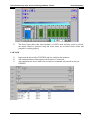
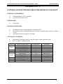
Federal Urdu University of Arts, Science & Technology Islamabad – Pakistan Electrical Engineering SEVENTH SEMESTER INDUSTRIAL ELECTRONICS BASIC ELECTRICAL & ELECTRONICS LAB DEPARTMENT OF ELECTRICAL ENGINEERING Prepared By: Checked By: Approved By: Engr. Asad Jamal Engr. M.Nasim Khan Dr.Noman Jafri Lecturer (Lab) Electrical, FUUAST-Islamabad Senior Lab Engineer Electrical, FUUAST-Islamabad Dean, FUUAST-Islamabad Industrial Electronics 1 Federal Urdu University of Arts, Science & Technology Islamabad – Pakistan Electrical Engineering Name: ____________________________________________ Registration No: ____________________________________ Roll No: ___________________________________________ Semester: _________________________________________ Batch: ____________________________________________ Industrial Electronics 2 Federal Urdu University of Arts, Science & Technology Islamabad – Pakistan Electrical Engineering C CO ON NT TE EN NT TSS Exp No 1 2 3 4 5 6 List of Experiments PHOTO-TRANSISTOR PHOTO INTERRUPTOR / PHOTO COUPLER / OBJECT DETECTOR CDS SENSOR SENSORS OBJECT DETECTOR DIGITAL HALL SENSOR ANALOG HALL SENSOR 7 TEMPERATURE SENSOR 8 HUMIDITY SENSOR 9 HALL CURRENT SENSOR / MAGNETIC DEVICE 10 PREXIMITY SENSOR 11 INTRODUCTION TO PLC’S 12 MOTOR START/STOP CONTROL PROGRAM 13 CONTROL SYSTEM FOR MOTORS WITH EMERGENCY BACKUP 14 WATER LEVEL CONTROL SYSTEM 15 MOTORS LOAD DISTRIBUTION CONTROL SYSTEM 16 TIMERS USING PLC Industrial Electronics 3 Federal Urdu University of Arts, Science & Technology Islamabad – Pakistan Electrical Engineering EXPERIMENT NO – 01 PHOTO-TRANSISTOR DISCRIPTION The circuit of figure is a light-controlled switch using a phototransistor. When incident light is absent, the resistance across C and E is high and the output voltage Vo is high. If incident light applied, the output voltage will reduce in response to incident illumination. Figure. A light-controlled switch. PROCEDURE 1. Complete the circuit of Figure on KL-64001 and KL-62001 breadboard 2. Connect the Vo1 to KL-62001 STATUS DISPLAY & DCV INPUT + and the E to -. 3. Complete the following connections on KL-62001. Industrial Electronics 4 Federal Urdu University of Arts, Science & Technology Islamabad – Pakistan SIGNAL SECTION MANUAL/SINGLE MANUAL CHIP SELECT TO SECTION AREA SELECT Electrical Engineering AREA SIGNAL → MANUAL/SINGLE CHIP GND 4. Switch power ON and the display should be ON. 5. Set STATUS DISPLAY & DCV MODE switch to DCV position and RANGE to 20V. 6. Cover the phototransistor window with hand and record the output voltage Vo1. Vo1 = ____________ V. 7. Lighten the phototransistor with fluorescent lamp and record the output voltage Vo1. Vo1 = ____________ V. 8. Adjust the distance between source and phototransistor and complete Table 1 Results Table 1 Distance 0cm 5cm 10cm 15cm 20cm 30cm 40cm 50cm Vo Industrial Electronics 5 Federal Urdu University of Arts, Science & Technology Islamabad – Pakistan Electrical Engineering EXPERIMENT NO – 2 PHOTO INTERRUPTOR / PHOTO COUPLER / OBJECT DETECTOR DISCRIPTION Figure shows an object detector using a fixed-distance photo coupler. In normal situation, the detector receives light signal from LED and the output voltage Vo is low. If an object passes through the window and blocks the light beam, the collector current Ic decreases and the output Vo rises to a high potential. The two inverters act as a wave shaper. Figure Object detector PROCEDURE 1. Complete the circuit of Figure on KL-64001 and KL-62001 breadboard 2. Connect the Vo2 to KL-62001 STATUS DISPLAY & DCV INPUT + and the - to GND. Connect the output CK to COUNTER input or Oscilloscope input. Industrial Electronics 6 Federal Urdu University of Arts, Science & Technology Islamabad – Pakistan 3. Electrical Engineering Complete the following connections on KL-62001. SECTION AREA SIGNAL TO SECTION SELECT MANUAL/SINGLE MANUAL → SELECT CHIP AREA MANUAL/SINGLE CHIP SIGNAL GND 4. Switch power ON and the display should be ON. 5. Set STATUS DISPLAY & DCV MODE switch to DCV position and RANGE to 20V. 6. In the absence of object between emitter and detector, measure and record the output voltage Vo2 = __________ V. 7. In the presence of object between emitter and detector, measure and record the output voltage Vo2 = __________ V. 8. Cut a sheet of paper to a pulse shape and move it between emitter and detector, and record the output waveform. Industrial Electronics 7 Federal Urdu University of Arts, Science & Technology Islamabad – Pakistan Electrical Engineering EXPERIMENT NO – 3 CDS SENSOR DESCRIPTION In this experimental circuit, we used CDS can change the light stronger or week to resistance value characteristics and get the purpose of light controlled circuit. As the Fig. 1 circuit the CDS is under the normal lighting operation. Adjusted the R1 make the LED 1 just from the dark to lighting, because the CDS resistance don’t have to much range, the voltage through CDS make R1 and R2 divided the voltage, let the Vb1 have a potential. This potential enough make Q1 turn on and make Vb2 potential get down. The Q2 is a PNP transistor, when B voltage (Vb) get down and lower to Emitter voltage (Vcc) a Vbe Bias, the Q2 will turn so the LED is lighting. Fig. 1 CDS light controlled circuit. Opposite, when you used the hand covered lighting of the CDS received, the CDS resistance will increased it make the Vb1 voltage get down suddenly. When Vb1 lower 0.7V, the Q1 cut off. It will make the Vb2 voltage increased, and Q2 Base voltage increases also make the Q2 cut off and LED turn off. It means the CDS received light, the LED1 will be lighting. If the CDS is not received the light, the LED also turn off. Industrial Electronics 8 Federal Urdu University of Arts, Science & Technology Islamabad – Pakistan Electrical Engineering PROCEDURE 1. Find the CDS connect terminal. 2. Used the meter measuring the CDS on the normal lighting, the resistance is __________ Ohm. 3. When used the hand covered CDS, what change about the resistance? __________ (increase or reduce?), in the same time the CDS resistance is __________ Ohm. 4. Get a 60W bulb lighting to CDS, what change about the resistance? a. __________ (increase or reduce?), in the same time the CDS resistance is __________ Ohm. 5. Can you used the CDS design a sample automatic lighting circuit? 6. Set the Module KL-64009 on the Trainer KL-62001. and connect the power source. 7. On the KL-62001 main Trainer ¡§SELECT¡¨ block, in the ¡§MANUAL/SINGLE CHIP¡¨ area, put the ¡§MANUAL¡¨ to ¡§GND¡¨. and in the ¡§STATUS DISPLAY & DCV, MODE¡¨ area, push on the ¡§DCV¡¨ and the range on the 20V. 8. Adjusting the R1, make the LED just on the lighting position. Used the voltmeter measuring the Vb1, Vb2, V023, 3 points voltage value and record on the Table. 9. Used the hand covered the lighting of the CDS received, even the CDS didn¡¦t received lighting but in this time the LED is turn ¡§ON¡¨ or ¡§OFF¡¨? MEASURING THE Vb1, Vb2, V023, the 3 points voltage and record on the Table. 10. If CDS and R1, R2 change the position, than when the CDS received the lighting which the LED1 is turn ¡§ON¡¨ or ¡§OFF¡¨? RESULTS STATUS Vb1 Vb2 V023 LED1 STATUS CDS lighting No-ighting CONCLUSION Industrial Electronics 9 Federal Urdu University of Arts, Science & Technology Islamabad – Pakistan Electrical Engineering EXPERIMENT NO – 4 SENSORS OBJECT DETECTOR PURPOSE OF EXPERIMENT 1) To work On KL-62001 Trainer. 2) To build Circuit on KL-64001. DISCRIPTION OF EXPERIMENTAL CIRCUITS Figure shows an object detector using a fixed-distance photocoupler. In normal situation, the detector receives light signal from LED and the output voltage Vo is low. If an object passes through the window and blocks the light beam, the collector current Ic decreases and the output Vo rises to a high potential. The two inverters act as a wave shaper. EXPERIMENTS AND RECORDS 1) Complete the circuit of Figure on KL-64001 and KL-62001 breadboard. 2) Connect the Vo2 to KL-62001 STATUS DISPLAY & DCV INPUT + and the - to GND. Connect the output CK to COUNTER input or Oscilloscope input. 3) Complete the following connections on KL-62001. SECTION AREA SIGNAL TO SECTION SELECT MANUAL/SINGLE MANUAL → SELECT CHIP AREA MANUAL/SINGLE CHIP SIGNAL GND 4) Switch power ON and the display should be ON. 5) Set STATUS DISPLAY & DCV MODE switch to DCV position and RANGE to 20V. Industrial Electronics 10 Federal Urdu University of Arts, Science & Technology Islamabad – Pakistan Electrical Engineering 6) In the absence of object between emitter and detector, measure and record the output voltage Vo2 = __________ V. 7) In the presence of object between emitter and detector, measure and record the output voltage Vo2 = __________ V. 8) Cut a sheet of paper to a pulse shape and move it between emitter and detector, and record the output waveform. Industrial Electronics 11 Federal Urdu University of Arts, Science & Technology Islamabad – Pakistan Electrical Engineering EXPERIMENT No. 5 DIGITAL HALL SENSOR DESCRIPTION: Figure 3 Digital Hall circuit shows the circuit. The block diagram of IC 3503 is shown in Figure 4 Block diagram of IC 3503. The internal power regulator Vref provides a constant-current to the Hall element X and a regulated voltage to amplifiers. The output transistor is an open-collector configuration which can sink the current up to 5mA. When a magnet is placed in close proximity with a magnetic field, as shown in Figure 5 The sensing method for Hall and magnet, its output is inversely proportional to the strength of; and the proximity to the magnetic field. To determine its output state (high or low), the output must be amplified by a differential amplifier. The amplified output is then send to a Schmitt latch, which determines the output state. To reverse the output state, a magnetic field of opposite polarity should be added. Refer to Figure 6 for the output voltage versus distance characteristics of IC 3503. PROCEDURE A. 1. Complete the circuit of Figure on KL-64001 and KL-62001 breadboard. 2. Connect the Vo4 to KL-62001 STATUS DISPLAY & DCV INPUT +. 3. Complete the following connections on KL-62001. SECTION AREA SIGNAL TO SECTION AREA MANUAL/SINGLE MANUAL/SINGLE SELECT MANUAL → SELECT CHIP CHIP SIGNAL 4. Switch power ON and the display should be ON. 5. Set STATUS DISPLAY & DCV MODE switch to DCV position and RANGE to 20V. Industrial Electronics GND 12 Federal Urdu University of Arts, Science & Technology Islamabad – Pakistan Electrical Engineering 6. In the absence of magnetic field, adjust the VR 10K to make the output voltage Vo=0V. 7. Move the magnet toward Hall sensor, observe and record the side of Hall having no reaction. 8. Move the magnet toward Hall sensor, observe and record the distance between magnet and Hall if a change occurs at the output. 9. Change the poles of magnet and repeat Steps 7 and 8. Digital hall IC 1. Set the Module KL-64001 on the Trainer KL-62001. 2. Connect the Vo3 in HALL-EFFECT Digital SENSOR area to the DCV INPUT + and switch power ON. 3. Move the magnet toward the Hall IC and try to find out which side the Hall has no response. 4. Record the distance between magnet and Hall if the change occurs at output. 5. Change the polarities of magnet and record the output variation of Hall IC. Industrial Electronics 13 Federal Urdu University of Arts, Science & Technology Islamabad – Pakistan Electrical Engineering EXPERIMENT NO - 6 ANALOG HALL SENSOR DESCRIPTION: The Hall sensor in Figure 1 is an analog element and the equivalent circuit is shown in Figure 2 Since the bridge arms are not balance, the 13K resistor is for the compensation. The VR 10K in Figure 1 acts as an adjuster for the offset of differential amplifier. Figure 1. Analog Hall sensor circuit. Figure 2. The equivalent circuit of analog Hall sensor. Fig 1 Analog Hall IC shows a Hall detector using an analog Hall IC LT110. The output of this Hall element is directly proportional to the distance from the magnetic field. The analog signal is amplified by the differential amplifier U3. Industrial Electronics 14 Federal Urdu University of Arts, Science & Technology Islamabad – Pakistan Electrical Engineering PROCEDURE: A. 1. Complete the circuit of Figure on KL-64001 and KL-62001 breadboard. 2. Connect the Vo4 to KL-62001 STATUS DISPLAY & DCV INPUT +. 3. Complete the following connections on KL-62001. SECTION AREA SIGNAL TO SECTION AREA MANUAL/SINGLE MANUAL/SINGLE SELECT MANUAL → SELECT CHIP CHIP SIGNAL GND 4. Switch power ON and the display should be ON. 5. Set STATUS DISPLAY & DCV MODE switch to DCV position and RANGE to 20V. 6. In the absence of magnetic field, adjust the VR 10K to make the output voltage Vo=0V. 7. Move the magnet toward Hall sensor, observe and record the side of Hall having no reaction. 8. Move the magnet toward Hall sensor, observe and record the distance between magnet and Hall if a change occurs at the output. 9. Change the poles of magnet and repeat Steps 7 and 8.\ Industrial Electronics 15 Federal Urdu University of Arts, Science & Technology Islamabad – Pakistan Electrical Engineering Analog hall IC 1. Set the Module KL-64001 on the Trainer KL-62001. 2. Connect the Vo4 in HALL-EFFECT Analog SENSOR area to the DCV INPUT + and switch power ON. 3. Move the magnet toward the Hall IC and try to find out which side the Hall has non response. 4. Record the distance between magnet and Hall if the change occurs at output. 5. Change the polarities of magnet and record the output variation of Hall IC. Industrial Electronics 16 Federal Urdu University of Arts, Science & Technology Islamabad – Pakistan Electrical Engineering EXPERIMENT NO - 7 TEMPERATURE SENSOR DESCRIPTION The AD590 is an excellent sensor for temperature-to-current conversion due to its good linearity with a transduction ratio of 1(A/((K. The circuit of Figure 1 is the AD590 transduction circuit with two different transduction outputs, the 10mV/((K at U1 PIN6 and the 100mV/¢J at Vo15. The U1 acts as a voltage follower. The output of U1 can obtain the voltage of 10mV/((K by adjusting the R2 for R2+R3=10K(. In many applications, the Celsius scale is more convenient than absolute temperature. The relationship of these two temperature scales is ((K =((C+273.2, and 273.2((K =0((C. In other words, if the temperature is at 273.2((K (0((C), the output voltages at Vf1 and U1 should be 2.732V and 0V, respectively. In order to yield the 2.732V stabilized voltage, a voltage regulator which consist of R6, CR1, R7, R8, R9 and U3 is used. Figure 1. AD590 transducer circuit. A digital thermometer shown in Figure 2 is built with the AD590 transducer module and the Industrial Electronics 17 Federal Urdu University of Arts, Science & Technology Islamabad – Pakistan Electrical Engineering 7135 A/D converter. Since the transduction output of the AD590 transducer is 100mV/¢J, such that the full-scale voltage of the A/D converter must be set to 20V. Figure 2. Digital thermometer. PROCEDURE A. Characteristics and transduction circuit of the AD590 1. Place Module KL-64005 Block 15 on the Trainer KL-62001. 2. Measure the resistance between U1 pin3 GND with the DMM and adjust the R2 for the resistance value of 10KΩ. 3. Adjust the R8 to make Vf1=2.732V. 4. Put the AD590 in the Thermostatic Container. (The pins of AD590 must be isolated from water) Measure and record the output voltages at U1 pin6 and Vo15 for each temperature setting in Table 1. 5. From Table 1 the voltage difference between U1 pin6 and Vo15=_______ V. 6. Construct the conversion curve of AD590 transducer using data in Table 1. 7. Review the curve in Step 6, calculate and record the temperature-to-voltage transduction ratio = _____________ mV/¢J. B. Digital thermometer 1. Place module KL-64005 on KL-62001. 2. Repeat Steps 2 to 5 from section A. Industrial Electronics 18 Federal Urdu University of Arts, Science & Technology Islamabad – Pakistan Electrical Engineering 3. Set the MODE switch to the SENSOR position, the RANGE switch to the ¢J position and connect MANUAL (SELECT area) to GND on the Module KL-62001. 4. Connect the Vo15 on KL-64005 to the DCV INPUT+ on KL-62001. 5. Insert the AD590 into the Thermostatic Container.Read and record the readout for each temperature setting in Table 2. 6. Compare the settings with the readouts. C. Computer interface and control Figure shows the functional blocks of module KL-62001. The transducer output (0 to +5VDC) applies to inputs of the 12-bit A/D converter, and then is converted to digital signals to the PIO chip or the single-chip microcomputer 8031 according to control signals. The PIO chip is a interface for transmitting the digital signals to a buffer card in a personal computer. The RS-232 is a communication-interface for communication between the single-chip 8031 and serial ports of the personal computer. Refers to the KL-62001 USER'S MANUAL for details. KL-62001 Figure. Functional diagram of KL-62001. 1. Complete the connections as follows: SECTION Industrial Electronics AREA SIGNAL TO SECTION AREA SIGNAL 19 Federal Urdu University of Arts, Science & Technology Islamabad – Pakistan SELECT MANUAL / SINGLE CHIP SINGLE CHIP OUT CONTROL & EPROM A/ D CONTROL CONVERTER A/ D CONTROL CONVERTER CHIP → SELECT 1 → AMPLIFIER Electrical Engineering MANUAL / SINGLE CHIP ALARM AMPLIFIER A /D IN→ KL-64005 Vo15 GND → KL-64005 GND GND SIN IN 2. Using 25-pin cable, connect the RS-232 interface to any serial port of personal computer. 3. Set the AD590 Transducer Module KL-64005 on the Trainer KL-62001. 4. Repeat Steps 2 to 3 from section A. 5. Set the DIP switches to the value of 4095. 6. Turn on KL-62001. 7. Complete Table 3. 8. When the temperature exceeds the setting, the potential at OUT CONTROL pin4 should be LOW and the alarm buzzer is turned on. Previous Steps are used to display the temperature values of the AD590 transducer through the single-chip microcomputer. 9. Connect the SINGLE CHIP & EPROM OUT CONTROL CTRL to the GND. 10. Boot the computer using the KL-62001 disk. At A> type CD BASIC <ENTER> Then type (YOURBASIC) <ENTER> At OK type LOAD "KLPLOTER <ENTER> At OK type RUN <ENTER> 11. The screen will display Select Monochrome or Color display : (M/C) (M=monochrome; C=color; default=C) Select RS232 ON COM1 or COM2 : (1/2) (1=COM1; 2=COM2; default=COM2) 12. After your selections, the screen shows 9 functions: 1. Acquire Data Industrial Electronics 20 Federal Urdu University of Arts, Science & Technology Islamabad – Pakistan Electrical Engineering 2. Load Data 3. Save Data 4. Plot Data 5. Sample Times ⇒ 10000 6. Range(Voltage) .25 to 5 ⇒ 5 7. Sample Rate HR:MN:SC ⇒ MAX 8. Print Data 9. EXIT 13. Select function 1 by typing. (i) 1 <ENTER> (b) Change the temperature values and observe the temperature curve on the screen. (1V = 10¢J) (c) If the screen displays the error message " Device Timeout in 600 ", please (d) retry from Step 12 for a correct selection of the RS232 port. 14. Type 9 <ENTER> to exit. RESULTS Table 1 Temperature(¢J) U1 pin6 (V) Vo15 (V) 30Ξ′ 40Ξ′ 50Ξ′ 60Ξ′ 70Ξ′ 80Ξ′ 90Ξ′ 100Ξ′ Table 2 Industrial Electronics 21 Federal Urdu University of Arts, Science & Technology Islamabad – Pakistan Temperature(¢J) Readout 30 40 50 60 70 Electrical Engineering 80 90 100 Table 3 DIP-switch Settings 0819 (10¢J) 1638 (20¢J) 2457 (30¢J) 3276 (40¢J) 4095 (50¢J) KL-62001 readout Temperature(¢J) OUT CONTROL pin1 OUT CONTROL pin4 KL-64005 Vo15 volts Industrial Electronics 22 Federal Urdu University of Arts, Science & Technology Islamabad – Pakistan Electrical Engineering EXPERIMENT NO. 8 HUMIDITY SENSOR DESCRIPTION The circuit of Figure 1 is a humidity transducer circuit for this experiment. This circuit consists of four sections: The first section is an oscillator consisted of U5 and U6.The U6, Wein oscillator, generates a sine wave. The U5 acts as an amplitude limiter to limit the sine wave at 250 Hz and 0.5 Vrms. The second section serves amplification, filtering, and rectification. It consists of U4, C1, and CR2. The magnitude of negative output is proportional to sensed humidity. The R17 is for gain adjustment and the R14 is for zero level calibration. Figure 2 shows the characteristic of humidity sensor. Figure 1. Humidity transducer circuit Industrial Electronics 23 Federal Urdu University of Arts, Science & Technology Islamabad – Pakistan Electrical Engineering Figure 2. Characteristic of HOS201. HYGROMETER In Figure 1, we measure the output voltage of Vo16 using DMM or AD converter. Using DMM, the voltage reading must divide by 100 mV to obtain the value of humidity. Using AD converter, the readout represents the value of humidity. The operating range of HOS201 is from 55 to 100 %RH and a tolerance of ©ϒ3 %RH. PROCEDURE A. Basic measurement 1. Set the Humidity Transducer Module KL-64005 Block 16 on the Trainer KL-62001. Supply the power. 2. Using scope, measure and record the signal at Vf2. f = ____________ Hz, Vp-p = ___________ V. 3. Using scope, measure and record the signal at SENSOR16. f = ____________ Hz, Vp-p = ___________ V. B. Impedance measurement 1. Connect the DMM probes to HOS201 lead wires. Industrial Electronics 24 Federal Urdu University of Arts, Science & Technology Islamabad – Pakistan Electrical Engineering 2. Set humidity disk with water, hygrometer and HOS201 in the Thermostatic. 3. Complete Table 1 using the fan and water. 4. Plot the impedance vs. humidity curve using the data in Table 1. 5. Compare the curve in Step 4 to the curve in Figure 2 and explain the difference. 6. Compare the humidified impedance to the dehumidified impedance and explain the difference. C. Conversion voltage measurement 1. Set the Humidity Transducer Module KL-64005 Block 16 on the Trainer KL-62001. supply the power. 2. Connect the HUMIDITY SENSOR leads to SENSOR IN. 3. Repeat Step 2 in experiment B. 4. Complete Table 2. 5. Plot V sensor16 vs. humidity, Vu4, pin6 vs. humidity, and Vo16 vs. humidity curves. D. Computer control 1. Complete the following connections: SECTION AREA SINGLE CHIP & OUT CONTROL EPROM SIGNAL TO SECTION 1 → AMPLIFIER AREA SIGNAL ALARM SIN IN KL-64005 Vo16 → POTENTIO- METER VR1 KL-64005 GND → POTENTIO- METER VR3 POTENTIOMETER POTENTIOMETER VR2 → A/D CONVERTER VR3 → SELECT MANUAL/SINGLE CHIP CONTROL A/D IN GND 2. Repeat Steps 1 and 2 in experiment C. 3. Complete Table 3. 4. Connect the SINGLE CHIP & EPROM OUT CONTROL CTRL to the GND. This step performs the data communications between the transducer circuit and the personal computer via the RS-232 port. Industrial Electronics 25 Federal Urdu University of Arts, Science & Technology Islamabad – Pakistan Electrical Engineering 5. Follow the steps for the RS-232C control in experiment temperature(AD590) computer control and proceed the following steps. 6. (Note: 1V=10%RH) RESULTS Table 1 40% 45% 50% 55% 60% 65% 70% 75% 80% 85% 90% 95% RH RH RH RH RH RH RH RH RH RH RH RH Humidity Humidified impedance Dehumidified impedance Table 2 Humidity 40% 45% 50% 55% 60% 65% 70% 75% 80% 85% 90% 95% RH RH RH RH RH RH RH RH RH RH RH RH V sensor16 V u4,pin6 Vo16 Table 3 DIP-switch settings 0082 10%RH 0164 20%RH 0246 30%RH 0328 40%RH 0409 50%RH 0491 60%RH 0573 70%RH 0655 80%RH 0737 0819 90%RH 100%RH KL-62001 Readout Temperature (¢J) OUT CONTROL pin1 OUT CONTROL pin4 KL-64005 Vo16 Table 4 DIP-switch settings KL-62001 Readout Temperature (¢J) OUT CONTROL pin1 OUT CONTROL pin4 KL-64005 Vo16 Industrial Electronics 26 Federal Urdu University of Arts, Science & Technology Islamabad – Pakistan Electrical Engineering EXPERIMENT NO- 9 HALL CURRENT SENSOR / MAGNETIC DEVICE DESCRIPTION The SY-03 Characteristics: PARAMETER SAMBOL Nominal input If current(F.S) Linear range Output voltage Vh Zero current offset Vo Linearity ρ Power supply Vcc Rating Resoponse time Trr Thermal characteristics Hystersis error Insulation resistance Operation temperature Storage temperature Ta Ts CHARACTERISTICS ©ϒ 3A DC 0~©ϒ 6A DC 4V ©ϒ 1% at If within ©ϒ 0.04V at If = 0 within ©ϒ 1% of Vh at If = F.S ©ϒ 15V DC within ©ϒ 5% 3 µ S Max. at di/dt = 100A / µ S within ©ϒ 0.1% / ¢J (within ©ϒ0.08% / ¢J Typical) at RL=10KΩ within 0.02V at If = 100A → 0 500MΩ Min.at 500V DC -10¢J ~ +70¢J -15¢J ~ +85¢J From the charateristics we know the input current (If) is 0~3A, so that: output voltage (Vh) is 0~4V, for the proportion of the value of output voltage to input current, so that: Industrial Electronics 27 Federal Urdu University of Arts, Science & Technology Islamabad – Pakistan Electrical Engineering Vo1 = -(R2+R9) / R1¡DVi = -0.75¡D(4V) = -3V Vo = -R5 / R4¡DVo1 = -(10K / 10K)¡D(-3V) = 3V When the input current change from 0~3A, output voltage is 0~3V; R3, R6 are DC offsetadjustment. The input current is 0, adjusting is knob make the output voltage is 0. PROCEDURE 1. On the KL-62001 main Trainer ¡§SELECT¡¨ block, in the ¡§MANUAL/SINGLE CHIP¡¨ aera, put the ¡§MANUAL¡¨ to ¡§GND¡¨. and in the ¡§STATUS DISPLAY & DCV, MODE¡¨ area, push on the ¡§DCV¡¨ and the range on the 20V. The main unit provides the power supply to the module. 2. Turn on the power supply, put the voltage in 10V, current in 100mA. Connecting the main unit power supply to KL-64008 Vin+ and Vin-. 3. Kept the voltage in same, adjust the current to 0 mA. 4. Adjust R3, make Vo1 output is 0V, and adjust R6 make Vo21 output voltage is 0V. 5. Change the power supply current to 1A, adjust the R9 make Vo21 voltage to 1V. 6. Above adjustment is for calibration voltage output, to make it is an calibrated current detector. 7. Change the terminals of power supply to any other current circuit, willknow the circuit current are how many? (Attention the current can not over 3A) Industrial Electronics 28 Federal Urdu University of Arts, Science & Technology Islamabad – Pakistan Electrical Engineering EXPERIMENT No. 10 PREXIMITY SENSOR DESCRIPTION As Fig. 1 is used the capacititive type proximity switches for the experimental circuit Fig. 1 Capacititive type proximity switches SPECIFICATION: D.C.Current: 10--30VDC Max. Ripple: 10% Real Dis.: <80%(Sr) Magnetic hysteresis: <15%(Sr) Accurancy: <5% The sensor is on the ¡§HIGH¡¨ position when they are no metal approach, through the U3-a Schmitt reverser the Vo22 point is low position that why the buzzer no alarm. When the metal objector near the sensor, the LED turn on and output become low level, through the reverser become high position than the transistor turn on, the buzzer alarm. Industrial Electronics 29 Federal Urdu University of Arts, Science & Technology Islamabad – Pakistan Electrical Engineering PROCEDURE 1. Set the Module KL-64008 on the Trainer KL-62001. and connect the power source. 2. Plug-in the capacitive proximity switch to the module, Switch the power on. 3. When no metal approach the proximity switch, what voltage on the output and Vo22? 4. When the metals approach the proximity switch, how long the distance the buzzer will be alarm? Industrial Electronics 30 Federal Urdu University of Arts, Science & Technology Islamabad – Pakistan Electrical Engineering EXPERIMENT NO – 11 INTRODUCTION TO PLC’S BASICS A programmable logic controller (PLC) or programmable controller is a digital computer used for automation of electromechanical processes,such as control of machinery on factory assembly lines, amusement rides, or lighting fixtures. PLCs are used in many industries and machines. Unlike generalpurpose computers, the PLC is designed for multiple inputs and output arrangements, extended temperature ranges, immunity to electrical noise, and resistance to vibration and impact. Programs to control machine operation are typically stored in battery-backed or non-volatile memory. A PLC is an example of a real time system since output results must be produced in response to input conditions within a bounded time, otherwise unintended operation will result The main difference from other computers is that PLCs are armored for severe conditions (such as dust, moisture, heat, cold) and have the facility for extensive input/output (I/O) arrangements. These connect the PLC to sensors and actuators. PLCs read limit switches, analog process variables (such as temperature and pressure), and the positions of complex positioning systems. Some use machine vision. On the actuator side, PLCs operate electric motors, pneumatic or hydraulic cylinders, magnetic relays, solenoids, or analog outputs. The input/output arrangements may be built into a simple PLC, or the PLC may have external I/O modules attached to a computer network that plugs into the PLC. PLCs are well-adapted to a range of automation tasks. These are typically industrial processes in manufacturing where the cost of developing and maintaining the automation system is high relative to the total cost of the automation, and where changes to the system would be expected during its operational life. PLCs contain input and output devices compatible with industrial pilot devices and controls; little electrical design is required, and the design problem centers on expressing the desired sequence of operations. PLC applications are typically highly customized systems so the cost of a packaged PLC is low compared to the cost of a specific custom-built controller design. On the other hand, in the case of mass-produced goods, customized control systems are economic due to the lower cost of the components, which can be optimally chosen instead of a "generic" solution, and where the non-recurring engineering charges are spread over thousands or millions of units. A microcontroller-based design would be appropriate where hundreds or thousands of units will be produced and so the development cost (design of power supplies, input/output hardware and necessary testing and certification) can be spread over many sales, and where the end-user would not need to alter the control. Automotive applications are an example; millions of units are built each year, and very few end-users alter the programming of these controllers. However, some specialty vehicles such as transit busses economically use PLCs instead of custom-designed controls, because the volumes are low and the development cost would be uneconomic. Very complex process control, such as used in the chemical industry, may require algorithms and performance beyond the capability of even high-performance PLCs. Very high-speed or precision controls may also require customized solutions; for example, aircraft flight controls. Programmable controllers are widely used in motion control, positioning control and torque control. Some manufacturers produce motion control units to be integrated with PLC so that G-code (involving Industrial Electronics 31 Federal Urdu University of Arts, Science & Technology Islamabad – Pakistan Electrical Engineering a CNC machine) can be used to instruct machine movements.[citation needed] Industrial Electronics 32 Federal Urdu University of Arts, Science & Technology Islamabad – Pakistan Industrial Electronics Electrical Engineering 33 Federal Urdu University of Arts, Science & Technology Islamabad – Pakistan Industrial Electronics Electrical Engineering 34 Federal Urdu University of Arts, Science & Technology Islamabad – Pakistan Industrial Electronics Electrical Engineering 35 Federal Urdu University of Arts, Science & Technology Islamabad – Pakistan Electrical Engineering EXPERIMENT NO – 12 MOTOR START/STOP CONTROL PROGRAM PURPOSE OF EXPERIMENT 1) 2) 3) Understand motor’s starting principle using PLC. Learn about I/O MAP of PLC. Understand the structure and principle of PLC SIMULATOR PREPARATION 1) 2) PC (FXGPWIN Installed) PC (GMWIN Installed) RELATED KNOWLEDGE 1) 2) 3) One should be able to understand motor’s starting method. One should be able to understand basic sequence circuit. One should be able to design PLC I/O MAP. ACTIVATION CONDITION 1) 2) 3) 4) Build motor’s start circuit by using two input switches (start, stop). (Output consists of output coil for electronic contact maker, operation lamp, and stop lamp.) Initially stop lamp must glow. If start input switch is turned on, motor gets started, and then operation lamp turns on whereas stop lamp turns off. If one turns on stop lamp during operation, motor stops, and lamp turns on, and operation lamp turns off. PLC I/O MAP is configured below. Section Inputs Outputs Indirect Variable Name START_SWITCH STOP_SWITCH MOTOR OPERATION _LAMP STOP_LAMP Comments Push Switch S-2 Push Switch S-3 MOTOR-1 (-) Lamp L-2 Lamp L-1 PROGRAM PRACTICE 1) 2) 3) Execute the GMWIN and open the Project window and the program window. Write a program using PLC I/O MAP Write ladder program as shown below. Industrial Electronics 36 Federal Urdu University of Arts, Science & Technology Islamabad – Pakistan Electrical Engineering EXECUTION OF PROGRAM (USING SIMULATOR) 1) 2) To verify what was mentioned above, one uses a simulator, which is characteristic of GLOFA t perform an experiment to check whether there is any abnormality in the circuit and its activation. Simulator starts when one clicks the icon on Basic tool bar. When one clicks on this icon, firstly following window opens If one clicks OK than simulator starts and we can use inputs and outputs of simulator to monitor our program. Industrial Electronics 37 Federal Urdu University of Arts, Science & Technology Islamabad – Pakistan 3) Electrical Engineering The above figure shows that when simulator is in RUN mode and start switch is pressed, the output related to operation lamp and motor status are activated which means that program is working properly. LAB TASK 1) 2) 3) Implement the above lab in FXGPWIN and also configure the hardware. Also mentioned that in what sequence the hardware is connected. Also implement the above ladder with set and reset command as discussed in class (in GMWIN). Industrial Electronics 38 Federal Urdu University of Arts, Science & Technology Islamabad – Pakistan Electrical Engineering LADDER DIAGRAM WORKING DESCRIPTION CONCLUSION Industrial Electronics 39 Federal Urdu University of Arts, Science & Technology Islamabad – Pakistan Electrical Engineering EXPERIMENT NO – 13 CONTROL SYSTEM FOR MOTORS WITH EMERGENCY BACKUP PURPOSE OF EXPERIMENT 1) 2) Understand motor’s PLC Commands. Learn about I/O MAP of PLC. PREPARATION 1) FXGP-WIN RELATED KNOWLEDGE 1) 2) 3) One should be able to understand basic commands of PLC. One should be able to understand the basics of motors controlling logic and basic sequence circuit.. One should be able to design PLC I/O MAP. ACTIVATION CONDITION 1) 2) Build motor’s start/stop circuit by using four input switches (operation, stop). PLC I/O MAP is configured below. Section Inputs Outputs Industrial Electronics Indirect Variable Name START_SWITCH_M1 STOP_SWITCH_M1 START_SWITCH_M2 STOP_SWITCH_M2 EMERGENCY MOTOR_M1 M1 _LAMP MOTOR_M2 M2 _LAMP EMERGENCY_LAMP BUZZER I/O Allocation X.0 X.1 X.2 X.3 X.4 Y0 Y2 Y1 Y3 Y4 Y5 Comments Switch S-1 Switch S-2 Switch S-3 Switch S-4 Switch S-4 MOTOR-1 (-) Lamp L-1 Lamp L-2 MOTOR-1 (-) Lamp L-3 Buzzer B-1 40 Federal Urdu University of Arts, Science & Technology Islamabad – Pakistan Electrical Engineering PROGRAM PRACTICE 1) 2) 3) Execute the FXGP-WIN and open the Project window and the program window. Write a program using PLC I/O MAP Write ladder program as shown below. EXECUTION OF PROGRAM (USING SIMULATOR) Execute the program by converting and then writing to the plc. Follow the steps used in the previous lab. SUMMARY OF LOGIC USED/PROGRAM SUMMARY Industrial Electronics 41 Federal Urdu University of Arts, Science & Technology Islamabad – Pakistan Electrical Engineering EXPERIMENT NO – 14 WATER LEVEL CONTROL SYSTEM PURPOSE OF EXPERIMENT 3) 4) Understand motor’s PLC Commands. Learn about I/O MAP of PLC. PREPARATION 2) FXGP-WIN RELATED KNOWLEDGE 4) 5) 6) One should be able to understand basic commands of PLC. One should be able to understand the basics of motors controlling logic and basic sequence circuit.. One should be able to design PLC I/O MAP. ACTIVATION CONDITION 3) 4) Build motor’s start/stop circuit by using four input switches (operation, stop). PLC I/O MAP is configured below. Section Indirect Variable Name I/O Allocation Comments Inputs Outputs PROGRAM PRACTICE 4) 5) 6) Execute the FXGP-WIN and open the Project window and the program window. Write a program using PLC I/O MAP Write ladder program as shown below. Industrial Electronics 42 Federal Urdu University of Arts, Science & Technology Islamabad – Pakistan Electrical Engineering LADDER DIAGRAM WORKING DESCRIPTION CONCLUSION Industrial Electronics 43 Federal Urdu University of Arts, Science & Technology Islamabad – Pakistan Electrical Engineering EXPERIMENT NO – 15 MOTORS LOAD DISTRIBUTION CONTROL SYSTEM PURPOSE OF EXPERIMENT 5) 6) Understand motor’s PLC Commands. Learn about I/O MAP of PLC. PREPARATION 3) FXGP-WIN RELATED KNOWLEDGE 7) 8) 9) One should be able to understand basic commands of PLC. One should be able to understand the basics of motors controlling logic and basic sequence circuit.. One should be able to design PLC I/O MAP. ACTIVATION CONDITION 5) 6) Build motor’s start/stop circuit by using four input switches (operation, stop). PLC I/O MAP is configured below. Section Indirect Variable Name I/O Allocation Comments Inputs Outputs LADDER DIAGRAM Industrial Electronics 44 Federal Urdu University of Arts, Science & Technology Islamabad – Pakistan Electrical Engineering WORKING DESCRIPTION CONCLUSION Industrial Electronics 45 Federal Urdu University of Arts, Science & Technology Islamabad – Pakistan Electrical Engineering EXPERIMENT NO – 16 TIMERS USING PLC A driven coil sets internal PLC contacts (NO and NC contacts available). Various timer resolutions are possible, from 1 to 100 msec, but availability and quantity vary from PLC to PLC. Selectable timers taken from the main range of 100 msec timers. Timers operate by counting clock pulses (1, 10 and 100 msec). The timer output contact is activated when the count data reaches the value set by the constant K. The overall duration or elapsed time, for a timers operation cycle, is calculated by multiplying the present value by the timer resolution, i.e. A 10 msec timer with a present value of 567 has actually been operating for: 567 10 msec 567 0.01 sec = 5.67 seconds Timers can either be set directly by using the constant K to specify the maximum duration or indirectly by using the data stored in a data register (ex. D). For the indirect setting, data registers which are battery backed/ latched are usually used; this ensures no loss of data during power down situations. If however, the voltage of the battery used to perform the battery backed service, reduces excessively, timer malfunctions may occur. On certain programmable controllers, driving a special auxiliary coil redefines approximately half of the 100 msec timers as 10 msec resolution timers. The following PLC’s and timers are subject to this type of selection. - FX0, FX0S driving M8028 ON, timers T32 to 55 (24 points) are changed to 10 msec resolution. - FX0N driving M8028 ON, timers T32 to 62 (31 points) are changed to 10 msec resolution. Industrial Electronics 46 Federal Urdu University of Arts, Science & Technology Islamabad – Pakistan Electrical Engineering PROGRAM FOR OPERATING A BUZZER FOR 1ms 1. Build buzzer’s start/stop circuit by using one input switch, a 1ms timer and a buzzer as an output. 2. Execute the FXGP-WIN and open the Project window and the program window. 3. Write ladder program as shown below. PROGRAM FOR TURNING A DEVICE ON/OFF AT A CONTROLLED RATE. In this example, the Output Y0 will be ON for 1 sec and then OFF for 1 sec. It will be used to describe how a PLC ladder can be produced, modified and tested. Then using a Mitsubishi FX2NPLC, the program will be downloaded, run and monitored The ladder diagram for the circuit and its explanation is given below. 1. Line 0 (a) On closing the input switch X0, the timer T0 will be enabled via the normally closed contact of timer T1. (b) Timer T0 will now start timing out, and after 1 sec, the Timer will operate. This means: (i) Any T0 normally open contacts -jj-, will close. (ii) Any T0 normally closed contacts -j / j-, will open. 2. Lines 5 and 9 There are two T0 contacts, which are both normally open, therefore both of them will close, causing the following to occur: (a) Timer T1 will become enabled and start timing out. (b) Output Y0 will become energized, i.e. output Y0 will turn ON. 3. Line 5 After timer T1 has been energized for 1 sec, it will also operate and its normally closed contact will open, causing Timer T0 to dropout. 4. With Timer T0 dropping-out, its normally open contact will now re-open causing: (a) Timer T1 to dropout even though T1 has just timed out. Industrial Electronics 47 Federal Urdu University of Arts, Science & Technology Islamabad – Pakistan Electrical Engineering (b) Output Y0 to become de-energized, i.e. output Y0 will turn OFF. 5. Hence it can be seen that timer T1 is part of a ‘cut-throat’ circuit in that when it does time out, it immediately de-energizes itself. 6. With timer T1 dropping-out, its normally closed contact will close, and for as long as input X0 is closed, the operation will be constantly repeated. 7. Line 9 Hence the output Y0 will be continuously OFF for 1 sec and then ON for 1 sec. LAB ASSIGNMENT Design a system controlling three motors with conditions: 1. All the three motors should operate for 1 second. 2. When motor 1 is on, the others two should be off i.e. only one motor should operate at a time. CONCLUSION Industrial Electronics 48