1
Freescale Semiconductor
User’s Guide
Document Number: FRDMKL43ZUG
Rev. 0, 7/2014
FRDM-KL43Z User’s Guide
1
FRDM-KL43Z overview
The Freescale Freedom development platform is a set of
software and hardware tools for evaluation and
development. It is ideal for rapid prototyping of
microcontroller-based applications. The Freescale
Freedom KL43Z hardware, FRDM-KL43Z, is a simple,
yet sophisticated design featuring a Kinetis L series
microcontroller, built on the ARM® Cortex™-M0+
core.
FRDM-KL43Z can be used to evaluate the KL43, KL33,
KL27, and KL17 Kinetis L series devices. It features a
MKL43Z256VLH4 which has a maximum operating
frequency of 48 MHz, 256 KB of flash memory, 32 KB
RAM, 16 KB ROM (with Kinetis bootloader), a
full-speed device USB controller, segment LCD
controller, and many analog and digital peripherals. The
FRDM-KL43Z hardware is form-factor compatible with
the Arduino™ R3 pin layout, providing a broad range of
expansion board options. The on-board interfaces
include a 4-digit segment LCD, a 3-axis digital
© 2014 Freescale Semiconductor, Inc. All rights reserved.
Contents
1
2
3
4
5
FRDM-KL43Z overview . . . . . . . . . . . . . . . . . . . . . . . . .
Reference documents . . . . . . . . . . . . . . . . . . . . . . . . . . .
Getting started . . . . . . . . . . . . . . . . . . . . . . . . . . . . . . . . .
FRDM-KL43Z hardware overview . . . . . . . . . . . . . . . . . .
FRDM-KL43Z hardware description . . . . . . . . . . . . . . . .
5.1 Power supply . . . . . . . . . . . . . . . . . . . . . . . . . . . . . .
5.2 Serial and debug adapter (OpenSDA). . . . . . . . . . .
5.3 MKL43Z256 microcontroller . . . . . . . . . . . . . . . . . .
1
2
2
2
4
4
6
8
Reference documents
accelerometer, magnetometer, capacitive touch slider (not directly connected because there is no TSI
module on the chip—only software TSS can be used with GPIO method), and ambient light sensor.
The FRDM-KL43Z features the Freescale open standard embedded serial and debug adapter known as
OpenSDA. This circuit offers several options for serial communications, flash programming, and run-control
debugging.
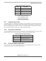
2
Reference documents
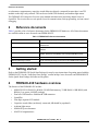
Table 1 provides a list of reference documents for the FRDM-KL43Z hardware. All of these documents
are available online at www.freescale.com/FRDM-KL43Z.
Table 1. FRDM-KL43Z reference documents
File name
3
Description
FRDM-KL43Z Quick Start Package
Quick Start Guide and supporting files for getting started with the
FRDM-KL43Z.
FRDM-KL43Z User’s Guide
This document—overview and detailed information for the FRDM-KL43Z
hardware.
FRDM-KL43Z Pinouts
Spreadsheet of pin connections for all MCU pins. Includes pinout for the I/O
headers, Arduino R3 compatibility chart, and OpenSDA MCU pinout.
FRDM-KL43Z Schematics
PDF schematics for the FRDM-KL43Z hardware.
FRDM-KL43Z Design Package
Zip file containing all design source files for the FRDM-KL43Z hardware.
OpenSDA User’s Guide
Overview and instructions for use of the OpenSDA embedded.
Getting started
Refer to the FRDM-KL43Z Quick Start Package for step-by-step instructions for getting started with the
FRDM-KL43Z. See the “Jump Start Your Design” section on http://www.freescale.com/FRDM-KL43Z
for the Quick Start Package and software lab guides.
4
FRDM-KL43Z hardware overview
The features of the FRDM-KL43Z include:
• MKL43Z256VLLZ4 MCU (48 MHz, 256 KB flash memory, 32 KB RAM, 16 KB ROM (with
Kibble), Low power, 64LQFP package)
• Dual role USB interface with mini-B USB connector
• OpenSDA
• Four-digit segment LCD module
• Capacitive touch slider (not directly connected; 0R should be populated)
• Ambient light sensor
• MMA8451Q accelerometer
• MAG3110 magnetometer
FRDM-KL43Z User’s Guide, Rev. 0
22
Freescale Semiconductor
FRDM-KL43Z hardware overview
•
•
•
•
•
•
•
2 user LEDs
2 user push buttons
Flexible power supply options – USB, coin cell battery, external source
Battery-ready, power-measurement access points
Easy access to MCU I/O via Arduino R3 compatible I/O connectors
Programmable OpenSDA debug interface with multiple applications available including:
— Mass storage device flash programming interface
— P&E Debug interface provides run-control debugging and compatibility with IDE tools
— CMSIS-DAP interface: new ARM standard for embedded debug interface
— Data logging application
Arduino R3 compatibility
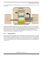
Figure 1 shows a block diagram of the FRDM-KL43Z design. The primary components and their
placement on the hardware assembly are pointed out in Figure 2.
,2+HDGHU
0LQL%
86%
9/'2
.LQHWLV .6HULHV
.';9)0
SLQ
'HEXJ
V/&'
8$57
.LQHWLV / 6HULHV
./=9/+
63,*3,2!6:'
766
5(6(7
2SHQ6'$
(OHFWURGHV
V/&'
0LQL%
86%
V/&'
7KHUPLVWRU
7KHUPLVWRU
SLQ
'HEXJ
,&,QHUWLDO
6HQVRU
,2+HDGHU
,2+HDGHU
Figure 1. FRDM-KL43Z block diagram
FRDM-KL43Z User’s Guide, Rev. 0
Freescale Semiconductor
3
FRDM-KL43Z hardware description
&DSDFLWLYH
7RXFK6OLGHU
6:
6:
'LJLWV/&'
/LJKW
VHQVRU
5HG
/('
- ,2
+HDGHU
- ,2
+HDGHU
- ,2
+HDGHU
*UHHQ
/('
0DJQHWRPHWHU
./=
0$*
- ,2
+HDGHU
$FFHOHURPHWHU
00$4
./
6:'
2SHQ6'$
'HEXJ
5HVHW
./86%
2SHQ6'$86%
͘
Figure 2. FRDM-KL43Z main components placement.
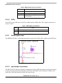
5
FRDM-KL43Z hardware description
5.1
Power supply
There are multiple power supply options on the FRDM-KL43Z. It can be powered from either of the USB
connectors, the VIN pin on the I/O header, an on-board coin cell battery, or an off-board 1.71–3.6 V supply from
the 3.3 V pin on the I/O header. The USB and VIN supplies are regulated on-board using a 3.3 V linear regulator
FRDM-KL43Z User’s Guide, Rev. 0
44
Freescale Semiconductor
FRDM-KL43Z hardware description
to produce the main power supply. The other two sources are not regulated on-board. Table 2 provides the
operational details and requirements for the power supplies.
Table 2. FRDM-KL43 power requirements
Valid range
OpenSDA operational?
Regulated
on-board?
OpenSDA USB
5V
Yes
Yes
KL43 USB
5V
No
Yes
4.3–9 V
No
Yes
3.3 V Pin
1.71–3.6 V
No
No
Coin cell battery
1.71–3.6 V
No
No
Supply source
VIN Pin
Note that the OpenSDA circuit is only operational when a USB cable is connected and is supplying power
to OpenSDA USB. However, protection circuitry is in place to allow multiple sources to be powered at
once.
Figure 3. Power supply schematic
FRDM-KL43Z User’s Guide, Rev. 0
Freescale Semiconductor
5
FRDM-KL43Z hardware description
Table 3. FRDM-KL43Z power supplies
Power supply name
Description
P5-9V_VIN
Power supplied from the VIN pin of the I/O headers (J3 pin 16).
P5V_SDA
Power supplied from the OpenSDA USB connector A Schottky diode provides
back drive protection.
P5V_KL43Z
Power supplied from the KL43Z USB connector A Schottky diode provides back
drive protection.
P3V3_VREG
Regulated 3.3 V supply. Sources power to the P3V3 supply rail through a back
drive protection Schottky diode.1
P3V3_BATT
Coin cell battery supply voltage. Sources power to the P3V3 supply rail through
a back drive protection Schottky diode.
P3V3
Main supply rail for FRDM-KL43Z assembly. May be sourced from P3V3_VREG,
P3V3_BATT, or directly from the I/O headers (J3 pin 8).
P3V3_KL43Z
KL43Z MCU supply. Header J17 provides a convenient means for energy
consumption measurements.2,3
P3V3_SDA
OpenSDA circuit supply. Header J9 provides a convenient means for energy
consumption measurements.2
P5V_USB
Nominal 5 V supplied to the I/O headers (J3 pin 10). Sourced from either the
P5V_KL43Z or P5V_SDA supply through a back drive protection Schottky diode.
1
By default the linear regulator, U1, is a 3.3 V output regulator. However, this is a common footprint that would
allow the user to modify the assembly to utilize an alternative device such as a 1.8 V or 2.5 V regulator. The
KL43 microcontroller has an operating range of 1.71 V to 3.6 V.
2 J17 and J9 are not populated by default. The two pins of these headers are shorted together by a trace on
the bottom layer of the PCB. To measure the energy consumption of either the KL43 or the OpenSDA MCU,
the trace between these pins must first be cut. A current probe or a shunt resistor and voltage meter can then
be applied to measure the energy consumption on these rails.
3 J20 is not populated by default. The two pins of this header are shorted together by a trace on the bottom
layer of the PCB. To measure the energy consumption of digital part of KL43, the trace between these pins
must first be cut. A current probe or a shunt resistor and voltage meter can then be applied to measure the
energy consumption on these rails.
5.2
Serial and debug adapter (OpenSDA)
OpenSDA is an open-standard serial and debug adapter. It bridges serial and debug communications
between a USB host and an embedded target processor as shown in Figure 4. The hardware circuit is based
on a Freescale Kinetis K20 family microcontroller (MCU) with 128 KB of embedded flash and an
integrated USB controller. OpenSDA features a mass storage device (MSD) bootloader, which provides a
quick and easy mechanism for loading different OpenSDA applications such as flash programmers,
FRDM-KL43Z User’s Guide, Rev. 0
66
Freescale Semiconductor
FRDM-KL43Z hardware description
run-control debug interfaces, serial-to-USB converters, and more. Refer to the OpenSDA User’s Guide for
more details.
2SHQ6'$
*3,2
2SHQ6'$0&8
.';9[[
3:0
/('
86%+RVW
*3,2$'&
,'(
)LOH6\VWHP
7DUJHW3URFHVVRU
06'%RRWORDGHU
8$577;5;
86%
6HULDO7HUPLQDO
2SHQ6'$
$SSOLFDWLRQ
63,*3,2
Q5(6(7
8$575;7;
6:'-7$*
Figure 4. OpenSDA high-level block diagram
OpenSDA is managed by a Kinetis K20 MCU built on the ARM® Cortex™-M4 core. The OpenSDA
circuit includes a status LED (D8) and a push button (SW2). The push button asserts the Reset signal to
the KL43 target MCU. It can also be used to place the OpenSDA circuit into Bootloader mode. SPI and
GPIO signals provide an interface to either the SWD debug port of the K20. Additionally, signal
connections are available to implement a UART serial channel. The OpenSDA circuit receives power
when the USB connector J13 is plugged into a USB host.
5.2.1
Debug interface
Signals with SPI and GPIO capability are used to connect directly to the SWD of the KL43. These signals
are also brought out to a standard 10-pin (0.05”) Cortex Debug connector (J11). It is possible to isolate the
KL43 MCU from the OpenSDA circuit and use J11 to connect to an off-board MCU. To accomplish this,
cut the trace on the bottom side of the PCB that connects J18 pin 2 to J11 pin 2. This will disconnect the
SWD_CLK pin to the KL43 so that it will not interfere with the communications to an off-board MCU
connected to J11.
FRDM-KL43Z User’s Guide, Rev. 0
Freescale Semiconductor
7
FRDM-KL43Z hardware description
J21
Figure 5. SWD debug connector
Note that J11 is not-populated by default. A Samtec FTSH-105-02-F-D or compatible connector can be
added to the J11 through-hole connector. A mating cable, such as a Samtec FFSD IDC cable, can then be
used to connect from the OpenSDA of the FRDM-KL43Z to an off-board SWD connector.
5.2.2
Virtual serial port
A serial port connection is available between the OpenSDA MCU and pins PTA1 and PTA2 of the KL43.
Several of the default OpenSDA applications provided by Freescale, including the MSD flash programmer
and the P&E debug application, provide a USB Communications Device Class (CDC) interface that
bridges serial communications between the USB host and this serial interface on the K20.
5.3
MKL43Z256 microcontroller
The target microcontroller of the FRDM-KL43Z is the KL432Z256VLH4, a Kinetis L series device in a
64 LQFP package. The KL43Z MCU features include:
• 32-bit ARM Cortex-M0+ core
— up to 48 MHz operation
— Single-cycle fast I/O access port
• Memories
— 256 KB flash memory
— 32 KB SRAM
— 16 K ROM (with Kinetis bootloader Kibble included)
• System integration
— Power management and mode controllers
— Low-leakage wakeup unit
FRDM-KL43Z User’s Guide, Rev. 0
88
Freescale Semiconductor
FRDM-KL43Z hardware description
•
•
•
•
•
5.3.1
— Bit manipulation engine for read-modify-write peripheral operations
— Direct memory access (DMA) controller
— Computer operating properly (COP) Watchdog timer
Clocks
— Clock generation module with high frequency internal reference clock (HIRC) 48 MHz, and
two low frequency internal reference clocks (LIRC) 2 MHz and 8 MHz, for system and CPU
clock generation
— System oscillator supporting external crystal or resonator
— Low-power 1 kHz RC oscillator for RTC and COP watchdog
Analog peripherals
— 16-bit SAR ADC w/ DMA support
— 12-bit DAC w/ DMA support
— High-speed analog comparator containing a 6-bit DAC and programmable reference input
— VREF 1.2 V voltage reference
Communication peripherals
— One Integrated Interchip Sound (I2S) Audio Interface (SAI)
— Two 8-bit Serial Peripheral Interfaces (SPI)
— USB FS device controller
— USB voltage regulator
— Two I2C modules
— Two low-power UART modules (LPUART)
— One UART with ISO7816 module
— One FlexIO module (with 8 pins/4 shifters/4 timers implemented)
Timers
— One 6-channel Timer/PWM module
— Two 2-channel Timer/PWM modules
— 2-channel Periodic Interrupt Timer (PIT)
— Real time clock (RTC)
— Low-power Timer (LPT)
— System tick timer
Human-Machine Interfaces (HMI)
— Segment LCD controller — maximum segment is 828/432
— General purpose input/output controller
Clock source
The Kinetis KL43 microcontrollers feature an on-chip oscillator compatible with three ranges of input
crystal or resonator frequencies: 32–40 kHz (low frequency mode), 3–8 MHz (high frequency mode, low
FRDM-KL43Z User’s Guide, Rev. 0
Freescale Semiconductor
9
FRDM-KL43Z hardware description
range) and 8–32 MHz (high frequency mode, high range). The KL43Z256 on the FRDM-KL43Z can be
clocked from 32 kHz external crystal.
5.3.2
USB interface
The Kinetis KL43 microcontrollers feature full speed device USB controller (with crystal-less feature).
The USB interface on the FRDM-KL43Z is configured as a full-speed USB device. VREGIN must be
powered to enable the internal circuitry of USB (by jumper J7).
5.3.3
Serial port
The primary serial port interface signals are PTA1 LPUART0 RX and PTA2 LPUART0 TX. These signals
are connected via the OpenSDA.
5.3.4
Reset
The RESET signal on the K20 is connected externally to a push button, SW2, and also to the OpenSDA
circuit. The reset button can be used to force an external reset event in the target MCU. The reset button
can also be used to force the OpenSDA circuit into bootloader mode. Please refer to Section 5.2, “Serial
and debug adapter (OpenSDA), for more details.
5.3.5
Debug
The sole debug interface on all Kinetis L series devices is a Serial Wire Debug (SWD) port. The primary
controller of this interface on the FRDM-KL43Z is the onboard OpenSDA circuit (see Section 5.2, “Serial
and debug adapter (OpenSDA)). However, an unpopulated 10-pin (0.05”) Cortex Debug connector, J11,
provides access to the SWD signals. The Samtec FTSH-105-02-F-D or compatible connectors can be
added to the J11 through-hole debug connector to allow for an external debug cable to be connected.
5.3.6
Segment LCD
FRDM-KL43Z uses a 4–digit display (LUMEX LCD-S401M16KR) 48 segments. The following table shows
connection from KL43 to s401 display.
Table 4. sLCD connections
s401 pin
KL43 LCD Pin
1
LCD_P59 (COM0)
2
LCD_P60 (COM1)
3
LCD_P14 (COM2)
4
LCD_P15 (COM3)
5
LCD_P20 (1D/1E/1G/1F)
6
LCD_P24 (DP1/1C/1B/1A)
7
LCD_P26 (2D/2E/2G/2F)
FRDM-KL43Z User’s Guide, Rev. 0
10
10
Freescale Semiconductor
FRDM-KL43Z hardware description
Table 4. sLCD connections (continued)
s401 pin
KL43 LCD Pin
8
LCD_P27 (DP2/2C/2B/2A)
9
LCD_P40 (3D/3E/3G/3F)
10
LCD_P42 (DP3/3C/3B/3A)
11
LCD_P43 (4D/4E/4G/4F)
12
LCD_P144 (COL/4C/4B/4A)
Figure 6. s401 segment layout
5.3.7
Capacitive touch slider
Two general purpose I/Os (with interrupt functionality), PTA12 and PTA13, can be connected to capacitive
electrodes configured as a touch slider via 0R resistors. Because the TSI module is not included on the
KL43, this functionality was not primary. Freescale’s Touch Sense Software (TSS) provides a software
library for implementing the capacitive touch slider using GPIO method.
5.3.8
Three-axis accelerometer
A Freescale MMA8451Q low-power, three-axis accelerometer is interfaced through an I2C bus and two GPIO
signals as shown in Table 5 below. By default, the I2C address is 0x1D (SA0 pulled high).
Table 5. Accelerometer signal connections
MMA8451Q
5.3.9
KL43 pin
SCL
PTE24/TPM0_CH0/I2C0_SDA
SDA
PTE25/TPM0_CH1/I2C0_SCL
INT1_ACCEL
PTC5/LLWU_P9
INT2 _ACCEL
PTD1 (shared with INT2_MAG)
Three-axis digital magnetometer
A Freescale MAG3110 three-axis digital magnetometer is interfaced through an I2C bus and one GPIO
signal, as shown in Table 6 below. The I2C address is 0x1E.
FRDM-KL43Z User’s Guide, Rev. 0
Freescale Semiconductor
11
FRDM-KL43Z hardware description
Table 6. Magnetometer signal connections
MAG3110
5.3.10
KL43
SCL
PTE25/TPM0_CH1/I2C0_SDA
SDA
PTE24/TPM0_CH0/I2C0_SCL
INT1_MAG
PTD1 (shared with INT2_ACCEL) can be isolated
by removing R50
LEDs
Two LEDs, a green LED and a red LED, are PWM capable (TPM0 CH4, CH5). Signal connections are
shown in Table 7.
Table 7. LED signal connections
LED
5.3.11
KL43
Red
PTE31/TPM0_CH4
Green
PTD5/LCD_P45/ADC0_SE6B/SPI1_SCK/UART2_TX/TPM0_CH5
Visible light sensor
The FRDM-KL43Z has a visible light sensor that is connected to ADC0_SE3, available on the PTE22 pin.
Figure 7. Visible light sensor schematic
5.3.12
Input/output connectors
The MKL43Z256VLH4 microcontroller is packaged in a 64-pin LQFP. Some pins are utilized in on-board
circuitry, but many are directly connected to one of four I/O headers. Most of the pins available on I/O
header have shared functionality with the on-board circuitry.
FRDM-KL43Z User’s Guide, Rev. 0
12
12
Freescale Semiconductor
FRDM-KL43Z hardware description
NOTE
Care must to be taken to avoid dual functionality between on-board circuitry
and I/O header. Some of the pins with the dual functionality use 0R resistors
for connection to specified functionality, for example, most of the LCD pins
have shared functionality with I/O header. If you want to use these pins with
I/O header then it is necessary to remove 0R resistors connected to the LCD.
SPI
I2C
FlexIO
CMP INs
3-PTB19
PTD3-6
PTA12-8
5-PTC0
7-PTC4
PTA4-10
9-PTC6
PTA5-12
11-PTC7
PTE29-14
13-NC
PTE30-16
15-PTC5
PTA13-2
1-NC
PTD2-4
3-NC
PTD4-6
5-NC
PTD6-8
7-NC
PTD5-12
9-NC
11-NC
GND-14
13-NC
VREFH-16
15-NC
PTD7-10
17-PTB16
PTE0-18
PTE1-20
19-PTB17
DAC
CMP OUT
PTE30-11
12-PTC1
PTE0-9
10-PTC2
PTE23-7
PTE22-5
8-PTB3
6-PTB2
PTE21-3
4-PTB1
PTE20-1
2-PTB0
UART
LPTMR_ALT
LPUART
NC-15
16-P5-9V
NC-13
14-GND
NC-11
12-GND
ADC SE
1-PTB18
PTA2-4
ADC DIFF
PTA1-2
SAI/I2S
NMI
PWM
The pins on the KL43 microcontroller are named for their general purpose input/output port pin function. For
example, the first pin on Port A is referred to as PTA1. The I/O connector pin names are given the same name
as the KL43 pin connected to it, where applicable.
NC-9
10-P5V-USB
NC-7
8-P3V3
NC-5
6-RST
NC-3
NC-1
4-P3V3
2-SDA_PTD5
TPM_CLKIN
Figure 8. FRDM-KL43 pinout (with selected functionalities)
All pinout data is available in spreadsheet format in FRDM-KL43Z Pinouts. See Section 2, “Reference
documents” for details.
5.3.13
Arduino compatibility
The I/O headers on the FRDM-KL43Z are arranged to allow compatibility with peripheral boards (known
as shields) that connect to Arduino and Arduino-compatible microcontroller boards. The outer rows of
pins (the even numbered pins) on the headers share the same mechanical spacing and placement as the I/O
headers on the Arduino Revision 3 (R3) standard.
FRDM-KL43Z User’s Guide, Rev. 0
Freescale Semiconductor
13
How to Reach Us:
Home Page:
freescale.com
Web Support:
freescale.com/support
Information in this document is provided solely to enable system and software
implementers to use Freescale products. There are no express or implied copyright
licenses granted hereunder to design or fabricate any integrated circuits based on the
information in this document.
Freescale reserves the right to make changes without further notice to any products
herein. Freescale makes no warranty, representation, or guarantee regarding the
suitability of its products for any particular purpose, nor does Freescale assume any
liability arising out of the application or use of any product or circuit, and specifically
disclaims any and all liability, including without limitation consequential or incidental
damages. “Typical” parameters that may be provided in Freescale data sheets and/or
specifications can and do vary in different applications, and actual performance may
vary over time. All operating parameters, including “typicals,” must be validated for each
customer application by customer’s technical experts. Freescale does not convey any
license under its patent rights nor the rights of others. Freescale sells products pursuant
to standard terms and conditions of sale, which can be found at the following address:
freescale.com/SalesTermsandConditions.
Freescale, the Freescale logo, and Kinetis are trademarks of Freescale Semiconductor,
Inc., Reg. U.S. Pat. & Tm. Off. All other product or service names are the property of
their respective owners. ARM and Cortex are the registered trademarks of ARM Limited.
ARM M0+ is the trademark of ARM Limited.
© 2014 Freescale Semiconductor, Inc.
Document Number: FRDMKL43ZUG
Rev. 0
7/2014