1
phyCORE-LPC3250
System on Module and Carrier Board
Hardware Manual
Document No:
Product No:
SOM PCB No:
CB PCB No:
Edition:
L-714e_1
PCM-040
1304.1
1305.2, 1305.3
January 27, 2009
A product of a PHYTEC Technology Holding Company
Table of Contents
L-714e_1
Table of Contents
List of Tables . . . . . . . . . . . . . . . . . . . . . . . . . . . . . . . . . . . . . . . . . . . . . . . . . . . . . . . . . . . . . . . . . . . . . . .iii
List of Figures . . . . . . . . . . . . . . . . . . . . . . . . . . . . . . . . . . . . . . . . . . . . . . . . . . . . . . . . . . . . . . . . . . . . . . v
Conventions, Abbreviations and Acronyms. . . . . . . . . . . . . . . . . . . . . . . . . . . . . . . . . . . . . . . . . . . . . .vi
Preface . . . . . . . . . . . . . . . . . . . . . . . . . . . . . . . . . . . . . . . . . . . . . . . . . . . . . . . . . . . . . . . . . . . . . . . . . . .viii
Part I: PCM-040/phyCORE-LPC3250 System on Module . . . . . . . . . . . . . . . . . . . . . . . . . . . . . . . . . . . . 1
1 Introduction . . . . . . . . . . . . . . . . . . . . . . . . . . . . . . . . . . . . . . . . . . . . . . . . . . . . . . . . . . . . . . . . . . . . 2
1.1 Block Diagram . . . . . . . . . . . . . . . . . . . . . . . . . . . . . . . . . . . . . . . . . . . . . . . . . . . . . . . . . . . . . 4
1.2 View of the phyCORE-LPC3250 . . . . . . . . . . . . . . . . . . . . . . . . . . . . . . . . . . . . . . . . . . . . . . . 5
2 Pin Description . . . . . . . . . . . . . . . . . . . . . . . . . . . . . . . . . . . . . . . . . . . . . . . . . . . . . . . . . . . . . . . . . 7
3 Jumpers . . . . . . . . . . . . . . . . . . . . . . . . . . . . . . . . . . . . . . . . . . . . . . . . . . . . . . . . . . . . . . . . . . . . . 19
4 Power . . . . . . . . . . . . . . . . . . . . . . . . . . . . . . . . . . . . . . . . . . . . . . . . . . . . . . . . . . . . . . . . . . . . . . . 24
4.1 Primary System Power (VCC) . . . . . . . . . . . . . . . . . . . . . . . . . . . . . . . . . . . . . . . . . . . . . . . . 24
4.2 Secondary Battery Power (VBAT) . . . . . . . . . . . . . . . . . . . . . . . . . . . . . . . . . . . . . . . . . . . . . 24
4.3 Analog-to-Digital Converter Power (VCC_AD_EXT) . . . . . . . . . . . . . . . . . . . . . . . . . . . . . . . 24
4.4 SDIO Controller Power (VCC_SDIO) . . . . . . . . . . . . . . . . . . . . . . . . . . . . . . . . . . . . . . . . . . 25
4.5 On-board Voltage Regulators . . . . . . . . . . . . . . . . . . . . . . . . . . . . . . . . . . . . . . . . . . . . . . . . 25
4.5.1 Primary 1.2V and 1.8V Supplies (U23) . . . . . . . . . . . . . . . . . . . . . . . . . . . . . . . . . 26
4.5.2 Adjustable Core Voltage Supply (U27) . . . . . . . . . . . . . . . . . . . . . . . . . . . . . . . . . 27
4.5.3 SDRAM and RTC Supplies (U22) . . . . . . . . . . . . . . . . . . . . . . . . . . . . . . . . . . . . . 27
4.5.4 Selecting Shunt Resistors for Current Measurements. . . . . . . . . . . . . . . . . . . . . . 27
4.6 Voltage Supervisor (U16, U17) . . . . . . . . . . . . . . . . . . . . . . . . . . . . . . . . . . . . . . . . . . . . . . . 28
5 Deep Sleep . . . . . . . . . . . . . . . . . . . . . . . . . . . . . . . . . . . . . . . . . . . . . . . . . . . . . . . . . . . . . . . . . . . 30
6 External RTC (U26). . . . . . . . . . . . . . . . . . . . . . . . . . . . . . . . . . . . . . . . . . . . . . . . . . . . . . . . . . . . . 32
7 External Watchdog . . . . . . . . . . . . . . . . . . . . . . . . . . . . . . . . . . . . . . . . . . . . . . . . . . . . . . . . . . . . . 33
8 System Configuration and Booting . . . . . . . . . . . . . . . . . . . . . . . . . . . . . . . . . . . . . . . . . . . . . . . . . 34
8.1 Boot Process and Boot Modes . . . . . . . . . . . . . . . . . . . . . . . . . . . . . . . . . . . . . . . . . . . . . . . 34
8.1 Stage 1 Loader . . . . . . . . . . . . . . . . . . . . . . . . . . . . . . . . . . . . . . . . . . . . . . . . . . . . . . . . . . . 37
9 System Memory . . . . . . . . . . . . . . . . . . . . . . . . . . . . . . . . . . . . . . . . . . . . . . . . . . . . . . . . . . . . . . . 39
9.1 SDRAM (U10, U11) . . . . . . . . . . . . . . . . . . . . . . . . . . . . . . . . . . . . . . . . . . . . . . . . . . . . . . . . 39
9.2 NAND Flash (U8). . . . . . . . . . . . . . . . . . . . . . . . . . . . . . . . . . . . . . . . . . . . . . . . . . . . . . . . . . 39
9.3 NOR Flash (U12, U13) . . . . . . . . . . . . . . . . . . . . . . . . . . . . . . . . . . . . . . . . . . . . . . . . . . . . . 40
9.4 NOR vs. NAND . . . . . . . . . . . . . . . . . . . . . . . . . . . . . . . . . . . . . . . . . . . . . . . . . . . . . . . . . . . 40
9.5 EEPROM (U9) . . . . . . . . . . . . . . . . . . . . . . . . . . . . . . . . . . . . . . . . . . . . . . . . . . . . . . . . . . . . 40
9.6 Memory Map . . . . . . . . . . . . . . . . . . . . . . . . . . . . . . . . . . . . . . . . . . . . . . . . . . . . . . . . . . . . . 42
10 Serial Interfaces . . . . . . . . . . . . . . . . . . . . . . . . . . . . . . . . . . . . . . . . . . . . . . . . . . . . . . . . . . . . . . 43
10.1 RS-232 Transceiver (U25). . . . . . . . . . . . . . . . . . . . . . . . . . . . . . . . . . . . . . . . . . . . . . . . . . 43
10.2 Ethernet PHY (U6). . . . . . . . . . . . . . . . . . . . . . . . . . . . . . . . . . . . . . . . . . . . . . . . . . . . . . . . 43
10.2.1 Configuring the PHY Operating Mode (J7, J8, J9) . . . . . . . . . . . . . . . . . . . . . . . 44
10.3 USB OTG Transceiver (U24). . . . . . . . . . . . . . . . . . . . . . . . . . . . . . . . . . . . . . . . . . . . . . . . 45
11 SDIO Controller (U14). . . . . . . . . . . . . . . . . . . . . . . . . . . . . . . . . . . . . . . . . . . . . . . . . . . . . . . . . . 47
12 Debug Interface (X1). . . . . . . . . . . . . . . . . . . . . . . . . . . . . . . . . . . . . . . . . . . . . . . . . . . . . . . . . . . 49
13 Bus Buffers (U1, U2, U3, U4, U5) . . . . . . . . . . . . . . . . . . . . . . . . . . . . . . . . . . . . . . . . . . . . . . . . . 50
13.1 Buffered Memory Bus Voltage Select (J21) . . . . . . . . . . . . . . . . . . . . . . . . . . . . . . . . . . . . 51
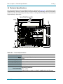
14 Technical Specifications . . . . . . . . . . . . . . . . . . . . . . . . . . . . . . . . . . . . . . . . . . . . . . . . . . . . . . . . 52
15 Hints for Handling the phyCORE-LPC3250 . . . . . . . . . . . . . . . . . . . . . . . . . . . . . . . . . . . . . . . . . 54
16 Component Placement Diagrams . . . . . . . . . . . . . . . . . . . . . . . . . . . . . . . . . . . . . . . . . . . . . . . . . 55
© PHYTEC America LLC 2009
i
Table of Contents
L-714e_1
Part II: PCM-967/phyCORE-LPC3250 Carrier Board. . . . . . . . . . . . . . . . . . . . . . . . . . . . . . . . . . . . . . . 57
17 Introduction . . . . . . . . . . . . . . . . . . . . . . . . . . . . . . . . . . . . . . . . . . . . . . . . . . . . . . . . . . . . . . . . . . 58
18 Overview of Peripherals . . . . . . . . . . . . . . . . . . . . . . . . . . . . . . . . . . . . . . . . . . . . . . . . . . . . . . . . 59
19 Jumpers . . . . . . . . . . . . . . . . . . . . . . . . . . . . . . . . . . . . . . . . . . . . . . . . . . . . . . . . . . . . . . . . . . . . 61
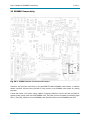
20 phyCORE-LPC3250 SOM Connectivity . . . . . . . . . . . . . . . . . . . . . . . . . . . . . . . . . . . . . . . . . . . . 65
21 Power . . . . . . . . . . . . . . . . . . . . . . . . . . . . . . . . . . . . . . . . . . . . . . . . . . . . . . . . . . . . . . . . . . . . . . 66
21.1 Wall Adapter Input . . . . . . . . . . . . . . . . . . . . . . . . . . . . . . . . . . . . . . . . . . . . . . . . . . . . . . . . 68
21.2 Power over Ethernet (PoE) . . . . . . . . . . . . . . . . . . . . . . . . . . . . . . . . . . . . . . . . . . . . . . . . . 69
21.3 Lithium-Ion Battery . . . . . . . . . . . . . . . . . . . . . . . . . . . . . . . . . . . . . . . . . . . . . . . . . . . . . . . 69
21.3.1 Battery Charging Circuit . . . . . . . . . . . . . . . . . . . . . . . . . . . . . . . . . . . . . . . . . . . 70
21.4 3.15V Supply (U9) . . . . . . . . . . . . . . . . . . . . . . . . . . . . . . . . . . . . . . . . . . . . . . . . . . . . . . . . 70
21.5 1.8V Supply (U10) . . . . . . . . . . . . . . . . . . . . . . . . . . . . . . . . . . . . . . . . . . . . . . . . . . . . . . . . 71
21.6 5.0V Buck-Boost Supply (U21) . . . . . . . . . . . . . . . . . . . . . . . . . . . . . . . . . . . . . . . . . . . . . . 71
21.7 Power Path Controller . . . . . . . . . . . . . . . . . . . . . . . . . . . . . . . . . . . . . . . . . . . . . . . . . . . . . 71
21.8 Current Measurement . . . . . . . . . . . . . . . . . . . . . . . . . . . . . . . . . . . . . . . . . . . . . . . . . . . . . 71
22 JTAG Connectivity . . . . . . . . . . . . . . . . . . . . . . . . . . . . . . . . . . . . . . . . . . . . . . . . . . . . . . . . . . . . 72
23 Deep Sleep Circuit . . . . . . . . . . . . . . . . . . . . . . . . . . . . . . . . . . . . . . . . . . . . . . . . . . . . . . . . . . . . 75
23.1 3.0V Deep Sleep Supply (U11) . . . . . . . . . . . . . . . . . . . . . . . . . . . . . . . . . . . . . . . . . . . . . . 79
24 Audio Interface . . . . . . . . . . . . . . . . . . . . . . . . . . . . . . . . . . . . . . . . . . . . . . . . . . . . . . . . . . . . . . . 80
25 Ethernet Connectivity . . . . . . . . . . . . . . . . . . . . . . . . . . . . . . . . . . . . . . . . . . . . . . . . . . . . . . . . . . 82
26 USB Connectivity . . . . . . . . . . . . . . . . . . . . . . . . . . . . . . . . . . . . . . . . . . . . . . . . . . . . . . . . . . . . . 84
27 LCD Connectivity . . . . . . . . . . . . . . . . . . . . . . . . . . . . . . . . . . . . . . . . . . . . . . . . . . . . . . . . . . . . . 86
28 GPIO Expansion Connector . . . . . . . . . . . . . . . . . . . . . . . . . . . . . . . . . . . . . . . . . . . . . . . . . . . . . 91
29 RS-232 Connectivity . . . . . . . . . . . . . . . . . . . . . . . . . . . . . . . . . . . . . . . . . . . . . . . . . . . . . . . . . . . 92
30 SD/MMC Connectivity . . . . . . . . . . . . . . . . . . . . . . . . . . . . . . . . . . . . . . . . . . . . . . . . . . . . . . . . . . 97
31 SDIO Connectivity. . . . . . . . . . . . . . . . . . . . . . . . . . . . . . . . . . . . . . . . . . . . . . . . . . . . . . . . . . . . . 99
32 Keyboard Connectivity . . . . . . . . . . . . . . . . . . . . . . . . . . . . . . . . . . . . . . . . . . . . . . . . . . . . . . . . 102
33 User Buttons . . . . . . . . . . . . . . . . . . . . . . . . . . . . . . . . . . . . . . . . . . . . . . . . . . . . . . . . . . . . . . . . 105
34 User LEDs. . . . . . . . . . . . . . . . . . . . . . . . . . . . . . . . . . . . . . . . . . . . . . . . . . . . . . . . . . . . . . . . . . 107
35 User ADC Potentiometer. . . . . . . . . . . . . . . . . . . . . . . . . . . . . . . . . . . . . . . . . . . . . . . . . . . . . . . 109
36 Boot Mode Selection . . . . . . . . . . . . . . . . . . . . . . . . . . . . . . . . . . . . . . . . . . . . . . . . . . . . . . . . . . 110
37 System Reset Button . . . . . . . . . . . . . . . . . . . . . . . . . . . . . . . . . . . . . . . . . . . . . . . . . . . . . . . . . 111
38 Watchdog Circuit. . . . . . . . . . . . . . . . . . . . . . . . . . . . . . . . . . . . . . . . . . . . . . . . . . . . . . . . . . . . . 112
Part III: PCM-988/GPIO Expansion Board . . . . . . . . . . . . . . . . . . . . . . . . . . . . . . . . . . . . . . . . . . . . . .
39 Introduction . . . . . . . . . . . . . . . . . . . . . . . . . . . . . . . . . . . . . . . . . . . . . . . . . . . . . . . . . . . . . . . . .
40 System Signal Mapping . . . . . . . . . . . . . . . . . . . . . . . . . . . . . . . . . . . . . . . . . . . . . . . . . . . . . . .
41 Memory Bus Signal Mapping . . . . . . . . . . . . . . . . . . . . . . . . . . . . . . . . . . . . . . . . . . . . . . . . . . .
42 LCD Signal Mapping . . . . . . . . . . . . . . . . . . . . . . . . . . . . . . . . . . . . . . . . . . . . . . . . . . . . . . . . . .
43 UART Signal Mapping. . . . . . . . . . . . . . . . . . . . . . . . . . . . . . . . . . . . . . . . . . . . . . . . . . . . . . . . .
44 I²C Signal Mapping . . . . . . . . . . . . . . . . . . . . . . . . . . . . . . . . . . . . . . . . . . . . . . . . . . . . . . . . . . .
45 GPIO Signal Mapping . . . . . . . . . . . . . . . . . . . . . . . . . . . . . . . . . . . . . . . . . . . . . . . . . . . . . . . . .
46 USB Signal Mapping . . . . . . . . . . . . . . . . . . . . . . . . . . . . . . . . . . . . . . . . . . . . . . . . . . . . . . . . . .
47 SSP Signal Mapping . . . . . . . . . . . . . . . . . . . . . . . . . . . . . . . . . . . . . . . . . . . . . . . . . . . . . . . . . .
48 I²S Signal Mapping . . . . . . . . . . . . . . . . . . . . . . . . . . . . . . . . . . . . . . . . . . . . . . . . . . . . . . . . . . .
49 Power Signal Mapping . . . . . . . . . . . . . . . . . . . . . . . . . . . . . . . . . . . . . . . . . . . . . . . . . . . . . . . .
113
114
116
117
119
120
121
122
123
124
125
126
Revision History . . . . . . . . . . . . . . . . . . . . . . . . . . . . . . . . . . . . . . . . . . . . . . . . . . . . . . . . . . . . . . . . . . 127
Index . . . . . . . . . . . . . . . . . . . . . . . . . . . . . . . . . . . . . . . . . . . . . . . . . . . . . . . . . . . . . . . . . . . . . . . . . . . . 128
© PHYTEC America LLC 2009
ii
List of Tables
L-714e_1
List of Tables
Conventions, Abbreviations and Acronyms . . . . . . . . . . . . . . . . . . . . . . . . . . . . . . . . . . . . . . . . . . . . .vi
Table 1-1. Abbreviations and Acronyms used in this Manual. . . . . . . . . . . . . . . . . . . . . . . . . . . . . vi
Part I: PCM-040/phyCORE-LPC3250 System on Module . . . . . . . . . . . . . . . . . . . . . . . . . . . . . . . . . . . . 1
Table 2-1. Pin Descriptions, phyCORE-Connector X2, Row A . . . . . . . . . . . . . . . . . . . . . . . . . . . 8
Table 2-2. Pin Descriptions, phyCORE-Connector X2, Row B . . . . . . . . . . . . . . . . . . . . . . . . . . 10
Table 2-3. Pin Descriptions, phyCORE-Connector X2, Row C . . . . . . . . . . . . . . . . . . . . . . . . . . 12
Table 2-4. Pin Descriptions, phyCORE-Connector X2, Row D . . . . . . . . . . . . . . . . . . . . . . . . . . 15
Table 3-1. Jumper Settings . . . . . . . . . . . . . . . . . . . . . . . . . . . . . . . . . . . . . . . . . . . . . . . . . . . . . 20
Table 4-1. U23 1.2V/1.8V Primary Voltage Regulator Jumper Settings . . . . . . . . . . . . . . . . . . . . 26
Table 4-2. U22 RTC/SDRAM Voltage Regulator Jumper Settings. . . . . . . . . . . . . . . . . . . . . . . . 27
Table 4-3. Primary System Supervisor Reset Thresholds . . . . . . . . . . . . . . . . . . . . . . . . . . . . . . 28
Table 4-4. Sleep System Supervisor Reset Thresholds . . . . . . . . . . . . . . . . . . . . . . . . . . . . . . . . 28
Table 9-1. Valid SDRAM Memory Address Ranges . . . . . . . . . . . . . . . . . . . . . . . . . . . . . . . . . . . 39
Table 9-2. NAND Flash Write Protection via Jumper J5 . . . . . . . . . . . . . . . . . . . . . . . . . . . . . . . 39
Table 9-3. Valid NOR Flash Memory Address Ranges . . . . . . . . . . . . . . . . . . . . . . . . . . . . . . . . 40
Table 9-4. EEPROM Configuration Struct dramcfg Field Format . . . . . . . . . . . . . . . . . . . . . . . . . 41
Table 9-5. EEPROM Configuration Struct syscfg Field Format . . . . . . . . . . . . . . . . . . . . . . . . . . 41
Table 9-6. phyCORE-LPC3250 Memory Map . . . . . . . . . . . . . . . . . . . . . . . . . . . . . . . . . . . . . . . 42
Table 10-1. UART 1/UART 5 TTL and RS-232 Level Signals . . . . . . . . . . . . . . . . . . . . . . . . . . . 43
Table 10-2. Ethernet PHY Operating Mode Selection . . . . . . . . . . . . . . . . . . . . . . . . . . . . . . . . . 45
Table 10-3. Applicable USB Operating Mode Connectors . . . . . . . . . . . . . . . . . . . . . . . . . . . . . . 46
Table 11-1. SDIO Controller to LPC3250 Signal Mapping . . . . . . . . . . . . . . . . . . . . . . . . . . . . . . 47
Table 11-2. SDIO Controller Interface Signals . . . . . . . . . . . . . . . . . . . . . . . . . . . . . . . . . . . . . . . 48
Table 13-1. Buffered Memory Bus Signal Mapping . . . . . . . . . . . . . . . . . . . . . . . . . . . . . . . . . . . 50
Table 13-2. Buffered Memory Bus Map . . . . . . . . . . . . . . . . . . . . . . . . . . . . . . . . . . . . . . . . . . . . 50
Table 14-1. Technical Specifications . . . . . . . . . . . . . . . . . . . . . . . . . . . . . . . . . . . . . . . . . . . . . . 52
Table 14-2. Static Operating Characteristics . . . . . . . . . . . . . . . . . . . . . . . . . . . . . . . . . . . . . . . . 53
Part II: PCM-967/phyCORE-LPC3250 Carrier Board. . . . . . . . . . . . . . . . . . . . . . . . . . . . . . . . . . . . . . . 57
Table 18-1. Connectors and Headers . . . . . . . . . . . . . . . . . . . . . . . . . . . . . . . . . . . . . . . . . . . . . 59
Table 18-2. Description of the Buttons and Switches . . . . . . . . . . . . . . . . . . . . . . . . . . . . . . . . . . 60
Table 18-3. Description of LEDs. . . . . . . . . . . . . . . . . . . . . . . . . . . . . . . . . . . . . . . . . . . . . . . . . . 60
Table 18-4. Description of Potentiometers . . . . . . . . . . . . . . . . . . . . . . . . . . . . . . . . . . . . . . . . . . 60
Table 19-1. Jumper Settings . . . . . . . . . . . . . . . . . . . . . . . . . . . . . . . . . . . . . . . . . . . . . . . . . . . . 62
Table 21-1. Possible Ethernet PSE Options. . . . . . . . . . . . . . . . . . . . . . . . . . . . . . . . . . . . . . . . . 69
Table 22-1. LPC3250 JTAG Connector X12 Pin Descriptions . . . . . . . . . . . . . . . . . . . . . . . . . . . 72
Table 22-2. Compatible JTAG Probes for the phyCORE-LPC3250 Carrier Board . . . . . . . . . . . 73
Table 27-1. LPC3250 LCD Port to Buffered CPLD Signal Mapping. . . . . . . . . . . . . . . . . . . . . . . 89
Table 27-2. LCD Mode Jumper Summary (JP48, JP49, JP50) . . . . . . . . . . . . . . . . . . . . . . . . . . 90
Table 29-1. Connector P1A (UART5) Pin Descriptions . . . . . . . . . . . . . . . . . . . . . . . . . . . . . . . . 93
Table 29-2. Connector P1B (UART3 and UART2) Pin Descriptions . . . . . . . . . . . . . . . . . . . . . . 93
Table 29-3. UART3/UART2 Header Connector X13 Pin Descriptions . . . . . . . . . . . . . . . . . . . . . 94
Table 29-4. Configuring DB-9 Connector P1B for UART3 or UART2 Operation . . . . . . . . . . . . . 95
Table 31-1. SDIO Easy Access Header Connector X23 Signal Descriptions . . . . . . . . . . . . . . 100
Table 32-1. Dip Switch S5 Positions and Associated Signals . . . . . . . . . . . . . . . . . . . . . . . . . . 103
Table 32-2. Dip Switch S6 Positions and Associated Signals . . . . . . . . . . . . . . . . . . . . . . . . . . 103
Table 32-3. Ethernet/Keyboard Easy Access Header Connector X11 Signal Descriptions . . . . 103
Part III: PCM-988/GPIO Expansion Board . . . . . . . . . . . . . . . . . . . . . . . . . . . . . . . . . . . . . . . . . . . . . . 113
Table 39-1. Signals Removed from the GPIO Expansion Connector. . . . . . . . . . . . . . . . . . . . . 115
© PHYTEC America LLC 2009
iii
List of Tables
L-714e_1
Table 40-1. System Signal Mapping. . . . . . . . . . . . . . . . . . . . . . . . . . . . . . . . . . . . . . . . . . . . . .
Table 41-1. Memory Bus Signal Mapping . . . . . . . . . . . . . . . . . . . . . . . . . . . . . . . . . . . . . . . . .
Table 42-1. LCD Signal Mapping . . . . . . . . . . . . . . . . . . . . . . . . . . . . . . . . . . . . . . . . . . . . . . . .
Table 43-1. UART Signal Mapping . . . . . . . . . . . . . . . . . . . . . . . . . . . . . . . . . . . . . . . . . . . . . . .
Table 44-1. I²C Signal Mapping . . . . . . . . . . . . . . . . . . . . . . . . . . . . . . . . . . . . . . . . . . . . . . . . .
Table 45-1. GPIO Signal Mapping . . . . . . . . . . . . . . . . . . . . . . . . . . . . . . . . . . . . . . . . . . . . . . .
Table 46-1. USB Signal Mapping . . . . . . . . . . . . . . . . . . . . . . . . . . . . . . . . . . . . . . . . . . . . . . . .
Table 47-1. SSP Signal Mapping . . . . . . . . . . . . . . . . . . . . . . . . . . . . . . . . . . . . . . . . . . . . . . . .
Table 48-1. I²S Signal Mapping . . . . . . . . . . . . . . . . . . . . . . . . . . . . . . . . . . . . . . . . . . . . . . . . .
Table 49-1. Power Signal Mapping . . . . . . . . . . . . . . . . . . . . . . . . . . . . . . . . . . . . . . . . . . . . . .
116
117
119
120
121
122
123
124
125
126
Revision History . . . . . . . . . . . . . . . . . . . . . . . . . . . . . . . . . . . . . . . . . . . . . . . . . . . . . . . . . . . . . . . . . . 127
Table 50-1. Revision History . . . . . . . . . . . . . . . . . . . . . . . . . . . . . . . . . . . . . . . . . . . . . . . . . . . 127
© PHYTEC America LLC 2009
iv
List of Figures
L-714e_1
List of Figures
Part I: PCM-040/phyCORE-LPC3250 System on Module . . . . . . . . . . . . . . . . . . . . . . . . . . . . . . . . . . . . 1
Fig. 1-1. phyCORE-LPC3250 Block Diagram. . . . . . . . . . . . . . . . . . . . . . . . . . . . . . . . . . . . . . . . . 4
Fig. 1-2. Top View of the phyCORE-LPC3250 (Controller Side) . . . . . . . . . . . . . . . . . . . . . . . . . . 5
Fig. 1-3. Bottom View of the phyCORE-LPC3250 (Connector Side) . . . . . . . . . . . . . . . . . . . . . . . 6
Fig. 2-1. Pin-out of the phyCORE-Connector (Top View, with Cross Section Insert) . . . . . . . . . . . 8
Fig. 3-1. Jumper Locations (Controller Side) . . . . . . . . . . . . . . . . . . . . . . . . . . . . . . . . . . . . . . . . 19
Fig. 3-2. Jumper Locations (Connector Side) . . . . . . . . . . . . . . . . . . . . . . . . . . . . . . . . . . . . . . . . 20
Fig. 3-3. Default Jumper Settings (Controller Side) . . . . . . . . . . . . . . . . . . . . . . . . . . . . . . . . . . . 22
Fig. 3-4. Default Jumper Settings (Connector Side) . . . . . . . . . . . . . . . . . . . . . . . . . . . . . . . . . . . 23
Fig. 4-1. phyCORE-LPC3250 On-board Powering Scheme. . . . . . . . . . . . . . . . . . . . . . . . . . . . . 26
Fig. 5-1. Typical phyCORE-LPC3250 Sleep Enabled Powering Scheme . . . . . . . . . . . . . . . . . . 30
Fig. 8-1. Small Page SLC NAND Flash Structure . . . . . . . . . . . . . . . . . . . . . . . . . . . . . . . . . . . . 36
Fig. 10-1. Ethernet PHY Disconnection Resistors . . . . . . . . . . . . . . . . . . . . . . . . . . . . . . . . . . . . 44
Fig. 12-1. JTAG Interface X1 (Controller Side). . . . . . . . . . . . . . . . . . . . . . . . . . . . . . . . . . . . . . . 49
Fig. 14-1. phyCORE-LPC3250 Physical Dimensions . . . . . . . . . . . . . . . . . . . . . . . . . . . . . . . . . . 52
Fig. 16-1. phyCORE-LPC3250 Component Placement (Controller Side) . . . . . . . . . . . . . . . . . . 55
Fig. 16-2. phyCORE-LPC3250 Component Placement (Connector Side) . . . . . . . . . . . . . . . . . . 56
Part II: PCM-967/phyCORE-LPC3250 Carrier Board. . . . . . . . . . . . . . . . . . . . . . . . . . . . . . . . . . . . . . . 57
Fig. 17-1. phyCORE-LPC3250 Carrier Board Overview of Connectors and Interfaces . . . . . . . . 58
Fig. 19-1. Jumper Locations and Default Settings . . . . . . . . . . . . . . . . . . . . . . . . . . . . . . . . . . . . 61
Fig. 19-2. Typical Jumper Pad Numbering Scheme (Removable Jumpers) . . . . . . . . . . . . . . . . 62
Fig. 20-1. phyCORE-LPC3250 SOM Connectivity to the Carrier Board. . . . . . . . . . . . . . . . . . . . 65
Fig. 21-1. Powering Scheme . . . . . . . . . . . . . . . . . . . . . . . . . . . . . . . . . . . . . . . . . . . . . . . . . . . . 66
Fig. 21-2. Powering Scheme Block Diagram . . . . . . . . . . . . . . . . . . . . . . . . . . . . . . . . . . . . . . . . 68
Fig. 22-1. JTAG Probe Connectivity to the LPC3250 . . . . . . . . . . . . . . . . . . . . . . . . . . . . . . . . . . 72
Fig. 23-1. Deep Sleep Jumpers and Power Button . . . . . . . . . . . . . . . . . . . . . . . . . . . . . . . . . . . 75
Fig. 23-2. Deep Sleep Circuit Block Diagram . . . . . . . . . . . . . . . . . . . . . . . . . . . . . . . . . . . . . . . . 76
Fig. 23-3. Deep Sleep State Diagram. . . . . . . . . . . . . . . . . . . . . . . . . . . . . . . . . . . . . . . . . . . . . . 78
Fig. 24-1. Audio Interface Connectors and Jumpers . . . . . . . . . . . . . . . . . . . . . . . . . . . . . . . . . . 80
Fig. 25-1. Ethernet Interface Connectors and Jumpers . . . . . . . . . . . . . . . . . . . . . . . . . . . . . . . . 82
Fig. 26-1. USB Interface Connectors and Jumpers . . . . . . . . . . . . . . . . . . . . . . . . . . . . . . . . . . . 84
Fig. 27-1. LCD Interface Connectors and Jumpers . . . . . . . . . . . . . . . . . . . . . . . . . . . . . . . . . . . 86
Fig. 27-2. LCD BLUE Signal Mapping in 24-bit Mode with a 24-Bit LCD . . . . . . . . . . . . . . . . . . . 87
Fig. 27-3. LCD BLUE Signal Mapping in 16-bit Mode with an 18-Bit LCD . . . . . . . . . . . . . . . . . . 87
Fig. 28-1. GPIO Expansion Connector . . . . . . . . . . . . . . . . . . . . . . . . . . . . . . . . . . . . . . . . . . . . . 91
Fig. 29-1. RS-232 Interface Connectors and Jumpers . . . . . . . . . . . . . . . . . . . . . . . . . . . . . . . . . 92
Fig. 29-2. DB-9 RS-232 Connectors P1A and P1B Pin Numbering . . . . . . . . . . . . . . . . . . . . . . . 93
Fig. 29-3. UART3/UART2 Header Connector X13 Pin Numbering . . . . . . . . . . . . . . . . . . . . . . . 94
Fig. 30-1. SD/MMC Interface Connectors and Jumpers. . . . . . . . . . . . . . . . . . . . . . . . . . . . . . . . 97
Fig. 31-1. SDIO Interface Connectors and Jumpers . . . . . . . . . . . . . . . . . . . . . . . . . . . . . . . . . . 99
Fig. 32-1. Keyboard Interface Connector and Dip Switches. . . . . . . . . . . . . . . . . . . . . . . . . . . . 102
Fig. 33-1. User Buttons and Jumpers . . . . . . . . . . . . . . . . . . . . . . . . . . . . . . . . . . . . . . . . . . . . . 105
Fig. 34-1. User LEDs and Jumpers . . . . . . . . . . . . . . . . . . . . . . . . . . . . . . . . . . . . . . . . . . . . . . 107
Fig. 35-1. User ADC Potentiometer and Jumper . . . . . . . . . . . . . . . . . . . . . . . . . . . . . . . . . . . . 109
Fig. 36-1. Boot Mode Selection Jumper . . . . . . . . . . . . . . . . . . . . . . . . . . . . . . . . . . . . . . . . . . . 110
Fig. 37-1. System Reset Button . . . . . . . . . . . . . . . . . . . . . . . . . . . . . . . . . . . . . . . . . . . . . . . . . 111
Fig. 38-1. Watchdog Enable Jumper . . . . . . . . . . . . . . . . . . . . . . . . . . . . . . . . . . . . . . . . . . . . . 112
Part III: PCM-988/GPIO Expansion Board . . . . . . . . . . . . . . . . . . . . . . . . . . . . . . . . . . . . . . . . . . . . . . 113
Fig. 39-1. PCM-988/GPIO Expansion Board and Patch Field . . . . . . . . . . . . . . . . . . . . . . . . . . 114
© PHYTEC America LLC 2009
v
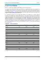
Conventions, Abbreviations and Acronyms
L-714e_1
Conventions, Abbreviations and Acronyms
Conventions
The conventions used in this manual are as follows:
• Signals that are preceded by a “/” character are designated as active low signals. That is, their
active state is when they are driven low, or are driving low; e.g., /RESET.
• Tables which describe jumper settings show the default position in bold, teal text.
• Text in blue indicates a hyperlink within, or external to the document. Click these links to quickly
jump to the applicable URL, part, chapter, table, or figure.
• References made to the phyCORE-Connector always refer to the high density molex connectors
on the underside of the phyCORE-LPC3250 System on Module.
Abbreviations and Acronyms
Many acronyms and abbreviations are used throughout this manual. Use the table below to navigate
unfamiliar terms used in this document.
Table 1-1. Abbreviations and Acronyms used in this Manual
Abbreviation Definition
GPIO
General purpose input and output.
GPI
General purpose input.
GPO
General purpose output.
BTN1
User button 1; used in reference to one of the two available user buttons on the Carrier
Board.
BTN2
User button 2; used in reference to one of the two available user buttons on the Carrier
Board.
CB
Carrier Board; used in reference to the PCM-967/phyCORE-LPC3250 Carrier Board.
DFF
D flip-flop.
EMB
External memory bus.
EMI
Electromagnetic Interference.
GPIOEBPF
GPIO Expansion Board Patch Field; used in reference with the PCM-988/GPIO Expansion Board and its associated patch field.
IRAM
Internal RAM; the internal static RAM on the LPC3250 processor.
J
Solder jumper; these types of jumpers require solder equipment to remove and place.
JP
Solderless jumper; these types of jumpers can be removed and placed by hand with no
special tools.
KS
Kickstart; the second level bootloader flashed on the phyCORE-LPC3250 SOM.
PCB
Printed circuit board.
PoE
Power-over-Ethernet.
POT
Potentiometer.
PSE
Power sourcing equipment; the device in a PoE network that provides power to connected devices--usually a switch, router, or stand alone power injector.
RTC
Real-time clock.
S1L
Stage 1 Loader; the third level bootloader flashed on the phyCORE-LPC3250 SOM.
SMT
Surface mount technology.
© PHYTEC America LLC 2009
vi
Conventions, Abbreviations and Acronyms
L-714e_1
Table 1-1. Abbreviations and Acronyms used in this Manual (Continued)
Abbreviation Definition
SOM
System on Module; used in reference to the PCM-040/phyCORE-LPC3250 System on
Module.
VBAT
SOM battery supply input
VFP
Vector floating point.
© PHYTEC America LLC 2009
vii
L-714e_1
Preface
This phyCORE-ARM9/LPC3250 Hardware Manual describes the single board computer's design and
functions. Precise specifications for the NXP Semiconductors LPC3250 processor can be found in the
enclosed processor Data Sheet/User's Manual. If software is included please also refer to additional
documentation for this software.
In this hardware manual and in the attached schematics, low active signals are denoted by a "/" preceding
the signal name (i.e.: /RD). A "0" indicates a logic-zero or low-level signal, while a "1" represents a logicone or high-level signal.
Declaration of Electro Magnetic Conformity of the PHYTEC
phyCORE-LPC3250
PHYTEC System on Modules (SOMs) are designed for installation in electrical appliances or, combined
with the PHYTEC Carrier Board, can be used as dedicated Evaluation Boards (i.e.: for use as a test and
prototype platform for hardware/software development) in laboratory environments.
CAUTION:
PHYTEC products lacking protective enclosures are subject to damage by ESD and, hence, may only be
unpacked, handled or operated in environments in which sufficient precautionary measures have been
taken in respect to ESD-dangers. It is also necessary that only appropriately trained personnel (such as
electricians, technicians and engineers) handle and/or operate these products. Moreover, PHYTEC
products should not be operated without protection circuitry if connections to the product's pin header
rows are longer than 3 m.
PHYTEC products fulfill the norms of the European Union's Directive for Electro Magnetic Conformity only
in accordance to the descriptions and rules of usage indicated in this hardware manual (particularly in
respect to the pin header row connectors, power connector and serial interface to a host-PC).
Implementation of PHYTEC products into target devices, as well as user modifications and extensions of
PHYTEC products, is subject to renewed establishment of conformity to, and certification of, Electro
Magnetic Directives. Users should ensure conformance following any modifications to the products as
well as implementation of the products into target systems.
The phyCORE-LPC3250 is one of a series of PHYTEC System on Modules that can be populated with
different controllers and, hence, offers various functions and configurations. PHYTEC supports a variety of
8-/16- and 32-bit controllers in two ways:
1. As the basis for Rapid Development Kits which serve as a reference and evaluation platform.
2. As insert-ready, fully functional phyCORE OEM modules, which can be embedded directly into the
user's peripheral hardware, design.
Implementation of an OEM-able SOM subassembly as the "core" of your embedded design allows you to
focus on hardware peripherals and firmware without expending resources to "re-invent" microcontroller
circuitry. Furthermore, much of the value of the phyCORE module lies in its layout and test.
Production-ready Board Support Packages (BSPs) and Design Services for our hardware further reduce
development time and expenses. Take advantage of PHYTEC products to shorten time-to-market, reduce
development costs, and avoid substantial design issues and risks. For more information go to:
http://www.phytec.com/services/phytec-advantage.html
© PHYTEC America LLC 2009
viii
PCM-040/phyCORE-LPC3250 System on Module
L-714e_1
Part I: PCM-040/phyCORE-LPC3250 System on
Module
Part 1 of this 3 part manual provides detailed information on the phyCORE-ARM9/LPC3250 System on
Module (SOM) designed for custom integration into customer applications.
The information in the following chapters is applicable to the 1304.1 PCB revision of the phyCORELPC3250 SOM.
© PHYTEC America LLC 2009
1
Part I, Chapter 1: Introduction
L-714e_1
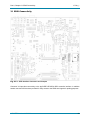
1 Introduction
The phyCORE-LPC3250 belongs to PHYTEC’s phyCORE System on Module (SOM) family. The
phyCORE SOMs represent the continuous development of PHYTEC SOM technology. Like its mini-,
micro- and nanoMODUL predecessors, the phyCORE boards integrate all core elements of a
microcontroller system on a subminiature board and are designed in a manner that ensures their easy
expansion and embedding in peripheral hardware developments.
As independent research indicates that approximately 70% of all EMI (Electro Magnetic Interference)
problems stem from insufficient supply voltage grounding of electronic components in high frequency
environments, the phyCORE board design features an increased pin package. The increased pin package
allows dedication of approximately 20% of all connector pins on the phyCORE boards to ground. This
improves EMI and EMC characteristics and makes it easier to design complex applications meeting EMI
and EMC guidelines using phyCORE boards even in high noise environments.
phyCORE boards achieve their small size through modern SMD technology and multi-layer design. In
accordance with the complexity of the module, 0402-packaged SMD components and laser-drilled
Microvias are used on the boards, providing phyCORE users with access to this cutting edge
miniaturization technology for integration into their own design.
The phyCORE-LPC3250 is a sub-miniature (70 x 58 mm) insert-ready SOM populated with the NXP
LPC3250 ARM926EJ-S core processor. Its universal design enables its insertion in a wide range of
embedded applications. All processor signals and ports extend from the processor to high-density pitch
(0.635 mm) connectors aligning two sides of the board, allowing it to be plugged like a "big chip" into a
target application.
Precise specifications for the processor populating the board can be found in the applicable processor
User’s Manual or datasheet. The descriptions in this manual are based on the NXP Semiconductors
ARM9/LPC3250 processor. No description of compatible processor derivative functions is included, as
such functions are not relevant for the basic functioning of the phyCORE-LPC3250.
The phyCORE-LPC3250 offers the following features:
• Insert-ready, sub-miniature (70 x 58 mm) System on Module (SOM) subassembly in low EMI
design, achieved through advanced SMD technology
• Populated with the NXP LPC3250 processor (296-ball BGA packaging)
• Improved interference safety achieved through multi-layer PCB technology and dedicated ground
pins
• Controller signals and ports extend to two 160-pin high-density (0.635 mm) Molex connectors
aligning two sides of the board, enabling it to be plugged like a "big chip" into target application
• Max. 208 MHz core clock frequency
• Vector Floating Point coprocessor supporting single-precision and double-precision add, subtract,
multiply, divide, and multiply-accumulate at CPU clock speeds.
• Memory Management Unit (MMU), Memory and DMA controllers
• 64 MB of external address space, with bus buffers to condition and protect signal load of
peripherals on the LPC3250 external memory bus
• 1 to 8 MB of on-board NOR Flash operating at 1.8V or 3.15V
• 16 to 128 MB of on-board NAND flash at 1.8V
• 16 to 128MB of on-board 1.8V mobile SDRAM at 104 MHz
• 32 KByte SPI bootable EEPROM
• USB OTG transceiver for embedded USB host/peripheral functionality
• 6 rail voltage supervision with deep sleep supervision support
• On-board high efficiency switching regulators generating 1.8, 1.2, and an adjustable 0.9-1.2
voltage supplies
• Processor independent watchdog with disable, normal, and extended modes
© PHYTEC America LLC 2009
2
Part I, Chapter 1: Introduction
•
•
•
•
•
•
•
•
•
•
•
•
•
•
•
•
•
•
•
•
•
•
L-714e_1
Support for ETM9 and Embedded ICE-RT debug through JTAG interface
Keyboard support for up to 64 keys in an 8 x 8 matrix (Ethernet must be disabled to support this
feature)
2x SPI ports
2x SSP ports
7x UARTs – 3 high speed (920kbps), 4 standard speed (460kbps), 1 supporting IrDA with 2x at
RS-232 levels
2x I²S ports
2x I²C ports
10/100 Ethernet with HP Auto MDIX support
24-bit LCD controller supporting STN and TFT panels at up to 1024x768 display resolution
Integrated LCD touch screen controller
SD/MMC card interface
SDIO controller
Internal controller based RTC with 32 byte scratch pad memory
External processor independent ultra low power RTC consuming 275nA @ 3.0V typical
32-bit high speed timer
4x timer/counters with capture inputs and match outputs
32-bit millisecond timer driven from the RTC clock
Processor based watchdog timer
12x PWM outputs
JTAG interface for debugging and download of user code
Single supply voltage of 3.15V with on-board power management
Industrial temperature range (-40°...+85°)
© PHYTEC America LLC 2009
3
Part I, Chapter 1: Introduction
L-714e_1
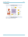
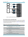
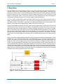
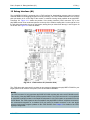
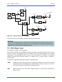
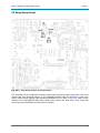
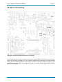
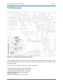
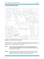
1.1 Block Diagram
Fig. 1-1. phyCORE-LPC3250 Block Diagram
© PHYTEC America LLC 2009
4
Part I, Chapter 1: Introduction
L-714e_1
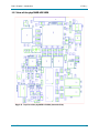
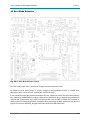
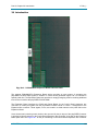
1.2 View of the phyCORE-LPC3250
Fig. 1-2. Top View of the phyCORE-LPC3250 (Controller Side)
© PHYTEC America LLC 2009
5
Part I, Chapter 1: Introduction
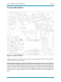
L-714e_1
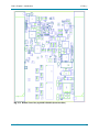
Fig. 1-3. Bottom View of the phyCORE-LPC3250 (Connector Side)
© PHYTEC America LLC 2009
6
Part I, Chapter 2: Pin Description
L-714e_1
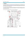
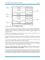
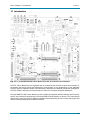
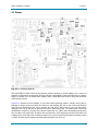
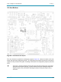
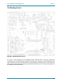
2 Pin Description
Please note that all module connections are not to exceed their expressed maximum voltage or current.
Maximum signal input values are indicated in the corresponding controller manuals/data sheets. As
damage from improper connections varies according to use and application, it is the user's responsibility to
take appropriate safety measures to ensure that the module connections are protected from overloading
through connected peripherals.
All controller signals extend to surface mount technology (SMT) connectors (0.635 mm) lining two sides of
the module (referred to as the phyCORE-Connector). This allows the phyCORE-LPC3250 to be plugged
into any target application like a "big chip".
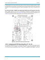
The numbering scheme for the phyCORE-Connector is based on a two dimensional matrix in which
column positions are identified by a letter and row position by a number. Pin 1A, for example, is always
located in the upper left hand corner of the matrix. The pin numbering values increase moving down on the
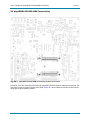
board. Lettering of the pin connector rows progresses alphabetically from left to right (refer to Figure 2-1).
The numbered matrix can be aligned with the phyCORE-LPC3250 (viewed from above; phyCOREConnector pointing down) or with the socket of the corresponding phyCORE Carrier Board/user target
circuitry. The upper left-hand corner of the numbered matrix (pin 1A) is thus covered with the corner of the
phyCORE-LPC3250 marked with a white triangle. The numbering scheme is always in relation to the PCB
as viewed from above, even if all connector contacts extend to the bottom of the module.
The numbering scheme is thus consistent for both the module’s phyCORE-Connector as well as mating
connectors on the phyCORE Carrier Board or target hardware, thereby considerably reducing the risk of
pin identification errors.
Since the pins are exactly defined according to the numbered matrix previously described, the phyCOREConnector is usually assigned a single designator for its position (X1 for example). In this manner the
phyCORE-Connector comprises a single, logical unit regardless of the fact that it could consist of more
than one physical socketed connector. The location of row 1 on the board is marked by a white triangle on
the PCB to allow easy identification.
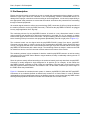
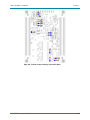
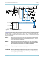
Figure 2-1 illustrates the numbered matrix system. It shows a phyCORE-LPC3250 with SMT phyCOREConnectors on its underside (defined as dotted lines) mounted on a Carrier Board. In order to facilitate
understanding of the pin assignment scheme, the diagram presents a cross-view of the phyCORE module
showing these phyCORE-Connectors mounted on the underside of the module’s PCB.
© PHYTEC America LLC 2009
7
Part I, Chapter 2: Pin Description
L-714e_1
Fig. 2-1. Pin-out of the phyCORE-Connector (Top View, with Cross
Section Insert)
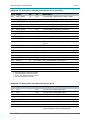
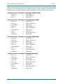
Table 2-1. Pin Descriptions, phyCORE-Connector X2, Row A
Pin #
Signal
I/O
SL
Description
1A
N/C
-
-
Not connected
2A
GND
-
-
Ground
3A
N/C
-
-
Not connected
4A
N/C
-
-
Not connected
5A
b_/CS0
O
VCC_EMB
Buffered µC signal /CS0 (memory bus chip select 0)
6A
b_/CS1
O
VCC_EMB
Buffered µC signal /CS1 (memory bus chip select 1)
7A
GND
-
-
8A
b_/WR
O
VCC_EMB
Buffered µC signal /WR (memory bus write enable)
9A
b_A1
O
VCC_EMB
Buffered µC signal A1 (memory bus address bit A1)
10A
b_A2
O
VCC_EMB
Buffered µC signal A2 (memory bus address bit A2)
11A
b_A4
O
VCC_EMB
Buffered µC signal A4 (memory bus address bit A4)
12A
GND
-
-
13A
b_A7
O
VCC_EMB
Buffered µC signal A7 (memory bus address bit A7)
14A
b_A9
O
VCC_EMB
Buffered µC signal A9 (memory bus address bit A9)
15A
b_A10
O
VCC_EMB
Buffered µC signal A10 (memory bus address bit A10)
16A
b_A12
O
VCC_EMB
Buffered µC signal A12 (memory bus address bit A12)
17A
GND
-
-
18A
b_A15
O
VCC_EMB
Buffered µC signal A15 (memory bus address bit A15)
19A
b_D1
I/O
VCC_EMB
Buffered µC signal D1 (memory bus data bit D1)
20A
b_D2
I/O
VCC_EMB
Buffered µC signal D2 (memory bus data bit D2)
21A
b_D4
I/O
VCC_EMB
Buffered µC signal D4 (memory bus data bit D4)
22A
GND
-
-
23A
b_D7
I/O
VCC_EMB
© PHYTEC America LLC 2009
Ground
Ground
Ground
Ground
Buffered µC signal D7 (memory bus data bit D7)
8
Part I, Chapter 2: Pin Description
L-714e_1
Table 2-1. Pin Descriptions, phyCORE-Connector X2, Row A (Continued)
Pin #
Signal
I/O
SL
24A
b_A17
O
VCC_EMB
Buffered µC signal A17 (memory bus address bit A17)
25A
b_A18
O
VCC_EMB
Buffered µC signal A18 (memory bus address bit A18)
26A
b_A20
O
VCC_EMB
Buffered µC signal A20 (memory bus address bit A20)
27A
GND
-
-
28A
b_A23
O
VCC_EMB
Buffered µC signal A23 (memory bus address bit A23)
29A
b_D9
I/O
VCC_EMB
Buffered µC signal D9 (memory bus data bit D9)
30A
b_D10
I/O
VCC_EMB
Buffered µC signal D10 (memory bus data bit D10)
31A
b_D12
I/O
VCC_EMB
Buffered µC signal D12 (memory bus data bit D12)
32A
GND
-
-
33A
b_D15
I/O
VCC_EMB
Buffered µC signal D15 (memory bus data bit D15)
34A
b_BLS0
O
VCC_EMB
Buffered µC signal BLS0 (memory bus byte lane select 0)
35A
b_BLS2
O
VCC_EMB
Buffered µC signal BLS2 (memory bus byte lane select 2)
36A
N/C
-
-
Not connected
37A
GND
-
-
Ground
38A
b_D17
I/O
VCC_EMB
Buffered µC signal D17 (memory bus data bit D17)
39A
b_D19
I/O
VCC_EMB
Buffered µC signal D19 (memory bus data bit D19)
40A
b_D20
I/O
VCC_EMB
Buffered µC signal D20 (memory bus data bit D20)
41A
b_D22
I/O
VCC_EMB
Buffered µC signal D22 (memory bus data bit D22)
42A
GND
-
-
43A
b_D25
I/O
VCC_EMB
Buffered µC signal D25 (memory bus data bit D25)
44A
b_D27
I/O
VCC_EMB
Buffered µC signal D27 (memory bus data bit D27)
45A
b_D28
I/O
VCC_EMB
Buffered µC signal D28 (memory bus data bit D28)
46A
b_D30
I/O
VCC_EMB
Buffered µC signal D30 (memory bus data bit D30)
47A
GND
-
-
48A
LCD21
O
VCC
µC signal LCD21 (blue color bit)
49A
LCD20
O
VCC
µC signal LCD20 (blue color bit)
50A
LCD19
O
VCC
µC signal LCD19 (blue color bit)
51A
LCD17
O
VCC
µC signal LCD17 (blue color bit)
52A
GND
-
-
53A
LCD14
O
VCC
µC signal LCD14 (green color bit)
54A
LCD13
O
VCC
µC signal LCD13 (green color bit)
55A
LCD11
O
VCC
µC signal LCD11 (green color bit)
56A
LCD10
O
VCC
µC signal LCD10 (green color bit)
57A
GND
-
-
58A
LCD7
O
VCC
µC signal LCD7 (red color bit)
59A
LCD4
O
VCC
µC signal LCD4 (red color bit)
60A
LCD3
O
VCC
µC signal LCD3 (red color bit)
61A
LDC0
O
VCC
µC signal LCD0 (red color bit)
© PHYTEC America LLC 2009
Description
Ground
Ground
Ground
Ground
Ground
Ground
9
Part I, Chapter 2: Pin Description
L-714e_1
Table 2-1. Pin Descriptions, phyCORE-Connector X2, Row A (Continued)
Pin #
Signal
I/O
SL
62A
Description
GND
-
-
63A
LCDFP
O
VCC
µC signal LCDFP (STN frame pulse/TFT vertical sync)
64A
LCDLP
O
VCC
µC signal LCDLP (STN line pulse/TFT horizontal sync)
65A
LCDCP
O
VCC
µC signal LCDCP (pixel clock)
66A
LCDLE
O
VCC
µC signal LCDLE (line end)
67A
GND
-
-
68A
MS_DIO0
I/O
VCC
µC signal MS_DIO0 (MMC/SD data I/O 0)
69A
MS_DIO2
I/O
VCC
µC signal MS_DIO2 (MMC/SD data I/O 2)
70A
MS_BS
I/O
VCC
µC signal MS_BS (MMC/SD command I/O)
71A
MS_SCLK
O
-
µC signal MS_SCLK (MMC/SD clock output)
72A
GND
-
-
Ground
73A
TMS
I
VCC
µC signal TMS (JTAG test mode select)
74A
TDI
I
VCC
µC signal TDI (JTAG test data input)
75A
/TRST
I
VCC
µC signal /TRST (JTAG test logic reset)
76A
N/C
-
-
Not connected
77A
GND
-
-
Ground
78A
N/C
-
-
Not connected
79A
N/C
-
-
Not connected
80A
N/C
-
-
Not connected
Ground
Ground
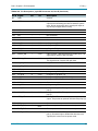
Table 2-2. Pin Descriptions, phyCORE-Connector X2, Row B
Pin # Signal
I/O
SL
Description
1B
N/C
-
-
Not connected
2B
N/C
-
-
Not connected
3B
N/C
-
-
Not connected
4B
GND
-
-
Ground
5B
b_/CS3
O
VCC_EMB Buffered µC signal /CS3 (memory bus chip select 3)
6B
b_/CS2
O
VCC_EMB Buffered µC signal /CS2 (memory bus chip select 2)
7B
b_/OE
O
VCC_EMB Buffered µC signal /OE (memory bus output enable)
8B
b_A0
O
VCC_EMB Buffered µC signal A0 (memory bus address bit A0)
9B
GND
-
10B
b_A3
O
VCC_EMB Buffered µC signal A3 (memory bus address bit 3)
11B
b_A5
O
VCC_EMB Buffered µC signal A5 (memory bus address bit A5)
12B
b_A6
O
VCC_EMB Buffered µC signal A6 (memory bus address bit A6)
13B
b_A8
O
VCC_EMB Buffered µC signal A8 (memory bus address bit A8)
14B
GND
-
15B
b_A11
O
-
-
Ground
Ground
VCC_EMB Buffered µC signal A11 (memory bus address bit A11)
© PHYTEC America LLC 2009
10
Part I, Chapter 2: Pin Description
L-714e_1
Table 2-2. Pin Descriptions, phyCORE-Connector X2, Row B (Continued)
Pin # Signal
I/O
SL
Description
16B
b_A13
O
VCC_EMB Buffered µC signal A13 (memory bus address bit A13)
17B
b_A14
O
VCC_EMB Buffered µC signal A14 (memory bus address bit A14)
18B
b_D0
I/O VCC_EMB Buffered µC signal D0 (memory bus data bit D0)
19B
GND
20B
b_D3
I/O VCC_EMB Buffered µC signal D3 (memory bus data bit D3)
21B
b_D5
I/O VCC_EMB Buffered µC signal D5 (memory bus data bit D5)
22B
b_D6
I/O VCC_EMB Buffered µC signal D6 (memory bus data bit D6)
23B
b_A16
O
24B
GND
-
25B
b_A19
O
VCC_EMB Buffered µC signal A19 (memory bus address bit A19)
26B
b_A21
O
VCC_EMB Buffered µC signal A21 (memory bus address bit A21)
27B
b_A22
O
VCC_EMB Buffered µC signal A22 (memory bus address bit A22)
28B
b_D8
I/O VCC_EMB Buffered µC signal D8 (memory bus data bit D8)
29B
GND
30B
b_D11
I/O VCC_EMB Buffered µC signal D11 (memory bus data bit D11)
31B
b_D13
I/O VCC_EMB Buffered µC signal D13 (memory bus data bit D13)
32B
b_D14
I/O VCC_EMB Buffered µC signal D14 (memory bus data bit D14)
33B
b_BLS1
O
34B
GND
-
35B
b_BLS3
O
36B
N/C
-
37B
b_D16
I/O VCC_EMB Buffered µC signal D16 (memory bus data bit D16)
38B
b_D18
I/O VCC_EMB Buffered µC signal D18 (memory bus data bit D18)
39B
GND
40B
b_D21
I/O VCC_EMB Buffered µC signal D21 (memory bus data bit D21)
41B
b_D23
I/O VCC_EMB Buffered µC signal D23 (memory bus data bit D23)
42B
b_D24
I/O VCC_EMB Buffered µC signal D24(memory bus data bit D24)
43B
b_D26
I/O VCC_EMB Buffered µC signal D26 (memory bus data bit D26)
44B
GND
45B
b_D29
I/O VCC_EMB Buffered µC signal D29 (memory bus data bit D29)
46B
b_D31
I/O VCC_EMB Buffered µC signal D31 (memory bus data bit D31)
47B
LCD23
O
VCC
µC signal LCD23 (blue color bit)
48B
LCD22
O
VCC
µC signal LCD22 (blue color bit)
49B
GND
-
-
50B
LCD18
O
VCC
µC signal LCD18 (blue color bit)
51B
LCD16
O
VCC
µC signal LCD16 (blue color bit)
52B
LCD15
O
VCC
µC signal LCD15 (green color bit)
53B
LCD12
O
VCC
µC signal LCD12 (green color bit)
-
-
Ground
VCC_EMB Buffered µC signal A16 (memory bus address bit A16)
-
-
-
Ground
Ground
VCC_EMB Buffered µC signal BLS1 (memory bus byte lane select 1)
-
Ground
VCC_EMB Buffered µC signal BLS3 (memory bus byte lane select 3)
-
-
-
-
-
© PHYTEC America LLC 2009
Not connected
Ground
Ground
Ground
11
Part I, Chapter 2: Pin Description
L-714e_1
Table 2-2. Pin Descriptions, phyCORE-Connector X2, Row B (Continued)
Pin # Signal
I/O
SL
Description
54B
GND
-
-
Ground
55B
LCD9
O
VCC
µC signal LCD9 (green color bit)
56B
LCD8
O
VCC
µC signal LCD8 (green color bit)
57B
LCD6
O
VCC
µC signal LCD6 (red color bit)
58B
LCD5
O
VCC
µC signal LCD5 (red color bit)
59B
GND
-
-
60B
LCD2
O
VCC
µC signal LCD2 (red color bit)
61B
LCD1
O
VCC
µC signal LCD1 (red color bit)
62B
LCDPWR
O
VCC
µC signal LCDPWR (panel power enable)
63B
LCDCLKIN
I
VCC
µC signal LCDCLKIN (optional clock input signal)
64B
GND
-
-
65B
LCDAC
O
VCC
µC signal LCDAC (STN AC bias/TFT data enable)
66B
MS_DIO1
I/O
VCC
µC signal MS_DIO1 (MMC/SD data I/O 1)
67B
MS_DIO3
I/O
VCC
µC signal MS_DIO3 (MMC/SD data I/O 3)
68B
N/C
-
-
Not connected
69B
GND
-
-
Ground
70B
TDO
O
VCC
µC signal TMS (JTAG test data output)
71B
TCK
I
VCC
µC signal TMS (JTAG test clock input); Internal 10k pull-down
72B
RTCK
O
VCC
µC signal TMS (JTAG test clock return output); Internal 10k pulldown
73B
DBGEN
I
VCC
µC signal DBGEN (JTAG/boundary scan select)
74B
GND
-
-
Ground
75B
N/C
-
-
Not connected
76B
N/C
-
-
Not connected
77B
N/C
-
-
Not connected
78B
N/C
-
-
Not connected
79B
GND
-
-
Ground
80B
N/C
-
-
Not connected
Ground
Ground
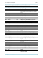
Table 2-3. Pin Descriptions, phyCORE-Connector X2, Row C
Pin # Signal
I/O
SL
Description
1C
VCC
I
3.15V
3.15V primary voltage supply input
2C
VCC
I
3.15V
3.15V primary voltage supply input
3C
GND
-
-
4C
VCC_SDIO
5C
VCC_SDIO
Ground
I
a
2.25 – 3.6V
SDIO controller voltage interface select
I
2.25 – 3.6Vb
SDIO controller voltage interface select
© PHYTEC America LLC 2009
12
Part I, Chapter 2: Pin Description
L-714e_1
Table 2-3. Pin Descriptions, phyCORE-Connector X2, Row C (Continued)
Pin # Signal
I/O
SL
Description
6C
VBAT
I
3.0V
7C
GND
-
-
Ground
8C
N/C
-
-
Not connected
9C
/SERVICE
I
3.15V
µC signal /SERVICE/GPI_01. This signal has an internal 100k pull-up.
10C
/RESET_SYS
O
3.15V
Open-drain system reset output with internal 10k pullup. Connect this to external 3.15V devices requiring a
power-up, power-fail, or power-down reset.
11C
/RESOUT
O
1.8V
µC generated reset output. Connect this to external
1.8V devices required a power-up, power-fail, or
power-down reset.
12C
GND
-
0
13C
/RESET_BAT
O
3.0V
14C
N/C
-
-
Not connected
15C
N/C
-
-
Not connected
16C
N/C
-
-
Not connected
17C
GND
-
-
Ground
18C
/FLASH_WP
I
VCC_EMB
19C
U5_RX
I
3.15V
µC signal U5_RX
20C
U5_TX
O
3.15V
µC signal U5_TX
21C
U5_RX_RS232
I
6.4Vc
U5_RX converted to RS-232 levels
22C
GND
-
-
23C
U5_TX_RS232
O
6.4V
24C
U3_TX
O
3.15V
µC signal U3_TX
25C
U3_RX
3.15V
µC signal U3_RX
26C
U3_CTS
I
3.15V
µC signal U3_CTS/U2_HCTS
27C
GND
-
-
28C
U3_DCD
I
3.15V
µC signal U3_DCD/GPI_05
29C
U6_IRTX
O
3.15V
µC signal U6_IRTX
30C
I2C2_SCL
O
1.8V
µC signal I2C2_SCL. This signal has an internal 2.2k
pull-up.
31C
I2C1_SCL
O
3.15V
µC signal I2C1_SCL. This signal has an internal 2.2k
pull-up.
32C
GND
-
-
© PHYTEC America LLC 2009
3.0V battery backup input for sleep conditions. This
supply must be present for deep sleep.
Ground
Open-drain RTC and SDRAM power supply supervisor
reset output with internal 10k pull-up. Connect this to
external 3.0V devices requiring a power-up, power-fail,
or power-down reset. This signal is typically used with
external deep sleep control logic.
NOR flash write protect input with internal 10k pull-up.
Drive this signal low to prevent write access to the NOR
flash.
Ground
c
U5_TX converted to RS-232 levels
Ground
Ground
13
Part I, Chapter 2: Pin Description
L-714e_1
Table 2-3. Pin Descriptions, phyCORE-Connector X2, Row C (Continued)
Pin # Signal
I/O
SL
Description
33C
ENET_LINK
O
3.15V
Ethernet link status output. Typically this is connected
to a link LED to indicate Ethernet link status.
34C
ENET_ACTIVITY
O
3.15V
Ethernet activity status output. Typically this is connected to an activity LED to indicated Ethernet activity
status.
35C
ENET_RXN
I
Noted
Ethernet negative differential receive input
36C
ENET_RXP
I
Noted
Ethernet positive differential receive input
37C
GND
-
-
38C
GPIO_0
I/O
3.15V
39C
GPI_3
I
1.8V
µC signal GPI_03
40C
GPI_19
I
3.15V
µC signal GPI_19
41C
GPO_0
O
1.8V
µC signal GPO_00/TST_CLK1
Ground
µC signal GPIO_00
42C
GND
-
-
43C
GPO_5
O
1.8V
µC signal GPO_05
44C
GPO_14
O
1.8V
µC signal GPO_14
45C
GPO_19
O
1.8V
µC signal GPO_19. This signal defaults to NAND Flash
write protection control via jumper J5 with an internal
100k pull-up. See section 9.2 for details.
46C
USB_ADR/PSW
I/O
1.8V
USB OTG address select input/power supply control
output. On power-up this signal is latched as the lower
USB transceiver address bit and can be reconfigured
as a power supply control output to control an external
5.0V power supply in HOST mode. This signal has an
internal 100k pull-down.
47C
GND
-
-
48C
USB_VBUS
I/O
5.0V
USB OTG VBUS input and output. This signal supplies
up to 8mA when operating as an embedded OTG Host.
49C
SCK0
I/O
3.15V
µC signal SCK0/SPI1_CLK. This signal is connected to
the on-board SPI bootable EEPROM.
50C
MISO0
I/O
3.15V
µC signal MISO0/SPI1_DATIN. This signal is connected to the on-board SPI bootable EEPROM and has
an internal 10k pull-up.
51C
SSEL0
I/O
3.15V
µC signal SSEL0/GPIO_05. This signal is connected to
the on-board SPI bootable EEPROM and has an internal 10k pull-up.
52C
GND
-
-
53C
I2STX_CLK1
I/O
3.15V
µC signal I2STX_CLK1/MAT3.0
54C
I2STX_SDA1
I/O
3.15V
µC signal I2STX_SDA1/MAT3.1
55C
I2STX_WS1
I/O
3.15V
µC signal I2STX_WS1/CAP3.0
56C
ENET_RXD2
I
3.15V
µC signal ENET_RXD2/GPI_00
57C
GND
-
-
58C
ENET_CRS
I
3.15V
© PHYTEC America LLC 2009
Ground
Ground
Ground
Ground
µC signal ENET_CRS/KEY_COL3
14
Part I, Chapter 2: Pin Description
L-714e_1
Table 2-3. Pin Descriptions, phyCORE-Connector X2, Row C (Continued)
Pin # Signal
I/O
SL
59C
ENET_MDIO
I/O
3.15V
µC signal ENET_MDIO/GPIO_03/KEY_ROW7
60C
ENET_RX_ER
I
3.15V
µC signal ENET_RX_ER/KEY_COL2
61C
ENET_TX_ER
I/O
3.15V
µC signal ENET_TX_ER/KEY_ROW0
62C
GND
-
-
63C
ENET_TX_EN
I/O
3.15V
µC signal ENET_TX_EN/KEY_ROW3
64C
ENET_RXD3
I
3.15V
µC signal ENET_RXD3/GPI_02/CAP2.0
65C
ENET_RXD1
I
3.15V
µC signal ENET_RXD1/KEY_COL5
66C
ENET_TXD3
I/O
3.15V
µC signal ENET_TXD3/KEY_ROW2
67C
GND
-
-
68C
ENET_TXD0
I/O
3.15V
69C
/SDIO_CD
I
VCC_SDIO
SDIO controller card detect signal with internal 100k
pull-up.
70C
SDIO_POW1
I
VCC_SDIO
SDIO controller power control signal 1 output
71C
SDIO_CMD
I/O
VCC_SDIO
SDIO controller command input/output
72C
GND
-
-
73C
SDIO_D1
I/O
VCC_SDIO
SDIO controller data 1 input/output
74C
SDIO_D2
I/O
VCC_SDIO
SDIO controller data 2 input/output
75C
SDIO_D4
I/O
VCC_SDIO
SDIO controller data 4 input/output
76C
SDIO_D7
I/O
VCC_SDIO
SDIO controller data 7 input/output
77C
AGND
-
-
78C
TS_XOUT
I/O
3.15V
µC signal TS_XOUT
79C
ADIN1
I
3.15V
µC signal ADIN1
80C
ADIN0
I
3.15V
µC signal ADIN0
a.
b.
c.
d.
Description
Ground
Ground
µC signal ENET_TXD0/KEY_ROW4
Ground
Analog ground
See the NXP SDIO101 datasheet for details.
See the NXP SDIO101 datasheet for details.
Typical -- See ADM3307 datasheet for details.
See LAN8700I datasheet for details.
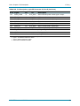
Table 2-4. Pin Descriptions, phyCORE-Connector X2, Row D
Pin # Signal
I/O
SL
Description
1D
VCC
I
3.15V
3.15V primary voltage supply input
2D
VCC
I
3.15V
3.15V primary voltage supply input
3D
GND
-
-
4D
VCC_AD_EXT
I
3.15V
µC ADC power supply input
5D
VCC_AD_EXT
I
3.15V
µC ADC power supply input
6D
N/C
-
-
Not connected
7D
N/C
-
-
Not connected
8D
WDI
I
3.15V
© PHYTEC America LLC 2009
Ground
Watchdog input. Connect this pin to an applicable signal to periodically reset the watchdog timer.
15
Part I, Chapter 2: Pin Description
L-714e_1
Table 2-4. Pin Descriptions, phyCORE-Connector X2, Row D (Continued)
Pin # Signal
I/O
SL
-
Description
9D
GND
-
Ground
10D
/RESIN
I
11D
N/C
-
-
Not connected
12D
N/C
-
-
Not connected
13D
N/C
-
-
Not connected
14D
GND
-
-
Ground
15D
N/C
-
-
Not connected
16D
U1_RX
I
3.15V
µC signal U1_RX/CAP1.0
17D
U1_TX
O
3.15V
µC signal U1_TX
18D
GPO_20
O
1.8V
µC signal GPO_20
19D
GND
-
-
20D
/RS232_EN
I
3.15V
UART 5/UART 1 RS-232 transceiver enable input. This
signal has an internal 100k pull-down.
21D
RS232_SD
I
3.15V
UART 5/UART 1 RS-232 transceiver shut down input.
This signal has an internal 100k pull-down.
22D
U1_RX_RS232
I
6.4Vb
U1_RX converted to RS-232 levels
23D
U1_TX_RS232
O
6.4Vb
U1_TX converted to RS-232 levels
3.0Va or 3.15V System reset input. Connect this pin to an open-drain
output and momentarily pull LOW to initiate a system
reset. Do not connect this pin to a push-pull output or
any other pull-up/pull-down circuitry.
Ground
24D
GND
-
-
25D
U3_DSR
I/O
3.15V
µC signal U3_DSR/U2_RX
Ground
26D
U3_DTR
O
3.15V
µC signal U3_DTR/U2_TX
27D
U3_RTS
O
3.15V
µC signal U3_RTS/U2_HRTS/GPO_23
28D
U3_RI
I
3.15V
µC signal U3_RI/GPI_11
29D
GND
-
-
Ground
30D
U6_IRRX
I
3.15V
µC signal U6_IRRX
31D
I2C2_SDA
I/O
1.8V
µC signal I2C2_SDA. This signal has an internal 2.2k
pull-up.
32D
I2C1_SDA
I/O
3.15V
µC signal I2C1_SDA. This signal has an internal 2.2k
pull-up.
33D
/RTC_INT
O
3.0V
Off-chip Real Time Clock interrupt alarm open-drain
output. This pin has an optional 100k internal pull-up.[3]
34D
GND
-
-
35D
ENET_TXN
O
Notec
Ethernet negative differential transmit output
36D
ENET_TXP
O
Notec
Ethernet positive differential transmit output
37D
ENET_CLKEN
I
3.15V
Ethernet clock enable. This pin has an internal 100k
pull-up. Ground this pin to disable the ethernet clock.
Typically this is used in a low power mode.
© PHYTEC America LLC 2009
Ground
16
Part I, Chapter 2: Pin Description
L-714e_1
Table 2-4. Pin Descriptions, phyCORE-Connector X2, Row D (Continued)
Pin # Signal
I/O
SL
Description
38D
GPIO_1
I/O
3.15V
39D
GND
-
-
40D
GPI_7
I
3.15V
µC signal GPI_07/PCAP3.0. This signal is used as the
SDIO controller interrupt input and has an internal 10k
pull-up.
41D
GPO_1
O
1.8V
µC signal GPO_01
42D
GPO_4
O
3.15V
µC signal GPO_04
43D
GPO_11
O
3.15V
µC signal GPO_11
44D
GND
-
-
45D
GPO_17
O
3.15V
µC signal GPO_17
46D
USB_ID
I
Noted
USB OTG ID pin. Normally this pin is connected
directly to the ID pin on an OTG connector.
47D
USB_D+
I/O
Noted
USB positive differential input/output
48D
USB_D-
I/O
Noted
USB negative differential input/output
49D
GND
-
-
50D
MOSI0
I/O
3.15V
µC signal MOSI0/SPI1_DATIO
51D
GPI_4
I
3.15V
µC signal GPI_04/SPI1_BUSY
52D
ONSW
O
1.2V
µC signal ONSW
53D
N/C
-
-
Not connected
54D
GND
-
-
Ground
55D
I2SRX_CLK1
I/O
3.15V
µC signal GPIO_01
Ground
Ground
Ground
µC signal I2SRX_CLK1/P0.0
56D
I2SRX_SDA1
I
3.15V
µC signal I2SRX_SDA1/HSTIM_CAP/GPI_06
57D
I2SRX_WS1
I/O
3.15V
µC signal I2SRX_WS1/P0.1
58D
ENET_COL
I
3.15V
µC signal ENET_COL/KEY_COL7/GPI_09
59D
GND
60D
ENET_MDC
-
-
I/O
3.15V
µC signal ENET_MDC/KEY_ROW6/GPIO_02
61D
Ground
ENET_RX_DV
I
3.15V
µC signal ENET_RX_DV/SPI2_BUSY/KEY_COL6/
GPI_08
62D
ENET_REF_CL
K
I
3.15V
µC signal ENET_REF_CLK/ENET_RX_CLK/
KEY_COL1
63D
ENET_TX_CLK
I
3.15V
µC signal ENET_TX_CLK/KEY_COL0
64D
GND
-
-
Ground
65D
ENET_RXD0
I
3.15V
µC signal ENET_RXD0/KEY_COL4
66D
ENET_TXD2
I/O
3.15V
µC signal ENET_TXD2/KEY_ROW1
67D
ENET_TXD1
I/O
3.15V
µC signal ENET_TXD1/KEY_ROW5
68D
TST_CLK2
O
3.15V
µC signal TST_CLK2
69D
GND
-
-
70D
/SDIO_WP
I
VCC_SDIO
© PHYTEC America LLC 2009
Ground
SDIO controller write protect input. This pin has an
internal 100k pull-up.
17
Part I, Chapter 2: Pin Description
L-714e_1
Table 2-4. Pin Descriptions, phyCORE-Connector X2, Row D (Continued)
Pin # Signal
I/O
SL
Description
71D
SDIO_POW0
O
VCC_SDIO
SDIO controller power control signal 1 output
72D
SDIO_CLK
O
VCC_SDIO
SDIO controller clock output
73D
SDIO_D0
I/O
VCC_SDIO
SDIO controller data 0 input/output
74D
GND
-
-
75D
SDIO_D3
I/O
VCC_SDIO
SDIO controller data 3 input/output
76D
SDIO_D5
I/O
VCC_SDIO
SDIO controller data 5 input/output
77D
SDIO_D6
I/O
VCC_SDIO
SDIO controller data 6 input/output
78D
TS_YOUT
I/O
-
µC signal TS_YOUT
79D
AGND
-
-
Analog ground
80D
ADIN2
I
3.15V
a.
b.
c.
d.
Ground
µC signal ADIN2
3.0V is the standard phyCORE-LPC3250 SOM configuration.
Typical -- see ADM3307 datasheet for details.
See the LAN8700I datasheet for details.
See the ISP1301 datasheet for details.
© PHYTEC America LLC 2009
18
Part I, Chapter 3: Jumpers
L-714e_1
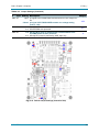
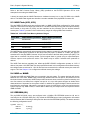
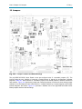
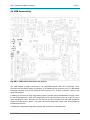
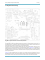
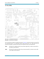
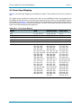
3 Jumpers
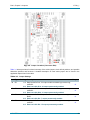
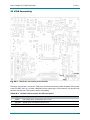
For configuration purposes, the phyCORE-LPC3250 has 24 solder jumpers, some of which have been
installed prior to delivery. Figure 3-1 and Figure 3-2 indicate the location of the solder jumpers on the
board. There are 11 solder jumpers located on the top side of the module (opposite side of connectors)
and 13 solder jumpers on the bottom side.
If manual jumper modification is required be sure to pay special attention to the "TYPE" column to ensure
you are using the correct type of jumper (0 Ohms, 10k Ohms, etc…). All jumpers are 0805 package with a
1/8W or better power rating.
Three and four position jumpers have pin 1 marked with a GREEN pad.
Fig. 3-1. Jumper Locations (Controller Side)
© PHYTEC America LLC 2009
19
Part I, Chapter 3: Jumpers
L-714e_1
Fig. 3-2. Jumper Locations (Connector Side)
Table 3-1 below provides a functional summary of the solder jumpers, their default positions, and possible
alternative positions and functions. A detailed description of each solder jumper can be found in the
applicable chapter listed in the table.
Table 3-1. Jumper Settings
J
Type Setting Description
J1
0R
J2
J3
J4
0R
0R
0R
Chapter
1+2 Data bus buffer D16...23 output enable controlled by processor signal BLS2.
2+3 Data bus buffer D16...23 output permanently enabled.
13
1+2 Data bus buffer D24...31 output enable controlled by processor signal BLS3.
2+3 Data bus buffer D24...31 output permanently enabled.
13
1+2 Data bus buffer D0...7 output enable controlled by processor signal
BLS0.
2+3 Data bus buffer D0...7 output permanently enabled.
13
1+2 Data bus buffer D8...15 output enable controlled by processor signal BLS1.
2+3 Data bus buffer D8...15 output permanently enabled.
13
© PHYTEC America LLC 2009
20
Part I, Chapter 3: Jumpers
L-714e_1
Table 3-1. Jumper Settings (Continued)
J
Type Setting Description
J5
0R
J6
0R
1+2 NAND Flash write protected during power-up, power-fail, and
power-down events by the controller /RESOUT signal.
2+3 NAND Flash permanently write protected.
2+4 NAND Flash write protection controlled via GPO_19.
Open NAND Flash permanently write enabled.
1+2 Activating /RESIN produces a system /RESET_SYS event.
2+3 Activating /RESIN produces a system /RESET_SYS and a /
RESET_BAT event.
Chapter
9.2
N/A
J7
10k
Open Ethernet PHY operation MODE0 bit = 1.
Closed Ethernet PHY operation MODE0 bit = 0.
10.2
J8
10k
Open Ethernet PHY operation MODE1 bit = 1.
Closed Ethernet PHY operation MODE1 bit = 0.
10.2
J9
10k
Open Ethernet PHY operation MODE2 bit = 1.
Closed Ethernet PHY operation MODE2 bit = 0.
10.2
Open µC signal SSEL0 disconnected from on-board SPI EEPROM /CS0
input.
Closed µC signal SSEL0 connected to on-board SPI EEPROM /CS0
input.
9.5
J16 0R
J17 0R
J19 0R
J21 0R
Open Watchdog extended mode selected. Timeout period ~6s.
Closed Watchdog normal mode selected. Timeout period ~12ms.
1+2 External watchdog reset forces a system wide reset and sleep
reset.
2+3 External watchdog reset forces a system wide reset.
1+2 External memory bus voltage set to 1.8V.
2+3 External memory bus voltage set to 3.15V.
7
7
13.1
J22 0R
Open Voltage regulator U22 disconnected from VCC_RTC.
Closed Voltage regulator U22 supplies VCC_RTC power.
4.5.3
J23 0R
Open Voltage regulator U22 disconnected from VCC_SDRAM.
Closed Voltage regulator U22 supplies VCC_SDRAM power.
4.5.3
J24 0R
Open Voltage regulator U23 disconnected from VCC_SDRAM.
Closed Voltage regulator U23 supplies VCC_SDRAM power.
4.5.1
J25 0R
Open Voltage regulator U23 disconnected from VCC_1V8.
Closed Voltage regulator U23 supplies VCC_1V8 power.
4.5.1
J26 0R
Open Voltage regulator U23 disconnected from VCC_RTC.
Closed Voltage regulator U23 supplies VCC_RTC power.
4.5.1
J27 0R
Open Voltage regulator U23 disconnected from VCC_CORE.
Closed Voltage regulator U23 supplies VCC_CORE power.
4.5.1
J28 0R
Open Voltage regulator U23 disconnected from VCC_1V2.
Closed Voltage regulator U23 supplies VCC_1V2 power.
4.5.1
J29 0R
Open Voltage regulator U27 disconnected from VCC_CORE.
Closed Voltage regulator U27 supplies VCC_CORE power.
4.5.2
© PHYTEC America LLC 2009
21
Part I, Chapter 3: Jumpers
L-714e_1
Table 3-1. Jumper Settings (Continued)
J
Type Setting Description
J30 0R
Open µC signal LCD17/HIGHCORE disconnected from core voltage control.
Closed µC signal LCD17/HIGHCORE controls core voltage setting
(0.9V or 1.2V).
J31 10k
1+2 SPI EEPROM write enabled.
2+3 SPI EEPROM write protected.
J32 0R
1+2 Off-chip RTC power is automatically selected between VCC
and VBAT based on VCC presence.
2+3 Off-chip RTC power is powered by VBAT input only.
Chapter
4.5.2
9.5
6
Fig. 3-3. Default Jumper Settings (Controller Side)
© PHYTEC America LLC 2009
22
Part I, Chapter 3: Jumpers
L-714e_1
Fig. 3-4. Default Jumper Settings (Connector Side)
© PHYTEC America LLC 2009
23
Part I, Chapter 4: Power
L-714e_1
4 Power
The phyCORE-LPC3250 operates off of four separate power supply input domains. For systems that do
not required maximum flexibility it is possible to operate the phyCORE-LPC3250 off of a single power
supply voltage.
The following sections of this chapter discuss the primary power pins on the phyCORE-Connector X2 in
detail.
4.1 Primary System Power (VCC)
The phyCORE-LPC3250 operates off of a primary voltage supply with a nominal value of 3.15V. On-board
switching regulators generate the 1.8V, and 1.2V, and adjustable 0.9-1.2V voltage supplies required by the
LPC3250 MCU and on-board components from the primary 3.15V supplied to the SOM.
For proper operation the phyCORE-LPC3250 must be supplied with a voltage source of 3.15V ± 0.1V at
the VCC pins on the phyCORE-Connector X2. See Table 2-1 for VCC pin locations. See Chapter 14 for
current requirements.
Connect all +3.15V VCC input pins to your power supply and at least the matching number of GND pins
neighboring the +3.15V pins.
CAUTION:
As a general design rule we recommend connecting all GND pins neighboring signals which are being
used in the application circuitry. For maximum EMI performance all GND pins should be connected to a
solid ground plane.
4.2 Secondary Battery Power (VBAT)
For applications requiring a low power deep sleep mode a secondary battery sleep supply with a nominal
value of 3.0V is required. The battery supply powers the SDRAM and RTCs during a sleep condition,
allowing primary system power (VCC) to be removed.
For deep sleep operation the phyCORE-LPC3250 must be supplied with a secondary voltage source of
3.0V ± 0.1V at the VBAT pin on the phyCORE-Connector X2. See Table 2-1 for the VBAT pin location. See
Chapter 14 for current requirements.
Applications not requiring a sleep mode can connect the VBAT pin to the primary system power supply
(VCC = 3.15V).
4.3 Analog-to-Digital Converter Power (VCC_AD_EXT)
The LPC3250 Analog-to-Digital converter power domain pins are brought out to the phyCORE-Connector
X2 for an optional external filtered power supply. See Table 2-1 for the VCC_AD_EXT pin location. See the
NXP LPC3250 datasheet for permissible input voltage ranges (2.7V to 3.3V as of the printing of this
manual).
In general the VCC_AD_EXT pins will be connected to the primary VCC = 3.15V supply, requiring no
special circuitry. The phyCORE-LPC3250 Carrier Board connects the VCC_AD_EXT pins through a 1R/
4.7uF filter network from the primary VCC = 3.15V supply. Refer to the phyCORE-LPC3250 Carrier Board
schematics for details.
© PHYTEC America LLC 2009
24
Part I, Chapter 4: Power
L-714e_1
4.4 SDIO Controller Power (VCC_SDIO)
The on-board SDIO controller is capable of a configurable interface voltage to meet the demands of the
variety of SDIO devices with varying power requirements. In addition the SDIO controller is capable of
switching between a high power and low power mode on-the-fly to optimize dynamic power consumption.
The SDIO controller interface voltage is powered and set via the VCC_SDIO pins on the phyCOREConnector X2. The high/low power switching is controlled via the SDIO_POW0 and SDIO_POW1 pins on
the phyCORE-Connector X2. See the NXP SDIO101 datasheet for details on these power mode control
pins. See Table 2-1 for the locations of the applicable SDIO power and control pins.
For applications requiring an adjustable SDIO supply voltage the VCC_SDIO pins must be supplied with a
voltage of 2.25-3.6V1. See Chapter 14 for current requirements. See the phyCORE-LPC3250 Carrier
Board schematics for example adjustable supply circuitry. For SDIO applications which can operate off of
3.15V the VCC_SDIO pins can be connected directly to the VCC power supply and the SDIO_POW0/1
pins can be left unconnected.
4.5 On-board Voltage Regulators
The phyCORE-LPC3250 provides three on-board switching regulators to source the 1.2V, 1.8V, and
adjustable 0.9-1.2V voltages required by the processor and on-board components. Figure 4-1 presents a
graphical depiction of the powering scheme. The jumpers in blue are by default populated, while the
jumpers in white are unpopulated. By default U27 powers the VCC_CORE rail with an adjustable supply,
U22 powers the VCC_RTC and VCC_SDRAM rails, and U23 powers the VCC_1V2 and VCC_1V8 rails.
Notice that U22 generates 1.2V and 1.8V just as does U23. The reason for this is that U22 continues to
power the RTC and SDRAM subsystems via backup battery during a sleep mode. See Chapter 5 for
details.
To reduce system costs U27 and U22 can be removed. To supply the power lost by the removal of these
two regulators J26, J27, and J24 must be closed. Figure 4-1 depicts the standard default configuration, but
custom configurations can also be ordered. If your system does not require an adjustable core voltage to
periodically lower core power consumption while keeping the system powered then U27 can be removed
and J27 can be closed (note that the core is fixed at 1.2V in this case). If your system is not power
conscious and does not need to enter a sleep mode during moments of processor inactivity to conserve
power then U23 can be removed and J26 and J24 can be closed. This multi regulator + jumper approach
provide cost and system requirement flexibility.
The following sections go into detail about each switching regulator and any associated configuration
jumpers.
1. See the NXP SDIO101 datasheet for details.
© PHYTEC America LLC 2009
25
Part I, Chapter 4: Power
U27
U22
L-714e_1
0.9-1.2V
J29
1.2V
J22
1.8V
J23
1.2V
J26
J27
U23
J28
1.8V
J24
VCC_1V8
VCC_1V2
VCC_CORE
VCC_RTC
VCC_SDRAM
J25
Fig. 4-1. phyCORE-LPC3250 On-board Powering Scheme
4.5.1 Primary 1.2V and 1.8V Supplies (U23)
The dual output switching regulator located at U23 generates the 1.2V and 1.8V core and peripheral
supplies required by system components from the primary VCC = 3.15V board supply. Various jumpers
have been provided as current measurement access points on the outputs of both of these supplies. Table
4-1 provides a summary of the jumpers and their operation. See Chapter 4.5.4 for current measurement
techniques with a precision shunt resistor.
Table 4-1. U23 1.2V/1.8V Primary Voltage Regulator Jumper Settings
J
Type Setting Description
J24 0R
Open Voltage regulator U23 disconnected from VCC_SDRAM.
Closed Voltage regulator U23 supplies VCC_SDRAM power. Do not close this unless
U22 is unpopulated.
J25 0R
Open Voltage regulator U23 disconnected from VCC_1V8.
Closed Voltage regulator U23 disconnected from VCC_1V8.
J26 0R
Open Voltage regulator U23 disconnected from VCC_RTC.
Closed Voltage regulator U23 supplies VCC_RTC power. Do not close this unless U22
is unpopulated.
J27 0R
Open Voltage regulator U23 disconnected from VCC_CORE.
Closed Voltage regulator U23 supplies VCC_CORE power. Do not close this unless
U22 is unpopulated.
J28 0R
Open Voltage regulator U23 disconnected from VCC_1V2.
Closed Voltage regulator U23 supplies VCC_1V2 power.
© PHYTEC America LLC 2009
26
Part I, Chapter 4: Power
L-714e_1
4.5.2 Adjustable Core Voltage Supply (U27)
The single output switching regulator located at U27 generates the adjustable 0.9V to 1.2V core supply to
the processor from the primary VCC = 3.15V board supply. The regulator's output voltage is controlled by
the processor's HIGHCORE signal (labeled as net LCD17). To set the core voltage to 0.9V set the
HIGHCORE signal HIGH. To set the core voltage to 1.2V set the HIGHCORE signal LOW. The
HIGHCORE signal can be automatically managed or manually controlled via the LPC3250 power
management registers. See the LPC3250 User Manual for details.
Because the HIGHCORE signal is multiplexed with other peripherals, jumper J30 has been provided to
allow disconnection of the HIGHCORE signal from controlling the core regulator output voltage. When J30
is disconnected the core regulator is fixed at 1.2V. This jumper is provided as a prototyping convenience.
In practice an unneeded additional cost would be added by simply ordering a SOM configuration in which
J30 is removed. If J30 is removed then the regulator is fixed at 1.2V and therefore an adjustable supply is
no longer needed and instead can be satisfied by the dual 1.2V/1.8V regulator U23 through additional
jumper configurations. A SOM without the need for an adjustable core would have U27 removed and J27
closed.
Output jumper J29 has been provided as current measurement access points for this supply. See Chapter
4.5.4 for current measurement techniques with a precision shunt resistor.
4.5.3 SDRAM and RTC Supplies (U22)
The dual output switching regulator located at U23 generates the 1.2V and 1.8V RTC and SDRAM
supplies required by the RTC and SDRAM. U23 gets its input power from the output of the battery switch
located at U19. The battery switch is responsible for connecting VCC to the input of U23 during normal
operating conditions (VCC is present) and VBAT to the input of U23 during sleep operations (VCC is shut
down). This switchover between VCC and VBAT is automatic. Output jumpers have been provided as
current measurement access points for both of these supplies. Table 4-2 provides a summary of the
jumpers and their operation. See Chapter 4.5.4 for current measurement techniques with a precision shunt
resistor.
Table 4-2. U22 RTC/SDRAM Voltage Regulator Jumper Settings
J
Type Setting Description
J22 0R
Open Voltage regulator U22 disconnected from VCC_SDRAM.
Closed Voltage regulator U22 supplies VCC_SDRAM power.
J23 0R
Open Voltage regulator U22 disconnected from VCC_RTC.
Closed Voltage regulator U22 supplies VCC_RTC power.
4.5.4 Selecting Shunt Resistors for Current Measurements
To make current measurements the 0 Ohm resistors populating the regulator output jumpers should be
replaced by precision shunt resistors allowing the current draw to be calculated from the voltage
measurement taken across the shunt resistor. When selecting a shunt resistor it is desirable to select a
resistor large enough to give a voltage measurement that is not overtaken by noise. However, a larger
shunt resistor means a larger voltage drop across the shunt resulting in a smaller output voltage. The
output voltage after the shunt should be kept above the reset threshold. If the shunt resistor is too large the
voltage at the output could be below the supervisor reset threshold and force the system into reset. A good
starting place is a 0.025 Ohm precision shunt in a 0805 package.
© PHYTEC America LLC 2009
27
Part I, Chapter 4: Power
L-714e_1
4.6 Voltage Supervisor (U16, U17)
The phyCORE-LPC3250 comes equipped with two triple voltage supervisor IC's located at U16 and U17.
These voltage supervisors are responsible for monitoring all on-board supply voltages (with the exception
of the adjustable core supply voltage which is not monitored) and issuing a system reset during a powerup, power-fail, or power-down event.
U16 is the primary system supervisor which is responsible for monitoring the primary system supply
voltage VCC = 3.15V, the fixed VCC_1V8 = 1.8V peripheral supply voltage, and the fixed VCC_1V2 = 1.2V
core supply voltage. When any of the three supplies dip below their nominal reset threshold voltages for a
predetermined amount of time the /RESET_SYS signal is asserted LOW for the duration of the power fail
event and is held low for an additional 200ms1 after the power fail event has cleared. The nominal reset
thresholds for U16 are set at:
Table 4-3. Primary System Supervisor Reset Thresholds
Supply Voltage Nominal Reset Threshold
VCC (3.15V)
3.0V
VCC_1V8 (1.8V)
1.7V
VCC_1V2 (1.2V)
1.1V
U17 is the sleep mode supervisor and is responsible for monitoring the VBAT = 3.0V input voltage, the
VCC_SDRAM = 1.8V SDRAM supply voltage, and the VCC_RTC = 1.2V supply voltage. When any of the
three supplies dip below their nominal reset threshold voltages for a predetermined amount of time the /
RESET_BAT and /RESET_SYS signals are asserted LOW for the duration of the power fail event and are
held low for an additional 200ms1 after the power fail event has cleared. The nominal reset thresholds for
U17 are set at:
Table 4-4. Sleep System Supervisor Reset Thresholds
Supply Voltage
Nominal Reset Threshold
VBAT (3.0V)
2.8V
VCC_SDRAM (1.8V) 1.7V
VCC_RTC (1.2V)
1.1V
The dual supervisor approach allows the creation of two separate reset signals: the system reset signal /
RESET_SYS, and the sleep reset signal /RESET_BAT. The primary system supervisor U16 is capable of
issuing a system reset via the /RESET_SYS signal while the sleep supervisor U17 is capable of issuing a
sleep reset via the /RESET_BAT signal in addition to a system reset via the /RESET_SYS signal. This
method allows: (1) the processor to always be held in reset (via /RESET_SYS) when main system power is
removed and (2) the detection of a power fail event during a sleep condition via the /RESET_BAT signal.
Condition (1) is required any time power is reapplied to the processor to ensure proper system startup after
the reapplication of power. Condition (2) allows for additional external deep sleep/power control logic to be
reset during a power fail event on the battery supplies (VBAT, VCC_RTC, or VCC_SDRAM). Since the
LPC3250 does not provide sleep registers (however the on-chip RTC SRAM could potentially double for
this) that are powered during a sleep condition the LPC3250 must rely on another method of determining it
was in a sleep state upon a wake event. This could be done via writing a special code in the RTC scratch
pad SRAM before entering sleep (a key value that indicates you were in sleep), however, a momentary fail
on the supply could potentially corrupt SRAM in an area that did not affect the key or corrupt sections of
SDRAM which are undetectable. In this instance the system would resume from a sleep condition where
1. Typical reset period. See Maxim IC MAX6710 datasheet for details.
© PHYTEC America LLC 2009
28
Part I, Chapter 4: Power
L-714e_1
data was corrupted, but have no method of determining so, resulting in a possible processor lockup. To
prevent this from happening external sleep circuitry should be used which remembers the sleep state and
is reset via the /RESET_BAT signal should a sleep supply (VBAT, VCC_RTC, VCC_SDRAM) fail.
© PHYTEC America LLC 2009
29
Part I, Chapter 5: Deep Sleep
L-714e_1
5 Deep Sleep
The phyCORE-LPC3250 was designed to support a "deep sleep" mode where all primary system power is
removed, leaving only a battery backup supply powering essential sleep functions. This mode was
designed for ultra low power to extend primary system battery life in power critical applications. Note that
this mode assumes the use of a battery as the primary system power source, but is not required. A wall
adapter, or other power source can also be used but it is more typical that low power consumption is
required when operating the system from a battery supply to maximize battery life.
Figure 5-1 depicts a typical sleep enabled powering system where the entire system is powered from a
battery. The battery is then regulated to 3.15V, 3.3V, and 3.0V to satisfy the necessary power inputs to the
phyCORE-LPC3250. Control logic is responsible for enabling and disabling primary system power (VCC
and VCC_SDIO), while the secondary battery voltage VDS remains continuously.
Under normal operating conditions S1 will be closed and the system will be powered up. The user will
initiate a sleep event by pressing the Power Button. The phyCORE-LPC3250 will detect the press of the
power button and begin a sleep sequence in software preparing the system for the removal of primary
power. The last step in the sleep sequence will be the phyCORE-LPC3250 signaling the Control Logic to
shut down the external power supplies by opening switch S1. The only parts of the system that remain
powered during a deep sleep condition are the on-board SDRAM, on-chip RTC, off-chip RTC, and sleep
Control Logic. All four subsystems are powered by the 3.0V supply during a sleep event, drawing minimal
power.
Once in sleep there are three different methods to wake the system and resume normal operation. These
methods are: (1) an on-chip RTC alarm event via the ONSW signal or (2) an off-chip RTC alarm event via
the /RTC_INT signal or (3) a user initiated wake event via the Power Button. Any three of these signals can
trigger the Control Logic to reapply power to the system via closing S1. In addition to power control, the
Control Logic also remembers the sleep state. Upon system reboot during a wake event the processor can
check the sleep state to determine if the system should have a fresh boot or take the necessary steps to
resume from a sleep condition. The Control Logic sleep state can only be cleared by either the processor,
or a power fail event during sleep via the /RESET_BAT signal. In this manor should the power fail during a
sleep event the processor can begin a normal boot sequence on reapplication of power due to the possibly
corrupted memory data caused by the power fail condition.
Fig. 5-1. Typical phyCORE-LPC3250 Sleep Enabled Powering Scheme
© PHYTEC America LLC 2009
30
Part I, Chapter 5: Deep Sleep
L-714e_1
The on-board battery switch U19 is responsible for automatically powering the SDRAM and RTC
subsystems from the VBAT input when VCC is lost. Under normal operating conditions (when VCC is
present) the RTC and SDRAM domains are powered by the VCC supply. See the Texas Instruments
TPS2115 battery switch datasheet for more details.
For a detailed explanation of the sleep control circuitry on the phyCORE-LPC3250 Carrier Board see
Chapter 23.
© PHYTEC America LLC 2009
31
Part I, Chapter 6: External RTC (U26)
L-714e_1
6 External RTC (U26)
An external RTC (RTC-8564JE) located at U26 has been provided in addition to the LPC3250 on-chip
RTC. This RTC provides a secondary time keeping source, along with a secondary alarm mechanism to
the processor via the /RTC_INT signal. By default the /RTC_INT signal is used on the phyCORE-LPC3250
Carrier Board to wake-up the power system during a deep sleep.
The RTC is interfaced to the processor via the I²C1 port. The default I²C address of the device is binary
1010 001x, where the 'x' bit is the read/write operation bit.
The RTC is automatically powered via the VBAT power input during a sleep condition. Jumper J32 is
provided to configure the power source when the phyCORE-LPC3250 is ordered with a custom power
configuration. In this configuration the on-chip RTC and SDRAM do not need to be powered during sleep,
and only the external RTC is powered. This allows a reduced cost configuration with the removal of the
dual switching regulator U22 and battery switch IC U19. This is also the most power efficient method of
putting the system to sleep while allowing the external RTC to reawake the system at a later time. By
default J32 is set to the 1+2 position, connecting the RTC power to the VCC_BATT signal, used during the
more complex sleep mode that keeps the on-chip RTC and SDRAM alive. Alternatively this jumper can be
set to the 2+3 position for the ultra low power sleep mode where U22 and U19 are removed.
© PHYTEC America LLC 2009
32
Part I, Chapter 7: External Watchdog
L-714e_1
7 External Watchdog
An external Maxim MAX6301 watchdog located at U18 has been provided as a processor independent
means of system recovery in the event of a lockup. By default the watchdog is disabled. To enable the
watchdog circuit the WDI input at the phyCORE-Connector (see Table 2-1) must be taken out of Hi-Z.
When the phyCORE-LPC3250 SOM is mounted on the phyCORE-LPC3250 Carrier Board the watchdog
can be taken out of Hi-Z by closing an applicable jumper. See the phyCORE-LPC3250 Carrier Board
Chapter 38 for details on the jumper and associated settings. When closed processor signal GPO_20 is
connected to the WDI input of the watchdog circuit. Since GPO_20 is a push-pull output of the processor,
this connection effectively takes the WDI input out of Hi-Z and enables the watchdog. After the watchdog's
internal timer expires the open collector /RES output of the IC is pulled LOW. Jumper J19 connects the
watchdog IC's /RES output to either the /RESET_SYS signal, or the /RESET_BAT signal. By default J19 is
set to the 2+3 position, connecting the /RES output to the /RESET_SYS signal. Alternatively this jumper
can be set to the 1+2 position, connecting the /RES output to the /RESET_BAT signal.
Once enabled the watchdog WDI input must be toggled before the internal timeout period expires to
prevent the /RES output from going active. The nominal watchdog timeout period is set to 6 seconds and
can be adjusted down to 12 milliseconds by closing jumper J17. Leave J17 open to keep the watchdog
timeout period at 6 seconds.
The WDI input does not need to be pulsed with a HIGH or LOW going pulse, but instead the WDI input just
needs to change states before the timeout period expires.
Typically the processor will use an available timer interrupt to change the state of the WDI input (via
GPO_20 when used on the phyCORE-LPC3250 Carrier Board) before the watchdog timeout period
expires. In this manor should the processor lock up, the WDI input will no longer be toggled, the watchdog
timeout period will expire, and the watchdog will assert the /RES output causing a system reset restoring
processor operation.
© PHYTEC America LLC 2009
33
Part I, Chapter 8: System Configuration and Booting
L-714e_1
8 System Configuration and Booting
For operation of the phyCORE-LPC3250 several parts of the system should be initialized. Although very
little initialization needs to take place for the most basic operation, it is typical that the following interfaces
will be initialized:
1. Clocking and power
2. SDRAM
3. Boot map
Clocking and Power
After a reboot the processor is operating off of the main crystal at 13.0MHz. While sufficient for small
applications, it is most likely that at some point the need for full processor frequency will arise. To initialize
the primary clocking and power control the following registers must be set:
1. HCLKDIV_CTRL
2. HCLKPLL_CTRL
3. PWR_CTRL
Please refer to the "Clocking and Power Control" chapter of the NXP Semiconductors LPC3250 hardware
manual for details on setting these registers. Additionally you may refer to the example code provided on
the PHYTEC Spectrum CD.
SDRAM
After a reboot the SDRAM interface is reset and must be initialized. The initialization procedure involves
initializing two primary interfaces: 1) the LPC3250 SDRAM controller, and 2) the SDRAM itself.
Initialization of the LPC3250 SDRAM controller sets up the processor with the proper timing and size
configuration values required to interfaces the external SDRAM. The initialization of the SDRAM sets up
the "mode" and "extended mode" registers on the SDRAM with information such as burst length, burst
type, CAS latency, driver strength, etc... Example SDRAM initialization is code provided on the PHYTEC
Spectrum CD.
Boot Map
By default after a reboot the LPC3250 on-chip boot ROM is mapped to address 0x0000 0000 and internal
RAM (IRAM) is mapped to 0x0800 0000. The BOOT_MAP register controls remapping the IRAM to
address 0x0000 0000. Remapping of IRAM is required for interrupts to function correctly. The beginning of
IRAM is reserved for the interrupt vector table, and without proper remapping an interrupt will cause the
processor to jump to the on-chip boot ROM. Therefore one of the very first initialization steps should be to
set this register to 1 to remap IRAM to 0x0000 0000.
8.1 Boot Process and Boot Modes
The boot process for the LPC3250 is a multi-staged effort involving one or more boot loaders. At the very
least after a reset the LPC3250 on-chip boot ROM will execute either (1) the UART5 boot mode, or (2) the
normal boot mode. The boot mode is controlled by strapping the SERVICE_N signal of the processor
HIGH or LOW after a reset. On the phyCORE-LPC3250 this signal is labeled as /SERVICE. An on-board
pull-up resistor pulls this signal HIGH. However, when installed on the phyCORE-LPC3250 Carrier Board
the default boot configuration jumper connects the /SERVICE signal to GND.
In boot mode (1) the boot ROM attempts to boot code loaded over UART5 with a simple boot protocol. In
boot mode (2) the boot ROM first attempts to boot from the SPI port, followed by the external memory bus,
and finally from NAND Flash. Details of the boot protocol for each bootable source can be found in the
LPC3250 User's Manual.
© PHYTEC America LLC 2009
34
Part I, Chapter 8: System Configuration and Booting
L-714e_1
The most typical boot configuration will boot from NAND Flash. In this boot mode the boot ROM attempts
to copy boot code from block 0 or block 1 (block 1 if block 0 is bad) into IRAM and executes it. Since the
boot ROM can only copy code from block 0 or block 1, this limits the size of the secondary boot loader to
be constricted to stay within a single block in NAND Flash. For the phyCORE-LPC3250 NAND Flash this
limit is 16kBytes. In practice this is limited to 15.5kBytes for reasons which will become apparent in the
sections that follow.
The secondary boot loader is responsible for loading and executing a third level boot loader or application
code, depending on the complexity of the software design. For bare-metal applications the secondary boot
loader will likely suffice to load and execute the application. For operating systems the secondary boot
loader will likely load a more robust, feature rich boot loader such as Das U-Boot, or E-Boot.
The job of a basic secondary boot loader can be summarized as the following:
1.
2.
3.
4.
Initialize the Clocking and Power (bump the core up to 208MHz)
Initialize the SDRAM
Copy the remaining code from NAND Flash into SDRAM
Transfer execution to SDRAM
Before covering the structure of the secondary boot loader and application code in NAND Flash, a short
description of the structure of the external SLC NAND Flash device used on the phyCORE-LPC3250 is
presented.
The external SLC NAND Flash used on the phyCORE-LPC3250 is a "small page" device consisting of
"blocks" and "pages" of data. The NAND Flash is divided into blocks which are 16kB in size. Each block
consists of 32 pages which are 512 bytes in size + 16 bytes of "spare" area. The spare area is used to (1)
store bad block information, and (2) store error correction data. Unlike NOR Flash, NAND Flash can
contain "bad blocks" within the Flash device. These are blocks which 1 or more bits within the block can no
longer be reliably written and read. Therefore the entire block is marked bad and should not be used.
NAND Flash devices are shipped with BLOCK 0 guaranteed to be a good block. Each individual NAND
device may contain 0 or more bad blocks from the manufacturer, and more bad blocks may develop over
time through write/erase operations. Bad blocks in new NAND devices are marked by the manufacturer by
writing a value other than 0xFF to the 6th byte of the spare area of the first page of each block. For
example, if the 6th byte of the spare area of block 12, page 0 did not contain 0xFF, this would indicate it is
a bad block. Figure 8-1 shows a graphical representation of the organization of the NAND Flash structure.
© PHYTEC America LLC 2009
35
Part I, Chapter 8: System Configuration and Booting
L-714e_1
Fig. 8-1. Small Page SLC NAND Flash Structure
In addition to the spare area being used to mark bad blocks, it is also used by the LPC3250 NAND Flash
controllers to store error correction code (ECC) data. With this technique an integrity check between the
data within the page and the ECC can be made to determine if the data is good (given that bad blocks can
develop over time).
Now that a better understanding of the NAND structure has been presented a detailing of the code
structure which resides in NAND Flash can be presented.
The code in NAND Flash will have one of three structures: (1) application that is 15.5kB in size or less, (2)
boot loader + application that is 256kB in size or less, or (3) boot loader + application that exceeds 256kB
in size.
In (1) the code is small enough to fit and execute in IRAM and remains in block 0. It must fit in block 0
because the LPC3250 boot loader ROM will only load data from block 0.
In (2) the code exceeds block 0 in size and must occupy more NAND Flash. In this case a secondary boot
loader is needed to load the application code beyond block 0 into IRAM and execute it. The secondary
boot loader is placed in block 0. The application is placed in block 1 or beyond.
In (3) the code exceeds IRAM size and must be placed in SDRAM. In this case a secondary boot loader is
placed in block 0 and is responsible for initializing SDRAM, loading the application code beyond block 0
into SDRAM, and then transferring execution to SDRAM.
In all three instances above block 0 page 0 always contains special data. It is for this reason that the boot
loader is restricted to 15.5kB in size instead of 16kB. The block 0/page 0 data consists of the ICR, size
information, and block 0 bad block information. This information is needed by the LPC3250 boot ROM to
find out what type of NAND Flash the controller will be interfacing, how much code to copy from NAND
© PHYTEC America LLC 2009
36
Part I, Chapter 8: System Configuration and Booting
L-714e_1
Flash into IRAM, and if this block is a bad block and the boot information is contained in block 1 instead.
See the NXP Semiconductors LPC3250 hardware manual for a detailed explanation of the required data in
block 0 page 0 of the NAND Flash.
Typically applications will require (3) above. In this case the boot process becomes:
1. The controller is reset.
2. The LPC3250 boot loader ROM executes and loads the secondary boot loader code located in
block 0 of the NAND Flash into IRAM and transfers execution to it.
3. The secondary boot loader initializes the clocks and SDRAM.
4. The secondary boot loader copies the application code from NAND Flash starting at block 1 (or
beyond) into SDRAM and transfers execution to it.
At this point the primary application is running. For most applications not involving an operating system this
is all that is needed. It is possible that this application could be yet another boot loader that is responsible
for booting an operating system such as Linux or WinCE.
To simplify and enhance the boot process the phyCORE-LPC3250 comes pre-flashed with a special boot
loader written by NXP. This boot loader, called the "Stage 1 Loader" is discussed in more detail in the
follow section.
8.1 Stage 1 Loader
The Stage 1 Loader (S1L) is a robust third level boot loader written by NXP Semiconductor to simplify and
enhance the LPC3250 booting procedure. The S1L is feature rich with the ability to configure clocking,
virtual memory mapping, data and instruction caches, the ability to access NAND flash, and the ability to
boot applications/images from the NAND flash, SD Card, or serial port to name a few of the features the
S1L provides.
In general the S1L is used to execute applications or, a 4th level boot loader such as Das U-Boot or EBoot. The PHYTEC Rapid Development Kit comes with a pre-loaded SD Card containing demo
applications, a Windows CE image, and a Linux image to easy facilitate the evaluation of each operating
system as well as stand alone "bare metal" applications without the need for a debugger/JTAG probe.
Kickstart Loader
As noted in the previous section the secondary boot loader residing in NAND flash must be 15.5kB in size
or less in order for the LPC3250 on-chip boot ROM to successfully load and execute the image. The robust
functionality that the S1L provides cannot be packed into such a small Flash footprint, and instead exceeds
the 15.5kB required for a secondary boot loader on the LPC3250. To get around this limitation the S1L is
loaded as 3rd level boot loader by a small, compact secondary boot loader called the Kickstart Loader. The
Kickstart Loader written by NXP fits within the 15.5kB constraints of the boot ROM and is executed
immediately after a processor reset (provided UART5 booting isn't enabled or successful, and SPI and
EMC booting fail).
Once the Kickstart Loader is executing it relocates itself to the top 16kB of IRAM, leaving 240KB of IRAM
space left (starting at address 0x0) for an application, or 3rd level boot loader. The Kickstart Loader then
loads code starting at Flash block 1 into IRAM and transfers execution to it.
On the phyCORE-LPC3250 this application/3rd level boot loader is the S1L. The S1L, once executed,
provides a menu/configuration interface via UART5 of the processor.
Accessing the Stage 1 Loader
© PHYTEC America LLC 2009
37
Part I, Chapter 8: System Configuration and Booting
L-714e_1
To access the Stage 1 Loader connect your PC to the bottom DB-9 female RS-232 connector on the
phyCORE-LPC3250 Carrier Board at connector P1. Configure a terminal communications application for
115200,8,n,1, no hardware flow control on your PC. Press the system reset button S1 on the Carrier board
to force a system reset. The terminal window should begin display S1L output. Press any key to stop the
auto boot procedure (if one is configured, otherwise the S1L will go to the phy3250> prompt by itself) and
come to the phy3250> prompt. Type help menu to get a list of commands. For further instructions on using
the S1L and executing demo applications, refer to the appropriate Quickstart guides provided on the
PHYTEC Spectrum CD.
Boot Sequence
1. The boot sequence with the Kickstart Loader and Stage 1 Loader is as follows:
2. Controller is reset
3. On-chip boot ROM executes and loads the Kickstart Loader from NAND block 0 into IRAM at
address 0 and executes it
4. Kickstart Loader relocates itself to the upper 16kB of IRAM
5. Kickstart Loader begins reading the NAND Flash at block 1 and loading code (in this case, the
Stage 1 Loader) starting at address 0x0 in IRAM. The first page of block 1 contains the size of the
code to be loaded.
6. The Kickstart transfers execution to the loaded application code (S1L) at address 0
7. The Stage 1 Loader executes and either stops at the S1L prompt, or continues to boot from the
terminal interface, SD card, or NAND flash depending on the auto boot configuration.
Where To Find More Information
In addition to the help menus NXP has published a document detailing the Kickstart Loader and the Stage
1 Loader. Please refer to this document, located on your PHYTEC Spectrum CD in PHYTEC\phyCORELPC3250\Documentation\Stage1 Loader, for more information regarding these boot loaders.
© PHYTEC America LLC 2009
38
Part I, Chapter 9: System Memory
L-714e_1
9 System Memory
The phyCORE-LPC3250 provides four types of on-board memory:
1.
2.
3.
4.
SDR SDRAM (U10/U11):
NOR Flash (U12/U13):
NAND Flash (U8):
EEPROM (U9):
from 16MB to 128MB
from 1MB to 8MB
from 16MB to 128MB
from 1KB to 32KB
The following sections of this chapter detail each memory type used on the phyCORE-LPC3250 SOM.
9.1 SDRAM (U10, U11)
The phyCORE-LPC3250 comes pre-configured with 16, 32 or 64MB of 133MHz SDR SDRAM configured
for 32-bit access using two 16-bit wide RAM chips at U10 and U11.
The LPC3250 is capable of addressing a single RAM bank located at memory address 0x8000 0000 and
extending to 0x9FFF FFFF via the /DYCS0 signal. It should be noted that this is beyond what the
phyCORE-LPC3250 supplies for on-board memory. Refer to Table 9-1 for permissible SDRAM memory
access ranges.
Table 9-1. Valid SDRAM Memory Address Ranges
SDRAM Size Lower Memory Address Upper Memory Address
16MB
0x8000 0000
0x80FF FFFF
32MB
0x8000 0000
0x81FF FFFF
64MB
0x8000 0000
0x83FF FFFF
128MB
0x8000 0000
0x87FF FFFF
The second SDRAM memory bank located on /DYSC1 is not used on the phyCORE-LPC3250. Accesses
to this region of memory should not be performed.
9.2 NAND Flash (U8)
The NAND memory is comprised of a single 16MB to 128MB chip located at U8 and is interfaced via the
LPC3250 NAND memory bus. Write protection control of the NAND device is configurable via jumper J5.
Table 9-2 lists the various NAND Flash write protection control options, including the default setting on the
kit version of the phyCORE-LPC3250 SOM.
Table 9-2. NAND Flash Write Protection via Jumper J5
J
Type Setting Description
J5 0R
1+2 NAND Flash write protected during power-up, power-fail, and power-down events
by the controller /RESOUT signal. Use this setting to protect your flash from accidental writes/erases during power interrupt events if software control over write
protect is not needed.
2+3 NAND Flash permanently write protected. Use this setting if your NAND flash is
pre-programmed and you wish to prevent write/erase access to the flash.
2+4 NAND Flash write protection controlled via GPO_19. Use this setting for
software controlled write protection.
Open NAND Flash permanently write enabled. Use this setting if you wish to permanently have write access to the device.
© PHYTEC America LLC 2009
39
Part I, Chapter 9: System Memory
L-714e_1
Refer to the NXP Common Driver Library (CDL) provided on the PHYTEC Spectrum CD for code
examples for accessing the NAND Flash.
It should be noted that the NAND Flash has a dedicated memory bus on the LPC3250 to the NAND
device. The NAND Flash signals are therefore not made available at the phyCORE-Connector X2.
9.3 NOR Flash (U12, U13)
The phyCORE-LPC3250 comes pre-configured with 1 to 8MB of NOR Flash configured for 32-bit access
using two 16-bit wide Flash chips at U12 and U13. The NOR Flash chips occupy the first external memory
bank located on chip select 0 (/CS0), and are interfaced to the processor over the buffered external
memory bus. Table 9-3 provides a list of valid memory ranges for varying NOR Flash densities.
Table 9-3. Valid NOR Flash Memory Address Ranges
Flash Size
Lower Memory Address Upper Memory Address
1MB
0xE000 0000
0xE00F FFFF
2MB
0xE000 0000
0xE01F FFFF
4MB
0xE000 0000
0xE03F FFFF
8MB
0xE000 0000
0xE07F FFFF
The NOR Flash is automatically write protected during power-up, power-fail, and power-down events with
the /RESET_EMB signal connected to the flash reset (/RP) input. In addition a /FLASH_WP signal is
extended out to the phyCORE-Connector X2-18C and connects to the flash write protect input (/WP). This
signal has an on-board 10k pull-up resistor. Pull this signal down to ground using an open-drain/opencollector output to write protect the device. This feature may be useful if software write protection is
desired.
The NOR Flash devices populating the default phyCORE-LPC3250 configuration operate at 3.15V. If
desired, low power 1.8V NOR Flash can also populate the board. In this configuration the buffered memory
bus voltage select must be set for 1.8V. All other devices connected to the external memory bus must also
support 1.8V. See Chapter 13 to configure the buffered memory bus voltage.
9.4 NOR vs. NAND
Typically both NOR and NAND Flash are not needed in the end system. The system designer will choose
between one or the other. NAND Flash provides high densities and low cost per bit, but suffers from bad
blocks and slower access times. NOR Flash provides fast access times, execute-in-place functionality, and
error free sectors, but suffers from a higher cost per bit. It is up to the system designer to decide which
characteristics are important for the system at hand. In addition the system designer should consider the
total flash size requirement. Although the cost per bit is more for NOR flash it could very well be that the
system requires only 2MB of flash, in which 2MB of NOR may be cheaper than the required minimum
16MB of NAND.
9.5 EEPROM (U9)
The phyCORE-LPC3250 comes pre-configured with a 32kByte SPI EEPROM located at U9 and is
connected to the LPC3250 SSP port 0. By default the EEPROM stores board configuration information
and the Ethernet MAC ID starting at 256 bytes from the end of the EEPROM (0x7f00). The data is stored in
the following configuration struct:
typedef struct {
UINT32
UINT32
dramcfg;
syscfg;
© PHYTEC America LLC 2009
40
Part I, Chapter 9: System Memory
UINT32
UINT32
UINT32
} PHY_HW_T;
L-714e_1
mac_id[8];
rsvd[5];
fieldvval;
Table 9-4 and Table 9-5 detail the format of the dramcfg and syscfg fields in the configuration struct. The
MAC ID field uses the first 6 bytes in the 8 byte mac_id field for the Ethernet MAC ID. Lastly the fieldvval
must be set to 0x000a3250. This field provides a signature that the Stage 1 boot loader checks to
determine if the contents of the EEPROM configuration struct are intact.
Table 9-4. EEPROM Configuration Struct dramcfg Field Format
Bit
Value Description
1..0
00
Low power SDRAM
1..0
01
SDRAM
1..0
1x
Reserved
4..2
000
SDRAM 16M, 16 bits x 2 devices, 0xa5
4..2
001
SDRAM 32M, 16 bits x 2 devices, 0xa9
4..2
010
SDRAM 64M, 16 bits x 2 devices, 0xad
4..2
011
SDRAM 128M, 16 bits x 2 devices, 0xb1
31..5 0
Reserved
.
Table 9-5. EEPROM Configuration Struct syscfg Field Format
Bit
Value Description
0
0
SDIO Controller unpopulated
0
1
SDIO Controller populated
31..1 0
Reserved
The remaining space within the EEPROM is free for custom use or can be used to store a boot loader. See
Chapter 8 for details on booting from EEPROM.
In the event the SPI EEPROM is not needed and the SSP0 port is required for external use with some
other device, jumper J16 is provided to disconnect the SSP select signal SSEL0 from the EEPROM chip
select input. This jumper is provided as a convenience for prototyping. Custom SOM configurations can be
ordered which simply remove the EEPROM if not needed (instead of opening J16), reducing system costs.
Jumper J31 is provided to control the EEPROM write protect input. By default this jumper is set to the 1+2
position, allowing unrestricted write operations. Set this jumper to the 2+3 position to maintain control over
write protection. In addition to this jumper particular internal EEPROM status register bits must be
configured to enable full write protection. See the Atmel AT25256AN datasheet for details.
© PHYTEC America LLC 2009
41
Part I, Chapter 9: System Memory
L-714e_1
9.6 Memory Map
The phyCORE-LPC3250 memory map is summarized in Table 9-6 below. Make note of the memory
addresses assigned to functions on the phyCORE-LPC3250. Namely these are the SDIO controller, NOR
Flash, and SDRAM.
Table 9-6. phyCORE-LPC3250 Memory Map
Address
Function
0xE400 0000 - 0xFFFF FFFF
Reserved
0xE300 0000 - 0xE3FF FFFF
External memory busy chip select 3 (b_/CS3)
0xE200 0000 - 0xE2FF FFFF
External memory busy chip select 2 (b_/CS2)
0xE100 0000 - 0xE1FF FFFF
External memory busy chip select 1 (b_/CS1) - used by the on-board
SDIO controller
0xE000 0000 - 0xE0FF FFFF
External memory busy chip select 0 (b_/CS0) - used by the on-board
NOR Flash
0xC000 0000 - 0xDFFF FFFF Reserved
0xA000 0000 - 0xBFFF FFFF External memory bus SDRAM chip select 1 (/DYCS1) - not used on the
phyCORE-LPC3250 and not available for external use
0x8000 0000 - 0x9FFF FFFF
External memory bus SDRAM chip select 0 (/DYCS0) - used by the onboard SDRAM
0x4001 0000 - 0x7FFF FFFF
Reserved
0x4008 0000 - 0x400F FFFF
APB peripherals
0x4000 0000 - 0x4007 FFFF
FAB peripherals
0x3200 0000 - 0x3FFF FFFF
Reserved
0x3000 0000 - 0x31FF FFFF
AHB peripherals
0x200C 0000 - 0x2FFF FFFF
Reserved
0x200A 0000 - 0x200B FFFF
AHB peripherals
0x2008 0000 - 0x2009 FFFF
APB peripherals
0x2000 0000 - 0x2007 FFFF
AHB peripherals
0x1000 0000 - 0x1FFF FFFF
Reserved
0x0C00 0000 - 0x0FFF FFFF
IROM
0x0800 0000 - 0x0BFF FFFF
IRAM
0x0400 0000 - 0x07FF FFFF
Dummy for DMA garbage
0x0000 0000 - 0x03FF FFFF
IROM or IRAM (see BOOT_MAP register)
© PHYTEC America LLC 2009
42
Part I, Chapter 10: Serial Interfaces
L-714e_1
10 Serial Interfaces
The phyCORE-LPC3250 provides on-board transceivers for three serial interfaces:
1. A high speed RS-232 transceiver supporting 920kbps on UART1 and 460kbps on UART5.
2. A full speed USB OTG transceiver supporting the LPC3250 USB OTG interface.
3. An Auto-MDIX enabled 10/100 Ethernet PHY supporting the LPC3250 Ethernet MAC.
The following sections of this chapter detail each of these serial interfaces and any applicable configuration
jumpers.
10.1 RS-232 Transceiver (U25)
An ADM3307E RS-232 transceiver supporting typical data rates of 920kbps populates the phyCORELPC3250 at U25. This device provides RS-232 level translation for UARTs U5 and U1. U1 is a high speed
UARTs supporting maximum data rates of 920kbps, while U5 is a standard speed UART supporting
maximum data rates of 460kbps. Table 10-1 details the TTL and RS-232 level signals for both UARTs. See
the pin description listing in Chapter 2, Table 2-1 for the signal locations on the phyCORE-Connector X2.
Table 10-1. UART 1/UART 5 TTL and RS-232 Level Signals
UART
UART 1
UART 5
TTL Level Signal RS-232 Level Signal
U1_TX
U1_TX_RS232
U1_RX
U1_RX_RS232
U5_TX
U5_TX_RS232
U5_RX
U5_RX_RS232
In addition to RS-232 level translation, two control signals are provided for increased transceiver control.
The /RS232_EN and RS232_SD signals provide enable and shutdown control. Both signals have internal
100k pull-down resistors. Drive the /RS232_EN signal HIGH (3.15V) to put the transmitter outputs into a
high impedance state. Drive the RS232_SD signal HIGH (3.15V) to shut down the device and reduce
power consumption to a mere 66nW. Refer to the Analog Devices ADM3307E datasheet for details on
these transceiver inputs (/EN and SD). See the pin description listing in Chapter 2, Table 2-1 for the signal
locations on the phyCORE-Connector X2.
For custom configurations which do not require RS-232 level translation, the RS-232 transceiver U25 can
be removed and 0 Ohm resistor network RN40 can be populated. In this configuration there is a direct
short between the TTL level signal name and RS-232 level signal name, leaving the RS-232 level signal
names operating at TTL levels.
10.2 Ethernet PHY (U6)
The phyCORE-LPC3250 comes populated with an SMSC LAN8700I Ethernet PHY at U6 supporting 10/
100 Mbps Ethernet connectivity. The PHY uses an RMII interface to the Ethernet MAC integrated on the
LPC3250.
The LAN8700I supports the HP Auto-MDIX function eliminating the need for consideration of a direct
connect LAN cable, or a cross-over patch cable. The LAN8700I detects the TX and RX pins of the
connected device and automatically configures the PHY TX and RX pins accordingly.
Interfacing the Ethernet port involves adding an RJ45 and appropriate magnetic devices in your design.
Please consult the phyCORE-LPC3250 Carrier Board schematics as a reference.
© PHYTEC America LLC 2009
43
Part I, Chapter 10: Serial Interfaces
L-714e_1
If your design does not require the Ethernet interface, but does require the keyboard interface, special
board alternations must be made to accommodate this. Due to pin multiplexing the Ethernet and keyboard
interfaces are not simultaneously operational. Instead, either Ethernet can be used, or Keyboard, but not
both.
To configure the SOM for keyboard use the following 0402 SMT resistors must be removed: R20, R21,
R22, R23, R24, R126. In addition the Ethernet clock oscillator must be disabled by driving the
ENET_CLKEN signal LOW. This can be accomplished by installing the applicable jumper on the
phyCORE-LPC3250 Carrier Board. See Chapter 25 for details on this jumper and its configuration. See
Figure 10-1 for the location of the resistors that must be removed for keyboard operation.
Fig. 10-1. Ethernet PHY Disconnection Resistors
10.2.1 Configuring the PHY Operating Mode (J7, J8, J9)
The LAN8700I operating mode is set via the 0R solder jumpers J7, J8, and J9. By default the PHY
operating mode is set to “All capable. Auto-negotiation enabled.” If a different operating mode is required
J7, J8, and J9 can be set according to Table 10-2 below. J7 sets MODE0, J8 sets MODE1, and J9 sets
© PHYTEC America LLC 2009
44
Part I, Chapter 10: Serial Interfaces
L-714e_1
MODE2. By default these signals are driven to "1" via weak internal pull-up resistors on the PHY. To set a
mode bit to "0" the corresponding jumper should be closed with a 10k-Ohm resistor. Refer to the SMSC
LAN8700I datasheet for a detailed presentation of the PHY operating modes.
Table 10-2. Ethernet PHY Operating Mode Selection
MODE[2:0] J9
J8
J7
Description
000
closed closed closed 10Base-T Half Duplex. Auto-negotiation disabled.
001
closed closed
010
closed
open
011
closed
open
100
open
closed closed 100Base-TX Half Duplex is advertised. Auto-negotiation
enabled. CRS is active during Transmit & Receive.
101
open
closed
110
open
open
closed Power Down mode. In this mode the PHY wake-up in PowerDown mode.
111
open
open
open
open
10Base-T Full Duplex. Auto-negotiation disabled.
closed 100Base-TX Half Duplex. Auto-negotiation disabled. CRS is
active during Transmit & Receive.
open
open
100Base-TX Full Duplex. Auto-negotiation disabled. CRS is
active during Receive.
Repeater mode. Auto-negotiation enabled. 100Base-TX Half
Duplex is advertised. CRS is active during Receive.
All capable. Auto-negotiation enabled.
10.3 USB OTG Transceiver (U24)
The phyCORE-LPC3250 comes populated with an NXP Semiconductors ISP1301 USB On-The-Go
transceiver supporting both full speed and low speed data rates at U24. The ISP1301 functions as the
transceiver between the LPC3250 Host Controller, Device/Peripheral Controller, and On-The-Go
Controller. All three controllers interface the same set of USB port pins. The USB port can be configured as
a dedicated host, dedicated peripheral, or OTG interface.
When designing your USB interface you should pay special attention to current requirements when
operating as an embedded host. By default an embedded USB OTG host only needs to supply 8mA of
current to a connecting peripheral. The ISP1301 is capable of supplying at least 8mA to a connecting
peripheral, but unless the connecting peripheral is OTG compliant it will likely have a higher current
requirement. To meet this higher current requirement the USB_ADR/PSW pin can be made use of.
The USB_ADR/PSW pin both latches the lower I²C address bit of the ISP1301 and can be used to drive an
external power control switch capable of sourcing additional power. In this configuration the USB_ADR/
PSW signal is connected to the power supply enable input pin and the USB_VBUS signal is connected to
the 5V power supply output. See the phyCORE-LPC3250 Carrier Board schematics for reference circuitry
that makes use of the USB_ADR/PSW pin to provide additional host current. The USB_ADR/PSW pin is
pulled-down on the SOM by default. The resulting I2C address becomes: 0101 100x, where X is the R/W
bit in the I2C protocol specification.
Termination resistors and capacitors have already been populated on the phyCORE-LPC3250. A
USB_VBUS capacitor of 4.7µF in parallel with a 0.1µF capacitor has also been placed on the phyCORELPC3250. It should be noted that the maximum VBUS capacitance a USB OTG device can add to the bus
is 6.5µF. Therefore, adding anything more than 1.7µF external to the phyCORE-LPC3250 on USB_VBUS
is not recommended when operating in OTG mode. This maybe increased to the typical 120uF minimum
required by the USB specifications for dedicated host devices if OTG mode is not required.
© PHYTEC America LLC 2009
45
Part I, Chapter 10: Serial Interfaces
L-714e_1
In addition to optional power control circuitry via the USB_ADR/PSW signal, an external USB connector is
all that is needed to interface the phyCORE-LPC3250 USB functionality. Table 10-3 details applicable
connectors for various end application operating modes. The applicable interface signals (USB_D+/
USB_D-/USB_VBUS/USB_ID/USB_ADR/PSW) can be found in the phyCORE-connector pin-out Table 21.
Table 10-3. Applicable USB Operating Mode Connectors
Operating Mode Applicable Connectors
Host
Device/Peripheral
OTG
Standard-A
Mini-A
Standard-B
Mini-B
Mini-AB
© PHYTEC America LLC 2009
46
Part I, Chapter 11: SDIO Controller (U14)
L-714e_1
11 SDIO Controller (U14)
The phyCORE-LPC3250 comes populated with the NXP SDIO101 SD/SDIO/MMC/CE-ATA compliant host
controller at U14. The SDIO controller provides the hardware compliant layer to SD, SDIO, MMC, and CEATA enabled devices.
The SDIO controller is interfaced to the LPC3250 via the buffered external memory bus. Table 11-1
provides a detailed summary of the processor signals connected to the SDIO controller.
Table 11-1. SDIO Controller to LPC3250 Signal Mapping
SDIO Controller Signal LPC3250 Signal phyCORE-LPC3250 Signal
D15
EMC_D15
b_D15
D14
EMC_D14
b_D14
D13
EMC_D13
b_D13
D12
EMC_D12
b_D12
D11
EMC_D11
b_D11
D10
EMC_D10
b_D10
D9
EMC_D9
b_D9
D8
EMC_D8
b_D8
D7
EMC_D7
b_D7
D6
EMC_D6
b_D6
D5
EMC_D5
b_D5
D4
EMC_D4
b_D4
D3
EMC_D3
b_D3
D2
EMC_D2
b_D2
D1
EMC_D1
b_D1
D0
EMC_D0
b_D0
A8
EMC_A19
b_A19
A7
EMC_A6
b_A6
A6
EMC_A5
b_A5
A5
EMC_A4
b_A4
A4
EMC_A3
b_A3
A3
EMC_A2
b_A2
A2
EMC_A1
b_A1
A1
EMC_A0
b_A0
/CS
/EMC_CS1
b_/CS1
/RE
/EMC_OE
b_/OE
/WE
/EMC_WR
b_/WR
/BE1
GND
GND
/BE0
GND
GND
DREQ
Not connected
Not connected
/INT
GPI_07/PCAP3.0
GPI_7
© PHYTEC America LLC 2009
47
Part I, Chapter 11: SDIO Controller (U14)
L-714e_1
It should be noted that the GPI_7 interrupt signal has an internal 10k pull-up on-board.
The SDIO reset signal is connected through an inverter to the phyCORE-LPC3250 /RESET_EMB signal.
This will trigger a SDIO reset during power-up, power-fail, and power-down events.
The SDIO controller is clocked from the LPC3250 processor TST_CLK2 signal. This clock signal must be
configured on the LPC3250 (via the TEST_CLK register) to output a frequency compatible with the SDIO
controller. A good setting to use for the TEST_CLK register is either the main oscillator clock (13MHz) or
PERIPH_CLK (if configured for 13MHz).
The SD/SDIO/MMC/CE-ATA interface signals are listed in Table 11-2 below.
Table 11-2. SDIO Controller Interface Signals
SDIO Controller Signal phyCORE-LPC3250 Signal Description
CLK
SDIO_CLK
Clock output for read/write transactions
CMD
SDIO_CMD
Bidirectional command transfer
DATA0
SDIO_D0
Data bus bit 0
DATA1
SDIO_D1
Data bus bit 1
DATA2
SDIO_D2
Data bus bit 2
DATA3
SDIO_D3
Data bus bit 3
DATA4
SDIO_D4
Data bus bit 4
DATA5
SDIO_D5
Data bus bit 5
DATA6
SDIO_D6
Data bus bit 6
DATA7
SDIO_D7
Data bus bit 7
/SDCP
/SDIO_CP
Card protect input (w/internal 100k pullup)
/SDWP
/SDIO_WP
Write protect input (w/internal 100k pullup)
POW0
SDIO_POW0
Power control output bit 0
POW1
SDIO_POW1
Power control output bit 1
The SDIO controller provides a configurable voltage interface to the connecting SD/SDIO/MMC/CE-ATA
device via a set of power pins available at the phyCORE-Connector X2 as VCC_SDIO. In addition two
power control pins SDIO_POW0 and SDIO_POW1 are provided to control an external power supply to the
power pins and switch between off, low-power, and high-power modes. The flexibility of the power
interface allows a wide range of connecting devices to interface the on-board SDIO controller along with
management of dynamic power consumption.
Refer to the phyCORE-Connector X2 pinout Table 2-1 for signal locations. The phyCORE-LPC3250
Carrier Board schematics provide an excellent design reference for implementing a fully controllable SDIO
power interface. Refer to the NXP SDIO101 datasheet for SDIO controller details.
© PHYTEC America LLC 2009
48
Part I, Chapter 12: Debug Interface (X1)
L-714e_1
12 Debug Interface (X1)
The phyCORE-LPC3250 is equipped with a JTAG interface for downloading program code into internal
controller RAM or for debugging programs currently executing. The JTAG interface extends out to 2.54 mm
pitch pin header at X1 on the edge of the module, in addition to being made available at the phyCOREConnector X2. Figure 12-1 shows the position of the debug interface (JTAG connector X1) on the
phyCORE-module. Even numbered pins are on the top of the module, starting with 2 on the right to 20 on
the left, while odd number pins are on the bottom, starting from (as viewed from the top) 1 on the right to 19
on the left. See Figure 12-1 below for details.
Fig. 12-1. JTAG Interface X1 (Controller Side)
The JTAG edge card connector X1 provides an easy means of debugging the phyCORE-LPC3250 in your
target system via an external JTAG probe, such as the Abatron BDI2000.
NOTE:
The JTAG connector X1 only populates phyCORE-LPC3250 modules with order code PCM-040-xxxxxD.
This version of the phyCORE module must be special ordered. The JTAG connector X1 is not populated
on phyCORE modules included in the Rapid Development Kit. All JTAG signals are accessible from the
Carrier Board. The JTAG signals are also accessible at the phyCORE-Connector X2 (Molex connectors).
We recommend integration of a standard (2.54 mm pitch) pin header connector in the user target
circuitry to allow easy program updates via the JTAG interface. See Chapter 2 for details on the JTAG
signal pin assignment.
© PHYTEC America LLC 2009
49
Part I, Chapter 13: Bus Buffers (U1, U2, U3, U4, U5)
L-714e_1
13 Bus Buffers (U1, U2, U3, U4, U5)
The phyCORE-LPC3250 provides a buffered version of the processor's external memory bus via bus
buffers U1, U2, U3, U4 and U5 for connection of external memory mapped peripherals. Data bus direction
is controlled by the processors output enable signal /OE. Table 13-1 provides a detailed list of the memory
bus signals available at the phyCORE-Connector X2. Refer to the phyCORE-Connector pin-out Table 2-1
for signal locations.
Table 13-1. Buffered Memory Bus Signal Mapping
LPC3250 Signal
Buffered phyCORELPC3250 Signal
Description
EMC_D31…EMC_D0
b_D31...b_D0
Data bus
EMC_A23...EMC_A0
b_A23...b_A0
Address bus
/EMC_CS3.../EMC_ S0
b_/CS3…b_/CS0
Chip selects. Note b_/CS0 is connected to
the on-board NOR flash and b_/CS1 is
connected to the on-board SDIO controller.
b_/CS2 and b_/CS3 are free for external
use.
EMC_BLS3…EMC_BLS0 b_BLS3…b_BLS0
Byte lane selects
/EMC_OE
b_/OE
Output enable
/EMC_WR
b_/WR
Write enable
Configuration jumpers J1, J2, J3, and J4 are provided to control the bidirectional data bus buffer output
enable. By default all four jumpers are set to the 2+3 position, permanently enabling the data bus buffer
outputs. Depending on the memory bus operation of the connecting device it may be desirable to have the
data bus driven only during access times dictated by the byte lane select signals. This type of configuration
would be used for devices that may potentially drive the data bus on the bytes which are not being
currently written to. In this instance using J1-4 to drive enable the data bytes on the buffers for which the
byte lane select signals are active would prevent any contention between the buffers driving the bus and
the connecting device driving the bus on unaccessed bytes. This type of operation is very uncommon and
will likely not be needed, but configuration jumpers are provided nonetheless.
Table 13-2 provides a summary of the buffered memory map. Note that only chip select 2 and 3 are freely
available on the standard phyCORE-LPC3250 configuration.
Table 13-2. Buffered Memory Bus Map
Address
Function
0xE300 0000 - 0xE3FF FFFF External memory busy chip select 3 (b_/CS3) - freely available for
external use
0xE200 0000 - 0xE2FF FFFF External memory busy chip select 2 (b_/CS2) - freely available for
external use
0xE100 0000 - 0xE1FF FFFF External memory busy chip select 1 (b_/CS1) - used by the on-board
SDIO controller
0xE000 0000 - 0xE0FF FFFF External memory busy chip select 0 (b_/CS0) - used by the on-board
NOR Flash
© PHYTEC America LLC 2009
50
Part I, Chapter 13: Bus Buffers (U1, U2, U3, U4, U5)
L-714e_1
13.1 Buffered Memory Bus Voltage Select (J21)
The buffered memory bus operating voltage is configurable between 1.8V and 3.15V via jumper J21 to
allow connection of a variety of devices. By default this jumper is set to the 2+3 position, selecting 3.15V.
To interface 1.8V low power devices to the external memory bus J21 should be set to the 1+2 position.
WARNING:
The standard phyCORE-LPC3250 configuration does not allow a 1.8V external memory bus voltage. The
on-board NOR flash and SDIO controller are only operable at 3.15V. The 1.8V setting should not be used
unless you have specifically ordered a configuration that is compatible to 1.8V. Ordering options which
are compatible with 1.8V include: (1) 3.15V NOR Flash removed, SDIO controller removed, (2) 1.8V
NOR Flash populated, SDIO controller removed, or (3) NOR Flash and SDIO removed.
© PHYTEC America LLC 2009
51
Part I, Chapter 14: Technical Specifications
L-714e_1
14 Technical Specifications
The physical dimensions of the phyCORE-LPC3250 are represented in Figure 14-1. The module's profile
is approximately 7.9mm thick, with a maximum component height of approximately 3.35mm on the bottom
(connector) side of the PCB and approximately 2.58mm on the top (microcontroller) side. The board itself
is approximately 1.26mm thick.
Fig. 14-1. phyCORE-LPC3250 Physical Dimensions
Table 14-1. Technical Specifications
Dimensions 70 x 58 mm
Weight
Approximately 25.5g with all optional components mounted on the circuit
board
Storage Temperature -40C to +90C
Operating Temperature -40C to +85C
Humidity 95% r.F. not condensed
~0.372W typical
Operating Conditions:
Power Consumption
VCC = 3.15 V
64MB SDRAM @ 104MHz, 2 MB NOR, 64MB NAND, WinCE booted
© PHYTEC America LLC 2009
52
Part I, Chapter 14: Technical Specifications
L-714e_1
Table 14-2. Static Operating Characteristicsa
Symbol
Description
VCC
Primary SOM input voltage
3.05 3.15 3.3
V
SDIO input voltage
1.65 3.15 3.6
V
Battery input voltage
2.85 3.0
3.3
V
2.7
3.15 3.3
V
VCC_SDIO
b
VBAT
Conditions
VCC_AD_EXTc LPC3250 A/D input voltage
Min Typ Max Unit
ICC
Primary SOM operating
current
Core @ 208MHz, 64MB
SDRAM @ 104MHz, 2MB
NOR, 64MB NAND, WinCE
6.0 booted, Ethernet enabled
-
118
-
mA
ICC SDIO
SDIO operating current
Core @ 208MHz, 64MB
SDRAM @ 104MHz, 2MB
NOR, 64MB NAND
-
TBD -
mA
ICC VBAT
Battery operating current
Deep sleep; all SOM power
removed except RTC and
SDRAM; SDRAM in selfrefresh
-
255
-
uA
ICC AD
LPC3250 A/D operating
current
Core @ 208MHz, 64MB
SDRAM @ 104MHz, 2MB
NOR, 64MB NAND
-
TBD -
mA
a. Tamb = -40C to +85C unless otherwise specified.
b. VBAT should always be less than VCC for proper operation.
c. Operating limits are per the NXP LPC3250 datasheet for the VCCA(3V0) pins.
These specifications describe the standard configuration of the phyCORE-LPC3250 as of the printing of
this manual.
© PHYTEC America LLC 2009
53
Part I, Chapter 15: Hints for Handling the phyCORE-LPC3250
L-714e_1
15 Hints for Handling the phyCORE-LPC3250
Removal of various components, such as the microcontroller and the standard quartz, is not advisable
given the compact nature of the module. Should this nonetheless be necessary, please ensure that the
board as well as surrounding components and sockets remain undamaged while de-soldering.
Overheating the board can cause the solder pads to loosen, rendering the module inoperable. Carefully
heat neighboring connections in pairs. After a few alternations, components can be removed with the
solder-iron tip. Alternatively, a hot air gun can be used to heat and loosen the bonds.
© PHYTEC America LLC 2009
54
Part I, Chapter 16: Component Placement Diagrams
L-714e_1
16 Component Placement Diagrams
Fig. 16-1. phyCORE-LPC3250 Component Placement (Controller Side)
© PHYTEC America LLC 2009
55
Part I, Chapter 16: Component Placement Diagrams
L-714e_1
Fig. 16-2. phyCORE-LPC3250 Component Placement (Connector Side)
© PHYTEC America LLC 2009
56
PCM-967/phyCORE-LPC3250 Carrier Board
L-714e_1
Part II: PCM-967/phyCORE-LPC3250 Carrier
Board
Part 2 of this 3 part manual provides detailed information on the phyCORE-ARM9/LPC3250 Carrier Board
and its usage with the phyCORE-LPC3250 SOM.
The information in the following chapters is applicable to the 1305.3 PCB revision of the phyCORELPC3250 Carrier Board. The information is also applicable to the 1305.2 PCB revision, with the exception
of board images. All board images in this section of the manual refer to the 1305.3 PCB. Board images can
be used for the 1305.2 PCB revision, with the exception of jumper JP58. Jumper JP58 is moved a short
distance from the 1305.3 PCB. In all other respects the two board revisions are essentially identical.
The Carrier Board can also serves as a reference design for development of custom target hardware in
which the phyCORE SOM is deployed. Carrier Board schematics with BoM are available under a Non
Disclosure Agreement (NDA). Re-use of Carrier Board circuitry likewise enables users of PHYTEC SOMs
to shorten time-to-market, reduce development costs, and avoid substantial design issues and risks.
© PHYTEC America LLC 2009
57
Part II, Chapter 17: Introduction
L-714e_1
17 Introduction
Fig. 17-1. phyCORE-LPC3250 Carrier Board Overview of Connectors and Interfaces
PHYTEC Carrier Boards are fully equipped with all mechanical and electrical components necessary for
the speedy and secure start-up and subsequent communication to and programming of the applicable
PHYTEC System on Module (SOM). Carrier Boards are designed for evaluation, testing and prototyping of
PHYTEC SOMs in laboratory environments prior to their use in customer designed applications.
The phyCORE-LPC3250 Carrier Board provides a flexible development platform enabling quick and easy
start-up and subsequent programming of the phyCORE-LPC3250 System on Module. The Carrier Board
design allows easy connection of additional expansion boards featuring various functions that support fast
and convenient prototyping and software evaluation.
© PHYTEC America LLC 2009
58
Part II, Chapter 18: Overview of Peripherals
L-714e_1
18 Overview of Peripherals
The phyCORE-LPC3250 Carrier Board is depicted in Figure 17-1 and includes the following components
and peripherals listed in Table 18-1, Table 18-2, Table 18-3 and Table 18-4. For a more detailed description
of each peripheral refer to the appropriate chapter listed in the applicable table.
Table 18-1. Connectors and Headers
Ref. Des. Description
Chapter
X1
phyCORE-Connector for phyCORE-LPC3250 SOM connectivity
20
X2
GPIO expansion connector. Most phyCORE-LPC3250 signals are made available at this connector.
28
X3
Audio MIC input jack for the UDA1380 audio codec
24
X4
Audio LINE input jack for the UDA1380 audio codec
24
X5
Audio LINE output jack for the UDA1380 audio codec
24
X6
Audio HEADPHONE output jack for the UDA1380 audio codec
24
X7
RJ-45 Ethernet jack for the phyCORE-LPC3250 Ethernet interface
25
X8
LCD signal configuration CPLD JTAG programming header for U4
27
X9
Lithium-ion battery connector for powering the board via an external battery
21.3
X10
Wall adapter input power jack to supply main board power
21.1
X11
Easy access Ethernet/Keyboard signal header
32
X12
JTAG programming header
22
X13
Easy access UART3/UART2 signal header
29
X14
SD card connector for the phyCORE-LPC3250 on-board SD/SDIO/MMC/CEATA controller
31
X15
SD card connector for the LPC3250 SD/MMC port
30
X16
USB peripheral connector for the phyCORE-LPC3250 USB OTG interface
26
X17
USB OTG connector for the phyCORE-LPC3250 USB OTG interface
26
X18
USB host connector for the phyCORE-LPC3250 USB OTG interface
26
X19
Ground stud for easy ground connection of test equipment (e.g., oscilloscope
ground clip)
N/A
X20
Ground stud for easy ground connection of test equipment (e.g., oscilloscope
ground clip)
N/A
X22
USB and Ethernet shield ground connection access point
N/A
X23
Easy access signal header for the phyCORE-LPC3250 on-board SD/SDIO/
MMC/CE-ATA controller
31
X24
Easy access signal header for the LPC3250 SD/MMC port
30
X25
LCD signal configuration CPLD JTAG programming header for U6
27
X26
LCD connector for connection of an external PHYTEC LCD board
27
P1
UART3/2 and UART5 RS-232 connector
29
© PHYTEC America LLC 2009
59
Part II, Chapter 18: Overview of Peripherals
L-714e_1
Table 18-2. Description of the Buttons and Switches
Ref. Des. Description
Chapter
S1
System reset button
37
S2
Power/Sleep button
23
S3
User button 1 (labeled BTN1)
33
S4
User button 2 (labeled BTN2)
33
S5
8-position dip switch allowing keyboard ROW pull-up resistor enable/disable
(1M
32
S6
8-position dip switch allowing keyboard COLUMN pull-up resistor enable/disable
32
SW1
4-position dip switch for LCD control
27
Table 18-3. Description of LEDs
Ref. Des. Description
Chapter
D14
Power-over-Ethernet status (red)
21.2
D15
User controlled LED 1 (red)
34
D17
LCD 5V status (green)
27
D18
User controlled LED 2 (green)
34
D19
Battery charging status (red)
D20
Wall adapter power status (red)
D34
LCD 3.3V status (green)
D36
Ethernet Link status (green)
21.2
D41
Ethernet Activity status (yellow)
21.2
21.3.1
21.1
27
Table 18-4. Description of Potentiometers
Ref. Des. Description
R175
Potentiometer to test LPC3250 ADC channel 2 (ADIN2)
Chapter
35
Please note that all module connections are not to exceed their expressed maximum voltage or current.
Maximum signal input values are indicated in the corresponding controller User's Manual/Data Sheets. As
damage from improper connections varies according to use and application, it is the user's responsibility to
take appropriate safety measures to ensure that the module connections are protected from overloading
through connected peripherals.
© PHYTEC America LLC 2009
60
Part II, Chapter 19: Jumpers
L-714e_1
19 Jumpers
Fig. 19-1. Jumper Locations and Default Settings
The phyCORE-LPC3250 Carrier Board comes pre-configured with 51 removable jumpers (JP). The
jumpers allow the user flexibility of rerouting a limited amount of signals for development constraint
purposes. Table 19-1 below lists the 51 removable jumpers, their default positions, and their functions in
each position. Figure 19-2 depicts the jumper pad numbering scheme for reference when altering jumper
settings on the development board. Note that pin 1 is always marked by a square footprint in the jumper
location diagrams that follow. Figure 19-1 provides a detailed view of the phyCORE-LPC3250 Carrier
Board jumpers and their default settings.
© PHYTEC America LLC 2009
61
Part II, Chapter 19: Jumpers
L-714e_1
Fig. 19-2. Typical Jumper Pad Numbering Scheme (Removable Jumpers)
Table 19-1 provides a comprehensive list of all Carrier Board jumpers. The table only provides a concise
summary of jumper descriptions. For a detailed description of each jumper see the applicable chapter
listing in the right hand column of the table.
The following conventions were used in the J/JP column of the jumper table:
• J = solder jumper
• JP = removable jumper)
Table 19-1. Jumper Settings
J/JP
JP1
Setting Description
1+2 MIC bias connected to outer ring.
2+3 MIC bias connected to inner ring.
Open MIC bias disabled.
Chapter
24
JP2
1+2 Battery charger monitors battery temperature.
2+3 Battery charger temperature monitor disabled.
21.3.1
JP3
1+2 System is powered down after a deep sleep fault.
2+3 System is powered up after a deep sleep fault.
23
JP4
1+2 VCC_SDIO adjustable between 1.8V and 3.15V.
2+3 VCC_SDIO adjustable between 1.8V and 3.3V.
31
JP5
1+2 USB VBUS power not controlled during over current.
2+3 USB VBUS power controlled by USB OTG transceiver during over
current.
26
JP6
1+2 SD/MMC card slot X15 power source controlled by processor signal
GPO_5 (on/off control).
2+3 SD/MMC card slot X15 power source always on.
30
JP7
Open I2STX_SDA1 signal disconnected from audio codec.
Closed I2STX_SDA1 signal connected to audio codec.
24
JP8
Open I2STX_WS1 signal disconnected from audio codec.
Closed I2STX_WS1 signal connected to audio codec.
24
JP9
Open I2STX_CLK1 signal disconnected from audio codec.
Closed I2STX_CLK1 signal connected to audio codec.
24
JP10
Open I2SRX_SDA1 signal disconnected from audio codec.
Closed I2SRX_SDA1 signal connected to audio codec.
24
JP11
Open I2SRX_WS1 signal disconnected from audio codec.
Closed I2SRX_WS1 signal connected to audio codec.
24
JP12
Open I2SRX_CLK1 signal disconnected from audio codec.
Closed I2SRX_CLK1 signal connected to audio codec.
24
JP13
Open Audio reset controlled by external RC circuit.
Closed Audio reset controlled by processor signal GPO_02/MAT1.0/LCD0.
24
© PHYTEC America LLC 2009
62
Part II, Chapter 19: Jumpers
L-714e_1
Table 19-1. Jumper Settings (Continued)
J/JP
Setting Description
Chapter
JP14
Open Ethernet clocking enabled.
Closed Ethernet clocking disabled.
25
JP15
Open Processor signal GPI_19 free for external use.
Closed Processor signal GPI_19 used to read deep sleep state flip-flop.
23
JP16
Open NOR Flash write enabled.
Closed NOR Flash write protected.
N/A
JP17
Open Processor signal GPO_17 free for external use.
Closed Processor signal GPO_17 used to set deep sleep state flip-flop.
23
JP18
Open VCC_5V0 rail active during deep sleep.
Closed VCC_5V0 rail shuts down during deep sleep.
23
JP19
Open VCC_3V15 rail active during deep sleep.
Closed VCC_3V15 rail shuts down during a deep sleep.
23
JP20
Open Processor signal GPO_11 free for external use.
Closed Processor signal GPO_11 used to clear deep sleep state flip-flop.
23
JP21
Open System boots from SPI/EMC/NAND Flash.
Closed System boots from UART5 followed by SPI/EMC/NAND.
36
JP22
1+2 Processor signal GPI_0/[TBD] used to read power button output.
2+3 Processor signal GPI_0/[TBD] used to read power button output.
Open GPI_0/[TBD] free for external use.
23
JP23
Open Processor signal GPO_1 free for external use.
Closed Processor signal GPO_1 controls User LED 1 (LED1).
34
JP24
Open Off-chip RTC cannot wake-up the processor during deep sleep.
Closed Off-chip RTC is capable of waking up the processor during deep
sleep.
23
JP25
Open Processor signal GPI_3 free for external use.
Closed Processor signal GPI_3 used to read User Button 1 (BTN1) status.
33
JP26
Open Processor signal ADIN2 free for external use.
Closed Processor signal ADIN2 used to read ADC potentiometer (ADC POT)
output voltage.
35
JP27
Open Processor signal GPO_14 free for external use.
Closed Processor signal GPO_14 controls User LED 2 (LED2).
34
JP28
Open Processor signal GPI_2 free for external use.
Closed Processor signal GPI_2 used to read User Button 2 (BTN2) status.
33
JP29
Open phyCORE-LPC3250 on-board RS-232 transceiver operational.
Closed phyCORE-LPC3250 on-board RS-232 transceiver shutdown.
29
JP30
Open Processor debug mode enabled.
Closed Processor boundary scan mode enabled.
22
JP31
Open Processor signal U3_RTS/U2_HRTS/GPO_23 free for external use.
Closed Processor signal U3_RTS/U2_HRTS/GPO_23 routed through external
RS-232 transceiver.
29
JP32
Open Processor signal U3_DCD/GPI_05 free for external use.
Closed Processor signal U3_DCD/GPI_05 routed through external RS-232
transceiver.
29
© PHYTEC America LLC 2009
63
Part II, Chapter 19: Jumpers
L-714e_1
Table 19-1. Jumper Settings (Continued)
J/JP
Setting Description
Chapter
JP33
Open Processor signal U3_RI/GPI_11 free for external use.
Closed Processor signal U3_RI/GPI_11 routed through external RS-232
transceiver.
29
JP34
Open USB_ID pin forced to ground.
Closed USB_ID pin floating.
26
JP35
Open Processor signal GPO_5 free for external use.
Closed Processor signal GPO_5 used as SD/MMC card power control.
30
JP36
Open Processor signal GPIO_1 free for external use.
Closed Processor signal GPIO_1 used to read SD/MMC card detect status.
30
JP37
Open Processor signal GPIO_0 free for external use.
Closed Processor signal GPIO_0 used to read SD/MMC write protect status.
30
JP38
Open Processor signal GPO_20 free for external use.
Closed Processor signal GPO_20 used to drive the watchdog input signal.
38
JP39
JP40
1+2 PoE signature resistor disabled.
2+3 PoE signature resistor enabled.
1+2 LCD interface disabled; Processor signal GPO_0 free for external use.
2+3 LCD interface enable/disable controlled by processor signal GPO_0.
Open LCD interface enabled; Processor signal GPO_0 free for external use.
JP41
1+2 JTAG /SRST circuit powered to drive the /RESET_SYS signal.
2+3 JTAG /SRST circuit powered to drive the /RESET_BAT signal.
JP42
4+6 Board power is sourced via wall adapter.
5+3
2+4 Board power is sourced via PoE.
1+3
JP43
Open Board power is sourced by wall adapter or PoE if present, and by battery supply otherwise.
Closed Board power is forced to wall adapter or PoE.
25
27
22
21.1
21
JP44
1+2 3.15V supply generated from VCC_IN.
2+3 3.15V supply generated from VCC_BB.
23
JP45
1+2 3.0V Deep Sleep supply generated from VCC_IN.
2+3 3.0V Deep Sleep supply generated from VCC_BB.
23
JP46
JP47
Open VCC_BB rail active during deep sleep.
Closed VCC_BB rail shuts down during deep sleep.
1+2 Deep Sleep flip-flop DFF1 set/reset action controlled by GPO_11 and
GPO_17.
2+3 Deep Sleep flip-flop DFF1 set/reset action controlled by only GPO_17.
23
23
JP48
Open LCD_MODE0 bit set to 1.
Closed LCD_MODE0 bit set to 0.
27
JP49
Open LCD_MODE1 bit set to 1.
Closed LCD_MODE1 bit set to 0.
27
JP50
Open LCD_MODE2 bit set to 1.
Closed LCD_MODE2 bit set to 0.
27
JP51
Open Processor signal GPO_4 free for external use.
Closed Processor signal GPO_4 used to control LCD_ENA input.
27
© PHYTEC America LLC 2009
64
Part II, Chapter 20: phyCORE-LPC3250 SOM Connectivity
L-714e_1
20 phyCORE-LPC3250 SOM Connectivity
Fig. 20-1. phyCORE-LPC3250 SOM Connectivity to the Carrier Board
Connector X1 on the Carrier Board provides the phyCORE-LPC3250 System on Module connectivity. The
connector is keyed for proper insertion of the SOM. Figure 20-1 above shows the location of connector X1,
along with the pin numbering scheme.
© PHYTEC America LLC 2009
65
Part II, Chapter 21: Power
L-714e_1
21 Power
Fig. 21-1. Powering Scheme
The phyCORE-LPC3250 Carrier Board powering scheme provides a flexible platform for a variety of
powering configurations. Board power sourcing includes a wall adapter, Power-over-Ethernet, or a battery
supply. A number of the on-board power supplies have configurable input sources along with shutdown
control during a sleep.
Figure 21-2 presents a block diagram of the Carrier Board powering scheme. Primary input power is
selected via jumper JP42 and comes from either the wall adapter jack X10, or the Power-over-Ethernet
circuit U2 (via the Ethernet jack X7) to generate the VIN signal. VIN is both an input into the battery
charging circuit U8 as well as an input into the power path control U22. The power path control U22
generates the output VCC_IN from one of the two inputs VIN, or V_LIBAT, and automatically selects which
one is routed to the output VCC_IN. When VIN is present VCC_IN is always sourced from VIN. When VIN
is absent (removal of wall power or Ethernet cable) VCC_IN is sourced from the lithium-ion battery output
V_LIBAT. All board power supplies ultimately generate power from VCC_IN.
© PHYTEC America LLC 2009
66
Part II, Chapter 21: Power
L-714e_1
The primary 5V regulator U21 is a buck-boost regulator sourced from VCC_IN and can be used as the
main board power source for the downstream regulators via the VCC_BB rail. Alternatively JP44 and JP45
can be configured to source the 3.15V, and 3.0V supplies directly from VCC_IN instead. These two
scenarios provide a method of testing maximal battery life configuration.
In one configuration U21, U9, and U11 are all sourced from VCC_IN. During deep sleep U9 and U21 are
shutdown, leaving only U11 operating and supplying the sleep power. In this configuration U11 is
essentially drawing its power directly from the lithium-ion battery (through the power path controller).
In the second configuration U21 is sourced from VCC_IN while U9 and U11 are sourced from VCC_BB,
which is the output of U21. During deep sleep only U9 is shut down. In this configuration U11 drawings its
power from a U21, which in turn is getting its power directly from the battery.
This multi-configuration approach allows you to test which scenario is more efficient with your battery. 4.2V
lithium-ion batteries tend to have very little power left when drained down to 3V. In the first configuration
this is ideal. If we expect the battery to have very little life left at 3V then there is no need to put the battery
through a buck-boost regulator and then regulate this down to 3.0V for the deep sleep power; this wastes
power through conversion losses in U21. On the other hand it may be unknown exactly how much power
remains in the battery when it is down around 3V. The second configuration allows the buck-boost
regulator U21 to operate in the boost region and continue to provide power from the battery all the way
down to 2.7V. The additional power gained from continuing to draw on the battery down to 2.7V instead of
3.0V may or may not be advantageous over the power losses in the buck-boost regulator; in essence it
could be more power efficient overall to not try and derive that little bit of power left at the end of battery life
and instead spare the power losses incurred in the buck-boost regulator by connecting the 3.0V deep
sleep supply directly to the battery output (VCC_IN essentially). The phyCORE-LPC3250 Carrier Board
allows you to test both configurations with the battery you decide to use in your end application.
A detailed list of the JP44 and JP45 configuration jumpers is presented below.
JP44
Configures the VCC_3V15 supply U9 input power source. By default this jumper is in the
1+2 position, selecting VCC_IN as the power input source. Alternatively this jumper can be
set to the 2+3 position, selecting VCC_BB as the input power source.
JP45
Configures the VCC_3V0 supply U11 input power source. By default this jumper is in the 1+2
position, selecting VCC_IN as the power input source. Alternatively this jumper can be set to
the 2+3 position, selecting VCC_BB as the input power source.
© PHYTEC America LLC 2009
67
Part II, Chapter 21: Power
L-714e_1
V_LIBAT
Li-Battery
(X9)
VIN
RJ-45
(X7)
PoE
(U2)
JP42
VCC_SDIOSLOT
Battery
Charger
(U8)
VCC_5V0
VCC_SDIO
3.3/3.15/1.8V
(U19)
J7
Wall Jack
(X10)
Q7
Power Path
Control
(U22)
J6
Q7
VCC_3V3
VCC_IN
VCC_BB
3.3V
(U27)
5.0V
(U21)
J8
VCC_3V15
JP44
3.15V
(U9)
1.8V
(U10)
J3
VCC_1V8
J4
VDS_3V0
JP45
3.0V
(U11)
J5
Fig. 21-2. Powering Scheme Block Diagram
The following sections in this chapter describe each power block in detail.
CAUTION:
Do not use a laboratory adapter to supply power to the Carrier Board! Power spikes during power-on
could destroy the phyCORE module mounted on the Carrier Board! Do not change modules or jumper
settings while the Carrier Board is supplied with power!
21.1 Wall Adapter Input
Permissible input voltage: +5 VDC regulated.
The primary input power to the phyCORE-LPC3250 Carrier Board is located at connector X10 as shown in
Figure 21-2 above. The required load current capacity of the power supply depends on the specific
configuration of the phyCORE-LPC3250 mounted on the Carrier Board, in addition to the particular
interfaces enabled while executing software. An adapter with a minimum supply of 2600mA is
recommended.
A detailed list of applicable configuration jumpers is presented below.
JP42
Configures primary input power source. By default this jumper is set to 4+6/5+3, sourcing
board power from the wall adapter input. Alternatively this jumper can be set to 4+2/1+3,
sourcing board power from the Power-over-Ethernet circuit.
D20
Shows the status of the input power supply (wall power or PoE). When illuminated the
supply is active.
© PHYTEC America LLC 2009
68
Part II, Chapter 21: Power
L-714e_1
21.2 Power over Ethernet (PoE)
The Power-over-Ethernet (PoE) circuit provides a method of powering the board via the Ethernet interface.
In this configuration the phyCORE-LPC3250 Carrier Board acts as the Powered Device (PD) while the
connecting Ethernet interface acts as the Power Source Equipment (PSE). For applications that require
Ethernet connectivity this is an extremely convenient method to also simultaneously provide power.
To make use of the PoE circuit you must have a PSE for connectivity. Typically a PoE enabled router or
switch can be used. Table 21-1 provides a list of possible Power Sourcing Equipment you can purchase to
interface the phyCORE-LPC3250 PoE circuit if you do not already have a PSE.
Table 21-1. Possible Ethernet PSE Options
Device
Description
FS108P
Netgear 8-port Ethernet switch with 4-port PoE support.
TPE-101I TRENDnet single port PoE injector
The IEEE PoE standard restricts the maximum amount of power a PSE must provide and therefore a PD
can consume. The phyCORE-LPC3250 PoE circuit was designed to provide up to 8.5W of power to the
board. Note that this is less than the wall adapter can supply and less than the board can potentially
consume. Be aware that this limitation could cause board operation to fail if peak power is exceeded due to
enabled peripherals.
The phyCORE-LPC3250 Carrier Board Ethernet connector X7 supports both PSE power sourcing
methods of power over the data wires, or power over the spare wires.
A detailed list of applicable configuration jumpers and LED indicators is presented below.
JP39
Controls the PoE signature resistor internal to the Linear Tech LTC4267 PoE IC. By default
this jumper is set to the 2+3 position, enabling the 25k signature resistor. Alternatively this
jumper can be set to the 1+2 position, disabling the 25k signature resistor. For normal operation this jumper should be set to the 2+3 position, but in some applications it may be necessary to disable the signature resistor.
JP42
Configures primary input power source. By default this jumper is set to 4+6/5+3, sourcing
board power from the wall adapter input. Alternatively this jumper can be set to 4+2/1+3,
sourcing board power from the Power-over-Ethernet circuit.
D14
PoE 5V power indicator. When illuminated the PoE circuit is actively generating 5V.
D36
Ethernet LINK status indicator. When illuminated the Ethernet interface has established a
link to the network.
D41
Ethernet ACTIVITY status indicator. When illuminated the Ethernet interface is active on the
network.
21.3 Lithium-Ion Battery
The NXP LPC3250 processor is well suited for low power applications, and as such makes it an ideal
candidate for battery operation. The phyCORE-LPC3250 Carrier Board provides a lithium-ion battery input
and battery charging circuit at U8 to support this.
© PHYTEC America LLC 2009
69
Part II, Chapter 21: Power
L-714e_1
In general you should use the PHYTEC supplied battery with the phyCORE-LPC3250 Carrier Board.
Caution should be exercised when using your own battery. You should only use 4.2V lithium-ion batteries
capable of a 1.1A charging current. You should consult PHYTEC before using your own battery.
To use the battery option to power the board plug the PHYTEC supplied lithium-ion battery into connector
X9 on the Carrier Board. If the board is already powered via the PoE circuit, or the wall adapter input, the
battery will begin charging if the battery charging circuit detects an under voltage condition (see Chapter
21.3.1 for details) on the battery. The PoE supply or wall adapter input can be removed at any time to begin
powering the board from the battery. The transition is seamless between PoE/wall power, and battery
power. Likewise the connection of PoE or wall power after the board is running from the battery is
seamless. Removing and inserting the external supplies should not affect board operation.
21.3.1 Battery Charging Circuit
The battery charging circuit located at U8 is capable of recharging a 4.2V lithium-ion battery with a 1.1A
charging current when the board is powered from the PoE circuit or the wall adapter. Battery charging is
automatic when an alternate board power source is available. The battery charging will cease when the
battery becomes fully charged.
To charge the PHYTEC supplied lithium-ion battery plug the battery into connector X9 on the Carrier Board
while the board is powered via the wall adapter or PoE circuit. The red "Charging" LED D19 will illuminate
during a charging cycle.
A detailed list of applicable configuration jumpers is presented below.
JP2
Configures the LTC4002 battery temperature monitoring function. By default this is set to the
2+3 position, disabling temperature monitor control. To enable this feature set the jumper to
the 1+2 positiona.
D19
Battery charging status indicator. When illuminated the connected lithium-ion battery is being
charged.
a. The battery must have an applicable thermistor integrated into the package for this function to operate properly
21.4 3.15V Supply (U9)
The Linear Technology LTC1622 switching regulator populated at U9 provides the primary VCC=3.15V
power to the phyCORE-LPC3250 System on Module. In addition many of the peripheral support
components are also powered via the 3.15V supply.
A detailed list of applicable configuration jumpers is presented below.
JP44
Configures the VCC_3V15 supply U9 input power source. By default this jumper is in the
1+2 position, selecting VCC_IN as the power input source. Alternatively this jumper can be
set to the 2+3 position, selecting VCC_BB as the input power source
J3
Current measurement access point jumper. By default this jumper is populated with a 1206
packaged 0 Ohm resistor. See Chapter 21.8 for techniques on measuring current at this
jumper.
© PHYTEC America LLC 2009
70
Part II, Chapter 21: Power
L-714e_1
21.5 1.8V Supply (U10)
The National Instruments LP2951 LDO regulator populated at U10 provides 1.8V for processor I/O
compatibility. Because of the multi voltage nature of the LPC3250 several of the I/O pins operate at 1.8V
instead of the primary VCC voltage of 3.15V. In general this 1.8V supply is used simply to power voltage
translation buffers like the 74AVC2T45.
A detailed list of applicable configuration jumpers is presented below.
J4
Current measurement access point jumper. By default this jumper is populated with a 1206
packaged 0 Ohm resistor. See Chapter 21.8 for techniques on measuring current at this
jumper.
21.6 5.0V Buck-Boost Supply (U21)
The Linear Technology LTC3785 buck-boost switching regulator populated at U21 provides 5V required by
USB peripherals, the LCD interface, and can also be used as the input source to other downstream
regulators. U21 generates two voltage rails called VCC_BB and VCC_5V0. Both rails are at 5V. The
VCC_5V0_OFF signal provides on/off control over the VCC_5V0 rail while the VCC_BB rail remains active
as long as the board is powered. U21 derives its power from the active board powering source, which can
either be the wall adapter, PoE, or lithium-ion battery. As discussed in Chapter 21 it may be beneficial for
the downstream regulators to be powered via VCC_BB instead of the primary board input power source.
Refer to Chapter 21 for a detailed explanation of the pros/cons of using the VCC_BB rail for downstream
regulators.
A detailed list of applicable configuration jumpers is presented below.
J7
Current measurement access point jumper. By default this jumper is populated with a 1206
packaged 0 Ohm resistor. See Chapter 21.8 for techniques on measuring current at this
jumper.
21.7 Power Path Controller
The Linear Technology LTC4412 power path controller populated at U22 is responsible for automatic
battery switching when primary board power is removed. Under normal operating conditions the wall
adapter or Power-over-Ethernet output will be powering the board. U22 automatically, and seamlessly
transitions from wall adapter/PoE power to battery power without interrupting board operation.
A detailed list of applicable configuration jumpers is presented below.
JP43
Path configuration control. By default this jumper is set to the OPEN position, allowing the
circuit to operate as normal. Alternatively this jumper can be set to the CLOSED position,
forcing the power path controller to always source power from the wall adapter/PoE input.
This setting can be useful if you do not want the system to draw power from the battery when
unplugged, and instead be powered down.
21.8 Current Measurement
To facilitate current measurement jumpers J3 through J8 are provided as current access measurement
points. Replace these jumpers with 1206 packaged precision shunt resistors and measure the resulting
voltage drop across the shunt resistor to calculate current draw. A good value to start with for your shunt
resistor is 25milliOhms. The shunt resistor should be small enough to not affect the output voltage (it will be
reduced by the voltage drop across the shunt), but large enough to have a discernible measurement from
general noise.
© PHYTEC America LLC 2009
71
Part II, Chapter 22: JTAG Connectivity
L-714e_1
22 JTAG Connectivity
Fig. 22-1. JTAG Probe Connectivity to the LPC3250
Connector X12 provides a convenient JTAG probe connection interface for ARM compatible JTAG probes
to the LPC3250. Table 22-1 provides a detailed list of the signals at the JTAG connector. You should cross
reference this with your JTAG probe to ensure compatibility.
Table 22-1. LPC3250 JTAG Connector X12 Pin Descriptions
Pin Signal
Description
1
VTREF
Ref voltage input. Connected to VCC=3.15V.
2
VSUPPLY Supply input. Connected to VCC=3.15V.
3
/TRST
Test controller reset input with internal 10k pull-up.
4
GND
Ground.
© PHYTEC America LLC 2009
72
Part II, Chapter 22: JTAG Connectivity
L-714e_1
Table 22-1. LPC3250 JTAG Connector X12 Pin Descriptions (Continued)
Pin Signal
Description
5
TDI
Test data input with internal 10k pull-up.
6
GND
Ground.
7
TMS
Test mode select input with internal 10k pull-up.
8
GND
Ground.
9
TCK
Test clock input with internal 10k pull-down.
10
GND
Ground.
11
RTCK
Return test clock output with internal 10k pull-down.
12
GND
Ground.
13
TDO
Test data output.
14
GND
Ground.
15
/SRST
System reset input with internal 10k pull-up.
16
GND
Ground.
17
N/C
Not connected.
18
GND
Ground.
19
N/C
Not connected.
20
GND
Ground.
As of the printing of this manual Table 22-2 lists JTAG probes which are known to be compatible to the
phyCORE-LPC3250 Carrier Board JTAG interface.
Table 22-2. Compatible JTAG Probes for the phyCORE-LPC3250 Carrier Board
JTAG Probe Name
Keil U-Link and U-Link2
Segger J-Link
Abatron BDI2000
ARM Realview ICE
Two configuration jumpers allow control over board reset functionality. A detailed list of applicable
configuration jumpers is presented below.
JP30
Controls enabling boundary scan mode for the processor. By default this jumper is opened,
configuring the LPC3250 for normal JTAG debug operation. Close this jumper to enable
boundary scan mode operation for the processor.
JP41
Controls the power source to the JTAG /SRST circuit. By default this jumper is set to the 1+2
position, configuring the interface to drive the /RESET_SYS input to the phyCORELPC3250. Alternatively this jumper can be set to the 2+3 position, configuration the interface
to drive the /RESET_BAT input to the phyCORE-LPC3250. This jumper must be changed in
conjunction with jumper JP58. Both JP41 and JP58 must be in the 1+2 position, or both in
the 2+3 position.
© PHYTEC America LLC 2009
73
Part II, Chapter 22: JTAG Connectivity
JP58
L-714e_1
Controls which reset input the JTAG /SRST signal drives. By default this jumper is set to the
1+2 position, configuring the interface to drive the /RESET_SYS input to the phyCORELPC3250. Alternatively this jumper can be set to the 2+3 position, configuration the interface
to drive the /RESET_BAT input to the phyCORE-LPC3250. This jumper must be changed in
conjunction with jumper JP58. Both JP41 and JP58 must be in the 1+2 position, or both in
the 2+3 position.
The /RESET_SYS signal is the system reset input to the phyCORE-LPC3250. Driving this signal LOW will
cause a system reset. The /RESET_BAT signal is the system + sleep reset input to the phyCORELPC3250. Driving this signal LOW will cause a system reset just as the /RESET_SYS signal, and in
addition will reset the sleep circuitry. If it is required to be able to have reset control over the sleep circuitry
(which is normally only reset should a sleep voltage fail) via the JTAG probe during test/debug then
configure the JP41/JP58 jumper combo to drive the /RESET_BAT signal, otherwise leave the jumpers in
their default configuration to provide a system wide reset via /RESET_SYS.
© PHYTEC America LLC 2009
74
Part II, Chapter 23: Deep Sleep Circuit
L-714e_1
23 Deep Sleep Circuit
Fig. 23-1. Deep Sleep Jumpers and Power Button
The deep sleep circuit is responsible for power supply control and tracking deep sleep status. This circuit
coupled with sleep designed features on the phyCORE-LPC3250 allow the processor to shut down
primary system power supplies while maintaining SDRAM and RTC power. Figure 23-2 shows a block
diagram of the phyCORE-LPC3250 Carrier Board power system and deep sleep circuit, along with
connectivity to the phyCORE-LPC3250 System on Module.
© PHYTEC America LLC 2009
75
Part II, Chapter 23: Deep Sleep Circuit
L-714e_1
VCC_SDIOSLOT
VCC_SDIO
V_LIBAT
VCC_IN
VIN
RJ-45
(X7)
Li-Battery
(X9)
PoE
(U2)
JP42
VCC_BB
5.0V
(U21)
VCC_5V0
Q7
3.3/3.15/1.8V
(U19)
Battery
Charger
(U8)
3.3V
(U27)
Wall Jack
(X10)
VCC_3V15
Power Path
Control
(U22)
3.15V
(U9)
JP44
VDS_3V0
3.0V
(U11)
JP18
JP19
JP46
VCC_OFF
VCC_AD_EXT
VDS_3V0
VCC_SDIO
VBAT
VCC_SDIO
Control
Logic
GPO_11, GPO_17, GPI_10, /RESET_BAT, ONSW, /RTC_INT
phyCORE-LPC3250
VCC
VCC_1V8
1.8V
(U10)
JP45
VCC_3V15
Q7
VCC_3V3
GPI_0
Power
Button
Fig. 23-2. Deep Sleep Circuit Block Diagram
In Figure 23-2 the deep sleep circuitry is represented by the Control Logic block. This block is composed of
two D flip-flops, some transistors, diodes, and resistors. Connectivity of the Control Logic to the phyCORELPC3250 consists of 6 different signals: GPO_11, GPO_17, GPI_19, /RESET_BAT, ONSW, and /
RTC_INT. In addition the power button is interfaced via the GPI_0 signal. A detailed description of signal
usage is presented below.
GPO_11
This processor signal connects to the deep sleep clear input. When toggled HIGH this
signal clears the deep sleep flip-flop DFF1 (see schematics), setting the Q_bar output
to HIGH. This is indicative of a wake state.
GPO_17
This processor signal connects to the deep sleep set input. When toggled HIGH this
signal sets the deep sleep flip-flop DFF1 (see schematics), setting the Q_bar output to
LOW and shutting down system power. This is indicative of a sleep state.
GPI_19
This processor signal connects to the deep sleep state output. When read, a HIGH indicates a wake state, and a LOW indicates a sleep state.
/RESET_BAT This signal is generated on the SBC and is the reset output of the sleep supervisor. If
the on-board RTC or SDRAM supplies fail or the sleep voltage VDS_3V0 fails (monitored as VBAT on the SBC) this signal will go LOW causing a reset to the deep sleep
state flip-flop DFF1 (set to wake state).
© PHYTEC America LLC 2009
76
Part II, Chapter 23: Deep Sleep Circuit
L-714e_1
ONSW
This processor signal is the alarm output of the on-chip RTC block. When active (a
HIGH going pulse) this signal enables the system power supplies (5V and 3.15V) causing the system to begin booting.
/RTC_INT
This signal is the alarm output of the off-chip RTC on the SBC. When active (a LOW
going pulse) this signal enables the system power supplies (5V and 3.15V) causing the
system to begin booting.
GPI_0
This processor signal is connected to the power switch output and senses a press of
the power switch button. When pressed the system should begin the sleep shutdown
process via software.
The Power Switch output is routed to both the deep sleep control circuitry and the phyCORE-LPC3250
SOM. The deep sleep circuitry only responds to the power switch when power has been removed.
Pressing the power switch will reapply system power. If system power is already applied then pressing the
power switch has no effect on the deep sleep circuitry. The phyCORE-LPC3250 only responds to the
power switch when the system is powered. The phyCORE-LPC3250 monitors the power switch (via an
edge triggered interrupt on GPI_0) and initiates a system sleep when the power switch has been pressed.
Figure 23-3 presents a state diagram of the entire sleep cycle from the system running, to the powereddown stage, back to the system running again. The system starts in the System Off state where power is
either removed completely from the board (no wall adapter, battery, or PoE) or the on-board regulators are
shut down and the deep sleep supply VDS_3V0 is active. The system begins powering up through one of
four events:
1. The on-chip RTC generates an alarm signal via the ONSW output. The ONSW output signals the
deep sleep circuitry to enable the on-board regulators.
2. The off-chip RTC generates an alarm signal via the /RTC_INT output. The /RTC_INT output signals the deep sleep circuitry to enable the on-board regulators.
3. The power button is pressed, signaling to deep sleep circuitry to enable the on-board regulators.
4. The system is powered up for the very first time and the Carrier Board is configured via jumper
JP3 to apply system power after a /RESET_BAT event.
After power is applied and the voltage supervisors have taken the system out of reset (supplies have
stabilized) the system begins booting. In the first part of the boot process the user supplied bootloader
checks the status of GPI_19 to read the deep sleep state. If GPI_19 is set to HIGH then the system boots
normally. If GPI_19 is set to LOW the system boots knowing it was previously in deep sleep and the
contents of SDRAM and the RTC block are known and good. After booting has completed the system is in
the System Running state. From this point the system will operate until the next time it needs to enter deep
sleep. The system will enter deep sleep again via two methods:
1. The power button is pressed.
2. An internal event triggers a sleep request
In (1) the system detects the power button press via an edge triggered interrupt on GPI_0. In (2) an internal
event such as a count down timer expires. Both result in a request for the system to enter a sleep state. At
this point the software takes the appropriate measures to prepare for sleep. The last step to enter deep
sleep and shut down the system power supplies is to set GPO_17 high. This sets the deep sleep state flipflop to the sleeping state and triggers the removal of system power. The system has now come full circle
back to the System Off state.
© PHYTEC America LLC 2009
77
Part II, Chapter 23: Deep Sleep Circuit
L-714e_1
Set sleep state
System Off
Shutdown Initiated
/RTC_INT, ONSW, Power button, or board power
Power Button or Internal event
Power Applied
Begin Booting
GPI_19 LOW?
System Running
No
Normal Boot
Yes
Clear sleep state
Sleep Boot
Fig. 23-3. Deep Sleep State Diagram
Various configuration jumpers allow customizing the operation of the deep sleep circuit. A detailed list of
applicable configuration jumpers is presented below.
JP3
Configures the power reset behavior after a /RESET_BAT event. By default this jumper
is in the 1+2 position, setting the board to the power off state after a /RESET_BAT
event. Alternatively this jumper can be set to the 2+3 position, setting the board to the
power up state after a /RESET_BAT event. /RESET_BAT event will occur at the very
first application of board power or during a fault on the battery supervisor rails (VBAT,
VCC_RTC, VCC_SDRAM).
JP15
Connects processor input signal GPI_19 to the /DS_STATE output signal of the deep
sleep state flip-flop DFF1, allowing the processor to read the sleep state. By default this
jumper is set to the closed position, connecting GPI_19 to the /DS_STATE signal.
Remove this jumper to free GPI_19 for external use.
JP17
Connects processor output signal GPO_17 to the DS_SET input signal of the deep
sleep state flip-flop DFF1, allowing the processor to set the sleep state. Remove this
jumper to free GPO_17 for external use.
© PHYTEC America LLC 2009
78
Part II, Chapter 23: Deep Sleep Circuit
L-714e_1
JP18
Connects the deep sleep circuitry VCC_OFF output signal to the 5V peripheral supply
OFF input. By default this jumper is closed, shutting off the 5V peripheral supply when
the system enters deep sleep. Remove this jumper to keep 5V peripheral circuitry alive
during a sleep. 5V peripheral circuitry will potentially include LCD and powered USB
peripherals. Reference the Carrier Board schematics for details.
JP19
Connects the deep sleep circuitry VCC_OFF output signal to the primary 3.15V supply
OFF input. By default this jumper is closed, shutting off the 3.15V supply when the system enter deep sleep. Remove this jumper to keep 3.15V circuitry alive during a sleep.
3.15V circuitry includes the phyCORE-LPC3250 along with most of the supporting circuitry on the Carrier Board. Reference the Carrier Board schematics for details.
JP20
Connects processor output signal GPO_11 to the DS_CLEAR input signal of the deep
sleep state flip-flop DFF1, allowing the processor to clear the sleep state. Remove this
jumper to free GPO_11 for external use.
JP22
Reserved for future use. Keep this jumper set at the default 2+3 position.
JP24
Connects the off-chip RTC output signal /RTC_INT to the deep sleep power control flipflop DFF2. By default this jumper is closed allowing the off-chip RTC to reapply power
during deep sleep. Remove this jumper to disable this function.
JP46
Connects the deep sleep circuitry VCC_OFF output signal to the 5V buck-boost peripheral supply OFF input. By default this jumper is closed, shutting off the 5V buck-boost
peripheral supply when the system enter deep sleep. Refer to Chapter 21 for a detailed
explanation on using this jumper. Remove this jumper when JP45 is set to 2+3 or JP44
is set to 2+3.
23.1 3.0V Deep Sleep Supply (U11)
The Linear Technology LTC1877 switching regulator populated at U11 provides the 3.0V deep sleep power
maintained during a sleep condition. This supply only provides power to the deep sleep circuit and the
VBAT input pin on the phyCORE-LPC3250.
A detailed list of applicable configuration jumpers is presented below.
JP45
Configures the VCC_3V0 supply U11 input power source. By default this jumper is in
the 1+2 position, selecting VCC_IN as the power input source. Alternatively this jumper
can be set to the 2+3 position, selecting VCC_BB as the input power source.
J5
Current measurement access point jumper. By default this jumper is populated with a
1206 packaged 0 Ohm resistor. See Chapter 21 for techniques on measuring current at
this jumper.
© PHYTEC America LLC 2009
79
Part II, Chapter 24: Audio Interface
L-714e_1
24 Audio Interface
Fig. 24-1. Audio Interface Connectors and Jumpers
The audio interface provides a method of exploring the LPC3250's I²S capabilities. The phyCORELPC3250 Carrier Board comes populated with an NXP UDA1380 audio codec supporting a stereo line
input, a mono microphone input, a stereo line output, and a stereo headphone output. The UDA1380 is
interfaced to the phyCORE-LPC3250 via the I²S port 1 for audio data and the I²C port 1 for codec
configuration. The codec is clocked off of the processors I2STX_WS1 signal with the help of internal codec
PLLs. Alternatively the TST_CLK2 input can be used for clocking the codec, however, a lack of suitable
© PHYTEC America LLC 2009
80
Part II, Chapter 24: Audio Interface
L-714e_1
dividers limits the usable bit rates with the TST_CLK2 input. Eight configuration jumpers allow flexible
control over board audio connectivity. A detailed list of applicable configuration jumpers and connectors is
presented below.
X3
Mono MIC jack input - Connect this to a compatible electret type microphone. The MIC is
biased via a 10k pull-up to 3.15V. Ensure that this does not exceed the biasing requirements
of your MIC.
X4
Stereo Line Input jack - Connect this to an applicable stereo audio output source producing a
1V RMS output signal (such as the LINE OUT on a PC). Applications that require a 2V RMS
output signal must replace resistors R29 and R30 with 12k Ohm 0805 packaged resistors.
X5
Stereo Line Output jack - Connect this to an applicable audio input source capable of receiving a ~0.945V RMS (typical) input signal (such as the LINE INPUT on a PC).
X6
Stereo Headphone Output jack - Connect this to a set of headphones. This output is capable
of driving a 16 Ohm load.
JP1
MIC bias configuration jumper. By default this jumper is set to the 1+2 position, biasing a
mono input microphone. This jumper may be useful for independently biasing and using
either channel of a stereo MIC. Set this jumper to the 2+3 position to use and bias the right
channel and 1+2 for the left channel.
JP7
Connects the I2STX_SDA1 processor signal to the audio codec. By default this jumper is set
to the closed position. Open this jumper to free this signal for external use.
JP8
Connects the I2STX_WS1 processor signal to the audio codec. By default this jumper is set
to the closed position. Open this jumper to free this signal for external use.
JP9
Connects the I2STX_CLK1 processor signal to the audio codec. By default this jumper is set
to the closed position. Open this jumper to free this signal for external use.
JP10
Connects the I2SRX_SDA1 processor signal to the audio codec. By default this jumper is set
to the closed position. Open this jumper to free this signal for external use.
JP11
Connects the I2SRX_WS1 processor signal to the audio codec. By default this jumper is set
to the closed position. Open this jumper to free this signal for external use.
JP12
Connects the I2SRX_CLK1 processor signal to the audio codec. By default this jumper is set
to the closed position. Open this jumper to free this signal for external use.
JP13
Connects the LCD0/GPO_02 processor signal to the audio codec reset input. By default this
jumper is closed. Open this jumper to free this signal for external use.
© PHYTEC America LLC 2009
81
Part II, Chapter 25: Ethernet Connectivity
L-714e_1
25 Ethernet Connectivity
Fig. 25-1. Ethernet Interface Connectors and Jumpers
The Ethernet interface provides a method of connecting to the phyCORE-LPC3250 Ethernet functionality.
One RJ-45 connector is provided at X7. This connector provides both a connection to the Ethernet data
signals and the Power-over-Ethernet power signals. A LINK and ACTIVITY LED are provided on the
Carrier Board at D36 and D41. One configuration jumper is provided to disable the phyCORE-LPC3250
Ethernet clock oscillator.
© PHYTEC America LLC 2009
82
Part II, Chapter 25: Ethernet Connectivity
L-714e_1
A detailed list of applicable configuration jumpers is presented below.
JP14
Enables/disables the phyCORE-LPC3250 Ethernet oscillator. By default this jumper is open,
enabling the phyCORE-LPC3250 Ethernet oscillator (required for Ethernet functionality). If
the Ethernet interface is not used, or the keyboard interface is required, close this jumper to
disable the on-board Ethernet clock oscillator. Disabling the Ethernet clock oscillator will
result in a noticeable decrease in power consumption.
JP39
Disables the PoE signature resistor internal to the LTC4267. By default this jumper is set to
to the 2+3 position, enabling the PoE signature resistor. Close this jumper to disable the PoE
signature resistor.
For information on using the Power-over-Ethernet circuit refer to Chapter 21.2.
© PHYTEC America LLC 2009
83
Part II, Chapter 26: USB Connectivity
L-714e_1
26 USB Connectivity
Fig. 26-1. USB Interface Connectors and Jumpers
The USB interface provides connectivity to the phyCORE-LPC3250 USB OTG functionality. Three
connectors are provided for testing convenience: (1) a Standard-A Host connector X18, (2) a Standard-B
Peripheral connector X16, (3) and a Mini-AB OTG connector X17. All three connectors connect to the
same USB interface.
In addition to connectors an OTG configuration jumper is provided, along with additional 5V supply current
for non-OTG peripherals. A USB OTG compliant device is only required to source up to 8mA of current
when operating as a host. Because very few devices are OTG compliant and most USB peripherals
require more than 8mA to operate, a 5V power circuit and configuration jumper have been provided to
facilitate these devices.
A detailed list of applicable configuration jumpers and connectors is presented below.
© PHYTEC America LLC 2009
84
Part II, Chapter 26: USB Connectivity
L-714e_1
X16
USB Standard-B connection interface. Connect a USB Standard-B mating cable to this connector when operating the USB interface in Peripheral mode.
X17
USB Mini-AB connection interface. Connect a USB OTG cable to this connector when operating the USB interface in OTG mode.
X18
USB Standard-A connection interface. Connect a USB Standard-A mating cable to this connector when operating the USB interface in Host mode.
JP5
Configures 5V power to connecting peripheral devices. By default this jumper is set to the
2+3 position, allowing the ISP1301 USB OTG transceiver to control the power supply during
over current conditions. Alternatively this jumper can be set to the 1+2 position providing 5V
power in excess of 500mA with no over current monitoring.
JP34
Configures the OTG operating mode. By default this jumper is set to the open position, floating the USB_ID pin, and configuring the OTG interface as a peripheral. Alternatively this
jumper can be set to the closed position, connecting USB_ID to GND, and configuring the
OTG interface as a host. Typically the configuration of a connecting device as host or peripheral is done automatically via a USB OTG cable. However, given the limited number of OTG
enabled devices in the embedded market this jumper is provided to either simulate an OTG
cable, or force the OTG interface into Host mode when OTG operation is not required.
JP52
Controls the addition of 120uF of capacitance to the USB_VBUS net. By default this jumper
is in the open position, resulting in about 4.7uF of capacitance on USB_VBUS. This configuration is required when operating as an OTG device. When operating as a dedicated USB
host, close this jumper to add the required 120uF of capacitance on USB_VBUS required by
the USB specification.
© PHYTEC America LLC 2009
85
Part II, Chapter 27: LCD Connectivity
L-714e_1
27 LCD Connectivity
Fig. 27-1. LCD Interface Connectors and Jumpers
The phyCORE-LPC3250 Carrier Board provides a flexible LCD connection interface to support various
PHYTEC provided LCD boards. The Universal LCD Connector X26 provides power, and buffered signals
to connecting LCDs.
The Universal LCD Interface consists of the following components:
1.CPLDs for buffered signals and color signal control
2.5.0V slew-rate limited power control + status LED
3.3.3V slew-rate limited power control + status LED
4.Mode set jumpers for various LCD bit modes
5.Buffered I2C interface
6.GPIO controlled backlight and LCD enable
© PHYTEC America LLC 2009
86
Part II, Chapter 27: LCD Connectivity
L-714e_1
The CPLDs come pre-programmed supporting the 24bpp, 16bpp (5:5:5), 16bpp (5:6:5), and 12bpp (4:4:4)
modes the LPC3250 LCD controller provides. The CPLDs provide two important features on the
phyCORE-LPC3250 Carrier Board:
1. Buffered signal and power interface
2. Color signal control
The buffered signal and power provide a means of completely shutting off power to the LCD on-the-fly.
This type of configuration allows dynamic control over system power consumption by turning off the LCD
when it is not needed.
Color signal control allows dynamic reconfiguration of the color signals to support various LCD bit widths.
As an example consider only the blue color signals from a 24-bit LCD and an 18-bit LCD. In the case of a
24-bit LCD Figure 29 shows the connection interface from the LPC3250 LCD port all the way to the LCD.
As can be seen LCD23...16 from the processor map directly to LCD_BLUE7...0 via the CPLD U4.
LPC3250
LCD23
LCD22
LCD21
LCD20
LCD19
LCD18
LCD17
LCD16
CPLD U4
LCD23 Æ LCD_BLUE7
LCD22 Æ LCD_BLUE6
LCD21 Æ LCD_BLUE5
LCD20 Æ LCD_BLUE4
LCD19 Æ LCD_BLUE3
LCD18 Æ LCD_BLUE2
LCD17 Æ LCD_BLUE1
LCD16 Æ LCD_BLUE0
Connector
X26
LCD
LCD_BLUE7
LCD_BLUE6
LCD_BLUE5
LCD_BLUE4
LCD_BLUE3
LCD_BLUE2
LCD_BLUE1
LCD_BLUE0
BLUE7
BLUE6
BLUE5
BLUE4
BLUE3
BLUE2
BLUE1
BLUE0
Fig. 27-2. LCD BLUE Signal Mapping in 24-bit Mode with a 24-Bit LCD
In the case of an 18-bit LCD Figure 30 shows the lower 3-bits of the BLUE signals to the connector X26 are
held to 0 (LOW) by the CPLD when operating the LPC3250 in 16-bit 5:6:5 mode. The result is the upper 5
bits of the LCD blue interface are driven with the blue color data provided by the LPC3250. The lower blue
LCD bit 0 is driven to 0 by the CPLD (since this data bit is not provided by the 16-bit operating mode of the
LPC3250). The lower 3 bits of the LPC3250 LCD interface, LCD18, LCD17, and LCD16 are freed for use
as their alternative functions when operating in this mode.
LPC3250
LCD23
LCD22
LCD21
LCD20
LCD19
LCD18
LCD17
LCD16
CPLD U4
LCD23 Æ LCD_BLUE7
LCD22 Æ LCD_BLUE6
LCD21 Æ LCD_BLUE5
LCD20 Æ LCD_BLUE4
LCD19 Æ LCD_BLUE3
0 Æ LCD_BLUE2
0 Æ LCD_BLUE1
0 Æ LCD_BLUE0
Connector
X26
LCD_BLUE7
LCD_BLUE6
LCD_BLUE5
LCD_BLUE4
LCD_BLUE3
LCD_BLUE2
LCD_BLUE1
LCD_BLUE0
LCD
BLUE5
BLUE4
BLUE3
BLUE2
BLUE1
BLUE0
Fig. 27-3. LCD BLUE Signal Mapping in 16-bit Mode with an 18-Bit LCD
Table 28 shows a detailed mapping of the LPC3250 LCD port signals through the CPLD. In general the
CPLD is acting as a buffer, mapping LCD23...16 directly to LCD_BLUE7...0, LCD15...8 to
LCD_GREEN7...0, and LCD7...0 to LCD_RED7...0. The only time this is not true is for the lower LCD color
© PHYTEC America LLC 2009
87
Part II, Chapter 27: LCD Connectivity
L-714e_1
bits for 16-bit and 12-bit mode. In the 16-bit modes (5:6:5 and 5:5:5) and 12-bit mode (4:4:4) the unused
LCD bits on the LPC3250 LCD port are not buffered through the CPLD. Instead the CPLD holds these
signals LOW for these operating modes. The signal mapping is as follows for the four LCD bit modes:
24-bit 8:8:8 mode (JP48,49,50 = CLOSED,CLOSED,CLOSED)
• LCD23...16
→
LCD_BLUE7...0
•
LCD15...8
•
LCD7...0
→
→
LCD_GREEN7...0
LCD_RED7...0
16-bit 5:6:5 mode (JP48,49,50 = CLOSED,OPEN,CLOSED)
→
LCD_BLUE7...3
• LCD23...19
•
LCD18...16
•
LCD_BLUE2...0
•
LCD15...10
•
LCD9...8
•
LCD_GREEN1...0
•
LCD7...3
•
LCD2...0
•
LCDRED2...0
→
→
→
→
→
→
→
→
Free for external use
Driven LOW
LCD_GREEN7...2
Free for external use
Driven LOW
LCD_RED7...3
Free for external use
Driven LOW
16-bit 5:5:5 mode (JP48,49,50 = CLOSED,CLOSED,OPEN)
→
LCD_BLUE7...3
• LCD23...19
•
LCD18...16
•
LCD_BLUE2...0
•
LCD15...11
•
LCD10...8
•
LCD_GREEN2...0
•
LCD7...3
•
LCD2...0
•
LCDRED2...0
→
→
→
→
→
→
→
→
Free for external use
Driven LOW
LCD_GREEN7...3
Free for external use
Driven LOW
LCD_RED7...3
Free for external use
Driven LOW
12-bit 4:4:4 mode (JP48,49,50 = CLOSED,OPEN,OPEN)
• LCD23...18
→
LCD_BLUE7...4
•
LCD19...16
•
LCD_BLUE3...0
•
LCD15...12
•
LCD11...8
•
LCD_GREEN3...0
•
LCD7...4
•
LCD3...0
•
LCDRED3...0
© PHYTEC America LLC 2009
→
→
→
→
→
→
→
→
Free for external use
Driven LOW
LCD_GREEN7...4
Free for external use
Driven LOW
LCD_RED7...4
Free for external use
Driven LOW
88
Part II, Chapter 27: LCD Connectivity
L-714e_1
Table 27-1. LPC3250 LCD Port to Buffered CPLD Signal Mapping
LPC3250 Signal Buffered CPLD Signal
LCD23
LCD_BLUE7
LCD22
LCD_BLUE6
LCD21
LCD_BLUE5
LCD20
LCD_BLUE4
LCD19
LCD_BLUE3
LCD18
LCD_BLUE2
LCD17
LCD_BLUE1
LCD16
LCD_BLUE0
LCD15
LCD_GREEN7
LCD14
LCD_GREEN6
LCD13
LCD_GREEN5
LCD12
LCD_GREEN4
LCD11
LCD_GREEN3
LCD10
LCD_GREEN2
LCD09
LCD_GREEN1
LCD08
LCD_GREEN0
LCD07
LCD_RED7
LCD06
LCD_RED6
LCD05
LCD_RED5
LCD04
LCD_RED4
LCD03
LCD_RED3
LCD02
LCD_RED2
LCD01
LCD_RED1
LCD00
LCD_RED0
LCDFP
LCD_VSYNC
LCDLP
LCD_HSYNC
LCDCP
LCD_PCLK
LCDAC
LCD_DATAVALID
LCDLE
LCD_LINE_END
LCDCLKIN
LCD_CLKIN
© PHYTEC America LLC 2009
89
Part II, Chapter 27: LCD Connectivity
L-714e_1
Table 29 shows a summary of the required jumper settings for each given LPC3250 LCD operating mode.
Table 27-2. LCD Mode Jumper Summary (JP48, JP49, JP50)
LCD Mode (BGR) Jumper Settings: JP48, JP49, JP50
24-bit 8:8:8
CLOSED, CLOSED, CLOSED
16-bit 5:6:5
CLOSED, OPEN, CLOSED
16-bit 5:5:5
CLOSED, CLOSED, OPEN
12-bit 4:4:4
CLOSED, OPEN, OPEN
A detailed list of applicable configuration jumpers and LED indicators is presented below.
JP40
LCD interface enable control. By default this jumper is set to the 2+3 position, selecting processor signal GPO_0 to control LCD interface enable. Set this jumper to the 1+2 position to
permanently disable the LCD interface. Remove this jumper to permanently enable the LCD
interface. When this jumper is removed or in the 1+2 position the processor signal GPO_0
becomes free for external use.
JP48..50 Configures the LCD operating mode. By default these jumpers are set to CLOSED, OPEN,
CLOSED resulting in the 16-bit 5:6:5 operating mode. See Table 29 for a detailed list of
jumper settings and corresponding operating modes.
JP51
LCD backlight control jumper. By default this jumper is set to the 2+3 position, selecting processor signal GPO_4 to control LCD backlight. Set this jumper to the 1+2 position to permanently turn off the LCD backlight. Remove this jumper to permanently turn on the LCD
backlight. When this jumper is removed or in the 1+2 position the processor signal GPO_4
becomes free for external use.
D17
LCD 5.0V status indicator. When illuminated the 5.0V supply to the LCD connector X26 is
active.
D34
LCD 3.3V status indicator. When illuminated the 3.3V supply to the LCD connector X26 is
active.
© PHYTEC America LLC 2009
90
Part II, Chapter 28: GPIO Expansion Connector
L-714e_1
28 GPIO Expansion Connector
Fig. 28-1. GPIO Expansion Connector
The GPIO expansion port connector X2 provides a 1:1 mapping of most of the phyCORE-LPC3250 mating
connector X1 signals. Additional signals generated on the Carrier Board are also routed to the GPIO
expansion port connector X2. As an accessory a GPIO expansion board (part # PCM-988) is made
available through PHYTEC to mate with the X2 connector on the phyCORE-LPC3250 Carrier Board. This
expansion board provides a patch field for easy access to all signals, and additional board space for
testing and prototyping. A summary of the signal mappings between X1, X2, and the patch field on the
GPIO expansion board is provided in Part III.
© PHYTEC America LLC 2009
91
Part II, Chapter 29: RS-232 Connectivity
L-714e_1
29 RS-232 Connectivity
Fig. 29-1. RS-232 Interface Connectors and Jumpers
Female DB-9 connectors P1A and P1B provide connectivity to the phyCORE-LPC3250 UART2, UART3,
and UART5 interfaces at RS-232 levels. Connector P1A is dedicated to UART5, while P1B is shared
between UART2 and UART3. In addition to the traditional DB-9 style connectors a 0.1"/2.54mm header at
X13 is provided for easy access the UART2 and UART3 signals at RS-232 levels.
Figure 29-2 shows the pin numbering for the DB-9 connectors, while Table 29-1 and Table 29-2 give a
detailed description of the signals at P1A and P1B.
© PHYTEC America LLC 2009
92
Part II, Chapter 29: RS-232 Connectivity
L-714e_1
Fig. 29-2. DB-9 RS-232 Connectors P1A and P1B Pin Numbering
Table 29-1. Connector P1A (UART5) Pin Descriptions
Pin Signal
I/O Description
1
N/C
-
2
U5_TX_RS232 O
UART5 transmit
3
U5_RX_RS232 I
UART5 receive
4
N/C
-
Not connected
5
GND
-
Ground
6
N/C
-
Not connected
7
N/C
-
Not connected
8
N/C
-
Not connected
9
N/C
-
Not connected
Not connected
Table 29-2. Connector P1B (UART3 and UART2) Pin Descriptions
Pin Signal
I/O
Description
1
U3_DCD_RS232
I
UART3 Data Carrier Detect
2
U3/U2_TX_RS232
O
UART3/UART2 Transmit
3
U3/U2_RX_RS232
I
UART3/UART2 Receive
4
U3_DSR_RS232
I
UART3 Data Set Ready
5
GND
-
Ground
6
U3_DTR_RS232
O
UART3 Data Terminal Ready
7
U3_CTS_RS232
I
UART3/UART2 Clear To Send
8
U3_RTS_RS232
O
UART3/UART2 Ready To Send
9
U3_RI_RS232
I
UART3 Ring Indicator
Figure 29-3 shows a detailed pin number at the UART3/UART2 header connector X13. Pin number 1 can
be found by looking for a 1 on the PCB silk screen next to connector X13.
Table 29-3 provides a detailed description of the signals at header connector X13.
© PHYTEC America LLC 2009
93
Part II, Chapter 29: RS-232 Connectivity
L-714e_1
Fig. 29-3. UART3/UART2 Header Connector X13 Pin Numbering
Table 29-3. UART3/UART2 Header Connector X13 Pin Descriptions
Pin Signal
I/O
Description
1
U3RI_RS232
I
UART3 Ring Indicator
2
U3DSR_RS232
I
UART3 Data Set Ready
3
U3RTS_RS232
O
UART3/UART2 Ready To Send
4
U3RX_RS232
I
UART3/UART2 Receive
5
U3TX_RS232
O
UART3/UART2 Transmit
6
U3CTS_RS232
I
UART3/UART2 Clear To Send
7
U3DTR_RS232
O
UART3 Data Terminal Ready
8
U3DCD_RS232
I
UART3 Data Carrier Detect
9
GND
-
Ground
10
GND
-
Ground
11
GND
-
Ground
12
GND
-
Ground
13
/U3_INVALIDa
O
UART3 Invalid Output
14
U3_FORCEONa
I
UART3 Force On Input
15
/U3_FORCEOFFa
I
UART3 Force Off Input
16
U3_RI_DETECTa
O
UART3 Ring Indicator Detect
a. See the Maxim IC MAX3245EAI datasheet for details on these signals.
In addition to the three access connectors 9 configuration jumpers are provided to configure the
RS-232 interface, or free up signals for alternative use. A detailed list of applicable configuration jumpers is
presented below.
JP29
Shuts down the RS-232 transceiver on the phyCORE-LPC3250. By default this jumper is in
the OPEN position. Close this jumper to reduce system power if the RS-232 interface is not
needed.
JP31
Connects U3_RTS signal to the MAX3245 RS-232 transceiver. By default this jumper is in
the CLOSED position, enabling RS-232 communication. Open this jumper to free up
U3_RTS for external use.
© PHYTEC America LLC 2009
94
Part II, Chapter 29: RS-232 Connectivity
L-714e_1
JP32
Connects U3_CTS signal to the MAX3245 RS-232 transceiver. By default this jumper is in
the CLOSED position, enabling RS-232 communication. Open this jumper to free up the
U3_CTS signal for external use.
JP33
Connects U3_DCD signal to the MAX3245 RS-232 transceiver. By default this jumper is in
the CLOSED position, enabling RS-232 communication. Open this jumper to free up the
U3_DCD signal for external use.
JP53
Controls UART3 and UART2 TX routing to connector P1B. By default this jumper is set to
the 1+2 position, routing the UART3_TX_RS232 transmit signal to the transmit pin of the
DB-9 connector P1B. Set this jumper to the 2+3 position to route the UART2 transmit signal
(multiplexed with the U3_DTR_RS232 signal) to the transmit pin of connector P1B.
JP54
Controls UART3 and UART2 RX routing to connector P1B. By default this jumper is set to
the 1+2 position, routing the UART3_RX_RS232 receive signal to the receive pin of the DB9 connector P1B. Set this jumper to the 2+3 position to route the UART2 receive signal (multiplexed with the U3_DSR_RS232 signal) to the receive pin of connector P1B.
JP55
Connects U3_DSR signal to the MAX3245 RS-232 transceiver. By default this jumper is in
the CLOSED position, enabling RS-232 communication. Open this jumper to free up the
U3_DSR signal for external use.
JP56
Connects U3_RI signal to the MAX3245 RS-232 transceiver. By default this jumper is in the
CLOSED position, enabling RS-232 communication. Open this jumper to free up the U3_RI
signal for external use.
JP57
Connects U3_RX signal to the MAX3245 RS-232 transceiver. By default this jumper is in the
CLOSED position, enabling RS-232 communication. Open this jumper to free up the U3_RX
signal for external use.
Table 29-4 provides a summary of the jumper configuration settings required for configuring DB-9
connector P1B for UART3 operation and for UART2 operation. Be aware that UART3 and UART2 are
multiplexed on the same physical pins on the LPC3250. Because the RX and TX pins are not multiplexed
onto the same pins (e.g., UART3_TX and UART2_TX are not multiplexed on the same pin), configuration
jumpers are required to route the appropriate RX/TX signals to the RX/TX pins of the DB-9 connector P1B.
Table 29-4. Configuring DB-9 Connector P1B for UART3 or UART2 Operation
Configuration
UART3 Operation
UART2 Operation
Jumper Setting Description
JP53 = 1 + 2
UART3 transmit signal UART3_TX_RS232 routed to the transmit pin of DB-9 connector P1B.
JP54 = 1+ 2
UART3 receive signal UART3_RX_RS232 routed to the receive
pin of DB-9 connector P1B.
JP53 = 2 + 3
UART2 transmit signal UART3_DTR_RS232 routed to the
transmit pin of the DB-9 connector P1B.
JP54 = 2 + 3
UART2 receive signal UART3_DSR_RS232 routed to the
receive pin of the DB-9 connector P1B.
© PHYTEC America LLC 2009
95
Part II, Chapter 29: RS-232 Connectivity
L-714e_1
Note that the UART3 and UART2 CTS and RTS signals are multiplexed on the same pins and do not need
to be rerouted as do the transmit and receive signals. That is, UART3 RTS is also UART2 HRTS, and
UART3 CTS is also UART2 HCTS.
© PHYTEC America LLC 2009
96
Part II, Chapter 30: SD/MMC Connectivity
L-714e_1
30 SD/MMC Connectivity
Fig. 30-1. SD/MMC Interface Connectors and Jumpers
Connector X15 provides connectivity to the phyCORE-LPC3250's SD/MMC card interface. In addition
header connector X24 has been provided for easy access to the SD/MMC card signals for probing
purposes.
A slew rate limited 3.15V power supply capable of supplying 200mA of current has been provided for
dynamic power control to the connected SD/MMC card. The power circuit is controlled via processor signal
GPO_5. Set GPO_5 HIGH to turn the SD/MMC power ON and LOW to turn the SD/MMC power OFF.
© PHYTEC America LLC 2009
97
Part II, Chapter 30: SD/MMC Connectivity
L-714e_1
Several configuration jumpers are provided for control of the SD/MMC interface. A detailed list of
applicable configuration jumpers is presented below.
JP6
Selects the SD/MMC power source. By default this jumper is set to the 1+2 position, providing dynamic control of the SD/MMC slot power via processor signal GPO_5. Set this jumper
to the 2+3 position to permanently enable SD/MMC slot power.
JP35
Connects the buffered processor signal tGPO_5 to the SD/MMC power control circuit. By
default this jumper is set to the CLOSED position, enabling processor control over the SD/
MMC power supply. Set this jumper to the OPEN position to free up GPO_5 for external use.
If SD/MMC card access is still required, JP6 should be set to the 2+3 position to permanently
enable SD/MMC slot power.
JP36
Connects processor signal GPIO_1 to the SD/MMC card detect output. By default this
jumper is set to the CLOSED position, enabling the processor to detect SD/MMC card presence. Set this jumper to the OPEN position to free up the GPIO_1 signal for external use.
JP37
Connects the processor signal GPIO_0 to either the SD/MMC card write protect output, or
the processor signal MS_DIO1. By default this jumper is set to the 1+2 position, enabling the
processor to detect the SD/MMC card write protect state. Set this jumper to the 2+3 position
when using the SD/MMC card slot with SDIO devices. Remove this jumper to free up
GPIO_0 for external use.
© PHYTEC America LLC 2009
98
Part II, Chapter 31: SDIO Connectivity
L-714e_1
31 SDIO Connectivity
Fig. 31-1. SDIO Interface Connectors and Jumpers
Connector X14 provides connectivity to the phyCORE-LPC3250's SDIO controller interface. In addition
header connector X23 has been provided for easy access to the SDIO card signals for probing purposes.
© PHYTEC America LLC 2009
99
Part II, Chapter 31: SDIO Connectivity
L-714e_1
Pin 1 of connector X23 is marked with a square pad in Figure 31-1. In addition the PCB silk screen marks
pin with a ‘1’ next to the pin. Pins on the left in Figure 31-1 are odd numbered while pins on the right are
even numbered. Table 31-1 shows the signal locations and descriptions on the connector.
Table 31-1. SDIO Easy Access Header Connector X23 Signal Descriptions
Pin # Signal
I/O Description
1
SDIO_D2
I/O Data I/O signal D2
2
SDIO_D3
I/O Data I/O signal D3
3
SDIO_CMD
I/O Command/response I/O signal
4
SDIO_CLK
O
5
SDIO_D0
I/O Data I/O signal D0
6
SDIO_D1
I/O Data I/O signal D1
7
SDIO_D4
I/O Data I/O signal D4
8
SDIO_D5
I/O Data I/O signal D5
9
SDIO_D6
I/O Data I/O signal D6
10
SDIO_D7
I/O Data I/O signal D7
11
SDIO_POW0
I/O Power control output signal 0
12
SDIO_POW1
O
Power control output signal 1
13
/SDIO_CD
I
Card detect input
14
/SDIO_WP
I
Write protect input
15
GND
-
Ground
16
VCC_SDIOSLOT
-
Card power signal (either 1.8V, 3.15V, or 3.3V depending on POW0/1
and JP4)
Clock output
The adjustable switching supply located at U19 has been provided to facilitate connecting to low and high
powered SDIO devices. The supply is adjustable between a low voltage setting and a high voltage setting,
controlled by the SDIO POW0 and POW1 signals. The low voltage setting is fixed at 1.8V, while the high
voltage setting is jumper adjustable between 3.15V and 3.3V.
A detailed description of the voltage configuration jumper along with other applicable SDIO connectivity
components is presented below.
JP4
Controls the high voltage setting for the SDIO card supply. By default this jumper is set to
1+2, configuring the SDIO card supply for 3.15V. Alternatively this jumper can be set to the
2+3 position to configure the SDIO card supply for 3.3V. In most cases 3.15V will be acceptable, however, some SDIO devices may have a narrow 3.3V operating voltage, in which
case the 3.3V setting becomes appropriate.
J6
Current measurement access point. Replace this 0R jumper with a precision shunt resistor
to measure current consumption at the SDIO interface. Note that the current measurement
at this location is the sum of the current drawn by the SDIO controller on the phyCORELPC3250, and the device attached to the SDIO connector X14.
X14
SD/MMC style card connector.
© PHYTEC America LLC 2009
100
Part II, Chapter 31: SDIO Connectivity
X23
L-714e_1
16-pin easy access signal header.
© PHYTEC America LLC 2009
101
Part II, Chapter 32: Keyboard Connectivity
L-714e_1
32 Keyboard Connectivity
Fig. 32-1. Keyboard Interface Connector and Dip Switches
The phyCORE-LPC3250 Carrier Board provides an easy access 0.1"/2.54mm header connector at X11 to
the keyboard port pins. In addition two sets of dip switches are provided to add the necessary 1M pull-up,
and 22k pull-down resistors as illustrated in the LPC3250 User's Manual.
The Ethernet interface must be manually disabled when using the keyboard interface. This is due to the
multiplexing of the controller’s Ethernet pins and keyboard pins. Refer to Chapter 10.2 for information on
disabling the Ethernet interface prior to keyboard access. If the Ethernet interface is not properly disabled
the SOM on-board pull-up/down resistors, and Ethernet PHY internal pull-up/down resistors will adversely
affect keyboard operation.
Figure 32-1 shows a detailed view of the location of the access header and dip switches. Close the
appropriate switch to add the 1M or 22k pull-up/down resistors, and open the appropriate switch to remove
the pull-up/down resistor. Switch S5 controls the 1M pull-ups, while S6 controls the 22k pull-downs.
© PHYTEC America LLC 2009
102
Part II, Chapter 32: Keyboard Connectivity
L-714e_1
Table 32-1 and Table 32-2 show the relationship between the switch positions and the associated
keyboard signals.
Table 32-1. Dip Switch S5 Positions and Associated Signals
Switch Position Associated Signal
1
ENET_MDIO/KEY_ROW7
2
ENET_MDC (KEY_ROW6)
3
ENET_TXD1 (KEY_ROW5)
4
ENET_TXD0 (KEY_ROW4)
5
ENET_TX_EN (KEY_ROW3)
6
ENET_TXD3 (KEY_ROW2)
7
ENET_TXD2 (KEY_ROW1)
8
ENET_TX_ER (KEY_ROW0)
Table 32-2. Dip Switch S6 Positions and Associated Signals
Switch Position Associated Signal
1
ENET_COL (KEY_COL7)
2
ENET_RX_DV (KEY_COL6)
3
ENET_RXD1 (KEY_COL5)
4
ENET_RXD0 (KEY_COL4)
5
ENET_CRS (KEY_COL3)
6
ENET_RX_ER (KEY_COL2)
7
ENET_REF_CLK (KEY_COL1)
8
ENET_TX_CLK (KEY_COL0)
Table 32-3 provides a detailed description of the easy access header connector X11 signals. When
referencing pin numbers note that pin 1 is marked with a square pad in Figure 32-1 and with a “1” on the
PCB silk screen. Pins on the left are odd numbered while pins on the right are even numbered.
Table 32-3. Ethernet/Keyboard Easy Access Header Connector X11 Signal Descriptions
Pin # Signal
I/O Description
1
ENET_TX_ER
O
Ethernet transmit error output/Keyboard ROW0 output
2
ENET_TX_CLK
I
Ethernet transmit clock input/Keyboard COL0 input
3
ENET_TXD2
O
Ethernet transmit data 2 output/Keyboard ROW1 output
4
ENET_REF_CLK
I
Ethernet reference clock input/Keyboard COL1 input
5
ENET_TXD3
O
Ethernet transmit data 3 output/Keyboard ROW2 output
6
ENET_RX_ER
I
Ethernet receive error input/Keyboard COL2 input
7
ENET_TX_EN
O
Ethernet transmit enable output/Keyboard ROW3 output
8
ENET_CRS
I
Ethernet carrier sense input/Keyboard COL3 input
9
ENET_TXD0
O
Ethernet transmit data 0 output/Keyboard ROW4 output
10
ENET_RXD0
I
Ethernet receive data 0 input/Keyboard COL4 input
© PHYTEC America LLC 2009
103
Part II, Chapter 32: Keyboard Connectivity
L-714e_1
Table 32-3. Ethernet/Keyboard Easy Access Header Connector X11 Signal Descriptions
Pin # Signal
I/O Description
11
ENET_TXD1
O
Ethernet transmit data 1 output/Keyboard ROW5 output
12
ENET_RXD1
I
Ethernet receive data 1 input/Keyboard COL5 input
13
ENET_MDC
O
Ethernet MIIM clock output/Keyboard ROW6 output
14
ENET_RX_DV
I
Ethernet receive data valid/Keyboard COL6 input
15
ENET_MDIO
16
ENET_COL
I
Ethernet collision detect input/Keyboard COL7 input
17
ENET_RXD3
I
Ethernet receive data 3 input
18
ENET_RXD2
I
Ethernet receive data 2 input
19
GND
-
Ground
20
GND
-
Ground
I/O Ethernet MI data input/output/Keyboard ROW7 output
© PHYTEC America LLC 2009
104
Part II, Chapter 33: User Buttons
L-714e_1
33 User Buttons
Fig. 33-1. User Buttons and Jumpers
Two users buttons are provided for development purposes. Figure 33-1 shows the location of the user
buttons and associated configuration jumpers. The configuration jumpers allow disconnection of the button
outputs from the processor GPI signals. A detailing of the buttons and configuration jumpers is presented
below.
S3
User button 1 (labeled as BTN1). Pressing this button generates a debounced, active HIGH
going pulse to processor signal GPI_3 for the duration of the press. Holding this button will
keep the output to GPI_3 held HIGH. Releasing this button will keep the output to GPI_3
held LOW.
© PHYTEC America LLC 2009
105
Part II, Chapter 33: User Buttons
L-714e_1
S4
User button 2 (labeled as BTN2). Pressing this button generates a debounced, active HIGH
going pulse to processor signal GPI_2 for the duration of the press. Holding this button will
keep the output to GPI_2 held HIGH. Releasing this button will keep the output to GPI_2
held LOW.
JP25
Connects the output of BTN1 (S3) to processor signal GPI_3. By default this jumper is
closed, connecting BTN1 to GPI_3. Open this jumper if GPI_3 is needed for external use.
JP28
Connects the output of BTN2 (S4) to processor signal GPI_2. By default this jumper is
closed, connecting BTN2 to GPI_2. Open this jumper if GPI_2 is needed for external use.
© PHYTEC America LLC 2009
106
Part II, Chapter 34: User LEDs
L-714e_1
34 User LEDs
Fig. 34-1. User LEDs and Jumpers
Two user LEDs are provided for development purposes. Figure 34-1 shows the location of the User LEDs
and associated jumpers. The configuration jumpers allow disconnection of the LED inputs from the
processor GPO signals. A detailing of the LEDs and configuration jumpers is presented below.
D15
Red User LED 1 (labeled as LED1). Drive processor signal GPO_1 HIGH to turn this LED on
and LOW to turn this LED off.
D18
Red User LED 2 (labeled as LED2). Drive processor signal GPO_14 HIGH to turn this LED
on and LOW to turn this LED off.
© PHYTEC America LLC 2009
107
Part II, Chapter 34: User LEDs
L-714e_1
JP23
Connects the processor signal GPO_1 to the User LED 1 input. By default this jumper is
closed, allowing the processor to control LED 1 via GPO_1. Open this jumper to prevent
LED 1 from toggling if GPO_1 needs to be used externally.
JP27
Connects the processor signal GPO_14 to the User LED 2 input. By default this jumper is
closed, allowing the processor to control LED 2 via GPO_14. Open this jumper to prevent
LED 2 from toggling if GPO_14 needs to be used externally.
© PHYTEC America LLC 2009
108
Part II, Chapter 35: User ADC Potentiometer
L-714e_1
35 User ADC Potentiometer
Fig. 35-1. User ADC Potentiometer and Jumper
A 25k potentiometer is provided to demonstrate the LPC3250 analog to digital converter. Figure 35-1
shows the location of the potentiometer and associated configuration jumper. A detailing of the
potentiometer and configuration jumper is presented below.
R175
User ADC potentiometer (labeled as ADC POT). The wiper of this potentiometer is connected to the processors ADIN2 analog input. The output of the wiper ranges from 0 to
3.15V to match the ADC reference voltage. Therefore an output voltage of 3.15V will read as
the hex value 0x3ff (10-bit ADC).
JP26
Connects the processor's analog-to-digital converter ADIN2 channel to the output of the
User ADC potentiometer R175. By default this jumper is closed, connecting the pot to the
ADIN2 input. Open this jumper if the ADIN2 input is needed for external use.
© PHYTEC America LLC 2009
109
Part II, Chapter 36: Boot Mode Selection
L-714e_1
36 Boot Mode Selection
Fig. 36-1. Boot Mode Selection Jumper
The boot mode jumper JP21 is provided to configure the boot mode after a reset.
By default the boot mode jumper is closed, configuring the phyCORE-LPC3250 for UART5 boot.
Alternatively JP21 can be removed, resulting the normal boot mode.
In the normal boot mode the processor attempts a SPI boot, followed by a boot from the external memory
bus, followed by a NAND flash boot. When configured for UART5 boot the on-chip boot strap software will
continue with a normal boot if the UART5 boot process fails. See the NXP LPC3250 User's Manual for
details on the LPC3250 boot procedure associated. When referencing the NXP manual note that the boot
jumper JP21 sets the SERVICE_N signal LOW when closed, and HIGH when open.
© PHYTEC America LLC 2009
110
Part II, Chapter 37: System Reset Button
L-714e_1
37 System Reset Button
Fig. 37-1. System Reset Button
A system reset button is provided to reset the processor and its peripherals. Figure 41 shows the position
of the reset button on the Carrier Board.
Momentarily pressing button S1 (labeled as RESET) will generate a system reset. The default version of
the phyCORE-LPC3250 SOM populating the phyCORE-LPC3250 Rapid Development Kits is configured to
issue a reset via the /RESET_BAT signal. This means that not only are the processor and peripherals reset
when S1 is pressed, but the deep sleep circuitry is also reset. If you wish to have a configuration where
pressing S1 issues a system reset, but does not reset the sleep circuitry, see section 3 to configure the
reset input jumper on the phyCORE-LPC3250 to drive /RESET_SYS instead of the default /RESET_BAT
signal.
© PHYTEC America LLC 2009
111
Part II, Chapter 38: Watchdog Circuit
L-714e_1
38 Watchdog Circuit
Fig. 38-1. Watchdog Enable Jumper
For mission critical applications the phyCORE-LPC3250 SOM provides a processor independent
watchdog circuit to reset the processor should the system hang. To enable the on-board watchdog circuit
jumper JP38 must be closed. By default JP38 is open, disabling the watchdog circuit. JP38 controls the
connection and disconnection of the processor signal GPO_20. See Chapter 7 for details on making use of
the watchdog circuit once enabled.
© PHYTEC America LLC 2009
112
PCM-988/GPIO Expansion Board
L-714e_1
Part III: PCM-988/GPIO Expansion Board
Part 3 of this 3 part manual provides detailed information on the GPIO Expansion Board and how it
enables easy access to most phyCORE-LPC3250 SOM signals.
The information in the following chapters is applicable to the 1190.2 PCB revision of the GPIO Expansion
Board.
© PHYTEC America LLC 2009
113
Part III, Chapter 39: Introduction
L-714e_1
39 Introduction
Fig. 39-1. PCM-988/GPIO Expansion Board and Patch Field
The optional PCM-988/GPIO Expansion Board add-on provides an easy means of accessing the
phyCORE-LPC3250 SOM signals in addition to Carrier Board generated signals via a 2.54mm/0.1in
spaced patch field. The Expansion Board also provides an empty prototyping area for soldering additional
test circuits to interface the phyCORE-LPC3250 SOM.
The Expansion Board interfaces the SOM and Carrier Board via the Carrier Board expansion bus
connector X2. Nearly all signals from the phyCORE-LPC3250 extend in a strict 1:1 assignment to the
Expansion Bus connector. These signals, in turn, are routed in a similar manner to the patch field on the
Expansion Board.
A two dimensional numbering matrix similar to the one used for the pin layout of the phyCORE-Connector
is provided to identify signals on the Carrier Board Expansion Bus connector X2 as well as the Expansion
Board patch field. See Figure 28-1 for the pin numbering on the Carrier Board expansion bus connector
© PHYTEC America LLC 2009
114
Part III, Chapter 39: Introduction
L-714e_1
X2. See Figure 39-1 for the pin numbering on the Expansion Board patch field (red box). The patch field
pin numbering is composed of a row number and a column letter: e.g. 24C. Patch field rows extend from 1
to 54 while columns extend from A to F.
Select phyCORE-LPC3250 signals have been removed from the GPIO expansion connector for signal
integrity reasons. Table 39-1 lists the signal groups which have not been routed from the phyCORELPC3250 Molex connector to the GPIO Expansion Connector and also provides a reference to where the
signals can be located on the Carrier Board.
Table 39-1. Signals Removed from the GPIO Expansion Connector
Signal Group
Routed To
Chapter
SDIO command/clock/control
SDIO access header connector X23
31
SD/MMC command/clock/control
SD/MMC access header connector X24
30
Digital Ethernet/Keyboard
Ethernet/Keyboard header connector X11
32
Analog Ethernet
RJ-45 connector X7
25
JTAG
JTAG connector X12
22
The following chapters and tables, arranged in functional groups, show the relationship between the
phyCORE-LPC3250 signal, the location on the GPIO Expansion Bus connector, and where to find the
associated signal on the Expansion Board patch field. Please note that because there are a number of
multiplexed pins on the LPC3250 processor, a particular pin may fall in multiple groups, and hence will be
repeated in several tables.
© PHYTEC America LLC 2009
115
Part III, Chapter 40: System Signal Mapping
L-714e_1
40 System Signal Mapping
Table 40-1 provides signal mapping for the SOM system signals.
The Signal column specifies the signal name used on the phyCORE-Connector and throughout the
phyCORE-LPC3250 schematics. The SOM column specifies the pin number on the phyCORE-Connector
on the SOM (see Chapter 2). The Expansion Bus column specifies the pin number on the GPIO expansion
bus connector (see Chapter 28) on the Carrier Board. The Patch Field column specifies the location of the
signal on the GPIO Expansion Board patch field.
Table 40-1. System Signal Mapping
Signal
SOM
Expansion Bus
Patch Field
/RESET_SYS
10C
10C
3D
/RESOUT
11C
11C
4E
/RESET_BAT
13C
13C
4F
/RESIN
10D
10D
3F
/SERVICE
9C
9C
3B
WDI
8D
8D
3A
/FLASH_WP
18C
18C
6E
/RTC_INT
33D
33D
11B
ONSW
52D
52D
17F
TST_CLK2
68D
68D
23E
© PHYTEC America LLC 2009
116
Part III, Chapter 41: Memory Bus Signal Mapping
L-714e_1
41 Memory Bus Signal Mapping
Table 41-1 provides signal mapping for the SOM memory bus signals for connection of external memory
mapped devices.
The Signal column specifies the signal name used on the phyCORE-Connector and throughout the
phyCORE-LPC3250 schematics. The SOM column specifies the pin number on the phyCORE-Connector
on the SOM (see Chapter 2). The Expansion Bus column specifies the pin number on the GPIO expansion
bus connector (see Chapter 28) on the Carrier Board. The Patch Field column specifies the location of the
signal on the GPIO Expansion Board patch field.
Table 41-1. Memory Bus Signal Mapping
Signal
SOM
Expansion Bus
Patch Field
b_/CS0
5A
5A
29E
b_/CS1
6A
6A
29D
b_/CS2
6B
6B
29F
b_/CS3
5B
5B
29B
b_/WR
8A
8A
30E
b_/OE
7B
7B
30A
b_BLS0
34A
34A
39A
b_BLS1
33B
33B
38F
b_BLS2
35A
35A
39E
b_BLS3
35B
35B
39B
b_A0
8B
8B
30B
b_A1
9A
9A
30D
b_A2
10A
10A
30F
b_A3
10B
10B
31A
b_A4
11A
11A
31E
b_A5
11B
11B
31B
b_A6
12B
12B
31F
b_A7
13A
13A
32A
b_A8
13B
13B
32C
b_A9
14A
14A
32E
b_A10
15A
15A
32B
b_A11
15B
15B
32F
b_A12
16A
16A
33A
b_A13
16B
16B
33C
b_A14
17B
17B
33E
b_A15
18A
18A
33B
b_A16
23B
23B
35B
b_A17
24A
24A
35D
b_A18
25A
25A
35F
b_A19
25B
25B
36A
© PHYTEC America LLC 2009
117
Part III, Chapter 41: Memory Bus Signal Mapping
L-714e_1
Table 41-1. Memory Bus Signal Mapping (Continued)
Signal
SOM
Expansion Bus
Patch Field
b_A20
26A
26A
36E
b_A21
26B
26B
36B
b_A22
27B
27B
36F
b_A23
28A
28A
37A
b_D0
18B
18B
33F
b_D1
19A
19A
34A
b_D2
20A
20A
34E
b_D3
20B
20B
34B
b_D4
21A
21A
34D
b_D5
21B
21B
34F
b_D6
22B
22B
35A
b_D7
23A
23A
35E
b_D8
28B
28B
37C
b_D9
29A
29A
37E
b_D10
30A
30A
37B
b_D11
30B
30B
37F
b_D12
31A
31A
38A
b_D13
31B
31B
38C
b_D14
32B
32B
38E
b_D15
33A
33A
38B
b_D16
37B
37B
40A
b_D17
38A
38A
40E
b_D18
38B
38B
40B
b_D19
39A
39A
40D
b_D20
40A
40A
40F
b_D21
40B
40B
41A
b_D22
41A
41A
41E
b_D23
41B
41B
41B
b_D24
42B
42B
41F
b_D25
43A
43A
42A
b_D26
43B
43B
42C
b_D27
44A
44A
42E
b_D28
45A
45A
42B
b_D29
45B
45B
42F
b_D30
46A
46A
43A
b_D31
46B
46B
43C
© PHYTEC America LLC 2009
118
Part III, Chapter 42: LCD Signal Mapping
L-714e_1
42 LCD Signal Mapping
Table 42-1 provides signal mapping for the SOM LCD signals.
The Signal column specifies the signal name used on the phyCORE-Connector and throughout the
phyCORE-LPC3250 schematics. The SOM column specifies the pin number on the phyCORE-Connector
on the SOM (see Chapter 2). The Expansion Bus column specifies the pin number on the GPIO expansion
bus connector (see Chapter 28) on the Carrier Board. The Patch Field column specifies the location of the
signal on the GPIO Expansion Board patch field.
Table 42-1. LCD Signal Mapping
Signal
SOM
Expansion Bus
Patch Field
LCD0
61A
61A
48A
LCD1
61B
61B
48C
LCD2
60B
60B
47F
LCD3
60A
60A
47B
LCD4
59A
59A
47E
LCD5
58B
58B
47C
LCD6
57B
57B
46F
LCD7
58A
58A
47A
LCD8
56B
56B
46B
LCD9
55B
55B
46A
LCD10
56A
56A
46E
LCD11
55A
55A
45F
LCD12
53B
53B
45B
LCD13
54A
54A
45D
LCD14
53A
53A
45E
LCD15
52B
52B
45A
LCD16
51B
51B
44F
LCD17
51A
51A
44D
LCD18
50B
50B
44B
LCD19
50A
50A
44E
LCD20
49A
49A
44A
LCD21
48A
48A
43B
LCD22
48B
48B
43F
LCD23
47B
47B
43E
LCDPWR
62B
62B
48E
LCDCLKIN
63B
63B
48F
LCDFP
63A
63A
48B
LCDLP
64A
64A
49A
LCDCP
65A
65A
49E
LCDAC
65B
65B
49B
LCDLE
66A
66A
49D
© PHYTEC America LLC 2009
119
Part III, Chapter 43: UART Signal Mapping
L-714e_1
43 UART Signal Mapping
Table 43-1 provides signal mapping for the SOM UART signals. All signals that do not end in RS232 are at
TTL levels. All signals that end in RS232 are at RS-232 levels.
The Signal column specifies the signal name used on the phyCORE-Connector and throughout the
phyCORE-LPC3250 schematics. The SOM column specifies the pin number on the phyCORE-Connector
on the SOM (see Chapter 2). The Expansion Bus column specifies the pin number on the GPIO expansion
bus connector (see Chapter 28) on the Carrier Board. The Patch Field column specifies the location of the
signal on the GPIO Expansion Board patch field.
Table 43-1. UART Signal Mapping
Signal
SOM
Expansion Bus
Patch Field
U1_RX
16D
16D
6A
U1_TX
17D
17D
6C
U1_RX_RS232
22D
22D
7F
U1_TX_RS232
23D
23D
8E
U5_RX
19C
19C
6F
U5_TX
20C
20C
7A
U5_RX_RS232
21C
21C
7B
U5_TX_RS232
23C
23C
8A
/RS232_EN
20D
20D
7E
RS232_SD
21D
21D
7D
U3_TX
24C
24C
8B
U3_RX
25C
25C
8D
U3_CTS
26C
26C
9A
U3_DSR
25D
25D
8F
U3_DTR
26D
26D
9E
U3_RTS
27D
27D
9B
U3_DCD
28C
28C
9F
U3_RI
28D
28D
10A
U6_IRTX
29C
29C
10C
U6_IRRX
30D
30D
10B
/U3_INVALID
N/C
75B
25B
U3_FORCEON
N/C
76B
53C
/U3_FORCEOFF
N/C
77B
53E
U3_RI_DETECT
N/C
78B
51A
© PHYTEC America LLC 2009
120
Part III, Chapter 44: I²C Signal Mapping
L-714e_1
44 I²C Signal Mapping
Table 44-1 provides signal mapping for the SOM I²C signals.
The Signal column specifies the signal name used on the phyCORE-Connector and throughout the
phyCORE-LPC3250 schematics. The SOM column specifies the pin number on the phyCORE-Connector
on the SOM (see Chapter 2). The Expansion Bus column specifies the pin number on the GPIO expansion
bus connector (see Chapter 28) on the Carrier Board. The Patch Field column specifies the location of the
signal on the GPIO Expansion Board patch field.
Table 44-1. I²C Signal Mapping
Signal
SOM
Expansion Bus
Patch Field
I2C1_SCL
31C
31C
10F
I2C1_SDA
32D
32D
11C
I2C2_SCL
30C
30C
10E
I2C2_SDA
31D
31D
11A
© PHYTEC America LLC 2009
121
Part III, Chapter 45: GPIO Signal Mapping
L-714e_1
45 GPIO Signal Mapping
Table 45-1 provides signal mapping for the SOM GPI, GPO, and GPIO signals.
The Signal column specifies the signal name used on the phyCORE-Connector and throughout the
phyCORE-LPC3250 schematics. The SOM column specifies the pin number on the phyCORE-Connector
on the SOM (see Chapter 2). The Expansion Bus column specifies the pin number on the GPIO expansion
bus connector (see Chapter 28) on the Carrier Board. The Patch Field column specifies the location of the
signal on the GPIO Expansion Board patch field.
For convenience purposes four GPO signals are provided in two locations on the GPIO expansion
connector at two voltage levels. These signals, GPO 1, 5, 14, and 20, are provided at their normal 1.8V
output levels provided by the LPC3250 processor and as level shifted 3.15V signals. The level shifted
signals are preceded by a "t" in the signal name. For instance signal GPO_1 is a 1.8V output of the
processor, while tGPO_1 is a 3.15V level shifted version of GPO_1. Be aware that these signals are used
with other applications on the Carrier Board. Make sure you disconnect these from their respective
functions before making use of them on the GPIO Expansion Board patch field. For GPO_1 and GPO_14
see the User LEDs Chapter 34. For GPO_5 see the SD/MMC Chapter 30. For GPO_20 see the Watchdog
Circuit Chapter 38.
Table 45-1. GPIO Signal Mapping
Signal
SOM
Expansion Bus
Patch Field
GPO_0
41C
41C
14A
GPO_1
41D
41D
14E
tGPO_1
N/C
76A
53A
GPO_4
42D
42D
14B
GPO_5
43C
43C
14F
tGPO_5
N/C
79A
54A
GPO_11
43D
43D
15A
GPO_14
44C
44C
15C
tGPO_14
N/C
78A
53B
GPO_17
45D
45D
15B
GPO_19
45C
45C
15E
GPO_20
18D
tGPO_20
N/C
80A
54E
GPI_3
39C
39C
13B
GPI_4
51D
51D
17D
GPI_7
40D
40D
13F
GPI_19
40C
40C
13D
GPIO_0
38C
38C
13A
GPIO_1
38D
38D
13E
© PHYTEC America LLC 2009
33F
122
Part III, Chapter 46: USB Signal Mapping
L-714e_1
46 USB Signal Mapping
Table 46-1 provides signal mapping for the SOM USB signals.
The Signal column specifies the signal name used on the phyCORE-Connector and throughout the
phyCORE-LPC3250 schematics. The SOM column specifies the pin number on the phyCORE-Connector
on the SOM (see Chapter 2). The Expansion Bus column specifies the pin number on the GPIO expansion
bus connector (see Chapter 28) on the Carrier Board. The Patch Field column specifies the location of the
signal on the GPIO Expansion Board patch field
Table 46-1. USB Signal Mapping
Signal
SOM
Expansion Bus
Patch Field
USB_ADR/PSW
46C
46C
15F
USB_ID
46D
46D
16A
USB_D+
47D
47D
16C
USB_D-
48D
48D
16B
USB_VBUS
48C
48C
16E
© PHYTEC America LLC 2009
123
Part III, Chapter 47: SSP Signal Mapping
L-714e_1
47 SSP Signal Mapping
Table 47-1 provides signal mapping for the SOM SSP signals.
The Signal column specifies the signal name used on the phyCORE-Connector and throughout the
phyCORE-LPC3250 schematics. The SOM column specifies the pin number on the phyCORE-Connector
on the SOM (see Chapter 2). The Expansion Bus column specifies the pin number on the GPIO expansion
bus connector (see Chapter 28) on the Carrier Board. The Patch Field column specifies the location of the
signal on the GPIO Expansion Board patch field
Table 47-1. SSP Signal Mapping
Signal
SOM
Expansion Bus
Patch Field
SCK0
49C
49C
16F
MISO0
50C
50C
17A
MOSI0
50D
50D
17E
SSEL0
51C
51C
17B
© PHYTEC America LLC 2009
124
Part III, Chapter 48: I²S Signal Mapping
L-714e_1
48 I²S Signal Mapping
Table 48-1 provides signal mapping for the SOM I²S signals.
The Signal column specifies the signal name used on the phyCORE-Connector and throughout the
phyCORE-LPC3250 schematics. The SOM column specifies the pin number on the phyCORE-Connector
on the SOM (see Chapter 2). The Expansion Bus column specifies the pin number on the GPIO expansion
bus connector (see Chapter 28) on the Carrier Board. The Patch Field column specifies the location of the
signal on the GPIO Expansion Board patch field
Table 48-1. I²S Signal Mapping
Signal
SOM
Expansion Bus
Patch Field
I2STX_CLK1
53C
53C
18A
I2STX_SDA1
54C
54C
18B
I2STX_WS1
55C
55C
18D
I2SRX_CLK1
55D
55D
18F
I2SRX_SDA1
56D
56D
19E
I2SRX_WS1
57D
57D
19B
© PHYTEC America LLC 2009
125
Part III, Chapter 49: Power Signal Mapping
L-714e_1
49 Power Signal Mapping
Table 49-1 provides signal mapping for the SOM power signals. These signals include all VCC and ground
pins.
The Signal column specifies the signal name used on the phyCORE-Connector and throughout the
phyCORE-LPC3250 schematics. The SOM column specifies the pin number on the phyCORE-Connector
on the SOM (see Chapter 2). The Expansion Bus column specifies the pin number on the GPIO expansion
bus connector (see Chapter 28) on the Carrier Board. The Patch Field column specifies the location of the
signal on the GPIO Expansion Board patch field
Table 49-1. Power Signal Mapping
Signal
SOM
Expansion Bus
Patch Field
VCC
1C, 2C, 1D, 2D
1C, 2C, 1D, 2D
1A, 1C
VCC_SDIO
4C, 5C
4C, 5C
2A, 1B
VCC_AD_EXT
4D, 5D
4D, 5D
2C, 1D
VDS_3V0
6C
6C
2B
AGND
77C, 79D
Connected to GND
Connected to GND
GND
2A, 7A, 12A, 17A,
22A, 27A, 32A,
37A, 42A, 47A,
52A, 57A, 62A,
67A, 72A, 77A, 4B,
9B, 14B, 19B, 24B,
29B, 34B, 39B,
44B, 49B, 54B,
59B, 64B, 69B,
74B, 79B, 3C, 7C,
12C, 17C, 22C,
27C, 32C, 37C,
42C, 47C, 52C,
57C, 62C, 67C,
72C, 3D, 9D, 14D,
19D, 24D, 29D,
34D, 39D, 44D,
49D, 54D, 59D,
64D, 69D, 74D
2A, 7A, 12A, 17A,
22A, 27A, 32A,
37A, 42A, 47A,
52A, 57A, 62A,
67A, 72A, 77A, 4B,
9B, 14B, 19B, 24B,
29B, 34B, 39B,
44B, 49B, 54B,
59B, 64B, 69B,
74B, 79B, 3C, 7C,
12C, 17C, 22C,
27C, 32C, 37C,
42C, 47C, 52C,
57C, 62C, 67C,
72C, 77C 3D, 9D,
14D, 19D, 24D,
29D, 34D, 39D,
44D, 49D, 54D,
59D, 64D, 69D,
74D, 79D
3C, 4C, 7C, 8C, 9C,
12C, 13C, 14C,
17C, 18C, 19C,
22C, 23C, 24C,
27C, 29C, 30C,
31C, 34C, 35C,
36C, 39C, 40C,
41C, 44C, 45C,
46C, 49C, 50C,
51C, 54C, 4D, 5D,
6D, 9D, 10D, 11D,
14D, 15D, 16D,
19D, 20D, 21D,
24D, 25D, 26D,
28D, 31D, 32D,
33D, 36D, 37D,
38D, 41D, 42D,
43D, 46D, 47D,
48D, 51D, 52D,
53D, 1E, 2E, 1F
© PHYTEC America LLC 2009
126
Revision History
L-714e_1
Revision History
Table 50-1. Revision History
Date
Version Number Changes in this Manual
09/02/2008
L-714e_0
Preliminary release.
01/21/2009
L-714e_1
First official release.
© PHYTEC America LLC 2009
127
phyCORE-ARM9/LPC3250 - Index
L-714e_1
Index
A
ADC potentiometer 109
audio interface 80
B
battery
automatic switch-over 31
charging circuit 70
block diagram, SOM 4
board configuration data, see EEPROM
boot
Kickstart Loader 37
mode selection 110
modes 34
NAND Flash 34
process 34
secondary bootloader 35
sequence 38
Stage 1 Loader 37
bus buffers
ICs at U1, U2, U3, U4, and U5 50
memory map 50
signal mapping 50
voltage select 51
C
Carrier Board 57
CB, see Carrier Board
chip selects 42, 50
Common Driver Library 40
current measurement
Carrier Board 71
SOM 27
D
debug interface
Carrier Board 72
compatible JTAG probes 73
SOM 49
deep sleep, Carrier Board
3.0V supply at U11 79
block diagram 76
description 75
state diagram 78
deep sleep, SOM
block diagram 30
description 30
dimensions, SOM 52
E
EEPROM
configuration data 40
densities 39
U19 40
Ethernet
© PHYTEC America LLC 2009
F
connector 82
easy access header X11 103
jumpers 44, 83
MAC ID 40
PHY at U6 43
PHY operating mode 44
features list, SOM 2
G
GPIO Expansion Board
description 114
GPIO signal map 122
I2C signal map 121
I2S signal map 125
LCD signal map 119
memory bus signal map 117
patch field 114
power signal map 126
SSP signal map 124
system signal map 116
UART signal map 120
USB signal map 123
GPIO expansion connector 91
H
humidity 52
I
I2C1, external RTC 32
J
JTAG, see debug interface
jumpers, Carrier Board
J3 70
J4 71
J5 79
J6 100
J7 71
JP1 81
JP10 81
JP11 81
JP12 81
JP13 81
JP14 83
JP15 78
JP17 78
JP18 79
JP19 79
JP2 70
JP20 79
JP21 110
JP22 79
JP23 108
JP24 79
128
phyCORE-ARM9/LPC3250 - Index
JP25 106
JP26 109
JP27 108
JP28 106
JP29 94
JP3 78
JP30 73
JP31 94
JP32 95
JP33 95
JP34 85
JP35 98
JP36 98
JP37 98
JP38 112
JP39 69, 83
JP4 100
JP40 90
JP41 73
JP42 68, 69
JP43 71
JP44 67, 70
JP45 67, 79
JP46 79
JP48-50 90
JP5 85
JP51 90
JP52 85
JP53 95
JP54 95
JP55 95
JP56 95
JP57 95
JP58 74
JP6 98
JP7 81
JP8 81
JP9 81
settings summary 62
jumpers, SOM
EEPROM configuration 41
external RTC configuration 32
external watchdog configuration 33
locations (connetor side) 20
locations (controller side) 19
NAND Flash write protect 39
settings summary 19, 20
VCC_1V2 & VCC_1V8 settings 26
VCC_CORE configuration 27
VCC_RTC & VCC_SDRAM settings 27
K
keyboard
connectivity 102
disabling ethernet interface 102
© PHYTEC America LLC 2009
L-714e_1
L
pull-up/pull-down resistors 102
switch S5 pull-downs 103
switch S5 pull-ups 102
LCD
bit modes 88
connectivity 86
CPLDs 87
signal mapping through CPLDs 87
M
MAC ID see Ethernet
memory
EEPROM 40
map 42
NAND Flash 39
NOR Flash 40
NOR vs. NAND 40
SDRAM 39
N
NAND Flash
densities 39
IC at U8 39
write protect 39
NOR Flash
address ranges 40
densities 39
ICs at U12, U13 40
write protect 40
P
pin description, SOM 7
power, Carrier Board
1.8V supply at U10 71
3.0V supply at U11 79
3.15V supply at U9 70
5.0V supply at U21 71
battery input 69
current measurement 71
power path controller 71
Power-over-Ethernet 69
wall input 68
power, SOM 24
consumption 52
See also VCC, SOM
Power-over-Ethernet 69
PSE options 69
R
reset
/RESET_BAT 33, 74
/RESET_SYS 33, 74
JTAG /SRST 73
system reset button 111
thresholds 28
revision history 127
RS-232
129
phyCORE-ARM9/LPC3250 - Index
configuring UART2 & 3 operation 95
connecting to UART2 and 3 93
connecting to UART5 93
connectivity 92
enable and shutdown 43
transceiver U25 43
RTC
external 32
internal 3
S
SD/MMC
card power control 97
configuration jumpers 98
connectivity 97
easy access header X15 97
SDIO
adjustable power supply 100
clocking 48
configuration jumpers 100
connectivity 99
controller IC at U14 47
easy access header X23 100
interface signals 48
power control 48
signal mapping 47
VCC_SDIO 24, 25
SDRAM
address ranges 39
densities 39
initialization 34
memory ICs at U10, U11 39
serial interfaces 43
ethernet 43
RS-232 43
USB 45
settings summary 62
solder jumper, see jumper
SOM connectivity to Carrier Board 65
SOM, see System on Module
SPI EEPROM, see EEPROM
Stage 1 Loader, see boot
system memory, see memory
System on Module 1
L-714e_1
transceiver IC at U24 45
VBUS capacitance 45
VBUS current 45
user ADC potentiometer 109
user buttons 105
user LEDs 107
V
VBAT 24
VCC, SOM
adjustable VCC_CORE supply 25, 27
fixed VCC_1V2 supply 25
fixed VCC_1V8 supply 25
fixed VCC_RTC supply 27
fixed VCC_SDRAM supply 27
input power 24
VCC_AD_EXT inputs 24
VCC_SDIO inputs, see SDIO
VFP 2
voltage supervisor 28
W
watchdog
enable jumper 112
overview 33
weight 52
T
technical specifications 52
temperature
operating 52
storage 52
U
USB
applicable connectors 46
connectivity 84
external power supply 45
I2C address 45
© PHYTEC America LLC 2009
130