1
University of Twente
EEMCS / Electrical Engineering
Control Engineering
Command and Control for ADSP-21992
Template design for mechatronica project
Olaf van Zandwijk
Individual Design Assignment
Supervisors
prof.dr.ir. J. van Amerongen
dr.ir. J.F. Broenink
ir. M.A. Groothuis
May 2005
Report nr. 016CE2005
Control Engineering
EE-Math-CS
University of Twente
P.O. Box 217
7500 AE Enschede
The Netherlands
i
Abstract
English
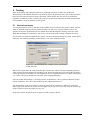
The goal of this project is to design a hardware template for the hardware connector tool. With this
template, one must be able to generate C code for the Analog devices ADSP-21992 EZ-kit Lite
evaluation board from a hardware independent 20-Sim model. The template, together with the
mentioned software tools (20-Sim, hardware connector) will be used during the so called
‘Mechatronica project’, which is a second-year project for students in Electrical Engineering at the
University of Twente.
There already exists a 20-Sim C code generation template for the ADSP-2199X family. This template
has been altered and extended to create the necessary templates for the hardware connector tool.
During the project the hardware connector also received some changes to match its goal of hardware
independence. We now have a working setup which can be used by the students to easily create a
controller in 20-Sim and run this controller at an ADSP-21992 EZ-kit Lite evaluation board.
The Hardware Connector however misses some features in the way inputs and outputs are defined.
There should be implemented some features that make it possible to bind some prerequisites to an
input or output.
To demonstrate the functional behavior of the board and the software, a demonstration setup has been
made to show (some of) the functions the board can perform, generated from a hardware independent
20-Sim model. The hardware of this demonstration setup consists of oscilloscope, wave generator and
of course the ADSP-21992 EZ-kit Lite itself.
Dutch
Het doel van dit project is het maken van een zogenaamde ‘hardware template’ voor een software tool
genaamd ‘hardware connector’. De functionaliteit van deze software in combinatie met de te maken
template moet ervoor zorgen dat er C Code gegenereerd kan worden voor een Analog devices ADSP21992 EZ-kit Lite evaluatie board vanuit een hardware onafhankelijk 20-Sim model. Deze combinatie
van software en tools (20-Sim, hardware connector en hardware template) zal gebruikt gaan worden in
het Mechatronica project in het tweede jaar van de opleiding Elektrotechniek aan de Universiteit
Twente.
Basis voor de hardware template is een bestaande C Code generatie template voor het ADSP-2199x
platform. Deze templates zijn aangepast en uitgebreid om de hardware template te creeren. Tijdens het
maken van de templates zijn er ook aanpassingen gedaan aan de hardware connector om diens doel
van hardware onafhankelijkheid te waarborgen voor meerdere platformen. Uiteindelijk is er een
werkende setup gemaakt die gebruikt kan worden door de studenten. Het is mogelijk om vanuit 20Sim een (sub)model met behulp van de hardware connector en template om te vormen tot code die
uitvoerbaar is op het Analog devices ADSP-21992 EZ-kit Lite evaluatie board.
De Hardware Connector mist ook een belangrijke optie. Het is nu niet mogelijk om eisen of
consequenties aan een input of output op te leggen, terwijl dat bijvoorbeeld in dit project zeer
wenselijk is. Deze optie zou geimplementeerd moeten worden.
Om (een deel van) alle functionaliteit van de software en hardware te demonstreren is er een
demonstratie opstelling gemaakt die aangestuurd kan worden met als basis een hardware onafhankelijk
20-Sim model. De hardware van de opstelling bestaat uit een oscilloscope, een functiegenerator en
natuurlijk het ADSP-21992 EZ-kit Lite bord zelf.
Control Engineering
ii
University of Twente
iii
Table of contents
Below is the table of contents
Introduction ......................................................................................................................................1
1.1
Assignment and background...................................................................................................1
1.2
Report outline .........................................................................................................................1
2
Hardware description .......................................................................................................................3
2.1
General Overview ...................................................................................................................3
2.2
Project specific in- & outputs .................................................................................................3
2.2.1 Digital to Analog converter ................................................................................................4
2.2.2 Analog to Digital converter ................................................................................................4
2.2.3 Digital In- & Outputs..........................................................................................................4
2.2.4 PWM Generation Unit........................................................................................................5
2.2.5 Encoder Interface................................................................................................................5
2.3
Timing.....................................................................................................................................5
3
Modeling and code generation .........................................................................................................7
3.1
20-Sim modeling.....................................................................................................................7
3.2
C-Code Generation .................................................................................................................8
4
Hardware connection......................................................................................................................11
4.1
Overview...............................................................................................................................11
4.2
XML configuration files .......................................................................................................11
4.2.1 Hardware description XML file .......................................................................................12
4.3
Code transformation .............................................................................................................14
4.4
Post processing .....................................................................................................................16
4.5
Deploy and run code .............................................................................................................17
5
Testing............................................................................................................................................19
5.1
General test setup..................................................................................................................19
5.2
Test per function ...................................................................................................................20
5.2.1 Digital to Analog converter ..............................................................................................20
5.2.2 Analog to Digital converter ..............................................................................................21
5.2.3 Digital In- & Outputs........................................................................................................23
5.2.4 PWM Generation..............................................................................................................24
6
Conclusions and Recommendations...............................................................................................25
6.1
Conclusions...........................................................................................................................25
6.2
Recommendations.................................................................................................................25
Appendix A – User manual....................................................................................................................27
Appendix B – XML Files.......................................................................................................................35
Appendix C – C source files ..................................................................................................................37
Appendix D ............................................................................................................................................39
Appendix E – Board layout and jumper settings....................................................................................41
References ..............................................................................................................................................42
1
Control Engineering
iv
University of Twente
1
1 Introduction
1.1
Assignment and background
During the so called ‘Mechatronica project’, which is a second-year project for students in Electrical
Engineering at the University of Twente, controllers are designed for dynamic systems. One of the
goals of this project is to combine knowledge of courses like “Control Engineering” and “Engineering
system dynamics”. As soon as the students have designed a controller using 20Sim software, it will be
implemented on an Analog Devices ADSP EZ-kit Lite.
To program the DSP, the C code generation functionality of 20Sim will be used, in combination with a
newly developed tool called the “Hardware Connector” by Erik Buit. There already exists a 20-Sim C
code generation template for the ADSP-2199X family; however these templates require separate dllfiles within 20Sim to run.
Objective
The objective of this BSc assignment is to design and test templates, configuration files and hardware
description files for the ADSP-21992 EZ-kit Lite to be able to generate C code from hardware
independent 20Sim models to use with the ADSP-21992 EZ-kit Lite.
1.2
Report outline
Chapter 1 is an introduction towards the rest of the report and project. After reading this chapter, the
reader should have a decent idea of what this project is about and what you can expect in the rest of
the report.
The hardware for this project consists of an Analog Devices ADSP-21992 EZ-kit Lite board. As
written before, this evaluation and development board holds an ADSP-21992 mixed signal DSP and a
number of peripherals. In chapter 2, this board and some of the used in- and output ports are discussed.
First, the general overview and functionality of the board are explained followed by a more specific
description of the in- and outputs used in this project. In section 2.3 a closer look at the timing of the
board and processor is taken.
The process of creating model code for our processor consists of three parts, all performed with
different software tools. First, there is a hardware independent model in 20-Sim. From this model Ccode is generated by means of built in 20-Sim functionality. When this is done the model code has to
be fitted for the specific hardware it will run on, in this case the Analog Devices ADSP-21992 DSP.
This task is performed by the hardware connector. After this step, the final code has to be compiled,
linked and loaded into the target. Chapter 3 deals with the first step of the process (hardware
independent part).
Chapter 4 deals with all steps needed to run the hardware independent code from the previous chapter
on the specific target hardware: the Analog Devices ADSP-21992 DSP. First I give an overview of the
process, and then I will give more detail about every step.
After all designing and coding there has to be a thorough test phase to make sure all desired
functionality of the ADSP board does work with the new code generation tool. Chapter 5 describes
these tests. First the general test setup is discussed. This describes how the tests were performed,
regardless of what test. In the sections following, all tests are discussed and plots of actual
measurements are included to verify the behavior of the system.
Finally, chapter 6 looks back on the project. It discusses the conclusions and gives some
recommendations for further research.
Control Engineering
2
University of Twente
3
2 Hardware description
The hardware for this project consists of an Analog Devices ADSP-21992 EZ-kit Lite board. This
evaluation and development board holds an ADSP-21992 mixed signal DSP and a number of
peripherals (ADSP, 2002a). In this chapter, this board and some of the used in- and output ports are
discussed. First, the general overview and functionality of the board are explained followed by a more
specific description of the in- and outputs used in this project. In the third section a closer look is taken
at the timing of the board and processor.
Figure 2-1: ADSP-21992 EZ-kit Lite board layout
2.1
General Overview
The ADSP-21992 EZ-kit Lite is an evaluation and development board (See Figure 2-1). It holds the
ADSP-21992 mixed signal DSP and a number of peripherals.
The most important features of the ADSP-21992 EZ-kit Lite board are (ADSP, 2002b):
o
o
o
o
o
o
o
o
o
o
2.2
A 16 bit, fixed point 160 MIPS DSP core. The standard operation frequency of this CPU is 16
MHz, but by means of some special software instructions the CPU can operate at a much
higher frequency: 160 MHz
32K (x24 bit) on chip program RAM and 16K (x16 bit) on chip data RAM
External memory: 64K (x16 bit) SRAM plus 512k (x8 bit) Flash memory
An 8 channel, 14 bit analog to digital (AD) converter
An 8 channel, 12 bit digital to analog (DA) converter. This DA converter is connected through
the SPI (Serial Peripheral Interface) port of the DSP
16 digital I/O pins (PF), of which 13 can be used for user-defined inputs and outputs (See
section 2.2.3)
Two three phase 16 bit PWM generation units
Two auxiliary 16-bit PWM generation units
An encoder interface
Various communication systems like RS232, USB, CAN and SPORT
Project specific in- & outputs
This section describes the in- and outputs that are used in this project. They consist of the digital to
analog converters, the analog to digital converters, the digital input and output pins, the PWM
Control Engineering
4
generation unit and the Encoder interface. In the following section, each of them is discussed in further
detail.
2.2.1 Digital to Analog converter
The signals from the digital to analog converter (DAC) are available at P5 at the left side of the board.
The DAC itself is connected to the SPI (Serial Peripheral Interface) of the ADSP-21992. The digital to
analog converter is an 8-channel, 12-bit converter. The digital data that will be output is to be loaded
into the Transmit Data Buffer Register of the SPI, which then will be converted into analog signal by
the DAC.
To put an analog signal on the DAC’s they have to be activated by setting two flags to a ‘high’ level.
These are PF2 and PF3 (the first is used to activate the DAC’s while the latter is used to update the
DAC registers). Unlike the analog to digital converters the output of the DAC’s is asymmetric (from 0
to +2 Volts) and cannot be altered.
2.2.2 Analog to Digital converter
The input pins for the analog to converter (ADC) are available at P4 at the left side of the board. The
ADC itself consists of an 8-channel, 14 bit pipeline flash ADC with dual channel simultaneous
sampling capability. This means that two channels are subsequently sampled simultaneously: channel
0 & 4 together, then 1 & 5 together, then 2 & 6 together and ending with 3 & 7 together.
The AD-conversion can be triggered in 4 different ways:
• By generating interrupts with the Three-Phase PWM unit (resembling an internal clock).
• By generating interrupts with the Auxiliary PWM unit (resembling an internal clock).
• By external triggering (rising edge on CONVST pin) (resembling an external clock).
• By writing to the SOFTCONVST register of the AD-converter (user command).
The ADC system can be programmed to operate at a clock rate that is programmable from the
peripheral clock ÷ 4 to the peripheral clock ÷ 30, to a maximum of 20 MHz (at 160MHz Core clock
rate). See also section 2.3.
When triggered, all of the 8 input channels are sampled and converted. All 8 inputs converted in
approximately 725 ns (at 20 MSPS), so a maximum sample frequency slightly over of 1.3 MHz on
each channel is achievable.
When finished converting, the data is put into data-registers. The status register contains 4 ‘finished
converting’ flags. Each flag stands for a combination of 2 channels (0 & 4, 1& 5, etc.). When the input
signals are successfully converted and put into the data registers (ADC_DATA#, with # ranging 0–7)
these status flags are made high to indicate a successful conversion.
The input range of the ADC is always 2Vpp and default symmetric: from -1 to +1 Volt. If needed, an
external reference voltage can be applied to the processor to indicate the maximum voltage input.
2.2.3 Digital In- & Outputs
The digital in- outputs are available at P8, at the top of the board. They are numbered PF0 to PF15
(Programmable Flag). However, not all pins can be used for user defined inputs or outputs. PF2 and
PF3 are used to operate the DAC’s whilst PF15 is used for PWM generation (See section 2.2.4). This
leaves 13 pins for user defined inputs or outputs.
The FIO module is a generic parallel I/O interface that supports sixteen bidirectional multifunction
flags or general-purpose digital I/O signals (PF15–PF0). All sixteen FLAG bits can be individually
configured as an input or output based on the content of the direction (DIR) register, and can also be
used as an interrupt source for one of two FIO interrupts. When configured as input, the input signal
University of Twente
5
can be programmed to set the FLAG on either a level (level sensitive input/interrupt) or an edge (edge
sensitive input/interrupt).
2.2.4 PWM Generation Unit
The ADSP-21992 integrates a 2-channel, 16-bit, auxiliary PWM output unit that can be programmed
with variable frequency, variable duty cycle values and may operate in two different modes,
independent mode or offset mode.
In independent mode, the two auxiliary PWM generators are completely independent and separate
switching frequencies and duty cycles may be programmed for each auxiliary PWM output.
In offset mode the switching frequency of the two signals on the AUX0 and AUX1 pins is identical.
Bit 4 of the AUXCTRL register places the auxiliary PWM channel pair in independent or offset mode.
There currently only works one PWM generator. The PWM output block of this generator is
connected via the AUX0 and DGND pins on P10 at the bottom of the board. The direction pin for the
PWM is connected via PF15, one of the programmable flags on P8 at the top of the board.
2.2.5 Encoder Interface
The ADSP-21992 incorporates an encoder interface block to incremental shaft encoders that are often
used for position feedback in motion control systems.
The encoder interface unit (EIU) includes a 32-bit quadrature up/down counter, programmable input
noise filtering of the encoder input signals and the zero markers, and has four dedicated chip pins.
The quadrature encoder signals are applied at the EIA and EIB pins. Alternatively, a frequency and
direction set of inputs may be applied to the EIA and EIB pins. In addition, two north marker/strobe
inputs are provided on pins EIZ and EIS. These inputs may be used to latch the contents of the encoder
quadrature counter into dedicated registers, EIZLATCH and EISLATCH, on the occurrence of
external events at the EIZ and EIS pins. These events may be programmed to be either rising edge
only (latch event) or rising edge if the encoder is moving in the forward direction and falling edge if
the encoder is moving in the reverse direction (software latched north marker functionality).
The encoder interface unit operates at a clock frequency equal to the peripheral clock rate. The
encoder interface unit operates correctly with encoder signals at frequencies of up to 13.25 MHz, at
the 80 MHz peripheral clock rate, corresponding to a maximum quadrature frequency of 53 MHz
(assuming an ideal quadrature relationship between the input EIA and EIB signals).
The encoder interface unit of the ADSP-21992 contains a 16-bit loop timer that consists of a timer
register, period register and scale register so that it can be programmed to time out and reload at
appropriate intervals.
2.3
Timing
The ADSP-21992 can be clocked by a crystal oscillator or a buffered, shaped clock derived from an
external clock oscillator.
If a crystal oscillator is used, the crystal should be connected across the CLKIN and XTAL pins. If a
buffered, shaped clock is used, this external clock connects to the CLKIN pin. CLKIN input cannot be
halted, changed, or operated below the specified frequency during normal operation. When an external
clock is used, the XTAL input must be left unconnected. The DSP provides a user programmable 1 to
32x multiplication of the input clock, including some fractional values. Together, they form support
for 128 external to internal (DSP core) clock ratios.
Control Engineering
6
The BYPASS pin, and MSEL6–0 and DF bits, in the PLL configuration register, decide the PLL
multiplication factor at reset. At run time, the multiplication factor can be controlled in software. To
support input clocks greater that 100 MHz, the PLL uses an additional bit (DF). If the input clock is
greater than 100 MHz, DF must be set. If the input clock is less than 100 MHz, DF must be cleared.
For clock multiplier settings, see the ADSP-2199x DSP Hardware Reference Manual. The peripheral
clock is supplied to the CLKOUT pin. All on-chip peripherals for the ADSP-21992 operate at the rate set
by the peripheral clock. The peripheral clock (HCLK) is either equal to the core clock rate (CCLK) or half
the core clock rate. This selection is controlled by the IOSEL bit in the PLLCTL register. The maximum
core clock rate is 160 MHz, and thus the maximum peripheral clock rate is 80 MHz.
When resetting the ADSP-21992, it uses an integrated power-on reset (POR) circuit to guide its
booting. This POR circuit provides an output reset signal from the ADSP-21992 on power-up and if
the power supply voltage falls below the threshold level. The ADSP-21992 may be reset from an
external source using the RESET signal, or alternatively, the internal power-on reset circuit may be used
by connecting the POR pin to the RESET pin. During power-up the RESET line must be activated for long
enough to allow the DSP core’s internal clock to stabilize. The power-up sequence is completed when
the crystal oscillator is stabilized after a valid VDD is applied to the processor and when the internal
phase-locked loop (PLL) is locked onto the specific crystal frequency. Various manuals suggest
waiting a minimum of 512 cycles to ensure that the PLL has locked.
As told before, the ADSP-21992 provides a user-programmable multiplication of the input clock. The
pin, MSEL6-0, and DF bits in the PLL configuration register, specify the PLL multiplication
factor at reset. When jumper JP12 is closed, BYPASS mode is selected. This means in that situation
the PLL will be bypassed.
BYPASS
University of Twente
7
3 Modeling and code generation
The process of creating model code for our processor consists of three parts, all performed with
different software tools. First, there is a hardware independent model in 20-Sim. From this model Ccode is generated by means of built in 20-Sim functionality. When this is done the model code has to
be fitted for the specific hardware it will run on, in this case the Analog Devices ADSP-21992 DSP.
This task is performed by the hardware connector. After this step, the final code has to be compiled,
linked and loaded into the target. This chapter deals with the first step of the process (hardware
independent part) and the next chapter (chapter 4) deals with the last 2 steps of the process.
Figure 3-1: Example model for use with ADSP EZ-Kit Lite
3.1
20-Sim modeling
The basis starting point for every controller implemented by means of 20-Sim is a 20-Sim model. This
model must at least consist of a model of the plant which will be controlled and the controller itself.
See Figure 3-1; in this example, the code will be generated from all operations inside the block
‘Controller’.
When designing models with tools like 20Sim the user wants to abstract the model from the real
implementation. The controller model must represent the plant, but should preferably not be dependent
on any hardware implementations that do not belong to the plant. A plant that takes an analogue signal
as input, for example, is not depending on the way this signal is generated.
The user must be able to specify the hardware in one of the last stages of designing. At the model
verification stage, it should be able to verify behavior of a model, regardless of the hardware it will be
implemented in ultimately. Then, in principle, any hardware can now be used to generate the analogue
signal from the example.
20sim has a feature to use DLL’s (Dynamic Link Libraries) to “emulate” special behavior in models.
When C code is generated, the DLL function call will end up in the code with the connected signals as
parameter vectors. What was done is that function calls with the same name as the DLL where added
to the source by means of libraries. The linker connected the function calls to the final executable and
made hardware access possible.
A disadvantage of this approach is that in 20sim an empty DLL must be made to allow simulation.
The DLL is not a real calculation but a ‘trick’ to use hardware after the code is generated. Another
disadvantage is that the naming of the function calls gets blurred. The templates needed to cope with
the DLL function calls, and initialization had to be performed in the template. For every piece of
hardware a different template is needed. If more than one device is used the number of templates will
grow exponentially to allow the user to use any kind of hardware configuration. Not taken is into
account is the fact that hardware may need to initialized differently in some situations. For example an
analogue input or output card may have a range of 0..10V or 10..20mA. If these options must be
selectable by the user even more templates need to be created. For all these reasons, it is preferable to
be able to use generalized 20Sim models in order to overcome the problem of multiple templates and
get rid of the DLL ‘trick’.
Control Engineering
8
Figure 3-2a: From old Code generation process …
Figure 3-3b: … to new Code generation process
To illustrate what changes will be made in the process, take a look at Figure 3-2a (Mocking, 2002)and
Figure 3-3b.
One can see that all hardware dependent parts are “stripped” from the 20Sim code generation process.
The real hardware calls will be inserted into the code after 20Sim has finished its job. One small issue
in this new situation is the fact that still there is a hardware dependent part of the C code generation
process which will be handled by 20Sim. These are the C source files, which will be modified by
20Sim (replacing the tags with corresponding values). However, these files have nothing to do with
the modeling part of a controller design process, and therefore have no influence on our desired
hardware independent modeling.
3.2
C-Code Generation
The newest versions of 20-Sim (version 3.1 or later) include a code generation tool, which can be used
to generate C-code for a various number of targets, in order to let these targets perform certain tasks
(Groothuis, 2001). The code generation tool can be accessed via the 20-Sim simulator window. Ccode generation can be accessed via the menu-item “Tools” (20Sim version < 3.4) or “Tools” - “Real
Time Toolbox” (20Sim 3.4 or later) in the simulator.
When having created a model or a system consisting of one or more submodels, the user can choose to
simulate his creation. When the model is processed, the code generation tool becomes available in the
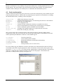
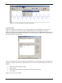
Tools menu of the 20-Sim simulator. The user can choose between various targets (Figure 3-4).
University of Twente
9
Figure 3-4: C-Code generation dialog
These targets are specified in a target configuration file called Targets.ini. When choosing a target
which supports submodel code generation, the user can also choose a submodel. After choosing a
target, submodel and output directory, pressing “OK” will initiate the real code generation process.
This process consists of several subsequent steps, visualized in Figure 3-2.
When necessary, a pre-processor can be started, which can process the unfinished template files
beforehand.
The template files contain tags. When code-processing, these tags are replaced by 20-Sim states, rates,
parameters etc. Finally, the finished template files are copied to the output directory that was specified
in the code generation dialog, Figure 3-4. The template files in which the tokens are filled in, are
specified in Targets.ini by the “templateFiles=” command. These files are put in a subdirectory in the
20-Sim Ccode directory. The template files will be taken from this subdirectory, processed as
described in the previous lines, and then put into the output directory.
In the output directory a post-processor can be started, which will process the template files further.
For example a compiler, a linker and a loader can be started for running the program on the target that
has been chosen in the code generation dialog window.
Control Engineering
10
University of Twente
11
4 Hardware connection
The step from hardware independent code towards code that will run on a specific hardware platform
is performed by the Hardware Connector (Buit, 2005). This is a tool written by Erik Buit for his MSc
thesis. This chapter deals with all steps needed to run the hardware independent code from the
previous chapter on the specific target hardware: the Analog Devices ADSP-21992 DSP. First an
overview of the process will be given, followed by a more detailed explanation about every step.
4.1
Overview
After code has been generated from the model in 20Sim, this code has to be made suitable to run at the
specific target hardware (see Figure 4-1).
Figure 4-1: Transformation process
A tool called the ‘hardware connector’ is used for this purpose. All configuration data for this tool is
stored in XML files. The structure and contents of these files are discussed in section 4.2. The
combination of 20Sim generated c-code, the hardware connector and the XML files leaves C-code
files which can be compiled by the ADSP compilers. This process is discussed in sections 0 and 4.4.
The ADSP compiler takes all source files and produces an executable which needs to be transferred to
the ADSP EZ-kit Lite. This is done by means of the Crosscore Visual DSP++ software. Also the task
of starting the control software on the target processor is taken care of by this software. The process is
discussed in section 4.5.
4.2
XML configuration files
Extensible Markup Language (XML) is a document syntax developed by the World Wide Web
Consortium (W3C) (W3C, 2004) . XML is a simple, very flexible text format which was originally
designed to meet the challenges of large-scale electronic publishing; XML is also playing an
increasingly important role in the exchange of a wide variety of data on the Web and elsewhere.
XML documents are made up of storage units called entities or elements, which contain either parsed
or unparsed data. XML also provides a mechanism to impose constraints on the storage layout and
logical structure. The configuration files of the hardware connector are written in this text format. For
a quick impression of a XML layout, see Listing 4-1 (Pieces of the file have been left out and replaced
by “...”).
<ADSP21992>
<Parameters Kind="Analog Devices ADSP" DeviceID="0" Config="" Includes="" ... >
<Input>
<getADInput Nr="8" Name="AD input" />
<ENC_Handler Nr="1" Name="Encoder input" />
<getDInBit Nr="15" Name="Digital input" />
</Input>
<Output>
<AUXPWM_write Nr="1" Name="PWM Output" />
<setDOutBit Nr="15" Name="Digital Output" />
...
</Output>
...
</Parameters>
...
</ADSP21992>
Listing 4-1: Part of XML file as an example
Control Engineering
12
An XML file always has one root element, in this example “ADSP21992”. Every element can have
one or more children (which can have children of their own, and so forth). Also, a node can have
attributes. In the example, the node ADSP21992 has a child “Parameters”, which has attributes
“Kind”, “DeviceID”, “Config”, and etcetera. “Parameters” has two children of his own: “Input” and
“Output”, which have their own attributes. An element is described by a tag. A tag is a word
surrounded by “<” and “>”. An XML element must always be closed by a “/”. This slash can be either
in the same tag, or in a closing tag. To illustrate this, Listing 4-2 shows two pieces of code which have
the same meaning in XML. Of course, in the first code example the “Output” node can have children,
the second it cannot.
<Output argument1=“1” argument2=“2”>
<Output argument1=“1” argument2=“2” />
</Output>
Listing 4-2: Two different XML texts with the same meaning
The hardware connector uses two XML files ADSP21992.xml and CCE.xml (for a full listing of the
content of these files, see appendix B).
The ADSP21992.xml file contains the hardware description and functions to get the functions of the
ADSP processor to work. See section 4.2.1 for a complete description of the ADSP21992.xml file.
The CCE.xml file contains information for the hardware connector to work. It contains some variables
which will be changed by 20Sim in the code generation process, for instance %GENERATION_DIR% and
%NUMBER_VARIABLES%. These variables will be replaced into their corresponding values by 20Sim, and
are required by the hardware connector to work properly.
4.2.1 Hardware description XML file
The ADSP21992.xml file contains the hardware descriptions and functions. Roughly said, the file can
be split into 4 pieces: Descriptions for input and output, Startup procedures, Shutdown procedures and
Transfer functions. All of these pieces are discussed in the next sections.
4.2.1.1 Descriptions for input and output
The descriptions for input and output (caught in the XML element “Parameters”) describe which input
ports and output ports are available at the target. In the XML file, the element name is the name of the
function to call (see section 4.2.1.4) and is has two arguments: “Nr” and “Name”. The first argument
sets the number of available ports for each type of input or output. The argument “Name” is used to
give the port a ‘friendly’ name. However, this argument is not used anywhere yet. Listing 4-3 shows
one example of an input port.
<Parameters Kind="Analog Devices ADSP" ...>
<Input>
<getADInput Nr="8" Name="AD input" />
Listing 4-3: Part of ADSP21992.xml file
This port is an input and will be called “getADInput”. “Nr” shows that we have eight of these ports,
which will be numbered 0..7 automatically.
4.2.1.2 Startup procedures
This section deals with the startup of the target platform. The contents of this procedure are in the
XML element “Startup”. The first argument, “sequence” denotes the sequence of startup. The value of
this argument can be either “OI” of “IO”, the first meaning the device should first be opened and then
initialized. The latter means that these actions should be taken in reverse order: first initialized and
then opened. In the case of the ADSP21992 this order does not matter because the initialization part
University of Twente
13
only exists of declaration of variables. These variables are not used for the initializing the target, so it
doesn’t matter if they are declared before or after initializing the target.
One may have briefly noticed the startup functions: “Open” and “Initialize”. These functions are also
defined in the XML element “Startup” as children of this element. “Open” takes one argument,
“function”, and places this code where it opens the device. This function is already available in the
ADSP21992.c source code as “ADSP21992_Initialize”, so only the function name is given as
argument:
<Open function="ADSP21992_Initialize();" />
Listing 4-4: Open function
The initialization part of the XML files only consists of declaration of some variables. This is not
discussed here. The relevant parts of these declarations are discussed in section 4.2.1.4.
4.2.1.3 Shutdown procedures
This deals with the shutdown of the target. The contents of this procedure are in the XML element
“Shutdown”. The first argument, “sequence” is similar to the same argument of “Startup”: it denotes
the sequence of shutdown. This time, the combination of the letters “R” and “C” denotes the shutdown
sequence. “R” means “Reset”, and “C” means “Close”. Again, these functions are defined in children
of the “Shutdown” element: “Close” and “Reset”. In the case of the ADSP21992 target, there exists a
function “ADSP21992_Termintate” in the ADSP21992.c file. Similar to the “Open” function, this
function name is given as argument to “function”. The ADSP21992 target has no need for specific
reset operations, to this XML element is left empty (and therefore the value of sequence may be “RC”
or “CR”, since the order doesn’t matter).
4.2.1.4 Transfer functions
The transfer functions are the functions that really “do the job”. These functions write to the outputs
and read from the inputs. This part of the XML description file is in Listing 4-5.
<Transfer>
<Read scale="" function="ADSP21992_%type%%channel%(&dummyin, 1, &%var%, 1,
xx_major);" />
<Write scale="" function="ADSP21992_%type%%channel%(&%var%, 1, &dummyout, 1,
xx_major);" />
</Transfer>
Listing 4-5: Part from ADSP21992.xml
The “Read” and “Write” elements describe the inputs and outputs, respectively. As you may notice,
there are some tags (the text between %-signs) in the function descriptions. All functions, regardless of
their type, will be called by these functions. The replacement of the tags by useful information decides
which precise function is called. During the hardware connection process, several replacements are
made:
• %type% will be replaced by the type of the input / output (these types are defined in the
descriptions for input and output, see section 4.2.1.1)
• %channel% will be replaced by the number of the channel. This channel number depends on
the channel the user selects during the hardware connection process.
• %var% will be replaced by the actual variable name in the source code generated by 20Sim.
All functions that read from an input or write to an output in the ADSP21992.c file have the same
prototype (“???” denoting the type like “getADInput”)
ADSP21992_??? (double *inarr, int inputs, double *outarr, int outputs, int major)
Listing 4-6: Function prototype in ADSP21992.c
Control Engineering
14
Because read function is very unlikely to be given the double inarr, a dummy double has been created
for this purpose. The same holds for the write functions and the outarr double. The dummy double
variables (called “dummyin” and “dummyout”) are defined in the initialization process.
4.3
Code transformation
After the 20Sim code generation process, there are several files in the directory where 20Sim was told
to put the generated code in. All files that are needed for proper operation are listed below (excluding
the standard 20Sim files), including a short description.
2199x_ivt.dsp
ADSP21992.c
ADSP21992.h
CCE.xml
compile.bat
Main.h
pll.dsp
SPI_dac_21992.dsp SPI_dac.h
-
ADSP 2199x interrupt vector table
Contains all functions necessary for interfacing the software to the hardware
Header file for ADSP21992.c
CCE configuration file
Contains all DOS commands to build an executable from sources
File for setting hardware parameters like clock frequency en multiplier
Used for setting the speed to 160MHz instead of 16MHz
Assembly file containing functions to operate the DA-converters
Header file for SPI_dac_21992.dsp
Still, several of these files contain tags that are not replaced right now. Because 20Sim did not
recognize these tags, they were left in the code. These tags are dependent on the hardware used, and
will be replaced by the Hardware Connector. All available tags are
%IO_INCLUDES%
%IO_GLOBALS%
%IO_INITIALIZE%
%IO_READ_ROUTINE%
%IO_WRITE_ROUTINE%
%IO_CLOSE%
-
Used for include files
Used to define global variables
Initialization functions (initialization and opening)
Read routines
Write routines
Closing routines (reset as well as close)
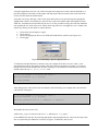
For some of these tags, the Hardware Connector still needs more information from the user before it
can actually replace these tags by appropriate values. For instance to know what code to place at the
spot where %IO_READ_ROUTINE% is, it needs to know what hardware it should read from. The hardware
connector is equipped with a hardware channel connector for this purpose. After 20Sim code
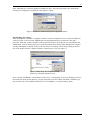
generation, a dialog window pops up (see Figure 4-2).
Figure 4-2: Hardware Connector main dialog
University of Twente
15
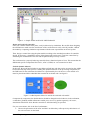
Using this application, the user can connect all input and output ports of the selected submodel to a
physical peripheral. The names of the inputs and output ports that are listed in the lower half of the
screen are taken from the 20Sim model.
First, add a device by choosing “Add” in the upper half of the screen and selecting the appropriate
ADSP21992.xml file. The Hardware Connector now reads all available input and outputs from this
XML file, and makes them selectable for the user. It is now possible to map ports from the submodel
onto peripherals. For each of the ports, follow these steps (the user can toggle the view of inputs and
outputs by clicking on the inputs or outputs button).
•
•
•
•
Click on the desired input or output
Click connect
Choose the appropriate Device, IO Kind and Channel from each list (See Figure 4-3)
Click Apply
Figure 4-3: Connecting a port to a physical channel
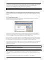
To illustrate what the Hardware Connector does, the example from above is used. After C code
generation from 20Sim, part of the xxmain.c file looks like the part shown in Listing 4-7. From the
transfer functions in the ADSP21992.xml file (Listing 4-5), the Hardware Connector knows what it
should replace the tag %IO_WRITE_ROUTINE% with.
/* call the submodel to calculate the output */
XXCalculateSubmodel (u, y, xx_time);
%IO_WRITE_ROUTINE%
Listing 4-7: Part of xxmain.c
After filling in the values selected in the channel connection dialog, the example above becomes the
code listed in Listing 4-8.
/* call the submodel to calculate the output */
XXCalculateSubmodel (u, y, xx_time);
ADSP21992_setDAOutput0(&u[2], 1, &dummyout, 1, xx_major);
Listing 4-8: Part of xxmain.c after HWC
Remember, the line used to read
ADSP21992_%type%%channel%(&%var%, 1, &dummyout, 1, xx_major)
in the ADSP21992.xml file. By selecting appropriate output peripherals, the values for the tags in this
line are replaced by the Hardware Connector (%type%, %channel% and %var%).
Control Engineering
16
4.4
Post processing
Once all files have been altered, it is time to create an executable from them. This process is taken care
of by a MS-DOS batch file run from the compiler assistant. The MS-DOS file, called ‘compile.bat’,
contains all DOS commands needed to call all tools that perform the post processing (ADSP, 2002c).
For a full review of the compile.bat file, please take a look at appendix D.
In Figure 4-4, the relation between the different file types in the Visual DSP++ tool chain is shown.
Figure 4-4: From source to executable
First of all, a library file is built. Because the available memory space on the ADSP board is limited,
the created executable must be as small as possible. By building a library file from which the unused
functions in the source code are excluded, unused code is excluded (which will make the code
smaller). During compile time, the ADSP compiler is capable of checking for functions that are used
and building a library file containing only those used functions. The way to do this is shown in Listing
4-9; all files that may have unused code are given to the compiler, which then also optimizes for
minimum size (the –Os flag). The file “libccode.dlb” is built as a result of issuing this command.
cc219x -Os xxmodel.c xxfuncs.c xxsubmod.c xxinteg.c adsp21992.c spi_dac_21992.dsp
timer.c -build-lib -o libccode.dlb
Listing 4-9: Building library file
Next, the assembly files have to be assembled into an object file. This is done by issuing the
commands in Listing 4-10. In this listing it is specified that we will be running the file on an “ADSP21992” processor by adding the –proc command-line option.
easm219x -proc ADSP-21992 -o 2199x_ivt.doj 2199x_ivt.dsp
easm219x -proc ADSP-21992 -o pll.doj pll.dsp
Listing 4-10: Assembling
Also, the remaining C code has to me assembled into an object file, see Listing 4-11. Again,
optimizations for size (-Os) and an ADSP-21992 processor (-proc ADSP-21992) are performed and
this time build (-o) a file called “xxmain.doj”.
cc219x -Os -c xxmain.c -proc ADSP-21992 -o xxmain.doj
Listing 4-11: Building ADSP21992 object file
University of Twente
17
As a final step, all created objects have to be linked together into one executable file. The linker takes
all object files (.doj) and the library file (.dlb) and links them into the executable file called
“runme.dxe”. The command line to achieve this is shown in Listing 4-12.
cc219x -Os 2199x_ivt.doj pll.doj xxmain.doj -lccode -T ADSP-21992.ldf –proc
ADSP-21992 -o runme.dxe
Listing 4-12: Linking and building the final runme.dxe
An DSP executable file is now created which can be run at the ADSP-21992 EZ-kit Lite. As said
before, all commands above are wrapped together into one batch file which is started by the compiler
assistant. This means that the user will not have to have any concerns about compiling the generated
sources.
4.5
Deploy and run code
The process of the previous section is performed by a MS-DOS batch file which is run after the
hardware connector has finished. See Figure 4-5.
Figure 4-5: Finished compiler
When done, the compiler assistant should say it finished without any error. Now, the generated
runme.dxe executable file has to be transferred into the ADSP21992 EZ-kit Lite. For this task, the
Crosscore VisualDSP++ Integrated Development Environment (IDDE) is used.
In the VisualDSP++ environment, choose the ‘Load program’ option from the File menu. In the next
dialog box, specify the runme.dxe file that will be loaded. When the upload is finished, Visual DSP++
may run the code on the ADSP board (Press F5 in VisualDSP++, or choose Debug - Run).
It is possible to even decrease a couple of mouse clicks here by automating the process of loading and
running the dxe file. For this, a tcl file will have to be created, which can be loaded by the idde.
Put these 2 lines in a file:
dspload runme.dxe
dsprun
and enter this command at the command prompt:
idde –f runandload.tcl
where “runandload.tcl” is the filename of the created tcl file. When running the target this way,
"Switching off" of the ADSP-21992 EZ-kit Lite board is in this case performed by hitting the ‘reset’
switch.
For a tutorial / user manual of the complete process, see Appendix A – User manual.
Control Engineering
18
University of Twente
19
5 Testing
After all designing and coding there has to be a thorough test phase to make sure all desired
functionality of the ADSP board does work with the new code generation tool. This chapter describes
these tests. First the general test setup is discussed. This describes how the tests were performed,
regardless of what test. In the second section, all tests are discussed and plots of actual measurements
are included to verify the behavior of the system.
5.1
General test setup
To verify the behavior of every function of the ADSP board, several tests have been created. Also the
order in which the tests have been performed makes sure that every separate function works. For
instance the first test performed is the test which shows that the Digital to Analog converters work.
With that knowledge we performed a test to prove the working of the Analog to Digital converters.
Several times we needed an input for the system. For this a function generator was used. Unless noted
otherwise, this function generator produced a 2Vpp sine wave without an offset.
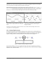
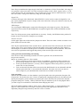
Figure 5-1: All simulations run at 100Hz, unless specifically
noted otherwise
When code is generated, the code generation process takes the ‘Discrete System sampling frequency’
value from the 20-Sim simulator and produces code which will make the system run at this frequency.
Unless specifically noted otherwise, all simulations run at a sampling frequency of 100Hz (See Figure
5-1), so the real system should also run at this same sampling frequency.
Once the model functionality is verified by means of simulations, code is generated from this model
and its simulation. This code is then loaded into the ADSP target and run.
The functionality of the real system is verified by means of an oscilloscope. Whenever needed, an
input signal is provided to the system and its output is observed. From every test setup an oscilloscope
image is made to show the output of every test.
In the next section all specific tests are discussed and results are shown.
Control Engineering
20
5.2
Test per function
5.2.1 Digital to Analog converter
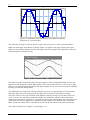
The model for testing the Digital to Analog converters is shown in Figure 5-2.
Figure 5-2: Model of Digital to Analog test setup
To make sure the all outputs work as we desire, first waveforms will be generated inside the ADSP
which will be transferred to the Digital to Analog converters (so no inputs are applied). All waveforms
(sine, triangle and square) are generated inside the ADSP and each of them is connected to an output.
To make sure all waveforms use the full voltage-swing available at the output, some wave generator
outputs are level shifted by -1V to make sure their output is between -1 and +1V.
This setup is run in the 20-Sim simulator. The results of this simulation are in Figure 5-3. The same
simulation was performed with a lower sampling frequency to observe the behavior of the system in
that situation (See Figure 5-4).
model
model
SignalMonitor1
2
SignalMonitor1
2
1
1
0
0
-1
-1
-2
-2
SignalMonitor2
2
SignalMonitor2
2
1
1
0
0
-1
-1
-2
-2
1
1
SignalMonitor3
SignalMonitor3
0.5
0.5
0
0
-0.5
-0.5
-1
0
1
2
3
4
5
time {s}
6
7
8
9
Figure 5-3: Simulation of the Digital to Analog
test model
10
-1
0
1
2
3
4
5
time {s}
6
7
8
9
10
Figure 5-4: Same simulation at a lower, 10 Hz,
sampling frequency
As you can see, both simulations show exactly what one would expect. Code is generated from both
situations and run on the ADSP board. The result of the first situation is shown in Figure 5-5, the
result of the second situation is shown in Figure 5-6. In the first situation you can clearly recognize
both shaped that are displayed (unfortunately, the oscilloscope is only capable of showing two
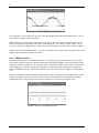
channels at the same time). To verify the actual sampling frequency we take a look at the second
situation. In this case, the sampling frequency is should be 10Hz. To verify this, a closer look is taken
at the triangular waveform. Using built-in functionality of the oscilloscope, we place 4 so-called
‘cursors’ over the signal. These cursors can be seen in Figure 5-6 as the 2 horizontal and 2 vertical
University of Twente
21
dotted lines. Two vertical cursors are placed over one ‘period’ of sampling, while the two horizontal
cursors are placed over the upper and lower boundary of the signal.
Below the signal, the interesting values of these cursors can be seen. First, the 1/ΔX = 10.000Hz
shows that the sampling frequency indeed matches the 10Hz from the 20-Sim simulator. Secondly, the
ΔY(2) = 2.000V shows that the signal indeed uses the full available spectrum of 2Vpp. These 2Volts
are from 0 to +2Volts (note the tiny GND sign at the left side of the oscilloscope image).
Figure 5-5: Result of the Digital to Analog test
system with two outputs plotted (sine- and square
wave)
Figure 5-6: Result of the same system running at a
10 Hz sampling frequency and showing the
triangle waveform
The behavior of the Digital to Analog converters is now verified. This knowledge will be used to
verify behavior of other peripherals.
5.2.2 Analog to Digital converter
The functional verification of the Digital to Analog converters will be used to verify the behavior of
the Analog to Digital converters. A signal, generated by an external wave generator, will be applied to
one of the Analog to Digital converters and directly made available on the output by means of a
Digital to Analog converter. The 20-Sim model for this test setup is shown in Figure 5-7.
Figure 5-7: Model of Analog to Digital test model
In the 20-Sim simulator, a sine wave is applied at the input. This input is sampled by the Analog to
Digital converter. In Figure 5-8, this sampled sine is plotted three times (with three different sampling
frequencies; 1Hz, 10Hz and 100Hz).
Control Engineering
22
model
1
SampledSine
0.5
0
-0.5
-1
0
1
2
3
4
5
time {s}
6
7
8
9
10
Figure 5-8: Simulation of AD test model at three different sampling
frequencies (1, 10 and 100 Hz)
The simulation of Figure 5-8 shows what we expect from out system, so code is generated from it.
When run at the target, the behavior looks like Figure 5-9. Signal 1 (the upper signal) is the signal
applied to the Analog to Digital converter and signal 2 (the lower signal) is the signal that is retrieved
from the Digital to Analog converter.
Figure 5-9: Result of the Analog to Digital test system
The behavior of this system looks good. The input signal is clearly sampled and output, and also the
frequencies of both signals is equal. When taking a close look at both sine waves, one can see a slight
latency of the sampled signal compared to the original signal. This is not an error and can be explained
by taking a closer look at this latency.
The ADSP processor samples the Analog to Digital converters at a specified rate (set in the 20-Sim
simulator), does some processing and puts the output in the registers of the Digital to Analog
converters. However, the real activation of the Digital to Analog converters is only done in the next
cycle. So in our case, this latency should be roughly one sample time and thus can be adjusted by
changing the parameters in 20-Sim. To verify this conclusion, two measurements have been taken: one
(same) sine wave will be applied to the ADSP board and sampled at two different rates: 100Hz and
1kHz. In both cases there will be zoomed into a portion of the sine which clearly shows the latency.
The results of this test are in Figure 5-10 and Figure 5-11.
University of Twente
23
Figure 5-10: Latency of sine applied to the system
at 100 Hz sampling frequency
Figure 5-11: Latency of same system at 1 kHz
sampling frequency
These measurements support the conclusion that the latency depends on the sampling frequency set in
the 20-Sim simulator. One can clearly see that in the second case, with the higher sampling frequency,
has a much lower latency. Also in the first case the latency seems to be (roughly) equal to the
sampling time. Further measurements into this matter support this conclusion and have shown that the
latency is exactly equal to the sampling time.
Supported by all measurements above, one can safely draw the conclusion that code generation for the
Analog to Digital converters does work.
5.2.3 Digital In- & Outputs
The functional behavior of the Digital Inputs and Digital Outputs is verified by using the same model
as was used for the Analog to Digital converters. This can be done because essentially both peripherals
‘act’ quite the same: a signal, generated by an external wave generator, will be applied to one of the
Digital Inputs and directly made available on the output by means of a Digital Output. The 20-Sim
model for this test setup is shown in Figure 5-12.
Figure 5-12: Model for Digital Input- and Output test
Because a simulation of this model has been performed when verifying the functional behavior of the
Analog to Digital converters (see section 5.2.2), that model simulation is not repeated here. The only
difference between this and the previous run is the number of bits in the Analog to Digital converter.
This time, it is 1 bit; however, this does not make a significant difference because the model is verified
by applying an input and checking the output.
When running the newly created code on the ADSP, we can observe this behavior (Figure 5-13). The
sine is provided to the system, and the square wave is the output.
Control Engineering
24
Figure 5-13: Result of Digital Input and Output test
This setup gives us two answers at one run: “does the Digital Input and Digital Output work”, and “at
what value is an Input considered ‘high’”?
Both questions are answered by taking a look at the figure. Because of the straight-forward way the
input is put through to the output, any input considered ‘high’, will result in a ‘high’ output. As you
can see, an input value higher than ≈ 1,438 Volt is considered high (note the cursors and their values).
Supported by the measurements above, one can safely draw the conclusion that code generation for the
Digital Inputs and Digital Outputs does work.
5.2.4 PWM Generation
The functional behavior of the PWM Generator is verified by using the same model as was used for
the Analog to Digital converters and the Digital Inputs and Digital Outputs. This can be done because
essentially all these peripherals ‘act’ quite the same: a signal, generated by an external wave generator,
will be applied to one of the Analog to Digital Inputs and directly made available on the output by
means of a PWM Generator. The 20-Sim model for this test setup is shown in Figure 5-7 and Figure
5-12.
Because a simulation of this model has been performed when verifying the functional behavior of the
Analog to Digital converters (see section 5.2.2), that model simulation is not repeated here. When
running the newly created code on the ADSP, this behavior can be observed (Figure 5-14).
Figure 5-14: Result of PWM generation
University of Twente
25
6 Conclusions and Recommendations
6.1
Conclusions
A working setup of hardware independent 20Sim modeling, the Hardware Connector and the ADSP21992 EZ-kit Lite has been created. The setup of various software tools and files can be successfully
used to program an Analog Devices ADSP-21992 chip with controller software created from a
hardware independent 20Sim model.
Tests have shown that the template’s functionality is good. All functions that are supported are Analog
to Digital conversion, Digital to Analog conversion, Digital inputs, Digital Outputs, Pulse Width
Modulation generator and an Encoder interface. Measurements on all these functions prove the correct
functioning of these devices.
During the design process of template files for the Hardware Connector, several changes have been
proposed to Erik Buit. The current version of the Hardware Connector works well, but some features
and usability issues exist in this software and the way templates are handled.
6.2
Recommendations
Templates
There are many possibilities and hardware peripherals that are not yet available via the templates that
were created. In various chapters the (extra) PWM controllers have been mentioned as an example of
this, but also memory expansion slots are not used with this template. Maybe it even turns out to be
possible to use the various communication systems.
Hardware Connector
The hardware connector uses a XML hardware configuration file to know the abilities of the hardware
it modifies the generated code for. A missing feature is in the way inputs and outputs are defined. It is
currently not possible to bind some prerequisites to an input or output. An example from this project is
the usability of the digital inputs and outputs. They are both defined in both the input and output
sections of the ADSP21992.xml file, so can theoretically be selected for the same input and output at
the same time. A solution should be thought of to define bi-directional ports as either input or output,
but not both.
A similar story holds for defining pin numbers of an input or output port. It is currently possible to
define a number of inputs and/or outputs of the same type, although it may be possible that few of the
pins in the middle cannot be used at all. In this case, PF2, PF3 and PF15 cannot be used but there is no
way to define this anywhere.
Usability
There are a few issues when working with this setup that should be made easier. First of all, the
powerful and complex software Visual DSP++ is used. However, this software is only used for
uploading and running the code at the processor. An easier way may be thought of to achieve the same
functionality, but without Visual DSP++.
The next issue is a small one; in the drop down box of the hardware connector where you pick an IO
kind when connecting a channel the function names are displayed, while it would be easier if one
could type any text there (to be able to be more explanative). In the ADSP21992.xml file the argument
“Name” is already introduces for this purpose; but as said, this is not used yet.
Control Engineering
26
University of Twente
27
Appendix A – User manual
On the next pages is the user manual to work with 20Sim, the Hardware Connector and Visual DSP++
to be able to create executable code for an ADSP-21992 EZ-kit Lite board from a 20Sim model.
Control Engineering
28
20Sim code generation for ADSP-21992
User Manual
Olaf van Zandwijk
[email protected]
March 15, 2005
Introduction
In this manual, it is explained how to use the Analog Devices ADSP-21992 EZ-kit Lite board together
with the code generation facility of 20Sim.
•
•
•
•
•
This manual presents the following topics:
Description of the processor and the board
Building a 20Sim model that will run on the board
Wiring the board
Code generation, downloading and running on the ADSP board
Description of the ADSP-21992 board
The ADSP-21992 EZ-kit Lite is an evaluation and development board. It holds the ADSP-21992
mixed signal DSP and a number of peripherals.
The most important features of the ADSP-21992 EZ-kit Lite board are:
• A 16 bit, fixed point 160 MIPS DSP core. The standard operation frequency of this CPU is 16
MHz, but by means of some special software instructions the CPU can operate at a much
higher frequency: 160 MHz
• 32K (x24 bit) on-chip program RAM and 16K (x16 bit) on-chip data RAM
• External memory: 64K (x16 bit) SRAM plus 512k (x8 bit) Flash memory
• An 8 channel, 14 bit analog to digital (AD) converter
• An 8 channel, 12 bit digital to analog (DA) converter. This DA converter is connected through
the SPI (Serial Peripheral Interface) port of the DSP
• 16 digital I/O pins
• A three phase 16 bit PWM generation unit
• An encoder interface
• Various communication systems like RS232, USB, CAN and SPORT
Building a 20Sim model
Starting
The starting point for ADSP code generation from 20Sim is a 20Sim model in which the part which
will be operated by the ADSP is modeled in one submodel on the highest level of model hierarchy.
See figure 1. In this example, the code will be generated from all operations inside the block ’ADSP
Submodel’.
University of Twente
29
Figure 1: A simple 20Sim model with ADSP Submodel
Design and verify the controller
Once you created a model of the plant, verify its behavior by simulations. Be careful when designing
the simulations to make sure the conclusions of the verification are really valid. If possible, validate
the model by comparing simulation experiments with the same experiments on the real system.
Then, design a control law using the plant model according to the standard procedures of controller
design. If necessary, a simplified version of the plant model can be used. Verify the control law by
simulating the combination of this law and the plant model previously created.
The result must be a properly behaving controller from a functional point of view. This means that the
DSP-board specific components like DAC’s, ADC’s, PWM, etc. are assumed to be ideal.
Include dynamic behavior
In this step, the model and its behavior are further refined into code that can be executed on the ADSP
board. The first step in this process is adding the dynamic behavior or the processing components of
the DSP board. In the realization, this behavior is performed by the real devices, to the models of it
must be placed outside the submodel that contains the on-board code. See figure 2.
Figure 2: Added dynamic behavior outside the on-board code model
Component by component, the ideal behavior should be changed into the behavior in the realization,
so that these gradually added refinements enable you to test every update separately. Of course,
simulations should now show that the controller is still functioning as specified.
For your convenience, this is the list of refinements:
• Choose the parameters of the ADC and DAC such that they reflect precisely the behavior of
the real converters on the board
Control Engineering
30
•
•
Take into account the offsets and maximum / minimum values in the amplifiers and in-/output
ports
Encoders and PWM’s are modeled by a multiplication, so no details on the exact sine waves /
pulses are taken into account yet
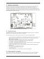
Wiring the ADSP-21992 board
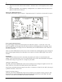
The layout of the board is given in figure 3. Important are that J17 t/m J20 are closed and J12 is open.
Figure 3: Board layout
Power supply and powering up
For power supply a EZ-kit Lite board requires two stable DC voltages: +5 Volt and -5 Volt. The
power is supplied onto the upper-left side of the board; this will be prepared by the assistants. Upon
switching on, proper power supply levels are indicated by four red LED indicators (CR1-CR4) near
the power connectors.
There is a fourth LED indicator (CR5) close to the reset button (S1) which lights up upon resetting the
board. It takes approximately 10 seconds after reset or power-on for this LED to light. If not, call an
assistant.
Peripherals
The peripherals of the board can be connected to the plant by the means of various headers and
jumpers. This section describes every one of them and also gives some extra information to keep into
account when using every specific in- or output in your model.
Analogue to Digital Input
The ADC ports on the ADSP board consist of one 8 channel, 14 bit analogue to digital converter. The
ADC connector is P4, and can be found at the left side of the board.
Note: Keep in mind that the input range for the ADC’s is limited to 2 Volts! For the ADC, this range is
symmetric: between -1 and 1 Volt.
Digital to Analogue Output
The DAC ports on the ADSP board consist of one 8 channel, 12 bit digital to analog converter. This
DA converter is connected through the SPI (Serial Peripheral Interface) port of the DSP. The DAC
connector is P5, and can be found at the left side of the board.
University of Twente
31
Note: Keep in mind that the input range for the DAC’s is limited to 2 Volts! For the DAC, this range is
not symmetric: between 0 and 2 Volt. This means that writing a 0 into a DAC register causes +1 Volt
on the channel. This also means that it is not possible to drive a DC motor in both directions. To solve
this issue, build a voltage level shifter by using one of the opamps.
Digital I/O
Connector P8 (upper side of the board, labels PF0-PF15) can be used to connect the digital I/O. All
pins can be programmed as input or output, with some restrictions. Some pins cannot be used, they are
PF2, PF3 and PF15.
PWM Output
For accessing the PWM signals, connect the following pins to the input of a power: The direction
signal from PF15 (on P8) and the PWM block and ground signals from AUX0 and DGND (on P10)
respectively.
Note: For driving motors, power amplification is necessary. Usually, the PWM unit along with an Hbridge circuit is used for that. Examples are available.
Encoder interface
On the upper-right side of the board are jumpers 28 and 29. These two inner contacts are used for two
phase leads of an encoder cable.
Note: By the implementation of the encoder drivers, upon the start of the on-board code, the encoder
output value is set to zero. Polarity of the encoder phases can be chosen arbitrarily. This polarity is
later brought in accordance with the positive orientation of remaining model orientations. Thus, after
one series of experiments with logged data polarity of the encoder input can be altered.
Code generation, downloading and running
Now we have a fully functioning controller it is time to generate code, download it into
the processor and run!
Before we continue, there are a few remarks:
• Before switching on power to the board or its peripherals, consult one of the assistants. No
special safety measures are taken, so wrong connections might ruin the (expensive!) board.
• Event specification functions ( *event() ) are not supported. When using sources, you have to
remove the *event() functions.
• Take care that all code that will be executed on the ADSP board is in one submodel, and that
all other parts (like DAC’s) are outside this submodel. Also take care not to use more inand/or outputs in your submodel than connections are available on the board.
Code generation
Either in the 20Sim editor or in the simulator, specify the path to the code generation descriptor file
(Targets.ini). You do this only once. Choose an appropriate sampling frequency for the onboard code.
Specify this frequency in the simulator by entering the value in the Discrete System tab in the Run
properties dialog box. Usually, 1 kHz is sufficient. Keep in mind that if you are using digital filters
you don’t forget to recalculate its coefficients when changing this value.
Still in the 20Sim simulator window, choose Tools - Real Time Toolbox - C-Code Generation. See
figure 4. Check whether the CCE target is selected and select the appropriate submodel as well.
Optionally change the target directory and click ’OK’ to continue.
Control Engineering
32
Figure 4: C-Code Generation in the 20Sim simulator
Connect the dots
After a few moments you should see a new windows application called Hardware connector (see
figure 5), in which you can connect all input and output ports of your submodel to a physical
peripheral. The names of the inputs and output ports are taken from your 20Sim model. First, add a
device by choosing Add in the upper half of the screen and selecting the ADSP21992.xml file from the
location provided by the assistants.
Figure 5: Hardwareconnector at first startup
You now can map ports from your submodel onto peripherals. You can toggle the view of inputs and
outputs by clicking on the inputs or outputs button. Now, for each of the ports, follow these steps (see
figure 6):
•
•
•
•
Click on the desired input or output
Click connect
Choose the appropriate Device, IO Kind and Channel from each list
Click Apply
When you’re done, click Continue.
University of Twente
33
Note: Although you can select Digital I/O channels 2 and 3, they cannot be used! Also, think about
selecting every Digital I/O channel for either input or output!
Figure 6: Window to connect each port to a physical channel
Downloading and running
After the hardware connector, a compiler assistant is started to change the source code from 20Sim in
such a way that it can run on the ADSP board with the appropriate ports connected to the right
perherals. After that, it starts compilers, linkers and other tools to create the file you can load into the
ADSP board. You can follow this process in the lower half of the dialog. When finished, the compiler
assistant will display a “Ready” dialog. You can check if everything went well by looking at the last
line of the output from the compiler assistant. It should say 0 errors (see figure 7).
Figure 7: When done, the compiler assistant
should say it finished without an error
Now, start the VisualDSP++ environment. Choose File - Load program. In the next dialog box, choose
the runme.dxe file from the directory you just created the code into. When download is finished, you
may run the code on the ADSP board (Press F5 in VisualDSP++, or choose Debug - Run).
Control Engineering
34
University of Twente
35
Appendix B – XML Files
ADSP21992.xml
The ADSP21992.xml file contains the hardware description and functions to get the functions of the
ADSP processor to work. See section 4.2.1.
CCE.xml
The CCE.xml file contains information for the hardware connector to work. It contains some variables
which will be changed by 20Sim in the code generation process, for instance %GENERATION_DIR% and
%NUMBER_VARIABLES%. See section 4.2.
Control Engineering
36
University of Twente
37
Appendix C – C source files
submod.c
In this file, the submodels are calculated, initialized and terminated. The relevant parts of this file are
below. Note the non-standard 20Sim tags like %IO_INITIALIZE% or %IO_CLOSE%. These tags
will be replaced by the Hardware Connector.
/* the initialization function for submodel */
void %FUNCTIONPREFIX%InitializeSubmodel (XXDouble *u, XXDouble *y, XXDouble t)
{
// Open the devices
%IO_INITIALIZE%
/* initialization phase (allocating memory) */
%VARPREFIX%%XX_INITIALIZE% = XXTRUE;
%VARPREFIX%steps = 0;
%FUNCTIONPREFIX%ModelInitialize ();
%FUNCTIONPREFIX%%INTEGRATION_METHOD_NAME%Initialize ();
[ some of initialization left out ]
/* end of initialization phase */
%VARPREFIX%%XX_INITIALIZE% = XXFALSE;
}
/* the termination function for submodel */
void %FUNCTIONPREFIX%TerminateSubmodel (XXDouble *u, XXDouble *y, XXDouble t)
{
/* copy the inputs */
%VARPREFIX%%XX_TIME% = t;
%FUNCTIONPREFIX%CopyInputsToVariables (u);
/* calculate the final model equations */
%FUNCTIONPREFIX%CalculateFinal ();
/* set the outputs */
%FUNCTIONPREFIX%CopyVariablesToOutputs (y);
/* and terminate the model itself (releasing memory) */
%FUNCTIONPREFIX%ModelTerminate ();
%FUNCTIONPREFIX%%INTEGRATION_METHOD_NAME%Terminate ();
//Close the devices
%IO_CLOSE%
}
xxmain.c
This file contains the “main” function. This is the function that “runs” the target. It first initializes all
hardware, and then does the same for the submodel. Next, it enters a simple while loop in which it
reads all inputs, calculates the new state for the submodel and writes the output back to the desired
ports.
int main()
{
[ variable declaration left out ]
/* initialize the inputs and outputs with correct initial values */
%INITIALIZE_INPUTS%
%INITIALIZE_OUTPUTS%
Control Engineering
38
/* initialize the submodel itself */
%FUNCTIONPREFIX%InitializeSubmodel (u, y, %VARPREFIX%%XX_TIME%);
/* simple loop, the time is incremented by the integration method */
//while (%VARPREFIX%%XX_TIME% < %VARPREFIX%finish_time)
while(true)
{
%IO_READ_ROUTINE%
/* call the submodel to calculate the output */
%FUNCTIONPREFIX%CalculateSubmodel (u, y, %VARPREFIX%%XX_TIME%);
%IO_WRITE_ROUTINE%
}
/* perform the final calculations */
%FUNCTIONPREFIX%TerminateSubmodel (u, y, %VARPREFIX%%XX_TIME%);
/* and we are done */
return 0;
}
University of Twente
39
Appendix D
Targets.ini
; Generate CCE project for a selected Model
;
[ADSP21992HW]
targetName="Command and control for 20-sim model"
iconFile="CCE.ico"
description="C-Code generated for a CCE model in 20-sim version 3.5"
SubmodelSelection=TRUE
templateDirectory="Drive:\Path\to\Templates\ADSP21992"
%TEMPLATE_DIR%="Drive:\Path\to\Templates\ADSP21992"
templateFiles=xxfuncs.c;xxfuncs.h;xxinteg.c;xxinteg.h;xxinverse.c
templateFiles=xxmain.c;xxmatrix.c;xxmatrix.h;xxmodel.c;xxmodel.h;CCE.xml
templateFiles=xxsubmod.c;xxsubmod.h;xxtypes.h;variables.cce;variables.arg
templateFiles=adsp21992.c;adsp21992.h;2199x_ivt.dsp;SPI_DAC_21992.dsp;compile.bat
templateFiles=timer.c;timer.h;main.h;spi_dac.h;pll.dsp;adsp-21992.ldf
targetDirectory="Drive:\Path\to\%MODEL_NAME%"
postCommand="Drive:\Path\to\HardwareConnector.exe"
Compile.bat
@echo off
echo Building library file ...
cc219x -Os xxmodel.c xxfuncs.c xxsubmod.c xxinteg.c adsp21992.c spi_dac_21992.dsp
timer.c -build-lib -o libccode.dlb
echo Assembling ...
easm219x -proc ADSP-21992 -o 2199x_ivt.doj 2199x_ivt.dsp
easm219x -proc ADSP-21992 -o pll.doj pll.dsp
echo Building ADSP21992 object file ...
cc219x -Os -c xxmain.c -proc ADSP-21992 -o xxmain.doj
echo Linking ...
cc219x -Os 2199x_ivt.doj pll.doj
21992 -o runme.dxe
echo Done
Control Engineering
xxmain.doj -lccode -T ADSP-21992.ldf -proc ADSP-
40
University of Twente
41
Appendix E – Board layout and jumper settings
Board layout
Relevant jumper settings
Jumper
(JP#)
1
3
5
6
7
Default
setting
Closed
1-2 position
1-2 position
1-2 position
1-2 position
8
9, 10, 11
12
15, 16
18 – 21
1-2 position
Open
Closed
Closed
Open
Control Engineering
Setting with
ADSP-21992
Closed
1-2 position
2-3 position
1-2 position
1-2 position (=LO PWM)
2-3 position (=HI PWM)
2-3 position
Open
Open (for 160MHz)
Closed
Closed (to connect to P9)
Meaing
Connects AGND to DGND
Internal / external Vref source
Disable / enable PWMTRIP
PWM Switched Reluctance mode selection
PWM polarity selection
Enable / disable AUXTRIP
Boot mode selection
PLL Bypass
SPI DAC selection
RS232 circuit jumpers
42
References
ADSP (2002a), ADSP-21992 EZ-KIT LITE Evaluation System Manual, Analog Devices, Inc.,
Norwood, Mass.
ADSP (2002b), ADSP 21992 Mixed Signal DSP Data Sheet,
http://www.analog.com/UploadedFiles/Datasheets/637820587ADSP-21992_pra.pdf.
ADSP (2002c), VisualDSP++ 3.0 C/C++ Compiler and Library Manual for ADSP-219x DSPs,
revision 4.0, Analog Devices, Inc., Norwood, Mass.
Buit, E. (2005), PC104 stack mechatronic control platform, MSc thesis, no 009CE2005, Control
Laboratory, University of Twente, Enschede.
Groothuis, M.A. (2001), 20-sim code generation for PC/104 target, Individual Design Report, no
009R2001, University of Twente, Enschede.
Mocking, C. (2002), 20-sim code generation for ADSP-21990 EZ-KIT, Individual Design Assignment,
no 040CE2002.
W3C (2004), Extensible Markup Language, http://www.w3.org/XML/Core.
University of Twente