1
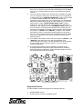
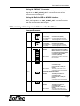
ZK-HC08EY-A
Starter Kit for Freescale
MC68HC908EY Family
(32-Pin QFP ZIF Socket)
User’s Manual
1. Introduction
Overview
The ZK-HC08EY-A Starter Kit has been designed for the evaluation of
the Freescale MC68HC908EY family and the debugging of user
applications. The ZK-HC08EY-A Starter Kit can be used as a standalone
application, or via its built-in USB to MON08 bridge, or together with an
external debugger through a MON08-compatible connection.
Starter Kit Features
The ZK-HC08EY-A Starter Kit features the following sections.
1.
An “MCU” section containing:
An MC68HC908EY16 microcontroller (in 32-pin QFP package,
already programmed with a demo application—in addition, you
can also use any other pin-to-pin-compatible device);
SofTec Microsystems
E-mail (general information): [email protected]
E-mail (marketing department): [email protected]
E-mail (technical support): [email protected]
Copyright © 2005 SofTec Microsystems®
DC00920
Web: http://www.softecmicro.com
Important
SofTec Microsystems reserves the right to make improvements to its products, their documentation and software routines, without notice. Information
in this manual is intended to be accurate and reliable. However, SofTec Microsystems assumes no responsibility for its use; nor for any infringements
of rights of third parties which may result from its use.
SOFTEC MICROSYSTEMS WILL NOT BE LIABLE FOR DAMAGES RESULTING FROM LOSS OF DATA, PROFITS, USE OF PRODUCTS, OR
INCIDENTAL OR CONSEQUENTIAL DAMAGES, EVEN IF ADVISED OF THE POSSIBILITY THEREOF.
Trademarks
Freescale™ and the Freescale logo are trademarks of Freescale Semiconductor, Inc.
Metrowerks and CodeWarrior are trademarks or registered trademarks of Metrowerks Corp.
Metrowerks is a wholly-owned subsidiary of Freescale Semiconductor.
Microsoft and Windows are trademarks or registered trademarks of Microsoft Corporation.
PC is a registered trademark of International Business Machines Corporation.
Other products and company names listed are trademarks or trade names of their respective companies.
ZK-HC08EY-A User's Manual
ZIF socket for the microcontroller;
A connector area to access the I/O pins of the microcontroller
for expansion prototyping;
Two clock sources: a 16 MHz clock module, a 8 MHz crystal
and a provision to use PTC3 and PTC4 as normal I/O,
selectable via the “OSC SEL” jumper;
A connector (J105) with RST_IN# and RST_OUT# signals.
2.
3.
4.
5.
6.
A “POWER SUPPLY” section which accepts a 12 V DC voltage
(used for the LIN transceiver) and provides a regulated VDD voltage
for the rest of the board. A jumper (“VDD SEL”) allows two different
microcontroller VDD voltages (3.3 V or 5.0 V) to be selected. A
circuitry (driven by the “MON08 CONNECTORS” and “USB TO
MON08 INTERFACE” sections of the board) is present which allows
the automatic power on and off of the board for entering the “monitor
mode”. An additional linear power supply regulator provides the 5.0
V voltage required by the “USB TO MON08 INTERFACE” section.
A built-in “USB TO MON08 INTERFACE” section which allows the
host PC to communicate with the microcontroller through a standard
USB interface. USB 2.0 is fully supported. When using an external
in-circuit debugger (via the “MON08” or “EMON08” connectors),
the “USB TO MON08 INTERFACE” circuitry must be bypassed by
removing all of the “ENA” jumpers in this area.
Two connectors for external in-circuit debugging/programming. Even
though the Starter Kits feature a built-in USB to MON08 interface,
two additional, separate MON08 connectors are present which allow
an external in-circuit debugger to be used. The “EMON08”
(Enhanced MON08) connector is used by in-circuit debugging tools
such the Freescale ICS system or the SofTec Microsystems
inDART-HC08; other tools, instead, use the “MON08” connector.
If you use an external in-circuit debugger/programmer, an additional
“VDD CTRL” connector allows you to control the Starter Kit’s VDD
voltage using the external tool’s power control. The output
impedance (both low and high) of the external tool driving the “VDD
CTRL” connector’s VDD_CTRL signal is not important.
A “RESET” section containing the push-button connected to the
MCU’s reset pin through a basic RC network.
An “INPUTS” section containing:
Four push-buttons, together with jumpers to connect/disconnect
them to/from the microcontroller’s PTA[4..1] lines;
A potentiometer, together with a jumper to connect/disconnect it
to/from the microcontroller’s PTB7/AD7 pin.
7.
8.
An “OUTPUTS” section containing eight high-efficiency (low-current)
LEDs connected to PTB[5..0] and PTC[1..0] lines, together with eight
jumpers to connect/disconnect each of the eight LEDs to/from their
respective PTB or PTC pins.
A “RS-232” section providing one RS-232 channel connected to the
microcontroller’s SCI serial communication interface. The
microcontroller’s PTE0/TXD and PTE1/RXD lines used by the RS232 channel are shared with the LIN transceiver’s RX and TX lines.
Use the “RXD SEL” and “TXD SEL” jumpers in the “SERIAL
SETTINGS” section of the board to select whether to use the RS-
Page 2
ZK-HC08EY-A User's Manual
232, LIN, or to free the microcontroller’s PTE0/TXD and PTE1/RXD
lines. A 9-pin, D-Sub female connector is provided for the RS-232
channel.
9. The “LIN” section contains one LIN transceiver, capable of a speed
of up to 100 Kbps in fast mode. The LIN node can be configured as
a master node via the “MASTER NODE ENA” jumper, which inserts
a 3.3 KOhm resistor between the LIN bus line and the LIN
transceiver power supply line. The LIN transceiver can be powered
either by the Starter Kit’s internal 12 V DC reference, or by the LIN
network itself, via the “TRANSCEIVER SUPPLY SEL” jumper.
Analogously, the LIN network can be supplied by the Starter Kit’s
internal 12 V DC reference via the “LIN SUPPLY ENA” jumper. The
microcontroller’s PTE0/TXD and PTE1/RXD lines used by the LIN
transceiver are shared with the RS-232 transceiver’s TXD and RXD
line. Use the “TXD SEL” and “RXD SEL” jumpers in the “SERIAL
SETTINGS” section of the board to select whether to use the RS232, LIN, or to free the microcontroller’s PTE0/TXD and PTE1/RXD
lines. A 3x1 male header connector is provided to interface to an
external LIN bus.
10. The “SERIAL SETTINGS” section has two jumpers (“TXD SEL” and
“RXD SEL”) that allow the use of the SCI peripheral of the
microcontroller to be chosen. The SCI peripheral can be connected
to the LIN node or to the RS-232 channel , or can be freed by
removing all jumpers.
11. A prototype area features both a standard, thru-hole area (for
mounting traditional components) and a SMD area (for soldering
SMD components). Additionally, all of the board’s supply lines (12 V,
5V, VDD and GND lines) are provided.
2
9
4
8
10
3
1
6
5
11
7
The ZK-HC08EY-A Starter Kit
Supported Devices
The ZK-HC08EY-A Starter Kit supports the following devices:
MC68HC908EY family;
And any future pin-to-pin compatible device.
Page 3
ZK-HC08EY-A User's Manual
Recommended Reading
Freescale HC08 microcontroller-specific datasheets;
SK-HC08 and ZK-HC08 Series Starter Kit User’s Manual;
ZK-HC08EY-A Schematic.
2. The “RST_IN/RST_OUT” Connector
Introduction
All of the HC08 family devices feature a monitor code resident in ROM
which, through a serial communication line, allows the programming and
the in-circuit debugging of the user application. The monitor code is
executed in “monitor mode”; the user application is executed in “user
mode”.
To enter the monitor mode some microcontroller lines must be properly
driven. In the case of the MC68HC908EY family, these lines are PTA0
(serial communication line), PTA1, PTB3, PTB4 and PTB5.
Additionally, to enter the monitor mode, a high-level voltage signal
(VTST) must be generated on the IRQ and RST pins of the
microcontroller. In the case of the MC68HC908EY family, the VTST
voltage is typically 9.1 V.
The “RST_IN#/RST_OUT#” Connector
The “RST_IN#/RST_OUT#” connector, in the “MCU” section of the
board, features the RST_IN# and RST_OUT# signals.
Depending on what in-circuit debugger/programmer you are using (builtin USB to MON08 interface, external tool connected to the “EMON08”
connector or external tool connected to the “MON08” connector) the
RST_IN# and RST_OUT# signals assume different meanings.
Using the “EMON08” Connector
Interfacing an external in-circuit debugger/programmer via the
“EMON08” connector allows the number of wasted lines required to
enter the monitor mode and executing the monitor code to be reduced.
In addition to the RST# line, the “EMON08” connector features two
special lines, RST_IN# and RST_OUT#, which allow your target
application to be interfaced to the target microcontroller’s reset line
without worrying about the high voltage that is generated on the RST#
line.
When using the “EMON08” connector:
The RST_OUT# signal in the “RST_IN#/RST_OUT#” connector is
the reset signal generated by the external in-circuit
debugger/programmer to the target system: it can be GND or open
drain.
The RST_IN# signal is the reset signal generated by your target
application: it is adapted by the external in-circuit
debugger/programmer which properly drives the microcontroller’s
RST# line.
Page 4
ZK-HC08EY-A User's Manual
Using the “MON08” Connector
When using the “MON08” connector, the RST_IN# and RST_OUT#
signals in the “RST_IN#/RST_OUT#” connector coincide with the
microcontroller’s RST# signal.
Using the Built-In USB to MON08 Interface
When using the built-In USB to MON08 Interface, the RST_IN# and
RST_OUT# signals in the “RST_IN#/RST_OUT#” connector coincide
with the microcontroller’s RST# signal.
3. Summary of Jumper and Connector Settings
Jumpers Summary
Name
Reference
Description/Pinout
J107
1
2
OSCILLATOR SELECTION
3
4
5
6
1
2
3
4
5
6
J108
J109
J110
1
1
1-2 (CLOCK)
Clock selected (default)
2-3 (CRYSTAL) Crystal configuration selected
4-5 (USER)
PTC4 configured as normal I/O
OSCILLATOR SELECTION
1-2 (CLOCK)
Clock selected (default)
2-3 (CRYSTAL) Crystal configuration selected
4-5 (USER)
PTC3 configured as normal I/O
EMON08 CONNECTOR
Installed
Not Installed
J201
When using the built-in USB to
MON08 interface or an external
in-circuit debugger/programmer
connected to the “MON08”
connector (default)
When using an external in-circuit
debugger/programmer connected to
this connector
PTA1 PUSH-BUTTON ENABLE
Installed
J202
The PTA1 push-button is
connected to the
microcontroller’s PTA1 pin
(default)
Not Installed
The PTA1 push-button is not
connected to the microcontroller
PTA2 PUSH-BUTTON ENABLE
Installed
J203
The PTA2 push-button is
connected to the
microcontroller’s PTA2 pin
(default)
Not Installed
The PTA2 push-button is not
connected to the microcontroller
PTA3 PUSH-BUTTON ENABLE
Installed
Not Installed
The PTA3 push-button is
connected to the
microcontroller’s PTA3 pin
(default)
The PTA3 push-button is not
connected to the microcontroller
Page 5
ZK-HC08EY-A User's Manual
Name
Reference
Description/Pinout
PTA4 PUSH-BUTTON ENABLE
J204
Installed
The PTA4 push-button is
connected to the
microcontroller’s PTA4 pin
(default)
Not Installed
The PTA4 push-button is not
connected to the microcontroller
POTENTIOMETER ENABLE
J205
Installed
Not Installed
J206
LED ENABLE
1
Installed
Not Installed
J302
1
2
3
J304
1
2
1-2 (3V3)
VDD = 3.3 V
2-3 (5V)
VDD = 5 V (default)
RXD SELECTION
1-2 (LIN)
2-3 (RS-232)
1
2
Each jumper, when installed,
connects a LED to the respective
microcontroller’s pin (default)
The LEDs are not connected to the
microcontroller.
VDD SELECTION
3
J305
The potentiometer is connected
to the microcontroller’s PTB7 pin
(default)
The potentiometer is not connected
to the microcontroller
Microcontroller’s PTE1/RXD pin
connected to LIN transceiver
Microcontroller’s PTE1/RXD pin
connected to RS-232 transceiver
(default)
TXD SELECTION
1-2 (LIN)
3
2-3 (RS-232)
Microcontroller’s PTE0/TXD pin
connected to LIN transceiver
Microcontroller’s PTE0/TXD pin
connected to RS-232 transceiver
(default)
LIN SUPPLY ENABLE
J306
Installed
J307
1
2
3
J308
LIN bus is powered by the Starter
Kit’s internal 12 V DC voltage
(default)
Not Installed
LIN bus is self-powered
LIN TRANSCEIVER SUPPLY SELECTION
1-2 (12V)
LIN transceiver is supplied by the
Starter Kit’s internal 12 V DC
voltage (default)
2-3 (LIN NETWORK)
LIN transceiver is supplied by the
LIN bus’ VBAT line
LIN MASTER NODE ENABLE
Installed
Not Installed
LIN master node (default)
LIN slave node
Page 6
ZK-HC08EY-A User's Manual
Name
Reference
Description/Pinout
J402
1
USB TO MON08 ENABLE
Installed
Not Installed
The USB to MON08 interface is
enabled
The USB to MON08 interface is
disabled
Connectors Summary/Pinout
Name
Reference
J101,
J102,
J103,
J104
J105
MCU I/O Connectors
See schematic for pin explanation
RST_IN# and RST_OUT#
1
2
1. RST_IN#
2. RST_OUT#
Ground Test Point
J106
J109
J110
Description/Pinout
EMON08 Connector
1
1
2
3
4
5
6
7
8
9
10
11
12
13
14
15
16
1. RST#
EMON08 Connector
1.
2.
3.
4.
5.
6.
7.
8.
9.
10.
11.
12.
13.
14.
15.
16.
RST_OUT#
GND
RST_IN#
RST#
TGT_IRQ#
IRQ#
TGT_PTA0
PTA0
TGT_PTA1
PTA1
TGT_PTB3
PTB3
TGT_PTB4
PTB4
TGT_PTB5
PTB5
Page 7
ZK-HC08EY-A User's Manual
Name
Reference
Description/Pinout
J111
1
2
MON08 Connector
3
4
5
6
7
8
9
10
11
12
13
14
15
16
J112
1
2
J301
2
1. N.C.
2. GND
3. N.C.
4. RST#
5. N.C.
6. IRQ#
7. N.C.
8. PTA0
9. N.C.
10. PTA1
11. N.C.
12. PTB3
13. N.C.
14. PTB4
15. VDD_CTRL
16. PTB5
VDD CTRL
1. VDD_CTRL
2. GND
12 V DC Power Supply Input Connector
1
1. 12 V DC
2. GND
Ground Test Point
J303
1
J309
3
LIN Connector
J310
1. VBAT – LIN Bus Power Supply
2. LIN – LIN Signal
3. GND
RS-232 Connector
J401
1. N.C.
2. TX
3. RX
4. N.C.
5. GND
6. N.C.
7. N.C.
8. N.C.
9. N.C.
USB Connector
9
5
6
1
1.
2.
3.
4.
5 V DC USB Bus Power Supply Line
USB DUSB D+
GND
Page 8


![[DRAFT] DEMO908JL16 User`s Manual](http://vs1.manualzilla.com/store/data/005639706_1-2a84cd2ce2f0b318fdb7aae7896f2a79-150x150.png)