1
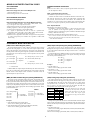
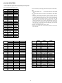
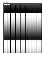
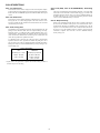
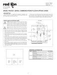
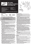
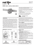
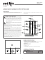
Bulletin No. PAXCDC4-E Drawing No. LP0502 Released 8/07 Tel +1 (717) 767-6511 Fax +1 (717) 764-0839 www.redlion.net MODEL PAXCDC -MODBUS OUTPUT OPTION CARD DESCRIPTION This product bulletin covers the MODBUS Communication Card for the PAX Meters. The card will allow the PAX Meter to transmit Display Values, Setpoints and Reset Values via MODBUS RS485 communication, in the RTU and ASCII modes. INSTALLING AN OPTION CARD TOP VIEW Caution: The option and main circuit cards contain static sensitive components. Before handling the cards, discharge static charges from your body by touching a grounded bare metal object. Ideally, handle the cards at a static controlled clean workstation. Also, only handle the cards by the edges. Dirt, oil or other contaminants that may contact the cards can adversely affect circuit operation. Warning: Exposed line voltage exists on the circuit boards. Remove all power to the meter AND load circuits before accessing the unit. 1. Remove the main assembly from the rear of the case. Squeeze the finger holds on the rear cover, or use a small scewdriver to depress the side latches to release it from the case. It is not necessary to separate the rear cover from the main circuit card. 2. Locate the option card connector for the type of option card to be installed. Hold the unit by the rear connector, not the display board, when installing an option card. 3. Install the option card by aligning the option card connector with the slot in the rear cover. The cards are keyed by position with different main board connector locations. Be sure the connector is fully engaged and the tab on the option card rests in the alignment slot on the display board. 4. Slide the assembly back into the case. Be sure the rear cover latches fully into the case. 5. Apply the option card label to the bottom side of the meter. Do not cover the vents on the top surface of the meter. The surface of the case must be clean for the label to adhere properly. Apply the label to the area designated by the large case label. 6. See manual for wiring connections and programming procedures. MODBUS SPECIFICATIONS 1. Type: RS485; RTU and ASCII MODBUS modes 2. Isolation To Sensor & User Input Commons: 500 Vrms for 1 minute. Working Voltage: 50 V. Not isolated from all other commons. 3. Baud Rates: 300 to 38400. 4. Data: 7/8 bits 5. Parity: No, Odd, or Even 6. Addresses: 1 to 247. 7. Transmit Delay: Programmable; See Transmit Delay explanation. ORDERING INFORMATION MODEL PAXCDC 1 DESCRIPTION PART NUMBER PAX MODBUS Output Card PAXCDC40 PAX MODBUS Output Card with RJ11 Connector PAXCDC4C RS485 COMMUNICATIONS RECEIVING DEVICE PAX METER The RS485 communication standard allows the connection of up to 32 devices on a single pair of wires, distances up to 4,000 ft. and data rates as high as 10M baud (the PAX is limited to 19.2k baud). The same pair of wires is used to both transmit and receive data. RS485 is therefore always half-duplex, that is, data cannot be received and transmitted simultaneously. +5V 33K Transmit Enable 12 13 B(-) A(+) 33K 14 COMM. * 15 NC * OPTIONAL Terminal Block Connection Figure Extended Comms Connection Figure SERIAL SET-UP DIP SWITCH OPERATION For the serial bank, the following settings apply: Serial port configuration is accomplished through two banks of DIP switches on the MODBUS card. The bank of 8 switches sets the Unit Address, the bank of 7 switches sets the Serial port parameters (ASCII/RTU, 7/8 bits, Parity, and Baud rate). Changes to the switch settings are only detected on power-up of the unit. After changing a switch setting, power to the unit must be cycled for the new switch setting to take effect. SWITCH SETTINGS AVAILABLE 1 OFF: ASCII ON: RTU RTU 2 OFF: 7 Bits ON: 8 Bits 8 Bits 3 OFF: None ON: Parity No Parity 4 OFF: Even ON: Odd 5 Baud Rate 6 Baud Rate 7 Baud Rate OFF (See Baud Rate Switch Selections) BAUD RATE SWITCH SELECTIONS Both unit address and serial set-up are set via DIP switches on the MODBUS option card. See the DIP switch setting table for more details on these DIP switches. For the Unit Address bank, the high order bit is switch 1, and the ON position is a ‘1’, the OFF position is a ‘0’. Legal unit addresses are 1 to 247. When a Unit Address of 0 is selected, the card responds to Unit Address 1. When a Unit Address of 248 through 255 is selected, the card responds to Unit Address 247. 2 FACTORY SETTINGS 5 6 7 38400: ON ON ON 19200: ON ON OFF 9600: ON OFF ON 4800: ON OFF OFF 2400: OFF ON ON 1200: OFF ON OFF 600: OFF OFF ON 300: OFF OFF OFF 9600 MODBUS SUPPORTED FUNCTION CODES OTHER SUPPORTED FUNCTIONS COIL FUNCTIONS FC04: Returns the same values as FC03, except the register number starts with “3” (Ex: Pax Input Hi is 30001) FC01: Read Coils FC05: Force Single Coil, FC15: Force Multiple Coils. 1. Valid coil addresses are 1-49. 2. Block starting point can not exceed coil 49. FC08 – Fetch Comm. Event Counter. The MODBUS response breaks down as follows: “:010804”<TOT HI><TOT LO><GOOD HI><GOOD LO>XX<CR><LF> The “TOT HI” and “TOT LO” values are the total number of messages that were received, that started with the card’s address. The “GOOD HI” and “GOOD LO” are “good” messages (correct address, parity, and checksum). The values are reset on power up and every time the FC08 function is requested. HOLD REGISTER FUNCTIONS FC03: Read Holding Registers. FC06: Preset Single Register, FC16: Preset Multiple Registers. 1. Valid register address are 40001 – 40039, 40041, 40042, 41001 – 41010. 2. Up to 16 registers can be requested at one time. 3. Block starting point can not exceed the register boundaries. 4. Holding registers are a mirror of Input registers (FC04). 5. Unused registers will return a value of HEX <8000>. 6. If a register is implemented, but does not exist for a particular unit configuration (such as SP3, SP4) a value of HEX <0000> will be returned. 7. Registers 41001 – 41010 contain the slave ID. See FC17. 8. Broadcast write is supported for FC06 & FC16. Register writes using address “0” will be recognized by the MODBUS card, regardless of address DIP switch setting. FC17 - Report Slave ID. The following is sent upon FC17 request: Unit Address, 17 (FC code), RLC-PAX(I or ?) 00?0, 0100 (for code version 1.00), 16 (number of read supported registers), 16 (number of write supported registers), 00 (number of registers available for GUID/Scratch pad memory), checksum of the string. The following is the HEX of a PAXI (with unit address of 247): :<F7><11><14><52><4C><43><2D><50><41><58><49><30><30><3F> <30><01><00><00><10><00><10><00><00><XX><CR><LF> XX is the LRC Checksum PAX MANUAL MODE DESCRIPTION (CSR) Control Status Register [40021] (SOR) Setpoint Output Register [40038] (PAXI/PAXCK) The Control Status Register is used to directly control the meter’s outputs (setpoints and analog output), or view the state of the setpoint outputs and the status of the temperature sensor (PAXT only). The register is bit mapped with each bit position within the register assigned to a particular control function. The control functions are invoked by writing to each bit position. The bit position definitions are: This register is used to view or change the states of the setpoint outputs. Reading from this register will show the present state of all the setpoint outputs. A “0” in the setpoint location means the output is inactive and a “1” means the output is active. In Automatic Mode (See MMR Description), the meter controls the setpoint output state. In Manual Mode, writing to this register will change the output state. The bit position definitions are: bit 0: SP1 Output bit 1: SP2 Output 0 = output off bit 2: SP3 Output 1 = output on bit 3: SP4 Output bit 4: Manual Mode 0 = automatic mode 1 = manual mode bit 5: Always stays 0, even if 1 is sent. bit 6: Sensor Status (PAXT only) 0 = sensor normal 1 = sensor fail bit 7: Always stays 0, even if 1 is sent. bit 0: SP1 bit 1: SP2 bit 2: SP3 bit 3: SP4 Examples: 1. Turn all outputs on: Value to write to holding register 40038: 000Fh. 2. Turn outputs 1, 3 on: Value to write to holding register 40038: 0005h. 3. Turn all outputs off: Value to write to holding register 40038: 0000h. In Manual Mode, the setpoint outputs are defined by the values written to bits b0, b1, b2, b3; and the analog output is defined by the value written to the AOR. Internal control of these outputs is then overridden. In automatic mode, the setpoint outputs can only be reset off. (MMR) Auto/Manual Mode Register [40036] (PAXI/PAXCK) (AOR) Analog Output Register (Not PAXCK) This register sets the controlling mode for the outputs. In Auto Mode (0) the meter controls the setpoint output. In Manual Mode (1) the outputs are defined by the registers SOR. When transferring from auto mode to manual mode, the meter holds the last output value (until the register is changed by a write). Each output may be independently changed to auto or manual. Select values to place in manual mode by writing appropriate value to holding register 40036. The bit position definitions are: bit 0: Analog Output bit 1: SP4 bit 2: SP3 bit 3: SP2 bit 4: SP1 0 = Auto Mode 1 = Manual Mode The Analog Output Register controls the analog output of the meter. The manual mode must first be engaged by setting bit 4 of the CSR (PAX) or bit 0 of the MMR (PAXI). The range of values of this register is 0 to 4095, which corresponds to 0 mA, 0 V and 20 mA, 10 V; respectively. If a value larger than 4095 is written to the AOR register, 4095 will be loaded. The table lists correspondence of the output signal with the register value. Register Value PAXCK PAXI bit 0: SP4 bit 1: SP3 bit 2: SP2 bit 3: SP1 0 = Output off 1 = Output on 0 1 2047 4094 4095 0 = Auto Mode 1 = Manual Mode Examples: 1. Select manual mode for all outputs (PAX): Value to write to holding register 40021: 0010h 2. Select manual mode for all outputs and AOR (PAXI, PAXCK): Value to write to holding register 40036: 001Fh Output Signal* I (mA) 0.000 0.005 10.000 19.995 20.000 V (V) 0.000 0.0025 5.000 9.9975 10.000 *Due to the absolute accuracy rating and resolution of the output card, the actual output signal may differ 0.15% FS from the table values. The output signal corresponds to the range selected (20 mA or 10 V). Writing to this register while the meter is in the manual mode causes the output signal to update immediately. While in the automatic mode, this register may be written to, but the output will not update until the meter is placed in manual mode. Examples: 1. Set output to full scale: Value to write to holding register 40020 (PAX) or 40037 (PAXI): 0FFFh (4095). 2. Set output to zero scale: Value to write to holding register 40020 (PAX) or 40037 (PAXI): 0000h (0). 3 HOLDING REGISTERS Values less than 65,535 will be in (LO word). Values greater than 65,535 will continue into (HI word). Negative values are represented by two’s complement of the combined (HI word) and (LO word). * See Coil Table for register mapping and Coil Descriptions for functionality. SETTING HOLDING REGISTER PAX 4 ACCESS 40001: Input (HI) Read Only 40002: Input (LO) Read Only 40003: Total (HI) Read Only 40004: Total (LO) Read Only 40005: Min (HI) Read Only 40006: Min (LO) Read Only 40007: Max (HI) Read Only 40008: Max (LO) Read Only 40009: SP1 (HI) Read/Write 40010: SP1 (LO) Read/Write 40011: SP2 (HI) Read/Write 40012: SP2 (LO) Read/Write 40013: SP3 (HI) Read/Write 40014: SP3 (LO) Read/Write 40015: SP4 (HI) Read/Write 40016: SP4 (LO) Read/Write 40017: Polling1 * Read/Write 40018: Reset * 40019: TRX Delay 40020: AOR Notes: 1. Any registers marked with “——” are unused and will return a value of HEX <8000>. 2. If a value larger than 4095 is written to the AOR register, 4095 will be loaded. 3. TRX delay is the minimum time from the reception of the last character in the MODBUS Query until the response is started. The minimum delay value is equal to 2 character times (2 msec min.). The user can increase the delay time by writing to the TRX Delay register. Any value written to the TRX Delay register that is less than the value calculated at power up will be ignored. The TRX Delay value is stored in E2PROM memory. On power-up, the calculated value is compared to the value read back from the E2PROM. The greater of the 2 values will be used as the TRX Delay value and will be written to the TRX Delay register. 4. Numeric data is limited to value -19999 to 99999. 5. Numeric data is limited to the value listed for that parameter according to the meter’s literature. Read/Write 3 2 Read/Write Read/Write 40021: CSR Read/Write 40022: Terminate1 Read/Write HOLDING REGISTER SETTING 40001: CTA (HI) 40002: 40003: HOLDING REGISTER SETTING PAXI 5 SETTING PAXCK/PAXTM 5 SETTING ACCESS Timer (HI) Read/Write 40023: LDC (HI) SP4 Off (HI) Read/Write CTA (LO) Timer (LO) Read/Write 40024: LDC (LO) SP4 Off (LO) Read/Write CTB (HI) Counter (HI) Read/Write 40025: SP1 (HI) Timer Start (HI) Read/Write 40004: CTB (LO) Counter (LO) Read/Write 40026: SP1 (LO) Timer Start (LO) Read/Write 40005: CTC (HI) RTC Time (HI) Read/Write 40027: SP2 (HI) Counter Start (HI) Read/Write SP2 (LO) Counter Start (LO) Read/Write PAXI 5 SETTING PAXCK/PAXTM SETTING 5 ACCESS 40006: CTC (LO) RTC Time (LO) Read/Write 40028: 40007: RTE (HI) RTC Date (HI) Read/Write 40029: SP3 (HI) Timer Stop (HI) Read/Write 40008: RTE (LO) RTC Date (LO) Read/Write 40030: SP3 (LO) Timer Stop (LO) Read/Write 40009: Min (HI) SP1 (HI) Read/Write 40031: SP4 (HI) Counter Stop (HI) Read/Write 40010: Min (LO) SP1 (LO) Read/Write 40032: SP4 (LO) Counter Stop (LO) Read/Write 40011: Max (HI) SP2 (HI) Read/Write 40033: Polling1 * Polling1 * Read/Write 40012: Max (LO) SP2 (LO) Read/Write 40034: Polling2 * Polling2 * 40013: SFA (HI) SP3 (HI) Read/Write 40035: TRX Delay MMR AOR 3 TRX Delay Read/Write 3 Read/Write 40014: SFA (LO) SP3 (LO) Read/Write 40036: 40015: SFB (HI) SP4 (HI) Read/Write 40037: 40016: SFB (LO) SP4 (LO) Read/Write 40038: SOR SOR Read/Write 40017: SFC (HI) SP1 Off (HI) Read/Write 40039: Reset * Reset * Read/Write 40018: SFC (LO) SP1 Off (LO) Read/Write 40040: 2 MMR Read/Write RTC Day Read/Write 40019: LDA (HI) SP2 Off (HI) Read/Write 40041: Terminate1 Terminate1 Read/Write 40020: LDA (LO) SP2 Off (LO) Read/Write 40042: Terminate2 Terminate2 Read/Write 40021: LDB (HI) SP3 Off (HI) Read/Write 40022: LDB (LO) SP3 Off (LO) Read/Write 4 COIL TABLE PAX PAXI PAXCK COIL ADDRESS COIL NUMBER 01 0 SP1 Output 40021 (bit 0) SP1 Output 40038 (bit 0) SP1 Output 40038 (bit 0) 02 1 SP2 Output 40021 (bit 1) SP2 Output 40038 (bit 1) SP2 Output 40038 (bit 1) 03 2 SP3 Output 40021 (bit 2) SP3 Output 40038 (bit 2) SP3 Output 40038 (bit 2) 04 3 SP4 Output 40021 (bit 3) SP4 Output 40038 (bit 3) SP4 Output 40038 (bit 3) 05 4 Reset Max 40018 (bit 2) Reset Max 40039 (bit 2) ——- ——- 06 5 Reset Min 40018 (bit 3) Reset Min 40039 (bit 3) ——- ——- 07 6 ——- ——- Reset CNT A 40039 (bit 7) Reset Timer 40039 (bit 7) 08 7 ——- ——- Reset CNT B 40039 (bit 6) Reset Counter 40039 (bit 6) 09 8 ——- ——- Reset CNT C 40039 (bit 5) ——- ——- 10 9 Reset Total 40018 (bit 4) ——- ——- ——- ——- 11 10 Poll Input 40017 (bit 0) Poll CNT A 40033 (bit 0) Poll Timer 40033 (bit 0) 12 11 Poll Total 40017 (bit 1) Poll CNT B 40033 (bit 1) Poll Counter 40033 (bit 1) 13 12 Poll Max 40017 (bit 2) Poll MAX 40033 (bit 2) Poll SP2 40033 (bit 2) 14 13 Poll Min 40017 (bit 3) Poll MIN 40033 (bit 3) Poll SP1 40033 (bit 3) 15 14 Poll SP1 40017 (bit 4) Poll SP1 40033 (bit 4) Poll Timer Start 40033 (bit 4) 16 15 Poll SP2 40017 (bit 5) Poll SP2 40033 (bit 5) Poll Counter Start 40033 (bit 5) 17 16 Poll SP3 40017 (bit 6) Poll SP3 40033 (bit 6) Poll Timer Stop 40033 (bit 6) 18 17 Poll SP4 40017 (bit 7) Poll SP4 40033 (bit 7) Poll Counter Stop 40033 (bit 7) 19 18 Poll AOR 40017 (bit 8) Poll AOR 40033 (bit 8) Poll Day 40033 (bit 8) 20 19 Poll CSR 40017 (bit 9) Poll SOR 40033 (bit 9) Poll SOR 40033 (bit 9) 21 20 Term Total 40022 (bit 0) Poll CNT C 40033 (bit 10) Poll RTC Time 40033 (bit 10) 22 21 Term Max 40022 (bit 1) Poll RATE 40033 (bit 11) Poll RTC Date 40033 (bit 11) 23 22 Term Min 40022 (bit 2) Poll SFA 40033 (bit 12) Poll SP3 40033 (bit 12) 24 23 Term SP1 40022 (bit 3) Poll SFB 40033 (bit 13) Poll SP4 40033 (bit 13) 25 24 Term SP2 40022 (bit 4) Poll SFC 40033 (bit 14) Poll SP1 Off 40033 (bit 14) 26 25 Term SP3 40022 (bit 5) Poll LDA 40033 (bit 15) Poll SP2 Off 40033 (bit 15) 27 26 Term SP4 40022 (bit 6) Poll LDB 40034 (bit 0) Poll SP3 Off 40034 (bit 0) 28 27 Term AOR 40022 (bit 7) Poll LDC 40034 (bit 1) Poll SP4 Off 40034 (bit 1) 29 28 Term CSR 40022 (bit 8) Poll MMR 40034 (bit 2) Poll MMR 40034 (bit 2) 30 29 Response Delay 40017 (bit 10) Response Delay 40034 (bit 3) Response Delay 40034 (bit 3) 31 30 ——- ——- Term CNT A 40041 (bit 0) Term Timer 40041 (bit 0) 32 31 ——- ——- Term CNT B 40041 (bit 1) Term Count 40041 (bit 1) 33 32 ——- ——- Term CNT C 40041 (bit 2) Term RTC Time 40041 (bit 2) 34 33 ——- ——- Term Rate 40041 (bit 3) Term RTC Date 40041 (bit 3) 35 34 ——- ——- Term Min 40041 (bit 4) Term SP1 40041 (bit 4) 36 35 ——- ——- Term Max 40041 (bit 5) Term SP2 40041 (bit 5) 37 36 ——- ——- Term SFA 40041 (bit 6) Term SP3 40041 (bit 6) 38 37 ——- ——- Term SFB 40041 (bit 7) Term SP4 40041 (bit 7) 39 38 ——- ——- Term SFC 40041 (bit 8) Term SP1 Off 40041 (bit 8) 40 39 ——- ——- Term LDA 40041 (bit 9) Term SP2 Off 40041 (bit 9) 41 40 ——- ——- Term LDB 40041 (bit 10) Term SP3 Off 40041 (bit 10) 42 41 ——- ——- Term LDC 40041 (bit 11) Term SP4 Off 40041 (bit 11) 43 42 ——- ——- Term SP1 40041 (bit 12) Term Time Start 40041 (bit 12) 44 43 ——- ——- Term SP2 40041 (bit 13) Term Count Start 40041 (bit 13) 45 44 ——- ——- Term SP3 40041 (bit 14) Term Time Stop 40041 (bit 14) 46 45 ——- ——- Term SP4 40041 (bit 15) Term Count Stop 40041 (bit 15) 47 46 ——- ——- Term AOR 40042 (bit 0) Term MMR 40042 (bit 0) 48 47 ——- ——- Term MMR 40042 (bit 1) Term Day 40042 (bit 1) 49 48 ——- ——- Term SOR 40042 (bit 2) Term SOR 40042 (bit 2) COIL NAME MIRROR REGISTER COIL NAME 5 MIRROR REGISTER COIL NAME MIRROR REGISTER COIL DESCRIPTIONS Coils 1-4: Output Coils Coils 21-29 (PAX), Coils 31-49 (PAXI/PAXCK): Terminating Coils These coils are used to read or change the states of the Setpoint Outputs. To change the state of the output(s), the output(s) must be in manual mode. Refer to the CSR or MMR/SOR registers in the Manual Mode Description section. This set of coils determines what terminating character is sent to the PAX meter when a write command is executed. If the flag is 0, a $ is used as the terminating character and the value is not saved to E2PROM memory in the PAX. If the flag is 1, an * is used as the terminating character and the value is saved to E2PROM memory in the PAX. Coils 5-10: Reset Coils These coils are used to perform the Reset command for the values listed. Forcing the coil “on” causes the appropriate value in the unit to be reset. The coil is cleared after the command is executed, therefore, the coil value read will always be 0 (zero). Coil 30: Response Delay When a write command is issued, the new value is written to the PAX. If the coil is off, the MODBUS write response is not issued until the value is read back from the PAX. For MODBUS reads, if a polling coil is off, the response is not issued until the latest value is read back from the PAX. If the coil is set “on” the MODBUS response is issued as soon the received command is complete. The write coil is saved in E2PROM memory. Factory setting is on. Coils 11-29: Polling Coils The MODBUS card is continually requesting values from the PAX unit. The polling bit coils determine what values are requested during each loop. Setting the coils to “1” enables the card to poll that particular value. A “0” value disables it. Turning polling coils off allows the user to request fewer values and therefore decreases the internal loop time, which allows the values that are polled to be updated more often. If a MODBUS read is issued for any value, that value is automatically updated to the latest value, regardless of whether the polling bit is on or off. On power up, all values are updated regardless of Polling bit settings. Polling coil values are saved in E2PROM memory. Factory settings is “on” for all Polling coils. TYPICAL UPDATE TIMES** PAX PAXI/PAXCK All values (10) - 1.15 sec All values (19) - 900 msec 5 values - 500 msec 10 values - 480 msec 1 value - 100 msec 5 values - 230 msec 1 value - 52 msec **Update time is the typical time to update the internal memory provided no MODBUS requests are incoming. 6 This page intentionally left blank 7 LIMITED WARRANTY The Company warrants the products it manufactures against defects in materials and workmanship for a period limited to two years from the date of shipment, provided the products have been stored, handled, installed, and used under proper conditions. The Company’s liability under this limited warranty shall extend only to the repair or replacement of a defective product, at The Company’s option. The Company disclaims all liability for any affirmation, promise or representation with respect to the products. The customer agrees to hold Red Lion Controls harmless from, defend, and indemnify RLC against damages, claims, and expenses arising out of subsequent sales of RLC products or products containing components manufactured by RLC and based upon personal injuries, deaths, property damage, lost profits, and other matters which Buyer, its employees, or sub-contractors are or may be to any extent liable, including without limitation penalties imposed by the Consumer Product Safety Act (P.L. 92-573) and liability imposed upon any person pursuant to the Magnuson-Moss Warranty Act (P.L. 93-637), as now in effect or as amended hereafter. No warranties expressed or implied are created with respect to The Company’s products except those expressly contained herein. The Customer acknowledges the disclaimers and limitations contained herein and relies on no other warranties or affirmations. Red Lion Controls AP Red Lion Controls 20 Willow Springs Circle Red Lion Controls BV Printerweg 10 31, Kaki Bukit Road 3, #06-04/05 TechLink York PA 17406 NL - 3821 AD Amersfoort Singapore 417818 Tel +1 (717) 767-6511 Tel +31 (0) 334 723 225 Tel +65 6744-6613 Fax +1 (717) 764-0839 Fax +31 (0) 334 893 793 Fax +65 6743-3360