1
User Manual
PhotoniQ Series
IQSP584
128 Channel Data Acquisition System
Vertilon Corporation, 66 Tadmuck Road, Westford, MA 01886 / Tel: (978) 692-7070 / Fax: (978) 692-7010 / www.vertilon.com
User Manual
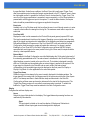
Disclaimer
Vertilon Corporation has made every attempt to ensure that the information in this document is accurate and complete.
Vertilon assumes no liability for errors or for any incidental, consequential, indirect, or special damages including,
without limitation, loss of use, loss or alteration of data, delays, lost profits or savings, arising from the use of this
document or the product which it accompanies.
Vertilon reserves the right to change this product without prior notice. No responsibility is assumed by Vertilon for any
infringements of patents or other rights of third parties which may result from its use. No license is granted by implication
or otherwise under the patent and proprietary information rights of Vertilon Corporation.
Copyright Information
© 2011 Vertilon Corporation
ALL RIGHTS RESERVED
-3Vertilon Corporation, 66 Tadmuck Road, Westford, MA 01886 / Tel: (978) 692-7070 / Fax: (978) 692-7010 / www.vertilon.com
PhotoniQ IQSP584 128 Channel Data Acquisition System
-4Vertilon Corporation, 66 Tadmuck Road, Westford, MA 01886 / Tel: (978) 692-7070 / Fax: (978) 692-7010 / www.vertilon.com
User Manual
Table of Contents
List of Figures ....................................................................................................................... 8
List of Tables......................................................................................................................... 9
Product Overview ............................................................................................................... 11
Features ........................................................................................................................... 11
Applications ...................................................................................................................... 12
Hardware .......................................................................................................................... 13
Software ........................................................................................................................... 14
Included Components and Software................................................................................. 15
Ordering Information......................................................................................................... 15
Hardware Accessories...................................................................................................... 16
Specifications...................................................................................................................... 17
System Specifications....................................................................................................... 17
General Timing Specifications .......................................................................................... 17
Trigger and Integration Specifications .............................................................................. 18
Miscellaneous Specifications............................................................................................ 19
Mechanical Specifications ................................................................................................ 19
PC System Requirements ................................................................................................ 19
Typical PET Setup............................................................................................................... 20
Theory of Operation............................................................................................................ 22
Charge Collection & Data Acquisition Channels ............................................................... 23
Configurable Preamp Cell................................................................................................. 23
Pipelined Parallel Processor............................................................................................. 24
Digital Signal Processor.................................................................................................... 25
Control and Acquisition Interface Software....................................................................... 26
Intelligent Triggering and Integration ................................................................................ 26
Edge Trigger........................................................................................................... 27
Internal Trigger ....................................................................................................... 27
Level Trigger........................................................................................................... 27
Input Trigger ........................................................................................................... 28
Pre-Trigger ............................................................................................................. 28
Cross Bank Triggering ............................................................................................ 29
Integration Delay and Period .................................................................................. 29
Boxcar Mode .......................................................................................................... 29
Boxcar Width .......................................................................................................... 29
Hardware Interface.............................................................................................................. 30
-5Vertilon Corporation, 66 Tadmuck Road, Westford, MA 01886 / Tel: (978) 692-7070 / Fax: (978) 692-7010 / www.vertilon.com
PhotoniQ IQSP584 128 Channel Data Acquisition System
Control and Acquisition Interface Software...................................................................... 32
Control Area...................................................................................................................... 35
Acquisition .............................................................................................................. 35
Processing .............................................................................................................. 36
System.................................................................................................................... 36
Integration............................................................................................................... 37
Trigger .................................................................................................................... 37
Event Data .............................................................................................................. 38
Display .................................................................................................................... 39
Real Time Display Area .................................................................................................... 41
Display .................................................................................................................... 41
Display Limit Adjust ................................................................................................ 41
Channels................................................................................................................. 41
Flip X....................................................................................................................... 41
Flip Y....................................................................................................................... 41
Transpose............................................................................................................... 41
Pull Down Menus .............................................................................................................. 42
File .......................................................................................................................... 42
System.................................................................................................................... 43
Processing .............................................................................................................. 47
Utilities .................................................................................................................... 49
Data Filtering ....................................................................................................................... 52
Spectral Filtering ............................................................................................................... 52
Band Definition ....................................................................................................... 53
Flag Definition......................................................................................................... 54
Discriminant Definition ............................................................................................ 55
2D Filtering ....................................................................................................................... 56
2D Filtering Definition.............................................................................................. 56
Log Files .............................................................................................................................. 57
Binary Log File Format...................................................................................................... 57
Event Packet Description.................................................................................................. 58
Format .................................................................................................................... 58
Header Word .......................................................................................................... 60
Signal Data ............................................................................................................. 60
Trigger / Time Stamp .............................................................................................. 60
Boxcar Width .......................................................................................................... 61
Front Panel ADC..................................................................................................... 61
External Word ......................................................................................................... 61
Packet Length......................................................................................................... 61
Minimum Packet Length ......................................................................................... 61
Converting a Binary Log File to Text................................................................................. 62
-6Vertilon Corporation, 66 Tadmuck Road, Westford, MA 01886 / Tel: (978) 692-7070 / Fax: (978) 692-7010 / www.vertilon.com
User Manual
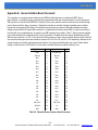
Configuration Tables .......................................................................................................... 63
User Configuration Table.................................................................................................. 63
Custom Configuration Table ............................................................................................. 68
Factory Configuration Table ............................................................................................. 68
DLL Function Prototypes ................................................................................................... 71
Function Prototypes.......................................................................................................... 71
Initialize:.................................................................................................................. 71
Close: ..................................................................................................................... 71
ControlInterface: ..................................................................................................... 71
DataInterface: ......................................................................................................... 72
ErrorHandler: .......................................................................................................... 73
LVDLLStatus: ......................................................................................................... 73
Error Cluster Initialization.................................................................................................. 73
Control Interface Commands............................................................................................ 74
Low Level USB Interface Description ............................................................................... 76
USB Device Defaults ........................................................................................................ 76
HID Implementation .......................................................................................................... 76
Report Format (IDs 0x01 and 0x11) ................................................................................. 77
Report Format (ID 0x22)................................................................................................... 78
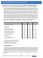
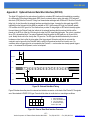
Appendix A: Sensor Interface Board Connector............................................................. 79
Appendix B: Optional High Voltage Supplies (HVPS001 / HVPS002 / HVPS701) ......... 80
Appendix C: Optional External Data Word Interface (DIO100)....................................... 81
-7Vertilon Corporation, 66 Tadmuck Road, Westford, MA 01886 / Tel: (978) 692-7070 / Fax: (978) 692-7010 / www.vertilon.com
PhotoniQ IQSP584 128 Channel Data Acquisition System
List of Figures
Figure 1: Model IQSP584 Front View.........................................................................13
Figure 2: Model IQSP584 Rear View .........................................................................13
Figure 3: PhotoniQ Control and Acquisition Software Front Panel.............................14
Figure 4: Typical Setup for PET Scanner ...................................................................20
Figure 5: PhotoniQ Pre-Trigger Timing ......................................................................21
Figure 6: PhotoniQ IQSP584 Functional Block Diagram ............................................22
Figure 7: Front End Preamp Cell................................................................................23
Figure 8: 32-Channel Pipelined Parallel Processor ....................................................24
Figure 9: DSP Functional Block Diagram ...................................................................25
Figure 10: Intelligent Trigger Module..........................................................................26
Figure 11: IQSP584 Front Panel ................................................................................30
Figure 12: IQSP584 Rear Panel.................................................................................30
Figure 13: Front Panel (Bar Graph Display) ...............................................................32
Figure 14: Front Panel (2D Single 8 x 8 Display) .......................................................33
Figure 15: Front Panel (2D Dual 8 x 8 Display)..........................................................34
Figure 16: Data Configuration Dialog Box ..................................................................43
Figure 17: High Voltage Supply Dialog Box ...............................................................45
Figure 18: General Purpose Output Dialog Box .........................................................46
Figure 19: Cross Bank Triggering Dialog Box ............................................................47
Figure 20: Gain Compensation Dialog Box ................................................................48
Figure 21: Diagnostic Report Dialog Box ...................................................................49
Figure 22: Log File Converter Dialog Box ..................................................................50
Figure 23: Select File Dialog Box ...............................................................................51
Figure 24: Band Definition Pane ................................................................................53
Figure 25: Flag Definition Pane..................................................................................54
Figure 26: Discriminant Definition Pane .....................................................................55
Figure 27: 2D Filtering Definition Pane.......................................................................56
Figure 28: Event Packet Format.................................................................................59
Figure 29: External Data Word Timing .......................................................................81
Figure 30: External Data Word Interface Connector ..................................................81
-8Vertilon Corporation, 66 Tadmuck Road, Westford, MA 01886 / Tel: (978) 692-7070 / Fax: (978) 692-7010 / www.vertilon.com
User Manual
List of Tables
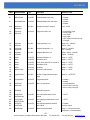
Table 1: Ordering Information (Configuration Options) ..............................................15
Table 2: System Specifications ..................................................................................17
Table 3: General Timing Specifications......................................................................17
Table 4: Trigger and Integration Specifications..........................................................18
Table 5: Miscellaneous Specifications .......................................................................19
Table 6: Mechanical Specifications ............................................................................19
Table 7: Binary Log File (ID Text Header Section).....................................................57
Table 8: Binary Log File (Config Table Section).........................................................57
Table 9: Binary Log File (Data Block Section)............................................................58
Table 10: Event Packet Signal Data Word Totals ......................................................58
Table 11: Event Packet Header Word........................................................................60
Table 12: Log File Data Formats................................................................................60
Table 13: User Configuration Table ...........................................................................67
Table 14: Custom Configuration Table.......................................................................68
Table 15: Factory Configuration Table .......................................................................70
Table 16: Control Interface Commands .....................................................................75
Table 17: USB Device Details....................................................................................76
Table 18: HID Report Descriptions ............................................................................76
Table 19: Report Format (IDs 0x01 and 0x11)...........................................................77
Table 20: Report Error Codes ....................................................................................77
Table 21: Report Format (ID 0x22) ............................................................................78
Table 22: PhotoniQ Sensor Interface Board Connector .............................................79
-9Vertilon Corporation, 66 Tadmuck Road, Westford, MA 01886 / Tel: (978) 692-7070 / Fax: (978) 692-7010 / www.vertilon.com
PhotoniQ IQSP584 128 Channel Data Acquisition System
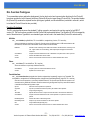
General Safety Precautions
Warning – High Voltages
The PhotoniQ Model IQSP584 interfaces to sensor interface boards (SIBs) through high voltage cable assemblies. The
PhotoniQ, SIB, and SIB power cable are energized with potentially harmful high voltages (up to 2000 Volts) during
operation.
Use Proper Power Source
The PhotoniQ Model IQSP584 is supplied with a +5V desktop power source. Use with any power source other than the
one supplied may result in damage to the product.
Operate Inputs within Specified Range
To avoid electric shock, fire hazard, or damage to the product, do not apply a voltage to any input outside of its specified
range.
Electrostatic Discharge Sensitive
Electrostatic discharges may result in damage to the PhotoniQ and SIB board set. Follow typical ESD precautions.
Do Not Operate in Wet or Damp Conditions
To avoid electric shock or damage to the product, do not operate in wet or damp conditions.
Do Not Operate in Explosive Atmosphere
To avoid injury or fire hazard, do not operate in an explosive atmosphere.
- 10 Vertilon Corporation, 66 Tadmuck Road, Westford, MA 01886 / Tel: (978) 692-7070 / Fax: (978) 692-7010 / www.vertilon.com
User Manual
Product Overview
The PhotoniQ Model IQSP584 is designed to offer scientists, engineers, and developers an off-the-shelf solution for their
multi-channel electro-optic sensor needs. Implemented as a stand-alone laboratory instrument with a PC interface, the
PhotoniQ is used for charge integration and data acquisition (DAQ) from photomultiplier tubes, photodiodes, silicon
photomultipliers, and other multi-element charge-based sensors. It is a precision, high speed, multi-channel parallel
system capable of providing real-time DSP-based signal processing on input events. Flexible intelligent triggering allows
the unit to reliably capture event data using one of several sophisticated triggering techniques. Two data acquisition
modes enable data collection of random events such as those found in particle analysis applications, or continuous
events from scanned imaging applications. Optional accessories such as dual on-board high voltage supplies are
available for applications requiring high voltage biasing. Through the PC, the PhotoniQ is fully configurable via its USB
2.0 port using an included graphical user interface. Continuous high speed data transfers to the PC are also handled
through this interface. Additionally, a LabVIEW™ generated DLL is provided for users who wish to write their own
applications that interface directly to the unit.
Features
•
128 gated integrator / data acquisition channels
•
14-bit dynamic range
•
Event pair resolution of 6.5 usec for 128 channels, 3.9 usec for 64 channels, and 2.5 usec for 32 channels
•
Maximum trigger rate of 140KHz for 128 channels, 250 KHz for 64 channels, and 385 KHz for 32 channels
•
Graphical User Interface (GUI) for menu driven data acquisition and configuration
•
GUI supports real time display of acquired data in linear and two dimensional graphs
•
Two data acquisition modes optimized for particle analysis and scanned imaging applications
•
Intelligent triggering firmware module supports standard edge, internal, level, and boxcar modes
•
Advanced triggering capability supports pre-triggering, input threshold, and cross bank
•
Flexible control of integration parameters such as delay, period, or external boxcar
•
Highly parallel, high speed hardware processor unit performs real-time data discrimination, channel gain
normalization and background subtraction
•
Programmable data filtering function for real time detection of predefined energy patterns or spectrums
•
General purpose digital output linked to filter function
•
Event trigger stamping and time stamping with 100 nsec resolution
•
USB 2.0 interface supports high data transfer rates
•
LabVIEW™ generated DLLs for interface to user custom applications
•
Available with up to two negative 1000V, negative 1500V, or negative 100V high voltage bias supplies
- 11 Vertilon Corporation, 66 Tadmuck Road, Westford, MA 01886 / Tel: (978) 692-7070 / Fax: (978) 692-7010 / www.vertilon.com
PhotoniQ IQSP584 128 Channel Data Acquisition System
Applications
Applications
1
Bioaerosol Detection and Discrimination
PET and SPECT
Fluorescence Spectroscopy
Spatial Radiation Detection
Confocal Microscopy
Piezoelectric Sensor Array Readout
Flow Cytometry
Particle Physics
DNA Sequencing
Arrays of Individual Sensors
Gamma Cameras
Silicon Photomultipliers (SPM)
Multi-Pixel Photon Counters(MPPC)
Compatible Sensors
1
Hamamatsu 32 Element Multianode PMT
P/N H7260
Hamamatsu 16 Element Multianode PMT
P/N H8711
Hamamatsu 16 Element Multianode PMT
P/N R5900U-L16
Hamamatsu 64 Element Multianode PMT
P/N H8500D
Hamamatsu 64 Element Multianode PMT
P/N H7546B
Photonis 64 Element Multianode MCP-PMT
P/N XP85013
SensL 16 Element Silicon Photomultiplier Array
P/N ArraySL-4
Hamamatsu 16 Element Multi-Pixel Photon Counter
P/N S11064
Pacific Silicon Sensor 16 Channel APD Array
P/N AD-LA-16-9-DIL18
Sensor Interface Boards available for specific sensors. Other sensor arrays can be accommodated. Contact Vertilon for additional information.
- 12 Vertilon Corporation, 66 Tadmuck Road, Westford, MA 01886 / Tel: (978) 692-7070 / Fax: (978) 692-7010 / www.vertilon.com
User Manual
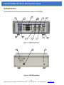
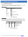
Hardware
The two photos below show the front and rear views of the PhotoniQ IQSP584
Figure 1: Model IQSP584 Front View
Figure 2: Model IQSP584 Rear View
(Shown with optional DIO100 digital I/O port)
- 13 Vertilon Corporation, 66 Tadmuck Road, Westford, MA 01886 / Tel: (978) 692-7070 / Fax: (978) 692-7010 / www.vertilon.com
PhotoniQ IQSP584 128 Channel Data Acquisition System
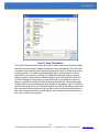
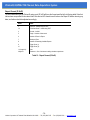
Software
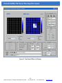
The screen shot below shows the main window of the Graphical User Interface (GUI) software included with the
PhotoniQ. All control, status, and acquisition functions are executed through this interface.
5
1
6
2
7
8
3
4
Figure 3: PhotoniQ Control and Acquisition Software Front Panel
1. Pull Down Menus
5. Status Indicators
2. Main Display Area
6. Counters & Event Data
3. Status Bars
7. Display Type
4. Acquire Button
8. Control Section
- 14 Vertilon Corporation, 66 Tadmuck Road, Westford, MA 01886 / Tel: (978) 692-7070 / Fax: (978) 692-7010 / www.vertilon.com
User Manual
Included Components and Software
The PhotoniQ comes enclosed in a rugged, EMI-shielded, laboratory instrument case and is shipped with the following
standard components and software:
•
PhotoniQ Control and Acquisition Interface Software CD-ROM
•
DC power supply (+5V, 2A) with power cord
•
USB 2.0 cable
Ordering Information
The PhotoniQ IQSP584 can be ordered with the following options pre-installed.
Option
Number
Option
Description
Notes
HVPS001
Negative 1000V on-board high voltage bias supply,
includes 90 cm high voltage cable (HVC090)
HVPS002
Negative 1500V on-board high voltage bias supply,
includes 90 cm high voltage cable (HVC090)
HVPS701
Negative 100V on-board high voltage bias supply,
includes 90 cm high voltage cable (HVC090)
MEM064
Memory upgrade, 250,000 event image buffer when
configured for 128 channels
500,000 events when configured for 64 channels
1,000,000 events when configured for 32 channels
MEM032
Memory upgrade, 125,000 event image buffer when
configured for 128 channels
250,000 events when configured for 64 channels
500,000 events when configured for 32 channels
DIO100
External digital data interface
Allows external digital data to be acquired in parallel
with the signal data
Up to two may be added in any combination
Table 1: Ordering Information (Configuration Options)
- 15 Vertilon Corporation, 66 Tadmuck Road, Westford, MA 01886 / Tel: (978) 692-7070 / Fax: (978) 692-7010 / www.vertilon.com
PhotoniQ IQSP584 128 Channel Data Acquisition System
Hardware Accessories
The following items are hardware accessories for the PhotoniQ IQSP584 that can be separately ordered. Typical
accessories include sensor interface boards and sensor interface board cables.
1
2
•
Sensor interface board for Hamamatsu S11064 16 element silicon photomultiplier (SIB416)
•
Sensor interface board for Hamamatsu R5900U-L16 PMT (SIB016)
•
Sensor interface board for Hamamatsu H8711 PMT (SIB116)
•
Sensor interface board for Hamamatsu H7260 series PMT (SIB232)
•
Sensor interface board for Hamamatsu H7260 series PMT, long integration times (SIB232D)
•
Sensor interface board for Hamamatsu H8500D series PMT (SIB064A)
•
Sensor interface board for Hamamatsu H7546B series PMT (SIB164A)
•
Sensor interface board for Photonis XP85013 series MCP-PMT (SIB264)
•
Sensor interface board for SensL ArraySL-4 16 element silicon photomultiplier (SIB1256)
•
Sensor interface board for PSS 1 AD-LA-16-9-DIL avalanche photodiode array (SIB216)
•
32 channel SMB distribution system (SDS232)
•
Sensor interface board cable, 30 cm, 60 cm, and 90 cm (SBC030, SBC060, SBC090)
•
Custom sensor interface board 2
Pacific Silicon Sensor, Inc.
Contact Vertilon for custom SIB design for sensors not listed.
- 16 Vertilon Corporation, 66 Tadmuck Road, Westford, MA 01886 / Tel: (978) 692-7070 / Fax: (978) 692-7010 / www.vertilon.com
User Manual
Specifications
(Typical specifications at room temperature)
System Specifications
Item
Value
Resolution
14 bits
Dynamic Range
84 dB
Equivalent Input Noise Charge
100 fC RMS typ.
Maximum Input Signal
Channel-to-Channel Crosstalk
Input Bias Current
Test Conditions
Edge triggered mode. Other modes slightly higher or lower.
877 pC
-84 dB typical, -80 dB max.
For integration periods greater than 300 nsec.
±40 pA typical, ±150 pA max.
Input Offset Voltage
±1.5 mV max.
Offset relative to input bias voltage which is 0.250V.
Power Consumption
10.0 Watts typ.,
12.0 Watts max.
Assumes no optional high voltage bias supplies. Add 0.7W
for each bias supply at max voltage and max load.
High Voltage Bias Supply Range (HVPS001)
-50 V to -925 V
At a load of 370 uA. Voltage range divided by three at SIB
(-17V to -308V) when using SIB216.
High Voltage Bias Supply Range (HVPS002)
-100 V to -1390 V
At a load of 250 uA.
High Voltage Bias Supply Range (HVPS701)
-5.0 V to -92.5 V
At a load of 1 mA.
Table 2: System Specifications
General Timing Specifications
Item
Configured Channels
Test Conditions
128
96
64
32
Maximum Trigger Rate (MTR)
140 KHz
180 KHz
250 KHz
385 KHz
MEM064 event buffer option installed and
image mode enabled. Integration period of 100
nsec.
Minimum Event Pair Resolution (MEPR)
Edge Trigger, Integration Time = 100 nsec
6.5 usec
5.1 usec
3.9 usec
2.5 usec
Minimum Event Pair Resolution (MEPR)
Pre Trigger, Integration Time = 1 x TS
7.5 usec
5.8 usec
4.1 usec
2.8 usec
Assumes 95% acquisition success with five
consecutive triggers spaced apart by MEPR
time.
Minimum Event Pair Resolution (MEPR)
Pre Trigger, Integration Time = 2 x TS
9.2 usec
8.3 usec
5.8 usec
3.5 usec
Sustained Average Event Rate (SAER)
22,000
30,000
45,000
75,000
Events per second. Specification assumes PC
and USB port capable of handling continuous
data transfers at ~16MB/sec and all log file
reporting functions disabled.
MEM064 Event Buffer Size (EBS)
250K
333K
500K
1M
MEM032 Event Buffer Size (EBS)
125K
167K
250K
500K
Measured in events consisting of all configured
channels. The standard unit does not include
an event buffer.
Table 3: General Timing Specifications
- 17 Vertilon Corporation, 66 Tadmuck Road, Westford, MA 01886 / Tel: (978) 692-7070 / Fax: (978) 692-7010 / www.vertilon.com
PhotoniQ IQSP584 128 Channel Data Acquisition System
Trigger and Integration Specifications 1
Description
Sym
Trigger/Mode
Minimum
Maximum
ttd
Edge
0 nsec
1 msec
ttd
Edge
tptd
Pre-trigger
Pre-Trigger Uncertainty
tptu
Pre-trigger
Integration Start Delay
tbcd1
Boxcar
Trigger to Integration Delay
Trigger to Integration Jitter
Pre-Trigger Delay
3
2
Integration Start Jitter
± 5 nsec
-10TS
+1000TS
TS
15 nsec
25 nsec
Boxcar
± 5 nsec
Integration End Delay
tbcd2
Boxcar
15 nsec
25 nsec
Boxcar Width Resolution
tbcw
Boxcar
Integration Period
tint
Edge
50 nsec
1000 msec
Internal
50 nsec
1000 msec
Level
50 nsec
1000 msec
Boxcar
50 nsec
1000 msec
Input
TS
1000TS
Pre-trigger
TS
1000TS
10 nsec
Integration Period Error
tint
All
Internal Trigger Rate
ftrig
Internal
10 Hz
200 KHz
Level
10 Hz
200 KHz
Input
59.5 fC
487 pC
Trigger Threshold Range
Sample Period
TS
±500 psec
1.67 usec. for
1.27 usec. for
0.87 usec. for
0.47 usec. for
128 channels
96 channels
64 channels
32 channels
1.67 usec. for
1.27 usec. for
0.87 usec. for
0.47 usec. for
128 channels
96 channels
64 channels
32 channels
Table 4: Trigger and Integration Specifications
1
2
3
Typical specifications at room temperature.
A fixed delay of approximately 15 nsec is in addition to the delay setting.
Relative to system sample period, TS. A negative value for the delay corresponds to a pre-trigger condition.
- 18 Vertilon Corporation, 66 Tadmuck Road, Westford, MA 01886 / Tel: (978) 692-7070 / Fax: (978) 692-7010 / www.vertilon.com
User Manual
Miscellaneous Specifications
Description
Sym
Minimum
Maximum
General Purpose ADC Input Range
ADC
0V
+3.0 V
General Purpose DAC Output Range
DAC
0V
+3.0 V
General Purpose SIB DAC Input Range
SIB DAC
0V
+3.0 V
Trigger Input Voltage Range
TRIG IN
0V
+3.3V, +5.0 V max.
Trigger Input Logic Low Threshold
TRIG IN
Trigger Input Logic High Threshold
TRIG IN
+4.2 V
Trigger Input, Input Impedance
TRIG IN
1 Mohm
Trigger Input, Rise Time
TRIG IN
Trigger Input, Positive Pulse Width
TRIG IN
100 nsec
Trigger Input, Negative Pulse Width
TRIG IN
100 nsec
Trigger Output Voltage Range
TRIG OUT
0V
+3.3V
General Purpose Output Voltage Range
AUX OUT
0V
+3.3V
General Purpose Output Delay
AUX OUT
100 nsec
2 msec
General Purpose Output Period
AUX OUT
100 nsec
2 msec
Trigger Stamp Counter Range
0
232-1
Time Stamp Counter Range
0
232-1
Time Stamp Resolution (Decade Steps)
100 nsec
1 msec
Time Stamp Maximum (Decade Steps)
429.4967 sec
49.71026 days
Event Counter Range
0
108
+0.8 V
20 nsec
Trigger to External Word DR High
tdr
1 usec
External Word SCK to SDO Valid
tdv
10 nsec
External Word SCK period
tsck
50 nsec
100 nsec
Table 5: Miscellaneous Specifications
Mechanical Specifications
Description
Specification
Width
9.843 in. (250 mm)
Height
3.346 in. (85 mm)
Depth
10.236 in. (260 mm)
Table 6: Mechanical Specifications
PC System Requirements
•
Microsoft Windows XP operating system
•
Intel USB 2.0 high-speed host controller with 82801Dx chipset (low speed is not supported)
•
Run-time engine for LabVIEW™ version 9.0 for use with DLL
- 19 Vertilon Corporation, 66 Tadmuck Road, Westford, MA 01886 / Tel: (978) 692-7070 / Fax: (978) 692-7010 / www.vertilon.com
PhotoniQ IQSP584 128 Channel Data Acquisition System
Typical PET Setup
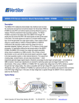
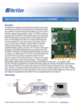
A typical setup for a PET scanner application using a Vertilon PhotoniQ IQSP584, two Vertilon SIB064’s, and two
Hamamatsu H8500D 8 x 8 multianode photomultiplier tubes is shown below. The 64 element MAPMTs are each
connected to a SIB064 and positioned to detect incoming light from a scintillator crystal or optical assembly. The four
sensor interface board cables (SIB cables) connect the 64 detector outputs from each SIB064 to the PhotoniQ 128
channel data acquisition system. High voltage bias to the MAPMTs is controlled by connecting the high voltage output on
the PhotoniQ front panel to the detector bias input on the SIB064. This arrangement allows the user to have a convenient
means to control the photomultiplier tube gain through the PhotoniQ GUI. In the example below, the two high voltage bias
outputs from the PhotoniQ are used so that the user has independent control over each MAPMT. The Pulse Detect
outputs from the SIB064s fire when an event exceeding a user-programmed energy threshold is detected. The external
coincidence detector measures the time between events and generates a trigger signal to the PhotoniQ if the events
occur within a predefined time interval. Digitized output data from the PhotoniQ is then sent to a PC over a USB 2.0
connection for display, logging, or real time processing.
Figure 4: Typical Setup for PET Scanner
- 20 Vertilon Corporation, 66 Tadmuck Road, Westford, MA 01886 / Tel: (978) 692-7070 / Fax: (978) 692-7010 / www.vertilon.com
User Manual
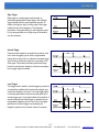
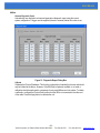
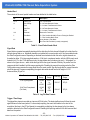
In a PET application, the PhotoniQ is configured in pre-trigger mode whereby the unit can capture the charge data from
the detectors that occurred prior to the trigger signal. This powerful triggering mode allows the data acquisition unit to be
timed to the pulse peaks or to high energy thresholds yet still collect all of the charge from the particle event — including
the charge that preceded the trigger. Timing for this mode is shown below.
INTEGRATION
AREA
EVENT
TRIGGER
WINDOW SET RELATIVE
TO TRIGGER POINT
AND MATCHES
EVENT PULSE WIDTH
TRIGGER
POINT
INTEGRATION
WINDOW
FINAL LEVEL
EQUALS TOTAL
ENERGY FROM
EVENT
CHARGE
SIGNAL
Figure 5: PhotoniQ Pre-Trigger Timing
- 21 Vertilon Corporation, 66 Tadmuck Road, Westford, MA 01886 / Tel: (978) 692-7070 / Fax: (978) 692-7010 / www.vertilon.com
PhotoniQ IQSP584 128 Channel Data Acquisition System
Theory of Operation
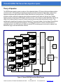
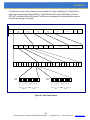
The IQSP584 data acquisition system is made up of four independent banks of 32 charge collection and data acquisition
circuits for a total of 128 simultaneous integrating and sampling channels. Each bank is independently configured and
triggered and generates eight parallel streams of digital data as shown in the figure below. The intelligent trigger/
acquisition module configures the triggering and acquisition parameters for each bank such that any one of multiple
triggering modes can be used to initiate the data acquisition process. A total of thirty-two parallel digital data channels are
output to the Pipelined Parallel Processor (P3) where it performs data channel offset and uniformity correction. Time
multiplexing the signals from the sampling channels allows the P3 to process the data in four time slices (Channel Blocks
1 through 4) so that all 128 channels are operated on. The resulting data from the P3 is sent to the DSP where it is
packetized and sent to the USB output port. Additional reserved DSP processing power can be used to implement user
defined filter, trigger, and data discrimination functions.
Block 4
Channels
Block 3
Channels
Block 2
Channels
Block 1
Channels
Channels 97-104
PROCESSOR
EXPANSION
INTERFACE
ADC
Channels 65-72
ADC
BANK1
Channels 33-40
ADC
BANK1
Channels 1-8
BANK 1
INPUTS
ADC
BANK1
Channels 105-112
ADC
BANK1
SDRAM
Channels 73-80
ADC
32 CHANNEL
PIPELINED
PARALLEL
PROCESSOR
BANK2
Channels 41-48
ADC
BANK2
Channels 9-16
BANK 2
INPUTS
ADC
BANK2
Channels 113-120
ADC
BANK2
Channels 81-88
ADC
BANK3
Channels 49-56
ADC
16-BIT
DIGITAL
SIGNAL
PROCESSOR
BANK3
Channels 17-24
BANK 3
INPUTS
ADC
BANK3
Channels 121-128
ADC
BANK3
Channels 89-96
ADC
BANK4
Channels 57-64
ADC
BANK4
Channels 25-32
BANK 4
INPUTS
ADC
BANK4
BANK4
INTELLIGENT
TRIGGER/
ACQUISITION
Figure 6: PhotoniQ IQSP584 Functional Block Diagram
- 22 Vertilon Corporation, 66 Tadmuck Road, Westford, MA 01886 / Tel: (978) 692-7070 / Fax: (978) 692-7010 / www.vertilon.com
USB
User Manual
Charge Collection & Data Acquisition Channels
Data acquisition is initiated by a trigger signal detected by the PhotoniQ’s intelligent trigger module. Each trigger starts
the collection and digitization of charge signals from the PMT, silicon photomultiplier, or photodiode sensors across all
channels. This functionality, which is shown in the previous figure as an amplifier followed by an ADC, is implemented
primarily as precision analog circuit elements that integrate, amplify, and digitize charge. The parallel architecture of this
circuitry allows charge integration and digitization to take place simultaneously across all channels thus achieving very
high data acquisition speeds. Additionally, the proprietary design of the front end preamp permits very narrow charge
pulses to be reliably captured with single photon sensitivity at very high repetition rates.
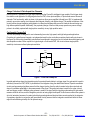
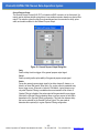
Configurable Preamp Cell
The front end preamp is designed for use in demanding low noise, high speed, and high background applications.
Consisting of a gated boxcar integrator, an independent reset function, and other proprietary functionality not shown in
the figure, the front end is dynamically controlled and reconfigured to support any one of several advanced triggering and
data acquisition modes. When coupled to a typical single or multi-anode PMT, this circuit achieves single photon
sensitivity at microsecond-level pulse-pair resolution.
RESET
GATE
ADC
+
BIAS
Figure 7: Front End Preamp Cell
In gated applications where the integration period is precisely timed relative to a trigger signal, the gate switch is used to
selectively connect the PMT, SiPM, or photodiode to the integrator during the desired time interval. Special cancellation
circuitry and processing algorithms ensure that the charge injection from the switch remains below the noise level and
does not contribute appreciably to the measurement of the signal. This gating technique is used for the edge, internal,
and level trigger modes. A different gating scheme is used for the input and pre-triggering modes where the gate switch
remains closed for all time, and the integration period is set using digital techniques. Under these conditions the system is
at risk of saturation because of constant optical background signals and electrical bias currents applied to the integrator.
A proprietary algorithm in conjunction with specialized circuitry ensures that the integrator remains well within its linear
region thus maintaining virtually all of its dynamic range.
- 23 Vertilon Corporation, 66 Tadmuck Road, Westford, MA 01886 / Tel: (978) 692-7070 / Fax: (978) 692-7010 / www.vertilon.com
PhotoniQ IQSP584 128 Channel Data Acquisition System
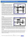
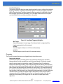
Pipelined Parallel Processor
The P3 Pipelined Parallel Processor shown on the next page is a dedicated high speed hardware processing unit that
executes 32 parallel channels of computations on the 32 data streams from the front-end digitizing blocks. Each channel
processor performs real-time data discrimination, buffering, and channel uniformity correction. Time division multiplexing
of the inputs to the P3 allows it to operate on all 128 channels of data in four time slices. The outputs from the 32 channel
processors are sent to the frame post processor where additional frame-formatted data manipulation is performed. The
frame post processor output is sent to the Parallel Peripheral Interface (PPI) where it is formatted and transferred to the
DSP for further processing.
PROCESSOR
EXPANSION
INTERFACE
PIPELINED SIGNAL PROCESSING CHANNELS 1-8
PULSE
DISCRIMINATOR
PRE-TRIGGER
BUFFER
UNIFORMITY
CORRECTION
CHANNEL
POST
PROCESSOR
FRAME
POST
PROCESSOR
PIPELINED SIGNAL PROCESSING CHANNELS 9-16
PULSE
DISCRIMINATOR
PRE-TRIGGER
BUFFER
UNIFORMITY
CORRECTION
CHANNEL
POST
PROCESSOR
PPI
32 x 4 TDM
CHANNELS
PIPELINED SIGNAL PROCESSING CHANNELS 17-24
PULSE
DISCRIMINATOR
PRE-TRIGGER
BUFFER
UNIFORMITY
CORRECTION
CHANNEL
POST
PROCESSOR
PIPELINED SIGNAL PROCESSING CHANNELS 25-32
PULSE
DISCRIMINATOR
PRE-TRIGGER
BUFFER
UNIFORMITY
CORRECTION
CHANNEL
POST
PROCESSOR
INTELLIGENT
TRIGGERING
Figure 8: 32-Channel Pipelined Parallel Processor
- 24 Vertilon Corporation, 66 Tadmuck Road, Westford, MA 01886 / Tel: (978) 692-7070 / Fax: (978) 692-7010 / www.vertilon.com
TO
DSP
User Manual
Digital Signal Processor
The 16 bit fixed point digital signal processor performs the high level data manipulation and system control in the
PhotoniQ. Channel data received from the P3 on the PPI is routed through the DSP and buffered using the on-board
SDRAM. This architecture allows the PhotoniQ to capture very large frames of data, such as the kind typically found in
imaging applications, without the loss of any data. Once the data is stored, it is packetized by the USB packet generator
and sent out to the PC through the USB 2.0 port. Extra computational power is reserved in the DSP so that user-defined
algorithms can be executed on the data prior to transmission. This has the benefit that routines that were previously
performed off-line by the PC can instead be handled in real-time. The net effect is that the downstream data load to the
PC is reduced so that throughput can be increased by orders of magnitude. In addition to user-defined filtering and
triggering functions, the DSP can be used to process commands from the PC and drive external actuators and devices.
EXTERNAL
ACTIVATORS
PPI
WATCH
DOG
TIMER
P3
CONFIGURATION
USER
PROGRAMMABLE
REAL-TIME
FRAME
PROCESSOR
USB
PACKET
GENERATOR
REAL
TIME
CLOCK
P3
IN-CIRCUIT
PROGRAM
USB
FIFO
USB
CONTROL
USB
COMMAND
PROCESSOR
DSP
IN-CIRCUIT
PROGRAM
INTERNAL/
EXTERNAL
I/O
Figure 9: DSP Functional Block Diagram
- 25 Vertilon Corporation, 66 Tadmuck Road, Westford, MA 01886 / Tel: (978) 692-7070 / Fax: (978) 692-7010 / www.vertilon.com
PhotoniQ IQSP584 128 Channel Data Acquisition System
Control and Acquisition Interface Software
The PhotoniQ is programmed and monitored by the Control and Acquisition Interface Software. This software, which is
resident on the PC, provides a convenient GUI to configure and monitor the operation of the unit. Configuration data used
to control various functions and variables within the PhotoniQ such as trigger and acquisition modes, integration time,
processing functions, etc. is input through this interface. For custom user applications, the GUI is bypassed and control
and acquisition is handled by the user’s software that calls the DLLs supplied with the PhotoniQ. As configuration data is
modified, the PhotoniQ’s local, volatile RAM memory is updated with new configuration data. The hardware operates
based upon the configuration data stored in its local RAM memory. If power is removed from the PhotoniQ, the
configuration data must be reprogrammed through the GUI. However, a configuration can be saved within the non-volatile
flash memory of the PhotoniQ. At power-up, the hardware loads configuration data from its flash memory into its volatile
RAM memory. Alternatively, the RAM memory can be configured from a file on the user’s PC.
Intelligent Triggering and Integration
One of the most powerful features of the PhotoniQ is the wide variety of ways the data acquisition process can be
triggered. The unit consists of an intelligent trigger module with the capability to trigger the input channels in conventional
external or internal post trigger modes. Additionally, advanced on-board signal processing techniques permit more
sophisticated triggering modes such as pre-trigger, which captures events that occur prior to the trigger signal, and input
trigger, which captures events based on a threshold criteria for the event. The PhotoniQ also has a cross bank triggering
mode that permits certain trigger parameters for each bank to be independently configured and operated. The
descriptions below illustrate some of the advanced trigger and integration capabilities of the PhotoniQ.
FRONT-END
TIMING
GENERATOR
EDGE
TRIGGER
INTERNAL
TRIGGER
LEVEL
TRIGGER
BOXCAR
GATE
TRIGGER/
ACQUISITION
PROCESSOR
P3
TIMING
GENERATOR
INPUT
TRIGGER
DSP
TIMING
GENERATOR
PRETRIGGER
TRIGGER
CONFIGURATION
TIMING
CONFIGURATION
Figure 10: Intelligent Trigger Module
- 26 Vertilon Corporation, 66 Tadmuck Road, Westford, MA 01886 / Tel: (978) 692-7070 / Fax: (978) 692-7010 / www.vertilon.com
User Manual
Edge Trigger
Edge trigger is a simple trigger mode whereby an
externally-supplied positive signal edge to the intelligent
trigger module starts the event acquisition process. As
shown in the figure at right, the rising edge of the trigger
initiates the start of the integration. The integration
parameters of integration delay (ttd) and integration period
(tint) are programmable over a large range of values with
very fine resolution.
Internal Trigger
Continuous data acquisition is possible by operation of the
unit in internal triggering mode. Here a programmable
internal free running clock (tclk) replaces the external trigger
signal. Data is continuously acquired on each edge of the
clock signal. This mode is particularly useful when large
blocks of event data are needed for collection and analysis,
but no trigger signal is available.
Level Trigger
This trigger mode is similar to internal triggering except that
an externally provided positive level-sensitive trigger gate
controls the acquisition of events. The actual trigger signal
is internally generated but synchronized and gated by the
external trigger gate. A logic high enables the acquisition of
events by allowing the internal trigger to generate the preprogrammed integration period. A logic low on the trigger
gate blocks the internal trigger from generating the
integration period so that no further events are acquired.
- 27 Vertilon Corporation, 66 Tadmuck Road, Westford, MA 01886 / Tel: (978) 692-7070 / Fax: (978) 692-7010 / www.vertilon.com
PhotoniQ IQSP584 128 Channel Data Acquisition System
Input Trigger
Input trigger is used to trigger the acquisition process
when incoming data on a specific channel exceeds a
user defined threshold. No external trigger signal is
required. The integration period determines the time over
which the input signal is integrated and is typically set to
closely match the expected pulse width. The figure shows
a timing diagram for input triggering. When using this
mode, the integration period must always be a multiple of
the sample period, TS. The charge integrated during the
integration time is compared to the trigger threshold level.
In the example, tint equals 3TS and event ‘A’ exceeds the
threshold and event ‘B’ does not. The crossing of the
threshold triggers the PhotoniQ to acquire data across all
channels. To better position the integration window
around the detected pulse, the actual window can be shifted by an integer number of TS intervals (positive delay only)
relative to when the threshold was crossed. In the example below, the integration window shift is one TS interval.
Pre-Trigger
In pre-trigger mode, an external positive edge sensitive
trigger signal is used to acquire event data that occurred
prior to the trigger’s arrival. As shown below, the
programmable pre-trigger delay (tptd) is used to set the
start of the programmable integration period (Tint) at a
time prior to the trigger edge. The pre-trigger uncertainty
time (tptu), shown as the dashed area in the figure, is
equal to sampling period of the system, TS. While the
start of the integration period is uncertain by time TS, the
actual duration of the integration period itself is quite
accurate. Both the pre-trigger delay and the integration
period are constrained to be multiples of the system’s
sampling period. The trigger output signal is a reference signal that can be used to setup the system. Regardless of the
pre-trigger delay time, the leading edge of the trigger out always occurs between 0 and TS from the leading edge of the
trigger input signal. The period of the trigger out is precisely equal to the integration time. When the pre-trigger delay is
set to one (positive) TS, the start of the integration period precedes the rising edge of the trigger output by one half of
sample period, TS. For other pre-trigger delay times (either positive or negative), the actual integration window is shifted
accordingly.
Although pre-triggering mode is mostly used in applications where the integration window precedes the trigger edge (i.e.
when the pre-trigger delay is negative), positive pre-trigger delays are also permissible. This positive delay mode has
slightly lower noise than the edge trigger mode and can be used when precise control over the start (and end) of the
integration period is not necessary.
- 28 Vertilon Corporation, 66 Tadmuck Road, Westford, MA 01886 / Tel: (978) 692-7070 / Fax: (978) 692-7010 / www.vertilon.com
User Manual
Cross Bank Triggering
The flexibility of the PhotoniQ allows one or more channel banks to be triggered with one set of parameters which in turn
trigger other banks using a different set of parameters. In a typical example, a bank is set up as an input trigger type with
a particular integration period. The other banks are set up with different delays and integration periods. When an input
event crosses the specified threshold on the first bank, the other banks can then be triggered. Data acquisition on these
banks occurs with their respective specified delays and integration periods. The figure at right illustrates this example.
Bank 1 is the main trigger bank and is setup as an input trigger type with an integration period of Tint1 and integration
delay of zero. Trigger timing for Bank 2 and Bank 3 is setup independently from Bank1. The integration delay for these
banks is Td2 and Td3, respectively, and the integration period is Tint2 and Tint3, respectively. For simplicity, Bank 4 is not
shown. The main trigger point occurs when the signal on Bank 1 crosses the defined input threshold. From that point,
Bank 2 and Bank 3 trigger after their defined integration delay time has elapsed. Each independently integrates over its
defined integration period.
Integration Delay and Period
The integration delay is the parameter that sets the start of the integration period relative to the rising edge of the trigger.
Only for pre-triggering can this value be negative. The integration period is the time duration over which the input signal is
accumulated in the charge sensitive preamp. Both integration parameters are adjustable.
Boxcar Mode
Boxcar mode utilizes the input trigger signal to set the two
integration parameters. The preset values are ignored. As
shown in the figure, the trigger signal is used to define the
period over which the input is to be integrated. Aside from a
small amount of fixed positive delay (times tbcd1 and tbcd2),
the boxcar formed by the trigger signal is the integration
period (tbcw) and any unwanted background signals that
occur when the boxcar is inactive are not integrated and
effectively masked out.
Boxcar Width
The PhotoniQ has the ability to determine the width of the boxcar input signal. For each triggering event, the system
measures the width of the boxcar and appends it to the event data in the log file if enabled. This feature is particularly
useful for particle sizing where the boxcar is generated from threshold crossings on an external scatter channel. The
sizing information (boxcar width) could then be used to normalize the spectral data.
- 29 Vertilon Corporation, 66 Tadmuck Road, Westford, MA 01886 / Tel: (978) 692-7070 / Fax: (978) 692-7010 / www.vertilon.com
PhotoniQ IQSP584 128 Channel Data Acquisition System
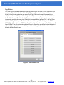
Hardware Interface
The photos below show the front and rear panel interface connectors on the IQSP584.
11
2
10
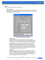
13
8
12
4
5
3
1
9
7
6
Figure 11: IQSP584 Front Panel
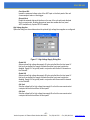
14
15
16
Figure 12: IQSP584 Rear Panel
- 30 Vertilon Corporation, 66 Tadmuck Road, Westford, MA 01886 / Tel: (978) 692-7070 / Fax: (978) 692-7010 / www.vertilon.com
User Manual
1. Main Power Switch: PhotoniQ main power switch.
2. Sensor Interface Board Connectors (SIB Connectors): Connectors to SIB cables for
connection to a sensor interface board or signal distribution system. Each connector and
cable carries 32 input channels over individual coaxial lines. Additional control and monitor
lines are also carried.
3. Trigger Input (BNC): Main trigger input to the PhotoniQ. This input is positive edge
sensitive.
4. Trigger Indicator (Green LED): Indicates when a trigger is supplied to the PhotoniQ on the
Trigger Input connector.
5. Trigger Output (BNC): Main trigger output from the PhotoniQ. When in edge or internal
trigger mode, the output from this connector is the integration window used by the PhotoniQ
to integrate the signal. If cross bank triggering is enabled, this output is the integration
window from the main trigger bank(s). There are no trigger outputs associated with the
secondary bank(s). In input trigger and pre-trigger modes, the trigger output indicates the
trigger point shifted by the programmable delay time.
6. Auxiliary Output (BNC): Configurable general purpose output.
7. Acquisition Indicator (Green LED): Indicates when an event is acquired by the PhotoniQ.
8. ADC Input (BNC): Input to the internal analog to digital converter.
9. DAC Output (BNC): Output from the internal digital to analog converter.
10. High Voltage Bias Supply #1 Output (SHV): Cable connector for the optional high voltage
bias supply #1 (HV1).
11. High Voltage Bias Supply #1 Indicator (Yellow LED): Indicates when the optional high
voltage bias supply #1 (HV1) is energized.
12. High Voltage Bias Supply #2 Output (SHV): Cable connector for the optional high voltage
bias supply #2 (HV2).
13. High Voltage Bias Supply #2 Indicator (Yellow LED): Indicates when the optional high
voltage bias supply #1 (HV2) is energized.
14. External Word Interface (10-Pin IDC): Optional digital I/O interface for external word.
15. USB Cable Input (USB B Type): USB cable connection to PC.
16. Main Power Input (2mm Barrel): +5V input from external power supply.
- 31 Vertilon Corporation, 66 Tadmuck Road, Westford, MA 01886 / Tel: (978) 692-7070 / Fax: (978) 692-7010 / www.vertilon.com
PhotoniQ IQSP584 128 Channel Data Acquisition System
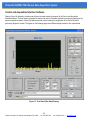
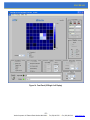
Control and Acquisition Interface Software
Running Control & Acquisition Interface.exe will open the main window (front panel) of the Control and Acquisition
Interface Software. The front panel is generally for display and control of the data acquisition process and reporting of the
system’s operational status. Various pull-down menus are used for setting the configuration of the PhotoniQ and for
performing diagnostic routines. The figures on the following pages show different display modes for the acquired data.
Figure 13: Front Panel (Bar Graph Display)
- 32 Vertilon Corporation, 66 Tadmuck Road, Westford, MA 01886 / Tel: (978) 692-7070 / Fax: (978) 692-7010 / www.vertilon.com
User Manual
Figure 14: Front Panel (2D Single 8 x 8 Display)
- 33 Vertilon Corporation, 66 Tadmuck Road, Westford, MA 01886 / Tel: (978) 692-7070 / Fax: (978) 692-7010 / www.vertilon.com
PhotoniQ IQSP584 128 Channel Data Acquisition System
Figure 15: Front Panel (2D Dual 8 x 8 Display)
- 34 Vertilon Corporation, 66 Tadmuck Road, Westford, MA 01886 / Tel: (978) 692-7070 / Fax: (978) 692-7010 / www.vertilon.com
User Manual
Control Area
This area allows the user to define the acquisition, triggering, and integration parameters and control system settings.
Acquisition
The Control and Acquisition Interface Software supports four types of acquisition modes for real time display
and/or logging of event data from the PhotoniQ hardware. A fifth acquisition mode allows the user to view a
logged file in the display area.
Display Only
This mode is intended for use in setting up the user’s system when the real time impact of
modifications is needed, such as during optical alignment or detector bias adjustment. Most of
the front panel functions are accessible. Data is collected from the PhotoniQ one event at a time
and displayed in the display area in the GUI. Additional trigger events are ignored until the
display is completely updated. The processing overhead necessary to display the data greatly
reduces the maximum event capture rate.
Display & Log
Similar to the Display Only mode except that the user is able to log the viewed events. The
display overhead severely reduces the maximum event rate that can be logged without a loss of
data. Most of the front panel functions are disabled in this mode.
Particle
In this mode data from the PhotoniQ is logged directly to a file. With the exception of the Event
and Trigger counters, the display and front panel functions are disabled so that the maximum
achievable logging rate can be attained. Data acquisition is optimized for the collection of
stochastic events. Triggers to the PhotoniQ are not accepted if the system is busy processing an
event that was previously acquired. The uniform acquisition process makes this mode well suited
for particle analysis applications. The maximum data acquisition rate will vary depending upon
the user’s computer system.
Image
Data acquisition is optimized for the rapid collection of events over a predefined period of time.
Generally used in scanned imaging applications, this mode allows the PhotoniQ to be triggered
at the highest rate possible. Data is stored in an image buffer where it is then logged at a slower
speed to the PC. In a typical application, the PhotoniQ is triggered at the pixel clock rate and the
image size, buffer size, and timing is configured such that the system can capture and store a full
scan of the subject image before logging the data to the PC.
Log File View
Allows the user to select a previously logged file for viewing in the display area. Events are
stepped-through using the event index box.
Acquire (Select File) Button
Toggles between Acquire and Standby for display and logging acquisition modes. Once a
configuration has been set, the user starts acquiring data by toggling this switch to Acquire.
When the Log File View acquisition mode is selected, this button allows the user to select the log
file for viewing. Pushing the button opens a dialog box through which a data file can be selected
for manual playback.
- 35 Vertilon Corporation, 66 Tadmuck Road, Westford, MA 01886 / Tel: (978) 692-7070 / Fax: (978) 692-7010 / www.vertilon.com
PhotoniQ IQSP584 128 Channel Data Acquisition System
Log Path
Indicates the location of the data file that has been selected for logging or viewing.
Status Line
Status information and error messages regarding the PhotoniQ’s operation are displayed in this
box. The LED is green under normal conditions and turns red when there is an error condition.
Processing
Allows the user to select which processing functions, if any, are applied to the data. The parameters for the
individual processing functions are entered in their respective dialog boxes which can be found under the
Processing pull-down menu.
Background Subtraction
Enables subtraction of a pre-calculated background signal from the total signal.
Gain Compensation
Enables gain compensation of channel to channel non-uniformities.
Spectral Filtering
Enables the spectral filtering processor.
2D Filtering
Enables the two dimensional filtering processor.
System
Used to set and monitor the PhotoniQ hardware peripherals. The high voltage functions are available only if the
high voltage bias supply options are installed and activated in the High Voltage Supply dialog box found under
the System pull down menu.
HV1 On
Enables high voltage bias supply #1. This function is available only if high voltage bias supply #1
is enabled under the High Voltage Supply dialog box.
HV1 Set Point
Sets the output voltage of high voltage bias supply #1. Cannot exceed upper limit set under High
Voltage Supply dialog box.
HV2 On
Enables high voltage bias supply #2. This function is available only if high voltage bias supply #2
is enabled under the High Voltage Supply dialog box.
HV2 Set Point
Sets the output voltage of high voltage bias supply #2. Cannot exceed upper limit set under High
Voltage Supply dialog box.
Front Panel DAC
Sets the output voltage of the front panel general purpose digital to analog converter.
SIB DAC
Sets the output voltage of the digital to analog converter on the sensor interface board
connector. This function is typically used to control precision discriminator threshold signals on
specialized sensor interface boards.
- 36 Vertilon Corporation, 66 Tadmuck Road, Westford, MA 01886 / Tel: (978) 692-7070 / Fax: (978) 692-7010 / www.vertilon.com
User Manual
Integration
Sets the signal integration parameters for the acquisition process.
Integration Delay
Used with Edge, Input, and Pre-trigger types, this parameter sets the delay from the trigger
source to the start of the integration period. Negative values are permitted if Pre-trigger is
selected as the trigger type. This parameter is ignored when Boxcar mode is enabled.
Integration Period
Used with all trigger types, this parameter sets the duration of the integration period. For Input
and Pre-trigger, the period minimum is equal to the PhotoniQ sample period – a parameter that
is dependent on the speed configuration of the PhotoniQ. When using Input or Pre-trigger, only
integer multiples of the PhotoniQ sample period can be used as the Integration Period. This
parameter is ignored when Boxcar mode is enabled.
Boxcar
Available only with Edge trigger type, Boxcar mode uses the externally supplied trigger signal to
set the integration delay and integration period. The preset integration parameters are ignored.
The integration period starts immediately after the rising edge of the user supplied boxcar trigger
signal. The integration period equals the width of the boxcar signal.
Boxcar Width
Displays the width of the boxcar input. To enable this feature, Boxcar mode must be selected in
the front panel and the Boxcar Width box must be checked in the Data Configuration menu.
Trigger
Sets the trigger parameters for the acquisition process.
Type
Used to select the trigger type of Edge, Internal, Level, Input, or Pre-trigger. For Edge, Level and
Pre-trigger types, the user supplies the trigger signal (positive edge/level) to the trigger input
BNC connector on the PhotoniQ. For Internal trigger type, the PhotoniQ supplies the internal
trigger and therefore no external input is required. Input triggering does not require a trigger
signal but does require setting a threshold level.
Rate
Used in conjunction with Internal and Level trigger types. This parameter sets the rate of the
internally generated trigger signal.
Threshold
Sets the charge threshold level for Input triggering.
Channel
Sets the channel number used for Input triggering.
Cross Bank Enable
When cross bank triggering is disabled, the front panel’s trigger and integration parameters are
applied identically to all four banks of channels. In this configuration, the PhotoniQ is triggered
once and data is collected across all channels simultaneously using the front panel settings for
the integration delay and period. When cross bank triggering is enabled, different integration
delays and integration periods are applied to each bank of channels. In this configuration, the
front panel trigger parameters are applied to the main trigger bank(s). The settings for the
secondary banks are configured under the Cross Bank Trigger configuration menu.
- 37 Vertilon Corporation, 66 Tadmuck Road, Westford, MA 01886 / Tel: (978) 692-7070 / Fax: (978) 692-7010 / www.vertilon.com
PhotoniQ IQSP584 128 Channel Data Acquisition System
Event Data
Displays real time event specific data.
Filter Match
This function is active when the data filter processing is enabled. It indicates when a particular
event matches the filter criteria.
Out of Range
Indicates when one or more channels in a displayed event are out of range.
Input Error
Indicates when an input error has been detected on one or more channels in a displayed event.
Certain types of input overloads can cause an input error condition.
Trigger Count
This indicator keeps count of the absolute number of triggers seen by the system since the
beginning of the Acquire period. The counter is reset at the start of the Acquire period and
effectively counts all triggers (regardless of whether a trigger was accepted or rejected) until the
Acquire period ends. In Image acquisition mode, the Trigger Count is used as a system status
indicator that shows the current number of pixels counted by the PhotoniQ. It also serves as a
diagnostic tool to ensure that the maximum trigger rate to the PhotoniQ is not exceeded. If the
Trigger Count equals the Event Count after the acquired data has been transferred to the PC,
then no pixels were missed. The Trigger Count is also valuable in Particle acquisition mode
where it can be compared to the Event Count to determine the percentage of events acquired by
the PhotoniQ. Note that if the event rate is exceptionally high, the displayed Trigger Count will
slightly lag the actual trigger count measured by the system. It is also important to note that
unlike Particle and Image mode where the displayed Trigger Count will be equal to the Trigger
End Count at the end of the acquisition period, this will usually not be the case when using the
Display and Display & Log modes. Although the system in these modes will accurately count the
triggers and stop when the Trigger End Count is reached, the final displayed Trigger Count will
only indicate the number of triggers counted when the last event was acquired. The additional
triggers are counted to reach the Trigger End Count but not displayed because none of them
resulted in the acquisition of an event.
Trigger End Count
A user programmable value that specifies the Trigger Count value that terminates the Acquire
period. This is normally used in Image acquisition mode where it is set equal to the total number
of pixels in the scanned image. In this way, the PhotoniQ acquires a complete image in its event
buffer, ends its acquisition period, and transfers the buffered data to the PC. A value of zero for
the Trigger End Count corresponds to an infinite acquisition period.
Event Count
Indicates the running total of the number of events accepted by the PhotoniQ and transferred to
the PC. The counter is cleared when an acquisition period is restarted and will roll over if the
maximum event total is reached. This counter is also used as an indicator of the total number of
events in a log file when in Log File View mode. The Event Count and Trigger Count are the only
two indicators active when in Particle or Image acquisition mode. Note, when the PhotoniQ is in
the Display Only or Display & Log acquisition modes, the Event Count will usually be much less
than the Trigger Count because the overhead from the real time data display significantly slows
the event acquisition rate. The Particle and Image acquisition modes, on the other hand, are high
speed data acquisition modes that are able to keep up with the trigger rate provided it is within
- 38 Vertilon Corporation, 66 Tadmuck Road, Westford, MA 01886 / Tel: (978) 692-7070 / Fax: (978) 692-7010 / www.vertilon.com
User Manual
the specified limits. Under these conditions, the Event Count will usually equal Trigger Count
after the acquisition period ends and all events are transferred to the PC. However, even in these
two high speed modes it is possible for the Event Count to be less than the Trigger Count. This
can occur if the trigger specification is exceeded—even momentarily—or if the Acquire button is
pressed while active triggers are input to the system. To avoid the latter situation, the Acquire
button should be pressed before any triggers are applied to the system.
Event Index
Available only in Log File View mode, this box allows the user to scroll through events or to enter
a specific event number for viewing from the log file. The maximum event index is equal to the
event total.
Front Panel ADC
Displays the value in volts measured on the PhotoniQ front panel general purpose ADC input.
The input is sampled each time the unit is triggered. Sampling occurs coincident with the rising
edge of the trigger input signal and is independent of the integration and delay time parameters.
Data will be displayed in this area even if the Front Panel ADC is left unchecked in the Data
Configuration menu because the system will update the value even if no trigger is applied.
Enabling the Front Panel ADC in the Data Configuration menu will insert the ADC sample
associated with each trigger in the event packet in the log file. When used, this input should be
driven by a low impedance device.
External Word
When enabled in the Data Configuration menu this field displays the 16-bit value (in decimal) of
the externally generated data word. The external word is transferred to the PhotoniQ through the
digital interface connector located on the rear of the unit. The interface is designed to serially
shift-in a 16-bit digital word immediately after an external trigger is applied to the system. If the
trigger signal is accepted by the PhotoniQ and an event created, the external word
corresponding to the accepted trigger signal is displayed on the front panel if in Display or
Display & Log Mode. It is also appended to the event data packet.
Trigger/Time Stamp
Shows the trigger or time stamp for the event currently displayed in the display window. The
trigger stamp is the running total of all triggers seen by the system since the start of the Acquire
period. Time stamps are taken in fixed resolution steps as determined in the Data File
Configuration pull-down menu and are also referenced to the start of the Acquire period. The
Trigger/Time Stamp counter rolls over after the maximum value is reached. To enable this
feature the Trigger/Time Stamp must be selected in the Data Configuration menu.
Display
Configures the real time display area.
Source
Selects the type of data plotted on the display. The logged data and processing functions are
unaffected by this selection.
Signal
The input signal is plotted on the real time display. If Background Subtraction is
enabled, the raw input signal minus the background is displayed.
- 39 Vertilon Corporation, 66 Tadmuck Road, Westford, MA 01886 / Tel: (978) 692-7070 / Fax: (978) 692-7010 / www.vertilon.com
PhotoniQ IQSP584 128 Channel Data Acquisition System
Background
Only the pre-calculated background signal is plotted on the real time display.
Select this display function when initially configuring the system to minimize the
background optical signal. This function is only available if Background
Subtraction processing is enabled.
Display Type
The display type for the input channels is selected using this feature. Different sized bar and two
dimensional intensity graphs can be used to display the input signal data.
Bar
Displays a single linear bar graph with the signal channels on the x-axis and their
corresponding signal amplitude in picocoulombs on the y-axis. The number of
channels for display can be 32, 64, or 128 channels. The channel mapping for the
graph is selected directly beneath the graph in a separate dropdown selection
box.
2-D
Displays a two dimensional (x-y) intensity graph of the signal channels with the
signal amplitude in picocoulombs displayed as intensity. The graph choices
consist of a dual 4 x 4 display, single 8 x 8, or dual 8 x 8. The channel mapping for
the graphs is selected directly beneath them in separate dropdown selection
box(es).
- 40 Vertilon Corporation, 66 Tadmuck Road, Westford, MA 01886 / Tel: (978) 692-7070 / Fax: (978) 692-7010 / www.vertilon.com
User Manual
Real Time Display Area
The display area is used to give a graphical view of the data collected while in the Display Only and Display & Log
acquire modes. For these modes the displayed data is obtained directly from the PhotoniQ in real time. Data is also
shown in the display area when viewing a previously logged file in Log File View mode. The display area and its
associated control functions are disabled when either Particle or Image is selected as the acquisition mode.
Display
Displays the real time signal in picocoulombs (pC) from each of the input channels. Data is also shown on the
display when viewing a previously logged file in Log File View mode. The signal data can be displayed as a
single bar graph, single two-dimensional intensity map, or dual two-dimensional intensity map.
Display Limit Adjust
Clicking the upper or lower vertical scale value allows the display limits to be adjusted.
Channels
Selects the channel range for display.
Flip X
Inverts the x-axis for 2D displays.
Flip Y
Inverts the y-axis for 2D displays.
Transpose
Swaps the x-axis and y-axis for 2D displays.
- 41 Vertilon Corporation, 66 Tadmuck Road, Westford, MA 01886 / Tel: (978) 692-7070 / Fax: (978) 692-7010 / www.vertilon.com
PhotoniQ IQSP584 128 Channel Data Acquisition System
Pull Down Menus
The pull down menus are available at the top of the graphical user interface window.
File
File operations generally consist of storing and retrieving PhotoniQ configurations between the PC and the
PhotoniQ’s volatile and non-volatile (flash) memory. Configuration information stored in volatile memory will be
lost when power to the PhotoniQ is removed. The default configuration will be loaded on power up.
Configuration information stored in flash memory will be retained even when power to the PhotoniQ is removed.
New
Loads the PhotoniQ with the default configuration.
Open
Loads the PhotoniQ with a stored configuration from a file on the PC.
Save
Saves the current configuration of the PhotoniQ to a file on the PC.
Save As
Saves the current configuration of the PhotoniQ to a new file on the PC.
Read from Flash
Loads the PhotoniQ with the configuration stored in the PhotoniQ’s flash memory.
Write to Flash
Writes the current configuration of the PhotoniQ to its flash memory
Print Window
Prints the current window.
Exit
Closes the executable.
- 42 Vertilon Corporation, 66 Tadmuck Road, Westford, MA 01886 / Tel: (978) 692-7070 / Fax: (978) 692-7010 / www.vertilon.com
User Manual
System
The PhotoniQ is configured through this pull down menu.
Data Configuration
Opens the dialog box shown below where the PhotoniQ log file settings are configured. The log
file will increase in size when any of these items are selected. See section on Log Files for the
specifics on the log file sizes and format.
Figure 16: Data Configuration Dialog Box
Enabled Channels
Configures the number of input channels used by the system which in-turn
determines the size of the output data packets. Channels are arranged by banks
with 32 channels per bank. The number of channels per bank also determines the
operating speed of the unit. If any bank is configured with 25 or more channels,
the IQSP584 timing operates like a 128 channel system — regardless of the
configuration of the other banks. Similarly, if the maximum number of channels in
any bank is between 17 and 24, then the unit’s timing behaves like a 96 channel
unit. If all banks are configured with 8 or less channels, then the PhotoniQ speed
is maximized and operates like a 32 channel unit.
Input Polarity
Changes the polarity of the input preamplifiers on the PhotoniQ. Normally set to
positive, this configuration switch is used to match the preamplifier’s polarity to the
direction of the current from the sensor attached to the sensor interface board
connector. The PhotoniQ should be recalibrated if this switch is changed. See the
sensor interface board’s user manual for more details.
- 43 Vertilon Corporation, 66 Tadmuck Road, Westford, MA 01886 / Tel: (978) 692-7070 / Fax: (978) 692-7010 / www.vertilon.com
PhotoniQ IQSP584 128 Channel Data Acquisition System
Data Format
The data format for the signal data in the log file can be configured in either of two
ways; 17-bit Sign-Magnitude or 16-bit Two’s Complement. The 17-bit option
inserts the magnitude of the channel data into 16-bit words and “bit-packs” the
sign bits for each channel into additional sign words. For a 128 channel
configuration this format adds 16 extra words to the event packet. While in most
applications it is possible to ignore the sign bit and assume the data is always
positive, there are occasions when the sign bit is important such as in system
noise characterization. The 16-bit format does not append additional sign words to
the events in the log file. Signal data is simply inserted into 16-bit words in a
standard two’s complement representation.
Range Bits
Inserts out of range (OOR) and input error (ERR) data for each channel into the
log file. The range data is reported for each event. Out of range occurs when the
input signals are too large (negative or positive) for the electronics. An input error
is reported when a fault other than an out of range is detected. Regardless of
whether this option is selected, the header for each event contains data to indicate
if at least one of the channels in the event packet is out of range or has an input
error.
Trigger / Time Stamp
Inserts a two word trigger or time stamp for each event into the log file. The
selection choices are Trigger, Time (100nsec), Time (1 usec), Time (10 usec),
Time (100 usec), Time (1 msec), and Off. No trigger or time stamp is inserted into
the log file if Off is selected.
The Trigger option inserts the absolute count of the number of triggers seen by the
system for each event that is acquired. The trigger stamp is reset to zero at the
start of Acquire mode. Ideally, in a scanned imaging application, the trigger stamp
will increment by exactly one for each event (pixel). An increment of greater than
one indicates that one or more triggers were missed. This usually indicates that
the trigger rate exceeded the maximum trigger rate for the system. In a particle
application, the trigger stamp can be used as a measure of the percentage of
particles missed by the system.
The five Time options are used to insert a time stamp with a programmable
resolution from 100 nsec to 1 msec. Like the trigger stamp, the time stamp is reset
to zero at the start of Acquire mode. To obtain absolute time, an absolute time
stamp — taken when the PhotoniQ first enters Acquire mode and inserted into the
header at the top of each log file — can be added to the relative time stamps
appended to each event. Time stamping is most useful in particle analysis
applications where particle interarrival times can be measured. Although not as
useful in imaging applications, the time stamp can function as a good diagnostic
tool if trigger frequency or scan time needs to be measured.
Boxcar Width
Inserts the measured width of the external boxcar signal for each event into the
log file.
- 44 Vertilon Corporation, 66 Tadmuck Road, Westford, MA 01886 / Tel: (978) 692-7070 / Fax: (978) 692-7010 / www.vertilon.com
User Manual
Front Panel ADC
Inserts the measured voltage value of the ADC input on the front panel of the unit.
A new sample is taken on each trigger.
External Word
Enable the external data word interface on the rear of the unit and inserts the data
into the event packet. Enabling the external word also enables the front panel
ADC. Available only if option DIO100 installed.
High Voltage Supplies
Opens the dialog box shown below where the optional high voltage bias supplies are configured.
Figure 17: High Voltage Supply Dialog Box
Enable HV1
Allows optional high voltage bias supply #1 to be controlled from the front panel. If
this box is unchecked, the supply is turned off and the front panel controls are
disabled. Supply HV1 is typically used in conjunction with the first 64 channels on
the PhotoniQ.
Enable HV2
Allows optional high voltage bias supply #2 to be controlled from the front panel. If
this box is unchecked, the supply is turned off and the front panel controls are
disabled. Supply HV2 is typically used in conjunction with the second 64 channels
on the PhotoniQ.
HV1 Limit
Sets the voltage limit for high voltage bias supply #1 so that the user cannot select
a set point above this level from the front panel.
HV2 Limit
Sets the voltage limit for high voltage bias supply #2 so that the user cannot select
a set point above this level from the front panel.
- 45 Vertilon Corporation, 66 Tadmuck Road, Westford, MA 01886 / Tel: (978) 692-7070 / Fax: (978) 692-7010 / www.vertilon.com
PhotoniQ IQSP584 128 Channel Data Acquisition System
General Purpose Output
The General Purpose Output (AUX OUT) is located on a BNC connector on the front panel. It is
mainly used in real-time particle sorting where it can enable an actuator based on a spectral filter
match. This selection opens the dialog box shown below where the user sets the delay, pulse
width, and enable condition for the General Purpose Output.
Figure 18: General Purpose Output Dialog Box
Delay
Sets the delay time from trigger of the general purpose output signal.
Period
Sets the period (positive pulse width) of the general purpose output signal.
Enable
Forces the general purpose output signal to be either always off, always on, or
linked to an event filter match. When set to On, a pulse output is generated every
time a trigger occurs. When set to Linked to Filter Match, a pulse output occurs
only when Spectral Filtering is enabled and an event meets the filter criteria. If
Spectral Filtering is disabled, the pulse output will be generated for every trigger.
Note that the Spectral Filtering operation takes a non-zero amount of time that is
dependent on the Spectral Filtering configuration. This limits the minimum delay
that can be selected for the General Purpose Output. The user needs to
determine this empirically for a given Spectral Filtering configuration.
- 46 Vertilon Corporation, 66 Tadmuck Road, Westford, MA 01886 / Tel: (978) 692-7070 / Fax: (978) 692-7010 / www.vertilon.com
User Manual
Cross Bank Triggering
This selection opens the dialog box shown below that allows the user to configure the cross bank
triggering parameters. Triggering of the secondary banks occurs after the triggering of the main
bank(s). Secondary banks are always triggered as Edge type where the trigger edge is derived
from the trigger output from the main bank(s). The Cross Bank Enable box on the front panel
must be checked for the cross bank parameters to be applied.
Figure 19: Cross Bank Triggering Dialog Box
Main Trigger
Selects the bank(s) for the main trigger. Each selected bank is configured with the
triggering parameters from the front panel.
Int Delay
Sets the integration delay for each of the secondary bank(s).
Int Period
Sets the integration period for each of the secondary bank(s).
Processing
The PhotoniQ processing functions are configured through this pull down menu.
Background Subtraction
The PhotoniQ includes a processing function that continuously subtracts a pre-calculated
background level from the raw signal from each of the input channels. This function is useful
when the raw input signal is dominated by a stable DC background level. By enabling the
Background Subtraction processing, a DC background signal is removed from each channel for
each event so that only the actual desired signal can be displayed or logged. Pressing the Apply
button performs the background level computation on each channel. The computed values are
then used for the Background Subtraction processing if enabled. Calculation of the background
level should be initiated anytime the user changes the system parameters. Note that Background
Subtraction does not increase the dynamic range of the system nor does it remove the shot
noise associated with the background. Its main use is to improve the display of the data and
simplify the post processing of the logged data. It is also useful for optical system setup
diagnostics.
- 47 Vertilon Corporation, 66 Tadmuck Road, Westford, MA 01886 / Tel: (978) 692-7070 / Fax: (978) 692-7010 / www.vertilon.com
PhotoniQ IQSP584 128 Channel Data Acquisition System
Gain Compensation
Gain compensation processing allows the user to normalize the outputs from the individual
channels of a particular sensor. This is helpful when compensating for channel-to-channel
responsivity differences in multi-anode PMTs and photodiode arrays. The gain compensation
dialog box shown in Figure 20 lets the user adjust each channel by a positive or negative
percentage. For example, a positive 2% adjustment into a specific channel will effectively
multiply the raw data for that channel by 1.02. A negative 2% adjustment would multiply the raw
data by 0.98. The compensation coefficient range is -100% to +100%. The coefficients default to
0 % when gain compensation is disabled.
Figure 20: Gain Compensation Dialog Box
Spectral Filtering
Spectral Filtering is used to selectively display, log, or tag events that meet a specific user
defined matching criteria. It is typically used in fluorescence detection or other applications where
the acquired event data represents spectral or wavelength information. Spectral filtering is
described in more detail in the Data Filtering section.
2D Filtering
2D Filtering is used to selectively display, log, or tag events that meet a specific user defined
matching criteria. It is most appropriate for applications such as PET and particle physics that
use position sensitive detectors. 2D filtering is described in more detail in the Data Filtering
section.
- 48 Vertilon Corporation, 66 Tadmuck Road, Westford, MA 01886 / Tel: (978) 692-7070 / Fax: (978) 692-7010 / www.vertilon.com
User Manual
Utilities
Generate Diagnostic Report
Automatically runs diagnostic routines and generates a diagnostic report using the current
system configuration. A trigger must be supplied (internal or external) before this routine is run.
Figure 21: Diagnostic Report Dialog Box
Calibrate
Calibrates the PhotoniQ hardware. This function is generally not intended for the user and should
only be initiated at the factory. However, if the SIB cable is replaced, modified, or not used, a
calibration should be performed to compensate for any small differences in the cables. To initiate
a calibration, configure the PhotoniQ and confirm that the SIB is not connected to the other end
of the cable. Press the Apply button to calibrate the unit.
- 49 Vertilon Corporation, 66 Tadmuck Road, Westford, MA 01886 / Tel: (978) 692-7070 / Fax: (978) 692-7010 / www.vertilon.com
PhotoniQ IQSP584 128 Channel Data Acquisition System
Log File Converter
This utility converts the binary files (.log) created during logging into tab delimited text files (.txt).
The readable text files can be used as is or imported into a database program for further
processing. For details on the data format of binary and text log files, the Log Files section of this
manual should be consulted.
When the Log File Converter utility is selected, the dialog box shown in Figure 22 opens. Here
the user selects the source binary file (.log) that is to be converted into a text file (.txt) by
pressing the Select File button. This in turn opens the dialog box shown in Figure 23 where the
user then browses to the source file. The target file is the name of the text file that results from
the conversion of the source binary file. Similar in behavior to the source file select button, a
dialog box opens where the user browses to the target directory and names the target file. Once
both the source and target files are selected, the converter is initiated by pressing the Convert
button. The progress of the log file conversion process is monitored by observing the Progress
bar at the top of the dialog box.
Figure 22: Log File Converter Dialog Box
- 50 Vertilon Corporation, 66 Tadmuck Road, Westford, MA 01886 / Tel: (978) 692-7070 / Fax: (978) 692-7010 / www.vertilon.com
User Manual
Figure 23: Select File Dialog Box
The Log File Converter can also process binary files in a batch mode to save time when multiple
binary files are to be converted. Instead of browsing for a source file when the Select File button
is pressed, the user selects an entire directory by pressing the Select Cur Dir button as shown in
the dialog box above. This effectively selects all binary files (i.e. all files ending in .log) in the
source directory for conversion to text files. The target Select File button opens up a similar
dialog box where the user selects the destination directory for the text files with the Select Cur
Dir button. Pressing the Convert button converts all files with the .log extension in the source
directory, and places the resulting text files into the destination directory. The target file names
are identical to the source names except the file extension is changed from .log to .txt. Note that
since the batch mode of the Log File Converter attempts to convert all files ending in .log into text
files, care should be taken to ensure that all .log files in the source directory are valid binary log
files. If the converter encounters an invalid binary file, the conversion process will abort and no
files, valid or invalid, will be converted.
- 51 Vertilon Corporation, 66 Tadmuck Road, Westford, MA 01886 / Tel: (978) 692-7070 / Fax: (978) 692-7010 / www.vertilon.com
PhotoniQ IQSP584 128 Channel Data Acquisition System
Data Filtering
When either the Spectral Filtering or 2D Filtering processing function is enabled, an output marker can be generated for
each event that meets a predefined filter criteria. If the result is true, a positive going digital pulse is output on the General
Purpose Output connector (AUX OUT) on the front panel of the PhotoniQ. The timing for this pulse is configured under
the General Purpose Output pull down menu. In addition to the marker pulse, events in the log file are tagged so that
those that meet the filter criteria can be identified when subsequently displayed or analyzed. To minimize the data
processing load to the host processor, a Block Data Transmission configuration switch is available to block events that do
not meet the filter criteria from being logged or displayed. When this switch is set, only data that generates a true
response to the filter criteria is transmitted. Note, since spectral and 2D filtering are real-time embedded DSP functions in
the PhotoniQ, a reduction in the maximum data acquisition rate can be expected when either of these functions are
enabled.
Spectral Filtering
Spectral filtering is most useful in applications where the acquired data represents wavelength or frequency
information. It is also possible to use it in one dimensional, linear positional applications. Typically the spectral
filter is configured to accept or reject events that meet a predefined criteria or discriminant. For instance, the
filter can be setup to acquire events that match a particular fluorescence spectral pattern and reject all others.
Parameters for the filter are entered in three tabbed panes in the dialog box under the Spectral Filtering option
in the Processing menu. The data filtering processor operates on spectral bands defined by the user in the
Band Definition pane according to a Boolean expression defined in the Flag Definition and Discriminant
Definition panes.
- 52 Vertilon Corporation, 66 Tadmuck Road, Westford, MA 01886 / Tel: (978) 692-7070 / Fax: (978) 692-7010 / www.vertilon.com
User Manual
Band Definition
The Band Definition pane allows the user to create a set of up to eight frequency or position bands that are used
to compare spectral or location regions, respectively. A band is defined as a continuous sequence of channels.
For example, in the figure below Band 1 is defined as channels 3 through 5 and Band 2 as channels 6 through
7. Bands 3 through 8 are not defined. It is not necessary to define all bands. However, care should be taken to
not include unused channels in a band definition or unused bands in the Flag Definition described on the next
page.
Figure 24: Band Definition Pane
- 53 Vertilon Corporation, 66 Tadmuck Road, Westford, MA 01886 / Tel: (978) 692-7070 / Fax: (978) 692-7010 / www.vertilon.com
PhotoniQ IQSP584 128 Channel Data Acquisition System
Flag Definition
Up to eight flags can be defined by the user in the Flag Definition pane. The result of a flag computation on the
spectral or position data is either true or false. All eight flags have the same structure in which the operand on
the left is tested for being greater than the operand on the right. Within each operand, the user selects a
multiplier and either a constant (equal to the weight of one LSB) or the average of one of the bands defined in
the Band Definition pane. This allows the data filter processor to compare a band to a constant or compare two
independently scaled bands to each other. Referring to the example below, two flags (Flag 1 and Flag 2) are
defined in the Flag Definition pane. Flag 1 is true if one times the average of Band 1 is greater than 60 times
0.0595 pC (the LSB weight for an IQSP584) and Flag 2 is true if one times the average of Band 2 is less than 70
times 0.0595 pC. The data discriminator operates on these two flags with a user defined function to determine if
a filter match occurred. Note the user should only use bands in the flag definitions that have been enabled and
defined in the Band Definition pane.
Figure 25: Flag Definition Pane
- 54 Vertilon Corporation, 66 Tadmuck Road, Westford, MA 01886 / Tel: (978) 692-7070 / Fax: (978) 692-7010 / www.vertilon.com
User Manual
Discriminant Definition
The data filter match function is programmed in the Discriminant Definition pane as a logical combination of the
previously defined flags utilizing a sum of products format. Each row in the table is a grouping of flags that are
logically AND’d together. The rows are then logically OR’d to produce the filter result. The Filter Criteria line
shows the resulting equation with “*” representing a logical AND and “+” representing a logical OR. Each event
can thus generate only a true or false condition. The user should only use flags in the discriminant definition that
have been defined and enabled in the Flag Definition pane. Checking the Block Data Transmission box in the
Discriminant Definition pane forces event data that generates a false response to the filter criteria to be blocked
from being logged or displayed. The output marker pulse is unaffected by the setting of this configuration switch.
Figure 26: Discriminant Definition Pane
With the product term definition shown above, the data filter function will generate a match only if the average of
channels 3, 4, and 5 is greater than 3.57 pC and the average of channels 6 and 7 is less than 4.17 pC. The
events that meet this criterion will have their corresponding data filter match bit set in the log file. However,
because the Block Data Transmission box is not checked, all events will be logged, regardless of the match
condition.
- 55 Vertilon Corporation, 66 Tadmuck Road, Westford, MA 01886 / Tel: (978) 692-7070 / Fax: (978) 692-7010 / www.vertilon.com
PhotoniQ IQSP584 128 Channel Data Acquisition System
2D Filtering
Filtering of two dimensional data from position sensitive devices is performed using the 2D filtering function.
The 2D filter is most effective in applications where single particles are detected based on their locations in the
detector array. In particle physics applications the detection criteria would be based on the energy level of the
particle. The 2D filtering parameters are entered in a single dialog box under the 2D Filtering option in the
Processing menu. The data filtering processor operates on a subsection of the detector array by comparing the
particle’s energy level to a predefined threshold or to another coincident particle’s energy level.
2D Filtering Definition
The 2D filter works by defining either one or two small filter areas in the detector array for comparison. Selection
areas are defined by first selecting the display mode as either a dual 4 x 4 or dual 8 x 8 matrix. The Channels
dropdown menu below each array is used to select which channels are assigned to each matrix. This defines
the Matrix A and Matrix B selection areas. Within these areas, the user clicks on the location of the filter areas,
which depending on the Filter Matrix size, can be either 1 x 1 or 2 x 2 pixels. Under the Enabled Flags A
location, the comparison condition flag is configured for Matrix A. For a 1 x 1 Filter Matrix, this condition is
applied to the single pixel defined in the display matrix. For a 2 x 2 Filter Matrix, the condition is independently
applied to each of the four pixels defined in the display area and, depending on the A Product Terms selection,
the conditions are either AND’d or OR’d together to produce a single Boolean result. The flag for Matrix B is
similarly configured under the Enabled Flags B location. The final filter criteria is determined by combining (by
ANDing or ORing) the Matrix A and Matrix B conditions using the A/B Product Term.
Figure 27: 2D Filtering Definition Pane
- 56 Vertilon Corporation, 66 Tadmuck Road, Westford, MA 01886 / Tel: (978) 692-7070 / Fax: (978) 692-7010 / www.vertilon.com
User Manual
Log Files
The Control and Acquisition Interface Software produces binary log files during data collection that can be viewed using
the GUI display or processed off-line for more thorough data analysis. The GUI display function is accessed using the
Log File View on the front panel. This acquisition mode allows the user to step through and view individual events in the
binary log file. More advanced data processing functions such as sorting and pattern detection can be applied by
operating directly on the binary log files or by using spreadsheet-based routines on text log files. If text file format is
desired, a function included with the Control and Acquisition Interface Software is used to convert the binary log files to
text log files.
Binary Log File Format
Binary log files are used to minimize the time required to transfer the data from the PhotoniQ to a hard disk on a PC. To
reduce processing overhead and storage requirements, it is recommended that any off-line data manipulations operate
on this type of file. The contents of the binary log files written by the Control and Acquisition Interface Software can be
broken into three main sections; the identification text header, the configuration table, and the data block. The ID Text
Header defined in Table 7 below is a simple header that identifies the PhotoniQ model number, date, time (24 hour
format), and version information. It is organized along 8-bit byte boundaries.
Offset (Bytes)
Description
Length (Bytes)
Contents
0
Product ID
17
"Vertilon xxxxxx[CR][LF]"
17
Date/Time String
19
"MM/DD/YY HH:MM xx[CR][LF]"
36
Software UI Version
28
"LabVIEW UI Version xxxxxxx[CR][LF]"
Table 7: Binary Log File (ID Text Header Section)
The Config Table section shown in Table 8 contains configuration information relating to the PhotoniQ hardware and
firmware. Unlike the ID Text Header section, the Config Table section is organized as 16-bit words instead of 8-bit bytes.
The configuration data is partitioned into three tables; user, custom, and factory. The user table contains the configuration
of the PhotoniQ set by the user through the user interface. Any custom configuration data is stored in the custom table.
Factory-programmed, read-only configuration data is found in the factory table.
Offset (Words)
Description
Length (Words)
Contents
32
Config Table Revision
1
1st 8 bits = Major Rev,
2nd 8 bits = Minor Rev
33
User Config Table
1000
User Configuration Binary Data
1033
Custom Config Table
250
Custom Configuration Binary Data
1283
Factory Config Table
750
Factory Configuration Binary Data
Table 8: Binary Log File (Config Table Section)
- 57 Vertilon Corporation, 66 Tadmuck Road, Westford, MA 01886 / Tel: (978) 692-7070 / Fax: (978) 692-7010 / www.vertilon.com
PhotoniQ IQSP584 128 Channel Data Acquisition System
The Data Block section defined in Table 9 below is made up of packets that contain event data. An event packet contains
the data for each channel and is created for each event that is acquired while logging. The length (L) of the event packets
is dependent on the configuration settings selected in the user interface. Packet data is partitioned along 16-bit word
boundaries.
Offset (Words)
Description
Length (Words)
Contents
2033
Data Packet # 1
L
First Event Packet
2033 +L
Data Packet # 2
L
Second Event Packet
…
…
L
…
2033 +(n+0)*L
Data Packet # n+1
L
nth+1 Event Packet
2033 +(n+1)*L
Data Packet # n+2
L
nth+2 Event Packet
2033 +(n+2)*L
Data Packet # n+3
L
nth+3 Event Packet
…
…
…
…
Table 9: Binary Log File (Data Block Section)
Event Packet Description
Format
Each event processed by the PhotoniQ IQSP584 generates an event packet of length, L, where L is in 16-bit
words. The packet consists of a single word header followed by signal data words containing the signal
information for each channel in the unit. Depending on the system configuration, there may be additional footer
words following the signal data that hold the trigger/time stamp, boxcar width, general purpose ADC sample, and
external data word.
When configured for 128 channels the IQSP584 produces 160 signal data words (128 words with sign and
range reporting off). Other channel configurations produce less signal data words as shown in the table below.
# of Configured Channels
# of Signal Data Words
(Sign & Range Words On)
# of Signal Data Words
(Sign & Range Words Off)
128
160
128
96
120
96
64
80
64
32
40
32
Table 10: Event Packet Signal Data Word Totals
- 58 Vertilon Corporation, 66 Tadmuck Road, Westford, MA 01886 / Tel: (978) 692-7070 / Fax: (978) 692-7010 / www.vertilon.com
User Manual
The figure below shows a generic example of an event packet for a system configured with 17-bit data format
(sign words on) and reporting for Range Bits (R), Trigger/Time Stamp (TS), Boxcar Width (BW), Front Panel
ADC (ADC), and External Word (EW) enabled. The numbers in parentheses in the figure indicate the number of
words for each data type in the packet.
HEADER
(1)
CH1 – CH32
(40)
BANK1
CH1 – CH8
CH33 – CH64
(40)
BANK2
CH9 – CH16
BANK3
CH17 – CH24
BANK4
CH25 – CH32
CH CH CH CH CH CH CH CH
1
2
3
4
5
6
7
8
SIGN
BITS
CH65 – CH96
(40)
BANK1
CH33 – CH40
S
R
15 14 13 12 11 10 9 8 7 6 5 4 3 2 1 0
CH97 – CH128
(40)
BANK2
CH41 – CH48
CH
9
BANK3
CH49 – CH56
...
CH
16
UNUSED
BANK4
CH57 – CH64
S
RANGE
BITS
C C C C C C C C C C C C C C C C
H H H H H H H H H H H H H H H H
8 7 6 5 4 3 2 1 8 7 6 5 4 3 2 1
TS
(2)
R
BW
(2)
ADC
(1)
BANK1 … BANK 4
CH65 – CH96
CH
17
...
CH
24
S
EW
(1)
BANK1 … BANK 4
CH97 – CH128
R
CH
25
...
CH
32
S
R
15 14 13 12 11 10 9 8 7 6 5 4 3 2 1 0
C C C C C C C C C C C C C C C C
H H H H H H H H H H H H H H H H
8 7 6 5 4 3 2 1 8 7 6 5 4 3 2 1
SIGN
OOR
ERR
Figure 28: Event Packet Format
- 59 Vertilon Corporation, 66 Tadmuck Road, Westford, MA 01886 / Tel: (978) 692-7070 / Fax: (978) 692-7010 / www.vertilon.com
PhotoniQ IQSP584 128 Channel Data Acquisition System
Header Word
The contents of the event packet header word are detailed in the table below.
Bit
Function
Description
15-13
Packet Type
’100’ = Event Packet
12
Out of Range
Fault
’0’ = No Faults Detected in Packet
’1’ = At Least 1 Fault Detected in Packet
11
Input Error
Fault
’0’ = No Faults Detected in Packet
’1’ = At Least 1 Fault Detected in Packet
10-6
Reserved
Reserved for Future Use
5
Filter Match
’0’ = Filter Condition Not Met for Event or Filtering Not Enabled
’1’ = Filter Condition Met for Event
4-0
Filter Match
Library Number
Library Number of Filter Match
Don’t Care if No Filter Match (currently unsupported)
Table 11: Event Packet Header Word
Signal Data
Signal data is organized sequentially starting with the data from the first channel followed by the data from the
second channel and so on. Individual channels are included in the event packet only if they are enabled under
the Data Configuration menu. Depending on the data format selected under this menu, signal channels are
formatted as either 17-bit sign-magnitude words or 16-bit two’s complement words; with the LSB for each word
located in bit 0. For the 17-bit data format only, the signal data also includes a sign word — “bit-packed” as
shown in the figure above — which holds the sign bits for the signal channels. Similarly “bit-packed” are the
range words that if enabled, hold the range reporting bits. Disabling the range bit reporting under the Data
Configuration menu removes the range words from the event packet. Sign and range bits for unused channels
should be ignored. Programs manipulating the signal data words should use the bit weight of 41.20
femtocoulombs (fC) per bit.
Data Format
Dec Data
Range
Hex Data
Range
LSB Wgt
Full Scale
Range
17-bit Sign-Magnitude
+16,383
to
-16,383
0 3FFF
to
1 3FFF
59.51 fC
877 pC
+16,383
to
-16,384
3FFF
to
C000
59.51 fC
877 pC
16-bit Two’s Complement
(Full Scale)
Table 12: Log File Data Formats
Trigger / Time Stamp
The trigger/time stamp is encoded as a two word (32-bit) value. The least significant word follows the most
significant word in the event packet. For time stamp reporting, the event time relative to the start of the
acquisition (the time in the ID Text Header) is computed by multiplying the time stamp by the time stamp
resolution selected in the Data Configuration menu. Disabling the reporting enable for this field removes that
data from the packet.
- 60 Vertilon Corporation, 66 Tadmuck Road, Westford, MA 01886 / Tel: (978) 692-7070 / Fax: (978) 692-7010 / www.vertilon.com
User Manual
Boxcar Width
The boxcar width is reported using two words. It is computed by multiplying the two-word, 32-bit boxcar value by
10 nanoseconds. Disabling the reporting enable for this field in the Data Configuration menu removes that data
from the packet.
Front Panel ADC
A single 16-bit word is used to report the measured value from the front panel, 12-bit analog-to-digital converter.
To convert the integer value found in the event packet into a voltage, the value is multiplied by 5 volts and
divided by 4096. Disabling the Front Panel ADC in the Data Configuration menu removes the data from the
event packet.
External Word
The external data word taken from the digital interface on the rear panel of the PhotoniQ is reported in this field
as a single 16-bit word. Disabling the External Word in the Data Configuration menu removes it from the event
packet. The DIO100 option is required for this function.
Packet Length
The length (L) in words of each packet is given by the generic equation:
L = 1+ (NC1+NC2+NC3+NC4) + (K1+K2+K3+K4)⋅(F+R) + 2⋅TS + 2⋅BW + ADC + EW
The settings include the Number of Channels in each bank (NC1to NC4) and the Data Format (F) which indicates
whether sign words are used or not. The 17-bit data format uses sign words (F=1), the 16-bit format does not
(F=0). Packet length is also dependent on the settings for the reporting enables for the Range Bits (R),
Trigger/Time Stamp (TS), Boxcar Width (BW), Front Panel ADC (ADC), and External Word (EW). The reporting
enables are set in the Data Configuration menu and can be either ‘1’ or a ‘0’. The value (Km) in the length
formula is an integer that is computed from the Number of Channels in bank m (NCm) by the equation:
Km = INT
NCm + 7
8
Minimum Packet Length
In certain applications it is desirable to minimize the size of the event packet so that the highest throughput to
the PC can be attained. Additionally, a reduced event packet size allows the PhotoniQ’s event buffer to hold
more events before the possibility of overflow. In a scanned imaging application this means that larger image
sizes or higher scan rates can be accommodated. The minimum event packet size is achieved by disabling all
reporting functions and selecting the 16-bit data format. Since the header word cannot be disabled, the resulting
event packet size is 33 words (66 bytes) for a 32 channel configuration, 65 words (130 bytes) for 64 channels,
97 words (194 bytes) for 96 channels, and 129 words (258 bytes) for 128 channels.
- 61 Vertilon Corporation, 66 Tadmuck Road, Westford, MA 01886 / Tel: (978) 692-7070 / Fax: (978) 692-7010 / www.vertilon.com
PhotoniQ IQSP584 128 Channel Data Acquisition System
Converting a Binary Log File to Text
Text log files should be used if a user wishes to import logged event data into a spreadsheet for further processing. A
built in routine is included in the GUI for the purpose of converting a binary log file (.log extension) into a text file (.txt
extension). The output of this conversion is a file containing a time and date stamp header and the logged event data
organized by row where each row represents a successive event. The event rows are stored as tab-delimited numbers
where the columns represent from left to right, Packet Number (#), Packet Type (PT), Out of Range (OR), Input Error
(IE), Filter Match (FM), and channels 1 through N in picocoulombs. Only configured channels appear in the log file —
unused channels are left out. If enabled, the Trigger/Time Stamp (TS), Boxcar Width (BW), Front Panel ADC Value
(ADC) and External Data Word (EW) are stored in the last four columns, respectively. A ‘4’ in the Packet Type column
indicates an event row — other packet types are currently unsupported. An out of range condition on any of the N data
channels is identified in the Out of Range column by a ‘1’. Input errors are similarly reported in the Input Error column. If
range bit reporting was enabled during logging, the individual channel data columns will contain the value “MAX” or “MIN”
depending on whether the signal was out of range high or low, respectively. An input error on a particular channel is
identified by the value “ERR” in its respective column in the table. The Filter Match column contains a ‘1’ when the event
met the filter criteria or a ‘0’ when it did not. If filter processing is not enabled this column is filled with ‘0’. Due to
conversion speed limitations, the log file converter should be used on files containing less than 20,000 events. Larger
files will take a noticeable time to process.
- 62 Vertilon Corporation, 66 Tadmuck Road, Westford, MA 01886 / Tel: (978) 692-7070 / Fax: (978) 692-7010 / www.vertilon.com
User Manual
Configuration Tables
The hardware and software configuration of the PhotoniQ is stored in three separate tables; user, custom, and factory
configuration tables. The sections that follow summarize the contents of the three tables. Some configuration parameters
are not used in certain PhotoniQ products. Additionally, parameter limits may differ depending on PhotoniQ model
number.
User Configuration Table
The user table contains the configuration of the PhotoniQ set by the user through the user interface. It is 1000 words long
and is described in the table below.
Index
Parameter Name
Type
Description
Parameter Limits
0
SystemMode
16 SHORT
Indicates current system mode, acquire or
standby mode
0 = Standby Mode
1 = Acquire Mode
1
HVLimit0
16 SHORT
Maximum allowed voltage on HV supply 1
Range = 100 – 13900 (10 – 1390V)
2
HVLimit1
16 SHORT
Maximum allowed voltage on HV supply 2
Range = 100 – 13900 (10 – 1390V)
3
NumChannelsB0
16 SHORT
Number of channels enabled bank 1
Range = 0 – 64
4
NumChannelsB1
16 SHORT
Number of channels enabled bank 2
Range = 0 – 64
5
NumChannelsB2
16 SHORT
Number of channels enabled bank 3
Range = 0 – 64
6
NumChannelsB3
16 SHORT
Number of channels enabled bank 4
Range = 0 – 64
7
HVEnabled
16 SHORT
Enables for high voltage supplies
Bit 0 = HV Supply 1 Enable/Disable
Bit 1 = HV Supply 2 Enable/Disable
8
HVSetpoint0
16 SHORT
Current setpoint HV supply 1 (DAC 6)
Range = 100 – 13900 (10 – 1390V)
9
HVSetpoint1
16 SHORT
Current setpoint HV supply 2 (DAC 7)
Range = 100 – 13900 (10 – 1390V)
10
UserConfigID
16 SHORT
Unused
N/A (0 – 65535)
11
DCRD_AOut_0
16 SHORT
Daughtercard analog out control (DAC 8)
0-4095 (3.0V full scale)
12
BandEnables
16 SHORT
Spectral filtering band enables
Range = 0 – 255 (each bit position
corresponds to 1 of 8 band enables)
13
Band0StartIndex
16 SHORT
Start index for spectral filtering band 1
Range = 0 – 255 (1 channel per bit)
14
Band0EndIndex
16 SHORT
End index for spectral filtering band 1
Range = 0 – 255 (1 channel per bit)
15-28
Band Indices for
Remaining Bands
16 SHORT
Start index for spectral filtering band 2 - 8
End index for spectral filtering band 2 - 8
Range = 0 – 255 (1 channel per bit)
29
FlagEnables
16 SHORT
Spectral filtering flag enables
Range = 0 – 255 (each bit position
corresponds to a flag enable)
30-33
Flag0Operand0Flag0Operand3
16 SHORT
Spectral filtering operands for flag 1
configuration
Flag0Operand0,2
Range = 0 – 32767
Flag0Operand1,3
Range = 0 – 7 or 65535
(1 channel per bit or LSB wgt, 65535)
34-37
Flag1Operand0Flag1Operand3
16 SHORT
Spectral filtering operands for flag 2
configuration
Same as Above
38-41
Flag2Operand0Flag2Operand3
16 SHORT
Spectral filtering operands for flag 3
configuration
Same as Above
- 63 Vertilon Corporation, 66 Tadmuck Road, Westford, MA 01886 / Tel: (978) 692-7070 / Fax: (978) 692-7010 / www.vertilon.com
PhotoniQ IQSP584 128 Channel Data Acquisition System
Index
Parameter Name
Type
Description
Parameter Limits
42-45
Flag3Operand0Flag3Operand3
16 SHORT
Spectral filtering operands for flag 4
configuration
Same as Above
46-49
Flag4Operand0Flag4Operand3
16 SHORT
Spectral filtering operands for flag 5
configuration
Same as Above
50-53
Flag5Operand0Flag5Operand3
16 SHORT
Spectral filtering operands for flag 6
configuration
Same as Above
54-57
Flag6Operand0Flag6Operand3
16 SHORT
Spectral filtering operands for flag 7
configuration
Same as Above
58-61
Flag7Operand0Flag7Operand3
16 SHORT
Spectral filtering operands for flag 8
configuration
Same as Above
62-69
PTerm0-PTerm7
16 SHORT
Spectral filtering product terms
Range = 0 – 255 (each bit position
corresponds to a flag)
70
DataFilterEnable
16 SHORT
Spectral filtering data filter blocks data
output if there is no spectral filter match
0 = Disabled
1 = Enabled
71
ProcessingEnables
16 SHORT
Enables for various signal processing
options
Bit 0 = Spectral Filtering Enable
Bit 1 = Gain Enable
Bit 2 = Background Subtraction Enable
72
TimestampEnable
16 SHORT
Enables/Disables timestamp output
0 = Disabled
1 = Enabled
73
DAC_Spare
16 SHORT
SIB analog out control (DAC 5)
0-4095 (3.0V full scale)
74-75
TimestampInterval
32 LONG
Timestamp interval configuration
Range = 10 – 100000 (10ns per bit)
76
CustomWordsEnable
16 SHORT
Enables/Disable custom words output
0 = Disabled
1 = Enabled
77
EventCustomCount
16 SHORT
Number of custom words
Range = 0 – 64 (1 word per bit)
78
RESERVED
16 SHORT
Unused
N/A (0 – 65535)
79
ImageAcqMode
16 SHORT
Image Acquisition Mode Enable
0 = Particle
1 = Image
80
InputTrigThresh
16 SHORT
Input trigger threshold
Range = 1 – 8191
81
InputTrigChannel
16 SHORT
Input trigger current channel
Range = 0 – 256 (1 channel per bit)
82
RangeErrorEnable
16 SHORT
Enables/Disables range and error output
0 = Disabled
1 = Enabled
83
CrossBankConfig
16 SHORT
Current cross-bank configuration
Bit 0 = Cross Bank Enable
Bit 1 = Bank 1 Main Trigger
Bit 2 = Bank 2 Main Trigger
Bit 3 = Bank 3 Main Trigger
Bit 4 = Bank 4 Main Trigger
84
ReportPackingMode
16 SHORT
Indicates high speed or real-time
acquisition
0 = Real-Time Acquisition (no packing)
1 = High Speed Acquisition
85
GPOutputEnable
16 SHORT
Enables/Disables general purpose output
0 = GP Output Disabled
1 = GP Output Always On
2 = GP Output Linked to Spectral
Filter Match
86-87
GPOutputDelay
32 LONG
General purpose output delay
Range = 10 – 200000 (0.1 – 2000us)
- 64 Vertilon Corporation, 66 Tadmuck Road, Westford, MA 01886 / Tel: (978) 692-7070 / Fax: (978) 692-7010 / www.vertilon.com
User Manual
Index
Parameter Name
Type
Description
Parameter Limits
88-89
GPOutputPeriod
32 LONG
Period of general purpose output
Range = 10 – 200000 (0.1 – 2000us)
90
IntBoxcarEnable
16 SHORT
Enables/Disables boxcar mode
0 = Disabled
1 = Enabled
91
BoxcarWidthEnable
16 SHORT
Enables/Disables boxcar width output
0 = Disabled
1 = Enabled
92-99
ResetDelay0ResetDelay3
32 LONG
Unused (reset delays 1 through 4)
N/A (0 – 65535)
100103
TrigSource0TrigSource3
16 SHORT
Trigger source bank 1 to 4
0 = External Edge Trigger
1 = Internal Trigger
2 = Level Trigger
3 = Input Trigger
4 = DSP Trigger (Cross bank use only)
5 = Pre-trigger
104111
TrigPeriod0TrigPeriod3
32 LONG
Trigger period bank 1 to 4
Range = 500 – 10000000
(200kHz – 10Hz)
112119
IntegPeriod0IntegPeriod3
32 LONG
Integration period bank 1 to 4
Range = 5 – 10000000
(0.05 – 100000us)
120127
IntegDelay0IntegDelay3
32 LONG
Integration delay bank 1 to 4
Range = -400000 – 10000000
(-4000us – 100000us)
128
SibSel0
16 SHORT
Hamamatsu R5900U-L16
Range = 0 – 0xFFFF
129
SibSel1
16 SHORT
Hamamatsu H8711
Range = 0 – 0xFFFF
130
SibSel2
16 SHORT
Pacific Silicon Sensor AD-LA-16-9-DIL18
Range = 0 – 0xFFFF
131
SibSel3
16 SHORT
Hamamatsu H7260
Range = 0 – 0xFFFF
132
SibSel4
16 SHORT
Undefined
Range = 0 – 0xFFFF
133135
SibSel5- SibSel7
16 SHORT
Reserved for SIB expansion
Range = 0 – 0xFFFF
136137
TriggerEndCount
32 LONG
Number of Triggers allowed in Acquire
mode
Range = 0 – 0xFFFFFFFF
138
TrigStampSelect
16 SHORT
Triggerstamp Enable
0 = Disabled
1 = Enabled
139142
DataFormat0DataFormat3
16 SHORT
Bank 1 to 4 data format
0: 17-bit Sign-Magnitude
1: 16-bit 2’s Comp w/ shift (FS)
2: 16-bit 2’s Comp no shift (HS)
143149
RESERVED
150405
Ch0GainCompCh255GainComp
16 SHORT
Gain compensation values for each
channel
0 – 0xFFFF
406661
Ch0TrigThreshCh255TrigThresh
16 SHORT
Input triggering threshold values for each
channel
0 – 0xFFFF
662677
Ch0TrigEnbCh255TrigEnb
16 SHORT
Input triggering enables bit packed for
each channel
0 = Disabled
One bit per channel
678
MBandEnables
16 SHORT
Matrix filtering band enables
Range = 0 – 255 (each bit position
corresponds to 1 of 8 band enables)
Reserved for expansion
- 65 Vertilon Corporation, 66 Tadmuck Road, Westford, MA 01886 / Tel: (978) 692-7070 / Fax: (978) 692-7010 / www.vertilon.com
PhotoniQ IQSP584 128 Channel Data Acquisition System
Index
Parameter Name
Type
Description
Parameter Limits
679
MBand0StartIndex
16 SHORT
Start index for matrix filtering band 1
Range = 0 – 255 (1 channel per bit)
680
MBand0EndIndex
16 SHORT
End index for matrix filtering band 1
Range = 0 – 255 (1 channel per bit)
681694
MBand Indices for
Remaining MBands
16 SHORT
Start index for matrix filtering band 2 - 8
End index for matrix filtering band 2 - 8
Range = 0 – 255 (1 channel per bit)
695
MFlagEnables
16 SHORT
Matrix filtering flag enables
Range = 0 – 255 (each bit position
corresponds to a flag enable)
696699
MFlag0Operand0MFlag0Operand3
16 SHORT
Matrix filtering operands for flag 1
configuration
Flag0Operand0,2
Range = 0 – 32767
Flag0Operand1,3
Range = 0 – 7 or 65535
(1 channel per bit or LSB wgt, 65535)
700703
MFlag1Operand0MFlag1Operand3
16 SHORT
Matrix filtering operands for flag 2
configuration
Same as Above
704707
MFlag2Operand0MFlag2Operand3
16 SHORT
Matrix filtering operands for flag 3
configuration
Same as Above
708711
MFlag3Operand0MFlag3Operand3
16 SHORT
Matrix filtering operands for flag 4
configuration
Same as Above
712715
MFlag4Operand0MFlag4Operand3
16 SHORT
Matrix filtering operands for flag 5
configuration
Same as Above
716719
MFlag5Operand0MFlag5Operand3
16 SHORT
Matrix filtering operands for flag 6
configuration
Same as Above
720723
MFlag6Operand0MFlag6Operand3
16 SHORT
Matrix filtering operands for flag 7
configuration
Same as Above
724727
MFlag7Operand0MFlag7Operand3
16 SHORT
Matrix filtering operands for flag 8
configuration
Same as Above
728735
MPTerm0-MPTerm7
16 SHORT
Matrix filtering product terms
Range = 0 – 255 (each bit position
corresponds to a flag)
736
MDataFilterEnable
16 SHORT
Matrix filtering data filter blocks data output
if there is no matrix filter match
0 = Disabled
1 = Enabled
737
MDataFilterConfig
16 SHORT
Matrix A/B combine parameters
738
MDataFilterAChannels
16 SHORT
Matrix A channel span in GUI
739
MDataFilterBChannels
16 SHORT
Matrix B channel span in GUI
740
MDataFilterA
16 SHORT
Matrix A parameters in row/column format
741
MDataFilterB
16 SHORT
Matrix B parameters in row/column format
742
DisplaySetting
16 SHORT
Display mode for GUI graphs
743
Bar32Channels
16 SHORT
Channels for Bar 32 graph
Bit 0 = Bar 32
Bit 1 = Bar 64
Bit 2 = Bar 128
Bit 3 = Bar 256
Bit 4 = Dual 4 x 4
Bit 5 = 8 x 8
Bit 6 = Dual 8 x 8
Bit 7 = 16 x 16
- 66 Vertilon Corporation, 66 Tadmuck Road, Westford, MA 01886 / Tel: (978) 692-7070 / Fax: (978) 692-7010 / www.vertilon.com
User Manual
Index
Parameter Name
Type
Description
Parameter Limits
744
Bar64Channels
16 SHORT
Channels for Bar 64 graph
745
Bar128Channels
16 SHORT
Channels for Bar 128 graph
746
Bar256Channels
16 SHORT
Channels for Bar 256 graph
747
S8x8Channels
16 SHORT
Channels for single 8 x 8 graph
748
D4x4ChannelsA
16 SHORT
Channels dual 4 x 4 graph A
749
D4x4ChannelsB
16 SHORT
Channels dual 4 x 4 graph B
750
D8x8ChannelsA
16 SHORT
Channels dual 8 x 8 graph A
751
D8x8ChannelsB
16 SHORT
Channels dual 8 x 8 graph B
752
S16x16Channels
16 SHORT
Channels single 16 x16 graph
753
Bar32Attributes
16 SHORT
Attributes for Bar 32 graph
754
Bar64Attributes
16 SHORT
Attributes for Bar 64 graph
755
Bar128Attributes
16 SHORT
Attributes for Bar 128 graph
756
Bar256Attributes
16 SHORT
Attributes for Bar 256 graph
757
S8x8Attributes
16 SHORT
Attributes for single 8 x 8 graph
Bit 0 = Graph x flip
Bit 1 = Graph y flip
Bit 2 = Graph transpose
Bit 6 = Graph color/BW
758
D4x4Attributes
16 SHORT
Attributes dual 4 x 4 graphs
Bit 0 = Graph A x flip
Bit 1 = Graph A y flip
Bit 2 = Graph A transpose
Bit 3 = Graph B x flip
Bit 4 = Graph B y flip
Bit 5 = Graph B transpose
Bit 6 = Graph color/BW
759
D8x8Attributes
16 SHORT
Attributes dual 8 x 8 graphs
Bit 0 = Graph A x flip
Bit 1 = Graph A y flip
Bit 2 = Graph A transpose
Bit 3 = Graph B x flip
Bit 4 = Graph B y flip
Bit 5 = Graph B transpose
Bit 6 = Graph color/BW
760
S16x16Attributes
16 SHORT
Attributes single 16 x16 graph
Bit 0 = Graph x flip
Bit 1 = Graph y flip
Bit 2 = Graph transpose
Bit 6 = Graph color/BW
Table 13: User Configuration Table
- 67 Vertilon Corporation, 66 Tadmuck Road, Westford, MA 01886 / Tel: (978) 692-7070 / Fax: (978) 692-7010 / www.vertilon.com
PhotoniQ IQSP584 128 Channel Data Acquisition System
Custom Configuration Table
The custom table is a reserved space of 250 words that is used by applications programmers to store custom
configuration data.
Index
Parameter Name
Type
Description
Parameter Limits
10001249
CustomElement0CustomElement249
16 SHORT
Reserved location for custom
configuration parameters
N/A (0 – 65535)
Table 14: Custom Configuration Table
Factory Configuration Table
Factory-programmed, read-only configuration data is found in the factory table. This table is 750 words long and is
described below.
Index
Parameter Name
Type
Description
Parameter Limits
12501251
DSPRevCode
32 LONG
DSP Revision Code
None (0 – 0xFFFFFFFF)
12521253
FPGARevCode
32 LONG
FPGA Revision Code
None (0 – 0xFFFFFFFF)
12541509
Ch0BckgndOffsetCh255BckgndOffset
16 SHORT
DSP calculated background for each
channel
0 - 0xFFFF
15101765
Ch0ElecOffsetCh255ElecOffset
16 SHORT
DSP calculated electrical offsets for
each channel
0 – 0xFFFF
17661767
SiteSerNum
32 LONG
Unused
None (0 – 0xFFFFFFFF)
17681769
BoardSerNum
32 LONG
Board Serial Number
None (0 – 0xFFFFFFFF)
1770
SIBSpareControl
16 SHORT
Unused
Unused
1771
SpeedDyRange
16 SHORT
Speed Dynamic Range for each bank,
nibble based
For each nibble (4 bits)
0 = Standard
1 = 16 Bit
2 = 14 Bit
1772
HVPopulated0
16 SHORT
High voltage supply 1 populated
0 = Unpopulated
1 = Populated
1773
HVPopulated1
16 SHORT
High voltage supply 2 populated
0 = Unpopulated
1 = Populated
1774
BiasVoltage
16 SHORT
Bias Voltage Control (DAC 1)
0-4095 (3.0V full scale)
1775
DREVoltage0
16 SHORT
Can be configured for an alternative
front-end configuration (DAC4)
0-4095 (3.0V full scale)
1776
RESERVED
16 SHORT
Reserved for expansion
17771780
ResetLowThresh0ResetLowThresh3
16 SHORT
Reset low threshold for
bank 1 to bank 4
0 - 0xFFFF
17811784
ResetHighThresh0ResetHighThresh3
16 SHORT
Reset high threshold for
bank 1 to bank 4
0 - 0xFFFF
- 68 Vertilon Corporation, 66 Tadmuck Road, Westford, MA 01886 / Tel: (978) 692-7070 / Fax: (978) 692-7010 / www.vertilon.com
User Manual
Index
Parameter Name
Type
Description
Parameter Limits
17851788
OORLowThresh0OORLowThresh3
16 SHORT
Out of range low threshold for
bank 1 to bank 4
0 - 0xFFFF
17891792
OORHighThresh0OORHighThresh3
16 SHORT
Out of range high threshold for
bank 1 to bank 4
0 - 0xFFFF
17931794
VBTest0- VBTest1
16 SHORT
Test voltages (DAC2 and DAC3)
0-4095 (3.0V full scale)
17951798
ChProcessingEnables0
ChProcessingEnables3
16 SHORT
Channel processing enables for
bank 1 to bank 4
Bit 0 = Deserializer Enable
Bit 1 = Reset Threshold Enable
Bit 2 = Buffer Enable
Bit 3 = Differencer Raw or Subtract
Bit 4 = Offset Enable
Bit 5 = Gain Enable
Bit 6 = Range Adjust Enable
Bit 7 = Data Trigger Enable
0 = Disabled, Raw
1 = Enabled, Subtract
17991802
NumChPopulated0NumChPopulated3
16 SHORT
Number of channels populated for
bank 1 to bank 4
0- 0xFFFF (Should never exceed 64
channels per bank, 256 total
channels)
1803
SignalPolarity
16 SHORT
Signal polarity
Nibble-based (4-bits/nibble) per
bank signal polarity select.
0 = Sign Magnitude
1 = Magnitude
1804
TestVoltageEnable
16 SHORT
Test voltage enables bank 1 to bank 4
0 = TV1 Disabled, TV2 Disabled
1 = TV1 Enabled, TV2 Disabled
2 = TV1 Disabled, TV2 Enabled
3 = TV1 Enabled, TV2 Enabled
18051806
HV0Parameter0HV0Parameter1
16 SHORT
High voltage supply 1 normalization
parameters
Factory calculated values. Floatingpoint calculation results * 100 are
entered into table.
18071808
HV1Parameter0HV1Parameter1
16 SHORT
High voltage supply 2 normalization
parameters
Same As Above
1809
AssemblyRevisionPCRev
16 SHORT
PCB Revision Number
None (0 – 0xFFFF)
1810
AssemblyRevisionLetter
16 SHORT
Assembly Revision Letter
None (Only letters are A-F)
1811
RESERVED
16 SHORT
Reserved for expansion
1812
X1
16 SHORT
Trigger Indicator LED On Period
1 – 0x32
1813
Y1
16 SHORT
Trigger Indicator LED Off Period
1 – 0x32
1814
X2
16 SHORT
Acquisition Indicator LED On Period
1 – 0x32
1815
Y2
16 SHORT
Acquisition Indicator LED Off Period
1 – 0x32
1816
CPLDRevCode
16 SHORT
CPLD Revision Code
0 – 0xFF
1817 1832
ModelNumber
16 SHORT
Model Number String
None (ASCII Codes)
1833
SDRAMPopulated
16 SHORT
SDRAM Type Populated
0: None
1: 32 MByte
- 69 Vertilon Corporation, 66 Tadmuck Road, Westford, MA 01886 / Tel: (978) 692-7070 / Fax: (978) 692-7010 / www.vertilon.com
PhotoniQ IQSP584 128 Channel Data Acquisition System
Index
Parameter Name
Type
Description
Parameter Limits
2: 64 MByte
1834
SDRAMEnabled
16 SHORT
SDRAM Type Enabled
0: None
1: 32 MByte
2: 64 MByte
18361837
ProgScaling0
32 SINGLE
Bank 1 floating-point programmable bit
scale factor, units of Coulombs
None
18381839
ProgScaling1
32 SINGLE
Bank 2 floating-point programmable bit
scale factor, units of Coulombs
None
18401841
ProgScaling2
32 SINGLE
Bank 3 floating-point programmable bit
scale factor, units of Coulombs
None
18421843
ProgScaling3
32 SINGLE
Bank 4 floating-point programmable bit
scale factor, units of Coulombs
None
1844 1999
RESERVED
Reserved for expansion
Table 15: Factory Configuration Table
- 70 Vertilon Corporation, 66 Tadmuck Road, Westford, MA 01886 / Tel: (978) 692-7070 / Fax: (978) 692-7010 / www.vertilon.com
User Manual
DLL Function Prototypes
To accommodate custom application development, the low-level control and communication functions for the PhotoniQ
have been provided in both a dynamic link library (PhotoniQ.dll) and an import library (PhotoniQ.lib). The provided header
file (PhotoniQ.h) contains the required function prototypes, typedefs, and other definitions (contained in extcode.h, which
is included in PhotoniQ.h and is also provided).
Function Prototypes
The DLL prototype functions use the standard C calling convention and require the run-time engine for LabVIEW™
version 9.0. The five functions provided in the file PhotoniQ.dll are described below. The Windows XP API is leveraged by
each of these functions. Typedefs for non-standard types can be found in the header files (PhotoniQ.h and extcode.h).
Initialize:
void __cdecl Initialize (long BufferSize, TD1 *errorInNoError, unsigned long *Version, TD1 *errorOut);
Opens and initializes an interface to a PhotoniQ. Sets the amount of buffering used in USB communications with
the PhotoniQ, and returns the USB firmware version number from the PhotoniQ.
BufferSize
-
errorInNoError
Version
errorOut
-
Sets the amount of buffering used in USB communications with the PhotoniQ. Valid range is 8200. Larger numbers use more buffering, which helps keep the throughput of the interface
maximized.
Accepts a standard LabVIEW error cluster. Initialization is not performed if an error is present.
Indicates the USB firmware version number.
Points to error information from the function in a standard LabVIEW error cluster.
Close:
void __cdecl Close (TD1 *errorInNoError, TD1 *errorOut);
Closes the interface to a previously initialized PhotoniQ.
errorInNoError
errorOut
-
Accepts a pointer to a standard LabVIEW error cluster.
Duplicate error in cluster output.
ControlInterface:
void __cdecl ControlInterface (unsigned short Opcode, unsigned short Arguments[], long len, long TimeoutMs, TD1
*errorInNoError, unsigned short *NumRetArguments, unsigned short ReturnedArguments[], long len2, TD1 *errorOut);
Executes a control operation to a previously initialized PhotoniQ. The Opcode input specifies the operation to be
executed, and any additional information should be entered using the Arguments input. Any returned information
is available in the Returned Arguments output.
Opcode
Arguments
len
TimeoutMs
errorInNoError
-
NumRetArguments
ReturnedArguments
len2
errorOut
-
Selects the control operation to be performed.
Input for any additional information required by the selected control operation.
Length of Arguments[] array.
Specifies the time to wait for a response from the PhotoniQ. Value entered in milliseconds.
Accepts a standard LabVIEW error cluster. Control operation is not performed if an error is
present.
Indicates the number of returned arguments.
Output for any returned information from the control operation.
Length of ReturnedArguments[] array.
Points to error information from the function in a standard LabVIEW error cluster.
- 71 Vertilon Corporation, 66 Tadmuck Road, Westford, MA 01886 / Tel: (978) 692-7070 / Fax: (978) 692-7010 / www.vertilon.com
PhotoniQ IQSP584 128 Channel Data Acquisition System
DataInterface:
void __cdecl DataInterface (LVRefNum *fileRefnum, LVRefNum *BoolRefnum, LVRefNum *DigNumRefnum, LVRefNum
*TrigCountRefnum, unsigned long NumEvents, double TimeoutS, double TimeToCollect, LVBoolean *HighSpeedMode, TD1
*errorInNoError, LVBoolean *MessagingEnabled, long MessagingArray[], long len, long *NumEventsRead, LVRefNum
*dupFileRefnum, LVBoolean *NumEventsReached, LVBoolean *TimeoutReached, LVBoolean *TimeToCollectReached,
unsigned short ImmediateEventData[], long len2, double *ElapsedTimeS, TD1 *errorOut);
Collects data from a previously initialized PhotoniQ. Options enable logging to a file, programmable termination
conditions, and messaging data availability to another thread/window. Data is collected in Events, where an Event
consists of all data generated by the PhotoniQ in response to a single trigger event.
fileRefnum
BoolRefnum
-
DigNumRefnum
-
TrigCountRefnum
-
NumEvents
-
TimeoutS
-
TimeToCollectS
-
HighSpeedMode
-
errorInNoError
-
MessagingEnabled
-
MessagingArray
-
len
NumEventsRead
dupFileRefnum
NumEventsReached
-
TimeoutReached
-
TimeToCollectReached -
If a valid file refnum is entered in this control, all data collected is logged to that file.
Allows a calling LabVIEW panel to specify a Boolean control used to terminate data collection
(True - Collect Data, False - End Collection and Return).
Allows a calling LabVIEW panel to specify a Digital Numeric control used to display the running
total number of events collected.
Allows a calling LabVIEW panel to specify a Digital Numeric control used to display the running
total number of triggers from the trigger counter.
Specifies the number of Events to collect. The function will return after collecting the specified
number of Events. Set to zero to collect an indefinite number of Events.
Specifies the allowed time between Events If the specified time elapses between received
Events, the function will return. Set to zero to disable the timeout. Value entered in seconds.
Specifies the time to collect Events. The function will return after the specified time has elapsed.
Set to zero to collect for an indefinite length of time.
Used to select the acquisition mode. False should be entered if the returned event data is to be
immediately displayed. True should be entered if large amounts of data are to be collected
before being processed by another window/thread or logged to disk.
Accepts a standard LabVIEW error cluster. Data collection is not performed if an error is
present.
Set to True if the data is to be messaged to another window. Set to False if messaging is not
used. If True, the MessagingArray must be configured. When enabled, the Data Interface will
call the Windows API function PostMessage(), indicating to the specified window/thread using
the specified message that data is available to be processed. The wParam argument of the
message will indicate which of the two specified buffers has been filled, and the lParam of the
message will indicate the length of the data within that buffer. At the beginning of the data buffer
are two 32-bit integers representing the running total counts of events and triggers received
respectively. Both values are stored little-endian. The remainder of the buffer contains event
data (length = lParam - 4).
Contains the information required for messaging.
Element 0 - The handle of the window to be messaged.
Element 1 - The message to be sent to the specified window.
Element 2 - A pointer to the first of two (A) 1MByte buffers.
Element 3 - A pointer to the second of two (B) 1MByte buffers.
Element 4 - A pointer to an unsigned 16-bit integer. Acquisition will stop if the referenced value
is zero when either a message is sent or an internal timeout is reached.
Length of MessagingArray[] array.
Returns the number of events read by the Data Interface.
Duplicate file refnum output.
Boolean output, returns True if the Data Interface returned as a result of reaching the number of
events specified by NumEvents.
Boolean output, returns True if the Data Interface returned as a result of reaching the timeout
specified by TimeoutS.
Boolean output, returns True if the Data Interface returned as a result of reaching the time to
collect specified by TimeToCollectS.
- 72 Vertilon Corporation, 66 Tadmuck Road, Westford, MA 01886 / Tel: (978) 692-7070 / Fax: (978) 692-7010 / www.vertilon.com
User Manual
ImmediateEventData
-
len2
ElapsedTimeS
errorOut
-
Returns a portion of the collect Event Data. This output is only guaranteed to be valid when
NumEvents is set to 1 and NumEventsReached is True. The value of this output is unspecified
when the Data Interface returns due to a timeout or a count larger than 1. To evaluate all data,
use file logging or messaging.
Length of ImmediateEventData[] array.
Returns the time elapsed while collecting data.
Points to error information from the function in a standard LabVIEW error cluster.
ErrorHandler:
void __cdecl ErrorHandler (TD1 *errorInNoError, LVBoolean *OutputErrorResult, char OutputErrorString[], long len, TD1
*errorOut);
Converts a LabVIEW Error Cluster generated by a PhotoniQ function and returns a Boolean Error Result, and an
Error String appropriate for display in a user interface.
errorInNoError
OutputErrorResult
OutputErrorString
len
errorOut
-
Accepts a standard LabVIEW error cluster.
True if an error was present, False if no error.
Contains a description of the error present, blank if no error.
Length of the OutputErrorString[] array.
Duplicate error in cluster output.
LVDLLStatus:
MgErr LVDLLStatus (CStr errStr, int32 errStrLen, void *module);
All Windows DLLs built from LabVIEW, in addition to the functions you export, contain this exported function. The
calling program uses this function to verify that the LabVIEW DLL loaded correctly. If an error occurs while loading
the DLL, the function returns the error.
errStr
errStrLen
module
-
Pass a string buffer to this parameter to receive additional information about the error.
Set to the number of bytes in the string buffer passed as errStr.
to retrieve the handle to the LabVIEW Run-Time Engine being used by the DLL. Typically, this
parameter can be set as NULL.
Error Cluster Initialization
The error clusters should be initialized by the user application as shown below:
TD1 errIn = {LVFALSE, 0, NULL};
TD1 errOut = {LVFALSE, 0, NULL};
This initialization will create the equivalent of a "No Error" cluster for use with the DLL functions. The individual functions
will update the errOut cluster if an error is detected during the execution of that function.
- 73 Vertilon Corporation, 66 Tadmuck Road, Westford, MA 01886 / Tel: (978) 692-7070 / Fax: (978) 692-7010 / www.vertilon.com
PhotoniQ IQSP584 128 Channel Data Acquisition System
Control Interface Commands
The command op codes for the control interface (ControlInterface) are given in the table below.
Opcode
Function Name
Description
0x03
Update PhotoniQ
Configuration
Updates the PhotoniQ configuration by writing parameters to the PhotoniQ User
Configuration Table.
Input Arguments: An unsigned 16-bit number followed by an array of unsigned 16-bit
configuration table parameters. A zero as the first argument indicates a write of the
configuration table to RAM only, while a one indicates a write to flash memory.
Return Arguments: Error returned if necessary
0x04
Read PhotoniQ
Configuration
Reads the three sections of the PhotoniQ Configuration Table
Input Arguments: Single unsigned 16-bit number. A zero indicates a read of the
configuration table from RAM, while a one indicates a read from flash memory.
Return Arguments: Array of unsigned 16-bit configuration table parameters.
0x06
Read ADCs
Performs a read of the ADCs on the PhotoniQ.
Input Arguments: None.
Return Arguments: Results of eight ADC reads in an array of unsigned 16-bit values
in the following order: HV1 monitor, HV2 monitor, SIB HV Monitor, +3.3VA, +5V UF,
DCRD AIN1, DCRD AIN0, ADC Spare
To convert codes to volts: (Codes/4096)* scale factor. Scale factor = 3 for assembly
rev 0 and rev 1, 5 for assembly rev 2.
0x07
Calibrate
Performs a system calibration. Calculates either an offset or background calculation.
(Offset calculation not recommended for users)
Input Arguments: Three unsigned 16-bit arguments. 0x55, 0xAA, and 1 to indicate
offset calculation desired, 2 to indicate background calculation.
Return Arguments: Error if necessary.
0x09
Report Update
Increments the number of reports that the PC can accept.
Input Arguments:0x55, 0xAA, and the increment to the number of reports allowed.
Return Arguments: None, this opcode does not generate a response.
0x0B
System Mode
Changes the system mode from acquire to standby, or standby to acquire.
Input Arguments: 0x55, 0xAA, and the new system mode (0 = standby, 1 = acquire)
Return Arguments: Error if necessary.
0xAA
Re-boot for
FW Update
Reboots the DSP and determines if system should enter the main code or PROM
Burn code. Used for a system firmware update and available when running the main
code or the PROM Burn code.
Input Arguments: 0x55, 0xAA, and 1 to enter PROM Burn code, 0 to enter Main
program code.
Return Arguments: Error if necessary.
- 74 Vertilon Corporation, 66 Tadmuck Road, Westford, MA 01886 / Tel: (978) 692-7070 / Fax: (978) 692-7010 / www.vertilon.com
User Manual
Opcode
Function Name
Description
0xBB
Erase System Code
(PROM Burn)
Erases current DSP or FPGA system code. Available only when running the PROM
Burn code.
Input Arguments: 0x55, 0xAA and 0xF0 for FPGA code, 0x0F for DSP code.
Return Arguments: Error if necessary.
0xCC
Program System
Code
(PROM Burn)
Programs one line of DSP or FPGA system code. Available only when running the
PROM Burn code.
Input Arguments: 0x55, 0xAA, 0xF0 (FPGA code) or 0x0F (DSP code), Line from an
Intel Hex-32 formatted programming file.
Return Arguments: Error if necessary.
Table 16: Control Interface Commands
- 75 Vertilon Corporation, 66 Tadmuck Road, Westford, MA 01886 / Tel: (978) 692-7070 / Fax: (978) 692-7010 / www.vertilon.com
PhotoniQ IQSP584 128 Channel Data Acquisition System
Low Level USB Interface Description
A description of the low level interface to the PhotoniQ using the USB port is provided for programmers who wish to write
their own set of DLLs or drivers. The sections below summarize the details of the interface.
USB Device Defaults
Value
Details
USB Compatibility
USB 2.0 (High-speed)
Vendor ID
0x0925
Product ID
0x0480
Device ID
0x0000
Class
Human Interface Device (HID, 1.1)
Indexed String 1
“Vertilon”
Indexed String 2
“PhotoniQ”
Indexed String 3
“High” (when connected to high-speed host)
“Full” (when connected to full-speed host)
Indexed String 4
“06032801”
Table 17: USB Device Details
HID Implementation
The PhotoniQ implements the reports listed below for communication. Report IDs 0x01, and 0x11 (Feature, Input, and
Output) are used to send commands to the PhotoniQ and receive responses. Report ID 0x22 (Input only) is used to
transfer event data from the PhotoniQ to the host. The opcodes that can be used with each report type are also listed.
Report ID
Type
Length
(Bytes)
Opcodes
(Hex)
0x01
Feature
63
00AA
0x11
Output
63
0003, 0004, 0006, 0007, 0009,
000B, 00BB, 00CC
0x11
Input
63
0003, 0004, 0006, 0007, 0009,
000B, 00BB, 00CC
0x22
Input
4095
0099
Table 18: HID Report Descriptions
- 76 Vertilon Corporation, 66 Tadmuck Road, Westford, MA 01886 / Tel: (978) 692-7070 / Fax: (978) 692-7010 / www.vertilon.com
User Manual
Report Format (IDs 0x01 and 0x11)
The commands sent to the PhotoniQ using report IDs 0x01 and 0x11 must have the format specified in the following
table. Note that indices here are specified for shortword data.
Index
Value
0
Report ID – MSByte must be 0x00
1:3
Fixed Start Codon – ASCII string “CMD”
4
Opcode
5
Length – Number of data words
6:(Length+5)
Data
Length+6
Checksum – Sum of all values including checksum equals zero.
Table 19: Report Format (IDs 0x01 and 0x11)
Responses to commands are returned using the same report ID. Responses have a minimum Length value of 1, so that
each response can return an error indicator in the first data location (1 – No Error, 0 – Error). If an error is present,
another data word is added to the report in the second data location indicating the specific error. A list of error codes is
provided below.
Code
Name
Description
0x01
Erase Failed
DSP or FPGA erase operation failed.
0x02
Program Failed
DSP or FPGA program operation failed.
0x77
Configuration ID mismatch
Factory configuration ID does not match user value.
0x88
Communication Timeout
A control transfer timeout occurred resulting in an incomplete packet.
0xAA
Invalid Argument
Argument is out of allowed range. Returns an additional data value containing
the index of the offending argument.
0xAB
EEPROM Error
USB erase or program operation failed.
0xAC
EEPROM Bus Busy
USB erase or program operation failed.
0xBB
Invalid Number of Arguments
System received an unexpected number of arguments for a given command.
0xCC
Invalid Command
System received an unknown command opcode.
0xDD
Invalid Length
Receive data length does not match expected total length.
0xEE
Invalid Start Codon
System received an invalid start sequence (“CMD”).
0xFF
Invalid Checksum
System received an invalid checksum from the host.
Table 20: Report Error Codes
- 77 Vertilon Corporation, 66 Tadmuck Road, Westford, MA 01886 / Tel: (978) 692-7070 / Fax: (978) 692-7010 / www.vertilon.com
PhotoniQ IQSP584 128 Channel Data Acquisition System
Report Format (ID 0x22)
The event data sent from the PhotoniQ using report ID 0x22 will have the format specified in the following table. Note that
indices here are specified for shortword data. Note that an HID class driver will remove the Report ID before returning any
data, and indices should be adjusted accordingly.
Index
Value
0
Report ID – MSByte must be 0x00
1:3
Fixed Start Codon – ASCII string “DAT”
4
Opcode – 0x0099
5
Length – Number of data words
6
Number of Events in Report
7
Words per Event
8
Number of Remaining Available Reports
9
Trigger Count (L)
10
Trigger Count (H)
11:(Length+10)
Data
Length+11
Checksum – Sum of all values including checksum equals zero.
Table 21: Report Format (ID 0x22)
- 78 Vertilon Corporation, 66 Tadmuck Road, Westford, MA 01886 / Tel: (978) 692-7070 / Fax: (978) 692-7010 / www.vertilon.com
User Manual
Appendix A: Sensor Interface Board Connector
The connection to a separate sensor interface board (SIB) that holds the sensor (a multi-anode PMT, silicon
photomultiplier, or photodiode array) is made through a specialized cable that connects between it and the front panel
SIB connectors on the PhotoniQ IQSP584. Thirty-two (32) low-noise, parallel coaxial connections are provided through
each of these small form factor connectors. Ordinarily this interface is used with Vertilon’s standard sensor interface
boards and accompanying SIB cables. In this situation the user simply connects the SIB cables between the sensor
interface boards and the front panel SIB connectors. For applications that utilize custom SIBs or require connectivity to
the PhotoniQ in a non-standard way, the pinout for the SIB connectors is provided in Table 7. Signal ground is supplied
on the cable shield which is shown as pins 41 and 42 in the table. The table shows the channel numbering for the first
SIB connector (channels 1 to 32). For the other three SIB connectors, the pin outs are virtually identical to that of the first
one except that the signal inputs are instead for channels 33 to 64, 65 to 96, and 97 to 128, respectively. Because of the
complex analog connectivity requirements at this interface, it is strongly advised that the user contact Vertilon before
mating a custom device to the PhotoniQ. For this reason, the table below is provided for reference only.
Signal Name
Pin #
Signal Name
Pin #
BIAS
1
HV MONITOR
2
SIB_DIN
3
SIB_CLK
4
IN16
5
IN32
6
IN15
7
IN31
8
IN14
9
IN30
10
IN13
11
IN29
12
IN12
13
IN28
14
IN11
15
IN27
16
IN10
17
IN26
18
IN9
19
IN25
20
IN8
21
IN24
22
IN7
23
IN23
24
IN6
25
IN22
26
IN5
27
IN21
28
IN4
29
IN20
30
IN3
31
IN19
32
IN2
33
IN18
34
IN1
35
IN17
36
SIB_DOUT
37
SIB_SYNC
38
SIB_DAC
39
+5V
40
GND
41
GND
42
Table 22: PhotoniQ Sensor Interface Board Connector
- 79 Vertilon Corporation, 66 Tadmuck Road, Westford, MA 01886 / Tel: (978) 692-7070 / Fax: (978) 692-7010 / www.vertilon.com
PhotoniQ IQSP584 128 Channel Data Acquisition System
Appendix B: Optional High Voltage Supplies (HVPS001 / HVPS002 / HVPS701)
The HVPS series of high voltage power supplies is an upgrade option for all PhotoniQ multichannel PMT data
acquisition systems. Fully controllable through the PhotoniQ graphical user interface and USB drivers, the HVPS
option gives the user the ability to bias photomultiplier tubes, silicon photomultipliers, and avalanche photodiode
arrays without the need for additional external equipment. These power supplies are available in a negative 1000
volt version (HVPS001) and negative 1500 volt version (HVPS002) for PMTs, and a negative 100 volt version
(HVPS701) for silicon photomultipliers and APDs. All come equipped with a 90 cm cable for connection to any
one of Vertilon’s sensor interface boards. The cable includes an industry standard SHV plug on one end of the
cable for direct connection to the front panel of the PhotoniQ. Connection to the sensor interface board is made
using a specialized proprietary low-profile connector on the other end. An “M” version (e.g. HVPS001M) of the
products are available for OEM applications and are identical to the “non M” versions except that the SHV plug is
replaced with a second proprietary connector for direct connection to the PhotoniQ printed circuit board. All 64
channel versions of the PhotoniQ can be upgraded with up to two high voltage power supplies.
Description
HVPS001
HVPS002
HVPS701
-1000 V
-1500 V
-100 V
-925 V
-1390 V
-92.5 V
-50 V
-100 V
-5.0 V
±3%
±3%
±3%
275 mV
410 mV
27.5 mV
0.3% pk-pk
0.5% pk-pk
0.2% pk-pk
Nominal Voltage Ripple Frequency
150 Hz
150 Hz
150 Hz
Maximum Current at Maximum Voltage
370 uA
250 uA
1 mA
Power Consumption at Max Load
0.7 W
0.7 W
0.4 W
HVC090
HVC090
HVC090
90 cm
90 cm
90 cm
SHV Plug
SHV Plug
SHV Plug
Proprietary
Proprietary
Proprietary
Maximum Unloaded Voltage1
Maximum Fully Loaded
Voltage2
Minimum Voltage
Voltage Accuracy
Voltage Adjustment
Resolution3
Maximum Voltage Ripple at Max Load
Cable Part Number (Included)
Cable Length
PhotoniQ Connector
Type4
Sensor Interface Board Connector Type
1 Voltage
limited to Maximum Fully Loaded Voltage in GUI
range divided by three at SIB when using SIB216
3 Voltage adjustment resolution is 100mV in GUI
4 Proprietary connector is miniature low-profile 2-pin
2 Voltage
Cable Handling Notice
The included high voltage power supply cables utilize a specialized two pin miniature connector for connection to
the sensor interface board and PhotoniQ printed circuit board (OEM versions only). The connector is designed
for low-profile applications such as where a sensor interface board or PhotoniQ printed circuit board is mounted
in a confined space. For this reason care should be taken when connecting and disconnecting the cable. Never
disconnect the cable by pulling on the wire. Instead, carefully grip the plastic housing and pull evenly with very
light force.
- 80 Vertilon Corporation, 66 Tadmuck Road, Westford, MA 01886 / Tel: (978) 692-7070 / Fax: (978) 692-7010 / www.vertilon.com
User Manual
Appendix C: Optional External Data Word Interface (DIO100)
The digital I/O interface for the external word is similar to a standard SPI interface with handshaking consisting
of a data ready (DR) and serial data output (SDO) from the external device; and a chip select (/CS) and serial
data clock (SCK) from the PhotoniQ. Timing is as shown below and begins with SCK and /CS from the PhotoniQ
idling high. A short time after the external hardware provides the trigger, it asserts the data ready signal (DR)
indicating that the first serial bit (the MSB) is available on SDO. Upon sensing DR high, the PhotoniQ asserts
/CS low after which SCK goes low. The interface then provides 16 rising edges on SCK which internally register
the serial data in the PhotoniQ and also indicate to the external hardware that the next serial bit should be
placed on the SDO pin. After the 16th rising clock edge, the SCK signal idles high again. The cycle is completed
when /CS is de-asserted high. The external hardware should de-assert the DR signal prior to the end of the
cycle. Ideally this should occur shortly after /CS goes low. The DR signal should be asserted by the external
hardware no later than tdr after the rising edge of the trigger signal. External words that do not meet this
constraint may be ignored by the PhotoniQ and the value for the external word will be forced to zero. For
conditions where a trigger signal is not accepted by the PhotoniQ — such as when two closely spaced triggers
occur — the external word if present, is also not accepted.
tdr
TRIGGER
DR
SDO
MSB
(15)
(14)
(13)
(12)
(11)
(10)
(9)
(8)
(7)
(6)
(5)
(4)
(3)
(2)
(1)
LSB
(0)
tdv
/CS
tsck
SCK
Figure 29: External Data Word Timing
Figure 30 below shows the pinout for external word interface connector on the back of the PhotoniQ. The signals
are of the standard LVCMOS 3.3V type. Care should be taken to avoid shorts or overvoltage conditions.
9
7
5
3
1
10
8
6
4
2
1: DR (Data Ready)
3: SDO (Serial Data Out)
5: /CS (Chip Select)
7: SCK (Serial Clock)
All other pins GND
Figure 30: External Data Word Interface Connector
- 81 Vertilon Corporation, 66 Tadmuck Road, Westford, MA 01886 / Tel: (978) 692-7070 / Fax: (978) 692-7010 / www.vertilon.com
PhotoniQ IQSP584 128 Channel Data Acquisition System
- 82 Vertilon Corporation, 66 Tadmuck Road, Westford, MA 01886 / Tel: (978) 692-7070 / Fax: (978) 692-7010 / www.vertilon.com
User Manual
Vertilon Corporation has made every attempt to ensure that the information in this document is accurate and complete.
Vertilon assumes no liability for errors or for any incidental, consequential, indirect, or special damages including, without
limitation, loss of use, loss or alteration of data, delays, lost profits or savings, arising from the use of this document or the
product which it accompanies.
Vertilon reserves the right to change this product without prior notice. No responsibility is assumed by Vertilon for any
infringements of patents or other rights of third parties which may result from its use. No license is granted by implication
or otherwise under the patent and proprietary information rights of Vertilon Corporation.
© 2011 Vertilon Corporation, ALL RIGHTS RESERVED
UM6179.1.1
Dec 2011
- 83 -
Vertilon Corporation, 66 Tadmuck Road, Westford, MA 01886 / Tel: (978) 692-7070 / Fax: (978) 692-7010 / www.vertilon.com