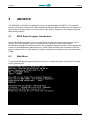
1
CPC306
PC/104-Plus
Vortex86DX Based
CPU Module
User Manual
Rev. 002a E
February 2012
Product Title:
Document name:
Manual version:
Ref. doc. v.:
CPC306
CPC306 User Manual
002a E
2.1 R (467444 031)
Copyright © 2011, 2012 Fastwel Co. Ltd. All rights reserved.
Revision Record
Rev. Index
Brief Description of Changes
Board Index
Date of Issue
001
Initial preliminary version (incomplete)
CPC306 PCB v.3.0 + KIB386
August 2011
002
Functional description and BIOS sections added
CPC306 PCB v.3.0 + KIB386
October 2011
002a
Dimensions corrected
CPC306 PCB v.3.0 + KIB386
February 2012
Contact Information
Fastwel Co. Ltd
Fastwel Corporation US
Address:
108 Profsoyuznaya st.,
Moscow 117437,
Russian Federation
45 Main Street, Suite 319
Brooklyn, New York 11201
USA
Tel.:
+7 (495) 232-1681
+1 (718) 554-3686
Fax:
+7 (495) 232-1654
+1 (718) 797-0600
Toll free:
E-mail:
[email protected]
Web:
http://www.fastwel.com/
+1 (877) 787-8443 (1-877-RURUGGED)
CPC306
Table of Contents
Table of Contents ..............................................................................................................................................1
List of Tables .....................................................................................................................................................3
List of Figures ....................................................................................................................................................3
Notation Conventions.........................................................................................................................................5
General Safety Precautions................................................................................................................................6
Unpacking, Inspection and Handling...................................................................................................................7
Three Year Warranty..........................................................................................................................................8
1
Introduction...................................................................................................................................... 9
1.1
1.2
1.3
1.4
2
Technical Specifications.................................................................................................................13
2.1
2.2
2.3
2.4
2.5
2.6
3
Module Introduction.................................................................................................................................9
CPC306 Versions..................................................................................................................................11
Delivery Checklist..................................................................................................................................11
Additional Accessories ..........................................................................................................................12
General.................................................................................................................................................13
Power Requirements.............................................................................................................................15
Environmental.......................................................................................................................................16
Mechanical ...........................................................................................................................................16
Dimensions and Weight.........................................................................................................................17
MTBF ...................................................................................................................................................18
Functional Description ...................................................................................................................19
3.1
3.2
CP C3 0 6
Structure and Layout .............................................................................................................................19
Functional Description...........................................................................................................................24
3.2.1
Vortex86DX SoC ..................................................................................................................24
3.2.2
SDRAM Memory...................................................................................................................25
3.2.3
IDE Interface.........................................................................................................................25
3.2.4
CompactFlash ......................................................................................................................26
3.2.5
ATA Flash Disk .....................................................................................................................27
3.2.6
PS/2 Keyboard and Mouse Interface......................................................................................27
3.2.7
Optoisolated Reset/IRQ Input................................................................................................28
3.2.8
USB Interface .......................................................................................................................29
3.2.9
Fast Ethernet Interface..........................................................................................................29
3.2.10
Serial Ports...........................................................................................................................30
3.2.10.1 COM1 and COM2 .................................................................................................30
3.2.10.2 COM3 and COM4 .................................................................................................33
3.2.11
Parallel Printer Port (LPT) .....................................................................................................34
3.2.12
Expansion Buses: ISA and PCI .............................................................................................35
3.2.12.1 PCI Header...........................................................................................................35
3.2.12.2 ISA Header...........................................................................................................37
3.2.13
Redundancy .........................................................................................................................39
3.2.14
Analog Input/Output ..............................................................................................................40
3.2.15
Discrete Input/Output (UNIO).................................................................................................40
3.2.16
Watchdog Timers..................................................................................................................41
3.2.17
RTC, CMOS, Serial FRAM and Reserved BIOS.....................................................................41
3.2.17.1 Reserved BIOS.....................................................................................................41
3.2.17.2 RTC, CMOS and Battery.......................................................................................41
Us e r
M a n u a l
1
© 2 0 1 2
F a s t w e l
v . 0 0 2 a
E
CPC306
3.3
4
External Connections .....................................................................................................................49
4.1
4.2
4.3
4.4
5
3.2.17.3 FRAM...................................................................................................................42
3.2.17.4 BIOS Upgrade ......................................................................................................42
3.2.18
Power Supply .......................................................................................................................42
3.2.19
Power Supply Supervisor ......................................................................................................43
3.2.20
GPIO Ports ...........................................................................................................................43
3.2.21
Configuration Jumpers ..........................................................................................................43
3.2.22
Diagnostic LEDs ...................................................................................................................44
3.2.23
Reset Button.........................................................................................................................44
Address Mapping ..................................................................................................................................45
3.3.1
Memory Addressing ..............................................................................................................45
3.3.2
I/O Addressing......................................................................................................................45
3.3.3
Interrupt Settings ..................................................................................................................47
3.3.4
DMA Channels......................................................................................................................48
Safety Regulations ................................................................................................................................49
Connection of Peripheral Devices ..........................................................................................................50
KIB386 Interface Adapter Module ..........................................................................................................51
Software Installation..............................................................................................................................54
AMI BIOS .........................................................................................................................................55
5.1
5.2
5.3
5.4
5.5
5.6
5.7
5.8
CP C3 0 6
BIOS Setup Program. Introduction.........................................................................................................55
Main Menu............................................................................................................................................55
Advanced .............................................................................................................................................57
5.3.1
CPU Configuration................................................................................................................58
5.3.2
IDE Configuration..................................................................................................................59
5.3.2.1
Primary IDE Master...............................................................................................60
5.3.3
Remote Access Configuration ...............................................................................................61
5.3.4
USB Configuration ................................................................................................................62
Advanced PCI/PnP Settings ..................................................................................................................63
Boot Options.........................................................................................................................................64
5.5.1
Boot Settings Configuration ...................................................................................................65
5.5.2
Boot Device Priority...............................................................................................................66
Security Settings ...................................................................................................................................67
Chipset Menu........................................................................................................................................68
5.7.1
NorthBridge Configuration.....................................................................................................69
5.7.2
SouthBridge Configuration ....................................................................................................70
5.7.2.1
ISA Configuration..................................................................................................71
5.7.2.2
Serial/Parallel Port Configuration...........................................................................72
5.7.2.3
WatchDog Configuration .......................................................................................73
Exit Menu .............................................................................................................................................74
Us e r
M a n u a l
2
© 2 0 1 2
F a s t w e l
v . 0 0 2 a
E
CPC306
List of Tables
Table 1.1:
Table 1.2:
Table 1.3:
Table 2.1:
Table 3.1:
Table 3.2:
Table 3.3:
Table 3.4:
Table 3.5:
Table 3.6:
Table 3.7:
Table 3.8:
Table 3.9:
Table 3.10:
Table 3.11:
Table 3.12:
Table 3.13:
Table 3.14:
Table 3.15:
Table 3.16:
Table 3.17:
Table 3.18:
Table 3.19:
Table 3.20:
Table 3.21:
Table 3.22:
Table 3.23:
Table 4.1:
Table 5.1:
Table 5.2:
Table 5.3:
Table 5.4:
Table 5.5:
Table 5.6:
Table 5.7:
Table 5.8:
Table 5.9:
Table 5.10:
Table 5.11:
Table 5.12:
Table 5.13:
Table 5.14:
Table 5.15:
Table 5.16:
Table 5.17:
Table 5.18:
CPC306 Versions.......................................................................................................................11
CPC306 Supplied Set.................................................................................................................11
CPC306 Additional Accessories..................................................................................................12
Power Supply Requirements.......................................................................................................15
IDE Channel: Devices Connection Variants.................................................................................25
XP17 Connector Pinout (IDE) .....................................................................................................25
XP34 CompactFlash Socket Pinout.............................................................................................26
XP27 Contacts Designation ........................................................................................................27
XP19 Connector Pinout (USB) ....................................................................................................29
XP15 Ethernet Header Pinout .....................................................................................................30
XP8 (COM1) and XP4 (COM2) Pin Assignments .........................................................................30
XP3 and XP7 Pinpads Jumpers ..................................................................................................31
XP13 and XP14 Pin Assignments ...............................................................................................33
XP11 (LPT) Connector Pinout.....................................................................................................34
XS1 Connector Contacts Designation (Rows A, B) ......................................................................35
XS1 Connector Contacts Designation (Rows C, D)......................................................................36
ISA XS2 Connector (Rows A and B) Contacts Designation ..........................................................37
ISA XS2 (Rows C and D) Contacts Designation ..........................................................................38
XP1 Pinout.................................................................................................................................40
XP2 Pinout.................................................................................................................................40
XP26 Power Connector Pinout....................................................................................................42
CPC306 Diagnostic LEDs Function.............................................................................................44
XP9 Contacts Function ...............................................................................................................44
Memory Address Mapping ..........................................................................................................45
I/O Address Space .....................................................................................................................45
Interrupt Settings........................................................................................................................47
DMA Settings .............................................................................................................................48
KIB386-01 and CPC306 Connectors Correspondence.................................................................54
Main Menu Items........................................................................................................................56
Advanced Menu Items ................................................................................................................57
CPU Configuration Items ............................................................................................................58
IDE Configuration Items..............................................................................................................59
Primary IDE Master Items...........................................................................................................60
Remote Access Configuration Items............................................................................................61
USB Configuration Items ............................................................................................................62
PCI / Plug and Play Menu Items..................................................................................................63
Boot Menu Items ........................................................................................................................64
Boot Settings Configuration Items ...............................................................................................65
Security Menu Items...................................................................................................................67
Chipset Menu Items....................................................................................................................68
NorthBridge Configuration Items .................................................................................................69
SouthBridge Configuration Items.................................................................................................70
ISA Configuration Items..............................................................................................................71
Serial/Parallel Ports Settings.......................................................................................................72
WDT0 and WDT1 Settings..........................................................................................................73
Exit Menu Items .........................................................................................................................74
List of Figures
Figure 1.1:
Figure 2.1:
Figure 3.1:
Figure 3.2:
Figure 3.3:
Figure 3.4:
CP C3 0 6
Us e r
CPC306 Module Appearance......................................................................................................10
CPC306: Overall and Mounting Dimensions................................................................................17
CPC306 Block Diagram..............................................................................................................19
Top Side: Connectors and Main Components Layout...................................................................22
Bottom Side: Connectors and Main Components Layout..............................................................23
Vortex86DX SoC Block Diagram.................................................................................................24
M a n u a l
3
© 2 0 1 2
F a s t w e l
v . 0 0 2 a
E
CPC306
Figure 3.5:
Figure 3.6:
Figure 3.7:
Figure 3.8:
Figure 3.9:
Figure 3.10:
Figure 3.11:
Figure 3.12:
Figure 3.13:
Figure 3.14:
Figure 3.15:
Figure 3.16:
Figure 3.17:
Figure 3.18:
Figure 3.19:
Figure 3.20:
Figure 3.21:
Figure 3.22:
Figure 3.23:
Figure 3.24:
Figure 3.25:
Figure 4.1:
Figure 4.2:
Figure 4.3:
Figure 4.4:
Figure 4.5:
Figure 5.1:
Figure 5.2:
Figure 5.3:
Figure 5.4:
Figure 5.5:
Figure 5.6:
Figure 5.7:
Figure 5.8:
Figure 5.9:
Figure 5.10:
Figure 5.11:
Figure 5.12:
Figure 5.13:
Figure 5.14:
Figure 5.15:
Figure 5.16:
Figure 5.17:
Figure 5.18:
Figure 5.19:
XP17 IDC44 Pins Numbering......................................................................................................25
XP27 Connector Contacts Numbering.........................................................................................27
XP25 Connector.........................................................................................................................28
Discrete Input Optoisolation and Reset or IRQ Source Selection..................................................28
XP19 Connector.........................................................................................................................29
XP15 Connector.........................................................................................................................30
XP8 and XP4 Pins Numbering ....................................................................................................30
XP3 and XP7 Pinpads ................................................................................................................31
RS485/422 Transmitter with Bias Elements and Terminating Resistors ........................................31
Connection of Several Devices in RS422 Mode...........................................................................32
Connection of Several Devices in RS485 Mode...........................................................................32
IDC10 Pins Numbering ...............................................................................................................33
XP20 Connector.........................................................................................................................34
XS1 Connector Contacts Layout .................................................................................................35
ISA Header Contacts Layout.......................................................................................................37
Redundancy Pinpads Connection ...............................................................................................39
XP1 Pinpad................................................................................................................................39
XP2 Pinpad................................................................................................................................40
XP26 Power Supply Connector...................................................................................................42
Power Supply Supervisor Diagram..............................................................................................43
External LEDs Connection (XP9) ................................................................................................44
External Devices Connection ......................................................................................................50
KIB386-01 Connections..............................................................................................................51
KIB386-01 Dimensions ...............................................................................................................52
KIB386-01 Layout, Top...............................................................................................................53
KIB386-01 Layout, Bottom..........................................................................................................53
Main Menu Screen Image...........................................................................................................56
Advanced Screen Image.............................................................................................................57
CPU Configuration Screen Image ...............................................................................................58
IDE Configuration Screen Image.................................................................................................59
Primary IDE Master Screen Image..............................................................................................60
Remote Access Configuration Screen Image...............................................................................61
USB Configuration Screen Image................................................................................................62
PCI / Plug and Play Menu Screen ...............................................................................................63
Boot Menu Screen......................................................................................................................64
Boot Settings Configuration Screen Image ..................................................................................65
Boot Device Priority Screen Image..............................................................................................66
Security Menu Screen ................................................................................................................67
Chipset Menu Screen Image.......................................................................................................68
NorthBridge Configuration Screen Image ....................................................................................69
SouthBridge Configuration Screen Image....................................................................................70
ISA Configuration Screen Image.................................................................................................71
Serial/Parallel Port Configuration Screen Image ..........................................................................72
WatchDog Configuration Screen Image.......................................................................................73
Exit Menu Screen Image.............................................................................................................74
All information in this document is provided for reference only, with no warranty of its suitability for any specific purpose. This information has been thoroughly checked and
is believed to be entirely reliable and consistent with the product that it describes. However, Fastwel accepts no responsibility for inaccuracies, omissions or their
consequences, as well as liability arising from the use or application of any product or example described in this document.
Fastwel Co. Ltd. reserves the right to change, modify, and improve this document or the products described in it, at Fastwel's discretion without further notice. Software
described in this document is provided on an “as is” basis without warranty. Fastwel assumes no liability for consequential or incidental damages originated by the use of
this software.
This document contains information, which is property of Fastwel Co. Ltd. It is not allowed to reproduce it or transmit by any means, to translate the document or to convert
it to any electronic form in full or in parts without antecedent written approval of Fastwel Co. Ltd. or one of its officially authorized agents.
Fastwel and Fastwel logo are trademarks owned by Fastwel Co. Ltd., Moscow, Russian Federation. Ethernet is a registered trademark of Xerox Corporation. IEEE is a
registered trademark of the Institute of Electrical and Electronics Engineers Inc. Intel is a trademark of Intel Corporation. Geode is trademark of AMD. Microsoft is a
trademark of the Microsoft corporation. In addition, this document may include names, company logos and trademarks, which are registered trademarks and, therefore,
are property of their respective owners.
Fastwel welcomes suggestions, remarks and proposals regarding the form and the content of this Manual.
CP C3 0 6
Us e r
M a n u a l
4
© 2 0 1 2
F a s t w e l
v . 0 0 2 a
E
CPC306
Notation Conventions
Warning, ESD Sensitive Device!
This symbol draws your attention to the information related to electro static sensitivity of your
product and its components. To keep product safety and operability it is necessary to handle
it with care and follow the ESD safety directions.
Warning!
This sign marks warnings about hot surfaces. The surface of the heatsink and some
components can get very hot during operation. Take due care when handling, avoid
touching hot surfaces!
Caution: Electric Shock!
This symbol warns about danger of electrical shock (> 60 V) when touching products or
parts of them. Failure to observe the indicated precautions and directions may expose your
life to danger and may lead to damage to your product.
Warning!
Information marked by this symbol is essential for human and equipment safety.
Read this information attentively, be watchful.
Note...
This symbol and title marks important information to be read attentively for your own benefit.
CP C3 0 6
Us e r
M a n u a l
5
© 2 0 1 2
F a s t w e l
v . 0 0 2 a
E
CPC306
General Safety Precautions
This product was developed for fault-free operation. Its design provides conformance to all related
safety requirements. However, the life of this product can be seriously shortened by improper
handling and incorrect operation. That is why it is necessary to follow general safety and
operational instructions below.
Warning!
All operations on this device must be carried out by sufficiently
skilled personnel only.
Warning!
When handling this product, special care must be taken not to hit
the heatsink (if installed) against another rigid object. Also, be
careful not to drop the product, since this may cause damage
to the heatsink, CPU or other sensitive components as well.
Please, keep in mind that any physical damage to this product
is not covered under warranty.
Note:
This product is guaranteed to operate within the published
temperature ranges and relevant conditions. However, prolonged
operation near the maximum temperature is not recommended by
Fastwel or by electronic chip manufacturers due to thermal stress
related failure mechanisms. These mechanisms are common to all
silicon devices, they can reduce the MTBF of the product by
increasing the failure probability. Prolonged operation at the lower
limits of the temperature ranges has no limitations.
Caution, Electric Shock!
Before installing this product into a system and before installing
other devices on it, always ensure that your mains power is switched
off.
Always disconnect external power supply cables during all handling
and maintenance operations with this module to avoid serious
danger of electrical shock.
CP C3 0 6
Us e r
M a n u a l
6
© 2 0 1 2
F a s t w e l
v . 0 0 2 a
E
CPC306
Unpacking, Inspection and Handling
Please read the manual carefully before unpacking the module or mounting the device into your
system. Keep in mind the following:
ESD Sensitive Device!
Electronic modules and their components are sensitive to static
electricity. Even a non-perceptible by human being static discharge
can be sufficient to destroy or degrade a component's operation!
Therefore, all handling operations and inspections of this product
must be performed with due care, in order to keep product integrity
and operability:
n
Preferably, unpack or pack this product only at EOS/ESD safe workplaces. Otherwise, it is
important to be electrically discharged before touching the product. This can be done by
touching a metal part of your system case with your hand or tool. It is particularly important
to observe anti-static precautions when setting jumpers or replacing components.
If the product contains batteries for RTC or memory back-up, ensure that the module is not
placed on conductive surfaces, including anti-static mats or sponges. This can cause shortcircuit and result in damage to the battery and other components.
Store this product in its protective packaging while it is not used for operational purposes.
n
n
Unpacking
The product is carefully packed in an antistatic bag and in a carton box to protect it against
possible damage and harmful influence during shipping. Unpack the product indoors only at a
temperature not less than +15°C and relative humidity not more than 70%. Please note, that if the
product was exposed to the temperatures below 0°С for a long time, it is necessary to keep it at
normal conditions for at least 24 hours before unpacking. Do not keep the product close to a heat
source.
Following ESD precautions, carefully take the product out of the shipping carton box. Proper
handling of the product is critical to ensure correct operation and long-term reliability. When
unpacking the product, and whenever handling it thereafter, be sure to hold the module preferably
by the front panel, card edges or ejector handles. Avoid touching the components and connectors.
Retain all original packaging at least until the warranty period is over. You may need it for
shipments or for storage of the product.
Initial Inspection
Although the product is carefully packaged, it is still possible that shipping damages may occur.
Careful inspection of the shipping carton can reveal evidence of damage or rough handling. Should
you notice that the package is damaged, please notify the shipping service and the manufacturer
as soon as possible. Retain the damaged packing material for inspection.
After unpacking the product, you should inspect it for visible damage that could have occurred
during shipping or unpacking. If damage is observed (usually in the form of bent component leads
or loose socketed components), contact Fastwel's official distributor from which you have
purchased the product for additional instructions. Depending on the severity of the damage, the
product may even need to be returned to the factory for repair. DO NOT apply power to the product
if it has visible damage. Doing so may cause further, possibly irreparable damage, as well as result
in a fire or electric shock hazard.
If the product contains socketed components, they should be inspected to make sure they are
seated fully in their sockets.
CP C3 0 6
Us e r
M a n u a l
7
© 2 0 1 2
F a s t w e l
v . 0 0 2 a
E
CPC306
Handling
In performing all necessary installation and application operations, please follow only the
instructions supplied by the present manual.
In order to keep Fastwel’s warranty, you must not change or modify this product in any way, other
than specifically approved by Fastwel or described in this manual.
Technical characteristics of the systems in which this product is installed, such as operating
temperature ranges and power supply parameters, should conform to the requirements stated by
this document.
Retain all the original packaging, you will need it to pack the product for shipping in warranty cases
or for safe storage. Please, pack the product for transportation in the way it was packed by the
supplier.
When handling the product, please, remember that the module, its components and connectors
require delicate care. Always keep in mind the ESD sensitivity of the product.
Three Year Warranty
Fastwel Co. Ltd. (Fastwel), warrants that its standard hardware products will be free from defects
in materials and workmanship under normal use and service for the currently established warranty
period. Fastwel’s only responsibility under this warranty is, at its option, to replace or repair any
defective component part of such products free of charge.
Fastwel neither assumes nor authorizes any other liability in connection with the sale, installation
or use of its products. Fastwel shall have no liability for direct or consequential damages of any
kind arising out of sale, delay in delivery, installation, or use of its products.
If a product should fail through Fastwel's fault during the warranty period, it will be repaired free of
charge. For out of warranty repairs, the customer will be invoiced for repair charges at current
standard labor and materials rates.
Warranty period for Fastwel products is 36 months since the date of purchase.
The warranty set forth above does not extend to and shall not apply to:
1.
Products, including software, which have been repaired or altered by other than
Fastwel personnel, unless Buyer has properly altered or repaired the products in
accordance with procedures previously approved in writing by Fastwel.
2.
Products, which have been subject to power supply reversal, misuse, neglect,
accident, or improper installation.
Returning a product for repair
1.
Apply to Fastwel company or to any of the Fastwel's official representatives for the
Product Return Authorization.
2.
Attach a failure inspection report with a product to be returned in the form, accepted by
customer, with a description of the failure circumstances and symptoms.
3.
Carefully package the product in the antistatic bag, in which the product had been
supplied. Failure to package in antistatic material will VOID all warranties. Then
package the product in a safe container for shipping.
4.
The customer pays for shipping the product to Fastwel or to an official Fastwel
representative or dealer.
CP C3 0 6
Us e r
M a n u a l
8
© 2 0 1 2
F a s t w e l
v . 0 0 2 a
E
Introduction
1
CPC306
Introduction
This document presents general information on CPC306 CPU module, the details of its proper and
safe installation, configuration and operation. The issues of PC/104 modules and external devices
connection are also considered. This document applies to the module with PCB version 3.0;
version is indicated on board.
1.1
Module Introduction
Fastwel CPC306 is designed for applications requiring high-performance low-power industrial
controller being able to process a wide range of analog and discrete signals. Fastwel CPC306
conforms to PC/104-Plus specification and is compatible with a large number of PC/104 and
PC/104-Plus peripheral and power supply modules delivered by a wide range of manufacturers.
Based on x86-compatible Vortex86DX System-on-Chip (SoC) operating at 600 MHz, the module
bears 256 MB soldered DDR2 memory and wide range of input/output interfaces. CPC306 allows
system designers simple programming and provides portability of previously developed libraries for
x86 architecture with MS DOS 6.22, FreeDOS, Windows CE 5.0, Linux 2.6, and QNX 6.4 support.
Integrated Ethernet channel, four COM ports and large number of digital and analog input/output
ports give developers an excellent set of interconnects to the sensors, slave devices and host
systems. Four USB 2.0 and LPT ports give CPC306 connectivity to various devices from PC
environment.
Full 16-bit ISA bus support ensures expansion capability of CPC306 with legacy peripheral
modules and power supplies, while 32-bit PCI provides interconnect for mainstream expansion
modules.
CPC306 has onboard CF and EIDE interfaces, providing developers a choice of storage media to
be used with. With all components soldered on board CPC306 withstands vibration up to 10g,
shock up to 100g.
For debugging purposes or for applications requiring graphical interface, CPC306 can operate
together with Fastwel VIM301 graphics controller module providing VGA, LVDS, TFT, and SGD
interfaces. KIB386 interface adapter module can be used for connection of external devices via
standard interface connectors.
The module is designed for operation at temperatures from -40°C to +85°C.
CP C3 0 6
Us e r
M a n u a l
9
© 2 0 1 2
F a s t w e l
v . 0 0 2 a
E
Introduction
CPC306
Figure 1.1:
CPC306 Module Appearance
The appearance may vary for different versions of the module.
CP C3 0 6
Us e r
M a n u a l
10
© 2 0 1 2
F a s t w e l
v . 0 0 2 a
E
Introduction
CPC306
1.2
CPC306 Versions
At the present time the CPC306 module is manufactured in two versions differing in interface
capabilities.
Table 1.1:
CPC306 Versions
Name
CPC306
controller module
Version
Features
CPC306-01
Analog and discrete input/output
CPC306-02
No analog and discrete input/output
Other options include:
\COATED – protective coating;
1.3
\CE
– Windows CE 5 preinstalled;
\LNX
– Linux 2.6 preinstalled;
\QNX
– QNX 6.4.1 preinstalled
Delivery Checklist
Table 1.2:
CPC306 Supplied Set
Name
Description
CPC30601
CPC30602
CPC306 processor module
ACS00023
DSUB9M to IDC10 2 mm adapter cable for connection to COM port (685611.082)
–
Mounting standoffs kit
–
Jumpers set
–
Antistatic bag and consumer carton box
Note:
Keep the antistatic bag and the original package at least until the warranty period
is over. It can be used for future storage or warranty shipments.
CP C3 0 6
Us e r
M a n u a l
11
© 2 0 1 2
F a s t w e l
v . 0 0 2 a
E
Introduction
CPC306
1.4
Additional Accessories
Peripheral devices are attached to the module directly or via additional accessories and cables
listed in the following table. Additional accessories are not supplied with the CPU module, are
ordered separately.
Table 1.3:
CPC306 Additional Accessories
Name
Description
KIB386-01
Interface module with installed standard PC interface connectors
CDM02
Adapter module for connection of 3.5" HDD or CD-ROM drive (469535.023)
ACS00010
FC44 cable for 2.5" HDD connection to 44-contact header
ACS00031-01
PHR-5 connector set. Includes JST PHR-5 socket and a set of contacts
SPH-002T-P0.5S for connection to XP4 or XP8 headers of the module
ACS00031-02
PHR-5 connector set. Includes JST PHR-2 socket and a set of contacts
SPH-002T-P0.5S for connection to XP27 header of the module
ACS00038
Connector set for connection of a power supply unit to the module.
Includes AMP 4-171822-4 socket and a set of contacts 170262-1 for connection
to XP26 power connector of the module
ACS00040-01,
ACS00040-03,
ACS00040-04,
ACS00040-05
IDC2 socket for ribbon cable
with 10, 26, 20, 44 contacts respectively.
Recommended counterpart for IDC2 headers of the module
ACS00042
Null modem cable
ACS00043
PS/2 cable. Cable length: 200 mm. Connectors: PS/2 and JST PHR-6 socket.
Recommended counterpart for XP27 header of the module
ACS00047,
ACS00047-03,
ACS00047-05
2 mm pitch one row сontact holder (socket) for 2, 6, 14 contacts respectively.
Recommended counterpart for XP1, XP9, XP25, XP33 headers of the module
ACS00048,
ACS00048-02,
ACS00048-03,
ACS00048-04
2 mm pitch two row сontact holder (socket) for 10, 26, 20, 44 contacts
respectively. Recommended counterpart for IDC headers of the module
Set of contacts for contact holders (sockets) ACS00047 and ACS00048:
- Set of contacts, 10 pcs.
- One contact crimped on MGTF 1x0.14 wire, 1 m length
- Contact crimped on MGTF 1x0.14 wire, 1 m length, 5 pcs.
ACS00049
ACS00049-01,
ACS00049-02
CP C3 0 6
Us e r
M a n u a l
12
© 2 0 1 2
F a s t w e l
v . 0 0 2 a
E
Technical Specifications
CPC306
2
Technical Specifications
2.1
General
n
n
n
n
n
n
n
n
n
CP C3 0 6
Form-factor:
§
PC/104-Plus
CPU: Integrated in DM&P Vortex86DX SoC
§
600 MHz
§
32-bit x86 compatible core
§
16-bit memory bus
§
Math coprocessor
§
32 KB L1, 256 KB L2 cache
§
6-stage pipeline
System memory:
§
256 MB soldered DDR2 SDRAM
§
DDR333
IDE port:
§
One IDE channel (Primary)
§
Support for up to two UltraDMA-100 IDE devices with NAND Flash disabled
in BIOS Setup and if the CompactFlash socket (XP34) is not populated
CompactFlash socket
§
Type I/II
§
Bottom side location
Solid State Disk
§
Soldered
§
1 GB NAND flash
§
IDE interface
§
Can be used as bootable device
§
UltraDMA/100 support
PS/2:
§
PS/2 keyboard and mouse interface
Remote Reset/IRQ:
§
Discrete remote reset/interrupt input
§
500V optoisolation
USB:
§
Four USB 2.0 channels
§
One device can be connected to each channel
Us e r
M a n u a l
13
© 2 0 1 2
F a s t w e l
v . 0 0 2 a
E
Technical Specifications
n
n
n
n
n
n
CPC306
LAN:
§
Two Fast Ethernet ports 10/100 Mbit/s
§
500 V isolation
Serial ports:
§
Four serial ports
§
High speed NS16C550 compatible
§
COM1, COM2: RS422/485, up to 115.2 Kbaud, 500 V isolation
§
COM3, COM4: RS232, complete, up to 115.2 Kbaud
§
Console operation via COM1 ... COM4
Parallel port:
§
SPP/ECP/EPP compatible
Expansion buses:
§
PCI and ISA
Redundancy support
Analog input port:
§
8 input channels
§
ADC resolution: 12 bit
§
Voltage measurement ranges: 0...+5V; ±5V; 0...+10V; ±10V;
Max basic reduced error: 0.3%
Current measurement ranges: 0...20 mA; ±20 mA;
Max basic reduced error: 0.3%
§
Hardware averaging: N=1, 4, 8 or 16 samples
§
Conversion time for one ADC channel: 12.5 ms*N
§
Input resistance: 200 kohm
§
External shunt resistance (current measurement): 249 ohm
§
Overvoltage protection: ±16.5 V
§
Isolation voltage: min 500 V
Analog output port:
§
2 output channels
§
DAC resolution: 12 bit
§
n
§
n
n
CP C3 0 6
Output ranges: 0...+5V; ±5V; 0...+10V
Max basic reduced error: ±0.6%
§
Max conversion time for one DAC channel: 10 ms
§
Min output resistance: 2 kohm
§
Isolation voltage: min 500 V
Universal discrete I/O port:
§
72 CMOS/TTL lines;
§
Output capacity of logic 0 / logic 1, max: 12.0 / 4.0 mA
§
Output capacity for opto-modules: 20 mA
§
In-system programming
§
The lines [71:48] can be programmed as LCD and matrix keyboard ports
Three watchdog timers:
§
One with fixed timeout period of 1.6 s
§
Two integrated in Vortex86DX with programmable timeout period
Us e r
M a n u a l
14
© 2 0 1 2
F a s t w e l
v . 0 0 2 a
E
Technical Specifications
n
CPC306
Flash BIOS:
§
Main BIOS: 512 KB, soldered, ISA bus
§
Reserve BIOS: 256 KB, integrated in the controller
§
In-system modification
§
Automatic switching
RTC:
§
On-board real time clock with Li battery backup
Safety:
§
System configuration settings stored in CMOS+Serial FRAM (256 Kb)
§
Possibility of batteryless operation
Software support:
§
AMI BIOS
§
Software compatibility with FreeDOS, MS DOS 6.22, Windows CE 5, QNX 6.4,
and Linux 2.6 operating systems
n
n
n
2.2
Power Requirements
The module can be powered via XS1 and XS2 connectors. Additionally, power can be supplied via
XP26 (4-contact AMP 4-171826-4) power connector by an external DC power source; polarity
reversal and overvoltage protection provided.
Power supply unit should provide starting current, which is 5.6 A for 0.5 ms for CPC306-01 version
and 4.2 A for 0.5 ms for CPC306-02. It is allowed to use power supply units with current limiting not
less than 1.5 A. Selecting a power supply unit, the starting current should be considered as well as
the consumption current of expansion modules.
Consumption current typical valuation is 0.6 A.
Table 2.1:
Power Supply Requirements
Connectors
Power Voltage
Voltage Limits
Consumption
current
Starting
current
PC/104 and PCI-104
+5 V
+4.75V to +5.25V
1.3 A
5.6 A
XP26 (auxiliary power
connector)
+5 V
+4.75V to +5.25V
1.3 A
5.6 A
Polarity reversal and
overvoltage protection ±26V
Important:
Please, find important notes on power supply in subsection 3.2.17
of this document.
CP C3 0 6
Us e r
M a n u a l
15
© 2 0 1 2
F a s t w e l
v . 0 0 2 a
E
Technical Specifications
2.3
CPC306
Environmental
n
Operating temperature range: –40°C to +85°C
n
n
Storage temperature: –55°C to +90°C
Relative humidity: 5% to 90% at 25°С, noncondensing
Note:
Protective coating of CPC306 versions makes them resistant to
damp heat cyclic exposure at temperatures up to +55±2°C and
relative humidity of up to 93±3%.
2.4
Mechanical
n
n
n
n
Vibration (5 ... 50 Hz) – 1 mm amplitude;
Vibration (50 ... 2000 Hz) – 10g;
Single shock, peak acceleration – 150 g;
Multiple shock, peak acceleration – 50 g.
Important:
If CPC306 is operated in rugged environment, it is recommended
to additionally fasten counterparts on connectors.
CP C3 0 6
Us e r
M a n u a l
16
© 2 0 1 2
F a s t w e l
v . 0 0 2 a
E
Technical Specifications
2.5
CPC306
Dimensions and Weight
n
Weight:
n
Version
Weight, kg
CPC306-01
0.150
CPC306-02
0.135
Dimensions, max:
103.5 × 115.8 × 23.7 mm (4.07” × 4.56” × 0.93”)
(dimensions may differ within PCB manufacturing tolerance, ±0.8 mm)
Figure 2.1:
CPC306: Overall and Mounting Dimensions
21.6
73.7
1
1
1
3.2
11.1
1.6
1
D1
C1
B1
A1
1
1
1
1
1
1
1
1
1
79.3
85.7
96.6
1
1
1
1
1
1
HCS0905H
1
1
1
1
B1
A1
1
1
1
C0
D0
1
1
1
1
1
1
6.9 max
80
11
90.2
115.8
The module is built according to PC/104-Plus specification v.2.0. On the bottom side there are
deviations in maximum (4.83 mm) components hight: CompactFlash socket (XP34, 8.3 mm) and
Ethernet port transformers (T1 and T2, 5.97 mm). On the top side there is insignificant deviation in
maximum (8.76 mm) component hight: DA6 microcircuit is 8.9 mm high.
CP C3 0 6
Us e r
M a n u a l
17
© 2 0 1 2
F a s t w e l
v . 0 0 2 a
E
Technical Specifications
2.6
CPC306
MTBF
n
MTBF for CPC306 is 170000 hours.
The value is calculated according to: Telcordia Issue 1 model, Method I Case 3, for continuous operation
at a surface location, at normal environmental conditions and at ambient temperature 30°С.
CP C3 0 6
Us e r
M a n u a l
18
© 2 0 1 2
F a s t w e l
v . 0 0 2 a
E
Functional Description
CPC306
3
Functional Description
3.1
Structure and Layout
Functional diagram of the CPC306 module is shown in Figure 3.1.
Figure 3.1:
CPC306 Block Diagram
PC/104-plus Connector (PCI)
Isolated 500V
DC/DC
RS-485
MAX1486
RS-485
MAX1486
Isolated 500V
ADuM
1301
ADuM
1301
DC/DC
(+3.3V)
CR2032
(Battery
Holder)
PCI
DC/DC
(+1.8V)
DC/DC
(+1.2V)
Isolated 500V
LU82551
HX1188
DC/DC
LAN
(1, 2)
HX1188
DDRII
SDRAM
Compact
Flash
Isolated 500V
Vortex86DX
SoC
256 MB
IDE
BIOS
EEPROM
256KB
IDE
(44 pin)
SST
55LD019A
(ATA Flash
Disk)
1 GB
NAND Flash
Spartan
XCS05
(FPGA)
Isolated 500V/channel
DC/DC
2
SPI
AD7249
ADuM
1301
Analog
I/O
8
RS232
ADM213E
RS232
ADM213E
FRAM
ADuM
1301
256 Kb
DC/DC
4x USB 2.0
USB
(1, 2, 3, 4)
Speaker
24
Discrete
I/O
24
Discrete
I/O
24
Discrete
I/O
LPT
LPT
Spartan
XCS20
(FPGA)
PS/2
PS/2
Redundancy
XP2
MAX1270
MAX
4866LEUT
+5V
ISA
BIOS
Ext
LEDs
header
JTAG
XP5
+5V In
Reset#
SW1
Optional
Power
CP C3 0 6
Us e r
M a n u a l
PC/104 Connector (ISA)
19
© 2 0 1 2
F a s t w e l
v . 0 0 2 a
E
Functional Description
CPC306
CPC306 includes the following main functional units:
n
n
n
n
n
n
n
n
n
n
n
n
n
n
n
n
CP C3 0 6
DM&P Vortex86DX SoC
256 MB soldered DDR2 SDRAM system memory;
IDE port with support for up to two UltraDMA/100 devices (primary channel only);
CompactFlash socket for Type I/II cards;
ATA flash disk controller; onboard NAND flash-disk, 1 GB;
PS/2 keyboard/mouse port;
Optoisolated (500V) remote Reset/interrupt input;
Four USB 1.1/2.0 channels;
Two Fast Ethernet controllers, 10/100 Mbit/s, 500V isolation;
Serial ports:
§
COM1, COM2: RS422/485, up to 115.2 Kbaud, 500V isolation;
§
COM3, СОМ4: RS232, up to 115.2 Kbaud, complete;
§
Console operation via COM1 ... COM4
Universal parallel port (LPT), SPP/ECP/EPP compatible
PCI and ISA expansion buses
Redundancy support
Analog input port:
§
8 channels
§
12-bit resolution
§
Voltage measurement ranges: 0..+5 V, 0..+10 V, ±5 V, ±10 V;
max permissible basic reduced error within operating temp range: 0.3%
§
Current measurement ranges: ±20 mA, 0..20 mA
max permissible basic reduced error within operating temp range: 0.3%
§
Hardware averaging for 1, 4, 8, or 16 samples
§
Min conversion time for one ADC channel: 12.5 ms * N
§
Input resistance of a channel in voltage measurement mode (RIN): 200 kohm
§
Shunt resistor for current measurement (RSHUNT): 249 ohm ± 0.05%
§
Overvoltage protection: ±16.5 V
§
500V isolation
Analog output port:
§
2 channels
§
12-bit resolution
§
Output ranges: 0..+5 V, ±5 V, 0..+10 V;
max permissible basic reduced error within operating temp range: 0.6%
§
Conversion time for one DAC channel: 10 ms max
§
Min output load: 2 kohm
§
500V isolation
Universal discrete I/O port:
§
72 CMOS/TTL lines
§
Output capacity Log. “0” / Log. “1”: 12.0 mA / 4.0 mA
§
Output capacity for opto modules (w/o keeping signal level): 20 mA max
§
In-system programming
§
[71:48] lines can be used as a matrix keyboard and LCD port
Us e r
M a n u a l
20
© 2 0 1 2
F a s t w e l
v . 0 0 2 a
E
Functional Description
n
n
n
n
CPC306
Three watchdog timers:
§
One with fixed timeout period of 1.6 s
§
Two integrated in Vortex86DX with programmable timeout period
Flash memory based reserved BIOS:
§
256 KB, integrated in controller (reserve);
§
512 KB on flash memory chip connected to ISA bus (main)
§
In-system modification
§
Auto loading from reserve copy, if loading from the main failed
Real time clock with Li battery backup;
CMOS memory and non-volatile FRAM (256 Kbit) for BIOS configuration storage;
Layouts of main CPC306 components and connectors on top and bottom sides are presented in
Figures 3.2 and 3.3 respectively.
External connections are illustrated in Chapter 4.
CP C3 0 6
Us e r
M a n u a l
21
© 2 0 1 2
F a s t w e l
v . 0 0 2 a
E
Functional Description
Figure 3.2:
CPC306
Top Side: Connectors and Main Components Layout
Reset
1
COM2
1
XP5
1
XP2
1
D1
C1
B1
A1
XP3 SW1
XP4
XP1
HL3
HL4 HL2
XP9
1
XP6
XP43
1
XS1
1
1
XP7
XP8
AIO
XP45
COM1
1
1
XP13 XP14
1
XP17
1
1
XP16
COM3 COM4
XP20
1
XP19
1
DIOA
X1
DIOB
USB
LPT
DIOC
HCS0905H
1
1
XP22
XS2
XP35
1
1
XP23
1
1
1
Optional Power
Connector
XP21
1
IDE
1
LAN 1,2
XP18
1
BIOS
1
XP15
1
D5
HL1 XP28
1
1
1
1
XP24
1
XP29 XP30 XP33 XP32 XP25
XP26 XP27
The layout may slightly differ for various versions of the module.
CP C3 0 6
Us e r
M a n u a l
22
© 2 0 1 2
F a s t w e l
v . 0 0 2 a
E
Functional Description
Figure 3.3:
CPC306
Bottom Side: Connectors and Main Components Layout
XS1
XP34
T1
T2
XS2
The layout may slightly differ for various versions of the board.
CP C3 0 6
Us e r
M a n u a l
23
© 2 0 1 2
F a s t w e l
v . 0 0 2 a
E
Functional Description
CPC306
3.2
Functional Description
3.2.1
Vortex86DX SoC
DM&P Vortex86DX includes the following main functional units:
32-bit х86 compatible core operating at 600 MHz;
32 KB L1, 256 KB L2 cache;
Math coprocessor;
16-bit DDR2 SDRAM memory bus;
IDE/SD controller;
Five RS-232 serial ports;
Universal parallel port;
Four USB 2.0 ports;
PS/2 keyboard/mouse port;
PCI, ISA, LPC, and SPI bus controllers;
Two I2C interfaces;
Built-in Ethernet 10/100 controller;
RTC;
CMOS memory for configuration storage;
Integrated flash-memory for BIOS storage;
Integrated redundancy system;
Two programmable watchdog timers.
n
n
n
n
n
n
n
n
n
n
n
n
n
n
n
n
n
Figure 3.4:
Vortex86DX SoC Block Diagram
LAN
USB 2.0
DDR2 SDRAM BUS
LPT
SoC
Vortex86DX CPU
North Bridge
South Bridge
DDR2 SDRAM Controller
LPC BUS
10/100Mbit LAN
GPIO
FPU
USB 2.0
REDUNDANCY + COM9
256 KB
L2 Cache
LPT
WATCHDOG
Primary IDE/
SD controller
COM 1,2 (RS-232/422 Mode)
Internal SPI BUS
COM 3,4 (RS-232 Mode)
LPC BUS
Vortex86 CPU
16KB
DATA
Cache
16KB
CODE
Cache
SPI Flash BIOS
256KB
2x I2C BUS
External SPI
BUS
GPIO
COM 9
(Rx/Tx)
COM 1,2
(RS-232/422
Mode)
COM 3,4
(RS-232 Mode)
RTC
Speaker
Vcore
Vio
Vmem
Battery
JTAG Debug Port
CP C3 0 6
Us e r
M a n u a l
IDE/SD BUS
I2C BUS
SPI BUS
24
PCI BUS
32.768KHz
© 2 0 1 2
F a s t w e l
v . 0 0 2 a
E
Functional Description
3.2.2
CPC306
SDRAM Memory
Two DDR2 SDRAM memory chips operating at 266 MHz are soldered on board. Total memory
size is 256 MB.
3.2.3
IDE Interface
One-channel IDE controller allows connection of up to two IDE devices. UDMA-100 mode is
supported.
If soldered NAND flash disk is enabled, one external device can be connected to XP17 or
CompactFlash card with no external devices. If the onboard flash disk is disabled, two external
drives can be connected as illustrated in the following table.
Table 3.1:
IDE Channel: Devices Connection Variants
Onboard Flash Disk
XP17 (Primary IDE)
XP34 (CompactFlash)
Enabled
No connection
No connection
Enabled
One device
No connection
Enabled
No connection
One device
Disabled
Two devices
No connection
Disabled
One device
One device
Figure 3.5:
XP17 IDC44 Pins Numbering
2
44
1
43
IDE interface is routed to XP17 connector. It is 2 mm pitch
2-row IDC44 pin header (Leotronics 4446-3440). Its pinout is
presented in the table below.
Recommended counterpart is Leotronics 2040-3442 socket
for ribbon cable (available as ACS00040-05 set) or
Leotronics 2067-2442 socket (ACS00048-04 set) and
2023-2000 contacts set (ACS00049).
Table 3.2:
XP17 Connector Pinout (IDE)
Pin#
Signal
Pin#
Signal
Pin#
Signal
Pin#
Signal
1
/RESET
12
DD12
23
/IOWR
34
/PDIAG
2
GND
13
DD2
24
GND
35
DA0
3
DD7
14
DD13
25
/IORD
36
DA2
4
DD8
15
DD1
26
GND
37
/CS0
5
DD6
16
DD14
27
/IOCHRDY
38
/CS1
6
DD9
17
DD0
28
GND
39
DASP
7
DD5
18
DD15
29
/DACK
40
GND
8
DD10
19
GND
30
GND
41
+5V
9
DD4
20
–
31
IRQ
42
+5V
10
DD11
21
DRQ
32
/CS16
43
GND
11
DD3
22
GND
33
DA1
44
–
CP C3 0 6
Us e r
M a n u a l
25
© 2 0 1 2
F a s t w e l
v . 0 0 2 a
E
Functional Description
CPC306
The ACS00010 (FC44) cable allows direct connection of a 2.5" HDD to the XP17 connector. Other
IDE devices (3.5" HDD, CD-ROM) having 40-contact 2.5 mm pitch connector can be connected to
CPC306 via the CDM02 (469535.023) adapter. This adapter is plugged directly to the 40-contact
connector of the IDE device, and with ACS00010 cable is connected to XP17 connector of
CPC306.
The operation modes of external IDE devices are set using jumpers on these devices.
3.2.4
CompactFlash
One CompactFlash Type I/II card can be connected to CPC306 using XP34 socket on the bottom
side (3M N7E50-M516RB-50). The socket is connected to Primary IDE channel. Booting from
CompactFlash is available. Master mode is enabled by closing contacts 2 and 3 at XP28
connector; Slave mode is enabled if these contacts are open (jumper removed).
Table 3.3:
XP34 CompactFlash Socket Pinout
Pin #
Function
Pin #
Function
1
GND
26
CD1#
2
D03
27
D11
3
D04
28
D12
4
D05
29
D13
5
D06
30
D14
6
D07
31
D15
7
CS0#
32
CS1#
8
A10 (not used)
33
VS1#
9
ATA SEL#
34
IORD#
10
A09 (not used)
35
IOWR#
11
A08 (not used)
36
WE#
12
A07 (not used)
37
INT
13
VCC (+3.3V)
38
VCC (+3.3V)
14
A06 (not used)
39
CSEL#
15
A05 (not used)
40
VS2#
16
A04 (not used)
41
RESET#
17
A03 (not used)
42
IORDY
18
A02
43
INPACK# (DRQ)
19
A01
44
REG# (DACK#)
20
A00
45
DASP#
21
D00
46
PDIAG#
22
D01
47
D08
23
D02
48
D09
24
IOCS16#
49
D10
25
CD2#
50
GND
CP C3 0 6
Us e r
M a n u a l
26
© 2 0 1 2
F a s t w e l
v . 0 0 2 a
E
Functional Description
3.2.5
CPC306
ATA Flash Disk
CPC306 has ATA flash disk controller connected to Primary IDE interface. The capacity of the
soldered on-board NAND flash memory chip is 1 GB. The system detects this controller as an IDE
disk which can be used as bootable.
Closing contacts 1-2 of XP28 sets Master mode for the controller; Slave mode is set by removing
jumper from these contacts.
The controller can be disabled by closing contacts 4-5 of XP28 (while jumper must be removed
from contacts 1-2 of XP28) or in BIOS Setup->Advanced.
3.2.6
PS/2 Keyboard and Mouse Interface
PS/2 keyboard and mouse interface is routed to XP27 6-pin 2 mm pitch IDC6 header
(JST B 6B-PH-KL).
Figure 3.6:
XP27 Connector Contacts Numbering
To make a custom cable it is recommended to use as a counterpart
connector JST PHR-6 socket with SPH-002T-P0.5S contact set
(available for order as ACS00031-02).
The following table shows pinout of CPC306 XP27 connector.
Table 3.4:
XP27 Contacts Designation
Pin #
Signal
Pin #
Signal
1
KBD CLK
4
GND
2
KBD DATA
5
+5V
3
MOUSE CLK
6
MOUSE DATA
CP C3 0 6
Us e r
M a n u a l
27
© 2 0 1 2
F a s t w e l
v . 0 0 2 a
E
Functional Description
3.2.7
CPC306
Optoisolated Reset/IRQ Input
Figure 3.7:
XP25 Connector
XP25 is a 2-pin 2 mm pitch IDC2 connector (PLS2-40/2) that is intended
for connection of a remote Reset/IRQ signal source with voltage of
3 to 5 V. The discrete input has 500 V optoisolation.
Recommended counterpart is Leotronics 2018-3021 socket (ordering code ACS00047) and 20232000 contact set (ACS00049).
Figure 3.8:
Discrete Input Optoisolation and Reset or IRQ Source Selection
+3.3V
+3V - +5V
XP25
1
2
External
Reset
R172
10K
R177
XP29
1
Reset#
2
DA16
3
470
XP35
IOCHK#
GPIO1[0]
4
GND
PFO#
(Supervisory Circuit)
Depending on position of jumpers of XP29 pin header, the input is connected to different circuits:
n
Closing contacts 1-2 of XP29 enables Reset on input;
n
Closing contacts 2-3 of XP29 connects input to line 0 of GPIO1 port. Selection Reset
function or IRQ line number is possible in BIOS Setup utility or by programming
registers of GPIO1 port.
n
Closing contacts 2-3 of XP29 and 1-2 of XP35 enables NMI interrupt generation on
input. This position of jumpers connects the input to IOCHK# line of ISA bus.
XP29 pinpad also allows to set function of PFO# signal (Power Fail Output) from Power voltage
supervisor chip. See also “Configuration Jumpers”, “Power Supply Supervisor”, and “GPIO Ports”
sections of this document.
CP C3 0 6
Us e r
M a n u a l
28
© 2 0 1 2
F a s t w e l
v . 0 0 2 a
E
Functional Description
3.2.8
CPC306
USB Interface
The module is equipped with four USB 2.0 host ports routed to XP19 header. USB 1.1 and
USB 2.0 modes are supported. Operation mode is selected in BIOS Setup -> Advanced. Each
channel has separate power control and protection circuit (+5V, 500 mA). One USB device may be
connected to each port. USB drive boot is supported.
XP19 is a 2-row IDC20 pin header (Leotronics 2073-3202) with 2 mm pitch.
Figure 3.9:
XP19 Connector
USB devices can be connected to XP19 header using a custom adaptor cable with Leotronics
2040-3202 socket for ribbon cable (order code ACS00040-04) or Leotronics 2022-2202 socket
(ACS00048-03) with 2023-2000 contacts (ACS00049).
Table 3.5:
XP19 Connector Pinout (USB)
Pin Number
Signal
Pin Number
Signal
1
+5V (USB1)
2
+5V (USB4)
3
D1-
4
D4-
5
D1+
6
D4+
7
GND (USB1)
8
GND (USB4)
9
–
10
–
11
+5V (USB2)
12
+5V (USB3)
13
D2-
14
D3-
15
D2+
16
D3+
17
GND (USB2)
18
GND (USB3)
19
–
20
–
3.2.9
Fast Ethernet Interface
There are two Fast Ethernet channels available onboard CPC306. One Ethernet controller is
integrated in Vortex86DX SoC; another Ethernet controller – Intel LU82551IT – is connected to PCI
bus. Both ports are not intended for use with network cables passing outside the building.
is available via XP8 connector on all versions of CPC306 except CPC30601. Ethernet controller is
integrated in Vortex86DX SoC.
CP C3 0 6
Us e r
M a n u a l
29
© 2 0 1 2
F a s t w e l
v . 0 0 2 a
E
Functional Description
Figure 3.10:
CPC306
XP15 Connector
2
10
1
9
Both Ethernet ports are routed to XP15
(2-row 2 mm pitch IDC10 header Leotronics 2073-3102).
Recommended counterpart – 2040-3102 socket for ribbon cable (ordering
code ACS00040-01) or Leotronics 2022-2102 socket (ACS00048) with
2023-2000 contacts (ACS00049).
Table 3.6:
XP15 Ethernet Header Pinout
Pin #
Signal
Pin #
Signal
1
LAN1_TX+
6
NC
2
LAN1_TX-
7
LAN2_TX+
3
LAN1_RX+
8
LAN2_TX-
4
LAN1_RX-
9
LAN2_RX+
5
NC
10
LAN2_RX-
3.2.10
Serial Ports
The CPC306 is furnished with four serial ports.
3.2.10.1
COM1 and COM2
Galvanically isolated COM1 and COM2 ports operate in RS485/422 mode and have standard PC
AT base addresses. IRQ line and base address selection is performed in BIOS Setup.
Figure 3.11:
XP8 and XP4 Pins Numbering
COM1 is routed to XP8 connector, COM2 – to XP4. Both are
single-row 2 mm pitch IDC5 connectors (JST B 5B-PH-KL).
Recommended counterpart is JST PHR-5 socket with
SPH-002T-P0.5S contacts (ordering code for the set is
ACS00031-01).
Table 3.7:
XP8 (COM1) and XP4 (COM2) Pin Assignments
Pin #
XP8 (COM1) Signals
XP4 (COM2) Signals
1
TX+
TX+
2
TX-
TX-
3
RX+
RX+
4
RX-
RX-
5
AGND
AGND
Maximum transmission rate for these ports is 115.2 Kbaud; these ports are fully compatible with
UART16550. The driver of RS485/422 lines is hardware controlled. The receiver is constantly “on”,
providing “echo” in RS485 mode.
CP C3 0 6
Us e r
M a n u a l
30
© 2 0 1 2
F a s t w e l
v . 0 0 2 a
E
Functional Description
CPC306
In RS485 mode (half duplex operation of RS485/422 converter) the lines TX+ and RX+ are
connected in the driver, as well as TX- and RX- lines at the side of interface connector. In RS422
mode these lines are not connected and routed to the connector separately.
RS485 mode is enabled for COM1 by closing of TX+ and RX+ lines and TX- and RX- lines at XP8
connector; for COM2 – by closing the same lines at XP4 connector.
Figure 3.12:
XP3 and XP7 Pinpads
XP3
XP7
1 2 3 4
1 2 3 4
Table 3.8:
There is possibility to connect terminating resistors by setting
appropriate jumpers at XP7 (COM1) and XP3 (COM2) pinpads.
The rating of these resistors is 120 ohm ±5%.
XP3 and XP7 Pinpads Jumpers
Closed Contacts
Connected Resistors
XP7: 1-2
Rtt for TX-/TX+ lines of COM1
XP7: 3-4
Rtr for RX-/RX+ lines of COM1
XP3: 1-2
Rtt for TX-/TX+ lines of COM2
XP3: 3-4
Rtr for RX-/RX+ lines of COM2
If RS485 network is inactive, all drivers are switched to the third state, therefore all nodes are in
receive mode. Thus, the state of a network is not determined. If the potential difference between
RX+ and RX– inputs of a receiver is less than ±200 mA threshold level, then the receiver output
(RX) logical level will be equal to the last received data bit. To provide proper voltage level in the
network inactive state, protective bias resistors are used. To set the initial high voltage level at TX+
line, a 4.7 kilohm bias resistor (Rcm+) is installed. To set the initial low voltage level at TX– line, a
4.7 kilohm bias resistor (Rcm-) is installed as shown in the figure below.
Figure 3.13:
RS485/422 Transmitter with Bias Elements and Terminating Resistors
+5VA
XP7/XP3
RS-422 Converter for
COM1/COM2 Ports
Rcm+
4.7K
Rtt
120
XP8/XP4
1 TX+
TX
2 TXTX
Enable
3 RX+
RX
4 RXHF#
Duplex
Rcm4.7K
Rtr
120
5 GNDA
GNDA
GNDA
GNDA
XP7/XP3
MAX1486EUB
CP C3 0 6
Us e r
M a n u a l
31
© 2 0 1 2
F a s t w e l
v . 0 0 2 a
E
Functional Description
Figure 3.14:
CPC306
Connection of Several Devices in RS422 Mode
MASTER
Rtt
SLAVE
Rtr
TX+
RX+
TX-
RX-
RX+
TX+
RX-
TX-
Rtr
Rtt
SLAVE
TX+
TXRX+
RX-
Figure 3.15:
Connection of Several Devices in RS485 Mode
MASTER
Rtt
SLAVE
Rtr
TX+
RX+
TX-
RX-
RX+
TX+
RX-
TX-
SLAVE
TX+
TXRX+
RX-
CP C3 0 6
Us e r
M a n u a l
32
© 2 0 1 2
F a s t w e l
v . 0 0 2 a
E
Functional Description
3.2.10.2
CPC306
COM3 and COM4
COM3 (XP13) and COM4 (XP14) ports operate in 9-wire RS232 mode and have standard PC AT
base addresses. IRQ line and base address selection is performed in BIOS Setup. Maximum
transmission rate for these ports is 115.2 Kbaud; they are fully compatible with UART16550.
Figure 3.16:
IDC10 Pins Numbering
2
1
10
Both connectors are 2-row, 2 mm pitch pin headers (Leotronics
2073-3102). Recommended counterparts are: Leotronics 20403102 socket for ribbon cable or Leotronics 2022-2102 socket with
2023-2000 contacts (ordering codes ACS00048 and ACS00049).
9
The following table shows pins designation for XP13 and XP14 headers.
Table 3.9:
XP13 and XP14 Pin Assignments
Pin #
Signal
Pin #
Signal
1
DCD
2
DSR
3
RXD#
4
RTS
5
TXD#
6
CTS
7
DTR
8
RI
9
GND
10
+5V
Important:
+5V lines are protected by 0.5A self-resettable switch.
Recommended consumption current for connected external modules
is 0.4A. It is not recommended to power more than one external
module via interface connectors in order not to overload power
circuits of CPC306.
CP C3 0 6
Us e r
M a n u a l
33
© 2 0 1 2
F a s t w e l
v . 0 0 2 a
E
Functional Description
3.2.11
CPC306
Parallel Printer Port (LPT)
LPT port is available via XP20 2-row 2 mm pitch IDC26 connector (Leotronics 2073-3262).
LPT port of CPC306 supports SPP, EPP, and ECP operation modes and has standard PC/AT
base addresses. Base address and interrupt line are selected in BIOS Setup.
Figure 3.17:
XP20 Connector
Recommended counterpart connector for making a custom adaptor cable is Leotronics 2040-3462
socket for ribbon cable (ACS00040-03 set) or Leotronics 2022-2462 socket (ACS00048-02) with
2023-2000 contacts (ACS00049).
Important:
+5V lines are protected by 0.5A self-resettable switch.
Recommended consumption current for connected external modules
is 0.4A. It is not recommended to power more than one external
module via interface connectors in order not to overload power
circuits of CPC306.
The table below describes pin assignments of XP20 connector.
Table 3.10:
XP11 (LPT) Connector Pinout
Pin #
Signal
Pin #
Signal
1
STB#
2
AFD#
3
PD0
4
ERR#
5
PD1
6
INIT#
7
PD2
8
SLIN#
9
PD3
10
GND
11
PD4
12
GND
13
PD5
14
GND
15
PD6
16
GND
17
PD7
18
GND
19
ACK#
20
GND
21
BUSY
22
GND
23
PE
24
GND
25
SLCT
26
+5V
CP C3 0 6
Us e r
M a n u a l
34
© 2 0 1 2
F a s t w e l
v . 0 0 2 a
E
Functional Description
3.2.12
CPC306
Expansion Buses: ISA and PCI
The module is equipped with two interface expansion headers stipulated by PC/104-Plus
specification – 104-pin ISA and 120-pin PCI (except for CPC30601) connectors. They allow
stacking up to four PC/104 or PC/104-Plus modules. Up to four PC/104-Plus PCI-master
expansion modules are supported. Both connectors are available as a socket at the top side of the
module and as a pin array with organizer at the bottom side of CPC306.
3.2.12.1
PCI Header
PC/104-Plus standard specifies availability of 120-pin (30x4) 2 mm header. This interface header
accepts up to 4 stackable PC/104-Plus PCI bus mastering modules and carries all of the
appropriate 32-bit 33 MHz PCI signals. PCI signals are available both via the socket at the top side
of the module (XS1, AMP 1375799-1) and via a pin array with organizer (AMP 1375801-1) at the
bottom side of CPC306.
XS1 contacts designation and load capacity (LC) are shown in the following table.
Figure 3.18:
XS1 Connector Contacts Layout
Table 3.11:
XS1 Connector Contacts Designation (Rows A, B)
Pin
Signal
State (*)
LC, mA
Pin
Signal
State (*)
LC, mA
A1
GND
Power
–
B1
–
–
–
A2
VI/O
+3.3V (Out)
–
B2
AD2
In / Out
12
A3
AD5
In / Out
12
B3
GND
Power
–
A4
C/BE0#
In / Out
12
B4
AD7
In / Out
12
A5
GND
Power
–
B5
AD9
In / Out
12
A6
AD11
In / Out
12
B6
VI/O
+3.3V (Out)
–
A7
AD14
In / Out
12
B7
AD13
In / Out
12
A8
–
–
–
B8
C/BE1#
In / Out
12
A9
SERR#
PU (10K)
–
B9
GND
Power
–
A10
GND
Power
–
B10
PERR#
PU (10K)
–
A11
STOP#
In / Out
12
B11
–
–
–
A12
–
–
–
B12
TRDY#
In / Out
12
A13
FRAME#
In / Out
12
B13
GND
–
–
A14
GND
Power
–
B14
AD16
In / Out
12
A15
AD18
In / Out
12
B15
–
–
–
A16
AD21
In / Out
12
B16
AD20
In / Out
12
A17
–
–
–
B17
AD23
In / Out
12
A18
IDSEL0
AD12
–
B18
GND
Power
–
A19
AD24
In / Out
12
B19
C/BE3#
In / Out
A20
GND
Power
–
B20
AD26
In / Out
12
A21
AD29
In / Out
12
B21
+5V
Power
–
CP C3 0 6
Us e r
M a n u a l
35
© 2 0 1 2
F a s t w e l
v . 0 0 2 a
E
Functional Description
CPC306
Pin
Signal
State (*)
LC, mA
Pin
Signal
State (*)
LC, mA
A22
+5V
Power
–
B22
AD30
In / Out
12
A23
REQ0#
In
–
B23
GND
Power
–
A24
GND
Power
–
B24
REQ2#
In
–
A25
GNT1#
Out
12
B25
VI/O
+3.3V (Out)
–
A26
+5V
Power
–
B26
CLK0
Out
12
A27
CLK2
Out
6
B27
+5V
In
–
A28
GND
Power
–
B28
INTD#
In
–
A29
+12V
–
–
B29
INTA#
In
–
A30
-12V
–
–
B30
–
–
–
LC – Load Capacity
Table 3.12:
XS1 Connector Contacts Designation (Rows C, D)
Pin
Signal
State
LC, mA
Pin
Signal
State
LC, mA
C1
+5V
Power
–
D1
AD0
In / Out
12
C2
AD1
In / Out
12
D2
+5V
Power
–
C3
AD4
In / Out
12
D3
AD3
In / Out
12
C4
GND
Power
–
D4
AD6
In / Out
12
C5
AD8
In / Out
12
D5
GND
Power
–
C6
AD10
In / Out
12
D6
M66EN (GND)
–
–
C7
GND
Power
–
D7
AD12
In / Out
12
C8
AD15
In / Out
12
D8
–
–
–
C9
–
–
–
D9
PAR
In / Out
12
C10
–
–
–
D10
–
–
–
C11
LOCK#
PU (10K)
–
D11
GND
Power
–
C12
GND
Power
–
D12
DEVSEL#
In / Out
12
C13
IRDY#
In / Out
12
D13
–
–
–
C14
–
–
–
D14
C/BE2#
In / Out
12
C15
AD17
In / Out
12
D15
GND
Power
–
C16
GND
Power
–
D16
AD19
In / Out
12
C17
AD22
In / Out
12
D17
–
–
–
C18
IDSEL1
AD13
–
D18
IDSEL2
AD14
–
C19
VI/O
+3.3V (Out)
–
D19
IDSEL3
AD15
–
C20
AD25
In / Out
12
D20
GND
Power
–
C21
AD28
In / Out
12
D21
AD27
In / Out
12
C22
GND
Power
–
D22
AD31
In / Out
12
C23
REQ1#
In
–
D23
VI/O
+3.3V (Out)
–
C24
+5V
Power
–
D24
GNT0#
Out
12
C25
GNT2#
Out
12
D25
GND
Power
–
C26
GND
Power
–
D26
CLK1
Out
12
C27
CLK3
Out
6
D27
GND
Power
–
C28
+5V
Power
–
D28
RST#
Out
12
C29
INTB#
In
–
D29
INTC#
In
–
C30
GNT3#
PU (10K)
–
D30
GND
Power
–
LC – Load Capacity
CP C3 0 6
Us e r
M a n u a l
36
© 2 0 1 2
F a s t w e l
v . 0 0 2 a
E
Functional Description
CPC306
Note:
In two tables above:
"–" – Not used;
"Power" – supplied to the stacked modules
In/Out column shows the data transfer direction for a processor
module being the bus master.
3.2.12.2
ISA Header
XS2 header mounted on CPC306 allows connection of PC/104 expansion modules via ISA bus
(8/16-bit, 8.3/16.6 MHz, DMA support). Master mode is not supported. ISA signals are available
both via the socket at the top side of the module (AMP 1375795-5) and via a pin array with
organizer (AMP 1445251-1) at the bottom side of CPC306.
The contact configuration of XS2 header is shown in the figure below. The tables following the
figure presents the designation of its contacts and load capacity.
Figure 3.19:
ISA Header Contacts Layout
B1
A1
B32
A32
C0
D0
Table 3.13:
C19
D19
ISA XS2 Connector (Rows A and B) Contacts Designation
Pin #
Signal
In/Out
LC, mA
Pin #
Signal
In/Out
LC, mA
A1
/IOCHK
–
–
B1
GND
Power
–
A2
SD7
In/Out
16
B2
RESET
Out
16
A3
SD6
In/Out
16
B3
+5V
Power
–
A4
SD5
In/Out
16
B4
IRQ9
In
–
A5
SD4
In/Out
16
B5
-5V
Power
–
A6
SD3
In/Out
16
B6
DRQ2
In
–
A7
SD2
In/Out
16
B7
-12V
Power
–
A8
SD1
In/Out
16
B8
0WS
In
–
A9
SD0
In/Out
16
B9
+12V
Power
–
A10
IOCHRDY
In
16
B10
KEY
–
–
A11
AEN
Out
16
B11
/SMEMW
Out
16
A12
SA19
Out
16
B12
/SMEMR
Out
16
A13
SA18
Out
16
B13
/IOW
Out
16
A14
SA17
Out
16
B14
/IOR
Out
16
A15
SA16
Out
16
B15
/DACK3
Out
8
A16
SA15
Out
16
B16
DRQ3
In
–
A17
SA14
Out
16
B17
/DACK1
Out
8
A18
SA13
Out
16
B18
DRQ1
In
–
CP C3 0 6
Us e r
M a n u a l
37
© 2 0 1 2
F a s t w e l
v . 0 0 2 a
E
Functional Description
CPC306
Pin #
Signal
In/Out
LC, mA
Pin #
Signal
In/Out
LC, mA
A19
SA12
Out
16
B19
/REFRESH
Out
8
A20
SA11
Out
16
B20
BCLK
Out
8
A21
SA10
Out
16
B21
IRQ7
In
–
A22
SA9
Out
16
B22
IRQ6
In
–
A23
SA8
Out
16
B23
IRQ5
In
–
A24
SA7
Out
16
B24
IRQ4
In
–
A25
SA6
Out
16
B25
IRQ3
In
–
A26
SA5
Out
16
B26
/DACK2
Out
8
A27
SA4
Out
16
B27
TC
Out
8
A28
SA3
Out
16
B28
BALE
Out
16
A29
SA2
Out
16
B29
+5V
Power
–
A30
SA1
Out
16
B30
OSC
Out
16
A31
SA0
Out
16
B31
GND
Power
–
A32
GND
Power
–
B32
GND
Power
–
Table 3.14:
ISA XS2 (Rows C and D) Contacts Designation
Pin #
Signal
In/Out
LC, mA
Pin #
Signal
In/Out
LC, mA
C0
GND
Power
–
D0
GND
Power
–
C1
/SBHE
Out
8
D1
/MEMCS16
In
8
C2
LA23
Out
8
D2
/IOCS16
In
8
C3
LA22
Out
8
D3
IRQ10
In
–
C4
LA21
Out
8
D4
IRQ11
In
–
C5
LA20
Out
8
D5
IRQ12
In
–
C6
LA19
Out
8
D6
IRQ13
In
–
C7
LA18
Out
8
D7
IRQ14
In
–
C8
LA17
Out
8
D8
/DACK0
Out
8
C9
/MEMR
Out
16
D9
DRQ0
In
–
C10
/MEMW
Out
16
D10
/DACK5
Out
8
C11
SD8
In/Out
16
D11
DRQ5
In
–
C12
SD9
In/Out
16
D12
/DACK6
Out
8
C13
SD10
In/Out
16
D13
DRQ6
In
–
C14
SD11
In/Out
16
D14
/DACK7
Out
8
C15
SD12
In/Out
16
D15
DRQ7
In
–
C16
SD13
In/Out
16
D16
+5V
Power
–
C17
SD14
In/Out
16
D17
/MASTER
In
–
C18
SD15
In/Out
16
D18
GND
Power
–
C19
KEY
–
–
D19
GND
Power
–
CP C3 0 6
Us e r
M a n u a l
38
© 2 0 1 2
F a s t w e l
v . 0 0 2 a
E
Functional Description
CPC306
Note:
In two tables above:
"–" – Not used;
"Power" – supplied to the stacked modules
In/Out column shows the data transfer direction for a processor
module being the bus master.
3.2.13
Redundancy
CPC306 supports redundancy connection. To do so, connect the main and the reserve modules in
PC/104 stack with no connection via XS1 (PCI) connector. Make connection between XP1 (COM9)
and XP2 (Redundancy Connector) pinpads according to the figure below.
Additional information on redundancy arrangement is available upon request.
Figure 3.20:
Redundancy Pinpads Connection
COM9 signals for redundancy function support are routed to XP1 connector. This connector is not
installed on the module; its installation is ordered separately. The place for installation of this
connector (PLS2-40/5) is reserved onboard.
Figure 3.21:
1
XP1 Pinpad
5
XP1 is a 1-row 5-pin 2 mm pitch pinpad (IDC5).
Recommended counterpart: Leotronics 2018-3051 socket with
2023-2000 contacts.
CP C3 0 6
Us e r
M a n u a l
39
© 2 0 1 2
F a s t w e l
v . 0 0 2 a
E
Functional Description
Table 3.15:
CPC306
XP1 Pinout
Pin
Signal
Pin
Signal
1
RX
4
–
2
TX
5
–
3
GND
Redundancy signals are routed to XP2 connector. This connector is not installed on the module; its
installation is ordered separately. The place for installation of this connector (PLS2-40/6) is
reserved onboard.
Figure 3.22:
XP2 Pinpad
1
6
XP10 is a 1-row 6-pin 2 mm pitch pinpad (IDC6).
Recommended counterpart: 2018-3061 socket (available for order
as ACS00047-03) with 2023-2000 contacts (ACS00049).
Table 3.16:
XP2 Pinout
Pin
Signal
Pin
Signal
1
Fail_out#
4
GPCS0#
2
Fail_in#
5
Sw_in#
3
GPCS_in#
6
GPCS1#
3.2.14
Analog Input/Output
(TBA)
3.2.15
Discrete Input/Output (UNIO)
(TBA)
CP C3 0 6
Us e r
M a n u a l
40
© 2 0 1 2
F a s t w e l
v . 0 0 2 a
E
Functional Description
3.2.16
CPC306
Watchdog Timers
CPC306 has three watchdog timers.
WDT0 and WDT1 have programmable timeout period from 30.5 ms to 512 seconds and are
integrated in Vortex86DX SoC. WDT0 and WDT1 are controlled via internal processor registers.
Description of these registers will be added later (TBA).
WDT2 has fixed timeout period of 1.6 seconds; it is integrated in ADM706T power supply
supervisor chip. Expiry of its timeout period trigger special registers, which are available to BIOS
function for reading after reboot. The fact of watchdog operation (expiry of timeout period) is also
reflected by lighting HL3 green LED. WDT2 is controlled via GPIO1 port lines (1, 2, 3, 4) of
Vortex86DX. WDT2 can be disabled by setting a jumper on XP30 pinpad; in this case it can not be
enabled by a program. «Z» state of line 2 of GPIO1 port should be enabled. See also detailed
description of GPIO ports in relevant subsection of this Manual (TBA).
3.2.17
RTC, CMOS, Serial FRAM and Reserved BIOS
3.2.17.1
Reserved BIOS
The CPC306 takes advantage of flash-memory based BIOS. The main (working) copy of BIOS
occupies 512 KB on a soldered chip. Reserve BIOS copy occupies 256 KB of flash memory
integrated in the controller and is used for emergency boot.
On power-up the module is always booted using main BIOS copy. If the timeout of WDT2
(ADM706T) is expired, the module is rebooted using the reserve copy. After that the module every
time will be rebooted using the reserve copy. To enable boot using the main BIOS copy, do one of
the following:
n
n
n
n
Reset the module by pressing the SW1 (RESET#) button;
Reset the module by an external reset, contacts 1-2 of XP29 should be closed;
Set the GPIO1 port line 1 to “0” and then reset the module;
Swith the power off. On power-up the module will boot using the main BIOS copy.
WDT timeout expiry and the reserve BIOS copy use can be indicated by a LED connected to
contacts 5-6 of XP9.
BIOS settings can be changed only in BIOS Setup utility.
3.2.17.2
RTC, CMOS and Battery
The supplied with CPC306 3 V lithium battery (CR2032) is installed in X1 holder. It is used to
power the RTC and CMOS memory when the system power is off. BIOS settings are duplicated to
FRAM memory and automatically recovered in case of CMOS data loss. This allows using the
module without battery, but system date and time are not stored in this case.
The capacity of the battery is 235 mA/h. The consumption current of the module in power-off state
is about 2 mA. Expected life-time of the battery is about 10 years at 23°C, but it depends on
operating or storage temperature and power off time. It is recommended to replace the battery
every 5 years.
Replacing the battery, observe polarity: “+” is up.
Dispose of used batteries according to the local regulations.
CP C3 0 6
Us e r
M a n u a l
41
© 2 0 1 2
F a s t w e l
v . 0 0 2 a
E
Functional Description
3.2.17.3
CPC306
FRAM
FRAM is non-volatile memory with SPI interface. It serves as a back-up storage for BIOS Setup
parameters and for restoration of the CMOS memory (except the time and date settings) if an error
is detected. This feature enables the possibility to operate the module even when the battery is
disconnected. High FRAM memory units (7 KB) are available to the user via INT17H BIOS
extensions (common with print service interrupt). The lower 1 KB of FRAM is reserved; writing to
this area leads to operation instability.
FRAM can be addressed direcly via SPI registers, for details, please refer to Vortex86DX and
FRAM descriptions supplied on CD in ...\CPC306\Techinfo folder. A sample is available in
…\CPC306\Software\SFRAM307.zip file on the CD.
(TBA)
3.2.17.4
BIOS Upgrade
Reserved BIOS allows riskless upgrade of BIOS copies. Both the main and the reserve BIOS
copies can be upgraded using the utilities supplied with the module.
(TBA)
3.2.18
Power Supply
The power is supplied to CPC306 via XS1 and XS2 connectors or via dedicated XP26
(AMP 4-171826-4) connector from an external power source. For XP26 polarity reversal and
overvoltage (±26 V) protection is realized.
Figure 3.23:
XP26 Power Supply Connector
4
The main power voltage of the processor module is +5V ±5%.
For stable operation of the module without external devices, the
external power supply unit should provide not less than 1.5 A
consumption current.
1
The following table gives assignments of XP26 contacts.
Table 3.17:
XP26 Power Connector Pinout
Pin
Assignment
1
+5 V
2
GND
3
GND
4
–
For making a custom power cable it is recommended to use AMP 4-171822-4 socket with
170263-1 contacts (sets ACS00038 or ACS00038-01). (TBA)
CP C3 0 6
Us e r
M a n u a l
42
© 2 0 1 2
F a s t w e l
v . 0 0 2 a
E
Functional Description
3.2.19
CPC306
Power Supply Supervisor
CPC306 is equipped with ADM706T power supply supervisor. If during the operation +5V voltage
drops below +4.45V, then PFO# signal is generated. This signal can be connected to different
circuits using contacts 3-4 of XP29 pinpad and contacts 1-2 of XP35. If the voltage drops below
+3.08V, then hardware Reset is issued.
(TBA)
Figure 3.24:
Power Supply Supervisor Diagram
External Interrupt/Reset
D10
WDI
MR#
PFI
+5V
R55
1,27K
WDO#
RST#
PFO#
XP29
1
PWGD
3
PFO#
Reset#
2
XP35
IOCHK#
GPIO1[0]
4
(Supervisory
Circuit)
ADM706T
Analog Devices
R56
499
R58
100K
GND
3.2.20
GPIO Ports
Vortex86DX SoC includes three general purpose I/O ports available via internal registers. Each
port consists of 8 programmable input/output lines. (TBA)
GPIO1 is used for watchdog timer (WDT2) control, for switching on/off the ATA flash disk
controller, for processing of external interrupt/reset signals, and for detection of the type of the
module in use.
GPIO2 is not available for the user programs and can not be controlled by application software.
(TBA)
3.2.21
Configuration Jumpers
XP3, XP7, XP22, XP23, XP24, XP28, XP29, XP30, XP35, XP43, and XP45 jumpers description
(TBA).
CP C3 0 6
Us e r
M a n u a l
43
© 2 0 1 2
F a s t w e l
v . 0 0 2 a
E
Functional Description
3.2.22
CPC306
Diagnostic LEDs
CPC306 has four diagnostic LEDs (HL1 … HL4). The following table describes the function of
these LEDs.
Table 3.18:
CPC306 Diagnostic LEDs Function
LED
Color
Function
HL1
Green
+5V presence
HL2
Green
LAN1. Duplex mode indication
HL3
Red
FPGA analog IO. User LED 1
HL4
Green
FPGA analog IO. User LED 2
Moreover, XP9 connector (PLS2-40/14) is used for connection of external LEDs. Recommended
counterpart: Leotronics 2018-3141 socket and 2023-2000 contacts set (available for order as
ACS00047-05 and ACS00049 sets).
Table 3.19:
XP9 Contacts Function
Pins
Current
Function
1–2
R=510, U=+5V
LAN1 Ethernet Link/Active
3–4
R=330, U=+3.3V
LAN2 Ethernet Link/Active
5–6
R=160, U=+1.8V
WDT2 timeout expiry event
7–8
R=330, U=+3.3V
Power OK. CPU_RESET
9 – 10
R=510, U=+5V
IDE ACT
11 – 12
R=510, U=+5V
User LED 1
13 – 14
R=510, U=+5V
User LED 2
Figure 3.25:
External LEDs Connection (XP9)
1
3.2.23
3
5
7
9 11 13
Reset Button
In the event of a contingency (module hang-up, for example) use the Reset button SW1 on the top
side of the module to reset the system.
CP C3 0 6
Us e r
M a n u a l
44
© 2 0 1 2
F a s t w e l
v . 0 0 2 a
E
Functional Description
CPC306
3.3
Address Mapping
3.3.1
Memory Addressing
Table 3.20:
Memory Address Mapping
Address Range
Size
Description
00000h – 9FFFFh
640 KB
System memory
A0000h – BFFFFh
128 KB
PCI/ISA VGA Graphics
C0000h – С7FFFh
32 KB
VGA BIOS
C8000h – CFFFFh
32 KB
Expansion Card Boot ROM
D0000h - EFFFFh
128 KB
Not used
F0000h – FFFFFh
64 KB
BIOS
3.3.2
I/O Addressing
Table 3.21:
I/O Address Space
Address Range
Function
Note
0000h – 001Fh
8237 DMA Controller #1
–
0020h – 0021h
8259 Master Interrupt Controller
–
0022h – 0023h
Indirect Access
WDT0
0024h – 002Dh
ISA bus
External bus access
002Eh – 002Fh
Reserved
No access
0030h – 003Fh
ISA bus
External bus access
0040h – 0043h
8253 Programmable Timer
–
0044h – 0047h
ISA bus
External bus access
0048h – 004Bh
Reserved
No access
004Eh – 005Fh
ISA bus
External bus access
0060h – 0064h
8042 Keyboard Controller
–
0065h
WDT0
–
0066h
ISA bus
External bus access
0067h – 006Dh
WDT1
–
006Eh – 006Fh
ISA bus
External bus access
0070h – 007Fh
RTC, NMI Mask Register
–
0080h – 009Fh
DMA Page Registers
–
00A0h – 00B1h
8259 Slave Interrupt Controller
–
00B2h – 00BFh
ISA bus
External bus access
00C0h – 00DFh
8237 DMA Controller #2
–
00E0h – 01EFh
ISA bus
External bus access
01F0h – 01F8h
Primary IDE Controller
–
01F9h – 0277h
ISA bus
External bus access
CP C3 0 6
Us e r
M a n u a l
45
© 2 0 1 2
F a s t w e l
v . 0 0 2 a
E
Functional Description
CPC306
Address Range
Function
Note
0278h – 027Fh
Порт LPT
(possible designation)
0280h – 028Fh
I/O ports of matrix keyboard, LEDs, analog I/O, and internal
control registers realized in XCS05 FPGA
CPC306-01
0290h – 029Fh
02A0h – 02AFh
02B0h – 02BFh
Discrete I/O ports (UNIO) realized in XCS20 FPGA
CPC306-01
02C0h – 02E7h
ISA bus
External bus access
02E8h – 02EFh
Serial Port 4
(possible designation)
02F0h – 02F7h
ISA bus
External bus access
02F8h – 02FFh
Serial Port 2
(possible designation)
0300h – 0377h
ISA bus
External bus access
0378h – 037Fh
Порт LPT
(possible designation)
0380h – 03AFh
ISA bus
External bus access
03B0h – 03BBh
MDA Adapter
(possible designation)
03BCh – 03BFh
Порт LPT
(possible designation)
03C0h – 03CFh
EGA, VGA Adapter
(possible designation)
03D0h – 03DFh
CGA Adapter
(possible designation)
03E0h – 03E7h
ISA bus
External bus access
03E8h – 03EFh
Serial Port 3
(possible designation)
03F0h – 03F7h
Floppy Controller #1
(possible designation)
03F8h – 03FFh
Serial Port 1
(possible designation)
0400h – 04CFh
ISA bus
External bus access
04D0h – 04D1h
Reserved
No access
04D2h – 0777h
ISA bus
External bus access
0778h – 077Fh
Reserved
No access
0780h – 0CF7h
ISA bus
External bus access
CF8h – 0CFFh
Host PCI controller configuration registers
–
0D00h – EDFFh
ISA bus
External bus access
EE00h – EF3Fh
Reserved
No access
EF40h – FBFFh
ISA bus
External bus access
FC00h – FC0Dh
Reserved
No access
FC0Eh – FFEFh
ISA bus
External bus access
FFF0h – FFFFh
Reserved
No access
CP C3 0 6
Us e r
M a n u a l
46
© 2 0 1 2
F a s t w e l
v . 0 0 2 a
E
Functional Description
3.3.3
CPC306
Interrupt Settings
By default, interrupts are generated by the devices belonging to the CPC306 module. The table
below presents interrupt settings. Interrupt request configuration is performed in BIOS Setup.
Table 3.22:
Interrupt Settings
IRQ Lines
System Units
NMI
0
1
2
3
4
5
6
7
8
9
10
11
12
13
14
15
●
System timer
●
PS/2 keyboard
●
PS/2 mouse
●
Cascading
COM1
○
●
○
○
○
COM2
●
○
○
○
○
COM3
○
●
○
○
○
COM4
●
○
○
○
○
○
LPT
●
●
RTC
Ethernet1
●
Ethernet2
●
●
USB
●
●
●
●
Co-Processor
●
IDE (Primary Channel)
WDT0, WDT1 (SoC)
○
○
○
○
○
○
○
○
○
○
○
○
WDT2 (ADM706)
o
○
○
○
○
○
○
○
○
○
○
○
External isolated Reset/IRQ
o
○
○
○
○
○
○
○
○
○
ADC/DAC Ready
o
Discrete IO
○
●
●
●
●
●
●
●
○
○
○
○
○
○
○
○
○
○
○
INT A
○
○
○
○
○
○
○
○
○
○
○
INT B
○
○
○
○
○
○
○
○
○
○
○
INT C
○
○
○
○
○
○
○
○
○
○
○
INT D
○
○
○
○
○
○
○
○
○
○
○
PC104 (ISA)
o
PCI104
(PCI)
○
●
Legend:
Not allowed
○
Possible
●
Default
o
Via IOCHK# signal of ISA bus
Hardware IRQ assignments changes are made by means of BIOS only.
IRQ[3..7], IRQ[9..12], and IRQ[14..15] lines are routed to PC/104 connector.
CP C3 0 6
Us e r
M a n u a l
47
© 2 0 1 2
F a s t w e l
v . 0 0 2 a
E
Functional Description
3.3.4
CPC306
DMA Channels
Table 3.23:
DMA Settings
LPT Port
PC/104 Connector (ISA)
DREQ0
●
DREQ1
○
●
DREQ2
○
●
DREQ3
○
●
DREQ5
●
DREQ6
●
DREQ7
●
Legend:
Not allowed
○
Possible
●
Default
DMA assignments changes are made by means of BIOS only.
DREQ[0..3] and DREQ[5..7] lines are routed to PC/104 connector.
CP C3 0 6
Us e r
M a n u a l
48
© 2 0 1 2
F a s t w e l
v . 0 0 2 a
E
External Connections
4
CPC306
External Connections
The following precautions must be observed to ensure proper installation and to avoid damage to
the module, other system components, or harm to personnel.
4.1
Safety Regulations
The following safety regulations must be observed when installing or operating the module.
Fastwel assumes no responsibility for any damage resulting from infringement of these rules.
Warning!
When handling or operating the module, special attention should be
paid to the heatsink, because it can get very hot during operation.
Do not touch the heatsink when installing or removing the module.
Moreover, the module should not be placed on any surface or in any
kind of package until the module and its heatsink have cooled down
to ambient temperature.
ESD Sensitive Equipment!
This product comprises electrostatically sensitive components.
Please follow the ESD safety instructions to ensure module's
operability and reliability:
n
n
Use grounding equipment, if working at an anti-static
workbench. Otherwise, discharge yourself and the tools
in use before touching the sensitive equipment.
Try to avoid touching contacts, leads and components.
Extra caution should be taken in cold and dry weather.
CP C3 0 6
Us e r
M a n u a l
49
© 2 0 1 2
F a s t w e l
v . 0 0 2 a
E
External Connections
4.2
CPC306
Connection of Peripheral Devices
Figure 4.1:
External Devices Connection
Reset
button
LED indicators
connection
LEDs 2 - 4
PC/104-plus
Analog I/O port
mode selector
PC/104 (PCI)
82551IT
TRACO
POWER
Analog I/O port:
8 analog input lines,
2 analog output lines
TSM0505S
TRACO
POWER
3R3
TSM0505S
MT46H64M8CB
-5E IT
TRACO
POWER
Micron
TSM0505S
MT46H64M8CB
-5E IT
TRACO
POWER
Micron
Two
RS-485/422
ports
TSM0515D
3R3
IDE port (HDD/CD-ROM drive)
DM&P
ISOinChip®
Vortex86SX®
Two RS-232
ports
Two 10/100 Mbps
Ethernet ports
3R3
2 2-1 0
XILINX
SPARTAN
HCS0905H
XCS05-3VQ100I
Bottom
PC/104
CompactFlash
Type 1, 2 socket
Discrete I/O:
72 lines (3x 24 lines)
Four USB 2.0
ports
IDE mode
selection
Selection
of external
Reset/interrupt
function
External
Reset/
interrupt
Connection
of pull up/down
resistors
LPT port
(SPP,EPP,ECP)
Auxiliary +5V
power connector
PS/2 port (keyboard & mouse)
The following devices are necessary to put the module into operation:
n
n
CP C3 0 6
PC/104 power supply or an external power supply unit connected to XP26 power
connector with +5 V and not less than 1.5 A output;
A remote PC in console operation mode connected to one of RS-232 ports selected in
BIOS Setup (COM3 – default setting; 115200, 8, n, 1).
Us e r
M a n u a l
50
© 2 0 1 2
F a s t w e l
v . 0 0 2 a
E
External Connections
4.3
CPC306
KIB386 Interface Adapter Module
This module is connected directly to CPC306 controller module without using additional cables to
simplify the connection of external devices with standard interface connectors and the connection
of DIB912 (TBI-24/0C), DIB913 (TBI-0/24C), DIB915 (TBI-16/8C) discrete IO modules. KIB386 can
be used with CPC306-01 and CPC306-02 modules only.
KIB386 comes in two versions: KIB386-01 and KIB386-02. Standard interface connectors are
installed on the top side of KIB386-01 module only. KIB386-02 is supplied without standard
interface connectors on the top side and is intended for soldering interface cables directly to the
PCB of the module.
Weight of KIB386-01 is 0.15 kg max; KIB386-02 – 0.120 kg max.
KIB386 is not included in CPC306 supplied set and is ordered separately.
Figure 4.2:
KIB386-01 Connections
Power connector
Analog I/O:
8 inputs, 2 outputs
2 RS-232 ports
Analog I/O
Ethernet 1
Ethernet 2
PS/2
PS/2 keyboard
& mouse
3x 24-channel
LPT
Discrete I/O C
USB2
USB3
Four USB 2.0 ports
USB4
COM4 RS-485
USB1
2 RS-422/485 ports
VGA
COM3 RS-485
COM4 RS-232
COM3 RS-232
HL1
Discrete I/O: 72 channels
(3 24-channel ports)
Discrete I/O channels
A
B
Two
10/100 Mbps
Ethernet ports
C
LPT (SPP,EPP,ECP)
KIB386
AMP
CompactFlash,
Type 1, 2
15 mm
CPC306
Auxiliary power connector
Dimensions of KIB386 may differ from the presented below within tolerance of PCB manufacturing
(±0.8 mm).
CP C3 0 6
Us e r
M a n u a l
51
© 2 0 1 2
F a s t w e l
v . 0 0 2 a
E
External Connections
Figure 4.3:
CPC306
KIB386-01 Dimensions
14.3
73.7
21.6
96
85.7
79.4
3.2
13.2
7
7.3
16.8
1.6
6.3
80
90.2
115.8
CP C3 0 6
Us e r
M a n u a l
52
© 2 0 1 2
F a s t w e l
v . 0 0 2 a
E
External Connections
Figure 4.4:
CPC306
KIB386-01 Layout, Top
1
XP13
XP1
XP2
3
2
1
XS8
HL1
1
Power
1
1
COM3
COM4
1
1
COM1
Analog I/O
XP7
XP8
Eth2 Act
Eth1 Act
USER 2
USER 1
HL7
Ethernet 2
XS11
USB4
1
HL8
1
XS13
HL5
USB3
HL3
XS12
HL2
XS7
Ethernet 1
XS6
1
1
1
1
1
USB2
1
HL4
Discrete I/O
“C”
IDE Act
XS16
USB1
Discrete I/O
“B”
Watchdog
XS10
HL6
XS5
Discrete I/O
“A”
Power OK
VGA
1
COM2
XP12
XP11
XP10
1
LPT
PS/2
Figure 4.5:
KIB386-01 Layout, Bottom
PS/2
1
XP3
XS15
XS17
XS18
XS9
XS19
Discrete I/O
LPT
USB
1-4
1
1
XS21
C
1
XS3
COM3
B
1
1
XS2
1
A
XS4
1
LAN
1-2
COM4
1
1
XS14
XP4
COM1
1
Analog I/O
VGA
XS20
1
COM2
1
1
XS22
1
2
3
CP C3 0 6
Us e r
M a n u a l
53
© 2 0 1 2
F a s t w e l
v . 0 0 2 a
E
External Connections
CPC306
The following interface connectors of KIB386: XP1 (COM3 RS-232), XP2 (COM4 RS-232),
XS5 (Ethernet 1 100 Mbps), XS6 (Ethernet 2 100 Mbps), XS8 (VGA RGB), XS10 (USB1),
XS11 (USB4), XS12 (USB2), XS13 (USB3), XS16 (LPT) have standard pinouts for these types of
connectors.
All interface connectors at bottom side, as well as XP7, XP8, XP9, XP10, XP11, XP12 connectors
of KIB386-01 module have the same layouts as the corresponding connectors of CPC306.
Table 4.1:
KIB386-01 and CPC306 Connectors Correspondence
Interface Name
CPC306
Interface (Top)
KIB386
Interconnecting (Bottom)
KIB386
Interface (Top)
PS/2
XP27
XP3
XS7
COM4 (RS-232)
XP14
XS2
XP2
COM3 (RS-232)
XP13
XS3
XP1
LAN1, 2 (100 Mbps)
XP15
XS4
XS5, XS6
USB1, 2, 3, 4
XP19
XS9
XS10, XS11, XS12, XS13
Analog I/O
XP6
XS14
XP9
LPT
XP20
XS15
XS16
Discrete I/O C
XP21
XS17
XP10
Discrete I/O B
XP18
XS18
XP11
Discrete I/O A
XP16
XS19
XP12
COM2 (RS-422/485)
XP4
XS20
XP7
COM1 (RS-422/485)
XP8
XS21
XP8
LED indication HL2 – HL8
XP9
XS22
–
KIB386-01 has XP13 connector which can be used for power supply when the stack is installed
inside a housing.
If the module is operated in rugged environment, it is recommended to additionally fasten mating
parts of connectors.
4.4
Software Installation
The installation of the peripheral drivers is described in the accompanying information files. For
details on installation of an operating system, please refer to the relevant software documentation.
CP C3 0 6
Us e r
M a n u a l
54
© 2 0 1 2
F a s t w e l
v . 0 0 2 a
E
AMI BIOS
5
CPC306
AMI BIOS
The AMI BIOS in CPC306 is an adapted version of a standard BIOS for IBM PC AT-compatible
personal computers equipped with x86 compatible processors. BIOS provides low-level support for
the central processing, memory, and I/O system units. System settings can be changed using the
BIOS Setup program.
5.1
BIOS Setup Program. Introduction
With the BIOS Setup program, you can modify BIOS settings and control special features of the
module. The Setup program offers a convenient menu interface to modify basic system
configuration settings and switching between the subsystems operation modes. These settings are
stored in a dedicated battery-backed memory, CMOS RAM, that keeps the information while the
power is switched off. For extra safety, the system settings are stored also in the nonvolatile serial
FRAM.
5.2
Main Menu
To start the BIOS Setup program switch on the power or restart the system. By default the startup
screen looks like this:
CP C3 0 6
Us e r
M a n u a l
55
© 2 0 1 2
F a s t w e l
v . 0 0 2 a
E
AMI BIOS
CPC306
To start BIOS Setup, press "Del" key on a keyboard after the message
"Hit <Del> if you want to run SETUP"
appeared on the screen. This will lead you to the Main Menu screen, shown in the Figure below.
Attention!
In remote console mode the BIOS Setup utility is started by F4 on the
keyboard of a remote PC with “Console Redirect” option enabled.
Figure 5.1:
Main Menu Screen Image
The Main Menu items and their functions are described in the table below.
Table 5.1:
Main Menu Items
Menu Item
Purpose
(TBA)
Use "Up" and "Down" cursor keys or <Tab> key to move between menu items. <Enter> selects the item and
allows to proceed with the command or opens the submenu screen.
CP C3 0 6
Us e r
M a n u a l
56
© 2 0 1 2
F a s t w e l
v . 0 0 2 a
E
AMI BIOS
CPC306
5.3
Advanced
On selection of this Main menu item the following screen is shown:
Figure 5.2:
Advanced Screen Image
The following table presents explanations on "Advanced" menu screen.
Table 5.2:
Advanced Menu Items
Menu Item
Function
(TBA)
CP C3 0 6
Us e r
M a n u a l
57
© 2 0 1 2
F a s t w e l
v . 0 0 2 a
E
AMI BIOS
CPC306
5.3.1
CPU Configuration
On selection of this item the following screen is shown:
Figure 5.3:
CPU Configuration Screen Image
The following table presents explanations on "CPU Configuration" menu screen.
Table 5.3:
CPU Configuration Items
Menu Item
Function
(TBA)
CP C3 0 6
Us e r
M a n u a l
58
© 2 0 1 2
F a s t w e l
v . 0 0 2 a
E
AMI BIOS
CPC306
5.3.2
IDE Configuration
On selection of this item the following screen is shown:
Figure 5.4:
IDE Configuration Screen Image
The following table presents explanations on "IDE Configuration" menu screen.
Table 5.4:
IDE Configuration Items
Menu Item
Function
(TBA)
CP C3 0 6
Us e r
M a n u a l
59
© 2 0 1 2
F a s t w e l
v . 0 0 2 a
E
AMI BIOS
CPC306
5.3.2.1
Primary IDE Master
On selection of this item the following screen is shown:
Figure 5.5:
Primary IDE Master Screen Image
The following table presents "Primary IDE Master" settings. Primary IDE Slave menu is identical to
Primary IDE Master menu.
Table 5.5:
Primary IDE Master Items
Menu Item
Function
(TBA)
CP C3 0 6
Us e r
M a n u a l
60
© 2 0 1 2
F a s t w e l
v . 0 0 2 a
E
AMI BIOS
CPC306
5.3.3
Remote Access Configuration
On selection of this item the following screen is shown:
Figure 5.6:
Remote Access Configuration Screen Image
The following table presents explanations on "Remote Access Configuration" menu screen.
Table 5.6:
Remote Access Configuration Items
Menu Item
Function
(TBA)
CP C3 0 6
Us e r
M a n u a l
61
© 2 0 1 2
F a s t w e l
v . 0 0 2 a
E
AMI BIOS
CPC306
5.3.4
USB Configuration
On selection of this item the following screen is shown:
Figure 5.7:
USB Configuration Screen Image
The following table presents explanations on "USB Configuration" menu screen.
Table 5.7:
USB Configuration Items
Menu Item
Function
(TBA)
CP C3 0 6
Us e r
M a n u a l
62
© 2 0 1 2
F a s t w e l
v . 0 0 2 a
E
AMI BIOS
CPC306
5.4
Advanced PCI/PnP Settings
PCI Plug and Play menu screen is shown below:
Figure 5.8:
PCI / Plug and Play Menu Screen
The figure shows the default settings. (TBA)
PCI / Plug and Play menu items are described in the table below.
Table 5.8:
PCI / Plug and Play Menu Items
Menu Item
Options
Description
(TBA)
Remember! Wrong or incorrect settings may lead to abnormal system performance.
To correct possible errors, restart the BIOS Setup program and restore manufacturer's settings
by selection of “Reset CMOS to factory defaults” command in Main menu.
CP C3 0 6
Us e r
M a n u a l
63
© 2 0 1 2
F a s t w e l
v . 0 0 2 a
E
AMI BIOS
CPC306
5.5
Boot Options
Boot menu screen is shown below:
Figure 5.9:
Boot Menu Screen
Boot menu items are described in the table below.
Table 5.9:
Boot Menu Items
Menu Item
Options
Description
(TBA)
Remember! Wrong or incorrect settings may lead to abnormal system performance.
To correct possible errors, restart the BIOS Setup program and restore manufacturer's settings
by selection of “Reset CMOS to factory defaults” command in the Main menu.
CP C3 0 6
Us e r
M a n u a l
64
© 2 0 1 2
F a s t w e l
v . 0 0 2 a
E
AMI BIOS
CPC306
5.5.1
Boot Settings Configuration
On selection of this item the following screen is shown:
Figure 5.10:
Boot Settings Configuration Screen Image
The following table presents explanations on "Boot Settings Configuration" menu screen.
Table 5.10:
Boot Settings Configuration Items
Menu Item
Function
(TBA)
CP C3 0 6
Us e r
M a n u a l
65
© 2 0 1 2
F a s t w e l
v . 0 0 2 a
E
AMI BIOS
CPC306
5.5.2
Boot Device Priority
On selection of this item the following screen is shown:
Figure 5.11:
Boot Device Priority Screen Image
"Boot Device Priority" menu screen allows to set the first device to load operating system from.
Booting from USB or IDE devices is possible.
CP C3 0 6
Us e r
M a n u a l
66
© 2 0 1 2
F a s t w e l
v . 0 0 2 a
E
AMI BIOS
CPC306
5.6
Security Settings
Security menu screen is shown on the following figure:
Figure 5.12:
Security Menu Screen
Table 5.11:
Security Menu Items
Menu Item
Options
Description
(TBA)
CP C3 0 6
Us e r
M a n u a l
67
© 2 0 1 2
F a s t w e l
v . 0 0 2 a
E
AMI BIOS
CPC306
5.7
Chipset Menu
The menu screen is shown in the figure below.
Figure 5.13:
Chipset Menu Screen Image
This menu provides access to North and South Bridges configuration sections.
Table 5.12:
Chipset Menu Items
Menu Item
Options
Description
(TBA)
CP C3 0 6
Us e r
M a n u a l
68
© 2 0 1 2
F a s t w e l
v . 0 0 2 a
E
AMI BIOS
CPC306
5.7.1
NorthBridge Configuration
On selection of this item the following screen is shown:
Figure 5.14:
NorthBridge Configuration Screen Image
The following table presents explanations on "NorthBridge Configuration" menu screen.
Table 5.13:
NorthBridge Configuration Items
Menu Item
Function
(TBA)
CP C3 0 6
Us e r
M a n u a l
69
© 2 0 1 2
F a s t w e l
v . 0 0 2 a
E
AMI BIOS
CPC306
5.7.2
SouthBridge Configuration
On selection of this item the following screen is shown:
Figure 5.15:
SouthBridge Configuration Screen Image
The following table presents explanations on "SouthBridge Configuration" menu screen.
Table 5.14:
SouthBridge Configuration Items
Menu Item
Function
(TBA)
CP C3 0 6
Us e r
M a n u a l
70
© 2 0 1 2
F a s t w e l
v . 0 0 2 a
E
AMI BIOS
CPC306
5.7.2.1
ISA Configuration
On selection of this item the following screen is shown:
Figure 5.16:
ISA Configuration Screen Image
The following table presents ISA bus settings.
Table 5.15:
ISA Configuration Items
Menu Item
Function
(TBA)
CP C3 0 6
Us e r
M a n u a l
71
© 2 0 1 2
F a s t w e l
v . 0 0 2 a
E
AMI BIOS
CPC306
5.7.2.2
Serial/Parallel Port Configuration
On selection of this item the following screen is shown:
Figure 5.17:
Serial/Parallel Port Configuration Screen Image
The following table presents settings for serial/parallel ports.
Table 5.16:
Serial/Parallel Ports Settings
Menu Item
Function
(TBA)
CP C3 0 6
Us e r
M a n u a l
72
© 2 0 1 2
F a s t w e l
v . 0 0 2 a
E
AMI BIOS
CPC306
5.7.2.3
WatchDog Configuration
This menu item allows to make settings for WDT0 and WDT1 watchdog timers. On selection of this
item the following screen is shown:
Figure 5.18:
WatchDog Configuration Screen Image
The following table presents settings for WDT0 and WDT1 watchdog timers.
Table 5.17:
WDT0 and WDT1 Settings
Menu Item
Function
(TBA)
CP C3 0 6
Us e r
M a n u a l
73
© 2 0 1 2
F a s t w e l
v . 0 0 2 a
E
AMI BIOS
CPC306
5.8
Exit Menu
The figure below presents the Exit menu screen.
Figure 5.19:
Exit Menu Screen Image
Table 5.18:
Exit Menu Items
Menu Item
Description
Save Changes and Exit
Save settings in CMOS and FRAM memory and leave BIOS Setup
Discard Changes and Exit
Leave BIOS Setup without saving changes in CMOS and FRAM
Discard Changes
Discard the changes of BIOS settings without leaving BIOS Setup
Load Optimal Defaults
Load optimal (factory) settings without leaving BIOS Setup
CP C3 0 6
Us e r
M a n u a l
74
© 2 0 1 2
F a s t w e l
v . 0 0 2 a
E