1
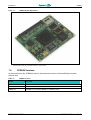
CPB904
ETX
AMD Geode LX 800 Based
Computer-on-Module
User Manual
Rev. 001 E
March 2008
P
r
e
l
i
m
i
n
a
r
y
Product Title:
CPB904
Document name: CPB904 User Manual
Manual version: 001 E
Copyright © 2008 Fastwel Co. Ltd. All rights reserved.
Revision Record
Rev. Index
Brief Description of Changes
Board Index
Date of Issue
001
Initial preliminary version
CPB904, KIB1282
March 2008
Contact Information
Fastwel Co. Ltd
Fastwel Corporation US
Address:
108 Profsoyuznaya st.,
Moscow 117437,
Russian Federation
45 Main Street
Suite 319
New York, 11201 USA
Tel.:
+7 (495) 232-1681
+1 (718) 554-36-86
Fax:
+7 (495) 232-1654
+1 (718) 797-06-00
E-mail:
[email protected]
mailto:[email protected]
Web:
http://www.fastwel.com/
CPB904
Table of Contents
Table of Contents.................................................................................................................................................. 0-1
List of Tables......................................................................................................................................................... 0-2
List of Figures ....................................................................................................................................................... 0-2
Notation Conventions............................................................................................................................................ 0-3
General Safety Precautions .................................................................................................................................. 0-4
Unpacking, Inspection and Handling..................................................................................................................... 0-5
Three Year Warranty ............................................................................................................................................ 0-7
1
Introduction......................................................................................................................................... 1-1
1.1
1.2
1.3
1.4
2
Technical Specifications ................................................................................................................... 2-1
2.1
2.2
2.3
2.4
2.5
2.6
3
General...................................................................................................................................................... 2-1
Power Requirements ................................................................................................................................. 2-2
Environmental............................................................................................................................................ 2-3
Mechanical ................................................................................................................................................ 2-3
Dimensions and Weight............................................................................................................................. 2-3
MTBF......................................................................................................................................................... 2-3
External Connections ........................................................................................................................ 3-1
3.1
3.2
3.3
4
Module Introduction ................................................................................................................................... 1-1
CPB904 Versions ...................................................................................................................................... 1-2
Delivery Checklist ...................................................................................................................................... 1-3
Supplementary Information........................................................................................................................ 1-3
1.4.1
Related Documents .................................................................................................................. 1-3
Safety Regulations..................................................................................................................................... 3-1
Connection of Peripheral Devices.............................................................................................................. 3-2
Software Installation .................................................................................................................................. 3-2
Functional Description ...................................................................................................................... 4-1
4.1
4.2
4.3
C P B 9 0 4
Structure and Layout ................................................................................................................................. 4-1
Address Mapping....................................................................................................................................... 4-4
4.2.1
Memory Addressing .................................................................................................................. 4-4
4.2.2
I/O Addressing .......................................................................................................................... 4-4
4.2.3
Interrupt settings ....................................................................................................................... 4-5
4.2.4
DMA Channels.......................................................................................................................... 4-6
Functional Description ............................................................................................................................... 4-6
4.3.1
Microprocessor ......................................................................................................................... 4-6
4.3.2
SDRAM Memory....................................................................................................................... 4-6
4.3.3
PCI and ISA Buses ................................................................................................................... 4-6
4.3.4
Reserved Flash BIOS ............................................................................................................... 4-7
4.3.5
UIDE Interface .......................................................................................................................... 4-7
4.3.6
NAND Flash.............................................................................................................................. 4-7
4.3.7
MiniSD Socket .......................................................................................................................... 4-7
4.3.8
Video Controller and Connection of Monitors ........................................................................... 4-8
4.3.9
Audio Controller ........................................................................................................................ 4-8
4.3.10
Watchdog Timer and Power Votage Monitoring ....................................................................... 4-8
4.3.11
PS/2 Keyboard and Mouse Interface ........................................................................................ 4-8
4.3.12
USB Interface ........................................................................................................................... 4-8
U s e r
M a n u a l
0-1
© 2 0 0 8
F a s t w e l
v .
0 0 1
E
CPB904
4.3.13
Fast Ethernet Interface ............................................................................................................. 4-9
4.3.14
Serial Ports ............................................................................................................................... 4-9
4.3.15
FDD/LPT Port ........................................................................................................................... 4-9
4.3.16
RTC and Serial FRAM .............................................................................................................. 4-9
4.3.17
LED Indicator ............................................................................................................................ 4-9
4.3.18
Discrete Input/Output .............................................................................................................. 4-10
4.3.19
Power Supply Connector ........................................................................................................ 4-10
4.3.20
ETX Connectors ..................................................................................................................... 4-10
Overall and Mounting Dimensions ........................................................................................................... 4-13
4.4
5
General Software® BIOS ................................................................................................................... 5-1
5.1
BIOS Setup Program. Introduction ............................................................................................................ 5-1
List of Tables
Table 1.1:
Table 1.2:
Table 1.3:
Table 4.1:
Table 4.2:
Table 4.3:
Table 4.4:
Table 4.5:
Table 4.6:
Table 4.7:
Table 4.8:
CPB904 Versions ...................................................................................................................................... 1-2
CPB904 Supplied Set ................................................................................................................................ 1-3
Related Publications .................................................................................................................................. 1-3
Memory Address Mapping......................................................................................................................... 4-4
I/O Address Space..................................................................................................................................... 4-4
Interrupt Settings ....................................................................................................................................... 4-5
DMA Request Map .................................................................................................................................... 4-6
X1 ETX Connector Pinout........................................................................................................................ 4-10
X2 ETX Connector Pinout........................................................................................................................ 4-11
X3 ETX Connector Pinout........................................................................................................................ 4-11
X4 ETX Connector Pinout........................................................................................................................ 4-12
List of Figures
Figure 1.1:
Figure 3.1:
Figure 4.1:
Figure 4.2:
Figure 4.3:
Figure 4.4:
CPB904 Module Appearance .................................................................................................................... 1-2
KIB1282 Baseboard Appearance .............................................................................................................. 3-2
CPB904 Block Diagram ............................................................................................................................. 4-1
Top Side: Connectors and Main Components Layout ............................................................................... 4-3
Bottom Side: Connectors and Main Components Layout .......................................................................... 4-3
CPB904 Top Side: Overall and Mounting Dimensions ............................................................................ 4-13
All information in this document is provided for reference only, with no warranty of its suitability for any specific purpose. This
information has been thoroughly checked and is believed to be entirely reliable and consistent with the product that it describes.
However, Fastwel accepts no responsibility for inaccuracies, omissions or their consequences, as well as liability arising from
the use or application of any product or example described in this document.
Fastwel Co. Ltd. reserves the right to change, modify, and improve this document or the products described in it, at Fastwel's
discretion without further notice. Software described in this document is provided on an “as is” basis without warranty. Fastwel
assumes no liability for consequential or incidental damages originated by the use of this software.
This document contains information, which is property of Fastwel Co. Ltd. It is not allowed to reproduce it or transmit by any
means, to translate the document or to convert it to any electronic form in full or in parts without antecedent written approval of
Fastwel Co. Ltd. or one of its officially authorized agents.
Fastwel and Fastwel logo are trademarks owned by Fastwel Co. Ltd., Moscow, Russian Federation. Ethernet is a registered
trademark of Xerox Corporation. IEEE is a registered trademark of the Institute of Electrical and Electronics Engineers Inc.
Intel is a trademark of Intel Corporation. Geode is trademark of AMD. ETX and ETXexpress are trademarks or registered
trademarks of Kontron Embedded Modules GmbH. Microsoft is a trademark of the Microsoft corporation. In addition, this
document may include names, company logos and trademarks, which are registered trademarks and, therefore,
are property of their respective owners.
Fastwel welcomes suggestions, remarks and proposals regarding the form and the content of this Manual.
C P B 9 0 4
U s e r
M a n u a l
0-2
© 2 0 0 8
F a s t w e l
v .
0 0 1
E
CPB904
Notation Conventions
Warning, ESD Sensitive Device!
This symbol draws your attention to the information related to electro static sensitivity of your
product and its components. To keep product safety and operability it is necessary to handle
it with care and follow the ESD safety directions.
Warning!
This sign marks warnings about hot surfaces. The surface of the heatsink and some
components can get very hot during operation. Take due care when handling, avoid
touching hot surfaces!
Caution: Electric Shock!
This symbol warns about danger of electrical shock (> 60 V) when touching products or
parts of them. Failure to observe the indicated precautions and directions may expose your
life to danger and may lead to damage to your product.
Warning!
Information marked by this symbol is essential for human and equipment safety.
Read this information attentively, be watchful.
Note...
This symbol and title marks important information to be read attentively for your own benefit.
C P B 9 0 4
U s e r
M a n u a l
0-3
© 2 0 0 8
F a s t w e l
v .
0 0 1
E
CPB904
General Safety Precautions
This product was developed for fault-free operation. Its design provides conformance to all related
safety requirements. However, the life of this product can be seriously shortened by improper
handling and incorrect operation. That is why it is necessary to follow general safety and
operational instructions below.
Warning!
All operations on this device must be carried out by sufficiently
skilled personnel only.
Warning!
When handling this product, special care must be taken not to hit
the heatsink (if installed) against another rigid object. Also, be
careful not to drop the product, since this may cause damage
to the heatsink, CPU or other sensitive components as well.
Please, keep in mind that any physical damage to this product
is not covered under warranty.
Note:
This product is guaranteed to operate within the published
temperature ranges and relevant conditions. However, prolonged
operation near the maximum temperature is not recommended by
Fastwel or by electronic chip manufacturers due to thermal stress
related failure mechanisms. These mechanisms are common to all
silicon devices, they can reduce the MTBF of the product by
increasing the failure probability. Prolonged operation at the lower
limits of the temperature ranges has no limitations.
Caution, Electric Shock!
Before installing this product into a system and before installing
other devices on it, always ensure that your mains power is switched
off.
Always disconnect external power supply cables during all handling
and maintenance operations with this module to avoid serious
danger of electrical shock.
C P B 9 0 4
U s e r
M a n u a l
0-4
© 2 0 0 8
F a s t w e l
v .
0 0 1
E
CPB904
Unpacking, Inspection and Handling
Please read the manual carefully before unpacking the module or mounting the device into your
system. Keep in mind the following:
ESD Sensitive Device!
Electronic modules and their components are sensitive to static
electricity. Even a non-perceptible by human being static discharge
can be sufficient to destroy or degrade a component's operation!
Therefore, all handling operations and inspections of this product
must be performed with due care, in order to keep product integrity
and operability:
Preferably, unpack or pack this product only at EOS/ESD safe workplaces. Otherwise, it is
important to be electrically discharged before touching the product. This can be done by
touching a metal part of your system case with your hand or tool. It is particularly important
to observe anti-static precautions when setting jumpers or replacing components.
If the product contains batteries for RTC or memory back-up, ensure that the module is not
placed on conductive surfaces, including anti-static mats or sponges. This can cause shortcircuit and result in damage to the battery and other components.
Store this product in its protective packaging while it is not used for operational purposes.
Unpacking
The product is carefully packed in an antistatic bag and in a carton box to protect it against
possible damage and harmful influence during shipping. Unpack the product indoors only at a
temperature not less than +15°C and relative humidity not more than 70%. Please note, that if the
product was exposed to the temperatures below 0°С for a long time, it is necessary to keep it at
normal conditions for at least 24 hours before unpacking. Do not keep the product close to a heat
source.
Following ESD precautions, carefully take the product out of the shipping carton box. Proper
handling of the product is critical to ensure correct operation and long-term reliability. When
unpacking the product, and whenever handling it thereafter, be sure to hold the module preferably
by the front panel, card edges or ejector handles. Avoid touching the components and connectors.
Retain all original packaging at least until the warranty period is over. You may need it for
shipments or for storage of the product.
Initial Inspection
Although the product is carefully packaged, it is still possible that shipping damages may occur.
Careful inspection of the shipping carton can reveal evidence of damage or rough handling. Should
you notice that the package is damaged, please notify the shipping service and the manufacturer
as soon as possible. Retain the damaged packing material for inspection.
After unpacking the product, you should inspect it for visible damage that could have occurred
during shipping or unpacking. If damage is observed (usually in the form of bent component leads
or loose socketed components), contact Fastwel's official distributor from which you have
purchased the product for additional instructions. Depending on the severity of the damage, the
product may even need to be returned to the factory for repair. DO NOT apply power to the product
if it has visible damage. Doing so may cause further, possibly irreparable damage, as well as result
in a fire or electric shock hazard.
C P B 9 0 4
U s e r
M a n u a l
0-5
© 2 0 0 8
F a s t w e l
v .
0 0 1
E
CPB904
If the product contains socketed components, they should be inspected to make sure they are
seated fully in their sockets.
Handling
In performing all necessary installation and application operations, please follow only the
instructions supplied by the present manual.
In order to keep Fastwel’s warranty, you must not change or modify this product in any way, other
than specifically approved by Faswel or described in this manual.
Technical characteristics of the systems in which this product is installed, such as operating
temperature ranges and power supply parameters, should conform to the requirements stated by
this document.
Retain all the original packaging, you will need it to pack the product for shipping in warranty cases
or for safe storage. Please, pack the product for transportation in the way it was packed by the
supplier.
When handling the product, please, remember that the module, its components and connectors
require delicate care. Always keep in mind the ESD sensitivity of the product.
C P B 9 0 4
U s e r
M a n u a l
0-6
© 2 0 0 8
F a s t w e l
v .
0 0 1
E
CPB904
Three Year Warranty
Fastwel Co. Ltd. (Fastwel), warrants that its standard hardware products will be free from defects
in materials and workmanship under normal use and service for the currently established warranty
period. Fastwel’s only responsibility under this warranty is, at its option, to replace or repair any
defective component part of such products free of charge.
Fastwel neither assumes nor authorizes any other liability in connection with the sale, installation
or use of its products. Fastwel shall have no liability for direct or consequential damages of any
kind arising out of sale, delay in delivery, installation, or use of its products.
If a product should fail through Fastwel's fault during the warranty period, it will be repaired free of
charge. For out of warranty repairs, the customer will be invoiced for repair charges at current
standard labor and materials rates.
Warranty period for Fastwel products is 36 months since the date of purchase.
The warranty set forth above does not extend to and shall not apply to:
1.
Products, including software, which have been repaired or altered by other than
Fastwel personnel, unless Buyer has properly altered or repaired the products in
accordance with procedures previously approved in writing by Fastwel.
2.
Products, which have been subject to power, supply reversal, misuse, neglect,
accident, or improper installation.
Returning a product for repair
1.
Apply to Fastwel company or to any of the Fastwel's official representatives for the
Product Return Authorization.
2.
Attach a failure inspection report with a product to be returned in the form, accepted by
customer, with a description of the failure circumstances and symptoms.
3.
Carefully package the product in the antistatic bag, in which the product had been
supplied. Failure to package in antistatic material will VOID all warranties. Then
package the product in a safe container for shipping.
4.
The customer pays for shipping the product to Fastwel or to an official Fastwel
representative or dealer.
C P B 9 0 4
U s e r
M a n u a l
0-7
© 2 0 0 8
F a s t w e l
v .
0 0 1
E
Introduction
1
CPB904
Introduction
This document presents general information on CPB904 processor module, the details of its proper
and safe installation, configuration and operation.
1.1
Module Introduction
CPB904 is an ETX computer-on-module (COM), highly integrated and compact single board
computer for use in systems requiring low power consumption and wide operating temperature
range. All I/O signals as well as full realization of ISA and PCI buses are mapped to four standard
high density, low profile connectors on the bottom side of the module. CPB904 is designed for use
in applications being mounted on an ETX baseboard.
CPB904 is based on low power AMD Geode LX800 CPU and AMD CS5536AC I/O companion.
Dynamic Memory interface supports 64-bit DDR SDRAM via SODIMM socket and soldered 128 or
256 MB memory bank.
All key components including CPU, chipset, memory, and periphery controllers are soldered
on-board providing excellent vibration stability and increased efficiency of protective conformal
coating.
CPB904 offers wide variety of data display capabilities. It allows simultaneous operation of
standard VGA interface, 24-bit LVDS interface, and 18-bit interface for TFT or DSTN LCD panels
connection. In addition TV output is available.
Data storage subsystem is based on single-channel IDE controller, that is able to drive up to two
IDE devices: two external hard drives, CompactFlash card.
For data exchange, CPB904 uses one independent Fast Ethernet port, three COM ports, four USB
2.0 ports, IrDA port, and parallel port combined with FDD and with 17 programmable discrete
input/output lines.
System control and management capabilities of CPB904 include watchdog timer, reserved BIOS,
and possibility to save system configuration and emergency parameters in FRAM chip.
CPB904 is manufactured in three versions: CPB904-01 (256 MB of soldered system memory),
CPB904-02 (512 MB soldered), and CPB904-03 with SODIMM socket for up to 512 MB DDR
SDRAM.
CPB904 is designed for operation within industrial temperature range from –40 C to +85°C.
CPB904 supports wide range of operating systems – Fastwel DOS (MS DOS-compatible),
Windows XP embedded, QNX 4.25 and 6.3x, Linux 2.4, and Windows CE.NET 4.2.
C P B 9 0 4
U s e r
M a n u a l
1-1
© 2 0 0 8
F a s t w e l
v .
0 0 1
E
Introduction
CPB904
Figure 1.1:
CPB904 Module Appearance
The appearance may vary for different versions of the module.
1.2
CPB904 Versions
At the present time the CPB904 module is manufactured in three versions differing in system
memory size.
Table 1.1:
CPB904 Versions
Version
Decimal ID
CPB904-01
256 MB DDR SDRAM soldered memory
CPB904-02
512 MB DDR SDRAM soldered memory
CPB904-03
SODIMM socket for DDR SDRAM, no soldered memory
C P B 9 0 4
U s e r
M a n u a l
1-2
© 2 0 0 8
F a s t w e l
v .
0 0 1
E
Introduction
1.3
CPB904
Delivery Checklist
Table 1.2:
CPB904 Supplied Set
Code
Description
Note
CPB904-01
CPB904-02
CPB904-03
Processor module
–
CD ROM with documentation and service software
Antistatic bag and consumer carton box
Note:
Keep the antistatic bag and the original package at least until the warranty period
is over. It can be used for future storage or warranty shipments.
1.4
Supplementary Information
1.4.1
Related Documents
Information related to this product and its components can be found in the following documents:
Table 1.3:
Related Publications
Product
Publication
CompactFlash cards
CF+ and CompactFlash Specification Revision 1.4
Processor
AMD Geode™ LX Processor Reference Schematic
AMD Geode™ LX Processors Data Book
AMD Geode™ CS5536 Companion Device Preliminary Data Book
AMD Geode™ LX Processor and CS5535/CS5536 Companion Devices
Layout Recommendations
Super I/O
Winbond W83627HF SuperIO Data sheet
C P B 9 0 4
U s e r
M a n u a l
1-3
© 2 0 0 8
F a s t w e l
v .
0 0 1
E
Technical Specifications
CPB904
2
Technical Specifications
2.1
General
CPU: AMD Geode LX800 500 MHz
32-bit x86/x87 compatible core
64-bit coprocessor
64-bit memory bus, up to 400 MHz
64 KB L1, 128 KB L2 cache
Integrated FPU supports the Intel MMX™ and AMD 3DNow!™ Technology
instruction sets
System memory
256 or 512 MB soldered SDRAM
DDR333
Up to 512 MB in SODIMM socket (for CPB904-03)
Flash BIOS
2x512 KB, reserved
In-system modification
Storage:
Support for up to two UltraDMA-100 IDE devices
Solid state disk: soldered, 64 MB NAND flash, with
MS DOS-compatible Fastwel file system
MiniSD socket on board
CompactFlash (via KIB1282)
Serial ports
Three serial ports
High speed 16C550 compatible
COM1, COM2: RS232, 9 wires, up to 115.2 Kb/s
COM3: RS232, TX/RX, for remote PC connection
USB
Four USB 2.0 channels
Ethernet
One Fast Ethernet port 10/100 Mb/s
C P B 9 0 4
U s e r
M a n u a l
2-1
© 2 0 0 8
F a s t w e l
v .
0 0 1
E
Technical Specifications
CPB904
Video controller
2D accelerator
Video memory 64 MB shared with system
LCD (TFT or DSTN) panels support, resolution up to 1600×1200 at 60 Hz
18-bit color via TFT interface, 24-bit color via LVDS
Analog display support,
resolution 1600×1200 at 100 Hz, 1920×1440 at 85 Hz, 32-bit
LVDS interface
Discrete I/O
17 discrete I/O lines, shared with LPT port
Watchdog timer
Fixed timeout period 1.6 s
Safety
System configuration settings stored in CMOS+SFRAM
Saving essential user data in SFRAM in case of power failure
CPU temperature and voltages monitoring
RTC
On-board real time clock with Li battery on baseboard
PS/2
PS/2 keyboard and mouse interface
FDD
Floppy disk interface
Parallel port
SPP/ECP/EPP compatible. Lines, shared with FDD controller
Expansion Buses
32-bit PCI
16-bit ISA
X1-X4 ETX headers
Software Support:
General Software® BIOS
Fastwel DOS, Windows XP Embedded, QNX® 4.25 and 6.3x, Linux® 2.4,
Windows CE.NET 4.2
2.2
Power Requirements
The module is powered via X1-X4 ETX connectors by an external DC power source providing the
following characteristics:
Voltage: +5 V ±5% (from +4.75 V to +5.25 V)
Consumption current (without external devices): 1.2 A
Note:
+5 V SB voltage is used in testing mode. +5 V voltage may be
supplied via J6 connector while testing the module
C P B 9 0 4
U s e r
M a n u a l
2-2
© 2 0 0 8
F a s t w e l
v .
0 0 1
E
Technical Specifications
2.3
CPB904
Environmental
Operating temperature range from: -40°C to +85°C
Storage temperature: -55°C to +90°C
Relative humidity: 5% to 95% at 25°С, noncondensing
2.4
Mechanical
Vibration – TBD;
Single shock, peak acceleration – TBD;
Multiple shock, peak acceleration – TBD.
2.5
Dimensions and Weight
Dimensions, not more: 114 × 95 × 11.4 mm (4.5” × 3.7” × 0.45”)
Weight, not more:
~0.1 kg (TBD later)
(without SODIMM memory module and MiniSD card)
2.6
MTBF
MTBF for CPB904 is 200000 hours
The value is calculated according to: Telcordia Issue 1 model, Method I Case 3, for continuous operation
at a surface location, at normal environmental conditions (Russian State Standard GOST 15150-69,
"UHL4" climatic parameters) and at ambient temperature 30°С.
C P B 9 0 4
U s e r
M a n u a l
2-3
© 2 0 0 8
F a s t w e l
v .
0 0 1
E
External Connections
3
CPB904
External Connections
The following precautions must be observed to ensure proper installation and to avoid damage to
the module, other system components, or harm to personnel.
3.1
Safety Regulations
The following safety regulations must be observed when installing or operating the module.
Fastwel assumes no responsibility for any damage resulting from infringement of these rules.
Warning!
When handling or operating the module, special attention should be
paid to the heatsink, because it can get very hot during operation.
Do not touch the heatsink when installing or removing the module.
Moreover, the module should not be placed on any surface or in any
kind of package until the module and its heatsink have cooled down
to ambient temperature.
ESD Sensitive Equipment!
This product comprises electrostatically sensitive components.
Please follow the ESD safety instructions to ensure module's
oparability and reliability:
Use grounding equipment, if working at an anti-static
workbench. Otherwise, discharge yourself and the tools
in use before touching the sensitive equipment.
Try to avoid touching contacts, leads and components.
Extra caution should be taken in cold and dry weather.
C P B 9 0 4
U s e r
M a n u a l
3-1
© 2 0 0 8
F a s t w e l
v .
0 0 1
E
External Connections
3.2
CPB904
Connection of Peripheral Devices
External devices, except for MiniSD cards, are connected to CPB904 via KIB1282 ATX carrier
board for ETX/XTX computer modules.
Figure 3.1:
KIB1282 Baseboard Appearance
The appearance may vary for different versions of the module.
KIB1282 baseboard provides access to the following interfaces and connectors:
VGA (D-Sub connector), S-Video, LVDS, FastEthernet 10/100-BaseT (one RJ45 connector),
two x1 PCI Express connectors, one 16-bit ISA and two PCI headers, USB 2.0 (four Type A
connectors), IDE UltraATA, four standard SATA connectors, CF Type I/II socket with IDE interface,
two RS232 COM ports, LPT and FDD standard connectors, two PS/2 connectors, two
ExpressCard™ slots, Audio line in/out, HD (5+1 out) Audio Codec, two MIC, IrDA, LPC interface,
SMBUS, PLCC, fan connector, control&signalling interfaces and LEDs, ATX power supply header.
3.3
Software Installation
Operating system is loaded from the on-board NAND Flash memory by default. Operating system
on this flash-disk is FDOS supplemented with utilities.
The installation of the peripheral drivers is described in the accompanying information files. For
details on installation of an operating system, please refer to the relevant software documentation.
C P B 9 0 4
U s e r
M a n u a l
3-2
© 2 0 0 8
F a s t w e l
v .
0 0 1
E
Functional Description
CPB904
4
Functional Description
4.1
Structure and Layout
Functional diagram of the CPB904 module is shown in Figure 4.1.
CPB904 Block Diagram
CRT
TFT LCD
(18-bit)
Out to
ETX CON
AMD Geode
LX800
Processor
TFT
Memory
Bus
ISA
Out to
ETX CON
SODIMM200 DDR
CRT
Out to
ETX CON
256/512 MB
DDR DRAM
Figure 4.1:
PCI to ISA
(IT8888)
VCORE (1.2 V)
VCCMEM (2.5 V)
+5V
ETX_VCC3 (3.3 V)
DC/DC
PCI Bus (33MHz or 66MHz)
VCC3SB (3.3 V)
PCI
Out to
ETX CON
VCORE SB
+5VSB
IDE
Out to
ETX CON
Primary IDE
USB x 4
Out to
ETX CON
USB 2.0 & OTG
ATA-66
10/100 Mb/s
Ethernet
Ethernet
Out to
ETX CON
AC97
Codec
Audio
In/Out to
ETX CON
South Bridge
(CS5536)
Geode
Companion
Device
COM3
14.318 MHz
Crystal
PCI (33/66 MHz)
Clock
Synthesizer
66 MHz
LPC Bus
48 MHz
(MK1491-09F)
REFCLK
C P B 9 0 4
U s e r
M a n u a l
Flash BIOS
SUPER I/O
(SST FWH)
(W83627HF)
4-1
COM 1,2
LPT/FDD
KB/MS
© 2 0 0 8
F a s t w e l
Out to
ETX CON
v .
0 0 1
E
Functional Description
CPB904
CPB904 includes the following main functional units:
AMD Geode LX 800 500 MHz microprocessor including 32-bit x86 core,
64-bit coprocessor, 64-bit SDRAM memory bus;
256/512 MB soldered DDR SDRAM system memory,
up to 512 MB in SODIMM socket (for CPB904-03);
Flash memory based reserved BIOS, in-system modification;
Onboard NAND flash-disk, 64 MB;
IDE port with support for two UltraDMA/100 devices;
MiniSD socket;
Serial ports:
COM1, COM2: RS232, full control, maximum exchange rate – 115.2 Kbit/s;
COM3: RS232, TX/RX, for remote PC connection
One Fast Ethernet channel 10/100 Mbit/s;
Four USB 2.0 channels;
Watchdog timer;
CMOS+SFRAM for BIOS configuration storage;
Real time clock with Li battery backup;
PS/2 keyboard/mouse port;
IrDA port;
17 programmable discrete I/O channels share lines with FDD/LPT ports.
Universal parallel port supports EPP and ECP modes;
Integrated graphics controller:
Video memory up to 64 MB, shared with system;
LCD (TFT or DSTN) panels support, resolution up to 1600x1200;
Analog RGB display support;
LVDS interface
Layouts of main CPB904 components and connectors on top and bottom sides are presented in
Figures 4.2 and 4.3 respectively.
C P B 9 0 4
U s e r
M a n u a l
4-2
© 2 0 0 8
F a s t w e l
v .
0 0 1
E
Functional Description
Figure 4.2:
CPB904
Top Side: Connectors and Main Components Layout
necto
e Con
Servic
R
C OM3
S232
M
SOD IM
2)
ket (J
D Soc
MiniS
(J4)
ridge
ISA B
PCI to ator
dic
)
LED In tton (SW1
u
B
t
e
s
Re
rbiter
PCI A BIOS
ry
a
Prim
6
3
CS55
c
Code
Audio
(J1)
ector
Conn
e
ic
rv
Se
(J9)
er
ontroll
n e t C o we r
Aux P 5)
(J
5VSB
to
5V
CP U
X800
ode L
Ether
Ge
AMD
I/O
Super
V Con
RGB/T
r (J3)
verter
The layout may slightly differ for various versions of the board.
Figure 4.3:
Bottom Side: Connectors and Main Components Layout
DDR
M
SDR A
XC
X4 ET
r
necto
X Co n
T
E
2
X
k
sh Dis
el Fla
Fastw
CPLD
to
onnec
r
necto
r
X Con
X3 ET
r
necto
X Co n
X1 ET
S
rve BIO
Rese
LVDS itter/
m
Trans rter
Conve
FRAM
Clock
rator
n
e
G e
The layout may slightly differ for various versions of the board.
C P B 9 0 4
U s e r
M a n u a l
4-3
© 2 0 0 8
F a s t w e l
v .
0 0 1
E
Functional Description
CPB904
4.2
Address Mapping
4.2.1
Memory Addressing
Table 4.1:
Memory Address Mapping
Address Range
Size
Description
00000h – 09FFFh
640 KB
System memory
A0000h – BFFFFh
128 KB
Video memory
C0000h – С7FFFh
32 KB
Display BIOS memory or external bus memory
C8000h – DBFFFh
80 KB
External bus memory
DC000h – DFFFFh
16 KB
SMI handler
E0000h – FFFFFh
128 KB
System BIOS area
100000h – FFFFFFFh
255 MB
Extended system memory
FFFFFFFFh – 10007FFFFh
512 KB
ROM BIOS area
4.2.2
I/O Addressing
Table 4.2:
I/O Address Space
Address Range
Function
Note
0000h – 001Fh
DMA1
–
0020h – 0021h
PIC master
–
0022h – 0023h
LX configuration
–
0028h – 002Fh
Local bus
–
0040h – 005Fh
Timer
–
0060h – 006Fh
POST, keyboard shadow registers
–
0070h – 007Fh
CMOS, NMI mask control registers
–
0080h – 009Fh
DMA page registers
–
00A0h – 00BFh
Slave PIC
–
00C0h – 00DFh
DMA2
–
00F0h – 00FFh
Numeric coprocessor
–
0100h – 016Fh
External 16-bit ISA bus
External bus access
0170h – 0177h
Reserved
–
0180h – 01EFh
External 16-bit ISA bus
External bus access
01F0h – 01F7h
Primary IDE
–
0200h – 020Ah
External 16-bit ISA bus
External bus access
020Bh – 020Fh
CPB904 control registers
–
0210h – 026Fh
External 16-bit ISA bus
External bus access
0270h – 027Fh
Reserved
–
0280h – 02E7h
External 16-bit ISA bus
External bus access
02E8h – 02EFh
Reserved
–
C P B 9 0 4
U s e r
M a n u a l
4-4
© 2 0 0 8
F a s t w e l
v .
0 0 1
E
Functional Description
CPB904
Address Range
Function
Note
02F8h – 02FFh
COM2
RS232
0300h – 0301h
CPB904 FFD
–
0302h – 036Fh
External 16-bit ISA bus
External bus access
0370h – 0377h
Reserved
–
0378h – 037Fh
LPT1
–
0380h – 03AFh
Reserved
–
03B0h – 03DFh
EGA, VGA, CGA
–
03E8h – 03EFh
COM3
RS232
03F0h – 03F75h
FDD Controller
–
03F8h – 03FFh
COM1
RS232
0400h – FFFFh
External 16-bit ISA bus
External bus access
0CF8h – 0CFFh
Host PCI controller configuration registers
–
4.2.3
Interrupt settings
Table below presents interrupt settings. Interrupt request configuration is performed in BIOS Setup.
Table 4.3:
Interrupt Settings
IRQ
Source
IRQ0
System timer
IRQ1
Keyboard
IRQ2
8259 interrupt
IRQ3
COM2
IRQ4
COM1
IRQ5
Ethernet / USB / Audio
IRQ6
FDD
IRQ7
LPT
IRQ8
RTC
IRQ9
Ethernet / USB / Audio
IRQ10
Free
IRQ11
Free
IRQ12
Mouse
IRQ13
Reserved for math. coprocessor
IRQ14
HDD, CompactFlash
IRQ15
COM3
C P B 9 0 4
U s e r
M a n u a l
4-5
© 2 0 0 8
F a s t w e l
v .
0 0 1
E
Functional Description
4.2.4
CPB904
DMA Channels
Table 4.4:
DMA Request Map
DMA Channel
Main Function
Alternative Source
0
Reserved
–
1
LPT
DRQ1 line of external ISA bus
2
FDD
–
3
DRQ3 line of external ISA bus
–
4
Slave controller
–
5
–
–
6
–
–
7
–
–
4.3
Functional Description
4.3.1
Microprocessor
The module is based on AMD Geode LX800 microprocessor with 1.8W typical power consumption
at 500 MHz, maximum power 3.6W (TDP). The processor includes 32-bit x86 core, 64-bit
coprocessor and 64-bit DDR memory bus up to 400 MHz, graphics and video controller with VGA
monitors and LCD panels simultaneous operation support. FPU of the processor supports MMX™
and AMD 3DNow!™ technology instruction sets. The CPU is complemented with AMD Geode
CS5536 companion device providing support for numerous I/O functions including IDE, USB,
audio, and power management interfaces.
4.3.2
SDRAM Memory
Four DDR 333 SDRAM memory chips are soldered on the bottom side of the PCB. Total memory
size is 256 or 512 MB depending on the version of the module. In addition, the module can accept
up to 512 MB of DDR SDRAM via SODIMM socket on the top side of the board (for CPB904-03).
4.3.3
PCI and ISA Buses
Expansion capabilities of CPB904 are supported by 32-bit PCI bus routed to X1 ETX connector.
Moreover, ITE IT8888G PCI-to-ISA bridge provides full-functional 16-bit ISA bus available via X2
ETX connector.
C P B 9 0 4
U s e r
M a n u a l
4-6
© 2 0 0 8
F a s t w e l
v .
0 0 1
E
Functional Description
4.3.4
CPB904
Reserved Flash BIOS
The CPB904 takes advantage of flash-memory based BIOS. Two Flash BIOS chips have storage
capacity of 512 KB each. The main (working) copy of BIOS occupies 512 KB on a chip in PLCC32
panel. Reserve BIOS copy is stored on a soldered chip and is used for emergency boot. Switching
to reserve BIOS copy is performed automatically.
It is possible to upgrade the main copy of BIOS in-system. It is done with the help of fwflash.exe
program. For example:
fwflash.exe b304v1_3.bin
where
b304v1_3.bin – BIOS image binary file name.
BIOS can be upgraded via RS232 (COM1) serial port in console operation mode. To do so,
connect COM ports of the module and of a remote PC, enable Start RS232 Manufacturing Link
mode in BIOS Setup, and run fwflash.exe utility at a remote PC with the following parameters:
fwflash.exe b304v1_3.bin 1
where
b304v1_3.bin – BIOS image binary file name
1 – PC COM port number (COM1)
4.3.5
UIDE Interface
CPB904 has one IDE ATA-5/ATAPI interface with support of PIO mode 0-4, MDMA mode 0-2,
UDMA mode 0-5 including UltraDMA100. It allows connection of two UDMA-100 compatible
devices (master and slave) to the primary IDE channel. External devices are connected to IDE
interface via HDD connector and CompactFlash type I/II socket located on KIB1282 carrier board.
4.3.6
NAND Flash
Capacity of the on-board NAND flash memory chip is 64 MB. It is available only under DOS,
Windows CE, and Linux operating systems. It can be used as a bootable disk or can be disabled in
BIOS Setup. Since only one IDE channel is used, it is possible to connect storage devices in one
of the ways described below.
Connection Variant
IDE-Master
IDE-Slave
CF-Master
CF-Slave
NAND Flash
1
+
+
–
–
+
2
+
–
–
+
+
3
–
+
+
–
+
Selection of disk drives operation mode (master of slave) is performed in BIOS Setup.
4.3.7
MiniSD Socket
CPB904 is equipped with a MiniSD socket, located on the top side of the module. It is not used in
current versions of the module.
C P B 9 0 4
U s e r
M a n u a l
4-7
© 2 0 0 8
F a s t w e l
v .
0 0 1
E
Functional Description
4.3.8
CPB904
Video Controller and Connection of Monitors
The module utilizes graphics controller integrated in Geode LX CPU with the following main
features:
Video memory size up to 64 MB shared with system;
Support of TFT or DSTN LCD-panels with resolution up to 1600×1200 at 18 bpp,
LVDS panels with resolution up to 1600×1200 at 24 bpp;
Support of VGA RGB monitors with resolution up to 1920×1440 (85 Hz, 32 bpp);
LVDS interface
CRT VGA monitors and/or LCD panels are connected to KIB1282 carrier board. Video interfaces
are routed to KIB1282 via X3 ETX connector. As an option, CPB904 can be equipped with TV
encoder chip providing TV Output function.
4.3.9
Audio Controller
AC'97 audio codec functions are performed by Realtek ALC203 chip incorporating two channel
20-bit DAC. Audio lines are routed to X1 ETX connector.
4.3.10
Watchdog Timer and Power Votage Monitoring
CPB904 has one watchdog timer with fixed timeout period of 1.6 s, which is controlled by CPLD.
Watchdog timer is in "on" state on power up. Watchdog timer operation modes are switched in
BIOS Setup program.
Power voltage monitoring and watchdog functions are performed by ADM706T supervisor chip.
+5V voltage is monitored. Reset signal is generated when +5V voltage goes down to +4.75V.
3.3 V can be monitored by Winbond W83627HF SuperIO chip using software utilities. Moreover,
this chip is also used to monitor CPU temperature by means of a sensor integrated in
microprocessor and board temperature using optional on-board sensor.
4.3.11
PS/2 Keyboard and Mouse Interface
PS/2 keyboard and mouse interface is routed to KIB1282 baseboard via X3 connector. Keyboard
and mouse are connected to separate connectors on the baseboard.
4.3.12
USB Interface
The module is equipped with four USB 2.0 host ports. All channels have power control circuit. One
USB device may be connected to each port. All channels are routed to KIB1282 baseboard via X1
ETX connector.
C P B 9 0 4
U s e r
M a n u a l
4-8
© 2 0 0 8
F a s t w e l
v .
0 0 1
E
Functional Description
4.3.13
CPB904
Fast Ethernet Interface
CPB904 has one 10Base-TX/100Base-TX Ethernet channel provided by Intel LU82551IT
controller. It is routed through X4 ETX header to KIB1282 baseboard, where Ethernet port is
available via RJ45 connector.
4.3.14
Serial Ports
The CPB904 is furnished with three serial ports having standard PC AT base addresses. Their
operation is provided by Winbond W83627HF Super I/O chip internal UARTs.
COM1 and COM2 (RS232) operate as full function 9-wire RS232 interfaces with maximum transfer
rate of 115.2 Kb/s. They are fully compatible with UART16550. Both COM1 and COM2 ports are
routed via X3 ETX connector to standard D-Sub connectors at KIB1282 baseboard.
COM3 is available via 3-pin 2 mm pitch connector (J4) mounted on the top side of CPB904
module. It is a dedicated connector for remote PC console operation, it transfers only RXD, TXD,
and GND lines. For communication with a remote PC (console operation) a null-modem cable is
needed.
4.3.15
FDD/LPT Port
Super I/O chip includes FDD controller and universal parallel port sharing the same lines routed via
X3 ETX connector to KIB1282 baseboard connectors. Switching between LPT and FDD ports is
performed in BIOS Setup. FDD port allows connection of one device. LPT port of CPB904 supports
EPP and ECP operation modes. ECP is the default mode.
LPT uses IRQ7 interrupt line, IRQ6 is assigned to FDD port. If "On-board LPT/FDC" parameter is
set to "Disabled" in BIOS Setup, IRQ7 and IRQ6 interrupts are available for user application.
4.3.16
RTC and Serial FRAM
The module is equipped with a standard Real Time Clock. FRAM is non-volatile memory with I2C
serial interface. It serves as a back-up storage for BIOS Setup parameters, for critical system
events information recording, and for restoration of the RTC memory if an error is detected. FRAM
write access is allowed for system software only.
In case of operating system crash and if BIOS Setup program can not be started, BIOS settings
can be reset using CMOS_RST.COM program. It is started under MS DOS 6.22 on a remote PC
connected to switched off CPB904 module with a null-modem cable via COM1 port. After this
procedure, BIOS settings are reset to default on module's power-up.
4.3.17
LED Indicator
CPB904 has a dual color programmable LED indicator on the top side of the module. Red light
turns into green on BIOS successful loading.
C P B 9 0 4
U s e r
M a n u a l
4-9
© 2 0 0 8
F a s t w e l
v .
0 0 1
E
Functional Description
4.3.18
CPB904
Discrete Input/Output
17 programmable input/output channels use FDD/LPT port lines.
4.3.19
Power Supply Connector
The power is supplied to CPB904 via ETX connectors in normal operation mode or via Aux Power
connector (J6) located on the top side of the module in module's test mode only. To enable
module's ability to be powered via J6 connector it is necessary to close pins on J5 pinpad. This
connects +5VSB voltage to module's +5V lines. Please, observe polarity while connecting wires to
J6 connector.
The main power voltage of the processor module is +5V. +3.3V voltage is generated onboard, it
may be used to power devices on baseboard with consumption current of up to 0.2 A.
4.3.20
ETX Connectors
CPB904 is equipped with four standard ETX low-profile 100-contact Hirose connectors to supply
module's interfaces to KIB1282 baseboard. The following four tables provide information on ETX
connectors contacts designation.
Table 4.5:
Pin#
1
2
3
4
5
6
7
8
9
10
11
12
13
14
15
16
17
18
19
20
21
22
23
24
25
X1 ETX Connector Pinout
Signal
GND
PCICLK3
PCICLK4
GND
PCICLK1
PCICLK2
–
–
–
+3.3V
–
GNT1#
REQ1#
+3.3V
GNT0#
USBPWREN1
+5V
SERIRQ
REQ0#
AD0
+3.3V
AD1
C P B 9 0 4
U s e r
M a n u a l
Pin#
Signal
Pin#
26
27
28
29
30
31
32
33
34
35
36
37
38
39
40
41
42
43
44
45
46
47
48
49
50
AD2
AD4
AD3
AD6
AD5
CBE0#
AD7
AD8
AD9
51
52
53
54
55
56
57
58
59
60
61
62
63
64
65
66
67
68
69
70
71
72
73
74
75
GND
AD10
AUXAL
AD11
MIC
AD12
AUXAR
AD13
VCC_AUD
AD14
SNDL
AD15
GND_AUD
CBE1#
SNDR
4-10
Signal
+5V
PAR
SERR#
PERR#
USBPWREN2
PME#
USB2#
LOCK#
DEVSEL#
TRDY#
USB3#
IRDY#
STOP#
FRAME#
USB2
GND
AD16
CBE2#
AD17
USB3
AD19
AD18
AD20
Pin#
Signal
76
77
78
79
80
81
82
83
84
85
86
87
88
89
90
91
92
93
94
95
96
97
98
99
100
USB0#
AD22
AD21
AD23
USB1#
AD24
CBE3#
© 2 0 0 8
+5V
AD25
AD26
AD28
USB0
AD27
AD29
AD30
USB1
PCIRST#
AD31
INTC#
INTD#
INTA#
INTB#
GND
F a s t w e l
v .
0 0 1
E
Functional Description
Table 4.6:
Pin#
1
2
3
4
5
6
7
8
9
10
11
12
13
14
15
16
17
18
19
20
21
22
23
24
25
X2 ETX Connector Pinout
Signal
GND
SD14
SD15
SD13
MASTER#
SD12
DREQ7
SD11
DACK7#
SD10
DREQ6
SD9
DACK6#
SD8
DREQ5
MEMW#
DACK5#
MEMR#
DREQ0
LA17
DACK0#
LA18
IRQ14
LA19
Table 4.7:
Pin#
1
2
3
4
5
6
7
8
9
10
11
12
13
14
15
16
17
18
19
20
21
22
23
24
25
Pin#
Signal
Pin#
26
27
28
29
30
31
32
33
34
35
36
37
38
39
40
41
42
43
44
45
46
47
48
49
50
IRQ15
LA20
IRQ12
LA21
IRQ11
LA22
IRQ10
LA23
IOCS16#
51
52
53
54
55
56
57
58
59
60
61
62
63
64
65
66
67
68
69
70
71
72
73
74
75
GND
SBHE#
MEMCS16#
SA0
OSC
SA1
BALE
SA2
TC
SA3
DACK2#
SA4
IRQ3
SA5
IRQ4
Signal
Pin#
Signal
IOW#
SA18
SA17
SA19
SMEMR#
IOCHRDY
AEN
SA13
DREQ3
SA14
DACK3#
SA15
IOR#
SA16
76
77
78
79
80
81
82
83
84
85
86
87
88
89
90
91
92
93
94
95
96
97
98
99
100
LPT_FLOPPY#
SEL66_33#
+5V
GND
STROBE# / –
AFD# / DENSEL
–
PD7 / DSA#
IRRX
ERR# / HDSEL#
IRTX
PD6 / MOTORA#
COM2_RXD
INIT# / DIR#
GND
GND
COM2_RTS#
PD5 / –
COM2_DTR#
SELIN# / STEP#
COM2_DCD#
PD4 / DSKCHG#
COM2_DSR#
PD3 / RDATA#
COM2_CTS#
76
77
78
79
80
81
82
83
84
85
86
87
88
89
90
91
92
93
94
95
96
97
98
99
100
+5V
SA6
IRQ5
SA7
IRQ6
SA8
IRQ7
SA9
SYSCLK
SA10
REFRESH#
SA11
DREQ1
SA12
DACK1#
GND
+5V
SD0
SMEMW#
SD2
SD1
SD3
NOWS#
DREQ2
SD4
SD5
IRQ9
SD6
SD7
IOCHK#
RSTDRV
GND
X3 ETX Connector Pinout
Signal
GND
RED
BLUE
HSYNC
GREEN
VSYNC
CRT_CLK
–
CRT_DAT
B4
DOTCLK / –
B5
LDEMOD / –
GND
GND
B1
B3
B0
B2
GND
GND
G2 / TX3#
G5
G3 / TX3
C P B 9 0 4
CPB904
U s e r
M a n u a l
Pin#
Signal
26
27
28
29
30
31
32
33
34
35
36
37
38
39
40
41
42
43
44
45
46
47
48
49
50
G4
GND
GND
R4 / TX2#
G1 / TCLK
R5 / TX2
G0 / TCLK#
GND
GND
R1 / TX0
R3 / TX1
R0 / TX0#
R2 / TX1#
+5V
+5V
–
–
–
DISPEN# / –
–
VDDEN / –
COMP
Y
–
C
51
52
53
54
55
56
57
58
59
60
61
62
63
64
65
66
67
68
69
70
71
72
73
74
75
4-11
© 2 0 0 8
PD2 / WP#
COM2_TXD
PD1 / TRK0#
COM2_RI#
PD0 / INDEX#
+5V
+5V
COM1_RXD
ACK# / DSB#
COM1_RTS#
BUSY/MOTORB#
COM1_DTR#
PE / WDATA#
COM1_DCD#
SLCT#/WE#
COM1_DSR#
MS_CLK
COM1_CTS#
MS_DAT
COM1_TXD
KB_CLK
COM1_RI#
KB_DAT
GND
F a s t w e l
v .
0 0 1
E
Functional Description
Table 4.8:
Pin#
1
2
3
4
5
6
7
8
9
10
11
12
13
14
15
16
17
18
19
20
21
22
23
24
25
X4 ETX Connector Pinout
Signal
GND
+5VCC_SB
–
PS_ON
SPEAKER
PWR_BTN#
BATTERY
RES_INMR#
LINK_LED#
SYS_RES#
ACT_LED#
USB_ID
SPEED_LED#
–
USB_VBUS
+5V
+5V
OVCR#
WORK_AUX
–
–
SMB_CLK
SMB_DAT
–
C P B 9 0 4
CPB904
U s e r
M a n u a l
Pin#
Signal
Pin#
Signal
Pin#
Signal
26
27
28
29
30
31
32
33
34
35
36
37
38
39
40
41
42
43
44
45
46
47
48
49
50
–
–
–
–
P_IDE_CS1#
–
P_IDE_CS0#
GND
GND
–
P_IDE_A2
–
P_IDE_A0
–
P_IDE_A1
–
–
–
P_IDE_INTRQ
–
P_IDE_ACK#
–
P_IDE_RDY
+5V
+5V
51
52
53
54
55
56
57
58
59
60
61
62
63
64
65
66
67
68
69
70
71
72
73
74
75
–
P_IDE_IOR#
–
P_IDE_IOW#
–
P_IDE_DRQ
–
P_IDE_D15
–
P_IDE_D0
–
P_IDE_D14
–
P_IDE_D1
GND
GND
–
P_IDE_D13
–
P_IDE_D2
–
P_IDE_D12
–
P_IDE_D3
–
76
77
78
79
80
81
82
83
84
P_IDE_D11
–
P_IDE_D4
–
P_IDE_D10
+5V
+5V
–
P_IDE_D5
–
P_IDE_D9
–
P_IDE_D6
–
CABLE_ID
ETH_RXD#
P_IDE_D8
ETH_RXD
–
ETH_TXD#
P_IDE_D7
ETH_TXD
HD_RST#
4-12
86
87
88
89
90
91
92
93
94
95
96
97
98
99
100
© 2 0 0 8
GND
F a s t w e l
v .
0 0 1
E
Functional Description
4.4
CPB904
Overall and Mounting Dimensions
Figure 4.4:
CPB904 Top Side: Overall and Mounting Dimensions
TBA
C P B 9 0 4
U s e r
M a n u a l
4-13
© 2 0 0 8
F a s t w e l
v .
0 0 1
E
General Software® BIOS
5
CPB904
General Software® BIOS
The General Software® BIOS in CPB904 is an adapted version of a standard BIOS for IBM PC
AT-compatible personal computers equipped with Intel®x86 and compatible processors. BIOS
provides low-level support for the central processing, memory, and I/O system units.
5.1
BIOS Setup Program. Introduction
With the BIOS Setup program, you can modify BIOS settings and control special features of the
module. The Setup program offers a convenient menu interface to modify basic system
configuration settings and switching between the subsystems operation modes. These settings are
stored in a dedicated battery-backed memory, CMOS RAM, that keeps the information when the
power is switched off.
C P B 9 0 4
U s e r
M a n u a l
5-1
© 2 0 0 8
F a s t w e l
v . 0 0 1
E