1
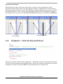
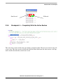
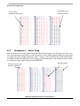
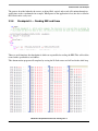
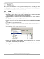
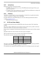
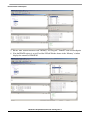
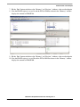
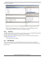
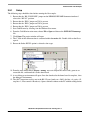
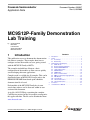
Freescale Semiconductor
Application Note
Document Number: AN3937
Rev. 0, 09/2009
MC9S12P-Family Demonstration
Lab Training
by: Gordon Borland
Matt Grant
Lela Garofolo
Steven McLaughlin
MSG Auto R & D
1
Introduction
This publication serves to document the demonstration
lab software examples. The examples show how to
configure and use the modules to users getting started
with the MC9S12P Family of MCUs.
Contents
1
2
3
The examples included here illustrate a basic
configuration of the modules to allow users to quickly
start developing their own applications.
Complete code is available for all examples. This can be
downloaded onto an MC9S12P128 target such as the
DEMO9S12PFAME demo board upon which this
demonstration lab is based.
Each module of the MC9S12P Family has its own
stand-alone software and is discussed within its own
section of this document.
A zip file, AN3937SW.zip, containing the complete
CodeWarrior projects for the lab examples accompanies
this application note. The file can be downloaded from
www.freescale.com.
© Freescale Semiconductor, Inc., 2009. All rights reserved.
4
5
Introduction . . . . . . . . . . . . . . . . . . . . . . . . . . . . . . . . . . . 1
Setup . . . . . . . . . . . . . . . . . . . . . . . . . . . . . . . . . . . . . . . . 2
2.1 Tools Setup . . . . . . . . . . . . . . . . . . . . . . . . . . . . . . . 2
2.2 Board Setup . . . . . . . . . . . . . . . . . . . . . . . . . . . . . . 2
Demonstration Lab Examples . . . . . . . . . . . . . . . . . . . . . 2
3.1 CPMU Clocks . . . . . . . . . . . . . . . . . . . . . . . . . . . . . 2
3.2 Flash Programming Example . . . . . . . . . . . . . . . . . 5
3.3 Emulated EEPROM Driver . . . . . . . . . . . . . . . . . . . 8
3.4
LIN Communications . . . . . . . . . . . . . . . . . . . . . . 14
3.5 MSCAN Module. . . . . . . . . . . . . . . . . . . . . . . . . . . 14
3.6 PWM Module . . . . . . . . . . . . . . . . . . . . . . . . . . . . . 16
3.7 S12P Low-Power Modes . . . . . . . . . . . . . . . . . . . . 17
3.8 MMC Program Flash Paging Window . . . . . . . . . 19
3.9 ADC Module . . . . . . . . . . . . . . . . . . . . . . . . . . . . . 24
3.10 Timer Module . . . . . . . . . . . . . . . . . . . . . . . . . . . . 26
3.11 SCI Communications . . . . . . . . . . . . . . . . . . . . . . 28
3.12 SPI Communications . . . . . . . . . . . . . . . . . . . . . . 29
Conclusion. . . . . . . . . . . . . . . . . . . . . . . . . . . . . . . . . . . 31
Useful Reference Material . . . . . . . . . . . . . . . . . . . . . . . 32
Setup
2
Setup
2.1
Tools Setup
NOTE
Before starting any of the module examples in this document, it is important
that you complete the Software Setup and Hardware Setup as described in
the DEMO9S12PFAME User’s Manual which accompanies the
demonstration board.
2.2
Board Setup
The steps listed below provide a basic configuration for each of the module examples in this document.
Any deviation from this basic configuration or any specific requirements for a module will be outlined in
the relevant module chapter.
1. Ensure that the RESET# and BKGD jumpers are present on the BDM ENA header.
2. Ensure that all of the SW ENA jumpers are present.
3. Ensure that all of the LED ENA jumpers are present.
4. Ensure that all of the CAN ENA jumpers are present.
5. Ensure that the LIN ENA jumper is present.
6. Ensure that the VDD CAN ENA jumper is present.
7. Ensure that the VAUX ENA jumper is present.
8. Ensure that the RS-232/LIN SEL jumpers select the RS-232 position.
9. Ensure that the POWER SEL jumper selects the USB position.
10. Connect the demonstration board to the PC via the USB cable.
11. The green POWER LED on the board should turn on.
3
Demonstration Lab Examples
3.1
CPMU Clocks
This lab example shows how to produce PLL-based bus clocks using the different clock modes of the
CPMU module. The example software initializes the PLL to run in default 8 MHz PEI mode, 12.5 MHz
PEI mode, 32 MHz PEE mode and 2 MHz PBE mode. The changes in bus clock can be observed via the
LED pulse rate and the frequency can be measured by monitoring the ECLK signal (Bus clock) on an
oscilloscope.
MC9S12P-Family Demonstration Lab Training, Rev. 0
2
Freescale Semiconductor
Demonstration Lab Examples
3.1.1
Setup
The following steps should be taken before running the lab example:
1. Start CodeWarriorTM by selecting it in the Windows Start menu.
2. From the CodeWarrior main menu, choose File > Open and choose the S12P System Clocks.mcp
file.
3. Click Open. The project window will open.
4. The C code of this demonstration is contained within the main.c file. Double click on the file to
open it.
5. Ensure the “Softec HCS12” option is selected as the target.
6. From the main menu choose Project > Debug. This will compile the source code, generate an
executable file, and download it to the demo board.
7. A new debugger environment will open. Once the download to the demo board is complete, close
the debugger environment.
8. Ensure that the RS-232/LIN SEL jumper on the DEMO9S12PFAME demonstration board selects
the RS-232 position.
9. The PLL configuration is sent to the RS-232 port (baud rate = 9600, data bits = 8, parity = N, stop
bits = 1, Flow control = Hardware). Open a terminal window on the PC with this configuration.
10. The bus clock speed is represented on pin 27 PE4/ECLK. The ECLK signal is equivalent to the
MCU bus speed and can be monitored by attaching an oscilloscope probe to pin 31 of the J102
header.
MC9S12P-Family Demonstration Lab Training, Rev. 0
Freescale Semiconductor
3
Demonstration Lab Examples
3.1.2
Instructions
Follow these instructions to run the lab example:
1. Ensure that the PBO, PB1, PB2, and PB3 dip switches are in the 1 position.
2. Hit RESET. The MCU is now running in it’s default PEI mode with a bus clock frequency of
8 MHz.
3. Monitor the ECLK signal on the oscilloscope. ECLK will match the bus clock frequency.
Observe the LED pulse rate. Examine the PLL configuration on the terminal window.
4. Put the PBO dip switch into the 0 position. Ensure that the PB1, PB2, and PB3 dip switches are in
the 1 position.
5. Hit RESET. The MCU is now running in PEI mode with a bus clock frequency of 12.5 MHz.
6. Monitor the ECLK signal on the oscilloscope. ECLK will match the bus clock frequency. Observe
the LED pulse rate. Examine the PLL configuration on the terminal window.
7. Put the PB1 dip switch into the 0 position. Ensure that the PB0, PB2, and PB3 dip switches are in
the 1 position.
8. Hit RESET. The MCU is now running in PEE mode with a bus clock frequency of 32 MHz.
9. Monitor the ECLK signal on the oscilloscope. ECLK will match the bus clock frequency. Observe
the LED pulse rate. Examine the PLL configuration on the terminal window.
10. Put the PBO and PB1 dip switches into the 0 position. Ensure that the PB2 and PB3 dip switches
are in the 1 position.
11. Hit RESET. The MCU is now running in PBE mode with a bus clock frequency of 2 MHz.
12. Monitor the ECLK signal on the oscilloscope. ECLK will match the bus clock frequency.
Observe the LED pulse rate. Examine the PLL configuration on the terminal window.
3.1.3
Summary
The CPMU PLL has three modes, PLL Engaged Internal Mode (PEI), PLL Engaged External Mode (PEE)
and PLL Bypassed External Mode (PBE).
From reset, the bus clock is derived from the CPMU PLL using the 1 MHz internally generated reference
clock as it’s source (PEI mode). This is the default clock mode from reset and will produce a bus clock of
8 MHz.
For further information on the CPMU module please refer to the following documentation which is
available at www.freescale.com.
• AN3622 — Comparison of the S12XS CRG Module with the S12P CPMU Module
• MC9S12P128 Reference Manual
MC9S12P-Family Demonstration Lab Training, Rev. 0
4
Freescale Semiconductor
Demonstration Lab Examples
3.2
3.2.1
Flash Programming Example
Flash Overview
The flash technology module (FTM- a 1.5T split gate transistor flash technology) contains program flash
(P-flash) and data flash (D-flash). P-Flash is intended primarily for non-volatile code storage. D-Flash is
used as basic flash memory for non-volatile data storage or non-volatile storage to support emulated
EEPROM or a combination of both. The user interfaces with this module via the following steps:
1. Set the flash clock divider (FCLKDIV).
2. Check the status of the Flash status register (FSTAT).
3. Make sure the command complete interrupt flag is set (CCIF=1).
4. Launch the appropriate flash commands (program, erase, verify and so on) via FCCOBIX and
FCCOB registers.
5. Check flash status register and that CCIF=1.
A flow chart of these steps is shown below:
MC9S12P-Family Demonstration Lab Training, Rev. 0
Freescale Semiconductor
5
Demonstration Lab Examples
3.2.2
Code Example Explanation and Walkthrough
The user will note that this program is compiled and run from RAM, because sections of flash will be
erased in this example. The security information byte (0xFF0F) in the flash configuration field is not
erased.
NOTE
If the security information byte is accidentally erased, the part will be
secured and cannot be re-programmed until it is unsecured.
The file of interest is ‘main.c’. The purpose of this demonstration is to show:
• Launching a flash command.
• Demonstrate programming and erasing of flash.
This example has been written with a series of user software breakpoints so that the only thing that has to
be done is to hit the ‘Run’ button.
On startup, the debugger should begin the program in ‘main’.
3.2.3
Breakpoint 1 — Launch Flash Command — Filling P-Flash
The importance at this breakpoint is the LaunchFlashCommand function. This function is responsible for
exercising the flash block depending upon the flash command given. The flash commands are briefly
described in the flash.h header file and within the S12P reference manual chapter 13.4. Stepping through
will take the user to the function below.
Figure 1. Launch Flash Command Function
MC9S12P-Family Demonstration Lab Training, Rev. 0
6
Freescale Semiconductor
Demonstration Lab Examples
3.2.4
Breakpoint 2 — Launched Program Commands — Known Data
On entry of the second breakpoint, the memory maps have been set up to show the P-flash being erased
(0xFFFF state), then programmed with known parameters (0xAAAA). All P-flash pages have been filled
with 0xAAAA; 0x1400, 0x4000, 0xC000, and the PPAGE 0C-0F – 0x8000- 0xBFFF (local entry).
Note (PPAGE 08-0B have not been used).
D-flash
P-flash
P-flash
P-flash
P-flash
Figure 2. The Memory Maps Showing Real-Time Erasing and Programming
The user will note that 0x8000, the P-flash window will show different content depending on the PPAGE.
When the programming has occurred, check PPAGE C-F by entering the character in the PPAGE register;
By Altering the PPAGE, the user can see the 64 kb windows of programmed information at 0x8000.
3.2.5
Breakpoint 3 — Launched Program Commands — Address Data
As breakpoint 2, except the data being written to the P-flash is different; the data written are the actual
addresses of the P-flash.
MC9S12P-Family Demonstration Lab Training, Rev. 0
Freescale Semiconductor
7
Demonstration Lab Examples
3.2.6
Breakpoint 4 — D-flash — Launched Program Commands
The same functions are used but will now perform activity on the D-flash. The only difference to the flash
command function is the memory address issued and flash commands — in other words D-flash instead
of P-flash.
The end of the demonstration is indicated by the LEDs on the EVB being toggled. This example does not
re-program the device to default, this will happen on the next re-load of a program by allowing
NVM erasing.
3.2.7
Summary
The demonstration software has shown how to initialise the flash command to perform programming,
erasing, and erase verify on both the P-flash and D-flash. It is vital that the flow diagram is followed for
correct operation. Deviation from this could cause errors when working with the P/D-flash. Although this
demonstration did not include it, it is good practice to verify that the correct data has been programmed to
the flash.
3.3
3.3.1
Emulated EEPROM Driver
Emulated EEPROM Overview
EEPROM (electrically erasable programmable read-only memory), which can be byte- or
word-programmed and erased, is often used in automotive electronic control units. This flexibility
for program and erase operations makes it suitable for data storage of application variables that
must be maintained when power is removed and needs to be updated individually during run-time.
For the devices without EEPROM memory, the page-erasable Flash memory can be used to emulate for
EEPROM through EEPROM emulation software.
The EEPROM emulation driver for S12P implements the fixed-length data record scheme emulation on
the split-gate flash. The EEPROM functionalities to be emulated include organizing data records,
initializing and de-initializing EEPROM, reporting EEPROM status, reading and writing data records.
Four or more sectors shall be involved in emulation with a round robin scheduling scheme.
MC9S12P-Family Demonstration Lab Training, Rev. 0
8
Freescale Semiconductor
Demonstration Lab Examples
3.3.2
Code Example Explanation and Walkthrough
The file of interest is NormalDemo.c where the ‘main’ function resides. The purpose of this demonstration
is to show how:
• The D-flash is initialized for EEE.
• The active and alternative sectors are assigned.
• The active sector is filled and swapped (and erased) with an alternative sector.
In an application, the D-flash would be continually read and written to and sectors would be copied,
swapped, and erased. This example has been written with a series of user software breakpoints so that the
only thing that has to be done is to hit the ‘Run’ button.
On startup, the debugger should begin the program in ‘main’:
3.3.3
Breakpoint 1 — Erase the D-Flash
On selecting the run button, the first software breakpoint will be hit. Breakpoint 1 stops at the function
which is responsible for initializing the D-flash. This function erases and assigns the physical D-flash
which shall be used for EEE. The user will notice that the selected D-flash (0x400, 0x500, 0x600, 0x700)
will be in the erased state.
3.3.4
Breakpoint 2 — Initialise the Active and Alternative Sectors
MC9S12P-Family Demonstration Lab Training, Rev. 0
Freescale Semiconductor
9
Demonstration Lab Examples
The D-flash has now been erased and will have to be arranged as active and alternative sectors.
This software driver requires that at least two alternative sectors are available. This is to deal with any
brownout or dead-sector situations. The ‘FSL_InitEeprom’ function initializes the two sectors at location
0x4400 and 0x4500 to ‘active’, and the remaining sectors 0x4600, 0x4700, and 0x4800 to 'alternative'.
On completion, the active sectors are defined by 0xFACF0000 and alternative are defined by 0xFFFF0000.
Active Sectors
3.3.5
Alternative Sectors
Breakpoint 3 — Write First Data and ID Record
The data to be written is defined within a header file — 0x10. When executed, this function will write the
data 0x10 and will assign this with a record ID of 0x01. The ID size is two bytes and the data size has been
configured to six bytes. The specific EEE users guide explains how to set the data size.
MC9S12P-Family Demonstration Lab Training, Rev. 0
10
Freescale Semiconductor
Demonstration Lab Examples
Data Record
3.3.6
ID Record
Breakpoint 4 — Completely Write the Active Sectors
This writes data records such that the active block is completely filled. The next write after the loop will
cause a swap. The active sectors at 0x400 and 0x500 have been filled since the code executes a for loop
until it reaches the end of the second active sector.
MC9S12P-Family Demonstration Lab Training, Rev. 0
Freescale Semiconductor
11
Demonstration Lab Examples
Beginning of first
alternative sector
Active sector
completely filled (red)
3.3.7
Breakpoint 5 — Sector Swap
Now that the active sectors have been completely filled, the next record write will only occur after a new
active sector has been created. This is a two-stage process, firstly all the records from the first active sector
are copied to the first available alternative sector — in this case, data and ID records from 0x400-0x499
are copied to 0x600. Secondly, the sector at 0x400 is erased and becomes a new alternative sector. On the
new alternative sector, notice it begins with 0xFFFF0001.
Records copied
Old active sector now
becomes alternative
MC9S12P-Family Demonstration Lab Training, Rev. 0
12
Freescale Semiconductor
Demonstration Lab Examples
The process described whereby the sectors are being filled, copied, and erased will continue through an
application, such as an odometer for example. When power to the application is lost, the data is stored in
the D-flash and is easily read.
3.3.8
Breakpoint 6 — Reading EEE and Erase
There are read functions after breakpoint 6 which are responsible for reading the EEE. This will read the
record with a specified data and address.
This demonstration program will complete by erasing the D-flash sectors and will end in the while loop.
MC9S12P-Family Demonstration Lab Training, Rev. 0
Freescale Semiconductor
13
Demonstration Lab Examples
3.3.9
Summary
The demonstration software has shown how to initialise the D-flash for EEE operation by producing active
and alternative sectors via the ‘FSL_InitEeprom’ function. The functions for writing, ‘FSL_WriteEeprom’
and reading, ‘FSL_ReadEeprom’ are required to write/read the appropriate data and accompanying ID
records and hence emulate EEPROM. In an application, it will be the two latter functions which will be
relied upon. Moreover, the software is capable of dealing with brownout events as well as dead sectors. For
developing applications with this code it is advisable to read the EEE driver user’s guide included within
the Emulated EEPROM software pack, available from www.freescale.com.
3.4
LIN Communications
An example of how to manage the SCI module to reconstruct a LIN bus is included on the system software
CD from Softec Microsystems labeled “DEMO9S12PFAME” which is supplied with the
DEMO9S12PFAME board.
The software, developed by Softec Microsystems uses the LIN bus to communicate a potentiometer value
from master to slave.
The LIN example software can be found on the CD
in DEMO9S12PFAME\Docs\CW_Examples\DEMO9S12PFAME\C\LIN.
3.5
MSCAN Module
This lab example uses the MSCAN module in loopback mode to transmit and receive a byte of data using
standard length identifiers and four 16-bit filters. The status of Port B is read and transmitted by the
MSCAN module. When the MSCAN module receives its own transmission, the data in the message is read
and displayed on the Port A LEDs.
When the MSCAN module is operated in loopback mode no CAN signals are transmitted externally. Both
the Tx and Rx pins are held high.
3.5.1
Setup
The following steps should be followed before running the lab example:
1. Ensure that the RS-232/LIN SEL jumper on the DEMO9S12PFAME demonstration board selects
the RS-232 position.
2. Ensure that the ENA jumper on J503 is present.
3. Ensure that the ENA jumper on J505 is present.
4. Ensure that the ENA jumper on J506 is present.
5. Start CodeWarrior by selecting it in the Windows Start menu.
6. From the CodeWarrior main menu, choose File > Open and choose the S12P CAN Demo.mcp
file.
7. Click Open. The project window will open.
MC9S12P-Family Demonstration Lab Training, Rev. 0
14
Freescale Semiconductor
Demonstration Lab Examples
8. The C code of this demonstration is contained within the main.c file. Double click on the file to
open it.
9. Ensure the Softec HCS12 option is selected as the target.
10. From the main menu, choose Project > Debug. This will compile the source code, generate an
executable file, and download it to the demo board.
11. A new debugger environment will open. Once the download to the demo board is complete, close
the debugger environment.
3.5.2
Instructions
Follow these instructions to run the lab example:
1. Ensure that the PBO, PB1, PB2, and PB3 dip switches are set to the 0 position.
2. Hit RESET. The MSCAN demo software will begin the execution.
3. Vary the positions of the PBO, PB1, PB2, and PB3 dip switches. The LEDs should match their
configuration.
3.5.3
Summary
The MSCAN module is a serial data bus communication controller implementing the CAN 2.0A/B
protocol as defined in the Bosch specification dated September 1991. It is not limited to automotive
applications and is suited to wide variety of uses which require reliable communications.
For further information on the MSCAN module please refer to the following documentation which is
available at www.freescale.com.
• AN3034 — Using MSCAN on the HCS12 Family
• MC9S12P128 Reference Manual
MC9S12P-Family Demonstration Lab Training, Rev. 0
Freescale Semiconductor
15
Demonstration Lab Examples
3.6
PWM Module
This lab provides an example of how to setup and use the PWM module to create a 50% duty cycle output
with different polarity and alignment settings. This behavior is best illustrated if all of the PWM signals
can be displayed simultaneously on a four-channel oscilloscope.
3.6.1
Setup
The following steps should be completed before running the lab example:
1. Ensure that the “ENA” jumpers on J504 and J503 are removed. This is to prevent the push-button
associated with Port P0 and P1 from interfering with the PWM signal.
2. If desired, populate J101 with a header row that allows probing of the MCU signals, specifically
P0-P4.
3. Start CodeWarrior by selecting it in the Windows Start menu.
4. From the CodeWarrior main menu, choose File > Open and choose the S12P PWM Demo.mcp
file.
5. Click Open. The project window will open.
6. The C code of this demonstration is contained within the main.c file. Double click on the file to
open it.
7. Ensure the Softec HCS12 option is selected as the target.
8. From the main menu choose “Project > Debug”. This will compile the source code, generate an
executable file, and download it to the demo board.
9. A new debugger environment will open. Once the download to the demo board is complete, close
the debugger environment.
MC9S12P-Family Demonstration Lab Training, Rev. 0
16
Freescale Semiconductor
Demonstration Lab Examples
3.6.2
Instructions
Follow these instructions to run the lab example:
1. Hit RESET. The code should run on its own. The PWM module should output 50% duty cycle
signals on Ports P0–P4.
2. Try probing all four signals simultaneously if possible. This allows the difference in settings such
as center alignment and polarity to be more apparent.
3.6.3
Summary
The PWM is a common module on many microcontrollers. It often finds use in applications that have
a need to vary frequency or intensity, such as with lighting.
For further information on the PWM module please refer to the following documentation which is
available at www.freescale.com.
• MC9S12P128 Reference Manual
3.7
S12P Low-Power Modes
In addition to the default Run mode, the MC9S12P has three low-power modes, Wait, Pseudo Stop,
and Stop.
Wait mode is similar to RUN mode except that CPU execution is halted and it is possible to selectively
disable some modules so that only necessary modules are clocked.
For lower power consumption, Pseudo Stop mode halts the bus clock, but the external oscillator continues
to run.
Stop Mode disables the external oscillator for the lowest power consumption.
This lab example shows how to enter each mode and the differences between them.
The table below summarizes the signals present in each mode.
Mode
Bus Clock
External Oscillator
Run
Y
Y
Wait
Y
Y
Pseudo Stop
N
Y
Stop
N
N
The changes in the MCU operating mode can be observed via the LEDs and by monitoring the ECLK
signal (Bus clock) and EXTAL signal (Crystal) on an oscilloscope.
Care should be taken to probe ECLK and EXTAL separately to avoid adding extra noise to the signals.
MC9S12P-Family Demonstration Lab Training, Rev. 0
Freescale Semiconductor
17
Demonstration Lab Examples
3.7.1
Setup
The following steps should be taken before running the lab example:
1. Start CodeWarrior by selecting it in the Windows Start menu.
2. From the CodeWarrior main menu, choose File > Open and choose the
S12P Low Power Modes.mcp file.
3. Click Open. The project window will open.
4. The C code of this demonstration is contained within the main.c file. Double click on the file to
open it.
5. Ensure the Softec HCS12 option is selected as the target.
6. From the main menu choose Project > Debug. This will compile the source code, generate an
executable file, and download it to the demo board.
7. A new debugger environment will open. Once the download to the demo board is complete, close
the debugger environment.
8. The bus clock is represented on pin 27 PE4/ECLK. The ECLK signal is equivalent to the MCU bus
speed and can be monitored by attaching an oscilloscope probe to pin 31 of the J102 header.
9. The oscillator can be monitored by attaching a scope probe to the EXTAL side of the Y101 crystal.
3.7.2
Instructions
Follow these instructions to run the lab example:
1. Ensure that the PBO, PB1, PB2, and PB3 dip switches are in the 1 position.
2. Hit RESET. The MCU is now operating in Run mode. The LEDs will flash indefinitely indicating
the MCU is in Run mode.
3. Monitor the ECLK signal on the oscilloscope. ECLK represents the bus clock. A 32 MHz square
wave should be observed.
4. Monitor the EXTAL signal on the oscilloscope. EXTAL indicates that the crystal oscillator is
running. A 4 MHz sine wave should be observed.
5. Put the PBO dip switch into the 0 position. Ensure that the PB1, PB2, and PB3 dip switches are in
the 1 position.
MC9S12P-Family Demonstration Lab Training, Rev. 0
18
Freescale Semiconductor
Demonstration Lab Examples
6. Hit RESET. The LEDs will flash 20 times indicating Run mode and then the MCU will enter into
Wait mode. Pressing PP0 causes the MCU to exit Wait mode back into Run mode. The LEDs will
flash 20 times before the MCU returns into Wait mode again.
7. Monitor the ECLK signal on the oscilloscope. The 32 MHz square wave representing the bus clock
will be present in both Run and Wait modes.
8. Monitor the EXTAL signal on the oscilloscope. In both Run and Wait modes, a 4 MHz sine wave
should be observed indicating that the external oscillator continues to operate in Wait mode.
9. Put the “PB1” dip switch into the 0 position. Ensure that the PB0, PB2, and PB3 dip switches are
in the 1 position.
10. Hit RESET. The LEDs will flash 20 times indicating Run mode and then the MCU will enter into
Pseudo Stop mode. Pressing PP0 causes the MCU to exit Pseudo Stop mode back into Run mode.
The LEDs will flash 20 times before the MCU returns into Pseudo Stop mode again.
11. Monitor the ECLK signal on the oscilloscope. The 32 MHz square wave representing the bus clock
is only present in Run mode. In Pseudo Stop mode, the bus clock is stopped to save power.
12. Monitor the EXTAL signal on the oscilloscope. In both Run and Pseudo Stop modes, a 4 MHz sine
wave should be observed indicating that the external oscillator continues to operate in Pseudo Stop
mode.
13. Put the PBO and PB1 dip switches into the 0 position. Ensure that the PB2 and PB3 dip switches
are in the 1 position.
14. Hit RESET. The LEDs will flash 20 times indicating Run mode and then the MCU will enter into
Stop mode. Pressing PP0 causes the MCU to exit Stop mode back into Run mode. The LEDs will
flash 20 times before the MCU returns into Stop mode again.
15. Monitor the ECLK signal on the oscilloscope. The 32 MHz square wave representing the bus clock
is only present in Run mode. In Stop mode, the bus clock is stopped to save power.
16. Monitor the EXTAL signal on the oscilloscope. The 4 MHz sine wave is only present in Run mode.
In Stop mode, the external oscillator is stopped to save power.
3.7.3
Summary
The MC9S12P Family can be configured in a variety of ways to achieve low power consumption. The three
low-power modes offer different solutions for user applications.
For further information on low-power modes please refer to the following documentation which is
available at www.freescale.com.
• AN2461 — Low Power Management using HCS12 and SBC devices
• MC9S12P128 Reference Manual
3.8
MMC Program Flash Paging Window
The MC9S12P128 has a global memory of 128 KB. This amount of memory cannot be addressed by the
16-Bit MC9S12P128 MCU. Instead, a paging system which maps 16 KB blocks of memory into the local
memory map from address 0x8000 to 0xBFFF is used.
This lab example shows how to use the paging capability of the MMC module to access global memory
addresses within the local memory map.
MC9S12P-Family Demonstration Lab Training, Rev. 0
Freescale Semiconductor
19
Demonstration Lab Examples
3.8.1
Setup
The following steps should be taken before running the lab example:
1. Start CodeWarrior by selecting it in the Windows Start menu.
2. From the CodeWarrior main menu, choose File > Open and choose the S12P MMC Demo.mcp
file.
3. Click Open. The project window will open.
4. The C code of this demonstration is contained within the main.c file. Double click on the file to
open it.
5. Ensure the Softec HCS12 option is selected as the target.
6. From the main menu choose Project > Debug. This will compile the source code, generate an
executable file, and download it to the demo board.
7. A new debugger environment will open. Do not close the debugger environment.
MC9S12P-Family Demonstration Lab Training, Rev. 0
20
Freescale Semiconductor
Demonstration Lab Examples
3.8.2
Instructions
Follow these instructions to run the lab example:
1. The “Memory” window in the debugger environment is configured to show the first few locations
of the P-Flash Window at address 0x8000.
2. The “Register” window in the debugger environment shows the setting of the Program Page Index
Register (PPAGE).
3. Start the software by clicking on the “Run” button.
4. When the software hits the first breakpoint, examine the contents of the “Memory” and “Register”
windows. The PPAGE register is set to 08 and the P-Flash Window shown in the “Memory”
window displays the contents of PPAGE 08.
MC9S12P-Family Demonstration Lab Training, Rev. 0
Freescale Semiconductor
21
Demonstration Lab Examples
5. Hit the “Run” button and observe the “Memory” and “Register” windows at the next breakpoint.
6. Now the PPAGE register is set to 09 and the P-Flash Window shown in the “Memory” window
displays the contents of PPAGE 09.
MC9S12P-Family Demonstration Lab Training, Rev. 0
22
Freescale Semiconductor
Demonstration Lab Examples
7. Hit the “Run” button and observe the “Memory” and “Register” windows at the next breakpoint.
8. Now the PPAGE register is set to 0A and the P-Flash Window shown in the “Memory” window
displays the contents of PPAGE 0A.
9. Hit the “Run” button and observe the “Memory” and “Register” windows at the next breakpoint.
10. Now the PPAGE register is set to 0B and the P-Flash Window shown in the “Memory” window
displays the contents of PPAGE 0B.
MC9S12P-Family Demonstration Lab Training, Rev. 0
Freescale Semiconductor
23
Demonstration Lab Examples
11. Hit the “Run” button and the software will loop back to return the PPAGE register to 08.
The contents of PPAGE 08 can be seen in the “Memory” window.
3.8.3
Summary
The MMC module can be used to expand the accessible amount of memory of the MC9S12P128 MCU by
paging the expanded global memory into a window in the local memory.
For further information on the MMC module please refer to the following documentation which is
available at www.freescale.com.
• MC9S12P128 Reference Manual
3.9
ADC Module
This lab example shows how to use the ADC module to perform single conversions, continuous
conversions, and automatic compare. The ADC conversion results are output on a terminal window via
the RS-232 port.
MC9S12P-Family Demonstration Lab Training, Rev. 0
24
Freescale Semiconductor
Demonstration Lab Examples
3.9.1
Setup
The following steps should be taken before running the lab example:
1. Ensure that the “RS-232/LIN SEL” jumper on the DEMO9S12PFAME demonstration board
selects the “RS-232” position.
2. Ensure that the “ENA” jumper on J503 is present.
3. Ensure that the “ENA” jumper on J505 is present.
4. Ensure that the “ENA” jumper on J506 is present.
5. Start CodeWarrior by selecting it in the Windows Start menu.
6. From the CodeWarrior main menu, choose File > Open and choose the S12P ADC Demo.mcp
file.
7. Click Open. The project window will open.
8. The C code of this demonstration is contained within the main.c file. Double click on the file to
open it.
9. Ensure the Softec HCS12 option is selected as the target.
10. From the main menu choose Project > Debug. This will compile the source code, generate an
executable file, and download it to the demo board.
11. A new debugger environment will open. Once the download to the demo board is complete, close
the debugger environment.
12. The ADC conversion result is sent to the RS-232 port (baud rate = 9600, data bits = 8, parity = N,
stop bits = 1, Flow control = Hardware). Open a terminal window on the PC with this configuration.
MC9S12P-Family Demonstration Lab Training, Rev. 0
Freescale Semiconductor
25
Demonstration Lab Examples
3.9.2
Instructions
Follow these instructions to run the lab example:
1. Ensure that the PBO, PB1, PB2, and PB3 dip switches are in the 1 position.
2. Hit RESET. The ADC will perform a single 12-bit conversion on PAD00. To perform another
conversion press PP0.
3. Vary the conversion result by turning potentiometer P501 on PAD00 and observe the changes in
the terminal window.
4. Put the PBO dip switch into the 0 position. Ensure that the PB1, PB2, and PB3 dip switches are in
the 1 position.
5. Hit RESET. The ADC will perform continuous 8-bit conversions on PAD01.
6. Vary the conversion result by shading the light sensor R507 on PAD01 and observe the changes in
the terminal window.
7. Put the PB1 dip switch into the 0 position. Ensure that the PB0, PB2, and PB3 dip switches are in
the 1 position.
8. Hit RESET. The ADC will perform continuous 12-bit conversions on PAD00 and compare the
result to see if it is higher than 0x07FF. Whilst the comparison is true, the LEDs on the demo board
will flash.
9. Vary the conversion result by turning potentiometer P501 on PAD00 and observe the result in the
terminal window. Notice how the LEDs only flash when the result is greater than 0x07FF.
3.9.3
Summary
The ADC module is highly autonomous with an array of flexible conversion sequences and resolution.
It can be configured to select which analog source to start the conversion on, how many conversions to
perform, and whether these should be on the same or multiple input channels. An automatic compare can
be used to liken the conversion result against a programmable value for higher than or less than/equal to
matching. Any conversion sequence can be repeated continuously without additional MCU overhead.
For further information on the ADC module please refer to the following documentation which is available
at www.freescale.com.
• AN2428 – An Overview of the HCS12 ATD Module
• MC9S12P128 Reference Manual
3.10
Timer Module
This lab example shows how to use the Timer module to perform output compare and input capture. In case
an oscilloscope is unavailable, the LEDs associated with Port A on the DEMO9S12PFAME board toggle
to indicate an output compare match, or a successful input capture.
MC9S12P-Family Demonstration Lab Training, Rev. 0
26
Freescale Semiconductor
Demonstration Lab Examples
3.10.1
Setup
The following steps should be taken before running the lab example:
1. Ensure that the ENA jumper on the J508 is present for LEDs A0, A1, and A3.
2. Connect Port T1 from J101 pin 15 with Port T3 from J102 pin 8. This will allow the output compare
function on T1 to provide stimulus to the input capture function on PT3. The connections may be
easier to make if header rows are populated on J101 and J102.
3. Start CodeWarrior by selecting it in the Windows Start menu.
4. From the CodeWarrior main menu, choose File > Open and choose the S12P Timer Demo.mcp
file.
5. Click Open. The project window will open.
6. The C code of this demonstration is contained within the main.c file. Double click on the file to
open it.
7. Ensure the Softec HCS12 option is selected as the target.
8. From the main menu choose Project > Debug. This will compile the source code, generate an
executable file, and download it to the demo board.
9. A new debugger environment will open. Once the download to the demo board is complete, close
the debugger environment.
3.10.2
Instructions
Follow these instructions to run the lab example:
1. Hit RESET. The code should run and the Timer will perform output compares on channel 0 (Port
T0) and channel 1 (Port T1), and input capture on channel 3 (Port T3). When a compare match
occurs, Ports T0 and T1 will toggle.
2. Use an oscilloscope to view the toggling of Timer channel pins. In case an oscilloscope is not
available, the LEDs associated with Port A0 and Port A1 toggle in sync with Port T0 and Port T1,
respectively.
3. To ensure the input capture is detecting edge transitions, observe Port A3 LED toggles in sync
with Port A1.
MC9S12P-Family Demonstration Lab Training, Rev. 0
Freescale Semiconductor
27
Demonstration Lab Examples
3.10.3
Summary
The Timer is a very useful module in that it provides a trigger for events to occur at a specific time, or
captures when the events have occurred. It is very important in the scheduling of repetitive actions and
contains a variety of special functions, such as pulse accumulation.
For further information on the Timer module please refer to the following documentation which is
available at www.freescale.com.
• MC9S12P128 Reference Manual
3.11
SCI Communications
This lab example shows how to configure the SCI module to transmit and receive data using different baud
rates.
3.11.1
Setup
The following steps should be taken before running the lab example:
1. Ensure that the RS-232/LIN SEL jumper on the DEMO9S12PFAME demonstration board selects
the RS-232 position.
2. Start CodeWarrior by selecting it in the Windows Start menu.
3. From the CodeWarrior main menu, choose File > Open and choose the S12P SCI Tx and Rx.mcp
file.
4. Click Open. The project window will open.
3.11.2
Instructions
Follow these instructions to run the lab example:
1. The C code of this demonstration is contained within the main.c file. Double click on the file to
open it.
2. Configure the variable Baud_Rate to 9600 and make sure all other options are disabled.
MC9S12P-Family Demonstration Lab Training, Rev. 0
28
Freescale Semiconductor
Demonstration Lab Examples
3. Ensure the Softec HCS12 option is selected as the target.
4. From the main menu choose Project > Debug. This will compile the source code, generate an
executable file, and download it to the demo board.
5. A new debugger environment will open.
6. The software uses the RS-232 port to interact with the user. Open a terminal window (baud rate =
9600, data bits = 8, parity = N, stop bits = 1, Flow control = Hardware) to see the RS-232 port data.
7. Hit F5. The code will begin execution, configuring the SCI to the selected baud rate. It’s status can
be confirmed on the terminal window.
8. The SCI register configurations can be confirmed by selecting an option displayed on the terminal
window. Choose some options and observe the SCI register configurations.
9. Repeat steps 2 to 9 for baud rates of 19200, 38400, and 57600. Alternatively modify the definition
of variable Baud_Rate for a user-configured baud rate.
3.11.3
Summary
The SCI module can be used to communicate with peripheral devices or other MCUs.
For further information on the SCI module please refer to the following documentation which is available
at www.freescale.com.
• AN2883 — Serial Communication Interface as UART on HCS12 MCUs
• MC9S12P128 Reference Manual
3.12
SPI Communications
This lab example shows how to set up and use the SPI module in Master mode to transmit an incrementing
byte of data.
As there is only one SPI module available on the DEMO9S12PFAME board, this example is limited to
transmitting data only. When an SPI master transmits data to an SPI slave, data is usually received
simultaneously, synchronized by a serial clock.
MC9S12P-Family Demonstration Lab Training, Rev. 0
Freescale Semiconductor
29
Demonstration Lab Examples
3.12.1
Setup
An oscilloscope and three scope probes are required for this demo. The following steps should be followed
before running the lab example.
1. Ensure that the J101 is populated with a header row that allows probing of the MCU signals,
specifically PM3-PM5.
2. Start CodeWarrior by selecting it in the Windows Start menu.
3. From the CodeWarrior main menu, choose File > Open and choose the S12P SPI Demo.mcp file.
4. Click Open. The project window will open.
5. The C code of this demonstration is contained within the main.c file. Double click on the file to
open it.
6. Ensure the Softec HCS12 option is selected as the target.
7. From the main menu choose Project > Debug. This will compile the source code, generate an
executable file, and download it to the demo board.
8. A new debugger environment will open. Once the download to the demo board is complete, close
the debugger environment.
9. Attach scope probes to PM3, PM4, and PM5.
10. Configure the oscilloscope to trigger on the falling edge of PM3.
3.12.2
Instructions
Follow these instructions to run the lab example:
1. Hit RESET. The code will begin execution, configuring the SPI to transmit an incrementing byte
of data at a baud rate of 15.625 kbits/s.
2. Monitor the SPI transmission on the oscilloscope to see the relationship between Slave Select
(PM3), data transmitted on MOSI (PM5), and the Serial Clock (PM4) signals.
MC9S12P-Family Demonstration Lab Training, Rev. 0
30
Freescale Semiconductor
Conclusion
3.12.3
Summary
The SPI module can be used to allow duplex synchronous serial communication between peripheral
devices and the MCU.
For further information on the SPI module please refer to the following documentation which is available
at www.freescale.com.
• MC9S12P128 Reference Manual
4
Conclusion
The S12P family of microcontrollers (MCUs) offers the enhanced features of 16-Bit performance at the
value of 8-bit MCUs. The S12P family bridges the gap between 8- and 16-bit MCUs and serves as an entry
point into Freescale’s 16-bit family offerings, giving customers the flexibility to enhance or cost-reduce
their applications.
The S12P family is ideal for a wide range of central body control applications, such as window lifts, seat
controllers, sunroofs, door modules, low-end anti-lock brake systems (ABS), electronic power steering
(EPS) and watchdog control.
A zip file, AN3937SW.zip, containing the complete CodeWarrior projects for the lab examples
accompanies this application note. The file can be downloaded from www.freescale.com.
MC9S12P-Family Demonstration Lab Training, Rev. 0
Freescale Semiconductor
31
Useful Reference Material
5
Useful Reference Material
The following material is available at www.freescale.com.
• Software Development Tools
— CodeWarrior for HCS12(X) Microcontrollers
• Application Notes
— AN3622 — Comparison of the S12XS CRG Module with S12P CPMU Module
— AN3034 — Using MSCAN on the HCS12 Family
— AN2612 — PWM Generation Using HCS12 Timer Channels
— AN2428 — An Overview of the HCS12 ATD Module
— AN2883 — Serial Communication Interface as UART on HCS12 MCUs
— AN2461 — Low Power Management using HCS12 and SBC devices
— AN3613 — Using the MC9S12XS Family as a Development Platform for the MC9S12P
Family
MC9S12P-Family Demonstration Lab Training, Rev. 0
32
Freescale Semiconductor
THIS PAGE IS INTENTIONALLY BLANK
MC9S12P-Family Demonstration Lab Training, Rev. 0
Freescale Semiconductor
33
How to Reach Us:
Home Page:
www.freescale.com
Web Support:
http://www.freescale.com/support
USA/Europe or Locations Not Listed:
Freescale Semiconductor, Inc.
Technical Information Center, EL516
2100 East Elliot Road
Tempe, Arizona 85284
+1-800-521-6274 or +1-480-768-2130
www.freescale.com/support
Europe, Middle East, and Africa:
Freescale Halbleiter Deutschland GmbH
Technical Information Center
Schatzbogen 7
81829 Muenchen, Germany
+44 1296 380 456 (English)
+46 8 52200080 (English)
+49 89 92103 559 (German)
+33 1 69 35 48 48 (French)
www.freescale.com/support
Japan:
Freescale Semiconductor Japan Ltd.
Headquarters
ARCO Tower 15F
1-8-1, Shimo-Meguro, Meguro-ku,
Tokyo 153-0064
Japan
0120 191014 or +81 3 5437 9125
[email protected]
Asia/Pacific:
Freescale Semiconductor China Ltd.
Exchange Building 23F
No. 118 Jianguo Road
Chaoyang District
Beijing 100022
China
+86 10 5879 8000
[email protected]
For Literature Requests Only:
Freescale Semiconductor Literature Distribution Center
1-800-441-2447 or 303-675-2140
Fax: 303-675-2150
[email protected]
Document Number: AN3937
Rev. 0
09/2009
Information in this document is provided solely to enable system and software
implementers to use Freescale Semiconductor products. There are no express or
implied copyright licenses granted hereunder to design or fabricate any integrated
circuits or integrated circuits based on the information in this document.
Freescale Semiconductor reserves the right to make changes without further notice to
any products herein. Freescale Semiconductor makes no warranty, representation or
guarantee regarding the suitability of its products for any particular purpose, nor does
Freescale Semiconductor assume any liability arising out of the application or use of any
product or circuit, and specifically disclaims any and all liability, including without
limitation consequential or incidental damages. “Typical” parameters that may be
provided in Freescale Semiconductor data sheets and/or specifications can and do vary
in different applications and actual performance may vary over time. All operating
parameters, including “Typicals”, must be validated for each customer application by
customer’s technical experts. Freescale Semiconductor does not convey any license
under its patent rights nor the rights of others. Freescale Semiconductor products are
not designed, intended, or authorized for use as components in systems intended for
surgical implant into the body, or other applications intended to support or sustain life,
or for any other application in which the failure of the Freescale Semiconductor product
could create a situation where personal injury or death may occur. Should Buyer
purchase or use Freescale Semiconductor products for any such unintended or
unauthorized application, Buyer shall indemnify and hold Freescale Semiconductor and
its officers, employees, subsidiaries, affiliates, and distributors harmless against all
claims, costs, damages, and expenses, and reasonable attorney fees arising out of,
directly or indirectly, any claim of personal injury or death associated with such
unintended or unauthorized use, even if such claim alleges that Freescale
Semiconductor was negligent regarding the design or manufacture of the part.
RoHS-compliant and/or Pb-free versions of Freescale products have the functionality
and electrical characteristics as their non-RoHS-compliant and/or non-Pb-free
counterparts. For further information, see http://www.freescale.com or contact your
Freescale sales representative.
For information on Freescale’s Environmental Products program, go to
http://www.freescale.com/epp.
Freescale™ and the Freescale logo are trademarks of Freescale Semiconductor, Inc.
All other product or service names are the property of their respective owners.
© Freescale Semiconductor, Inc. 2009. All rights reserved.