1
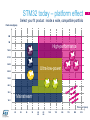
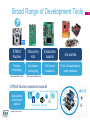
STM32L4 MCU series Excellence in ultra-low-power with performance Embedded Systems Conference 2015 Agenda Presentation 1:00-5:00 • System check for pre-installed tools • STM32L4 Family Overview • Hands On Session: Out-of-the-box demos • STM32L4 Low Power details • Hands On Lab#1: Getting Started with CubeMX and STM32L4 • STM32L4 Peripheral details • Hands On Lab#2: printf() debugging via onboard ST-LINK • Hands-On Lab#3: 3-axis MEMS Gyro communications • Hands-On Lab#4: Autonomous peripherals: ADC/TIM/DMA app 2 Systems Check • Please use this checklist to verify whether you have completed the steps to download and install all necessary components for this hands-on seminar. • I have a compatible laptop. • A Windows® Laptop (Windows 7 or Windows 8) • MacBook running Windows (Parallels, VM Fusion, etc) • Note: Administrator rights are needed for software and driver installation. • I have downloaded the Seminar Installer from the emailed Dropbox link and installed it (this would have installed latest Java, STM32CubeMX, STM32CubeL4 HAL, and extracted seminar files to C:\STM32CubeSeminar\) • I have installed the STM32 ST-LINK Utility by running its installer (this would also have installed the ST-LINK/V2 Windows device drivers). • I have downloaded and installed IAR EWARM v7.40 • Important please make sure you activate the 30-day time-limited evaluation license (or you already have a full license). The size-limited evaluation license will not be suitable for the seminar classes. • The workshop exercises require a ‘Discovery kit with STM32L476VG MCU’ (32L476GDISCOVERY) See the Distributor Availability listed at the bottom of the linked page. 3 STM32 today – platform effect Select your fit product inside a wide, compatible portfolio Flash size (bytes) 2M 1M High-performance 768 K 512 K 384 K Ultra-low-power 256 K 128 K 64 K 32 K Mainstream 16 K Pin count (pins) 20 28 36 32 48 49 63 64 100 132 144 176 208 216 4 Broadest 32-bit MCU product portfolio CoreMark 75 93 273 106 177 245 398 608 1000 5 Broad Range of Development Tools STM32 Nucleo Discovery kits Evaluation boards 3rd parties Flexible prototyping Key feature prototyping Full feature evaluation From full evaluation to open hardware www.st.com/stm32nucleo www.st.com/stm32discovery STM32 Nucleo expansion boards Specialized functionality add-on www.st.com/x-nucleo Connectivity, Sensors… 6 NEW STM32 Nucleo features Flexible board power supply Through USB or external source Integrated ST-Link/V2.1 Mass storage device flash programming Virtual COM port for communications 2 push buttons, 2 color LEDs Arduino™ extension connectors Easy access for add-ons One STM32 MCU flavor with 64 pins Morpho extension headers direct access to all MCU I/Os 7 Comprehensive choice of IDEs STM32CubeMX Partners IDEs STMStudio Generate Code Compile & Debug Monitor Free IDE 8 STM32Cube Supporting all STM32 MCUs • Generate your configuration code with the STM32Cube and you can focus on your added-value software ! • 4 configuration wizards: pinout, clock, peripherals & middleware, power consumption • Portable Hardware Abstraction layer, from series to others • Middleware with RTOS, USB, TCP/IP, File System, Graphics , Touch sensing… www.st.com/stm32cube 9 Comprehensive choice of STM32 free IDEs tools System Workbench CoIDE MDK-ARM Q2’2015 Q2’2015 Free licenses for all STM32 microcontrollers Free licenses for STM32F0 & STM32L0 Free access to all STM32Nucleo users New ST MCU Finder Application • Quickly find the right ST MCU • Easy access to technical materials • Latest news from ST MCU world www.st.com/stmcufinder 11 Birth of the STM32 L4 High-performance ARM Cortex-M4 FPU, DSP Advanced analog, New digital peripheral set Ultra-low-power • STM32L4 is a perfect fit in terms of ultra-low power, performances, memory size, and peripherals at a cost effective price. • Convergence between High performance and Ultra-low power series 12 Key messages of STM32 L4 series 1 ULP leader and performance booster ST has built a new architecture delivering best-in-class, ultra-low-power (ULP) figures thanks to its high flexibility. In addition the performance of the STM32L4 far exceeds the competition in the ultra-low-power world. It delivers 100 DMIPS based on its ARM Cortex-M4 core with FPU and ST ART Accelerator™ at 80 MHz. 2 Innovation Covering a large range of applications the STM32L4 features many architectural innovations and new smart embedded peripherals. 3 Integration and safety 1 MB of Flash and 128 KB of SRAM with safety and security features, smart and numerous peripherals, advanced and low power analog circuits in packages as small as 3.8 x 4.4 mm. 4 Great Investment This new STM32 member benefits from the pin-to-pin compatibility of the STM32 family and the STM32 Ecosystem. 13 EEMBC ULPBench STM32L4 gets 150.2 EEMBC ULPMark-CP, proving excellence in ULP ULMark-CP Ultra-low-power CoreMark Performance The higher, the better! 180 300 160 156 150 140 120 160 250 200 119 100 150 80 60 100 40 50 20 0 0 MCU-R MCU-M MCU-A MCU-T STM32L4 1 MCU-T MCU-A ULP leader and performance booster 3 Ultra-Low-Power and Flexibility 15 FlexPowerControl STM32L4 is based on a new platform optimized to reduce power consumption and increase flexibility Down to 30 nA for I/O wake-up with additional Shutdown mode External level shifter no longer needed Separate VDD supplies (down to 1.08 V) Down to 360 nA keeping 32 Kbytes of SRAM active in Standby mode 4 nA VBAT mode with charging capability Automatic switch to maintain power for RTC and backup registers STM32L4 Wake up MCU with any peripheral (Communication I/Fs, analog circuits, timers…) I/O level kept in low power modes Optimization of system consumption RTC available for all power modes (from Active down to VBAT) USB capable with 32 kHz crystal oscillator (Dedicated crystal oscillator is no longer needed for USB function) Internal oscillator from 100 kHz to 48 MHz (+/-0.25% int. 1 clock accuracy over voltage/temperature with LSE) 1 ULP leader and performance booster Ultra-low-power modes 16 Best power consumption numbers with full flexibility Wake-up time VBAT 4 nA / 300 nA* 250 µs SHUTDOWN 14 µs STANDBY 14 µs STANDBY + 32 KB RAM 5 µs STOP 2 (full retention) 4 µs STOP 1 (full retention) 6 cycles Tamper: 3 I/Os, RTC Wake-up sources: reset pin, 5 I/Os, RTC 30 nA / 330 nA* SLEEP 130 nA / 430 nA* Wake-up sources: + BOR, IWDG 360 nA / 660 nA* Wake-up sources: + all I/Os, PVD, LCD, COMPs, I²C, LPUART, LPTIM 1.1 µA / 1.4 µA* 7.3 µA / 7.6 µA* 35 µA / MHz RUN at 24 MHz Wake-up sources: + all I²C, UART Wake-up sources: any interrupt or event 100 µA / MHz RUN at 80 MHz 112 µA / MHz 1 Note : * without RTC / with RTC 1 ULP leader and performance booster Efficient run and fast wake-up Ready for Launch Control ? From 0 to 48 MHz in less than 5 µs • Thanks to our internal oscillator (MSI) used at start-up (programmable from 100 kHz to 48 MHz) Run 48 MHz < 5 µs! • PLL wake-up time < 15 µs (needed to reach fMAX) STOP mode 1 ULP leader and performance booster Run 80 MHz 17 Providing more performance Do not compromise on performance with STM32L4 CoreMark score Execution performance from Flash 273 • Up to 80 MHz/ 100 DMIPS with ART Accelerator™ Linear performance thanks to ST ART AcceleratorTM • Up to 273 CoreMark Result • ARM Cortex-M4 with DSP instructions and floating-point unit (FPU) • Optimized DMA (14 channels) Competitors: impact of wait states • SPI up to 40 Mbit/s, USART 10 Mbit/s CPU frequency 80 MHz 1 ULP leader and performance booster 7 High integration 13 High integration with high memory size in small packages Parallel Interface Connectivity Display Cortex-M4 80 MHz FPU MPU ETM LCD driver 8 x 40 DMA Timers ART Accelerator™ FSMC 8-/16-bit (TFT-LCD, SRAM, NOR, NAND) 17 timers including: 2 x 16-bit advanced motor control timers 2 x ULP timers 7 x 16-bit-timers 2 x 32-bit timers Up to 1-Mbyte Flash with ECC Dual Bank I/Os 128-Kbyte RAM Up to 114 I/Os Touch-sensing controller USB OTG, 1x SD/SDIO/MMC, 3 x SPI, 3 x I²C, 1x CAN, 1 x Quad SPI, 5 x USART + 1 x ULP UART, 1Digital x SWP Package size down to 4.4 x 3.8 mm AES (256-bit), TRNG, 2 x SAI, DFSDM (8 channels) Analog 3 x 16-bit ADC, 2 x DAC, 2 x comparators, 2 x op amps 1 x temperature sensor 3 Integration and safety Safety and security Integrated safety and security features ULP with performance SECURITY SAFETY • Brown-out Reset in all modes • Clock Security System • SRAM parity check • Backup byte registers • Supply monitoring • Flash with ECC with status register (address) • Dual watchdog • Anti-tamper detection • Memory Protection Unit (MPU) • Read and Write Protection • Unique ID • AES-256 Encryption • JTAG fuse • True Random Number Generator • Software IP Protection 3 Integration and safety 14 STM32L4: continuity in STM32 portfolio 9 product series / 32 product lines STM32L4 benefits from pin-to-pin compatibility across the family 2 High-performance 398 CoreMark 120 MHz 150 DMIPS 106 CoreMark 48 MHz 38 DMIPS Ultra-low-power 93 CoreMark 32 MHz 33 DMIPS Cortex-M0 Cortex-M0+ Cortex-M3 1 000 CoreMark 200 MHz 428 DMIPS 6 (*) from CCM-SRAM 1 3 75 CoreMark 32 MHz 26 DMIPS 1 245 CoreMark* 72 MHz 90 DMIPS 177 CoreMark 72 MHz 61 DMIPS 3 608 CoreMark 180 MHz 225 DMIPS 5 4 Mainstream 7 273 CoreMark 80 MHz 100 DMIPS Cortex-M4 Cortex-M7 number of lines 4 Great investment 21 STM32L ULP offer STM32L4 completes the ultra-low-power family Cost-smart ULP Champion Broad Range Foundation ULP with performance Cortex-M0+ @ 32 MHz Operating range: 1.65 to 3.6V 8/16-bit applications Numerous pin counts Cortex-M3 @ 32 MHz Operating range: 1.65 to 3.6V Wide choice of memory sizes Cortex-M4 w/ FPU @ 80 MHz Operating range: 1.71 to 3.6V Advanced Peripheral Performance 3 product lines, Cost-effective, Smaller packages USB, LCD, Analog 16 to 192 Kbytes of Flash Up to 20 Kbytes of SRAM 3 product lines, USB, LCD, AES, Rich Analog True EEPROM, Dual bank Flash (RWW) 32 to 512 Kbytes of Flash Up to 80 Kbytes of SRAM 3 product lines, ADC 5 Msps, PGA, Compar., DAC, op amp, USB OTG, LCD, AES 256 Kbytes to 1 Mbyte of Flash Up to 128 Kbytes of SRAM 4 Great investment 16 STM32L, a complete offer STM32L4 completes the ultra-low-power family 100 DMIPS 273 CoreMark Performance More performance More memory and pin counts More packages Flash size (bytes) WLCSP 1M QFN 512 K 33 DMIPS 93 CoreMark 26 DMIPS 75 CoreMark 384 K 256 K 192 K 128 K BGA 64 K 32 K 16 K 8K MHz 32 32 80 20 28 36 32 48 49 63 100 132 144 64 4 Pins LQFP Great investment 17 Cortex®-M4 (DSP + FPU) – 80 MHz STM32L4 series • • • • • • • 8-ch / ART Accelerator™ 2 x 4x USART, SPI, I²C Product Flash RAM Memory 2x Op Sigma Quad SPI line (KB) (KB) I/F Comp amps Delta 16 and 32-bit timers Interface SAI + audio PLL SWP 512 STM32L471 SDIO 1x CAN to 128 Access FSMC 1024 • • 2x 12-bit DAC Temperature sensor STM32L475 USB OTG • Low voltage 1.71 to 3.6 V VBAT Mode Unique ID Capacitive Touch sensing • • • Legend: 16- bit Segment USB2.0 AES ADC LCD OTG FS 128/256-bit (5 Msps) Driver 3 256 to 1024 128 SDIO FSMC 3 STM32L476 256 USB OTG & to LCD 1024 128 SDIO FSMC 3 Up to 8x40 STM32L486 USB OTG & 1024 LCD & AES 128 SDIO FSMC 3 Up to 8x40 Available in Q4/2015 4 Great investment 18 STM32L4 portfolio Flash size (bytes) STM32L486RG 1M STM32L486JG STM32L486VG STM32L486QG STM32L486ZG 5 STM32L476RG STM32L476JG STM32L476VG STM32L476QG STM32L476ZG 512 K STM32L476RE STM32L476JE STM32L476VE STM32L476QE STM32L476ZE 256 K STM32L476RC UFBGA132 (7x7x0.6 mm) LQFP144 (20x20x1.4 mm) STM32L476VC Pin count LQFP64 WLCSP72 LQFP100 (10x10x1.4 mm) (4.4x3.8x0.585 mm) (14x14x1.4 mm) Legend: With 128/256-bit AES Hardware Encryption Without 128/256-bit AES Hardware Encryption 4 Available in Q3/2015 Great investment 19 STM32L4 ecosystem HARDWARE TOOLS SOFTWARE TOOLS (Available in Q3/2015) STM32 Nucleo Discovery kit (Available in Q3/2015) Evaluation board STM32CubeMX featuring code generation and power consumption calculation 5 Flexible prototyping Key feature prototyping Full feature evaluation 4 Great investment 26 STM32L476 Discovery – HMI Integrated ST-Link/V2-1 (for programming and debugging) LCD 96 segments Motion Mems (9-axis) push buttons and joystick, 2 color LEDs Quad SPI NOR Flash 16 MB USB OTG connector 27 27 STM32L476 Discovery - Audio and connector 28 APC connector (for Apple connector) MFX to auto-measure power consumption Direct access to all MCU I/Os Audio Codec and 3.5 mm connector Microphone Mems 28 STM32L476 Discovery - back side 29 Flexible board power supply CR2032 battery or USB IDD current consumption Mode Description Run Run 24Mhz, voltage range 2, PLL off, RTC/LSE off, Flash ART on Sleep Sleep 24Mhz, voltage range 2, PLL off, RTC/LSE off, Flash ART on Low-power run Low Power Run 2Mhz, PLL off, RTC/LSE off, Flash ART on Low-power sleep Low Power Sleep 2Mhz, PLL off, RTC/LSE off, Flash ART on Stop 2 RTC/LSE off, Flash ART off Standby RTC/LSE off, Flash ART off, RAM retention off Shutdown RTC/LSE off, Flash ART off 30 Audio demonstrations • RECORD application • Uses MP34DT01 MEMS microphone (LED5 toggling during record) • 16-bit audio samples @ 48 kHz stored in N25Q128A13 QuadSPI Flash • LEFT key to exit • PLAYER application • Uses CS43L22 audio DAC and 3.5mm jack output • Audio playback either from internal or QuadSPI Flash after a RECORD. Sub-menus : • “FLASH” : Audio playback of any WAV binary file loaded @ 0x08020000 • “QSPI” : Audio playback from QuadSPI Flash (following RECORD application) • Options : • SEL key to pause/resume playback • UP/DOWN keys to control volume • Audio is played back in loops until LEFT key is pressed 31 Compass and sound meter demonstrations • COMPASS application • Uses LSM303C eCompass MEMS device • 3D accelerometer and 3D magnetometer • Sub-Menu • • “CALIB”: rotate board (360° on all axis's) after scrolling message invitation “RUN”: displays angle in degrees • LEFT key to exit • SOUND meter application • Uses MP34DT01 audio sensor to measure ambient noise • Displays measurement value in dB on LCD screen • LEFT key to exit 32 Guitar tuner demonstration • Select guitar string • • • • • • “STR1”: “E” (low E, thickest string, closest to the ceiling) “STR2”: “A “STR3”: “D” “STR4”: “G” “STR5”: “B” “STR6”: “e” (high E, thinnest string, closest to the floor) • RIGHT/SEL to start recording • Ouputs : • • • • • “ ++ “ when string needs to be strained “ + “ when string needs to be slightly strained (close to correct tune) “ OK “ when string correctly tuned “ - “ when string needs to be slightly loosen (close to correct tune) “ -- ” when string needs to be loosen • LEFT key to exit 33 L476-Discovery Demonstration Source Code The “IDD Measure” app uses the “MFX” onboard STM32L151 as a non-intrusive auto-ranging current measurement probe. The target L4 will enter a low power state, the MFX will measure the current, wake the L4 up and report the measurement back over I2C. The project is in the CubeL4 library, Discovery Demonstrations folder: ..\STM32Cube_FW_L4_V0.4.0\Projects\STM32L476GDiscovery\Demonstrations\EWARM OR C:\Users\xxxx\STM32Cube\Repository\STM32Cube_FW_L4_V0.4.0\P rojects\STM32L476G-Discovery\Demonstrations\EWARM Open the IAR Project.eww workspace. • • • • Build/Program the L4 Discovery Board. Exit the debugger. RESET and run the Demo. Scroll to the Idd Measure app. Select different low power modes, wait for wakeup, and note the current consumption. STM32L151 Multi-Function Expander “MFX” 34 34 References • Refer to www.st.com/stm32l4-discovery • Ordering information • Getting Started Manual, User’s Manual and Application notes • Board Schematics • Application development environments support • Demonstration firmware sources • Video available on YouTube and st.com • “Getting started with STM32L476 discovery kit for ultra-low-power & performance applications” 35 Hands-On Lab #1: LED Blinky in Five Easy Steps! Run STM32CubeMX 37 Step 1: Create New Project • Create New Project • Select STM32L476VGT6 • LQFP100, 1024KB Flash • Click “OK” 38 Step 2: Pin Configuration • In this example we are going to use the LED’s present on the STM32L476 Discovery board. • Left-click PB2 & PE8 and set to GPIO_Output mode 39 Step 3: Generate Source Code • Open Project > Settings (Alt + P) • Set the project name (Lab1) and the project location (C:\STM32L4Seminar\Labs) • Set the IDE Toolchain to EWARM • Click OK • Generate Code (Ctrl + Shift + G) • Click Open Project 40 Step 4: Toggle The LED • The IAR EWARM IDE should now be open. • Expand the file tree and open the main.c file • Add the following code inside the while(1) loop • Line 85 in “main.c” • Add within “USER CODE BEGIN WHILE” / “USER CODE END WHILE” section (this will preserve your code after regeneration) HAL_GPIO_TogglePin(GPIOB, GPIO_PIN_2); HAL_Delay(100); HAL_GPIO_TogglePin(GPIOE, GPIO_PIN_8); HAL_Delay(100); 41 Step 5: Build the Project • Click “F7” or the “Make” button or use menu Project > Make. • Click the “Download and Debug” Green Arrow button (CTRL + D) • Click the “Go” button (F5) • Enjoy the flashing LED’s! 42 STM32CubeTM Introduction • STM32CubeTM includes: • A configuration tool, STM32CubeMX generating initialization code from user choices • Firmware offering, delivered per series (like STM32CubeF4) with: • An STM32 Abstraction Layer embedded software: STM32Cube HAL • A consistent set of Middleware: RTOS, USB, TCP/IP, Graphics, … STM32CubeMX STM32CubeL0 STM32CubeF4 STM32CubeL1 STM32CubeF0 STM32CubeF2 STM32CubeF1 STM32CubeF3 43 44 STM32CubeMX Pinout Wizard Peripherals & Middleware Wizard Power Consumption Wizard Clock Tree wizard Power consumption calculator • Power step definitions • Battery selection • Creation of consumption graph • Display of • Average consumption • Average DMIPS • Battery lifetime 45 STM32Cube Firmware Components Evaluation boards Discovery boards Nucleo boards Board Demonstrations Middleware level Applications Networking LwIP TCP/IP & Polar SSL Utilities USB Host & Device Graphics STemWin File system FATFS RTOS FreeRTOS Middleware HAL level Examples HAL Hardware Abstraction Layer API CMSIS Boards Support Packages Drivers STM32F401 Fx/Lx Family STM32F405/7 STM32F429 STM32F439 46 STM32L476 block diagram 47 Cortex-M processors binary compatible 48 ARM Cortex M4 Core 49 FPU Single precision Ease of use Better code efficiency Faster time to market Eliminate scaling and saturation Easier support for meta-language tools What is Cortex-M4? MCU Ease of use of C programming Interrupt handling Ultra-low power DSP Cortex-M4 Harvard architecture Single-cycle MAC Barrel shifter STM32L4 Bus matrix 50 DMA1 DMA2 Accel. S-bus D-bus I-bus Cortex M4 with FPU Flash 1 MB SRAM1 96 KB SRAM2 32 KB AHB1 Periph. AHB2 Periph. QUADSPI FMC Note: QuadSPI, FMC and SRAM1 I-bus & D-bus interfaces when remapped to 0x0000 0000 only APB1 Periph. APB2 Periph. Memory Mapping 51 0xFFFF FFFF • Reserved FLASH : up to 1 Mbytes, dual bank • 0xE010 0000 Cortex-M4 internal peripherals 0xE000 0000 • 0x1FFF FFFF Reserved Option Bytes FMC & QUADSPI registers 0xA000 0000 QUADSPI bank 0x1FFF C000 System Memory 0x1FFF 0000 Reserved SRAM2 0x1000 8000 • Reserved 0x0810 0000 0x0800 0000 Reserved 0x0010 0000 0x2000 0000 CODE 0x0000 0000 SRAM1 : 96 KBytes @2000 0000 SRAM2 : 32 KBytes @1000 0000 : Access through D-code and I-code Flash 0x4000 0000 SRAM1 FB_MODE = 1 in SYSCFG_MEMRMP 0x6000 0000 Peripherals Bank 2 @ 0x0808 0000 SRAM: Up to 128 Kbytes SRAM split in 2 parts : • • 0x1000 0000 0x9000 0000 FMC banks Bank 1 @ 0x0800 0000 Bank 2 @ 0x0800 0000 Bank 1 @ 0x0808 0000 0x1FFF C008 Reserved 0xB000 0000 FB_MODE = 0 in SYSCFG_MEMRMP: Memory type depending on boot configuration 0x0000 0000 • Physical remap at 0x0000 0000 selected by MEM_MODE in SYSCFG_MEMRMP: • Flash Bank 1 or Bank 2 (see FB_MODE) • System flash (bootloader) • FMC bank 1 • SRAM1 • QUADSPI Boot modes Boot mode selection BOOT1 BOOT0 (opposite of nBOOT1 option bit) (pin) x Boot mode Aliasing 0 User Flash Main Flash memory is selected as boot space 1 1 System memory System memory is selected as boot space 0 1 SRAM1 Embedded SRAM1 is selected as boot space • Flash Bank1 boot: Option Bit BFB2 = 0 • Flash Bank2 boot: Option Bit BFB2 = 1 • Bootloader supports: USART1/2/3, I2C1/2/3, SPI1/2/3, USB DFU 11/08/2015 52 32KB SRAM2 features • Access through D-code and I-code: 53 Code execution max performance without remap • HW parity check : 4 bit per word • Enabled with SRAM2_PE in user options bytes • NMI / Timer Break on parity check error • Optional retention in Standby mode • Write protection with 1 Kbyte granularity • Read protection with RDP : Erased when RDP changed from Level 1 to Level 0 • Software reset and optional Hardware reset when system reset • Erased when setting SRAM2ER in SYSCFG_SCSR SRAM2 control and status register • Erased with system reset with SRAM2_RST in user option bytes 11/08/2015 Flash organization • Two 512KB User Flash banks: • Each bank is 256 pages of 2KB • Information block: • System memory boot loader • 1 KB (128 double word) OTP for user data • Option bytes for user configuration Flash area Bank 1 Flash memory address 0x0800 0000 – 0x0800 07FF Size 2K … Main memory Bank 2 Page 0 … 0x0807 F800 – 0x0807 FFFF 2K Page 255 0x0808 0000 – 0x0808 07FF 2K Page 256 … Information block Name … 0x080F F800 – 0x080F FFFF 2K Page 511 Bank 1 0x1FFF 0000 – 0x1FFF 6FFF 28K Bank 2 0x1FFF 8000 – 0x1FFF EFFF 28K System memory Bank 1 0x1FFF 7000 – 0x1FFF 73FF 1K OTP area Bank 1 0x1FFF 7800 – 0x1FFF 780F 16 Option bytes Bank 2 0x1FFF F800 – 0x1FFF F80F 16 Presentation Title 11/08/2015 54 Program / Erase • ECC (Error Code Correction) : 8-bit for 64-bit word • Single error correction: • Failure address and bank saved in FLASH_ECCR register, optional interrupt • Double error detection : NMI! • Programming granularity is 64-bit • Page granularity for erase is 2 Kbytes Parameter Typ 64-bit programming time 82 µs Page (2 KB) erase time 22 ms One row (32 double-word) programming time Normal : 2.6 ms Fast : 1.9 ms One page (2 KB) programming time Normal : 20.9 ms Fast : 15.3 ms One bank (512 KB) programming time Normal : 5.35 s Fast : 3.9 s Mass erase time (1 or 2 banks) 22 ms 55 Performances Mode STM32L15x STM32L4x CPU CortexM3 CortexM4 + FPU Flash I/F Prefetch ART Frequency 32MHz 80MHz ~35 DMIPS ~100 DMIPS (no loss) Performance DMIPS STM32L4 STM32L15x MHz 56 ART overview • Instruction cache = 32 lines of 4x64 bits (1KB) • Data cache = 8 lines of 4x64 bits (256 B) • Best tradeoff between cache size, Power and Dhrystone/CM performances 64 64 64 64 ART I Cache 8x128 32x4x64 CM4 core I Current buffer (64) AHB 32 I Prefetch buffer (64) FLASH FLASH Memory Memory 128kx64 128kx64 57 Flash protections Flexible Protections configurable with option bytes : • Readout protection (RDP) • Forbids access to Flash/SRAM2/Backup registers by: • Debug interface (JTAG/SWD) • Boot from SRAM1 • Bootloader • Proprietary Code Protection (PCROP) with 64-bit granularity • Used to protect specific code area from any read or write access • The code can only be executed. • Write Protection (WRP) with 2-KByte granularity • Used to protect specific code area from unwanted write/erase 58 Readout Protections • Readout protection Level 0 : No read protection • All operations are possible in all boot configurations. • Readout protection Level 1 • User mode: Code executing in user mode can access main Flash memory, option bytes, RTC backup registers and SRAM2 with all operations. • Debug, boot RAM and boot loader modes: The main Flash memory, backup registers and SRAM2 are totally inaccessible in these modes, a simple read access generates a bus error and a Hard Fault interrupt. • Un-protection, Level 1 to Level 0: • Flash memory is mass-erased, RTC backup registers and SRAM2 are cleared • If Option bit PCROP_RDP is set, the PCROP-protected area is not erased • Readout protection Level 2 (No debug) • • • • All protections provided by Level 1 are active. RAM boot, System memory boot and all debug features are disabled Option bytes can no longer be changed in user mode. Un-protection is not possible. It is an irreversible operation 59 Proprietary Code (PCROP) / Write Protections • When enabled, PCROP area is protected against all D-code bus accesses • The PCROP regions are execute-only • 1 area per bank, 64-bit granularity. • PCROP area can be increased but never decreased • Only way to deactivate PCROP is to change RDP from Level 1 to Level 0 • Option bit PCROP_RDP • When DISABLED: PCROP content is erased when RDP is changed from Level 1 to Level 0. PCROP_RDP is locked in this state. • When ENABLED: PCROP content is preserved when RDP is changed from Level 1 to Level 0. • Flash Write Protection: • Write-protected area is protected against erasing and programming. • 2 areas per bank, 2-KByte granularity. 60 STM32 Firewall (FW) 61 • The FIREWALL is made to protect parts of code/data (volatile and non volatile) from access from the rest of the code executed outside of the protected area. Code Segment (NVM Code) 31 24 23 8 7 1 8 7 1 Start Address 31 22 21 FW_CSSA Length Cortex-M4 GP-DMA FW_CSL Protection : Code fetch Bus Matrix Non-Volatile Data Segment (NVM Data) 31 8 7 24 23 1 Start Address SRAM1 AHB/APB 31 FLASH FW_NVDSSA 8 7 22 21 1 Length Protection : Data NVM code NVM data Volatile Data FW_NVDSL FIREWALL Volatile Data Segment (SRAM1 Data) Reset event 31 17 16 8 7 1 8 7 1 Start Address 31 3 Segments may be protected by the Firewall 22 21 Length FW_VDSSA FW_VDSL Protection: - Code fetch if SRAM1 is executable (not shared) - Data 1 31 VDE VDS FPA FW_CR FPA : Pre-alarm bit to control the exit point of the protected code VDS : SRAM1 protected segment is sharable with non protected code VDE : SRAM1 is executable into the protected volatile data segment Clock Tree 62 Clocks: MSI (Multi-Speed Internal) • MSI = clock at startup from Reset, Standby or Shutdown modes. • 12 Programmable frequency ranges: 100 kHz, 200 kHz, 400 kHz, 800 kHz, 1 MHz, 2 MHz, 4 MHz (reset value), 8 MHz, 16 MHz, 24 MHz, 32 MHz, 48 MHz. • After Standby: Frequency selected from 1, 2, 4 or 8 MHz with MSISRANGE in RCC_CSR register. • Normal mode and PLL-mode (=auto-calibration with LSE) PLL-mode : allows USB FS device functionality (0.25% accuracy) • Factory and user trimmed 63 Clocks: HSI(High-Speed Internal) • HSI 16MHz, factory and user trimmed • Selectable as wakeup clock from STOP1 / STOP2 • Can be automatically woken up when exiting Stop modes • Can be used as I2C/USART/LPUART source upon wakeup 64 HSI vs. MSI (design spec) MSI Normal mode HSI PLL-mode Over temperature: ±6% Accuracy (max) Over voltage: From 100 to 800 kHz : ±1% From 1 to 8 MHz : ±2% From 16 to 48 MHz : ±4% Better than 0.25% TBD 100 kHz : 0.5 µA 800 kHz : 2µA Consumption (typ) 1 MHz : 5µA 130 µA 8 MHz : 20 µA 16 MHz : 60 µA 48 MHz : 160 µA Startup time (typ) 100 kHz : 10 µs 48 MHz : 2.5 µs 1.25 ms for 5% of final freq. 0.9 µs 65 Clocks: HSE(High-Speed External) • HSE 4-48MHz • External source (Bypass mode) up to 40 MHz • External Crystal/Ceramic resonator (4-48MHz) • Clock Security System (CSS) • Automatic detection of HSE failure with • NMI generation • Break input to TIM1/TIM8/TIM15/TIM16/TIM17 • Backup clock can be HSI or MSI 66 Clocks: PLL • 3 PLL’s • Each with 3 independent outputs • PLL input freq = 4-16 MHz • PLL input can be MSI/HSI or HSE 5,6,7,8 f(VCO clock) = (f(PLL clock input)/PLLM) × PLLN f(PLL_P) = f(VCO clock) / PLLP f(PLL_Q) = f(VCO clock) / PLLQ f(PLL_R) = f(VCO clock) / PLLR PLLM from 1 to 8 PLLN from 8 to 86 PLLP = 7 or 17 PLLQ = 2, 4, 6, 8 PLLR = 2, 4, 6, 8 PLLP from 2 to 31 in derivatives 67 Clocks: LSE (Low-Speed External) • LSE: programmable amplifier driving capability (4 modes) Mode Crystal (max) Consumption (typ) Ultra low power 50kOhm/6pF 200 nA Medium low driving 80kOhm/6pF 260 nA Medium high driving 50kOhm/12.5pF 410 nA High driving 80kOhm/12.5pF 540 nA • Available in all low-power modes + VBAT 68 Clocks: LSI (Low-Speed Internal) • LSI 32kHz Parameters STM32L15x STM32L4x Accuracy over parts 26..56KHz ~8% Accuracy over temperature -10% / +4% (0..85°C) Consumption (typ) 400nA 2% (-40 125°C) 110nA • Available in all low-power modes except Shutdown and VBAT 69 Power schemes (1/3) 70 2 OPAMP 2 COMP 3 ADC 2 DAC VREF buffer VDDA VREF+ VLCD LCD USB transceivers CPU SRAM1 SRAM2 Digital peripherals LCD booster Flash Reset block Temp. sensor 3 PLL, HSI, MSI VDD VDDIO1 I/O ring VDDIO2 VDDIO2 I/O ring VDDUSB VCORE Voltage Regulator Standby circuitry (wakeup, IWDG) Backup domain LSE, RTC, backup registers VBAT Peripheral Voltage Monitor • By default independent powers are electrically isolated and the features powered by them are not available • The power isolation must be removed by SW • Peripheral Voltage Monitor for VDDA, VDDUSB, VDDIO2: PVM Power supply PVM threshold EXTI line PVM1 VDDUSB VPVM1 = 1.2 V 35 PVM2 VDDIO2 VPVM2 = 0,9 V 36 PVM3 VDDA VPVM3 = 1.65 V 37 PVM4 VDDA VPVM4 = 2.2 V 38 71 Power supply Supervisor BOR complies with all VDD rise/fall time = no constraint on power supply shape VDD VBORx VBORx (rising edge) hysteresis VBORx (falling edge) tRSTTEMPO nReset 72 VCORE Voltage Regulator 73 • All high-speed digital IP is sourced by the VCORE power rail • Dynamic Voltage Scaling optimizes performance vs power • VCORE Voltage Range 1 = 1.2V (Up to 80MHz) • VCORE Voltage Range 2 = 1.0V (Up to 26MHz) • VCORE powered by main regulator (MR) or low-power regulator (LPR) • Main voltage regulator mode (MVR) for Run and Sleep modes. • Low-power regulator for LP run, LP sleep and STOP1/STOP2 modes. • Regulators OFF in Standby and Shutdown mode. • However LPR remains ON to preserve SRAM2 content in Shutdown mode, if required. 73 Dynamic voltage scaling in Run mode SYSCLK(MHz) 127µA/MHz @80MHz 80 4WS 64 3WS 48 2WS 32 1WS 1WS 111µA/MHz @26MHz 26 3WS 1WS 18 16 2WS 12 1WS 6 2 VCORE VDD 136µA/MHz @26MHz 0WS 0WS Low-power run VCORE = 1.1V Range 2 VCORE = 1.0V 0WS V Range 1 VCORE = 1.2V 1.71V .. 3.6V 74 Hands-On Lab #2 – printf() debugging Adding to the existing CubeMX project, we will add USART2 debug via the ST-LINK Virtual-COM port Set up additional GPIO / Clocks: PD5 – USART2, “VirtualCOM-TX” – Alt. Fn. Push/Pull PD6 – USART2, “VirtualCOM-RX” – Alt. Fn. Push/Pull PA0 – GPIO_EXTI0: External Interrupt on Rising Edge Input USART2 Clock = PCLK1 (80MHz) USART2 settings: Asynchronous Mode - 9600 N/8/1, No HW Flow control Tx/Rx, 16-sample oversampling No advanced features User Code HAL function calls required: See lab2_printf_debug.c in Lab2_Printf directory Also Need Terminal emulator (Hyperterm, etc) (Hyperterm.exe is included in Tools directory) USART2 is routed to the ST-LINK’s USART, and brought via the USB Virtual-COM port class (SB13/16 have been soldered) 75 75 GPIO Configuration additions • Expand the USART2 dialog, and select Asynchronous mode: • Use PD5 & PD6 for Tx / Rx pins: • These are the alternate mapping pins (PA2/3 are default) 76 Clock Configuration • We will run the STM32L4 at 80MHz for this lab • Click on the Clock Configuration tab • Set the PLL Source Mux to MSI • Set the System Clock Mux to PLLCLK • Use PLLM=/1, *N = x40, /R=/2 • AHB Prescaler = /1 • HCLK should equal 80MHz 77 USART2 Configuration • Click on the Configuration tab, and select USART2: • Parameter Settings tab: • 9600Bits/s • 8-bit word length • No parity bit • 1 Stop bit • Rx & Tx data • 16-clock oversampling • No advanced feature settings needed • No NVIC or DMA settings used 78 NVIC Configuration • Click on the Configuration tab, and select NVIC: • Enable EXTI line0 • Set Preemption Priority to 2 • Click ‘OK’ 79 Regenerate Source Code for Lab1 • Generate Code (Ctrl + Shift + G) • Open Project • Copy/Paste needed code bits for Hands-On Lab #2 into main.c: • C:\STM32L4Seminar\Labs\lab2_printf_debug.c • Open a terminal emulator, using USART2 settings, Virtual COM port xx • Rebuild • Program/Debug • Run! 80 Available Peripheral GPIO DMA FSMC QUADSPI BOR PVD, PVM LCD USB OTG USART LP UART I2C 1 / I2C 2 I2C 3 SPI CAN SDMMC SWPMI SAI DFSDM ADC DAC OPAMP COMP Temp Sensor Timers LPTIM 1 LPTIM 2 IWDG WWDG Systick Timer Touch Sens RNG AES CRC STM32L4 Power Mode Run mode Run Mode Range 1 Ex: execution from Flash Cortex M4 Main regulator (MR) Range 1 (up to 80MHZ) SRAM 1 (96KB) Flash (1MB) SRAM 2 (32KB) Range 2 (up to 26MHZ) Low Power regulator (LPR) Range 1 127uA/MHz at 80 MHz (10.2mA) Range 2 111uA/MHz at 26 MHz (2.9 mA) up to 2MHz Available Clock HSI HSE LSI LSE MSI Active cell Frozen cell Cell in power-down Available Periph and clock 81 Available Peripheral GPIO DMA DMA FSMC FSMC QUADSPI QUADSPI BOR PVD, PVM LCD USB OTG USART LP UART I2C 1 / I2C 2 I2C 3 SPI CAN SDMMC SWPMI SAI DFSDM ADC DAC OPAMP COMP Temp Sensor Timers LPTIM 1 LPTIM 2 IWDG WWDG Systick Timer Touch Sens RNG AES CRC STM32L4 Power Mode Low-power run mode Low-power run mode Ex: execution from Flash Cortex M4 Main regulator (MR) Range 1 (up to 80MHZ) SRAM 1 (96KB) Flash (1MB) SRAM 2 (32KB) Range 2 (up to 26MHZ) Low Power regulator (LPR) from Flash 136 µA/MHz at 2 MHz (272 µA) From SRAM1 121 µA/MHz at 2 MHz (242 µA) up to 2MHz Available Clock HSI HSE LSI LSE MSI Active cell Frozen cell Cell in power-down Available Periph and clock 82 Available Peripheral GPIO DMA DMA FSMC FSMC QUADSPI QUADSPI BOR PVD, PVM LCD USB OTG USART LP UART I2C 1 / I2C 2 I2C 3 SPI CAN SDMMC SWPMI SAI DFSDM ADC DAC OPAMP COMP Temp Sensor Timers LPTIM 1 LPTIM 2 IWDG WWDG Systick Timer Touch Sens RNG AES CRC STM32L4 Power Mode Sleep mode Sleep Mode Range 1 Ex: Flash ON, SRAMs ON (default) Zzz Cortex M4 Main regulator (MR) Range 1 (up to 80MHZ) SRAM 1 (96KB) Flash (1MB) SRAM 2 (32KB) Range 2 (up to 26MHZ) Low Power regulator (LPR) Range 1 37 µA/MHz at 80 MHz (2,96 mA) Range 2 35 µA/MHz at 26 MHz (0,92 mA) up to 2MHz Available Clock HSI HSE LSI LSE MSI Active cell Frozen cell Cell in power-down Available Periph and clock 83 Available Peripheral GPIO DMA DMA FSMC FSMC QUADSPI QUADSPI BOR PVD, PVM LCD USB OTG USART LP UART I2C 1 / I2C 2 I2C 3 SPI CAN SDMMC SWPMI SAI DFSDM ADC DAC OPAMP COMP Temp Sensor Timers LPTIM 1 LPTIM 2 IWDG WWDG Systick Timer Touch Sens RNG AES CRC STM32L4 Power Mode Low-power sleep mode Low-power sleep mode Ex: Flash OFF, SRAM1 OFF Zzz Cortex M4 Main regulator (MR) Range 1 (up to 80MHZ) SRAM 1 (96KB) Flash (1MB) SRAM 2 (32KB) Range 2 (up to 26MHZ) Low Power regulator (LPR) Flash ON, SRAMs OFF 48 µA/MHz at 2 MHz (96 µA) Flash OFF, SRAMs OFF 40,5 µA/MHz at 2 MHz (81 µA) up to 2MHz Available Clock HSI HSE LSI LSE MSI Active cell Frozen cell Cell in power-down Available Periph and clock 84 Available Peripheral GPIO DMA FSMC QSPI BOR PVD, PVM LCD USB OTG USART LP UART I2C 1 / I2C 2 I2C 3 SPI CAN SDMMC SWPMI SAI DFSDM ADC DAC OPAMP COMP Temp Sensor Timers LPTIM 1 LPTIM 2 IWDG WWDG Systick Timer Touch Sens RNG AES CRC I/Os kept, and configurable STM32L4 Power Mode 85 Stop 1 Mode Stop 1 w/ RTC on LSE quartz 7,9 µA @3.0V 7.6 µA @1.8V Wake-up event Zzz Cortex M4 Main regulator (MR) SRAM 1 (96KB) Flash (1MB) SRAM 2 (32KB) Available Clock HSI HSE LSI LSE MSI Low Power regulator (LPR) Backup domain Backup Register (32x32-bits) RTC NRST BOR PVD PVM RTC + Tamper LCD USB OTG USART LP UART I2C 1 / I2C 2 I2C 3 SWPMI COMP LPTIM 1 LPTIM 2 IWDG GPIOs 6us wake-up from Flash 4us wake-up from RAM Available Peripheral GPIO DMA FSMC QSPI BOR PVD, PVM LCD USB OTG USART LP UART I2C 1 / I2C 2 I2C 3 SPI CAN SDMMC SWPMI SAI DFSDM ADC DAC OPAMP COMP Temp Sensor Timers LPTIM 1 LPTIM 2 IWDG WWDG Systick Timer Touch Sens RNG AES CRC I/Os kept, and configurable STM32L4 Power Mode 86 Stop 1 Mode 7,5 µA @ 3.0V 7.3 µA @ 1.8V Stop 1 w/o RTC Wake-up event Zzz Cortex M4 Main regulator (MR) SRAM 1 (96KB) Flash (1MB) SRAM 2 (32KB) Available Clock HSI HSE LSI LSE MSI Low Power regulator (LPR) Backup domain Backup Register (32x32-bits) RTC NRST BOR PVD PVM RTC + Tamper LCD USB OTG USART LP UART I2C 1 / I2C 2 I2C 3 SWPMI COMP LPTIM 1 LPTIM 2 IWDG GPIOs 6us wake-up from Flash 4us wake-up from RAM Available Peripheral GPIO DMA FSMC QSPI BOR PVD, PVM LCD USB OTG USART LP UART I2C 1 / I2C 2 I2C 3 SPI CAN SDMMC SWPMI SAI DFSDM ADC DAC OPAMP COMP Temp Sensor Timers LPTIM 1 LPTIM 2 IWDG WWDG Systick Timer Touch Sens RNG AES CRC I/Os kept, and configurable STM32L4 Power Mode 87 Stop 2 Mode 1.66 µA @3.0V 1.43 µA @1.8V Stop 2 w/ RTC on LSE quartz Wake-up event Zzz Cortex M4 Main regulator (MR) SRAM 1 (96KB) Flash (1MB) SRAM 2 (32KB) Low Power regulator (LPR) NRST BOR PVD PVM RTC + Tamper LCD LP UART I2C 3 Available Clock HSI HSE LSI LSE MSI Backup domain Backup Register (32x32-bits) RTC COMP LPTIM 1 IWDG GPIOs 7us wake-up from Flash 5us wake-up from RAM Available Peripheral GPIO DMA FSMC QSPI BOR PVD, PVM LCD USB OTG USART LP UART I2C 1 / I2C 2 I2C 3 SPI CAN SDMMC SWPMI SAI DFSDM ADC DAC OPAMP COMP Temp Sensor Timers LPTIM 1 LPTIM 2 IWDG WWDG Systick Timer Touch Sens RNG AES CRC I/Os kept, and configurable STM32L4 Power Mode 88 Stop 2 Mode 1.25 µA @3.0V 1.19 µA @1.8V Stop 2 w/o RTC Wake-up event Zzz Cortex M4 Main regulator (MR) SRAM 1 (96KB) Flash (1MB) SRAM 2 (32KB) Low Power regulator (LPR) NRST BOR PVD PVM RTC + Tamper LCD LP UART I2C 3 Available Clock HSI HSE LSI LSE MSI Backup domain Backup Register (32x32-bits) RTC COMP LPTIM 1 IWDG GPIOs 7us wake-up from Flash 5us wake-up from RAM Available Peripheral GPIO DMA FSMC QSPI BOR PVD, PVM LCD USB OTG USART LP UART I2C 1 / I2C 2 I2C 3 SPI CAN SDMMC SWPMI SAI DFSDM ADC DAC OPAMP COMP Temp Sensor Timers LPTIM 1 LPTIM 2 IWDG WWDG Systick Timer Touch Sens RNG AES CRC I/Os can be configured w/ or w/o pull-up w/ or w/o pull-down STM32L4 Power Mode Standby Mode Standby w/ SRAM2 w/o RTC Zzz Cortex M4 405 nA @ 3.0V 363 nA @1.8V Main regulator (MR) SRAM 1 (96KB) Flash (1MB) SRAM 2 (32KB) Available Clock HSI HSE LSI LSE MSI Low Power regulator (LPR) Backup domain Wake-up event NRST BOR RTC + Tamper IWDG 5 WKUP pins Backup Register (32x32-bits) RTC 14 us wake-up 89 Available Peripheral GPIO DMA FSMC QSPI BOR PVD, PVM LCD USB OTG USART LP UART I2C 1 / I2C 2 I2C 3 SPI CAN SDMMC SWPMI SAI DFSDM ADC DAC OPAMP COMP Temp Sensor Timers LPTIM 1 LPTIM 2 IWDG WWDG Systick Timer Touch Sens RNG AES CRC I/Os can be configured w/ or w/o pull-up w/ or w/o pull-down STM32L4 Power Mode Standby Mode 674 nA @ 3.0V 433 nA@ 1.8V Standby w/ RTC on LSE quartz Zzz Cortex M4 Main regulator (MR) SRAM 1 (96KB) Flash (1MB) SRAM 2 (32KB) Available Clock HSI HSE LSI LSE MSI Low Power regulator (LPR) Backup domain Wake-up event NRST BOR RTC + Tamper IWDG 5 WKUP pins Backup Register (32x32-bits) RTC 14 us wake-up 90 Available Peripheral GPIO DMA FSMC QSPI BOR PVD, PVM LCD USB OTG USART LP UART I2C 1 / I2C 2 I2C 3 SPI CAN SDMMC SWPMI SAI DFSDM ADC DAC OPAMP COMP Temp Sensor Timers LPTIM 1 LPTIM 2 IWDG WWDG Systick Timer Touch Sens RNG AES CRC I/Os can be configured w/ or w/o pull-up w/ or w/o pull-down STM32L4 Power Mode Standby Mode 169 nA @ 3.0V 128 nA @ 1.8V Standby Zzz Cortex M4 Main regulator (MR) SRAM 1 (96KB) Flash (1MB) SRAM 2 (32KB) Available Clock HSI HSE LSI LSE MSI Low Power regulator (LPR) Backup domain Wake-up event NRST BOR RTC + Tamper IWDG 5 WKUP pins Backup Register (32x32-bits) RTC 14 us wake-up 91 Available Peripheral GPIO DMA FSMC QSPI BOR PVD, PVM LCD USB OTG USART LP UART I2C 1 / I2C 2 I2C 3 SPI CAN SDMMC SWPMI SAI DFSDM ADC DAC OPAMP COMP Temp Sensor Timers LPTIM 1 LPTIM 2 IWDG WWDG Systick Timer Touch Sens RNG AES CRC STM32L4 Power Mode I/Os can be configured w/ or w/o pull-up w/ or w/o pull-down But floating when exit from Shutdown Shutdown Mode Shutdown w/ RTC on LSE quartz 476 nA @ 3.0V 265 nA @ 1.8V Zzz Cortex M4 Main regulator (MR) SRAM 1 (96KB) Flash (1MB) SRAM 2 (32KB) Low Power regulator (LPR) Wake-up event NRST RTC + Tamper Available Clock HSI HSE LSI LSE MSI Backup domain 5 WKUP pins Backup Register (32x32-bits) RTC 250 us wake-up 92 Available Peripheral GPIO DMA FSMC QSPI BOR PVD, PVM LCD USB OTG USART LP UART I2C 1 / I2C 2 I2C 3 SPI CAN SDMMC SWPMI SAI DFSDM ADC DAC OPAMP COMP Temp Sensor Timers LPTIM 1 LPTIM 2 IWDG WWDG Systick Timer Touch Sens RNG AES CRC STM32L4 Power Mode I/Os can be configured w/ or w/o pull-up w/ or w/o pull-down But floating when exit from Shutdown Shutdown Mode 77 nA @ 3.0V 43 nA @ 1.8V Shutdown Zzz Cortex M4 Main regulator (MR) SRAM 1 (96KB) Flash (1MB) SRAM 2 (32KB) Low Power regulator (LPR) Wake-up event NRST RTC + Tamper Available Clock HSI HSE LSI LSE MSI Backup domain 5 WKUP pins Backup Register (32x32-bits) RTC 256 us wake-up 93 Low-power modes summary 94 Mode Regulator CPU Flash SRAM Clocks Yes ON(1) ON Any R1 Run R2 LPRun LPR Peripherals In Bold : wakeup source Consumption @ 1.8V All 127 µA/MHz All except OTG, SDMMC, RNG 111 µA/MHz 136 µA/MHz Yes ON(1) ON Any except PLL All except OTG, SDMMC, RNG No ON(1) ON(2) Any All Any IT or event R1 Sleep R2 LPSleep LPR No ON(1) ON(2) 7.3µA w/o RTC 7.6 µA w/RTC 4 µA RAM 6 µA Flash 1.2 µA w/o RTC 1.4 µA w/RTC 5 µA RAM 7 µA Flash OFF ON LSE/LSI Stop 2 LPR No OFF ON LSE/LSI Reset pin, all I/Os BOR,PVD,PVM,RTC,LCD,IWDG, COMPx,LPUART,I2C3,LPTIM1 LSE/LSI Reset pin, 5 WKUPx pins BOR, RTC, IWDG LSE Reset pin, 5 WKUPx pins RTC SRAM2 ON OFF Shutdown OFF + 235 nA DOWN DOWN OFF DOWN 6 cycles 35 µA/MHz 6 cycles No DOWN 37 µA/MHz 40 µA/MHz LPR OFF TBD All except OTG, SDMMC, RNG Any IT or event Stop 1 Standby N/A Any except PLL Reset pin, all I/Os BOR,PVD,PVM,RTC,LCD,IWDG, COMPx,DACx,OPAMPx,USARTx, LPUART,I2Cx,LPTIMx,OTG_FS, SWPMI LPR Wakeup time 1. Can be put in power-down and clock can be gated off 2. SRAM1 and SRAM2 can be gated off independently 128 nA w/o RTC 433 nA w/RTC 43 nA w/o RTC 265 nA w/RTC 14 µs 256 µs Low-power modes transitions LPSleep Sleep LPRun Shutdown Stop1 Run Standby Stop2 95 VBAT backup domain • VBAT charging : allows to charge a super-cap on VBAT through internal resistor when VDD is present • Battery charging is enabled by setting VBE bit in the PWR_CR4 register. • VBRS bit value in the PWR_CR4 register selects the resistor value Backup domain VDD VBAT 1.5 kΩ VDD domain VBE VBRS 5 kΩ Battery charging 96 Digital Filter for Sigma Delta Modulators 8 x parallel inputs with up to 24-bit data output resolution Smart peripherals Δ Metering 97 LCD Display VBAT with RTC for battery backup 240 nA in VBAT mode for RTC and 32x 32-bit backup registers 88×40 or 4×44 with step-up converter STM32L4 Anti Tamper pin 3 x tamper pins for battery domain TRNG & AES for Security 128-/256-bit AES key encryption hardware accelerator Electricity/Gas /Water Smart Meter SPI / UART/ SDIO for Wireless 3x SPIs (4x SPIs with the Quad SPI) 6x USARTs (ISO 7816, LIN, IrDA, modem) 1 x SDIO FSMC External memory interface for static memories supporting SRAM, PSRAM, NOR and NAND I/Os Up to 114 fast I/Os for buttons & relays 2 Innovation Smart Peripherals Industrial Sensors Motor Control : 2x 16-bit advanced motor-control timers 3x 12-bit ADCs: 5 MSPS, with up to 16-bit with hardware oversampling, 200 μA/MSPS LCD Display 8×40 or 4×44 with step-up converter STM32L4 CAN Bus High temperature (2.0B Active) from -40°C up to + 125°C TRNG & AES SPI / UART for Security 128/256-bit AES key encryption hardware accelerator 3x SPIs (4x SPIs with the Quad SPI) 6x USARTs (ISO 7816, LIN, IrDA, modem) FSMC I²C External memory interface for static memories supporting SRAM, PSRAM, NOR and NAND 3x I²C FM+(1 Mbit/s), SMBus/PMBus I/Os Up to 114 GPIOs 2 Innovation 98 Smart peripherals Fitness tracker application Digital Filter for Sigma Delta Modulators with PDM microphone input support 99 TFT Display STM32L4 Sensors FSMC Parallel interface to TFT SPI Up to 40 MHz speed I²C 3x I²C FM+ Batch Acquisition Mode (BAM) USB USB OTG 2.0 full-speed, LPM and BCD SPI / UART 3x SPIs Quad SPI 6x USARTs OPAMP 2x with built-in PGA DAC SAI 2x serial audio interfaces Low-power sample and hold SWP Single wire protocol master interface (SWPMI) ADC 3× 12-bit ADC 5 MSPS, 2 Innovation DFSDM Introduction • External SD modulators on market: • This is external standalone device: ADC converter on sigma delta principle • Analog input (usually differential) and digital output • Precision: ~16-bit resolution • Provides digital output as fast 1-bit data stream => serial interface • Up to 20MHz speed of serial data • Wide range of suppliers (ST, TI, Analog Devices) • STM32 interface: DFSDM = Digital Filter for Sigma Delta Modulators Implements complete post-processing from external SD modulators outputs: • Receiving of data streams from SD modulators (in various serial data formats) • Digital filtering of data stream (final 24-bit result) • Security/emergency functions 100 Memory buffer data (DMA/CPU transfer) 101 not in Orca Block diagram External SD modulator(s) Analog signal Decode, Filter, Average, Process • Up to 8 Serial transceivers: • Receive and decode raw serial bitstreams, providing data/clock to filter stage • 1-wire Manchester coded mode or SPI clock/data • Sincx filter performs input stream digital filtering: • Sinc1, Sinc2, Sinc3, Sinc4, Sinc5, FastSinc, No filter • Programmable Sincx oversampling ratio (1 to 1024 filter samples) • Output filter resolution is 31-bit max • Integrator stage performs data averaging from digital filter, 1-256 samples • Post processing: • Offset compensation • Programmable right bit shifting for data formatting • Additional functions • Min/Max extremes detection • Analog watchdog (to watch for final data boundaries overflow) • Break signal generation 102 MEMS microphone support (PDM) • Function • MEMS microphone provides pulse density modulated (PDM) data signal – like the SD modulator. • PDM microphone has stereo support (if two connected in parallel): • Rising clock = Left audio data, Falling clock = Right audio data • Implementation into DFSDM transceivers • Channels data (left vs. right) are separated inside: • Each DFSDM channel transceiver inputs can be redirected to next channel inputs • Configuration of those 2 channels differs only in active sampling edge • Clock signal provided by DFSDM_CKOUT – PDM microphones are slaves 103 MEMS microphone application - schematic DFSDM peripheral Channel 7 . . . DFSDM_DATIN3 DFSDM_DATIN2 MEMS microphone Right L data DFSDM_DATIN1 clock DFSDM_DATIN0 R data clock DFSDM_CKOUT Filter 2 Channel 3 Filter 1 R Filter 0 L Channel 2 Channel 1 - direct input falling edge sampling (R data) Channel 0 - redirected from next channel rising edge sampling (L data) internal clock Stereo microphone MEMS microphone Left Filter 3 104 Digital Filter for Sigma Delta Modulators Smart peripherals - DFSDM Δ Metering STM32L4 Electricity Meter 105 Digital Filter for Sigma Delta Modulators Smart peripherals - DFSDM Δ Metering STM32L4 Electricity Meter 106 Smart peripherals – Serial Audio Interface Fitness tracker application Serial Audio Interface supports a wide set of audio protocols thanks to its flexible architecture: • I2S Philips standards, (Inter-IC Sound) STM32L4 • I2S LSB or MSB-justified, (I2S variant) • SPDIF Output, (Sony/Philips Digital InterFace) • PCM, (Pulse Code Modulation) • TDM, (Time Division Multiplexing) • AC’97, (Audio Codec ’97 from Intel) SAI 2x serial audio interfaces 2 Innovation 107 SAI Features • SAI embeds two independent audio sub-blocks which can be: • Transmitter and/or receiver • Master or slave • Synchronous or asynchronous mode between the audio sub-blocks • Clock generator for each audio sub-block to target independent audio frequencies • 8-word integrated FIFOs for each audio sub-block, up to 16 slots available • Mute mode, Stereo/Mono and companding mode supporting µ-Law and A-Law. • Flexible serial interface: • Configurable LSB/MSB, data/slot sizes, sampling edges, # of bits, frame shape, etc.. • 2 DMA interfaces, 2 interrupts and a FIFO for each audio sub-block 108 SAI In The System STM32L476/486 SAI1 APB Interface 64 to 344 MHz SYNC OUT sync between both SAIs SAI1SEL 4 to 16 MHz Clk Gen PLL_P Clk Gen P HSE M ÷ [1:8] PLLSAI1 ÷ 7,17 APB Interface SAI2SEL PLLSAI2 ÷ 7,17 ÷N PLLSAI2_P SAI2 SAI2_CK_A P SAI2EXTCLK Clk Gen Sub-Block A Clk Gen Sub-Block B APB Interface SYNC IN SAI2_CK_B RCC FS1_A SCK1_A SD1_A MCLK1_A FS1_B SCK1_B SD1_B MCLK1_B P ÷N CMP APB Interface PLLSAI1_P IO Line Management HSI CMP MSI Sub-Block B SAI1_CK_B ÷N SYNC IN ÷ 7,17 SYNC OUT CMP PLL Sub-Block A IO Line Management SAI1_CK_A SAI1EXTCLK PLLSRC 109 FS2_A SCK2_A SD2_A MCLK2_A FS2_B SCK2_B SD2_B MCLK2_B Smart peripherals SAI: Discovery Board Implementation: STM32L4 SAI in I2S Philips mode 2 Innovation 110 Smart peripherals – I2C Fitness tracker application STM32L4 Sensors I²C • All known I2C limitations are corrected! • Flag management improvements (L0/F3-like) for easy use • Programmable filter on input pins (analog & digital filters) •Wake-up on address matches – STOP1 (I2C1/2/3), STOP2 (I2C3) •Fast mode Plus (up to 1Mbits/s) + 20mA •Dual clock domain allows high baudrates and low CPU clocks to save power 2 Innovation 111 Smart peripherals – USART/LPUART Fitness tracker application STM32L4 LPUART • Dual clock domain: • UART functionality and wake up from Stop mode (Stop 1 and Stop 2) • Baudrate programming independent of PCLK • Four clock sources: LSE (32.768KHz), HSI, PCLK, System Clock • Supports up to 9600 baud via 32.768KHz LSE! • To wakeup from STOP mode, clock source must be LSE or HSI • 3 Wakeup events: Address match, START bit detection or RXNE (receive buffer not empty) • KEY message: LPUART adds STOP2 wakeup, but is a subset of USART, however it is much lower power 2 Innovation 112 STM32L4 USART Implementation 113 • 3x USART’s, 2x UART’s and LPUART: USART features USART1/2/3 UART4/5 LPUART Hardware Flow Control YES YES YES Continous communication using DMA YES YES YES Multiprocessor communication YES YES YES Synchronous mode YES NO NO Smartcard mode YES NO NO Single wire half duplex mode YES YES YES IrDA YES YES NO LIN YES YES NO Dual clock / wake up from STOP1 YES YES YES Dual clock / wake up from STOP2 NO NO YES!! Receiver timeout YES YES NO Modbus Communication YES YES NO Autobaudrate detection YES YES NO RS-485 Driver enable YES YES YES Smart peripherals - SPI 114 STM32L4 SPI • Programmable frame from 4 to 16bit (bit granularity) • 32-bit FIFO to optimize bus bandwidth (performance & power consumption) • BUSY status bit IP fix • Up to 40 Mbits/s in master mode •I2S functionality no longer supported in SPI. Now in SAI peripheral 2 Innovation Hands-On Lab #3 – SPI communications to 3-axis Gyro Adding to the existing CubeMX project, we will add SPI communications to the L3GD20 MEMS gyroscope: Set up additional GPIO / Clocks: PD1 – SPI2 SCK – Alt. Fn. Push/Pull PD3 – SPI2 MISO – Alt. Fn. Push/Pull PD4 – SPI2 MOSI – Alt. Fn. Push/Pull PD7 – nCS – Output Push/Pull SPI2 settings: Full-Duplex Master Motorola, 8-bit MSB-first Prescaler /16 CPOL = Low, CPHA = 1-Edge No CRC Software NSS User Code HAL function calls required to be added to main.c: C:\STM32L4Seminar\Labs\lab3_spi_gyro.c Gyro (under LCD) data is routed to SPI2 115 115 Smart peripherals - QuadSPI 116 STM32L4 QuadSPI • Communication interface for single/dual/quad SPI flash memories 2 Innovation QuadSPI Overview • Three operating modes • Indirect : all the operations are performed through registers (classical SPI) • Status polling : periodical read of the flash status registers (interrrupt generation) • Memory mapped : External flash seen as internal for read operations – 256MB limit • SDR and DDR support • Integrated FIFO for reception and transmission • 8, 16, and 32-bit data accesses • DMA channel for indirect mode operations • Interrupt generation on FIFO threshold, timeout, operation complete, and access error QUADSPI Registers / Control Clock Management QSPI Flash CLK AHB BK1_IO0/SO BK1_IO1/SI FIFO Shift Register BK1_IO2 BK1_IO3 BK1_nCS CLK Q0/SI Q1/SO Q2/nWP Q3/nHOLD nCS 117 Frame format • Each of the 5 phases is fully configurable • Enabled or not • Length • Number of lanes • Exemple of Read configuration • Instruction on 1 lane • Address, Alternate & Data on 4 lanes • 2 dummy cycles Instruction Address Alt Dummy Data nCS SCLK IO0 7 6 5 4 3 2 1 0 4 0 4 0 4 0 4 0 4 0 4 0 IO1 5 1 5 1 5 1 5 1 5 1 5 1 IO2 6 2 6 2 6 2 6 2 6 2 6 2 IO3 7 3 7 3 7 3 7 3 7 3 7 3 A23-16 A15-8 A7-0 M7-0 IO switch from output to input Byte 1 Byte 2 118 Smart peripherals Sensor Hub scenario Sensors I²C STM32L4 I²C Wakeup from STOP Host App. Processor SPI / UART 3x SPI 6x USART Batch Acquisition Mode (BAM) Optimized mode for transferring data while the system is in low power mode Only the needed communication peripheral + 1 DMA + 1 SRAM (SRAM1 or SRAM2) are configured with clock enable in Sleep mode Flash is in power-down mode Enter either Sleep or Low-power sleep mode I2C clock can be at 16 MHz, allowing FM+ support 2 Innovation 119 Smart peripherals – USB OTG FS 2.0 120 • USB 2.0 / OTG 2.0 compliant • VDDUSB: Dedicated 3.3V supply input • 6 bidirectional endpoints STM32L4 • MSI in PLL mode (auto-trimmed with LSE) to reach 48MHz & < 0.25% accuracy • HSE not needed •Link power management (LPM) support • New power-save state, L1 (Sleep), with fast entry/exit compared to traditional L2 state (Suspend): 50uS vs 10mS •Battery charging detection (BCD) support • Detect and identify the port type (standard or charging) •Attach Detection Protocol (ADP) support USB USB OTG 2.0 full-speed, LPM and BCD • Allows an OTG device, embedded host or USB device to determine attachment status in the absence of bus power •Suspend/resume support • Wakeup from STOP 2 Innovation Analog Peripherals Smart peripherals 121 • OPAMP’s: • • • • Rail-to-rail inputs, 1mV offset after calibration Outputs: 500µA (sink/source), 100µA (low-power mode) 1MHz GBW (normal mode), 500kHz (low-power mode) 0.7V/µs slew rate (normal), 0.3V/µs (low-power Mode) STM32L4 • Comparators: • 2 Comparators • Window mode • Available in low-power modes • DAC’s: • • • • • 8/12-bit mode Lots of conversion triggers Programmable output buffer to drive more current Supply: VDDA = 1.8 V to 3.6 V NEW! Sample and hold low-power mode •ADC’s: • • • • • • • ADC1/ADC2 are tightly coupled, ADC3 is standalone Consumption linear vs. conversion rate : 200 µA / MSPS Dual-clock architecture Up to 5.3Ms/s with 12-bit resolution in single mode Single-ended or differential inputs Internal channels: Temp sensor, VREF, VBAT/3, DAC NEW! Hardware Oversampling OPAMP 2x with built-in PGA COMP 2x Low-power DAC 2x Low-power sample and hold ADC 3× 12-bit ADC 5 MSPS 2 Innovation DAC1 / DAC2 block diagram DAC Control Register TIM7_TRGO DMAENx TIM8_TRGO TENx MAMPx[3:0] SWTRIGx TIM6_TRGO WAVEx[1:0] TSELx[2:0] TIM2_TRGO TIM4_TRGO TIM5_TRGO Control Logic x Ext_IT_9 DMA Request x 12 bits Noise/triangle DHRx BOFF 12 bits DORx 12 bits VREF+ VDDA VSSA Digital to Analog Converter x DAC_OUTx 122 NEW! Sample & Hold feature • Maintains DAC output voltage when the MCU is in a low power mode, such as STOP1 mode • In Sample & Hold mode the DAC is able to hold its’ output voltage while all related analog and digital blocks are shut off • Up to 15x power savings in some configurations! Vout 123 How it works? • Sampling phase: During this phase, the “sample & hold” element is charged into the desired voltage. • Holding phase: During which the DAC’s output is tri-stated (High-Z) to maintain the “Sample & Hold” element’s stored electrical charge. • Refresh phase: Due to leakage coming from several sources, a refresh phase is essential to keep the output voltage at the desired value (+/- LSB) DAC (Sample & Hold mode) Cload Vout Vout 124 Voice recognition Demonstration 125 • STM32L4 with voice recognition algorithm controls an Android remote device thanks to Bluetooth Low Energy communication + Microphone Shield With Digitals MEMS (MP34DT01) + Nucleo STM32L4 + ST BlueNRG BLE RF Arduino Shield CR2032 Voice recognition function blocks Always on acquisition (PDM to PCM & signal conditioning) Always on BLE connection Low power sound detector Voice trigger detection 126 Low power audio DSP replacement Voice recognition example Always on acquisition (PDM to PCM & signal conditioning) < 410 µA Low power sound detector Voice trigger detection < 2.2 mA Sub-microwatt acquisition thanks to PDM to PCM HW processing with DFSDM and low power Batch Acquisition Mode (BAM) 6 Hardware/Software blocks PDM Input (1MHz) Digitals MEMS (MP34DT01) PDM LP Filter and Decimation Decimation by 64 Signal Conditioning Gain control HP filtering Filtering / Decimation / Gain control done by HW PCM Output Low Power Sound Detector (LPSD) @ 16MHz Voice Trigger Detection PCM Output (16kHz) @ 2MHz Indicator 128 BAM explained Voice recognition use case STM32L476 DMA DFSDM DFSDM 0111010100101001010101111 128 KB RAM Filtering / Decimation / Gain control done by HW with DFSDM Current consumption 0111011000010 0011010 Cortex-M4 ART 1024 KB FLASH Cortex-M4 Flash fetch BAM Cortex-M4 RAM fetch Cortex-M4 RAM fetch LPSD Quiet LPSD Detected BAM Algorithm Processing Voice trigger detection 7 Voice acquisition with DFSDM Zzz Zzz Cortex M4 Main regulator (MR) Zzz Range 1 (up to 80MHZ) Zzz Flash (1MB) SRAM 1 (96KB) SRAM 2 (32KB) DMA Digitals MEMS (MP34DT01) DFSDM 1MHz available Range 2 (up to 26MHZ) Low Power regulator (LPR) 0111011000010 ART CPU OFF, Flash OFF, 40 µA/MHz at 2MHz (81 uA) up to 2MHz MSI 2MHz available Acquisition : CPU OFF, ART OFF, Flash OFF, SRAM ON 130 Trigger detection Voice computation HSI ART Flash (1MB) SRAM 1 (96KB) SRAM 2 (32KB) Main regulator (MR) 0111011000010 011101100 16MHz available Cortex M4 Range 1 (up to 80MHZ) CPU ON, Flash ON, 114 µA/MHz at 16MHz (1.83 mA) Range 2 (up to 26MHZ) Low Power regulator (LPR) up to 2MHz Zzz DMA Digitals MEMS (MP34DT01) DFSDM 1MHz available MSI 2MHz available Computation : CPU ON, ART ON, Flash ON, SRAM ON 131 ADC Block Diagram 132 VREF+ VDDA ADEN/ADDIS VOPAMPx VTS VINN [18:0] VREF- SAR ADC Sample and hold 12bits 12bits Start AUTDLY oversampler VINP [18:0] Address/data bus ANALOG MUX ADC_IN[15:1] DMA Request ADCAL VREFINT VBAT Injected data register (4x16bits) Regular data register (16bits) Start & Stop 3 Analog watchdog ADSTP Control S/W trigger AREADY EOSMP EXTI0 EOS EOC OVR JEOS JQOVF AWDx EXTI1 . . . . . Analog Watchdog H/W trigger AREADYIE EOSMPIE EXTI15 EOCIE EOSIE OVRIE JEOSIE JQOVFIE AWDxIE High Threshold register (12bits) EXTSEL[3:0] bits Low Threshold register (12bits) J S/W trigger JEXTI0 JEXTSEL[3:0] bits AWD3_OUT JEXTI15 AWD2_OUT . . . . . AWD1_OUT JEXTI1 ADC interrupt to NVIC TIMERs ADC Clocks ADC1, ADC2 & ADC3 HCLK Reset & Clock controller AHB interface Analog ADC1 (master) /1 , /2 or /4 ADC123_CK /1 … /256 Analog ADC2 (slave) CKMODE[0:1] Analog ADC3 (single) 133 ADC Sampling Time (TSampling) • Three bits programmable sampling time channel by channel programmable: ADC 2.5 cycles 6.5 cycles 12.5 cycles ADCCLK 24.5 cycles 47.5 cycles Selection 2.5 cycles 6.5 cycles 12.5 cycles 24.5 cycles 47.5 cycles 92.5 cycles 247.5 cycles 640.5 cycles Sample Time • • • • • • • • 92.5 cycles 247.5 cycles 640.5 cycles SMPx[2:0] Note: The sampling time value depends on the type of channel (fast or slow), the resolution and output impedance of the external signal source to be converted 134 Total Conversion Time • Total conversion Time = TSampling + TConversion Resolution Resolution TConversion 12 bits 12.5 Cycles 10 bits 10.5 Cycles 8 bits 8.5 Cycles 6 bits 6.5 Cycles Total conversion Time (When FADC = 80MHz) 12 bits 12.5 + 2.5 = 15cycles 18.75 us 5.33 Msps 10 bits 10,5 + 2.5 = 13 cycles 16.25 us 6.15 Msps 8 bits 8.5 + 2.5 = 11 cycles 13.75 us 7.27 Msps 6 bits 6.5 + 2.5 = 9 cycles 11.25 us 8.89 Msps 135 Oversampler • Oversampler performs data pre-processing to offload the CPU. Handles up to 256 conversions and averages them • For : Averaging, Data rate reduction, SNR improvement, Basic filtering 12bit data ADC 20 bit register 0 to 8 bit right shift DATA SHIFTER, TRUNCATER Accumulation data register + 16 bit register ADCx_DR • Programmable oversampling ratio • x2, x4, x8, x16, x32, x64, x128, x256 • Programmable data shifting / truncating • Right shift 0 to 8 bits Example: Oversampling ratio x2 CH1(0) Trigger for oversampling channel CH1(1) CH1(0) EOC Trigger CH1(1) Sampling Conversion End of conversion for oversampling channel 136 ADC Analog Watchdogs • ADC Analog Watchdog 1 • 12-bit programmable analog watchdog low and high thresholds • Enabled on one or all converted channels • Interrupt generation on low or high thresholds detection • ADC Analog Watchdog 2&3 NEW! • Enabled on some selected channels by programming bits in AWDCHx[18:0], • Resolution Limited to 8 bits and only the 8 MSBs of the thresholds can be programmed ADC_IN0 ADC_IN1 . . . . . . ADC_IN18 AWD Analog Watchdog Low Threshold High Threshold Status Register 137 COMPARATORS 138 • 2 ultra-low power comparators: COMP1 / COMP2 • Wake-up from low-power modes thru EXTI (Sleep / STOP1 / STOP2) • Multiplexed inputs (GPIO, DAC’s, VREFINT) • Programmable hysteresis and speed-vs-consumption • Redirection of output to IO or timer inputs (e.g. TIM Break event) • Outputs with blanking source • Comparators can be combined in the window comparator COMP low power features Power consumption -vs- propagation delay can be adjusted: PWRMODE Max propagation delay Consumption (Typ) 00 80 ns 70 µA 01 or 10 1 µs 5 µA 11 12 µs 350 nA LP mode Feature / limitation Run, LPRun no limitation, state polling or interrupt thru EXTI Sleep, LPSleep wakeup capability thru EXTI Stop 1, Stop 2 wakeup capability thru EXTI Standby not available Shutdown not available 139 Smart peripherals 140 NOR NOR Signals TFT Display IRQ STM32L4 Config NAND AHB Shared Signals FMC Parallel interface to TFT SPI Up to 40 MHz speed • NOR Flash/PSRAM and NAND controllers • Differences from FSMC: • Continuous FMC clock generation for synchronous and asynchronous modes. • Performance enhancement • Removal of PCCard controller on new products. 2 Innovation FMC Bank memory mapping • For the FMC, the external memory is divided into 4 fixed size banks of 4x64 MB each: • Bank 1 can be used to address NOR Flash, OneNAND or PSRAM memory devices. • Banks 3 is used to address NAND Flash devices. • Bank 2 & 3 reserved Supported Memory Type 0x6000 0000 0x6FFF FFFF 0x7000 0000 0x7FFF FFFF 0x8000 0000 0x8FFF FFFF 0x9000 0000 0x9FFF FFFF Bank 1 4x64 MB NOR/PSRAM/SRAM/CRAM/OneNAND Bank 2 Reserved Bank 3 256 MB Bank4 Reserved NAND Flash 141 LPTIM Features Summary • Asynchronous running capability • Ultra low power-consumption • Timeout function for wakeup from Stop 1 mode (LPTIM1 & LPTIM2) and Stop 2 mode (LPTIM1 only) 142 LPTIM Features • Up to 5 clock sources to achieve lowest power consumption • APB clock, LSE, LSI, HSI, External clock • Internal / External hardware triggers, with digital glitch filter: • Rising / Falling or Both edges • GPIO, RTC events, COMP1/2 • Up to 2 operation modes • Continuous mode: free running mode; many counter overruns are possible • One Shot mode: Counter stops counting when the overrun value is reached • Encoder mode (TIM1 only) • 6 interrupt sources 143 LPTIM Features (3/4) • Up to 3 configurable waveforms with configurable polarity • PWM waveform • One Pulse waveform • Set Once waveform LPTIMx_ARR LPTIMx_CMP PWM OnePulse SetOnce POL = 0 144 Hands-On Lab #4: ADC-TIM-DMA functionality Set up additional GPIO / Clocks: PA7 – ADC1_IN12 – Analog Input ADC Clock = SYSCLK/4 (20MHz) PD15 – TIM4CH4 Alt Fn output ADC1 settings: Clock Prescaler = Synch /4 12-bit, Right aligned, No Scan, Continuous mode x16 oversampling, 4-bit shift, continued mode Trigger on TIM4CC4, Rising edge Enable DMA, 1 conversion Channel 12: Rank1, 6.5 cycle sampling, no offset DMA settings: DMA1CH1, Circular mode, Increment memory address, Word data width DMA1CH1 interrupt enabled, preempt priority = 3 TIM4 settings: Counting UP, Prescaler=79, Counter Period = 1000 PWM Mode 1, Pulse = 200, Fast Mode enabled, Polarity High User Code HAL function calls required: C:\STM32L4Seminar\Labs\lab4_adc_tim_dma.c Internal L4 ADC / TIM / DMA peripherals 145 145 Extra Credit! Lab #5 – I2C communications to “MFX” Adding to the existing CubeMX project, we will add I2C communications to the onboard STM32L151 “MFX” device: Set up additional GPIO / Clocks: PB10 – I2C2 SCL – Alt. Fn. Open-Drain, Pullup enabled PB11 – I2C2 SDA – Alt. Fn. Open-Drain , Pullup enabled I2C2 Clock = PCLK1 (80MHz) I2C2 settings: 100KHz Standard Mode Analog Filter enabled 7-bit address Rise Time = 0nS / Fall Time = 0nS I2C2 Event Interrupt enabled, Preempt priority = 2 / Sub = 0 I2C2 Error Interrupt enabled , Preempt priority = 2 / Sub = 0 Systick Interrupt Preempt Priority = 1 / Sub = 0 User Code HAL function calls required: C:\STM32L4Seminar\Labs\ lab5_i2c_mfx.c STM32L151 “Multi-Function Expander” I2C slave 146 146 SUMMARY 4 Keys of STM32 L4 series 1 ULP leader and performance booster 2 Innovation 3 Integration and safety 4 Great Investment 21 Thank you /STM32 @ST_World www.st.com/stm32l4 st.com/e2e 148