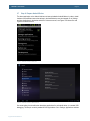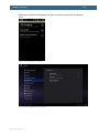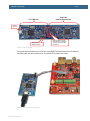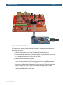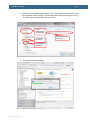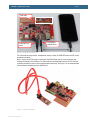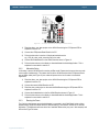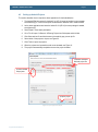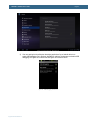
1
AOA Board rev A measurements mm measures [mil measures] 134.62 mm [5300 mil] 123.62 mm [4867 mil] 60.00 mm [2362 mil] 63.43 mm [2497 mil] 99.57 mm [3920 mil] 2.63 mm [104 mil] 17.78 mm [700 mil] 23.00 mm [906 mil] 25.00 mm [984 mil] 30.64 mm [1206 mil] 2.82 mm [111 mil] 33.27 mm [1310 mil] 5.50 mm [216.54 mil] 65.91 mm [2595 mil] 68.63 mm [2702 mil] 70.63 mm [2781 mil] 12.70 mm [500 mil] AOAA Kit - User’s Guide Copyright 2012 © Embedded Artists AB Android Open Accessory Application (AOAA) Kit User’s Guide Get Up-and-Running Quickly and Start Developing Your Application On Day 1! EA2-USG-1201 Rev A AOAA Kit - User’s Guide Page 2 Embedded Artists AB Davidshallsgatan 16 211 45 Malmö Sweden [email protected] http://www.EmbeddedArtists.com Copyright 2012 © Embedded Artists AB. All rights reserved. No part of this publication may be reproduced, transmitted, transcribed, stored in a retrieval system, or translated into any language or computer language, in any form or by any means, electronic, mechanical, magnetic, optical, chemical, manual or otherwise, without the prior written permission of Embedded Artists AB. Disclaimer Embedded Artists AB makes no representation or warranties with respect to the contents hereof and specifically disclaim any implied warranties or merchantability or fitness for any particular purpose. Information in this publication is subject to change without notice and does not represent a commitment on the part of Embedded Artists AB. Feedback We appreciate any feedback you may have for improvements on this document. Please send your comments to [email protected]. Trademarks All brand and product names mentioned herein are trademarks, services marks, registered trademarks, or registered service marks of their respective owners and should be treated as such. Copyright 2012 © Embedded Artists AB AOAA Kit - User’s Guide Page 3 Table of Contents 1 Document Revision History 5 2 Introduction 6 2.1 6 Features 2.1.1 LPC1769 side features 6 2.1.2 LPC11C24 side features 7 2.2 ESD Precaution 7 2.3 General Handling Care 8 2.4 Code Read Protection 8 2.5 CE Assessment 8 2.6 Other Products from Embedded Artists 8 2.6.1 Design and Production Services 8 2.6.2 OEM / Education / QuickStart Boards and Kits 8 3 Getting Started 9 3.1 Demo Applications 9 3.2 Step 1: Have Supported Android Devices 10 3.3 Step 2: Connect and Power the Board 11 3.4 Step 3: Verify Default Jumper Settings 12 3.5 Step 4: Install USB Driver for Console Output/ISP 12 3.6 Step 5: Download Demo Application 12 3.7 Step 6: Prepare Android Device 13 3.8 Step 7: Run the Demo Application 15 4 The AOAA Board Design 4.1 4.1.1 Copyright 2012 © Embedded Artists AB AOA Use Cases Industrial Use Case 16 16 17 4.2 CAN Network Expansion 19 4.3 RF Network Expansion 22 4.3.1 NXP’s/Jennic JN5148 module 22 4.3.2 Digi’s XBee family of radio modules 23 4.3.3 Serial Expansion Connector 23 4.4 Ethernet network expansion 23 4.5 Experiment Friendly 24 4.6 Hardware Block Diagram 25 4.7 Board Overview 26 4.8 Usage of CPU Pins 27 4.9 Schematic Walkthrough 31 4.9.1 Page 2 31 4.9.2 Page 3 31 4.9.3 Page 4 31 4.9.4 Page 5 31 4.9.5 Page 6 31 AOAA Kit - User’s Guide Page 4 4.9.6 Page 7 32 4.9.7 Page 8 32 4.9.8 Page 9 33 4.9.9 Page 10 33 5 Program Development 5.1 Program Download 34 5.1.1 ISP over UART Program Download 34 5.1.2 SWD/JTAG Program Download 36 Compiling the Demo Application 42 5.2 6 Troubleshooting Copyright 2012 © Embedded Artists AB 34 45 6.1.1 Cannot download/debug 45 6.1.2 Verify operation of board 45 7 Further Information 47 AOAA Kit - User’s Guide Page 5 1 Document Revision History Revision Date Description PA1 2012-01-28 First version. PA2 2012-02-10 Corrected grammar and smaller updates. A 2012-02-22 Added Android device to confirmed working list. PB1 2012-10-18 Clarified where to find USB connector J16. Copyright 2012 © Embedded Artists AB AOAA Kit - User’s Guide Page 6 2 Introduction Thank you for buying The Android™ Open Accessory Application Kit from Embedded Artists. For the rest of the document the term Android Open Accessory will be written out as AOA. The kit (hardware and software) will be called The AOAA Kit, for short. When referring to just the hardware the term AOAA Board will be used. The kit has been developed by Embedded Artists in close cooperation with NXP. It contains two microcontrollers from NXP, the LPC1769 (Cortex-M3 core) and LPC11C24 (Cortex-M0 core). The two microcontrollers are connected via a CAN network. This document is a User’s Guide that primarily describes the hardware design of the AOAA Board. Software development and Android specific issues are addressed in another document. 2.1 Features The AOAA kit from Embedded Artists lets you get up-and-running with AOA experiments immediately. It is a standalone platform for evaluation and prototyping electronic accessories for Google’s Android operating system. The AOAA kit is also suitable for experimenting with CAN, Ethernet and RF networks. Note that the AOAA board has been designed for evaluation and is not designed for final integration into consumer or industrial end-products. 2.1.1 LPC1769 side features NXP's LPC1769 ARM Cortex-M3 microcontroller in 100-pin LQFP package, with 64 KByte internal SRAM and 512 KByte internal FLASH. 12.0000 MHz crystal for maximum execution speed and standard serial bit rates, including USB and CAN requirements. The LPC1769 runs at frequencies up to 120 MHz. USB Host interface for Android connection USB Device interface Copyright 2012 © Embedded Artists AB Future proof for when Android devices can be USB Hosts also Other communication interfaces: 100/10Mbps Ethernet interface CAN interface (DSUB9 and RJ45 connector pads exist, not mounted per default) Serial Expansion Connector, 14-pos connector with UART/I2C/SPI/GPIO pins Pads for interfacing NXP/Jennic RF module (JN5148-XXX-M00) Socket for Digi™ XBee RF module and interface compatible modules IO and peripherals: Two RGB LEDs Two push buttons Analog input with trimming potentiometer Eight protected inputs/outputs (of which four can be analog inputs) Four open collector outputs (for driving for example relays) All free LPC1769 pins available on expansion connector UART-to-USB bridge that also supports automatic ISP (for program download via UART/USB) AOAA Kit - User’s Guide 32 kbit I2C E2PROM for storing non-volatile parameters Powered via Android device’s normal USB power plug +5V DC external supply can also be connected via standard 2.1mm power jack SWD/JTAG connector 2x5 pos, 50 mil/1.27 mm pitch, standard SWD/JTAG connector Small prototyping area 100 mil pitch matrix of holes, 64 x 23 mm in size Compact size of complete board: 135 x 100 mm (5.4 x 3.9 inch) 2.1.2 Four layer PCB design for best noise immunity LPC11C24 side features NXP's LPC11C24 ARM Cortex-M0 microcontroller in 48-pin LQFP package, with 8 KByte internal SRAM, 32 KByte internal FLASH and integrated CAN transceiver. 12.0000 MHz crystal for maximum execution speed and standard serial bit rates, including CAN requirements. The LPC11C24 runs at frequencies up to 50 MHz. Can be broken off from LPC1769 side of the board to create a remote CAN node. DSUB9 and RJ45 CAN interface Pads exist but connectors not mounted (only needed to expand CAN network or when LPC11C24 CAN node broken off from LPC1769 side). RGB-LED LED on PIO0_7 (compatible with LPCXpresso LPC11C24 board design) Push-button On wakeup pin (PIO1_4), allowing low-power experiments LM75 temperature sensor on I2C ISL29003 light sensor on I2C Powered via CAN interface +5V supplied, local 3.3V regulator on board All relevant LPC11C24 pins available on expansion connectors (dual 20 pos edge connector, 100 mil/2.54 mm pitch rows, 700 mil apart). SWD/JTAG connector 2.2 Page 7 2x5 pos, 50 mil/1.27 mm pitch, standard SWD/JTAG connector Compact size of LPC11C24 node: 69 x 23 mm (complete board is 135 x 100 mm) ESD Precaution Please note that the AOAA Board comes without any case/box and all components are exposed for finger touches – and therefore extra attention must be paid to ESD (electrostatic discharge) precaution. Copyright 2012 © Embedded Artists AB AOAA Kit - User’s Guide Page 8 Make it a habit always to first touch the metal surface of one of the USB or Ethernet connectors for a few seconds with both hands before touching any other parts of the boards. That way, you will have the same potential as the board and therefore minimize the risk for ESD. Note that Embedded Artists does not replace boards that have been damaged by ESD. 2.3 General Handling Care Handle the AOAA Board with care. The board is not mounted in a protective case/box and is not designed for rough physical handling. Connectors can ware out after excessive use. The board is designed for evaluation and prototyping use, and not for integration into consumer or industrial endproducts. 2.4 Code Read Protection The LPC1769 and LPC11C24 have a Code Read Protection function (specifically CRP3, see respective datasheets/user’s manuals for details) that, if enabled, will make the chip impossible to reprogram (unless the user program has implemented such functionality). Note that Embedded Artists does not replace AOA boards where the LPC1769 or LPC11C24 have CRP3 enabled. It’s the user’s responsibility to not invoke this mode by accident. 2.5 CE Assessment The AOAA Board is CE marked. See separate CE Declaration of Conformity document. The AOAA Board is a class B product. EMC emission test has been performed on the AOAA Board. Standard interfaces like Ethernet, CAN, USB, serial have been in use. General expansion connectors where internal signals are made available (for example processor pins) have been left unconnected. Connecting other devices to the product via the general expansion connectors may alter EMC emission. It is the user’s responsibility to make sure EMC emission limits are not exceeded when connecting other devices to the general expansion connectors of the AOAA Board. Due to the nature of the AOAA Board – an evaluation board not for integration into an end-product – fast transient immunity tests and conducted radio-frequency immunity tests have not been executed. Externally connected cables are assumed to be less than 3 meters. The general expansion connectors where internal signals are made available do not have any other ESD protection than from the chip themselves. Observe ESD precaution. 2.6 Other Products from Embedded Artists Embedded Artists have a broad range of LPC1000/2000/3000/4000 based boards that are very low cost and developed for prototyping / development as well as for OEM applications. Modifications for OEM applications can be done easily, even for modest production volumes. Contact Embedded Artists for further information about design and production services. 2.6.1 Design and Production Services Embedded Artists provide design services for custom designs, either completely new or modification to existing boards. Specific peripherals and I/O can be added easily to different designs, for example, communication interfaces, specific analog or digital I/O, and power supplies. Embedded Artists has a broad, and long, experience in designing industrial electronics in general and with NXP’s LPC1000/2000/3000/4000 microcontroller families in specific. Our competence also includes wireless and wired communication for embedded systems. For example IEEE802.11b/g (WLAN), Bluetooth™, ZigBee™, ISM RF, Ethernet, CAN, RS485, and Fieldbuses. 2.6.2 OEM / Education / QuickStart Boards and Kits Visit Embedded Artists’ home page, www.EmbeddedArtists.com, for information about other OEM / Education / QuickStart boards / kits or contact your local distributor. Copyright 2012 © Embedded Artists AB AOAA Kit - User’s Guide Page 9 3 Getting Started This chapter contains information about how to get acquainted with the AOAA Kit. Please read this chapter first before start using the board - it will be well spent time! 3.1 Demo Applications There are three AOA demo application that can be downloaded from the Embedded Artists support page. The AOAA board is not pre-loaded with any of these demo applications. The reason for this is that the applications are continuously updated and a pre-loaded application would quickly become outdated. Precompiled binary images (i.e., hex-files) can be downloaded from the support page. Note that there are two processors on the AOA board; the LPC1769 and LPC11C24. Normally it is only the LPC1769 that needs to be updated. The application on the LPC11C24 is the same for all demo applications and it is also pre-loaded during production test. The three AOA demo applications are: 1. Application that allows controlling and monitoring the AOAA Board (LPC1769 side) from an Android device. 2. Application where the Android device can detect CAN nodes (such as the LPC11C24 side of the AOAA board) in a CAN network. The CAN nodes can be controlled and monitored from the Android device. 3. Application where the Android device can detect XBee nodes in an XBee network. The XBee nodes can be controlled and monitored from the Android device. o XBee nodes are LPC1769 LPCXpresso Boards mounted on LPCXpresso Base Board. Code for this is also included. The demo applications include parts of well-known software packages like: FreeRTOS has been ported to the board and a demo is available that show how to use it. lwIP v1.4.0 has been ported to the board. The httpserver_raw (webserver) application from the lwIP contrib package is available with a small modification to use the on-board SD-card interface instead of the ROM based file system. FatFs file system module has been ported to the board. The lwIP demo (based on httpserver_raw) is using this module to access files on an SD card. nxpUSBlib is available and used in the AOA demos. Copyright 2012 © Embedded Artists AB AOAA Kit - User’s Guide Page 10 A seven step process will follow to get the one of the demo applications up-and-running quickly. 3.2 Step 1: Have Supported Android Devices Make sure to use an Android device that supports AOA. Not all Android devices support Android Open Accessory. A basic version requirement is to have Android version v3.1, or higher. Some v2.3.4 devices support Android Open Accessory but not all since the functionality has been back ported to this version and inclusion is optional. Below is a list of Android devices known to support the Android Open Accessory functionality. It is currently very short but will gradually be expanded when users report first hand success with specific devices. Please report firsthand experience to: [email protected] Brand Devices Acer Iconia A100 (tablet) Motorola Xoom (tablet) Samsung Galaxy Nexus (phone) HTC/Google Google Nexus One (phone) Below is a list of Android devices reported to support the Android Open Accessory functionality by others on Internet. Note that Embedded Artists has not tested the devices below. Brand Devices Acer Iconia A500 ASUS Eee Pad ASUS Eee Pad Transformer TF101 Foxconn Commtiva-HD710 Dell Streak 10 Pro HTC EVO 3D HTC PH4100 HTC Sensation 4G LG Optimus Pad LG Optimus 2X Samsung Galaxy A Samsung Galaxy Ace Samsung Galaxy S (S-II does not seem to work) Samsung Galaxy Tab 10.1 (might need some manual work to get it working) Samsung Galaxy S Sony Ericsson Xperia (Arc, Acro, Ray) Sharp IS05 Toshiba AT100 Copyright 2012 © Embedded Artists AB AOAA Kit - User’s Guide 3.3 Page 11 Step 2: Connect and Power the Board The picture below illustrates the basic setup of the AOAA board. The Android device is connected to the USB Host interface of the AOAA board, using the normal USB charger cable (that came with the Android device). The Android device’s charger is used to power the AOAA board. It actually also powers the Android device via the USB Host interface. The USB cable between the USB charger and the AOAA board is included in this kit. It is also possible to power the board via an external +5VDC, 1A power supply. Note that only one external source should power the AOA board at any given point in time. Android device charger (not included) The Android device (not included) USB-A to USB-B cable (included) Alternative external +5V supply (via standard 2.1 mm jack) Android Open Accessory with NXP’s LPC1769 USB-A to USB-micro B cable (not included) CAN node with LPC11C24 Figure 1 – The AOAA Board Setup Copyright 2012 © Embedded Artists AB Prototype area (100 mil pitch grid of holes) AOAA Kit - User’s Guide 3.4 Page 12 Step 3: Verify Default Jumper Settings Verify that the default jumper positions on the board are correct, as below. Figure 2 – The AOAA Board Default Jumper Positions 3.5 Step 4: Install USB Driver for Console Output/ISP The AOAA Board contains an USB-to-UART bridge chip (FT232R from FTDI) that connects UART channel #0 on the LPC1769 to a virtual COM port on the PC/laptop (via USB). This UART channel is typically used as the console channel for applications. Printf() output can for example be directed to this UART channel. To locate the (mini-B) USB connector, J16, see Figure 20. A USB driver must be installed on the PC/laptop in order for the virtual COM port to be created. See FTDI’s installation guides for details how to install the driver for different operating systems: http://www.ftdichip.com/Support/Documents/InstallGuides.htm 3.6 Step 5: Download Demo Application Download the selected demo application into the LPC1769. See section 5.1 for details how to download an application. For simplicity and quickest way forward, it is recommended to start with downloading via Flash Magic (i.e., using the UART-to-USB bridge). Precompiled binary images (i.e., bin-files) can be downloaded from the support page. There is no need to update the LPC11C24 application. It is pre-programmed with a suitable application from production test. Copyright 2012 © Embedded Artists AB AOAA Kit - User’s Guide 3.7 Page 13 Step 6: Prepare Android Device The demo application on the Android side has not been uploaded to Android Market. In order to install the demo from a different source the settings in the Android device must be changed. Go to Settings and then Applications in the device and check “Unknown sources”, see Figure 3 for Nexus One and Figure 4 for Motorola Xoom. Figure 3 – Unknown sources - Nexus One Figure 4 – Unknown sources – Motorola Xoom One more setting, that is useful when developing applications for an Android device, is to enable USB debugging. This step is not strictly needed for running the demo. Go to Settings, Applications and then Copyright 2012 © Embedded Artists AB AOAA Kit - User’s Guide Page 14 Development and enable USB debugging, see Figure 5 for Nexus One and Figure 6 for Motorola Xoom. Figure 5 – Enable USB debugging – Nexus One Figure 6 – Enable USB debugging – Motorola Xoom Copyright 2012 © Embedded Artists AB AOAA Kit - User’s Guide 3.8 Page 15 Step 7: Run the Demo Application 1. Connect the USB cable (USB micro-B to A) between the Android device and J3, if not already done. 2. A dialog will appear indicating that there is no installed application that work with the USB Accessory. Click the View button to download the application from Embedded Artists website. 3. When the application has been downloaded a dialog will appear asking if it is okay to install the application. Select Install. 4. After installation has completed it is possible to Open and start the application. 5. When the application starts allow it to access the USB accessory. Select OK. The demo application is now running on the Android device and communicating with the AOA board! Copyright 2012 © Embedded Artists AB AOAA Kit - User’s Guide Page 16 4 The AOAA Board Design This chapter describes the design of the AOAA Kit both from a conceptual and hardware perspective. Android Open Accessory allows connecting Accessories to an Android device. The Accessory and Android device communicates over USB. The Accessory has to implement a USB Host interface, while the Android acts as a USB client (also called USB Device). For more information about Android Open Accessory, see [3]. The AOAA Kit supports the requirements to implement an Android Accessory and much more! 4.1 AOA Use Cases Typical basic Accessory use cases are outlined below. There are many application where connecting (typically) a phone to an isolated system has great benefits. It can give the system a user interface for information readout or control of the system. It can also allow for the system to get Internet access. Graphical User Interface - For status readout from Accessory - For control of Accessory Phone is Internet gateway Android Accessory Device - For downloading new profiles/settings - For upgrading system - For buying new features - For accessing remote information - For allowing remote access of system, for example diagnostic service Accessory is gateway to wireless remote accessory, like pulse meter, pedometer, etc. Figure 7 – Basic Android Accessory Use Cases There are two ways of viewing the relationship between the Android device and the accessory: A traditional view is that the application in the Android device contains the intelligence and basically only uses the accessory for input/output. In a master/slave analogy, the Android device would be the master and the accessory the slave. An alternative is to view the Android device as (an alternative) user interface to the accessory. The intelligence is embedded in the accessory and the application running on the Android device creates a graphical user interface to the accessory. Possibly in combination with a communication channel with the Internet. The AOAA kit is much more than just a platform for prototyping and developing basic Android Open Accessory applications. The hardware has a network centric design, meaning that there is provision for creating both wired and wireless networks. Figure 8 below illustrated the three types of networks directly supported by the AOAA board. Copyright 2012 © Embedded Artists AB AOAA Kit - User’s Guide Page 17 Ethernet network ZigBee network or other RF network RF RF CAN network RF RF RF Figure 8 – The AOAA Board Network Interfaces A number of very powerful applications open up when the Accessory no longer is an isolated system, but instead a gateway to a networked system. The Android system no longer controls and interacts with just a single device, but a complete network! 4.1.1 Industrial Use Case Consider an industrial plant with a network of sensors diagnosing important components. It can for example be vibration and temperature monitoring of electrical motors. By being able to correctly diagnose and predict future failure of bearings and the motors in general, scheduled maintenance and service can be performed. Scheduled maintenance can prevent costly production stops. ”Smart motor” that signal warnings and alarms Sensors in network producing data to be gathered and analyzed by central controller Figure 9 – Advanced Android Accessory Use Case Copyright 2012 © Embedded Artists AB MOT135 needs lubrication MOT265 too high vibration MOT372 too high temperature Central controller with control intelligence and data gathering AOAA Kit - User’s Guide Page 18 The central controller (the AOAA board in this example) is connected to the Internet and can send diagnostic data to a service central, where maintenance is scheduled. A service technician can for example receive a message that immediate maintenance is needed for a specific motor. It can also be that maintenance is scheduled at a later point in time, but still urgent. Warnings and Alarms AOA SMS / email Network or “Smart Motors”, or any devices in general Figure 10 – Advanced Android Accessory Use Case, cont. When a service technician arrives at the Industrial plant, an Android device is connected to the central controller (since it is an Android Accessory also). For safety or security reasons, certain operations are only allowed on-site when the Android device is connected. An example can be firmware updates. The central controller normally operates in M2M mode (machine to machine communication) but it also acts as a user interface to the system when a service technician works with the system. The network can be of any type. CAN networks are common in Industrial plants due to the robustness of the CAN network. Wireless networks are also common when cabling cost and flexibility is an issue. The following three sections present the network interfaces in more detail. Copyright 2012 © Embedded Artists AB AOAA Kit - User’s Guide 4.2 Page 19 CAN Network Expansion The AOA board even contains an on-board CAN network. There is a CAN node built around the LPC11C24 microcontroller, which also contains an integrated CAN transceiver. The LPC1769 and LPC11C24 processors communicates over the CAN network. The CAN node can easily be detached from the main (LPC1769) board. If detaching the CAN node it is recommended to first cut the board connection between the CAN node and the prototype area. After that it is easier to cut off the CAN node. The location of the CAN network bridge is illustrated in the picture below. When cutting the network bridge, be sure to check that there are no shorts between the wires. DSUB9 expansion connector RJ45 expansion connector CAN network bridge – can be cut Step2: Cut these horizontal ones DSUB9 or RJ45 expansion connector (overlapping) Figure 11 – The AOAA Board Network Interfaces Figure 12 illustrated a CAN node that has been detached from the AOAA board. Copyright 2012 © Embedded Artists AB Step 1: Cut here AOAA Kit - User’s Guide Page 20 Figure 12 – CAN Node Detached from AOAA Board There is a possibility to extend the CAN network via either a DSUB9 (J6) or RJ45 (J5) connector. These connectors are not mounted but can easily be soldered, if needed. The connectors follow standard CAN pinning, see tables below. The CAN interface connectors on the LPC11C24 node are overlapping. Only one type of connector at a time can be used. The CAN network can be extended via normal Ethernet (cat 5 or cat 6) or DSUB-9 cabling. 9 pin Male DSUB 8 pin RJ45 Pin Signal Name Signal Description Pin Signal Name Signal Description 1 Reserved Upgrade path 1 CAN_H Dominant high 2 CAN_L Dominant low 2 CAN_L Dominant low 3 CAN_GND Ground 3 CAN_GND Ground 4 Reserved Upgrade path 4 Reserved Upgrade path 5 CAN_SHLD Shield, optional 5 Reserved Upgrade path 6 GND Ground, optional 6 CAN_SHLD Shield, optional 7 CAN_H Dominant high 7 CAN_GND Ground 8 Reserved Upgrade path 8 CAN_V+ Power, optional 9 CAN_V+ Power, optional Figure 13 illustrates how the CAN node can be removed from the AOAA board. An Ethernet cable and RJ45 connectors are used to create the CAN network. Copyright 2012 © Embedded Artists AB AOAA Kit - User’s Guide Page 21 Figure 13 – CAN Node via Ethernet Cable It is very simple to connect a CAN analyzer to AOAA board since standard CAN pinning is used on the DSUB9 connector. A standard DB9 F/F cable can be used. The Komodo™ from TotalPhase has been used during the development of the AOAA board with great success, see http://www.totalphase.com/products/komodo_canduo/ Figure 14 – CAN Analyzer Hookup Copyright 2012 © Embedded Artists AB AOAA Kit - User’s Guide 4.3 Page 22 RF Network Expansion There are two interfaces on the AOAA board for radio modules. One at a time can be used. Both types of radio modules exist in different (application) versions. This gives the flexibility to create different types of radio node networks, for example pure ZigBee network, proprietary network based on IEEE 802.15.4, WiFi (IEEE802.11abgn) and 6LowPAN with different underlying radio standards. The network topology can be point-to-multipoint or mesh, depending on how the used radio modules are programmed. The flexibilities are endless! XBee socket NXP/Jennic pads on top side on bottom side General expansion connector with SPI, UART, etc. Figure 15 – Radio Module Interfaces on the AOAA Board 4.3.1 NXP’s/Jennic JN5148 module The interface to this module is on the bottom side of the board. Two alternatives are supported; either direct soldering to pads on the pcb or mounting on pin headers. The pin headers must be soldered to the board manually. Note that these pin headers are not included. The pin headers match the JN5148 modules that are shipped with Jennic’s/NXP’s evaluation kits. Figure 16 illustrates a radio module that has been soldered to the bottom side of the AOAA board. Figure 16 – NXP/Jennic Radio Module Mounting on Bottom Side Copyright 2012 © Embedded Artists AB AOAA Kit - User’s Guide Page 23 There is support for application download into the JN5148 module via a FTDI UART-to-USB cable that is connected to pin header J8. 4.3.2 Digi’s XBee family of radio modules The interface to this module is located on the top/component side of the board. The form factor is simple to use and program and there are many different versions of the module. Note that there are also several radio modules on the market that build upon the same form factor as the Digi’s XBee module. Figure 17 illustrates how the XBee module is mounted in the socket on the top side of the AOAA board. One of the demo applications for the AOAA board uses XBee Series 1 modules. Figure 17 – Radio Module Interfaces on the AOAA Board 4.3.3 Serial Expansion Connector It is also possible to add radio modules via the Serial Expansion Connector. This universal interface connector contains SPI/UART/I2C/GPIO interfaces. Some radio modules on the market prefer to use the SPI interface instead of UART communication (which is used for the two main radio module interfaces on the AOAA board). 4.4 Ethernet network expansion The Ethernet interface is very straightforward. It supports 100/10 Mbps operation, auto-negotiation and HP Auto-MDIX. There is an lwIP port for the board that is a good starting point for creating TCP/IP networks on top the Ethernet network. Besides creating local Ethernet networks the AOAA board can be connected to Internet gateways for global Internet access. Copyright 2012 © Embedded Artists AB AOAA Kit - User’s Guide 4.5 Page 24 Experiment Friendly The AOAA board is very experiment and prototype friendly. There are a lot of on-board peripherals and good expansion possibilities on the AOAA board. Below is a list of highlights: Input Three RGB LEDs and individual LEDs Three push buttons √ Analog input with trimming potentiometer √ Eight protected inputs/outputs (of which four can be analog inputs) √ Four open collector outputs (for driving for example relays) All free LPC1769 pins available on expansion connector √ LM75 temperature sensor √ ISL29003 light sensor √ All LPC11C24 pins available on expansion connector √ Output √ √ √ √ √ The demo applications showcase some of the on-board peripherals. For more information about the demo applications, see section 3.1 . The on-board prototype area cannot be missed on the AOAA board. It is located in the lower right corner of the board. There is a 100 mil pitch grid of 1.05mm holes. Copyright 2012 © Embedded Artists AB AOAA Kit - User’s Guide 4.6 Page 25 Hardware Block Diagram The block diagram in Figure 18 below gives a quick overview of a design. It illustrates the major components in the design. The center of the design is the LPC1769 MCU from NXP. There is a USB Host interface to the Android device as well as several other communication interfaces. The design also contains a CAN node, built around the LPC11C24 MCU from NXP. It contains an integrated CAN transceiver. The board is powered from an external +5V supply (typically the Android device’s USB charger). USB Device interface USB Host interface Select +5V RF-module interface (NXP/Jennic and XBee) Ethernet interface LPC1769 UART-to-USB bridge with automatic ISP func. Prototype area +5V to CAN network +3.3V Expansion connectors IO and Peripherals Power input (USB or +5V) CAN interface SWD I/F uSD memory card interface (via SPI) CAN network CAN node side +3.3V Expansion connector Temperature and Light sensors on I2C I2C Power supply LPC11C24 CAN microcontroller LEDs and push button SWD I/F Figure 18 – The AOAA Board Block Diagram Both MCUs have SWD interfaces for program download. The LPC1769 also supports program download via UART (there is an UART-to-USB bridge that also support automatic ISP activation). Copyright 2012 © Embedded Artists AB AOAA Kit - User’s Guide 4.7 Page 26 Board Overview Figure 19 below illustrates the board structure. The upper part is the LPC1769 side of the design. The lower part contains the LPC11C24 CAN node and a prototype area. uSD interface Communication interfaces (Ethernet, USB H/D, RF modules) and power input LPC1769 side CAN connectors LPC11C24 CAN node Prototype area Figure 19 – The AOAA Board Overview Figure 20 below is a more detailed illustration of the board structure with key components, connectors and jumpers marked. Copyright 2012 © Embedded Artists AB AOAA Kit - User’s Guide J4, Ethernet connector Page 27 J2,USB Device connector J2,USB Host connector J14,USB-B power input J15,power input (alt +5V) RF2,XBee socket RF1,JN5148 pads on bottom side J22,uSD connector JP1/JP2 up (pos1-2)= USB Device down (pos2-3)=USB Host J16, UARTto-USB i/f J8 JP3 J1, SWD i/f for LPC1769 R93, trim.pot. JP4 J13, 8 prot. I/O J7, serial exp. connector J11, 4 OD I/O Top-to-bottom: LED6 / SW2 LED7 / SW3 SW5, pushbutton J12, expansion connector SW4, Reset J21, SWD i/f for LPC11C24 LED12, RGB-LED Figure 20 – The AOAA Board Overview, part 2 4.8 Usage of CPU Pins The table below lists how the LPC1769 pins are used in the design and which ones are available on the expansion connector, J12. LPC1769 pin Usage P0_0, P0_1 CAN interface P0_2, P0_3 UART#0 connected to UART-to-USB bridge P0_4 Not used, free for expansion Pin 1 P0_5 Not used, free for expansion Pin 3 P0_6 – P0_9 SPI#1 connected to uSD interface and serial expansion connector. Pin 5 (P0_6), Pin 7 (P0_7), Pin 9 (P0_8), Copyright 2012 © Embedded Artists AB Expansion connector (J12) AOAA Kit - User’s Guide Page 28 Pin 11 (P0_9) P0_10 Connected to protected IO, pin 5 of J13 Pin 13 P0_11 connected to protected IO, pin 6 of J13 Pin 15 P0_15, P0_16 UART#1 connected to RF modules P0_17 Optionally connected to XBee module as CTS signal Pin 17 P0_18 Power control of uSD interface and connected to protected IO, pin 7 of J13 Pin 19 P0_19 Card detect input from uSD interface Pin 21 P0_20 Optionally connected to XBee module as DTR signal Pin 23 P0_21 Not used, free for expansion Pin 25 P0_22 Optionally connected to XBee module as RTS signal Pin 27 P0_23 Analog inputs #0 connected to serial expansion connector and protected IO, pin 1 of J13 Pin 29 P0_24 Analog inputs #1 connected to protected IO, pin 2 of J13 Pin 31 P0_25 Analog inputs #2 connected to protected IO, pin 3 of J13 Pin 33 P0_26 Analog inputs #3 or analog output connected to serial expansion connector and connected to protected IO, pin 4 of J13 Pin 35 P0_27, P0_28 I2C interface connected to serial expansion connector and E2PROM Pin 37 (P0_27), Pin 39 (P0_28) P0_29, P0_30 USB interface, either Host or Device P1_0 – P1_17 Ethernet interface P1_18 USB UP LED control P1_19 USB Host power control P1_20 Not used, free for expansion Pin 41 P1_21 Not used, free for expansion Pin 2 P1_22 USB Host VBUS monitor input P1_23 Connected to open drain output OUT1 of J11 Pin 4 P1_24 Connected to open drain output OUT2 of J11 Pin 6 P1_25 Connected to open drain output OUT3 of J11 Pin 8 P1_26 Connected to open drain output OUT4 of J11 Pin 10 P1_27 USB Host distribution switch over-current status input P1_28 Not used, free for expansion Pin 12 P1_29 Not used, free for expansion Pin 14 P1_30 USB Device VBUS input P1_31 Analog input #5 connected to trimming pot. R93 Copyright 2012 © Embedded Artists AB AOAA Kit - User’s Guide Page 29 P2_0 Connected to red LED in RGB-LED D6 Pin 16 P2_1 Connected to blue LED in RGB-LED D6 Pin 18 P2_2 Connected to green LED in RGB-LED D6 Pin 20 P2_3 Connected to red LED in RGB-LED D7 Pin 22 P2_4 Connected to blue LED in RGB-LED D7 Pin 24 P2_5 Connected to green LED in RGB-LED D7 Pin 26 P2_6 Not used, free for expansion Pin 28 P2_7 Not used, free for expansion Pin 30 P2_8 Not used, free for expansion Pin 32 P2_9 USB Device connection control P2_10 Boot load enable input controlled from automatic ISP function of UART-to-USB bridge P2_11 Connected to push button SW2 (KEY1) P2_12 Connected to push button SW3 (KEY2) P2_13 Connected to protected IO, pin 8 of J13 Pin 36 P3_25 Connected to serial expansion connector Pin 38 P3_26 Connected to serial expansion connector Pin 40 P4_28 – P4_29 UART#3 connected to serial expansion connector Pin 42 (P4_28), Pin 44 (P4_29) Ground Power supply Pin 46, 48, 50 RESET_IN Reset input to LPC1769 Pin 43 VREF Reference voltage to ADC of LPC1769 (is an output, no external voltage should be supplied to this pin) Pin 45 +3.3V Power supply Pin 47 +5V Power supply Pin 49 Pin 34 The table below lists how the LPC11C24 pins are used in the design and where the pins are available on the expansion connector pair, J19/J20. LPC11C24 pin Usage Expansion connectors (J19/20) PIO0_0 Reset J19, pin 1 PIO0_1 Not used, free for expansion J19, pin 2 PIO0_2 Not used, free for expansion J19, pin 3 PIO0_3 Connected to interrupt output of light sensor J19, pin 4 PIO0_4 I2C-SCL connected to temperature and light sensors J19, pin 5 PIO0_5 I2C-SDA connected to temperature and light sensors J19, pin 6 PIO0_6 Not used, free for expansion J19, pin 7 Copyright 2012 © Embedded Artists AB AOAA Kit - User’s Guide Page 30 PIO0_7 Connected to LED13 J19, pin 8 PIO0_8 Connected to red LED of RGB-LED D12 J19, pin 9 PIO0_9 Connected to blue LED of RGB-LED D12 J19, pin 10 PIO0_10 Connected to green LED of RGB-LED D12 J19, pin 11 PIO0_11 Not used, free for expansion J19, pin 12 PIO1_0 Not used, free for expansion J19, pin 13 PIO1_1 Not used, free for expansion J19, pin 14 PIO1_2 Not used, free for expansion J19, pin 15 PIO1_3 Not used, free for expansion J19, pin 16 PIO1_4 Connected to push button SW5 (KEY3) J19, pin 17 PIO1_5 Not used, free for expansion J19, pin 18 +5V supply from CAN network J19, pin 19 Ground J19, pin 20 PIO1_6 Not used, free for expansion J20, pin 1 PIO1_7 Not used, free for expansion J20, pin 2 PIO1_8 Not used, free for expansion J20, pin 3 PIO1_9 Not used, free for expansion J20, pin 4 PIO1_10 Not used, free for expansion J20, pin 5 PIO2_0 Not used, free for expansion J20, pin 6 PIO2_1 Not used, free for expansion J20, pin 7 PIO2_2 Not used, free for expansion J20, pin 8 PIO2_3 Not used, free for expansion J20, pin 9 PIO2_6 Not used, free for expansion J20, pin 10 PIO2_7 Not used, free for expansion J20, pin 11 PIO2_8 Not used, free for expansion J20, pin 12 PIO2_10 Not used, free for expansion J20, pin 13 PIO2_11 Not used, free for expansion J20, pin 14 PIO3_0 Not used, free for expansion J20, pin 15 PIO3_1 Not used, free for expansion J20, pin 16 PIO3_2 Not used, free for expansion J20, pin 17 PIO3_3 Not used, free for expansion J20, pin 18 Local +3.3V supply generated from +5V J20, pin 19 Ground J20, pin 20 Copyright 2012 © Embedded Artists AB AOAA Kit - User’s Guide 4.9 Page 31 Schematic Walkthrough 4.9.1 Page 2 The center of the AOAA board is the LPC1769 from NXP. It is a MCU based on the ARM Cortex-M3 core. LPC1769 has many communication interfaces, which are used on the AOAA board. The external crystal is 12MHz, which is the recommended value to get standard CAN timing and meeting the USB frequency requirements. The RTC crystal is not mounted since AOAA board is not a low-power design. It will always be powered. The RTC can derive its clock from the main oscillator. J1 is the SWD interface for LPC1769, i.e., debug interface. It is the new and smaller footprint standard ARM debug connector. It has 2x5 pins in 50 mil pitch. 4.9.2 Page 3 The LPC1769 has one USB port that can act as either device or host. The AOAA board contains one USB Device interface and one USB Host interface. At any given point in time, one of them can be used. JP1/JP2 selects which USB interface the LPC1769 USB port is connected to. The USB Device interface is very straight forward and consists of a USB-B connector (J2), ESD protection, VBUS sense and DP pull-up resistor control. The USB Host interface is also very straight forward and consists of a USB-A connector (J3), ESD protection, VBUS distribution switch (U2) and VBUS/distribution switch status sense. 4.9.3 Page 4 The LPC1769 Ethernet interface is connected to an external Ethernet PHY (U3), LAN8720 from SMSC, via the standard RMII interface. The LAN8720 chip generates the needed 50MHz clock from an external 25MHz crystal. The RJ45 connector (J4) contains integrated magnetic. There is a 32kbit I2C E2PROM (U5) for storing non-volatile parameters, like MAC address. The I2C address to the 24LC32AT chip is 0xA0 (1.0.1.0.0.0.0.rw). Details about the 24LC32AT chip operation can be found in the datasheet. 4.9.4 Page 5 The LPC1769 CAN interface is connected to an external CAN transceiver (U6). The on-board CAN network connects directly to the LPC11C24 CAN node. There is a possibility to extend the CAN network via either a DSUB9 (J6) or RJ45 (J5) connector. These connectors are not mounted but can easily be soldered, if needed. The connectors follow standard CAN pinning. The Serial Expansion Connector (J7) is a 14-pin standardized connector on Embedded Artists boards. The connector carries UART/I2C/SPI/GPIO signals, allowing for flexible expansion to external devices. 4.9.5 Page 6 UART#1 of the LPC1769 can be connected to a radio module. Two interfaces are supported: NXP’s/Jennic JN5148 module The interface to this module is on the bottom side of the board. Two alternatives are supported; either direct soldering to pads on the pcb or mounting on pin headers. The pin headers must be soldered to the board manually. Note that these pin headers are not included. The pin headers match the JN5148 modules that are shipped with Jennic’s/NXP’s evaluation kits. o Copyright 2012 © Embedded Artists AB There is support for application download into the JN5148 module. Connect a FTDI UART-to-USB cable (FTDI part no. TTL-232R-3V3, Digikey part no. 768-1015-ND) to J8 and keep SW1 pressed while pressing and releasing the reset push button, SW4. The JN5148 modules in now in a bootload mode accepting application download via Jennic’s/NXP’s flash download application. AOAA Kit - User’s Guide Page 32 o All pins of the JN5148 modules are not connected. Only the ones needed to get a UART communication channel with the board. Digi’s XBee family of radio modules The interface to this module is located on the top/component side of the board. There are two 1x10 pos, 2mm pitch sockets for inserting the XBee module. o Only the pins needed for UART communication have been connected to the LPC1769. There is an option to use three data flow modem signals also (RTC, CTS and DTR) via JP3. All pins of the XBee module is accessible connectors J9 and J10 that are located just beside the XBee modules. o Three LEDs have been added that can signal different states of the operation. Note that only one module at a time can be connected. There are different (application) versions of the radio modules which gives the flexibility to create different types of radio node networks. There are also several radio modules that build upon the same form factor as the XBee module. 4.9.6 Page 7 There is a uSD memory card interface connector, J22. The memory card can be accessed via the SPI peripheral, which is 1-bit serial. The higher-throughput 4-bit parallel interface that also exists on these memory cards cannot be used. There is a voltage switch implemented by a p-channel mosfet (Q9) controlled by signal P0.18. LED14 is on when the uSD interface is powered. LED15 is on when a uSD memory card is inserted into the (J22) connector and this can also be detected via signal P0.19. A low signals indicated that a uSD memory card is inserted. 4.9.7 Page 8 There are some basic peripherals in the design for direct prototyping/experimenting with the AOAA application. There are also general expansion interfaces for external circuits. As basic peripherals there are: Two RGB-LEDs (LED6 and LED7) are connected to PWM outputs of the LPC1769. Two push buttons are connected to interrupt inputs of the LPC1769. A trimming potentiometer (R93) is connected to analog input #5 of the LPC1769. For general expansion there are: Eight protected inputs/outputs. The I/Os are protected with series resistors, filtering capacitors and clamping diodes. Four open drain outputs. These outputs can be used to drive relays and opto-couplers for controlling larger loads. There are clamping diodes that can be connected to the external power supply (pin 5 of J11), typically a 5, 12, or 24 supply. Check the BSH111 datasheets for details about switching capabilities. Expansion connector (J12) that contains all available LPC1769 pins – ‘available’ in the sense of not used for other purposes. These LPC1769 pins are directly connected to the connector and there is no protection. Pins that have dedicated use on the AOA board are not included in the connector. Note that some of the pins on the expansion connector can be used by other functionalities on the board but the user can select to not make use of these functions. For example, the SPI interface is used by the uSD memory card interface and the PWM signals control the RGB-LEDs. It is still however possible to use the SPI and PWM interface for external expansion via J12. Copyright 2012 © Embedded Artists AB AOAA Kit - User’s Guide 4.9.8 Page 33 Page 9 The board is normally powered via J14, a USB-B connector where the Android device’s charger is connected. Alternatively an external +5VDC, 1A supply can be connected via J15, a 2.1mm power jack input. The power supply is very simple, an LDO to create the +3.3V from the +5V input. There is a UART-to-USB bridge based on the FT232RL chip from FTDI. It is connected to UART#0 on the LPC1769. When inserting both jumpers in JP4 (pin 1-2 and 3-4) the automatic ISP activation functionality is enabled. The modem signals RTS and DTS modem can control reset and pulling pin P2.10 low, hence enabling In-System Programming (ISP) mode. It is an internal boot loader mode for downloading code into the LPC1769 over the UART. The PC application FlashMagic (http://www.flashmagictool.com) can be used for this. Voltage supervisor, U12, generate a proper reset to the system. Reset-LED LED11 is on whenever reset is active. There is also a Reset push button, SW4 for generating manual resets. 4.9.9 Page 10 The last schematic page contains the LPC11C24 CAN node. It is a separate part f the design on the sense that it is physically separated on the pcb and the only connection to the LPC1769 is via the onboard CAN network. The LPC11C24 CAN node can be broken off from the AOA board. The node can still be connected to a CAN network via a DSUB9 (J18) or RJ45 (J17) connector. Note that these connectors are overlapping on the board so only one can be used at a time. These connectors are not mounted but can easily be soldered, if needed. The connectors follow standard CAN pinning. The center of the CAN node is the LPC11C24 from NXP. It is a MCU based on the ARM Cortex-M0 core and has integrated CAN transceiver in the package. The external crystal is 12MHz, which is the recommended value to get standard CAN timing. The CAN node is powered via the +5V supply that is part of the CAN network. LDO U13 generates the needed local +3.3V supply. There are two sensors connected to the I2C channel: The ISL29003 ambient light sensor from Intersil. The I2C address to the ISL29003 is 0x44 (1.0.0.0.1.0.0.rw). Details about the ISL29003 operation can be found in the datasheet. The LM75B temperature sensor is from NXP. The I2C address to the LM75B is 0x48 (1.0.0.1.0.0.0.rw). Details about the LM75B operation can be found in the datasheet. There is an RGB-LED, LED12 as well as a single LED, LED13. There is also a push button, SW5, connected to pin PIO1_4. This is the wakeup input to the LPC11C24, which can be useful if experimenting with the power down modes of the MCU. J21 is the SWD interface for LPC11C24, i.e., debug interface. It is the new and smaller footprint standard ARM debug connector. It has 2x5 pins in 50 mil pitch. All pins of the LPC11C24 are available on the edge expansion connectors, J19 and J20. These are 2.54mm/100 mil pitch connectors placed 17.78 mm / 700 mil apart. Copyright 2012 © Embedded Artists AB AOAA Kit - User’s Guide Page 34 5 Program Development This chapter describes how to download code to the AOAA board and how to compile the demo applications – and in the extension, how to develop own demo applications. Details of the demo applications are not described in this document. 5.1 Program Download The AOAA board contains two processors, the LPC1769 and LPC11C24. Both supports program download via SWD/JTAG. The LPC1769 additionally supports program download via ISP over UART (the USB-to-UART bridge is used). The two methods are briefly described below: ISP over UART ISP is short for In-System Programming. The LPC1769 contains a bootloader in ROM that can be enabled by pulling pin P2.10 low during reset. The application can then be downloaded over UART#0 (serial channel). An application is needed on the PC for downloading the application code. SWD/JTAG There are many different SWD/JTAG interfaces on the market. NXP has created LPC-LINK. Keil has ULINK. IAR/Segger has JLINK. Code Red has Red Probe, etc. There is also OpenOCD, which is an open source project. Consult the respective manual for the SWD/JTAG interface used to get instructions how to download a hex/binary file. It is assumed that a binary image exist that represent the application program. This file is often a so called hex-file, which is a file format that Intel created a long time ago. It can also be a pure binary file (then typically called a bin-file). The Embedded Artists support site contains pre-compiled hex/bin-files of the demo applications. Section 5.2 describes how to compile the demo application, in order to generate the hex-file. 5.1.1 ISP over UART Program Download There are two jumpers (JP4) on the AOAA Board related to the USB-to-UART serial channel control signals and automatic ISP functionality. See Figure 20 for details about where the USB connector and jumpers are located. Normally the two jumpers in JP4 shall be inserted. However, sometimes the terminal program on the PC/laptop can resets the board and/or enable ISP mode by accident. If this happens, just remove the two JP4 jumpers. When downloading code via ISP mode, the two jumpers in JP4 shall however be inserted. This way, the application on the PC for downloaded the application code can automatically enable ISP mode. Download and install Flash Magic (http://www.flashmagictool.com/). This application directly supports application download via ISP (and can automatically enable ISP also). Copyright 2012 © Embedded Artists AB AOAA Kit - User’s Guide Page 35 Some settings must be changed in Flash Magic in order to enable automatic enabling of ISP. Figure 21 illustrates where the Advanced Options selection can be found. Figure 21 – Flash Magic Advance Options Then select the Hardware Config tab end set checkboxes and T1/T2 numbers according to Figure 22. Figure 22 – Flash Magic Hardware Config Copyright 2012 © Embedded Artists AB AOAA Kit - User’s Guide Page 36 After this, Flash Magic is ready to be used. Start by selecting the correct device, LPC1769 in this case. Then select the correct COM port. Note that the AOAA board contains a UART-to-USB bridge. UART#0 of the LPC1769 is connected to this. See section 3.5 how to install the driver for this bridge chip. When the AOAA board is connected via a USB cable (J16, mini-B USB connector) to the PC a (virtual) COM port will be created. It is this COM port that shall be selected. Baud rate shall be set to “57600”, Interface to “None (ISP)” and Oscillator to “12”. Sometimes the baud rate must be lowered to “38400” to get it working. If there is problem to communicate with the board, test to lower the baud rate first. After this, select the hex/binary file to be downloaded. Finally press the Start button to start downloading the application. Figure 23 – Flash Magic 5.1.2 SWD/JTAG Program Download This section describes how to download an application with the help of LPCXpresso IDE and the LPCLINK. For other development environments (IDEs), see respective documentation about flashing. The first thing is to create an LPC-LINK, the SWD/JTAG interface that the LPCXpresso IDE uses. It is a relatively simple process. Start with an LPCXpresso LPC1769 board. Separate the LPC-LINK side from the target side either by physically cutting the board or by using a soldering iron and remove all solder bumps that form the connection between the two sides. See Figure 24 for an illustration. The reason why an LPCXpresso LPC1769 board is recommended is that not all LPCXpresso boards have the same connections between the two sides. The LPC1769 board is very simple to separate with a soldering iron. Copyright 2012 © Embedded Artists AB AOAA Kit - User’s Guide Page 37 LPC-LINK side Target side (shall be disconnected) Connect to USB on PC Resulting SWD/JTAG interface connector Separate either by physically cutting the board, or simpler by removing solder bumps with a soldering iron. Figure 24 – Create an LPC-LINK The pictures below illustrate how to connect the 10-pos SWD/JTAG cable between the LPC-LINK and the AOAA board. Note the orientation of the 10-pos SWD/JTAG cable in both cases. Figure 25 – Connect LPC-LINK to the LPC1769 Copyright 2012 © Embedded Artists AB AOAA Kit - User’s Guide Page 38 Figure 26 – Connect LPC-LINK to the LPC11C24 Below are the steps to perform a program download. Normally the demo projects would be opened in the LPCXpresso IDE and then program download is very simple. The description below assumes no demo project that is active. 1. Make sure that the latest version of the LPCXpresso IDE is installed on the PC. 2. Connect a USB cable between the LPC-LINK and the PC, see Figure 24 above. Connect the 10-pos SWD/JTAG cable between the LPC-LINK and the debug connector of the processor to be programmed (either the LPC1769 or the LPC11C24). 3. Make sure that the AOAA board is powered. 4. Make sure the processor to be programmed is in a mode where the debugger can take control over the processor. This is normally the case, but if the current application uses lowpower modes there is a possibility that the SWD/JTAG interface is not enabled. If so, place the processor in ISP bootload mode (keep pin P2.10 low on the LPC1769 while resetting the board or keep pin PIO0_1 low on the LPC11C24 while powering up the AOAA board). 5. Click on the "Program Flash" icon from the tool bar, see picture below. The icon can be at different places depending on window size. Copyright 2012 © Embedded Artists AB AOAA Kit - User’s Guide Page 39 Program Flash Icon Figure 27 – LPCXpresso IDE Program Flash Icon 6. The next step is to select which processor to download to. Select LPC1769 or LPC11C24, depending on which processor to program. Then press OK button. Note that this step is sometimes not needed because the LPCXpresso IDE can itself detect which processor it is connected to. Note that the LPCXpresso is code size limited and the LPC1769 has bigger flash than the 128kByte limit. This message can be ignored and applications up to 128kByte can be downloaded. Above that, a less restrictive license of the LPCXpresso IDE must be bought from Code Red Technologies. There seems to be a small bug and it might be needed that the desired processor must be selected twice. Copyright 2012 © Embedded Artists AB AOAA Kit - User’s Guide Figure 28 –LPCXpresso IDE Target Selection 7. The next step is to browse to the file to download. Press the “Browse” button. Figure 29 – LPCXpresso IDE Program Flash Window Copyright 2012 © Embedded Artists AB Page 40 AOAA Kit - User’s Guide Page 41 8. Browse to the pre-compiled program images. If it is in fact the demo projects that exist, select the top directory and then “Debug”. In this subfolder there is either a file ending with *.axf or *.bin. Select one of these files. Press the “Open” button. 1) Find workspace and all sample apps. 2) Find project top directory 3) Find “Debug” subdirectory Figure 30 – Browse to File to Download 9. The program will start downloading. Figure 31 – LPCXpresso IDE Program Flashing in Progress Copyright 2012 © Embedded Artists AB 4) Select either *.axf or *.bin file AOAA Kit - User’s Guide Page 42 10. In case flashing fails, an error message like below will be displays. This is an indication that the debugger could not connect to the LPC1769 or LPC11C24. The most common reason is that the microcontroller was in a low-power mode where debug connection is not possible. Make sure the microcontroller is in ISP/bootload mode and try again. Also make sure the small 10-pos flat cable is correctly connected. Figure 32 – LPCXpresso IDE Program Failing to Flash 5.2 Compiling the Demo Application This section describes how to compile the demo application or any other sample application in general. A separate document about the AOAA board software describes the details. The demo applications have been developed in the LPCXpresso IDE. This is what is described. There are introduction videos and presentation about how to get started with the LPCXpresso IDE on the LPCXpresso website, see [8]. First make sure that the latest version of the LPCXpresso IDE is installed. Secondly, start the LPCXpresso IDE and select a new (and empty) workspace directly. Third, import the package of sample application projects into the Eclipse workspace. The package can be downloaded (as a zip-file) from Embedded Artists support page after registering the product. The zip-file contains all project files and is a simple way to distribute complete Eclipse projects. Select the Import and Export tab in the Quickstart menu and then Import archived projects (zip), see figure below. Copyright 2012 © Embedded Artists AB AOAA Kit - User’s Guide Page 43 1) Select Import and Export 2) Select Import archived projects (zip) Figure 33 – LPCXpresso IDE Import Archived Project Next, browse and select the downloaded zip file containing the archived sample applications. Select the sub-projects to be imported, see figure below (note that the screen shot below is generic and the project names will be different in the AOA demo applications). 1) Browse and select archived project file 2) Select wanted sub-projects 3) Import project Figure 34 – LPCXpresso IDE Import Archived Project Window Copyright 2012 © Embedded Artists AB AOAA Kit - User’s Guide Page 44 The selected projects are now imported. Click (to select) the project to work with. Browse and edit the project files. Build/clean/debug the project from the Quickstart menu (Start here), see picture below. When debugging a project, make sure the AOAA board is connected via LPC-LINK to the PC because the application will be downloaded to the board via LPC-LINK (SWD debug interface). 1) Click (to select) main project 2) Browse and edit project files 3) Build/clean/debug project Figure 35 – LPCXpresso IDE Build/Debug Project When the code has been downloaded execution will stop at the first line in the main function. Press F8 on the computer keyboard to resume/start execution. Copyright 2012 © Embedded Artists AB AOAA Kit - User’s Guide Page 45 6 Troubleshooting This chapter contains information about how to troubleshoot boards that does not seem to operate properly. It is strongly advised to read through the list of tests and actions that can be done before contacting Embedded Artists support. The different tests can help determine if there is a problem with the board, or not. For return policy, please read Embedded Artists’ General Terms & Conditions document. This document can be found on the Embedded Artists’ web site. 6.1.1 Cannot download/debug Symptom: Cannot contact the LPC1769 or LPC11C24 via SWD Check powering, check that the SWD interface works on another board. Cause: An erroneous application program can disable the SWD interface and/or program the internal clocks in the wrong way so that it is impossible to download a new application to the board. The erroneous application program starts executing after a reset and initializes the LPC1xxx in the wrong way before an external debugger can get control over the processor. Solution: Use FlashMagic on the LPC1769 to erase the flash completely. On the LPC11C24, pull PIO0_1 low while power cycling the board (= resetting the LPC11C24). This way the ‘known good’ internal bootloader starts executing. From this state, it is possible for an external debugger to get control over the processor and download a new application program. 6.1.2 Verify operation of board Symptom: The AOAA board does not seem to operate properly. Solution: Perform a complete verification of the board. The first step is to make sure that powering works properly. Make sure that all jumpers are in their default position, see section 3.4 for details. Connect a USB charger to J14 (or an external +5VDC, 1A supply to J15). Test points TP2, TP3 and TP4 are located just above the LPC1769. Measure the voltage between TP3 and TP4. The voltage shall be between 4.5 and 5.5V. Measure the voltage between TP2 and TP4. The voltage shall be between 3.15 and 3.34V. The second step is to download the production test application into the board. Since there are two processors on the AOAA board, both needs to be programmed. Normally the LPC11C24 (CAN node) is not changed so the default application is most likely still programmed on this processor. See section 5.1 for details how to download an application. 1. The following material is needed to perform a full test of the board: USB cable (mini-B to A) for console output Ethernet cable USB keyboard Micro SD card with the file testfile.txt (see zip-file from support page when downloading the test application). 2. Prepare the AOAA board for test: Copyright 2012 © Embedded Artists AB Connect the USB cable (B to A) to an USB charger or external power supply Connect the USB cable (mini-B to A) to a PC Connect the Ethernet cable to a PC (preferably local connection – the PC shall not be connected to a network) Connect a USB keyboard to the USB Host connector of the AOAA board. AOAA Kit - User’s Guide Page 46 Start a terminal application on the PC. TeraTerm works fine. Use 115200 bps, 8N1 and select the COM port that pops up when the USB cable from the AOAA board is connected to the PC. 3. Press the reset push-button, SW4 and observe the console output in the terminal window on the PC. The following tests will be performed: Copyright 2012 © Embedded Artists AB E2PROM test; an automatic test. CAN test; an automatic test Ethernet test; the test expects to Ping requests to be sent to the board. The IP address is written to the console. Start a command prompt and write ping -t 192.168.5.241 if you would like to ping 192.168.5.241 continually. Two ping requests are expected to be received. uSD memory card test; The file testfile.txt will be read from the SD card and the content verified. SW2 and SW3 test; Press SW2 and SW3 button for this test to pass. Trimming potentiometer test; Turn the trimming potentiometer to its end-points. USB Test; make sure a USB keyboard is connected to the board. Wait for the message “Keyboard Enumerated” and then press on the button ‘A’ on the keyboard. RGB LED6 Test; the red, green, and blue LEDs will turn on and off. Enter ‘y’ in the console if all LEDs have turned on. RGB LED7 Test; the red, green, and blue LEDs will turn on and off. Enter ‘y’ in the console if all LEDs have turned on. CAN Node: Temperature Test; the temperature will be read from the CAN node and verified. This test is automatic and the result will be written to the console. CAN Node: Light; a value from the light sensor will be read from the CAN node and verified. This test is automatic and the result will be written to the console. CAN Node: SW5 Button; press the SW5 button on the CAN Node. CAN Node: RGB LED Test; the red and blue LEDs will turn on and off. Enter ‘y’ in the console if all LEDs have turned on. Please note that the green LED will not turn on. The SWD interface is active on the CAN node and this green LED cannot be used when the SWD interface is active. CAN Node: LED13 Test; the LEDs will turn on and off. Enter ‘y’ in the console if all LED has turned on. AOAA Kit - User’s Guide Page 47 7 Further Information The LPC1769/11C24 microcontrollers are complex circuits and there exist a number of other documents with a lot more information. The following documents and web pages are recommended as a complement to this document. [1] NXP LPC1769 Information http://ics.nxp.com/products/lpc1000/lpc17xx/ [2] NXP LPC11C24 Information http://ics.nxp.com/products/lpc1000/lpc1100/lpc11cxx/ [3] Android Open Accessory Information http://developer.android.com/guide/topics/usb/adk.html and http://www.google.com/events/io/2011/sessions/ android-open-accessory-api-and-development-kit-adk.html [4] ARM Processor Documentation Documentation from ARM can be found at: http://infocenter.arm.com/. [5] Information on different ARM Architectures http://www.arm.com/products/processors/technologies/instruction-set-architectures.php [6] ARMv6-M Architecture Reference Manual. Document identity: DDI 0419B http://infocenter.arm.com/help/index.jsp?topic=/com.arm.doc.ddi0419b/index.html [7] Cortex-M0 Technical Reference Manual. Revision: r0p0 http://infocenter.arm.com/help/index.jsp?topic=/com.arm.doc.ddi0432c/index.html [8] LPCXpresso IDE: NXP's low-cost development platform for LPC families, which is an Eclipsebased IDE. http://ics.nxp.com/lpcxpresso/ [9] LPC1000 Yahoo Group. A discussion forum dedicated entirely to the NXP LPC1xxx series of microcontrollers. http://tech.groups.yahoo.com/group/lpc1000/ [10] LPC2000 Yahoo Group. A discussion forum dedicated entirely to the NXP LPC2xxx series of microcontrollers. This group might be more active than the LPC1000 group. http://tech.groups.yahoo.com/group/lpc2000/ Note that there can be newer versions of the documents than the ones linked to here. Always check for the latest information/version. Copyright 2012 © Embedded Artists AB AOAA Kit – Software User’s Guide Copyright 2012 © Embedded Artists AB Android Open Accessory Application Kit Software User’s Guide Get Up-and-Running Quickly and Start Developing Your Application On Day 1! EA2-USG-1201 Rev A AOAA Kit – Software User’s Guide Page 2 Embedded Artists AB Davidshallsgatan 16 211 45 Malmö Sweden [email protected] http://www.EmbeddedArtists.com Copyright 2012 © Embedded Artists AB. All rights reserved. No part of this publication may be reproduced, transmitted, transcribed, stored in a retrieval system, or translated into any language or computer language, in any form or by any means, electronic, mechanical, magnetic, optical, chemical, manual or otherwise, without the prior written permission of Embedded Artists AB. Disclaimer Embedded Artists AB makes no representation or warranties with respect to the contents hereof and specifically disclaim any implied warranties or merchantability or fitness for any particular purpose. Information in this publication is subject to change without notice and does not represent a commitment on the part of Embedded Artists AB. Feedback We appreciate any feedback you may have for improvements on this document. Please send your comments to [email protected]. Trademarks All brand and product names mentioned herein are trademarks, services marks, registered trademarks, or registered service marks of their respective owners and should be treated as such. Copyright 2012 © Embedded Artists AB AOAA Kit – Software User’s Guide Page 3 Table of Contents 1 Document Revision History 5 2 Introduction 6 2.1 Demo Applications – Overview 6 2.2 Prerequisites 9 2.2.1 Software 9 2.2.2 Hardware 9 2.3 ESD Precaution 10 2.4 General Handling Care 10 2.5 Code Read Protection 10 2.6 Other Products from Embedded Artists 10 2.6.1 Design and Production Services 10 2.6.2 OEM / Education / QuickStart Boards and Kits 11 3 Demos 3.1 AOA Basic 12 3.1.1 Setup 12 3.1.2 Alternative Setup 12 3.1.3 Running the Demo 13 3.2 AOA CAN 13 3.2.1 Setup 15 3.2.2 Running the Demo 15 3.3 AOA XBee 16 3.3.1 Setup 17 3.3.2 Alternative Setup 18 3.3.3 Running the Demo 18 3.4 FreeRTOS 19 3.4.1 Setup 19 3.4.2 Running the Demo 19 3.5 Web Server 19 3.5.1 Setup 19 3.5.2 Running the Demo 20 4 Guides 21 4.1 Installing Suggested Android Application 21 4.2 Setting up Android Projects 22 4.3 Setting up Projects in LPCXpresso 23 4.4 Debugging a Project in LPCXpresso 26 4.5 Debugging an Android Application 27 4.6 Preparing the Android Device 29 5 Software packages 5.1 Copyright 2012 © Embedded Artists AB 12 The aoa_board_xxxxxx.zip 32 32 AOAA Kit – Software User’s Guide Page 4 5.2 The aoa_board_binaries_xxxxxx.zip 33 5.3 The aoa_can_node_xxxxxx.zip 33 5.4 The android_apps_xxxxxx.zip 33 5.5 The xpr_1769_bb_xbee_node_xxxxxx.zip 33 6 Modifying the Basic Demo 6.1 Add a New Message 35 6.1.1 Message Identifier in the Android App 35 6.1.2 Receive a New Message in the Android App 35 6.1.3 Send a New Message from the Android App 36 6.1.4 Message Identifier in the Accessory 37 6.1.5 Receive a New Message in the Accessory 37 6.1.6 Send a New Message from the Accessory 37 7 CAN Demo – Protocol 39 7.1 CAN Frame Format 39 7.2 EACAN Format 40 7.2.1 Broadcast Messages 40 7.2.2 Directed Messages 40 7.3 7.3.1 Discover Message Broadcasted Publish Message 41 41 7.4 Get Message 41 7.5 Set Message 41 7.6 Subscribe Message 42 7.6.1 Subscribe actions 42 7.6.2 Subscribe Response 42 7.7 Unsubscribe Message 42 7.8 Value Message 43 7.9 Poll Message 43 7.9.1 Poll Response 43 7.10 Publish Message 44 7.11 Capabilities 44 8 Further Information Copyright 2012 © Embedded Artists AB 35 45 AOAA Kit – Software User’s Guide Page 5 1 Document Revision History Revision Date Description PA1 2012-02-27 First version. PA2 2012-02-28 Updated after review PA3 2012-02-29 Reorganized chapters to improve readability PA4 2012-03-06 Preliminary release A 2012-11-15 Added Chapter 7 – “CAN Demo – Protocol” Copyright 2012 © Embedded Artists AB AOAA Kit – Software User’s Guide Page 6 2 Introduction Thank you for buying The Android™ Open Accessory Application Kit from Embedded Artists. For the rest of the document the term Android Open Accessory will be written out as AOA. The kit (hardware and software) will be called The AOAA Kit, for short. When referring to just the hardware the term AOAA Board will be used. The kit has been developed by Embedded Artists in close cooperation with NXP. It contains two microcontrollers from NXP, the LPC1769 (Cortex-M3 core) and LPC11C24 (Cortex-M0 core). The two microcontrollers are connected via a CAN network. Embedded Artists’ AOAA Kit lets you get up-and-running with AOA experiments immediately. It is a standalone platform for evaluation and prototyping electronic accessories for Google’s Android operating system. The AOAA Board is also suitable for experimenting with CAN, Ethernet and RF networks. The AOAA Board has been designed for evaluation and is not designed for final integration into consumer or industrial end-products. This document is a User’s Guide that primarily describes the software design of the AOAA Kit demonstration applications. The hardware design is addressed in another document. It is recommended that the reader has some basic knowledge about C programming and Android App development. A good source for Android App development is the Android Developers Guide, see reference [6]. 2.1 Demo Applications – Overview Android Open Accessory allows connecting Accessories to an Android device – typically a phone or tablet. The Accessory and Android device communicates over USB. The Accessory has to implement a USB Host interface, while the Android acts as a USB client (also called USB Device). For more information about Android Open Accessory, see [3]. From a software perspective, this means that the Accessory must implement a USB Host interface. There must also be two applications, one on the Accessory and one on the Android device. The two applications communicate over a custom defined protocol. AOA leaves this protocol open. The applications have complete freedom in defining the protocol between them and to create functionality that supports the application in the best way. Android Device Android Accessory Device Figure 1 – Basic Android Accessory Use Cases with Communication Protocol Copyright 2012 © Embedded Artists AB Protocol between Android device and Accessory. USB is only transport layer. Protocol is completely open for definition and can be adapted to specific requirements of the applications. AOAA Kit – Software User’s Guide Page 7 There are three AOA demo applications that can be downloaded from the Embedded Artists support page. The AOAA Board is not pre-loaded with any of these demo applications. The reason for this is that the applications are continuously updated and a pre-loaded application would quickly become outdated. This section gives an overview of the demos. For more information about how to work with the demos please read chapter 3 . The three AOA demo applications are: 1. An application that allows controlling and monitoring the AOAA Board from an Android device. The idea behind this (basic) demo is to have a simple and clean implementation that is easy to understand both from the Android application point of view and the software running on the Accessory (LPC1769). There is no fancy user interface on the Android side and not all peripherals on the AOAA Board are accessible. This basic implementation is a good starting point for adding more functionality. The applications show how to move data in both directions; from Android device to the Accessory and the other way around. The LPC11C24 is not used in this demo. 2. A network oriented demonstration application; the Accessory (LPC1769) manages nodes in a CAN network and present information from the nodes (LPC11C24) on the Android device. The CAN nodes can be controlled and monitored from the Android device. The Accessory detects when CAN nodes are connected and/or removed. The Android application is a little bit more advanced than in the first demo application. 3. A network oriented demonstration application; the Accessory (LPC1769) manages nodes in a wireless network and presents information from the nodes on the Android device. The wireless nodes can be controlled and monitored from the Android device. The Accessory detects when wireless nodes are added and/or removed from the network. The XBee wireless modules are used in the demonstration. The nodes are either other AOAA Boards with special application or LPCXpresso LPC1769 Board mounted on the LPCXpresso Base Board. The same Android application as for the CAN network is used. The source code has been organized in libraries for modularity and ease of use. The source code packages are great platforms for quickly getting started with development of own applications. The LPC1769 package contains several well-known software packages: FreeRTOS has been ported to the board and a demo is available that show how to use it. lwIP v1.4.0 has been ported to the board. The httpserver_raw (webserver) application from the lwIP contrib package is available with a small modification to use the on-board SD-card interface instead of the ROM based file system. FatFs file system module has been ported to the board. The lwIP demo (based on httpserver_raw) is using this module to access files on an SD card. nxpUSBlib which is NXP’s USB library is available and used in the AOA demos. Copyright 2012 © Embedded Artists AB AOAA Kit – Software User’s Guide Page 8 All in all, there are applications on four separate devices. See picture below. 4) Wireless node (LPCXpresso Base Board or other AOAA board) RF 2) Android device RF 1) LPC1769 3) LPC11C24 Figure 2 – Applications Running in Parallel Up to three of them are running in parallel in the demo applications. 1) LPC1769 – this application runs on a fast ARM Cortex-M3 processor with up to 120MHz core frequency. The application implements the Accessory functionality in the system. The processor has the capability of implementing big and complex applications. 2) Android device – this application runs on a fast application processor on the Android device. The application implements some form of (graphical) user interface and other logic needed to control the Accessory. These two applications represent the core of the basic AOA implementation – an Android device communicating over USB with an Accessory. This is what the first, basic demo application implements. The second, network oriented, demo application adds the possibility for a managed CAN network. The on-board CAN node makes it really simple to add this functionality. 3) LPC11C24 – this application runs on a fast ARM Cortex-M0 processor with up to 50MHz core frequency. The application implements a CAN node that polls on-board sensors (temperature, light and push-button) and can control outputs (like RGB-LED). Several CAN nodes can simultaneously be connected to the network. The third, also network oriented, demo applications adds the possibility for a managed wireless network. The demonstration is the same as the CAN network. It is just the network medium that is changed. The XBee wireless modules have been selected in the demo for ease of use and availability. 4) Wireless node – the application has been ported to two different hardware platforms; another AOAA Board and an LPCXpresso LPC1769 mounted on an LPCXpresso Base Board. The application reads sensor inputs (like trimming potentiometer) and can control outputs (like RGB-LEDs). Several wireless nodes can exist simultaneous. Copyright 2012 © Embedded Artists AB AOAA Kit – Software User’s Guide 2.2 Page 9 Prerequisites This section lists what is needed to get started with application development with the AOAA kit, i.e., with AOA experiments and prototyping. 2.2.1 Software The following software packages are needed to start working: 1) For program developing on the Accessory side (LPC1769 and LPC11C24), the latest version of the LPCXpresso IDE must be downloaded and installed. See [13] http://www.nxp.com/lpcxpresso/ for details where to download and how to install. 2) For developing the application on the Android side, download and install the Android SDK. See [5]. Note that the Android demo applications in this document are based on Android 2.3.4 (API 10) with Google API and that support must be selected during SDK installation. 3) Download the demo applications from Embedded Artists support site. The applications are distributed as zip-files that can easily be imported into the LPCXpresso IDE (Eclipse based). Registration is needed before getting access to the support site. The AOAA Board is delivered with a product serial key that must be registered to gain access. 4) To test the demo applications without compiling, it is recommended to download and install Flash Magic (http://www.flashmagictool.com/). It is a PC tool for programming flash based microcontrollers from NXP over the UART. This application can download pre-compiled applications to the LPC1769 on the AOAA Board. It is not really useful for program development and debugging. 2.2.2 Hardware The following hardware is needed to start working: 1) An AOAA kit (AOAA Board, USB cable and product serial key for access to the support site). 2) An LPC-Link™ is needed for effective application development on the LPC processors. Check the AOAA Board hardware user’s guide for information about how to create an LPCLink from an LPCXpresso target board. There is also an FAQ entry on the Embedded Artists web site with a detailed guide on how to create an LPC-Link. Embedded Artists sells LPCXpresso boards that have the needed modifications done (to create an LPC-Link from an LPCXpresso Board). 3) An Android device that supports AOA. Check the AOAA Board hardware user’s guide for a list of (confirmed) supported Android devices. The Android application demos have not been uploaded to the Android Market. In order to install the demos from a different source the settings in the Android device must be changed. Go to ‘Settings’ and then ‘Applications’ in the device and select “Unknown sources”. On Android devices running Android 4.0 this setting has been moved from ‘Applications’ to ‘Security’ The second setting is required when developing applications for an Android device. Go to ‘Settings’, ‘Applications’, and then ‘Development’ and enable ‘USB debugging’. 4) A +5VDC power supply. In most cases the Android device is supplied with a USB charger (that has a USB-A connector for supplying the +5VDC). The USB charger must be capable of supplying 0.8-1.0A. Copyright 2012 © Embedded Artists AB The USB cable that is included in the AOAA kit (USB-A to USB-B) is used between the USB charger (or your PC) and the AOAA Board. AOAA Kit – Software User’s Guide Page 10 If a USB charger does not exist an external +5VDC/1A supply can be used. A standard 2.1mm power jack input exists on the board. Center pin is positive. 5) A USB cable to the Android device. Normally this is a USB-A (inserted in AOAA Board) to USB micro-B (inserted in Android device) cable, but not always. Some Android devices have special USB connectors. Use the cable that comes with the Android device and connect to the USB-A connector on the AOAA Board. The following additional hardware is needed to run the XBee demo in section 3.3 : Two or more XBee modules Either a second AOAA Board or an LPCXpresso LPC1769 mounted on an LPCXpresso Base Board 2.3 ESD Precaution Please note that the AOAA Board comes without any case/box and all components are exposed for finger touches – and therefore extra attention must be paid to ESD (electrostatic discharge) precaution. Make it a habit always to first touch the metal surface of one of the USB or Ethernet connectors for a few seconds with both hands before touching any other parts of the boards. That way, you will have the same potential as the board and therefore minimize the risk for ESD. Note that Embedded Artists does not replace boards that have been damaged by ESD. 2.4 General Handling Care Handle the AOAA Board with care. The board is not mounted in a protective case/box and is not designed for rough physical handling. Connectors can wear out after excessive use. The board is designed for evaluation and prototyping use, and not for integration into consumer or industrial endproducts. 2.5 Code Read Protection The LPC1769 and LPC11C24 have a Code Read Protection function (specifically CRP3, see respective datasheets/user’s manuals for details) that, if enabled, will make the chip impossible to reprogram (unless the user program has implemented such functionality). Note that Embedded Artists does not replace AOAA boards where the LPC1769 or LPC11C24 have CRP3 enabled. It’s the user’s responsibility to not invoke this mode by accident. 2.6 Other Products from Embedded Artists Embedded Artists have a broad range of LPC1000/2000/3000/4000 based boards that are very low cost and developed for prototyping / development as well as for OEM applications. Modifications for OEM applications can easily be done, even for modest production volumes. Contact Embedded Artists for further information about design and production services. 2.6.1 Design and Production Services Embedded Artists provide design services for custom designs, either completely new or modification to existing boards. Specific peripherals and I/O can easily be added to different designs, for example, communication interfaces, specific analog or digital I/O, and power supplies. Embedded Artists has a broad, and long, experience in designing industrial electronics in general and with NXP’s LPC1000/2000/3000/4000 microcontroller families in specific. Our competence also includes wireless and wired communication for embedded systems. For example IEEE802.11a/b/g/n (WLAN), Bluetooth™, ZigBee™, ISM RF, Ethernet, CAN, RS485, and Fieldbuses. Copyright 2012 © Embedded Artists AB AOAA Kit – Software User’s Guide 2.6.2 Page 11 OEM / Education / QuickStart Boards and Kits Visit Embedded Artists’ home page, www.EmbeddedArtists.com, for information about other OEM / Education / QuickStart boards / kits or contact your local distributor. Copyright 2012 © Embedded Artists AB AOAA Kit – Software User’s Guide Page 12 3 Demos 3.1 AOA Basic This demo shows how to send data in both directions between the AOAA Board and the Android device. The AOAA Board has two buttons; two RGB LEDs and a trimming potentiometer (see Figure 3). The LEDs are controlled from an Android application that will also display the state of the button and the value of the trimming potentiometer Buttons and RGB LEDs Trimming Potentiometer Powering of the board Connected to Android device Figure 3 - AOAA Board: Basic Demo 3.1.1 Setup This setup uses the prebuilt version of the AOA Basic application (Android application) that is stored on the Embedded Artists’ web site. 1) Flash the demo_aoa_basic project on the AOAA Board using the LPCXpresso IDE as explained in section 4.3 2) Connect the Android device to the AOAA Board as shown in Figure 3. 3) Follow the instructions on the display to download/install the Android application. This is explained in more detail in section 4.1 3.1.2 Alternative Setup The difference in this setup is that the AOA Basic application is built and transferred to the Android device instead of using the prebuilt version. 1) Flash the demo_aoa_basic project on the AOAA Board using the LPCXpresso IDE as explained in section 4.3 2) Connect the Android device to a PC. 3) Follow the instructions in section 4.2 to compile the AOA Basic Android application. 4) Run the Eclipse debugger to download the application on the Android device. 5) Stop the debugger and disconnect the Android device from the PC. Copyright 2012 © Embedded Artists AB AOAA Kit – Software User’s Guide Page 13 6) Connect the Android device to the AOAA Board as shown in Figure 3. 3.1.3 Running the Demo The first thing that happens as the Android device is connected to the AOAA Board is that a dialog appears asking “Open AOA Basic when this USB accessory is connected?” Answer OK to start the application. The Application will look like Figure 4 below. The buttons control the two RGB LEDs on the AOAA Board. When turning the trimming potentiometer on the AOAA Board the TrimPot value (which is 649 in Figure 4) will be updated. Pressing and holding down the button(s) on the AOAA Board will change the text in the Android application from a 0 to a 1. Figure 4 - Running AOA Basic Figure 5 - Accessory Disconnected The Android application detects when the USB cable is disconnected and changes the appearance to reflect this. See Figure 5. 3.2 AOA CAN The AOAA Board has two CAN interfaces; one on the LPC1769 side and one on the LPC11C24 side and these are connected in a CAN network. This demo shows how the AOAA board manages nodes in the CAN network and present information from the nodes to the Android device. More CAN nodes can be connected to the network, but then modification of the AOAA board is necessary (mounting of connectors). Copyright 2012 © Embedded Artists AB AOAA Kit – Software User’s Guide Page 14 CAN Node Powering of the board Connected to Android device Figure 6 - AOAA Board: CAN Demo The CAN node has a light sensor, a temperature sensor, a button, an RGB LED and a red LED. All are accessed in this demo. Note 1: As long as the CAN node is connected to the AOAA Board there is no way to test the plugand-play functionality of the CAN bus. The CAN node must be separated from the LPC1769 side and connectors mounted in order to test the plug-and-play functionality. See Figure 7 for an example where the CAN Node is separated from the AOAA Board. Figure 7 - CAN Node Separated Copyright 2012 © Embedded Artists AB AOAA Kit – Software User’s Guide 3.2.1 Page 15 Setup This setup uses the prebuilt version of the AOA Node application (Android application) that is stored on the Embedded Artists’ web site. 1) Flash the demo_aoa_can project on the AOAA Board using the LPCXpresso IDE as explained in section 4.3 2) The CAN node has an LPC11C24 that come pre flashed with the correct software for this demo. If the software have to be changed then flash the aoa_can_node (an LPC11C24 project) on the CAN node using the LPCXpresso IDE as explained in section 4.3 3) Connect the Android device to the AOAA Board as shown in Figure 6. 4) Follow the instructions on the display to download/install the Android application. This is explained in more detail in section 4.1 3.2.2 Running the Demo The first thing that happens as the Android device is connected to the AOAA Board is that a dialog appears asking “Open AOA Node when this USB accessory is connected?” Answer OK to start the application. The Application will start with a list of available CAN nodes (only one in this case) and will look like Figure 8 below. Figure 8 - List of Nodes Figure 9 - Node Controls Click on the Node in the list to bring up the controls for that Node (see Figure 9). Note that the button to control the green color of the RGB LED will appear to be broken, that is, nothing happens when clicking on the “Green” button. This is because the pin connected to the green LED is shared with the JTAG interface on the CAN Node. To get it to work the JTAG interface has to be disabled. The Android application detects when the USB cable is disconnected and changes the appearance to reflect this. See Figure 10. Copyright 2012 © Embedded Artists AB AOAA Kit – Software User’s Guide Page 16 Figure 10 - Accessory Disconnected 3.3 AOA XBee The AOAA Board has a connector for an XBee wireless module (see Figure 11). This demo shows how to use the AOAA Board as a gateway between the Android device and an XBee network. Figure 11 - Socket for Digi XBee RF module Copyright 2012 © Embedded Artists AB AOAA Kit – Software User’s Guide Page 17 XBee Node running on an LPCXpresso Base Board XBee Node running on an AOAA Board Gateway for the XBee network – connected to Android device Figure 12 - XBee Demo Setup Note that at least two XBee modules are needed: one on the AOAA Board acting as a gateway and the second on the board acting as an XBee node. In Figure 12 there are three XBee modules since two XBee nodes are connected to the gateway. 3.3.1 Setup This setup is using an LPC1769 LPCXpresso mounted on an LPCXpresso Base Board. An XBee module is mounted on the LPCXpresso Base Board. The LPCXpresso Base Board must have the J7 jumpers positioned correctly as shown in Figure 13. Copyright 2012 © Embedded Artists AB AOAA Kit – Software User’s Guide Page 18 Figure 13 – J7 Jumper Position for LPCXpresso Base Board 1) Flash the demo_aoa_xbee project on the AOAA Board using the LPCXpresso IDE as explained in section 4.3 2) Connect the LPCXpresso Base Board to the PC. 3) Follow the instruction in section 4.3 but download and use the xpr_1769_bb_xbee_node_xxxxxx.zip file for the code. 4) Connect the Android device to the AOAA Board as shown in Figure 12. 5) Follow the instructions on the display to download/install the Android application. This is explained in more detail in section 4.1 3.3.2 Alternative Setup In this setup a second AOAA Board is used as an XBee node. Please note that more than one node can be active simultaneously. This means that if both the AOAA Board and the LPCXpresso Board acts as XBee nodes (see Figure 12) two nodes will present in the list of nodes in the Android Application. 1) Flash the demo_aoa_xbee project on the AOAA Board using the LPCXpresso IDE as explained in section 4.3 2) Connect the second AOAA Board to the PC. 3) Flash the xbee_node project on the second AOAA Board using the LPCXpresso IDE as explained in section 4.3 4) Connect the Android device to the first AOAA Board as shown in Figure 12. 5) Follow the instructions on the display to download/install the Android application. This is explained in more detail in section 4.1 3.3.3 Running the Demo The first thing that happens as the Android device is connected to the AOAA Board is that a dialog appears asking “Open AOA Node when this USB accessory is connected?” Answer OK to start the application. The Application will start with a list of available XBee nodes (only one in this example) and will look like Figure 14 below. Copyright 2012 © Embedded Artists AB AOAA Kit – Software User’s Guide Figure 14 - List of detected XBee nodes Page 19 Figure 15 - Controlling XBee Node 1 Each discovered node sends its capabilities to the gateway which forwards the information to the Android application which in turn alters the user interface to reflect this. In Figure 15 there is no light sensor compared to Figure 9 even if it is the same application. The Android application detects when the USB cable is disconnected and changes the appearance to reflect this. See Figure 10. 3.4 FreeRTOS FreeRTOS (see [11]) has been ported to the AOAA Board. As it is not used in any of the AOA demos, there is a separate demo for it. The demo shows two tasks – one sender and one receiver. 3.4.1 Setup This demo only needs one AOAA Board. 1) Flash the FreeRTOS_demo project on the AOAA Board using the LPCXpresso IDE as explained in section 4.3 2) Connect the USB cable between the AOAA Board and the PC. 3) Start a terminal program on the PC to see the messages sent from the receiving task. 3.4.2 Running the Demo The receiving task will send the string “Receive Task” on the UART once every second. 3.5 Web Server lwIP v1.4.0 (see [17]) has been ported to the AOAA Board. The httpserver_raw (webserver) application from the lwIP contrib package is available with a small modification to use the on-board SD-card interface instead of the ROM based file system. 3.5.1 Setup 1) Add one or more files to an SD card and then insert it into the slot on the AOAA Board. 2) Open the lwip_httpd project in the LPCXpresso IDE as described in section 4.3 Copyright 2012 © Embedded Artists AB AOAA Kit – Software User’s Guide Page 20 3) The IP number for the AOAA Board is statically defined (i.e. no DHCP) and must likely be modified to avoid conflicts with the network it will be connected to. The IP address, net mask and gateway settings can be found in main.c. 4) Attach the network cable to the AOAA Board. 5) Flash the lwip_httpd project on the AOAA Board using the LPCXpresso IDE as explained in section 4.3 3.5.2 Running the Demo Open a web browser and enter the IP address of the AOAA Board that you selected during Setup. For example if the SD card has a file named test.html it can be accessed as http://192.168.5.239/test.hml if the IP address is 192.168.5.239. Copyright 2012 © Embedded Artists AB AOAA Kit – Software User’s Guide Page 21 4 Guides 4.1 Installing Suggested Android Application When connecting the Android device to the AOAA Board the Android device searches for a matching application. If one cannot be found then a dialog appears as shown in Figure 16. Click the View alternative which will launch a web browser to download the file. The downloaded file is visible when the notification bar is expanded (see Figure 17). Install the application by clicking on it. Dialogs shown in Figure 18 and Figure 19 will appear (from a device running Android 4). Copyright 2012 © Embedded Artists AB Figure 16 - No Matching Application Figure 17 - Demo_AOA_Basic Downloaded Figure 18 - Installation Confirmation Figure 19 - Installation Completed AOAA Kit – Software User’s Guide 4.2 Page 22 Setting up Android Projects This section describes how to compile the demo applications for the Android device. 1. The Android SDK with support for Android 2.3.4 (API 10) must be installed on the computer, see reference [5]. It is out of the scope of this document to describe how to install the SDK. 2. As the demo applications are based on Android 2.3.4 (API 10) an extra package is needed, see reference [4] 3. Start Eclipse in a new empty workspace. 4. Go to File Import General Existing Projects into Workspace and click Next 5. Click Select archive file and then browse to the android_apps_xxxxxx.zip file. 6. Select which of the projects to import, see Figure 20 7. Click Finish to import the projects. 8. When the projects are imported the code can be browsed, see Figure 21. 9. The project is automatically compiled as soon as the project is loaded. 1) Browse and select archived project file 2) Select wanted sub-projects 3) Import project Figure 20 – Import project into Eclipse Copyright 2012 © Embedded Artists AB AOAA Kit – Software User’s Guide Page 23 Figure 21 - AOADemo in Eclipse editor 4.3 Setting up Projects in LPCXpresso This section describes how to compile the demo applications for the LPC1769 (the same applies for the LPC11C24), developed on the LPCXpresso IDE. There are introduction videos and presentations about how to get started with the LPCXpresso IDE on the LPCXpresso website, see reference [13]. 1) Make sure that the latest version of the LPCXpresso IDE is installed. 2) Download the package of sample application projects into the Eclipse workspace. The package can be downloaded (as a zip-file) from Embedded Artists’ support page after registering the product. The zip-file contains all project files and is a simple way to distribute complete Eclipse projects. 3) Start the LPCXpresso IDE and select a new (and empty) workspace directory. 4) Select the Import and Export tab in the Quickstart Panel and then Import archived projects (zip), see Figure 22 below. Copyright 2012 © Embedded Artists AB AOAA Kit – Software User’s Guide Page 24 1) Select Import and Export 2) Select Import archived projects (zip) Figure 22 – LPCXpresso IDE Import Archived Project 5) Browse and select the downloaded zip file containing the archived sample applications. Select all sub-projects to be imported, see Figure 23 below. 1) Browse and select archived project file 2) Select wanted sub-projects 3) Import project Figure 23 – LPCXpresso IDE Import Archived Project Window Copyright 2012 © Embedded Artists AB AOAA Kit – Software User’s Guide Page 25 6) By default the NXP USB library has been configured for USB device only. This needs to be changed to USB host. Right click on the nxpUSBlib project and select Build Configuration, then Set Active. In the list select LPC17xx_Host. See Figure 24. Figure 24 – Configuring nxpUSBlib for USB Host 7) The projects are now imported. Click (to select) the project to work with. 8) Click Build in the Quickstart Panel (under Start Here). See Figure 25 Copyright 2012 © Embedded Artists AB AOAA Kit – Software User’s Guide Page 26 1) Click (to select) project to build 2) Build/clean project Figure 25 – LPCXpresso IDE Build Project 4.4 Debugging a Project in LPCXpresso Before attempting to debug, the AOAA Board must be powered and the LPC-Link should be connected via the 10-pos flat cable. For instructions see sections 3.3 and 5.1.2 in the hardware user’s manual. To debug the demo application: 1) Select the project to work with 2) Click Debug in the Quickstart Panel (under Start Here). When debugging a project, make sure the AOAA Board is connected via LPC-Link to the PC because the application will be downloaded to the board via LPC-Link (SWD debug interface). Copyright 2012 © Embedded Artists AB AOAA Kit – Software User’s Guide Page 27 1) Click (to select) project to build 2) Debug project Figure 26 – LPCXpresso IDE Debug Project In case flashing fails, an error message like below will be displayed. This is an indication that the debugger could not connect to the LPC1769 or LPC11C24. The most common reason is that the microcontroller was in a low-power mode where debug connection is not possible. Make sure the microcontroller is in ISP/bootload mode and try again. Also make sure the small 10-pos flat cable is correctly connected. Figure 27 – LPCXpresso IDE Program Failing to Flash When the code has been downloaded execution will stop at the first line in the main function. Press F8 on the computer keyboard to resume/start execution. 4.5 Debugging an Android Application Debugging an Android application on a device such as Nexus One or Motorola Xoom requires a USB connection to that device. As a result it is not possible to debug the Android application while it is connected to the AOAA Board. To debug an Android application for the first time: 1) Make sure the Android device is connected to the PC and that the ADB drivers are installed. Copyright 2012 © Embedded Artists AB AOAA Kit – Software User’s Guide Page 28 2) Click the Debug as… button. See Figure 28 Click to start debugger Figure 28 - Start debugger 3) Select Android Application in the dialog that appears. See Figure 29 Figure 29 - Debugging type 4) The Android Device Chooser appears (see Figure 30). The connected Android device should be listed under Running Android devices. Select it and press OK. 5) The application will now be installed and started on the selected Android device. 6) It is possible to set breakpoints and single step through the code using the Eclipse IDE but that is out of scope for this document. Copyright 2012 © Embedded Artists AB AOAA Kit – Software User’s Guide Page 29 Figure 30 – Android Device Chooser 4.6 Preparing the Android Device Before attempting to debug the Android application the device must be prepared and connected to the PC: 1) The demo has not been uploaded to Android Market. In order to install the demo from a different source the settings in the Android device must be changed. Go to Settings and then Applications in the device and check “Unknown sources”, see Figure 31 for Nexus One and Figure 32 for Motorola Xoom. Note: On Android devices running Android 4.0 this setting has been moved from ‘Applications’ to ‘Security’ Figure 31 - Unknown Sources - Nexus One Copyright 2012 © Embedded Artists AB AOAA Kit – Software User’s Guide Page 30 Figure 32 - Unknown Sources - Motorola Xoom 2) One more setting that is useful when developing applications for an Android device is to enable USB debugging. Go to Settings, Applications, and then Development and enable USB debugging, see Figure 33 for Nexus One and Figure 34 for Motorola Xoom. Figure 33 - USB Debugging - Nexus One Copyright 2012 © Embedded Artists AB AOAA Kit – Software User’s Guide Page 31 Figure 34 - USB Debugging - Motorola Xoom 3) The device drivers for the Android device must be installed on the PC. See the user’s guide for the device on how to install the driver. 4) Connect the Android device to the PC Copyright 2012 © Embedded Artists AB AOAA Kit – Software User’s Guide Page 32 5 Software packages A couple of zip files are available on Embedded Artists’ support pages. Register using the serial number accompanying the AOAA Board to gain access to the pages. The zip files (note that xxxxxx is the date that the package was created): 1) The aoa_board_xxxxxx.zip contains all the software needed for the LPC1769 on the AOAA Board. 2) The aoa_board_binaries_xxxxxx.zip contains pre-compiled versions of the demos in aoa_board_xxxxxx.zip. 3) The aoa_can_node_xxxxxx.zip contains the software for the LPC11C24 on the CAN part of the AOAA Board. 4) The android_apps_xxxxxx.zip contains the software for the two Android applications, AOA Basic and AOA Node, used by the demos 5) The xpr_1769_bb_xbee_node_xxxxxx.zip contains the software for an LPC1769 LPCXpresso Board to use with an LPCXpresso Base Board and an XBee module when running the XBee demos Each zip file is described in more detail in the following sections. 5.1 The aoa_board_xxxxxx.zip This zip file contains all the software needed for the LPC1769 on the AOAA Board. There is no need to unzip this file – instead use the procedure described in section 4.3 to open it in an LPCXpresso IDE workspace. The workspace will contain 14 projects of which 6 are demos: Project Description Used in demo_aoa_basic Implements a demo that shows how to move data from the Android device to the Accessory and the other way around. The Android device can control the LEDs and read the state of buttons and trimming potentiometer on the LPC1769 side of the AOAA Board. See 3.1 demo_aoa_can The gateway used in the CAN demo. See 3.2 demo_aoa_xbee The gateway that configures an XBee module to be a Coordinator. See 3.3 FreeRTOS_demo An example of how to use FreeRTOS. See 3.4 lwip_httpd An lwIP based web server. Demonstrates the use of both LibFatFs_SD and Lib_lwip. See 3.5 xbee_node Software for using the AOAA Board only as an XBee node. See 3.3 The remaining 9 projects are support libraries: Project Description Lib_AOA Code for the Android Open Accessory protocol Lib_Board Board specific drivers shared by multiple projects. Includes e.g. Xbee, E2PROM and button code. Lib_CMSISv2p00_LPC17xx The CMSIS (Cortex Microcontroller Software Interface Standard) library. Copyright 2012 © Embedded Artists AB AOAA Kit – Software User’s Guide Lib_FatFs_SD Page 33 Contains ChaN's Fat FS Module ported to the LPCXpresso Base Board. http://elm-chan.org/fsw/ff/00index_e.html Lib_FreeRTOS A port of FreeRTOS Lib_lwip A port of lwIP ver 1.4.0 Lib_MCU Drivers for the MCU peripherals nxpUSBLib NXP’s USB library 5.2 The aoa_board_binaries_xxxxxx.zip As the name suggests the aoa_board_binaries_xxxxxx.zip file contains pre-compiled versions (as *.hex files) of all the demos in aoa_board_xxxxxx.zip. It is recommended to download and install Flash Magic (http://www.flashmagictool.com/). It is a PC tool for programming flash based microcontrollers from NXP over the UART. This application can download the pre-compiled applications to the LPC1769 on the AOAA Board 5.3 The aoa_can_node_xxxxxx.zip This zip file contains the software needed for the LPC11C24 on the AOAA Board. The software is flashed when the AOAA Board is delivered but if it has to be flashed again use the procedure described in section 4.3 using this zip file. The workspace will contain 4 projects: Project Description Lib_Board Board specific drivers shared by multiple projects. Includes e.g. Xbee, E2PROM and button code. Lib_CMSISv2p00_LPC17xx The CMSIS (Cortex Microcontroller Software Interface Standard) library. Lib_MCU Drivers for the MCU peripherals demo The code to flash on the LPC11C24 Note that the only possibility for downloading code to the LPC11C24 is via the SWD/JTAG interface. 5.4 The android_apps_xxxxxx.zip This zip file contains the two Android applications used in the demos in sections 3.1 to 3.3 . There is no need to unzip this file – instead use the procedure described in section 4.2 to open it in an Eclipse workspace. The workspace will contain 2 projects: Project Description Demo_AOA_Basic The AOA Basic application used in the demo with the same name. See section 3.1 Demo_AOA_Nodes The AOA Nodes application used in both the AOA CAN and AOA XBee demos. See sections 3.2 and 3.3 5.5 The xpr_1769_bb_xbee_node_xxxxxx.zip This zip file contains the software for an LPC1769 LPCXpresso Board when used with an LPCXpresso Base Board and an XBee module as described in the AOA XBee demo in section 3.3 . There is no Copyright 2012 © Embedded Artists AB AOAA Kit – Software User’s Guide Page 34 need to unzip this file – instead use the procedure described in section 4.3 to open it in an LPCXpresso IDE workspace. The workspace will contain 4 projects: Project Description Lib_Board Board specific drivers shared by multiple projects. Includes e.g. Xbee, E2PROM and button code. Lib_CMSISv2p00_LPC17xx The CMSIS (Cortex Microcontroller Software Interface Standard) library. Lib_MCU Drivers for the MCU peripherals xbee_node The code to flash on the LPC1769 LPCXpresso Board Copyright 2012 © Embedded Artists AB AOAA Kit – Software User’s Guide Page 35 6 Modifying the Basic Demo This chapter describes how to modify the AOA Basic demo (see section 3.1 ) applications in order to add new messages being sent between the Android device and the accessory. Changes to the demo means modifying both the Demo_AOA_Basic Android application (referred to as Android App below) and the demo_aoa_basic project (referred to as Accessory below). 6.1 Add a New Message Messages such as update RGB LED or update temperature is sent between the Android device and the accessory. By default the demo shows five peripherals on the AOAA Board and therefore contains messages for these peripherals. Each message has a unique identifier and can be associated with 2 data bytes (please note that this is something specific to this demo. The actual protocol being used is application dependent). 6.1.1 Message Identifier in the Android App Add a new message identifier in the Android App by opening the AccessoryControl.java file and define a new constant with a unique ID. The naming used for the default constants indicate the direction of the message. The temperature and button values are received from the accessory while the RGB LED values are sent to the accessory. /* * Message indexes for messages sent from the */ public static final byte MESSAGE_IN_TRIMPOT = public static final byte MESSAGE_IN_BTN_1 = public static final byte MESSAGE_IN_BTN_2 = Accessory 0; 1; 2; /* * Message indexes for messages sent to the Accessory */ public static final byte MESSAGE_OUT_RGB_6_LED = 10; public static final byte MESSAGE_OUT_RGB_7_LED = 11; 6.1.2 Receive a New Message in the Android App A separate thread has the responsibility to read messages from the accessory. Locate the Receiver at the end of AccessoryControl.java file. There is a switch case statement processing the messages. Add the new message identifier to this switch case statement and process the new message. As can be seen in the example below a Message object is created and then sent using the Handler object. The message is being sent to the UI thread which is responsible for updating the user interface. The only thing being sent in the example below is an integer value being constructed out of 2 data bytes. while(pos < numRead) { int len = numRead - pos; switch(buffer[pos]) { case AccessoryControl.MESSAGE_IN_TRIMPOT: if (len >= 3) { Message m = Message.obtain(handler, AccessoryControl.MESSAGE_IN_TRIMPOT); m.arg1 = toInt(buffer[pos + 1], buffer[pos + 2]); handler.sendMessage(m); } pos += 3; break; case AccessoryControl.MESSAGE_IN_BTN_1: Copyright 2012 © Embedded Artists AB AOAA Kit – Software User’s Guide Page 36 if (len >= 2) { Message m = Message.obtain(handler, AccessoryControl.MESSAGE_IN_BTN_1); m.arg1 = toInt((byte)0, buffer[pos + 1]); handler.sendMessage(m); } pos += 2; break; … The Handler which receives the message must also be modified to react on the message, which typically is to update something in the user interface. Open the MainActivity.java file and locate the instantiation of the Handler and add handling of the new message. private final Handler handler = new Handler() { @Override public void handleMessage(Message msg) { switch(msg.what) { case AccessoryControl.MESSAGE_IN_TRIMPOT: trimPotArea.setText("" + msg.arg1); break; case AccessoryControl.MESSAGE_IN_BTN_1: btn1Area.setText("" + msg.arg1); break; case AccessoryControl.MESSAGE_IN_BTN_2: btn2Area.setText("" + msg.arg1); break; … Note: The reason for using a Handler is that the Android UI toolkit is not thread-safe which means that the UI must only be manipulated from the UI thread. Read more about this in “Painless Threading”, reference [15], and “Android Developers – Threading and Processes”, reference [16]. 6.1.3 Send a New Message from the Android App If the Android App should send a new message to the accessory it is the AccessoryControl.writeCommand method that must be used. In the demo, messages are sent as a reaction to the user pressing a button in the user interface. The onClick method is invoked when a user presses a button and as the example below illustrates the writeCommand method is called. public void onClick(View v) { switch (v.getId()) { case R.id.redBtn: accessoryControl.writeCommand( AccessoryControl.MESSAGE_OUT_RGB_6_LED, AccessoryControl.MESSAGE_RGB_VAL_RED, (((ToggleButton)v).isChecked() ? 1 : 0)); break; case R.id.greenBtn: accessoryControl.writeCommand( AccessoryControl.MESSAGE_OUT_RGB_6_LED, AccessoryControl.MESSAGE_RGB_VAL_GREEN, (((ToggleButton)v).isChecked() ? 1 : 0)); break; Copyright 2012 © Embedded Artists AB AOAA Kit – Software User’s Guide 6.1.4 Page 37 Message Identifier in the Accessory Add a new message identifier in the accessory by opening the AndroidAccessoryHost.c file and define a new constant with a unique ID. See how these defines are related to the constants in the AccessoryControl.java file /* * Message indexes for messages sent to the device */ #define CMD_TRIMPOT (0) #define CMD_BTN_1 (1) #define CMD_BTN_2 (2) /* * Message indexes for messages sent from the device */ #define CMD_RGB_LED6 (10) #define CMD_RGB_LED7 (11) 6.1.5 Receive a New Message in the Accessory Locate the processCommand function in the AndroidAccessoryHost.c file and add processing of the new message. static void processCommand(uint8_t cmd, uint8_t hi, uint8_t lo) { switch (cmd) { case CMD_RGB_LED6: if (lo != 0) { on = hi; } else { off = hi; } rgb_setLeds(LED_6, on, off); break; case CMD_RGB_LED7: if (lo != 0) { on = hi; } else { off = hi; } rgb_setLeds(LED_7, on, off); break; 6.1.6 Send a New Message from the Accessory The Monitor_Task function in the AndroidAccessoryHost.c file is called regularly to check if a state has been changed that the Android device should be notified about. If a new peripheral is to be monitored and messages sent to the Android device add it in the Montor_Task function. void Monitor_Task(void) { uint8_t data[2]; uint8_t joy = 0; ... if (getMsTicks() > lastTrimpotCheck + 50) { uint16_t v = trimpot_get(); if (v != lastTrimpot) { lastTrimpot = v; Copyright 2012 © Embedded Artists AB AOAA Kit – Software User’s Guide Page 38 data[0] = (v >> 8); data[1] = (v & 0xff); sendCommand(CMD_TRIMPOT, data, 2); } lastTrimpotCheck = getMsTicks(); } btn = btn_get(); btn1 = ((btn & BTN_SW2) != 0); btn2 = ((btn & BTN_SW3) != 0); if (lastBtn1State != btn1) { lastBtn1State = btn1; data[0] = btn1; sendCommand(CMD_BTN_1, data, 1); } Copyright 2012 © Embedded Artists AB AOAA Kit – Software User’s Guide Page 39 7 CAN Demo – Protocol This chapter describes the proprietary protocol (below called EACAN) used in the CAN demo when sending messages over the CAN network. CAN network Node Controller Node Node Node Figure 35 – Example of EACAN network A CAN network consists of two or more CAN nodes, but on the EACAN network one of these nodes have been assigned the role of Controller while the rest are considered to be Nodes. Controller (LPC1769 side on AOAA board) – is responsible for detecting Nodes on the network, start subscriptions, read and modify node capabilities. Node (LPC11C24 side of AOAA board) – provides a number of capabilities/peripherals that can be read and/or modified by the Controller. 7.1 CAN Frame Format The CAN Frame format consists of many fields, some of which the application layer will never need to know about (such as Start-of-frame, CRC, …). Below is a simplified view of the frame format with the parts that are of most interest when describing the EACAN format. ID DLC Data Figure 36 – Simplified view of CAN Frame Format ID: Identifier for the data (the Base frame format is used with an 11-bit identifier) DLC: Data Length Code which specifies number of data bytes (0 – 8) in the Data field Data: Data to be transmitted The identifier (ID) is used to uniquely identify a CAN node on the CAN bus. This is necessary since all nodes on the CAN bus can see all messages. If two nodes would send out messages at the same time a prioritization between the messages is done based on the identifier. The lower the identifier value the higher priority on the CAN bus. The fact that all CAN nodes on a network can see all messages is used in the EACAN format to create broadcast messages (also called common messages), see section 7.2.1 below. Copyright 2012 © Embedded Artists AB AOAA Kit – Software User’s Guide 7.2 Page 40 EACAN Format The EACAN format is described below and how it is associated with the CAN frame format. The DLC field is removed for simplicity. It is not necessary to know about this field and how it is used when describing the EACAN format. ID DLC Data Dest Addr Src Addr Flags Msg ID Data (message specific) 11 bits 1 byte 1 byte 0-6 bytes Figure 37 – EACAN Format Dest Addr: This is the same as the CAN identifier and determines where to send the message. Src Addr: The first data byte is used as source address specifying who is sending the message (meaning that only 8 of the 11 bits in the identifier filed may be used). Flags: Message specific flags, see following sections. Msg ID: Message identifier Data: 0-6 bytes of data where the content and format depend on the specific message. 7.2.1 Broadcast Messages Since all CAN nodes on a CAN network can see all messages a range of identifier values have been assigned as broadcast (or common) messages. All EACAN Nodes should listen to and respond to these messages. The identifier range 0x00 to 0x0F is considered to be broadcast messages. The table below describes the available broadcast messages. 7.2.2 Name Value (Dest Addr) Discover 0x01 Directed Messages Most of the messages sent on the EACAN network are directed messages, which mean that they are sent to a specific receiver. For these messages the identifier field contains the specific receivers ID (address). The table below contains a summary of all the messages that have been defined for the EACAN protocol and their message ID. Copyright 2012 © Embedded Artists AB Name Value (Msg ID) Get 0x1 Set 0x2 Subscribe 0x3 Unsubscribe 0x4 Value 0x5 Poll 0x6 AOAA Kit – Software User’s Guide Page 41 Publish 7.3 0x7 Discover Message The Discover message is sent by the Controller to look for new Nodes on the network and to determine the capabilities (attached peripherals) on the Node. This is a broadcast message and all Nodes must respond with a Publish message (see section 7.10 below). Dest Addr Src Addr 0x01 1 byte Dest Addr: 0x01 Src Addr: Address of the Controller 7.3.1 Broadcasted Publish Message The Discover message can be used by a Node to broadcast its capabilities. The use case is when a Node is first attached to the network and immediately wants to publish its presence, see section 7.10 for more details about the Publish message. 7.4 Get Message The Get message is a request to get the current value of a specific capability/peripheral from a Node. Only one capability can be read at a time and the ID of the capability to read is specified in the Flags field. Dest Addr Src Addr Cap Msg ID 11 bits 1 byte 4 bits 0x1 Dest Addr: Address of the Node where a capability is being read Src Addr: Address of the node sending the Get message. Cap: The flag field is called Cap since it contains the ID of the capability being read, see section 7.11 for a list of defined Capabilities. Msg ID: 0x01 7.5 Set Message The Set message is a request to change the value of a specific capability/peripheral of a Node. Dest Addr Src Addr Cap Msg ID Value 11 bits 1 byte 4 bits 0x2 1-6 bytes Dest Addr: Address of the Node where a capability is being set Src Addr: Address of the node sending the Set message. Cap: The flag field is called Cap since it contains the ID of the capability being set, see section 7.11 for a list of defined Capabilities. Msg ID: 0x02 Copyright 2012 © Embedded Artists AB AOAA Kit – Software User’s Guide 7.6 Page 42 Value: The value being set. The actual number of bytes and how to interpret this field is capability specific. Subscribe Message The Subscribe message is a request to start a subscription of value changes for a specific Node capability. Dest Addr Src Addr Act Msg ID Cap Value 11 bits 1 byte 4 bits 0x3 1 byte 1-5 bytes Dest Addr: Address of the Node that will receive the Subscribe message. Src Addr: Address of the node sending the Subscribe message. Act: The flag field is called Act since it defines the subscribe action, see section 7.6.1 for details. Msg ID: 0x03 Cap: The ID of the capability, see section 7.11 for a list of defined capabilities. Value: The value is related to the subscribe action. 7.6.1 Subscribe actions The subscribe action defines which kind of value change that is of interest for the subscriber, for example, the subscriber wants to know when the capability value is greater than X (where X is specified in the Value field of the message). Below is a list of supported subscribe actions. Action Value (Act) Description Greater Than 0x1 Publish value if it is greater than X Less Than 0x2 Publish value if it is less than X Difference 0x3 Publish value if it is different than X 7.6.2 Subscribe Response The node that receives a Subscribe message and accepts this message must respond with an allocated subscription ID. This ID can then be used by the subscriber to issue an Unsubscribe request. The Subscribe message ID is used for the response, but the Flag/Act field has the value 0xF. 7.7 Dest Addr Src Addr Act Msg ID 11 bits 1 byte 0xF 0x3 Unsubscribe Message The Unsubscribe message is a request to cancel an ongoing subscription. The subscription ID received in the subscribe response must be used when unsubscribing. Copyright 2012 © Embedded Artists AB Dest Addr Src Addr 11 bits 1 byte Flags Msg ID Sub ID 0x0 1 byte 0x4 AOAA Kit – Software User’s Guide Page 43 Dest Addr: Address of the Node that will receive the Unsubscribe message. Src Addr: Address of the node sending the Unsubscribe message. Flags: The flag field is not used for this message. Msg ID: 0x04 Sub ID: Subscription ID (received in the subscribe response) for the subscription to cancel. 7.8 Value Message The Value message publishes the value of a capability and is sent as a response to a Get message or as a result of a subscription of a value change. Dest Addr Src Addr Cap Msg ID Value 11 bits 1 byte 4 bits 0x5 1-6 bytes Dest Addr: Address of the Node that will receive the Value message. Src Addr: Address of the node sending the Value message. Cap: The flag field is called Cap since it contains the ID of the capability publishing its value, see section 7.11 for a list of defined Capabilities. Msg ID: 0x05 Value: The value is that is being published. 7.9 Poll Message The Poll message is used by the Controller to check if a Node is still available and responding. The Controller sends these messages regularly and if a Node doesn’t respond with a Poll Response message that Node is considered to have detached from the network. Dest Addr Src Addr 11 bits 1 byte Flags Msg ID 0x0 0x6 Dest Addr: Address of the Node that will receive the Poll message. Src Addr: Address of the node sending the Poll message. Flags: The flag field is not used for this message. Msg ID: 0x06 7.9.1 Poll Response The node that receives a Poll message must respond with a Poll Response message. The Poll message ID is used for this response, but the Flag field has the value 0x8. Copyright 2012 © Embedded Artists AB Dest Addr Src Addr 11 bits 1 byte Flags Msg ID 0x8 0x6 AOAA Kit – Software User’s Guide Page 44 7.10 Publish Message A Publish message is normally sent as a response to a Discover message in order to publish its presence and capabilities. It is also possible for a Node to broadcast the Publish message onto the network, for example, when it is first attached and doesn’t know about the Controller address. Dest Addr Src Addr 11 bits 1 byte Capabilities Flags Msg ID 0x0 0-6 bytes 0x7 Dest Addr: Normally the Controller address as received in the Discover message. This could also be set to 0x01 (Discover) and will then be broadcasted as a Discover with Publish data. Src Addr: Address of the node sending the Publish message. Flags: There are no flags for this message. Msg ID: 0x07 Capabilities: A list with capability IDs. Each ID is at most 4 bits long and two IDs are packed in one byte (see section 7.11 for a description of the defined capabilities). This means that at most 12 capabilities can be published. 7.11 Capabilities Below is a list of defined capabilities/peripherals. Each capability has a unique (4-bit) ID which means that a total of 16 capabilities can be defined. There is, however, a limitation in the Publish message that allows at most 12 capabilities to be published. Copyright 2012 © Embedded Artists AB Capability Value (Cap ID) Temperature sensor 0x1 Light sensor 0x2 Button 0x3 RGB LED 0x4 LED 0x5 AOAA Kit – Software User’s Guide Page 45 8 Further Information The LPC1769/11C24 microcontrollers are complex circuits and there exist a number of other documents with a lot more information. The following documents and web pages are recommended as a complement to this document. [1] NXP LPC1769 Information http://ics.nxp.com/products/lpc1000/lpc17xx/ [2] NXP LPC11C24 Information http://ics.nxp.com/products/lpc1000/lpc1100/lpc11cxx/ [3] Android Open Accessory Information http://developer.android.com/guide/topics/usb/adk.html and http://www.google.com/events/io/2011/sessions/ android-open-accessory-api-and-development-kit-adk.html [4] USB Accessory Development Guide http://developer.android.com/guide/topics/usb/accessory.html [5] Android SDK http://developer.android.com/sdk/index.html [6] The Android Developer’s Guide http://developer.android.com/guide/index.html [7] ARM Processor Documentation Documentation from ARM can be found at: http://infocenter.arm.com/. [8] Information on different ARM Architectures http://www.arm.com/products/processors/technologies/instruction-set-architectures.php [9] ARMv6-M Architecture Reference Manual. Document identity: DDI 0419B http://infocenter.arm.com/help/index.jsp?topic=/com.arm.doc.ddi0419b/index.html [10] Cortex-M0 Technical Reference Manual. Revision: r0p0 http://infocenter.arm.com/help/index.jsp?topic=/com.arm.doc.ddi0432c/index.html [11] FreeRTOS is an open source real-time operating system used as part of the demo applications for the LPC1769. http://www.freertos.org/ [12] nxpUSBlib is a full featured, open-source USB library designed to run on all USB capable LPC microcontrollers from NXP. http://www.lpcware.com/content/project/nxpusblib [13] LPCXpresso IDE: NXP's low-cost development platform for LPC families, which is an Eclipsebased IDE. http://ics.nxp.com/lpcxpresso/ [14] LPCware is the NXP MCU community where a lot of information is posted about the processors http://www.lpcware.com/ [15] Painless Threading (Android Developer’s Blog) http://android-developers.blogspot.com/2009/05/painless-threading.html [16] Android Developers – Processes and Threads http://developer.android.com/guide/topics/fundamentals/processes-and-threads.html [17] lwIP - A Lightweight TCP/IP stack http://savannah.nongnu.org/projects/lwip/ Copyright 2012 © Embedded Artists AB AOAA Kit – Software User’s Guide Page 46 Note that there can be newer versions of the documents than the ones linked to here. Always check for the latest information/version. Copyright 2012 © Embedded Artists AB