1
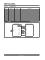
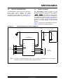
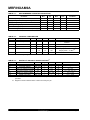
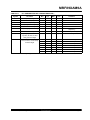
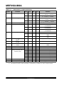
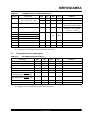
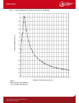
MRF89XAM9A
TABLE 4-6:
Symbol
RFOP
TRANSMITTER AC CHARACTERISTICS(1)
Description
Min
Typ
Max
Unit
Condition
RF Output Power, Programmable
with 8 Steps of typ. 3 dB
—
+12.5
—
dBm
Maximum power setting
—
-8.5
—
dBm
Minimum power setting
Phase Noise
—
-112
—
dBc/Hz
Measured with a 600 kHz
offset at the transmitter output
Transmitted Spurious
—
—
-47
dBc
At any offset between 200 kHz
and 600 kHz, unmodulated
carrier, fdev = 50 kHz
PN
TXSP
Tx2
No modulation, see Note(2)
Second Harmonic
Tx3
Third Harmonic
Tx4
Fourth Harmonic
Txn
Harmonics above Tx4
—
—
-40
dBm
FSKDEV
FSK Deviation
±33
±55
±200
kHz
Programmable
TSTWF
Transmitter Wake-up Time
—
120
500
µs
From FS to Tx ready
Transmitter Wake-up Time
—
600
900
µs
From Stand-by to Tx ready
TSTWS
Note 1:
2:
4.1
Guaranteed by design and characterization.
Transmitter in-circuit performance with SAW filter and crystal.
Timing Specification and Diagram
TABLE 4-7:
SPI TIMING SPECIFICATION(1,2)
Parameter
Min
Typ
Max
Unit
Condition
SPI Configure Clock Frequency
—
—
6
MHz
—
SPI Data Clock Frequency
—
—
1
MHz
—
Data Hold and Setup Time
2
—
—
µs
—
SDI Setup Time for SPI Configure
250
—
—
ns
—
SDI Setup Time for SPI Data
312
—
—
ns
—
CSCON Low to SCK Rising Edge;
SCK Falling Edge to CSCON High
500
—
—
ns
—
CSDATA Low to SCK Rising Edge;
SCK Falling Edge to CSDATA High
625
—
—
ns
—
CSCON Rising to Falling Edge
500
—
—
ns
—
CSDATA Rising to Falling Edge
625
—
—
ns
—
Note 1:
2:
Typical Values: TA = 25°C, VIN = 3.3V, Crystal Frequency = 12.8 MHz, unless otherwise specified.
Negative current is defined as the current sourced by the pin.
© 2011 Microchip Technology Inc.
Preliminary
DS75017A-page 25