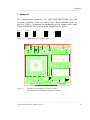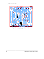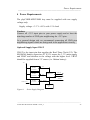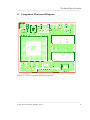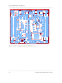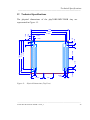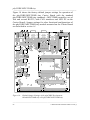
1
phyCORE-MPC5200B
tiny
Hardware Manual
Edition September 2007
A product of a PHYTEC Technology Holding company
phyCORE-MPC5200B tiny
___________________________________________________________
In this manual are descriptions for copyrighted products that are not explicitly
indicated as such. The absence of the trademark (™) and copyright (©) symbols
does not imply that a product is not protected. Additionally, registered patents and
trademarks are similarly not expressly indicated in this manual.
The information in this document has been carefully checked and is believed to be
entirely reliable. However, PHYTEC Messtechnik GmbH assumes no
responsibility for any inaccuracies. PHYTEC Messtechnik GmbH neither gives
any guarantee nor accepts any liability whatsoever for consequential damages
resulting from the use of this manual or its associated product. PHYTEC
Messtechnik GmbH reserves the right to alter the information contained herein
without prior notification and accepts no responsibility for any damages which
might result.
Additionally, PHYTEC Messtechnik GmbH offers no guarantee nor accepts any
liability for damages arising from the improper usage or improper installation of
the hardware or software. PHYTEC Messtechnik GmbH further reserves the right
to alter the layout and/or design of the hardware without prior notification and
accepts no liability for doing so.
© Copyright 2007 PHYTEC Messtechnik GmbH, D-55129 Mainz.
Rights - including those of translation, reprint, broadcast, photomechanical or
similar reproduction and storage or processing in computer systems, in whole or
in part - are reserved. No reproduction may occur without the express written
consent from PHYTEC Messtechnik GmbH.
Address:
EUROPE
NORTH AMERICA
PHYTEC Technologie Holding AG
Robert-Koch-Str. 39
D-55129 Mainz
GERMANY
PHYTEC America LLC
203 Parfitt Way SW, Suite G100
Bainbridge Island, WA 98110
USA
Ordering
+49 (800) 0749832
Information: [email protected]
1 (800) 278-9913
[email protected]
Technical
Support:
+49 (6131) 9221-31
[email protected]
1 (800) 278-9913
[email protected]
Fax:
+49 (6131) 9221-33
1 (206) 780-9135
Web Site:
http://www.phytec.de
http://www.phytec.com
3nd Edition September 2007
____________________________________________________________________________________
© PHYTEC Messtechnik GmbH L-678e_3
Contents
___________________________________________________________
Preface........................................................................................................... 1
1
Introduction ......................................................................................... 3
1.1 Block Diagram ............................................................................. 6
1.2 View of the phyCORE-MPC5200B tiny...................................... 7
1.3 Minimum Requirements to Operate the phyCORE-MPC5200B
tiny................................................................................................ 8
2
Pin Description .................................................................................... 9
3
Jumpers ..............................................................................................19
4
Power Requirements.........................................................................23
4.1 Voltage Supervision and Reset ..................................................24
5
System Start-Up Configuration .......................................................25
6
System Memory.................................................................................27
6.1 Flash Memory ............................................................................28
6.2 DDR SDRAM ............................................................................30
6.3 Serial Memory............................................................................31
7
Real-Time Clock RTC-8564 (U5) ....................................................33
8
Serial Interfaces.................................................................................35
8.1 RS-232 Interface ........................................................................35
8.2 Ethernet Interface .......................................................................36
8.2.1 PHY Physical Layer Transceiver .................................. 36
8.2.2 MAC Address................................................................37
8.3 USB 1.1 Host Interface ..............................................................38
9
The U-Boot Boot Loader ..................................................................39
9.1 U-Boot Default System Configuration....................................... 40
9.2 System Resources Required by U-Boot ..................................... 41
9.2.1 The "Backup" U-Boot ...................................................41
9.3 Modifying the U-Boot Loader....................................................44
10 JTAG Interface..................................................................................45
11 Component Placement Diagram......................................................47
12 Technical Specifications....................................................................49
13 Hints for Handling the Module........................................................53
14 The phyCORE-MPC5200B tiny on the Carrier Board................. 55
14.1 Concept of the Carrier Board phyCORE-MPC5200B ............... 55
14.2 Carrier Board phyCORE-MPC5200B tiny Connectors and
Jumpers.......................................................................................57
14.2.1 Connectors.....................................................................57
14.2.2 Jumpers on the Carrier Board phyCORE-MPC5200B
tiny.................................................................................60
14.3 Functional Components on the phyCORE-MPC5200B tiny
Carrier Board..............................................................................63
14.3.1 Power Supply at X6 ......................................................63
___________________________________________________________________________________
© PHYTEC Messtechnik GmbH L-678e_3
phyCORE-MPC5200B tiny
___________________________________________________________
14.3.2 First Serial Interface at Socket P3A.............................. 64
14.3.3 Second Serial Interface at Socket P3B ......................... 65
14.3.4 First CAN Interface at Plug P2A .................................. 66
14.3.5 Second CAN Interface at Plug P2B.............................. 68
14.3.6 Programmable LED D16 .............................................. 70
14.3.7 Ethernet Interface P1A.................................................. 71
14.3.8 USB Host Interface P1B ............................................... 72
14.3.9 Audio Interface ............................................................. 73
14.3.10 Compact Flash Card Socket X10.................................. 74
14.3.11 IDE Interface X11......................................................... 74
14.3.12 PCI Card Slot X4 .......................................................... 75
14.3.13 Misc. Configuration Jumpers on the Carrier Board...... 76
14.3.14 FPGA JTAG Connector X8 .......................................... 76
14.3.15 Pin Assignment Summary of the phyCORE, the
Expansion Bus and the Patch Field............................... 77
14.3.16 Gold CAP Connector C119 .......................................... 95
Index ........................................................................................................... 96
A Appendix............................................................................................ 98
A.1 Release Notes............................................................................. 98
____________________________________________________________________________________
© PHYTEC Messtechnik GmbH L-678e_3
Contents
___________________________________________________________
Index of Figures and Tables
Figure 1:
Block Diagram phyCORE-MPC5200B tiny.............................. 6
Figure 2:
Top-View of the phyCORE-MPC5200B tiny PCB Rev. 1245.27
Figure 3:
Bottom-View of the phyCORE-MPC5200B tiny PCB Rev.
1245.2......................................................................................... 7
Figure 4:
Pinout of 0the phyCORE-MPC5200B tiny (Bottom View) .... 10
Figure 5:
Numbering of the Jumper Pads................................................ 19
Figure 6:
Location of the Jumpers (Controller Side) (phyCOREMPC5200B tiny Standard Version) ......................................... 19
Figure 7 Location of the Jumpers (Bottom Side) (phyCORE-MPC5200B
tiny Standard Version) ............................................................. 20
Figure 8:
Power Supply Diagram ............................................................ 23
Figure 9:
Serial Memory I2C Slave Address ........................................... 32
Figure 10: U-Boot Memory Map............................................................... 43
Figure 11: 1245.2 component placement Top view .................................... 47
Figure 12:1245.2 component placement Bottom view................................ 48
Figure 13: Physical Dimensions (Top View) ............................................ 49
Figure 14: Modular Development and Expansion Board Concept with the
phyCORE-MPC5200B tiny ..................................................... 56
Figure 15: Location of Connectors on the phyCORE-MPC-5200B-tiny
Carrier Board............................................................................ 58
Figure 16: Numbering of Jumper Pads...................................................... 60
Figure 17: Location of the Jumpers (View of the Component Side) ........ 61
Figure 18: Default Jumper Settings of the phyCORE Development Board
MPC5200B tiny with phyCORE-MPC5200B tiny.................. 62
Figure 19: Connecting the Supply Voltage at X6...................................... 63
Figure 20: Pin Assignment of the DB-9 Socket P3A as RS-232 (PSC3)
(Front View)............................................................................. 64
Figure 21: Pin Assignment of the DB-9 Socket P3B as Second RS-232
(Front View)............................................................................. 65
___________________________________________________________________________________
© PHYTEC Messtechnik GmbH L-678e_3
phyCORE-MPC5200B tiny
___________________________________________________________
Figure 22: Pin Assignment of the DB-9 Plug P2A (CAN Transceiver on
Carrier Board) .......................................................................... 66
Figure 23: Pin Assignment of the DB-9 Plug P2B (CAN Transceiver on
Carrier Board) .......................................................................... 68
Figure 24: Pin Assignment Scheme of the Expansion Bus....................... 78
Figure 25: Pin Assignment Scheme of the Patch Field............................. 78
Table 1:
Default Port Configuration ........................................................ 9
Table 2:
Pinout of the phyCORE-Connector X1 ................................... 18
Table 3:
Jumper Settings........................................................................ 22
Table 4:
System Start-Up Configuration ............................................... 26
Table 5:
Choice of Flash Memory Devices and Manufacturers ............ 28
Table 6:
DDR SDRAM Device Selection.............................................. 30
Table 7:
Serial Memory Options for U4 ................................................ 31
Table 8:
Serial Memory I2C Address (Examples) ................................. 32
Table 9:
Signal Definition PHY Ethernet Port (U2).............................. 37
Table 10:
JTAG Interface ........................................................................ 45
Table 11:
Technical Data ......................................................................... 50
Table 12:
Jumper Configuration for the First RS-232 Interface.............. 64
Table 13:
Jumper Configuration of the DB-9 Socket P3B (PSC6) ......... 65
Table 14:
Jumper Configuration for CAN Plug P2A using the CAN
Transceiver on the Carrier Board............................................. 66
Table 15:
Improper Jumper Settings for the CAN Plug P2A (CAN
Transceiver on the Carrier Board) ........................................... 67
Table 16:
Jumper Configuration for CAN Plug P2B using the CAN
Transceiver on the Carrier Board............................................ 68
Table 17:
Improper Jumper Settings for the CAN Plug P2B (CAN
Transceiver on the Carrier Board) ........................................... 69
Table 18:
JP17 Configuration of the Programmable LED D3................ 70
Table 19:
JP8, JP9 Ethernet Interface Configuration.............................. 71
Table 20:
JP2 USB Host Interface Configuration................................... 72
____________________________________________________________________________________
© PHYTEC Messtechnik GmbH L-678e_3
Contents
___________________________________________________________
Table 21:
JP14, JP15 AC97 Audio Interface Configuration................... 73
Table 22:
J3, JP11 CF Card Interface Configuration .............................. 74
Table 23:
Misc. Configuration Jumpers JP3, JP10, JP12 ........................ 76
Table 24:
FPGA JTAG Connector X8 Pin Assignment........................... 76
Table 25:
Pin Assignment Data/Address Bus for the phyCOREMPC5200B tiny / Carrier Board / Expansion Board ............... 80
Table 26:
Pin Assignment Dedicated LocalPlus Control Signals
phyCORE-MPC5200B tiny / Carrier Board / Expansion Board81
Table 27:
Pin Assignment PCI dedicated signals phyCORE-MPC5200B
tiny / Carrier Board / Expansion Board ................................... 82
Table 28:
Pin Assignment Dedicated ATA /IDE Interface Signals
phyCORE-MPC5200B tiny / Carrier Board / Expansion Board83
Table 29:
Pin Assignment Interfaces for the phyCORE-MPC5200B tiny /
Carrier Board / Expansion Board............................................. 85
Table 30:
Pin Assignment COP Interface Signals for the phyCOREMPC5200B tiny /Carrier Board / Expansion Board ................ 85
Table 31:
Pin Assignment Misc. Control Signals for the phyCOREMPC5200B tiny /Carrier Board / Expansion Board ................ 87
Table 32:
Pin Assignment FPGA Signals for the phyCORE-MPC5200B
tiny /Carrier Board / Expansion Board .................................... 91
Table 33:
Pin Assignment Power Supply for the phyCORE-MPC5200B
tiny / Carrier Board / Expansion Board ................................... 93
Table 34:
Unused Pins on the phyCORE-MPC5200B tiny / Carrier Board
/ Expansion Board .................................................................... 95
___________________________________________________________________________________
© PHYTEC Messtechnik GmbH L-678e_3
Preface
___________________________________________________________
Preface
This phyCORE-MPC5200B tiny Hardware Manual describes the
board’s design and functions. Precise specifications for the Freescale
MPC5200B microcontroller series can be found in the enclosed
MPC5200B microcontroller Data Sheet/User's Manual. If software is
included please also refer to additional documentation for this
software.
In this hardware manual and in the attached schematics, low active
signals are denoted by a "/" in front of the signal name (i.e.: /RD). A
"0" indicates a logic-zero or low-level signal, while a "1" represents a
logic-one or high-level signal.
Declaration regarding Electro Magnetic Conformity
of the PHYTEC phyCORE-MPC5200B tiny
PHYTEC Single Board Computers (henceforth products) are designed
for installation in electrical appliances or as dedicated Evaluation
Boards (i.e.: for use as a test and prototype platform for
hardware/software development) in laboratory environments.
Note:
PHYTEC products lacking protective enclosures are subject to
damage by ESD and, hence, may only be unpacked, handled or
operated in environments in which sufficient precautionary measures
have been taken in respect to ESD dangers. It is also necessary that
only appropriately trained personnel (such as electricians, technicians
and engineers) handle and/or operate these products. Moreover,
PHYTEC products should not be operated without protection circuitry
if connections to the product’s pin header rows are longer than 3 m.
___________________________________________________________________________________
© PHYTEC Messtechnik GmbH L-678e_3
1
phyCORE-MPC5200B tiny
___________________________________________________________
PHYTEC products fulfill the norms of the European Union's Directive
for Electro Magnetic Conformity only in accordance to the
descriptions and rules of usage indicated in this hardware manual
(particularly in respect to the pin header rows or connectors, power
connector and serial interface to a host-PC).
Implementation of PHYTEC products into target devices, as well as
user modifications and extensions of PHYTEC products, is subject to
renewed establishment of conformity to, and certification of, Electro
Magnetic Directives. Users should ensure conformance following any
modifications to the products as well as implementation of the
products into target systems.
The phyCORE-MPC5200B tiny is one of a series of PHYTEC Single
Board Computers that can be populated with different controllers and,
hence, offers various functions and configurations. PHYTEC supports
common 8-, 16- and numerous 32-bit controllers on two types of
Single Boards Computers:
(1) as the basis for Rapid Development Kits which serve as a
reference and evaluation platform
(2) as insert-ready, fully functional phyCORE OEM modules, which
can be embedded directly into the user’s target design.
PHYTEC's microcontroller modules allow engineers to shorten
development horizons, reduce design costs and speed project concepts
from design to market.
____________________________________________________________________________________
2
© PHYTEC Messtechnik GmbH L-678e_3
Introduction
___________________________________________________________
1 Introduction
The phyCORE-MPC5200B tiny belongs to PHYTEC's phyCORE
Single Board Computer module family. The phyCORE SBCs
represent the continuous development of PHYTEC Single Board
Computer technology. Like its mini-, micro- and nanoMODUL
predecessors, the phyCORE boards integrate all core elements of a
microcontroller system on a sub-miniature board and are designed in a
manner that ensures their easy expansion and embedding in peripheral
hardware developments.
As independent research indicates that approximately 70 % of all EMI
(Electro Magnetic Interference) problems stem from insufficient
supply voltage grounding of electronic components in high frequency
environments the phyCORE board design features an increased pin
package. The increased pin package allows dedication of
approximately 20 % of all pin header connectors on the phyCORE
boards to Ground. This improves EMI and EMC characteristics and
makes it easier to design complex applications meeting EMI and EMC
guidelines using phyCORE boards even in high noise environments.
phyCORE boards achieve their small size through modern SMD
technology and multi-layer design. In accordance with the complexity
of the module, 0402-packaged SMD and laser-drilled Microvias
components are used on the boards, providing phyCORE users with
access to this cutting edge miniaturization technology for integration
into their own design.
The phyCORE-MPC5200B tiny is a subminiature (53 x 57 mm)
insert-ready Single Board Computer populated with Freescale’s
PowerPC MPC5200B microcontroller. Its universal design enables its
insertion in a wide range of embedded applications. All controller
signals and ports extend from the controller to high-density
(0.635 mm) Molex pin header connectors aligning two sides of the
board, allowing it to be plugged like a "big chip" into a target
application.
___________________________________________________________________________________
© PHYTEC Messtechnik GmbH L-678e_3
3
phyCORE-MPC5200B tiny
___________________________________________________________
Precise specifications for the controller populating the board can be
found in the applicable controller User's Manual or Data Sheet. The
descriptions in this manual are based on the MPC5200B controller. No
description of compatible microcontroller derivative functions is
included, as such functions are not relevant for the basic functioning
of the phyCORE-MPC5200B tiny.
The phyCORE-MPC5200B tiny offers the following features:
• Single Board Computer in subminiature form factor (53 x 57 mm)
according to phyCORE specifications
• all applicable controller and other logic signals extend to two
high-density 100-pin Molex connectors
• processor: Freescale embedded PowerPC MPC5200B
• single 3.3 V (max. 1.2 A) supply voltage
Internal Features of the MPC5200B:
• e300 core
760 MIPS at 400 MHz (-40 to +85 °C)
16 k instruction cache, 16 k data cache
Double precision FPU
Instruction and data MMU
• SDRAM / DDR SDRAM memory Interface
up to 132 MHz operation
SDRAM and DDR SDRAM support
256 MByte addressing range per CS, two CS available
• Flexible multi-function external bus interface
• Peripheral component interconnect (PCI) controller
• ATA controller
• BestComm DMA subsystem
• 6 programmable serial controllers (PSC), configurable for the
following functions:
____________________________________________________________________________________
4
© PHYTEC Messtechnik GmbH L-678e_3
Introduction
___________________________________________________________
• Fast Ethernet controller (FEC)
Supports 100Mbps IEEE 802.3 MII, 10 Mbps IEEE 802.3 MII
• Universal serial bus controller (USB)
USB revision 1.1 host
• Two inter-integrated circuit interfaces (I²C)
• Serial peripheral interface (SPI)
• Dual CAN 2.0 A/B controller (MSCAN)
• J1850 byte data link controller (BDLC)
• Test/debug features
• JTAG (IEEE 1149.1 test access port)
• Common on-chip processor (COP) debug port
Memory Configuration1 :
• DDR SDRAM: 64 MByte to 128 MByte
• Flash: 16 MByte to 32 MByte Intel Strata Flash memory, 16-bit
memory width, only asynchronous devices are supported
• I²C memory: 4 kByte EEPROM
Other Board-Level Features:
• Two UART ports, RS-232 interfaces (RxD/TxD)
• One 10/100Mbit Ethernet port via optional Micrel PHY
• I²C Real-Time Clock with calendar and alarm function
• Optional industrial temperature range (-40…+85°C)
1:
Please contact PHYTEC for more information about additional module configurations.
___________________________________________________________________________________
© PHYTEC Messtechnik GmbH L-678e_3
5
phyCORE-MPC5200B tiny
___________________________________________________________
1.1 Block Diagram
MPC5200B
64 to 128MB
DDR-SDRAM
133MHz
32-bit
DDR SDRAM Bus
LoCalPlus-Bus:
External Bus Interface
PCI Bus V2.2 (33/66MHz)
ATA Interface
LocalPlus Bus
MPC603e
series e300
core
16 to 32MB
FLASHEEPROM
16-bit
16k D-cache
33 MHz Quarz
396 MHz core Clock
16k I-cache
2
2
I C-Memory
EEPROM
4KByte
FPU
Floating Point
Unit
I2C 1
MMU
Memor Management
Unit
I2C 0
DMA
BestCom I/OSubsystem
JTAG port for re-programming
FEC FastEthernet
I C-RTC
Clock
Calendar
Alarm
Ethernet PHY
USB Host
PSC1 (AC97)
PSC2 (CAN1/2)
RS232 Transceiver
PS3 (UART + SPI)
PSC 6 (UART)
RS232 Transceiver
p
h
y
C
O
R
E
C
o
n
n
e
c
t
o
r
/IRQRTC
I 2C-Bus 1
2
I C-Bus 0
10/100 Mbit Ethernet
USB 1.1 Host Interface
PSC1 could be used as AC97 codec
CAN0 TTL
CAN1 TTL
UART3 RXD3 / TXD3
UART3 TTL
SPI Bus
UART0 RXD6 / TXD6
UART6 TTL
Timer
ATA_CS
Timer Outputs (PWM)
/CS-Signals for ATA-Interface
COP/JTAG
COP/JTAG Debug-/Test Port
+1V5
+2V5
+3V3
Figure 1:
Power
Supply
VBat +3V for RTC and SRAM
Power +3V3@1,2A
Block Diagram phyCORE-MPC5200B tiny
____________________________________________________________________________________
6
© PHYTEC Messtechnik GmbH L-678e_3
Introduction
___________________________________________________________
1.2 View of the phyCORE-MPC5200B tiny
R73
RN6
R10
C57 C9
CB301
R31
R29
R28
U8
C58 C59
X2
R52
R4
U14
R74
CB206
U5
J7
R26 R27 R5
Top-View of the phyCORE-MPC5200B tiny PCB Rev. 1245.2
TP3 TP4
C41
C29
C40
C13
R2
R25
R3
C12
CB311
C11
U12
J4
J5
RN3
15
CB102
CB100
C47
C35
C16
CB108 CB302
C46
CB304
CB104
R65 C50 C49
CB107
RN21
CB203
CB308 CB105
R7
C36
R79
C48
C17
CB303
CB202
C51
CB205
R77
U6
J3 R68
R24
XT1
CB103
R63
C39
R35
R36
U2
R17R18
R58
R47
R19
TP5
CB204
L7
L3
R51
C28 C24
R78
R84
C1
U3
R14 R13
R15 R16
J8 J9
R12
C2
C10
R75
R76
J1
C6
C4
C5
C3
X1
L1
C14
CB312 C15
C44
C19 CB106
R38 U10
CB309
R11
R57
C45
C25
J2
C34
CB101
L2
CB201
C22
U9
R49
R50
R46
CB200
R6 R64
R48
C27
R37
C33
C18
CB310
Figure 3:
C56
U4
RN15 RN14 RN19 RN11 RN12 RN8
Figure 2:
R30
R55
R56
R23
C53
C52
CB313
R72
CB305
R71
U13
U15
U16
RN4
U7
J6
R22 R53
D7
C54 C55 R33 C7
RN18 RN17 RN16 RN13 RN10 RN9
U1
D8
R1
R9
R21
CB306
RN7
U17
C30
U11
R44 R54 R59 R32 CB207
CB314
C26
TP1
RN5
R39
CB300
C31
R81 R80
R40
D5
R34
R60 R61
R8
CB307
R43 R42
R41 R20
C38 R62
D4
R83
XT3
C21
C20
TP6
XT2
C32
D6
CB208
R45 C37
TP7
R67
R69
R70
1 R82
R66
RN2
Bottom-View of the phyCORE-MPC5200B tiny PCB Rev. 1245.2
___________________________________________________________________________________
© PHYTEC Messtechnik GmbH L-678e_3
7
phyCORE-MPC5200B tiny
___________________________________________________________
1.3 Minimum Requirements to Operate the
phyCORE-MPC5200B tiny
Basic operation of the phyCORE-MPC5200B tiny only requires
supply of a +3V3 input voltage and the corresponding GND
connection.
These supply pins are located at the phyCORE-connector X1:
+3V3
GND
X1
X1
1C, 2C, 4C, 5C, 1D, 2D
3C, 3D, 7C, 9D, 12C, 14D
Caution:
We recommend connecting all available +3V3 input pins to the power
supply system on a custom carrier board housing the
phyCORE-MPC5200B tiny and at least the matching number of GND
pins neighboring the +3 V3 pins.
In addition, proper implementation of the phyCORE module into a
target application also requires connecting all GND pins neighboring
signals that are being used in the application circuitry.
Please refer to section 4 for more information.
____________________________________________________________________________________
8
© PHYTEC Messtechnik GmbH L-678e_3
Pin Description
___________________________________________________________
2 Pin Description
Please note that all module connections are not to exceed their
expressed maximum voltage or current. Maximum signal input values
are indicated in the corresponding controller manuals/data sheets. As
damage from improper connections varies according to use and
application, it is the user's responsibility to take appropriate safety
measures to ensure that the module connections are protected from
overloading through connected peripherals.
Many of the phyCORE-MPC5200B tiny pins offer alternative
functions. These alternative functions must be activated by
configuring the applicable controller registers prior to their use.
Certain controller functions are pre-configured based on the module’s
design and are shown in Table 1. Signals that are routed directly from
the CPU to the Molex connectors can configured to any available
alternative function desired by the user. In contrast, signals that are
used on the phyCORE-MPC5200 tiny as listed in Table 1 can only be
used if a special module configuration was purchased (e.g. SBC
version without on-board RS-232 transceivers. Please contact
PHYTEC for more details.
Note:
The following sections of this manual assume use of the port pins
according to configuration listed in Table 1.
CPU
Port
PSC1
PSC2
PSC3
USB
Ethernet
Timer
I2C
PSC6
Table 1:
Function
AC97_1
CAN 1/2
UART3/SPI
USB
Ethernet w/ MD
ATA_CS
I2C1 / I2C2
UART6
Port_conf
Register Bits
01x [29:31]
001 [25:27]
1100 [20:23]
01 [18:19]
0101 [12:15]
00_11 [2:3_6:7]
default
101 [9:11]
Used on
phyCORE SBC
No
No
Yes
No
Yes
No
Yes (I2C1 available)
Yes
Default Port Configuration
___________________________________________________________________________________
© PHYTEC Messtechnik GmbH L-678e_3
9
phyCORE-MPC5200B tiny
___________________________________________________________
As Figure 4 indicates, all controller signals extend to surface mount
technology (SMT) connectors (0.635 mm) lining two sides of the
module (referred to as phyCORE-connector; refer to section 2). This
allows the phyCORE-MPC5200B tiny to be plugged into any target
application like a "big chip".
/
D C
B A
50
X1
Figure 4:
1
1
1
1
50
50
X1
Pinout of 0the phyCORE-MPC5200B tiny (Bottom View)
Table 2 provides an overview of the pinout of the phyCOREconnector.
Please refer to the Freescale MPC5200B User Manual/Data Sheet for
details on the functions and features of controller signals and port
pins.
____________________________________________________________________________________
10
© PHYTEC Messtechnik GmbH L-678e_3
Pin Description
___________________________________________________________
Pin Number
Pin Row X1A
1A
2A, 7A, 12A,
17A, 22A, 27A,
32A, 37A, 42A,
47A
3A
4A
Signal
I/O
Comments
NC
GND
-
Not connected
Ground 0 V
/IRQ3
/IRQ0
I
I
Interrupt input 3 of the processor.
Interrupt input 0 of the processor.
LocalPlus Bus control signals
Chip Select 1
Address Latch Enable
Read, not Write
Transfer Start
Chip Select 4
Chip Select 6 (PSC3 is UART3)
LocalPlus Address/Data Signals
5A
6A
8A
29A
30A
31A
/LP_CS1
/LP_ALE
/LP_RD#WR
/LP_Ts
/LP_Cs4
/LP_Cs6
9A
10A
11A
13A
14A
15A
16A
18A
19A
20A
21A
23A
24A
25A
26A
28A
33A
EXT_AD1
EXT_AD2
EXT_AD4
EXT_AD7
EXT_AD9
EXT_AD10
EXT_AD12
EXT_AD15
EXT_AD17
EXT_AD18
EXT_AD20
EXT_AD23
EXT_AD25
EXT_AD26
EXT_AD28
EXT_AD31
ETH_TXD3
34A
35A
36A
38A
39A
ATA_CS_0
ATA_CS_1
ATA_IOCHRDY
/ATA_IOR
ATA_INTRQ
O
O
O
O
O
O
I/O
O
O
O
O
I
Already used by the MII interface between
CPU and Ethernet PHY. Could be used as
J1850_TX signal, if the PHY is not populated
or in "isolation mode".
The pin state is latched by the CPU after reset
and used as "byte lane swap" configuration.
Refer to section 5, "System Start-Up
Configuration". There is a 10kOhm pulldown resistor on this signal..
ATA Interface Signals
Timer Port configured as ATA_CS (Timer0)
Timer Port configured as ATA_CS (Timer1)
ATA negated to extend transfer
ATA read
ATA interrupt request
___________________________________________________________________________________
© PHYTEC Messtechnik GmbH L-678e_3
11
phyCORE-MPC5200B tiny
___________________________________________________________
Pin Number
40A
41A
43A
44A
45A
46A
48A
49A
50A
Signal
/PCI_RESET
/PCI_GNT
/PCI_CBE_3
/PCI_CBE_2
/PCI_IRDY
/PCI_DEVSEL
/PCI_PERR
/PCI_SERR
/PCI_CBE_1
I/O
O
O
O
O
O
O
O
O
O
Comments
Dedicated PCI Signals
Reset output (open drain)
Bus grant
Command byte enable 3
Command byte enable 2
Initiator (HOST) ready
Device select
Parity error
System Error (open drain)
Command byte enable 1
____________________________________________________________________________________
12
© PHYTEC Messtechnik GmbH L-678e_3
Pin Description
___________________________________________________________
Pin Number
Pin Row X1B
1B
2B
3B
4B, 9B, 14B,
19B, 24B, 29B,
34B, 39B, 41B,
44B, 49B
Signal
I/O Comments
RTC_CLKOUT
/IRQ1
/IRQ2
GND
O
I
I
5B
6B
7B
28B
30B
31B
/LP_CS2
/LP_CS3
/LP_Oe
LP_Ack
/LP_CS5
/LP_CS7
O
O
O
8B
10B
11B
12B
13B
15B
16B
17B
18B
20B
21B
22B
23B
25B
26B
27B
32B
EXT_AD0
EXT_AD3
EXT_AD5
EXT_AD6
EXT_AD8
EXT_AD11
EXT_AD13
EXT_AD14
EXT_AD16
EXT_AD19
EXT_AD21
EXT_AD22
EXT_AD24
EXT_AD27
EXT_AD29
EXT_AD30
Test_Sel_1
I/O
33B
ETH_RXD1
I
35B
36B
37B
38B
ATA_DRQ
/ATA_IOW
ATA_Isolation
/ATA_DACK
I
O
O
O
O
O
I/O
Clock output of the I²C RTC U5
Interrupt input 1 of the processor
Interrupt input 2 of the processor
Ground 0 V
LocalPlus Bus Signals
Chip Select 2
Chip Select 3
Output Enable
Acknowledge
Chip Select 5
Chip Select 7 (PSC3 is UART3)
LocalPlus Address/Data Signals
Input in CPU production test. Can be
configured as LocalPlus-Bus TSIZ bit Refer to
section 7.3.2.1.1 in the MPC5200 controller
User’s Manual.
Already used by the MII interface between
CPU and Ethernet PHY. Can be used as
J1850_RX signal, if the PHY is not populated
or in "isolation mode".
ATA Interface Signals
ATA DMA request
ATA write
ATA write enable for PCI bus sharing
ATA DMA acknowledge
___________________________________________________________________________________
© PHYTEC Messtechnik GmbH L-678e_3
13
phyCORE-MPC5200B tiny
___________________________________________________________
Pin Number
40B
42B
43B
45B
46B
47B
48B
50B
Signal
PCI_CLOCK
/PCI_REQ
PCI_IDSEL
/PCI_FRAME
/PCI_TRDY
/PCI_STOP
PCI_PAR
/PCI_CBE_0
I/O Comments
O
O
O
O
I
O
O
O
Dedicated PCI Signals
PCI and external peripheral clock
PCI bus request
Initial device select
Frame start
Target ready
Transition stop
Bus parity
Command byte enable 0
____________________________________________________________________________________
14
© PHYTEC Messtechnik GmbH L-678e_3
Pin Description
___________________________________________________________
Pin Number Signal
Pin Row X1C
I/O
1C, 2C, 4C, 5C +3V3
3C, 7C, 12C, GND
17C, 22C, 27C,
32C, 37C, 42C,
47C
6C
VBAT
I
-
Supply voltage +3.3 VDC
Ground 0 V
I
Connection for external battery (+) 2.4 - 3.3 V
to supply (backup) the RTC U5
Already used by the MII-Interface between
CPU and Ethernet PHY. The pin state is
latched by the CPU after reset and used as
"boot high" configuration. Refer to section 5
"System Start-Up Configuration". A 10kOhm
pull-up resistor is connected to this signal.
Dedicated GPIO with wakeup capability
Note: This is a 2.5V based GPIO!!!
External SRESET is an open drain signal
which is connected to a 10 kOhm pull-up
resistor on the module. Assertion of SRESET
causes assertion of the internal soft reset.
Internal soft reset is actually an interrupt that
takes the same exception vector as HRESET.
In particular, this means that SRESET cannot
abort a hung XLB operation, and no device
should use SRESET in a way that interferes
with any bus operation in progress.
SRESET can also be asserted by internal
sources. When SRESET is asserted internally,
external SRESET is also asserted.
HRESET is a bi-directional signal with a
Schmitt-trigger input and an open drain output.
The HRESET signal is connected a 10 kOhm
pull-up resistor on the module. Assertion of
external HRESET causes external HRESET
and SRESET as well as internal hard and soft
resets to be asserted for at least 4096 reference
clock cycles. During PORRESET or HRESET
the reset configuration word is sampled to
establish the initial state of various vital
internal MPC5200B functions. The reset
configuration word is latched internally when
PORRESET or HRESET is released.
AC97 Codec Signals (PSC1)
Reset signal to the external AC97 device
Frame sync, or start-of-frame (SOF)
Driven by the external serial bit-clock
Receiver serial data input
CAN transmit output of the second CAN
interface (PSC2)
PSC6 receive data signal
PSC6 transmit data signal
8C
ETH_TXD1
O
9C
GPIO_WKUP_6
I/O
10C
/SRESET
I/O
11C
/HRESET
I/O
13C
14C
15C
16C
18C
AC97_1_RES
AC97_1_SYNC
AC97_1_BITCLK
AC97_1_SDATA_IN
CAN2_TX
O
O
I
I
O
19C
20C
UART6_RXD_TTL
UART6_TXD_TTL
I
O
Comments
___________________________________________________________________________________
© PHYTEC Messtechnik GmbH L-678e_3
15
phyCORE-MPC5200B tiny
___________________________________________________________
Pin Number Signal
I/O
21C
RXD6_232
I
23C
TXD6_232
O
24C
25C
/UART6_RTS_TTL
/UART6_CTS_TTL
I
O
26C
28C
29C
30C
31C
I2C2_CLK
I2C2_IO
Timer4
Timer5
I2C1_CLK
33C
34C
35C
36C
38C
41C
ETH_LINK
ETH_SPEED
ETH_RXETH_TX/ETH_PD
ET_NWAYEN
O
O
I
O
I
O
39C
/COP_TRST
I
40C
43C
44C
CK_STOP
PSC2_4
Timer6
45C
46C
48C
49C
50C
USB1_OVRCRNT
USB1_SUSPEND
USB1_RXN
USB1_TXN
/USB1_OE
I/O
I/O
I/O
I/O
I/O
O
I/O
I/O
I
O
I
O
O
Comments
RxD input on the RS-232 transceiver for the
MPC UART (PSC6)
TxD output on the RS-232 transceiver for the
MPC UART (PSC6)
PSC6 request to send signal
PCS6 clear to send signal
Second I²C Interface
Clock (SCL)
Data (SDA)
Timer 4 signal of the MPC5200B
Timer 5 signal of the MPC5200B
Clock for first I2C-Interface (SCL)
10/100MBit TP Ethernet Interface (if onboard PHY is not populated, pins are NC)
Link/Activity LED (L=link; toggle=act)
Speed LED (H=10 Mbit/s, L=100 Mbit/s)
Differential receive input
Differential transmit output
Power down
Collision LED (H = no collision)
JTAG Interface
JTAG reset input. Via logic OR connected to
/PORRESET resulting in /CPU_TRST signal.
Scan enable, clock stop
Freely available GPIO with wakeup function
Timer 6 signal of the MPC5200B
USB1 (Host)
Over current
Suspend
Receive negative
Transmit negative
Output enable
____________________________________________________________________________________
16
© PHYTEC Messtechnik GmbH L-678e_3
Pin Description
___________________________________________________________
Pin Number Signal
Pin Row X1D
I/O
Comments
1D, 2D
3D, 9D, 14D,
19D, 24D, 29D,
34D, 39D, 44D,
49D
4D, 5D
6D
+3V3
GND
I
-
Supply voltage +3.3 VDC
Ground 0 V
NC
VCC_SRAM
O
7D
8D
RESOUT
/PHYReset
O
I
10D
/RESIN
I
11D
12D
13D
GPIO_WKUP_7
Timer2
Timer3
15D
16D
17D
18D
AC97_SDATA_OUT
UART3_RXD_TTL
UART3_TXD_TTL
CAN2_RX
O
I
O
I
20D
21D
CAN1_RX
CAN1_TX
I
O
Not connected
VCC_SRAM supply voltage is generated by
VBAT or +3V3 using a battery backup circuit
(MAX6364). VCC_SRAM serves as supply
voltage for the Real-Time Clock.
Reset output of the voltage supervisor circuit
A low on this pin forces only the PHY into
reset state
Reset input signal of the MPC5200B tiny. It
could be asserted via connection to a reset push
button. Signal connected to +3V3 via 10 kOhm
pull-up resistor.
Dedicated GPIO with wakeup capability
Timer 2 signal of the MPC5200
Timer 3 signal of the MPC5200
AC97 codec signal (PSC1)
Receiver serial data output
PSC3 receive data signal
PSC3 transmit data signal
CAN receive of the second CAN interface
(PSC2)
CAN receive of the first CAN interface (PSC2)
22D
RXD3-232
I
23D
TXD3-232
O
25D
26D
/UART3_RTS_TTL
/UART3_CTS_TTL
I
O
27D
28D
30D
31D
32D
33D
SPI_MOSI
SPI_MISO
SPI_CLK
SPI_SS
I2C1_IO
/IRQ_RTC
I/O
I/O
I/O
I/O
I/O
I/O
O
I/O
O
CAN transmit of the first CAN
interface (PSC2)
RxD input on the RS-232 transceiver for
UART3 (PSC3).
TxD output on the RS-232 transceiver for
UART3 (PSC3).
PSC3 request to send signal
PCS3 clear to send signal
SPI Interface (PSC3)
SPI master out slave in
SPI master in slave out
SPI clock
SPI slave select
Data line of first I2C interface (SDA)
Interrupt from the on-board RTC U5. Interrupt
can be programmed to occur to a specific time
or date.
___________________________________________________________________________________
© PHYTEC Messtechnik GmbH L-678e_3
17
phyCORE-MPC5200B tiny
___________________________________________________________
35D
36D
37D
ETH_RX+
ETH_TX+
/ETH_INT
I
O
O
38D
40D
41D
42D
43D
CPU_TCK
CPU_TDI
CPU_TDO
CPU_TMS
Timer7
I
I
O
I
I/O
45D
46D
47D
48D
50D
USB1_PORTPWR
USB1_SPEED
USB1_RXD
USB1_RXP
USB1_TXP
Table 2:
O
O
I
I
O
10/100MBit TP Ethernet Interface (if
on-board PHY is not populated, pins are
NC0)
Differential receive input
Differential transmit output
MII interface interrupt
MPC5200B JTAG interface
Clock
Data in
Data out
Mode select
Timer 7 signal of the MPC5200B
USB1 (host)
Enable/disable port power
Speed select
Receive data
Receive positive
Transmit positive
Pinout of the phyCORE-Connector X1
____________________________________________________________________________________
18
© PHYTEC Messtechnik GmbH L-678e_3
Jumpers
___________________________________________________________
3 Jumpers
For configuration purposes, the phyCORE-MPC5200B tiny has
10 solder jumpers, some of which have been installed prior to
delivery. Figure 5 illustrates the numbering of the jumper pads, while
Figure 6 indicates the location of the jumpers on the board.
open
1 2 3
closed
1
1
2
1
3
5
1
2
3
2
2
4
6
4
6
7 8 9
Numbering of the Jumper Pads
R73
Figure 6:
C52
C56
X2
R74
U4
C53
CB301
R30
R55
R56
R23
C57 C9
R31
R29
R28
U8
C58 C59
CB313
R72
CB305
R71
U13
U15
U16
RN4
U7
J6
R22 R53
D7
R21
U1
D8
R1
R9
C54 C55 R33 C7
R10
RN7
U17
CB208
CB306
RN5
C26
TP1
R39
C30
U11
R44 R54 R59 R32 CB207
CB314
RN6
D5
CB300
C31
R52
R40
D4
RN18 RN17 RN16 RN13 RN10 RN9
R60 R61
R8
CB307
R43 R42
R41 R20
C38 R62
C32
D6
R83
XT3
XT2
C21
C20
TP6
R34
R45 C37
TP7
R4
U14
R81 R80
Figure 5:
CB206
U5
J7
R26 R27 R5
Location of the Jumpers (Controller Side)
(phyCORE-MPC5200B tiny Standard Version)
___________________________________________________________________________________
© PHYTEC Messtechnik GmbH L-678e_3
19
phyCORE-MPC5200B tiny
___________________________________________________________
TP3 TP4
C41
C29
C40
R17R18
C13
R2
R25
R3
C12
CB311
C11
U12
CB100
C47
C35
C46
CB104
R63
R7
CB303
CB304
R65 C50 C49
CB107
RN21
CB203
CB308 CB105
U6
J4
J5
15
C36
R79
C48
C17
CB108 CB302
C51
C16
CB202
CB103
CB205
R77
J3
R68 R67
R24
XT1
CB102
R58
R47
U2
TP5
CB204
R75
R76
R19
C39
R35
R36
R14 R13
L7
R84
J2
L3
R51
C28 C24
R78
R6 R64
C3
R15 R16
J8 J9
C1
U3
C4
J1
C6
C5
X1
L1
C14
CB312 C15
C44
C19 CB106
R38 U10
CB309
R12
C2
C10
R57
C45
C25
R11
C34
CB101
L2
CB201
C22
U9
R49
R50
R46
CB200
RN15 RN14 RN19 RN11 RN12 RN8
R48
C27
R37
C33
C18
CB310
R69
R70
1 R82
R66
RN2
Figure 7 Location of the Jumpers (Bottom Side)
(phyCORE-MPC5200B tiny Standard Version)
____________________________________________________________________________________
20
© PHYTEC Messtechnik GmbH L-678e_3
Jumpers
___________________________________________________________
The jumpers (J = solder jumper) have the following functions:
Jumper
Def Comment
ault
J1 and J2 disconnect the receive lines (UART3_RXD_TTL
and UART6_RXD_TTL) of the MPC5200B PSC3 and PSC6
from the RS-232 transceiver at U3. This makes the controller's
TTL signals available at pins X1D16 (UART3_RXD_TTL)
and X1C19 (UART6_RXD_TTL). This is useful, for instance,
for optical isolation of the RS-232 interface.
J1, J2
open
closed
X
Package Type
J3
open
closed
Package Type
J4, J5, J6
X
2+3, 2+3,2+3
X
Package Type
The UART receive signals UART3_RXD_TTL and
UART6_RXD_TTL are disconnected from the RS-232
transceiver.
The UART receive signals UART3_RXD_TTL and
UART6_RXD_TTL are connected to the on-board RS-232
transceiver.
0R in SMD 0805
J3 connects pin 7 of the serial memory at U4 to 3V3. On many
memory devices pin 7 enables the activation of a write protect
function.
It is not guaranteed that the standard serial memory populating
the phyCORE-MPC5200B tiny will have this write protection
function.
Please refer to the corresponding memory data sheet for more
detailed information.
0R in SMD 0805
J4,J5 and J6 define the slave addresses (A0, A1 and A2) of the
serial memory U4 on the I2C2 bus. In the high-nibble of the
address, I2C memory devices have the slave ID 0xA. The lownibble consists of A2, A1, A0, and the R/W bit. It must be
noted that the RTC at U5 is also connected to the I2C bus. The
RTC has the address 0xA2/0xA3 which cannot be changed.
A2= 0, A1= 1, A0= 0 (0xA4 / 0xA5)
I2C slave address 0xA0 for write operations and 0xA1 for read
access.
0R in SMD 0805
___________________________________________________________________________________
© PHYTEC Messtechnik GmbH L-678e_3
21
phyCORE-MPC5200B tiny
___________________________________________________________
Jumper
J7
1+2
2+3
Package Type
J12
J13
1+2
2+3
Package Type
J8, J9
Table 3:
Default Comment
Enables or disables the clock output of the I²C RTC U5
RTC clockout is connected to X1B1.
X
RTC clockout disabled
RTC clockout enabled
0R in SMD 0805
Pll_cfg3 = 1
These jumpers define the core PLL
Pll_cfg2 = 1
configuration. Refer to the "MPC5200B
controller User’s Guide". The default
configuration 0x08 defines a bus-to-core
clock ratio of 1:3.
X
Logic 1
Logic 0
10 kOhm resistor in SMD 0805
These jumpers are reserved for factory settings!
Do not change these jumper settings!
Jumper Settings
____________________________________________________________________________________
22
© PHYTEC Messtechnik GmbH L-678e_3
Power Requirements
___________________________________________________________
4 Power Requirements
The phyCORE-MPC5200B tiny must be supplied with one supply
voltage only:
Supply voltage: +3.3 V ±10 % with 1.2 A load
Caution:
Connect all +3V3 input pins to your power supply and at least the
matching number of GND pins neighboring the +3V3 pins.
As a general design rule we recommend connecting all GND pins
neighboring signals which are being used in the application circuitry
Optional Supply Input VBAT
VBAT is the input pin that supplies the Real-Time Clock (U5). The
MAX6364 battery supervisor IC (U12) senses the 3.3 V main supply
and VBAT and switches to the voltage with the higher level. VBAT
should be supplied from a 3 V source (i.e. lithium battery).
3V3
Power
DC/DC
Converter
VBAT (3V)
2V5
Power
DC/DC
Converter
1V5
Voltage
Supervisor
Power
DC/DC
Converter
VCC_SRAM
/PoReset
RESOUT
/RESIN
Real-Time
Clock
U5
Figure 8:
Power Supply Diagram
___________________________________________________________________________________
© PHYTEC Messtechnik GmbH L-678e_3
23
phyCORE-MPC5200B tiny
___________________________________________________________
Internally generated voltages: 1V5, 2V5
• 3 V3
PowerPC I/O, Flash memory
• 2 V5
DDR SDRAM and Ethernet PHY
• 1 V5
PowerPC Core
4.1 Voltage Supervision and Reset
The input voltage 3V3 as well as the on-board generated operation
voltages 2V5 and 1V5 are monitored by a voltage supervisor device at
U11. This circuitry is responsible for generation of the system reset
signal /PoReset. The voltage supervisor IC initiates a reset cycle if any
operating voltage drops below its minimum threshold value. After all
voltages reach their required value, the supervisor chip adds an
additional 200 ms delay until the /PoReset line will be inactive (high).
/PoReset connects to the processor reset input.
/PoReset is combined via the diodes D5 and D6 with /COP_TRST to a
logic OR with /CPU_TSRT (JTAG controller reset) as output. This
logic connection is used to ensure a proper reset of the CPU internal
debug interface by /PoReset or by the COP signal /COP_TRST.
The voltage supervisor's master reset input /RESIN can be connected
to an external signal or switch to release a asynchronous reset
manually.
____________________________________________________________________________________
24
© PHYTEC Messtechnik GmbH L-678e_3
Start-Up System Configuration
___________________________________________________________
5
System Start-Up Configuration
During the reset cycle the MPC5200B processor reads the state of
selected controller signals to determine the basic system configuration.
The configuration circuitry (pull-up or pull-down resistors) is located
on the phyCORE module.
The system start-up configuration includes:
• Clock configuration
• Basic LocalPlus characteristic for boot memory configuration
Note:
Since most of these signal lines are routed to the phyCORE connector
care must be taken not to overwrite the startup configuration
accidentally when connecting these signals to external devices.
-
___________________________________________________________________________________
© PHYTEC Messtechnik GmbH L-678e_3
25
phyCORE-MPC5200B tiny
___________________________________________________________
The following default configuration is read by the processor with the
rising edge of the reset line /PoReset. The logic level of the signals
written in italic style could be configured via solder jumpers on-board
(refer to section 3)
Signal Name
Register Bit
/LP_Ale
LP_RD/WR
/ATA_low
/ATA_lor
/ATA_Dack
/LP_Ts
PPC_pll_cfg
[0..4]
xlb_clk_sel
Logic
Level
0
1
0
0
0
0
USB1_TXN
sys_pll_cfg0
0
USB1_TXP
sys_pll_cfg1
0
ETH_TXEN
boot_rom_mg
0
ETH_TXD1
ppc_msrip
1
ETH_TXD2
boot_rom_wait 1
ETH_TXD3
boot_rom_swap 0
ETH_TXERR boot_rom_size
0
ETH_MDC
boot_rom_type 1
ETH_TXD0
large_flash_sel
Table 4:
0
Description
Bus clock ratio XLB: core clock = 1:3
132 MHz * 3 = 396 MHz
Bit=0: XLB_CLK = fsystem / 4
Bit=1: XLB_CLK = fsystem / 8
Bit =0: fsystem = 16x SYS_XTAL_IN
Bit =1: fsystem = 12x SYS_XTAL_IN
Bit=0: fvcosys = fsystem
Bit=1: fvcosys = 2 x fsystem
Bit=0: No boot in most graphics mode 1
Bit=1: Boot in most graphics mode
Bit=0: 0000_0100 (hex) boot address
Bit=1: FFF0_0100 (hex) boot address
Bit=0: 4 PCI bus clocks of wait state
Bit=1: 48 PCI bus clocks of wait state
Bit=0: no byte lane swap, same endian ROM
image
Bit=1: byte lane swap, different endian ROM
image
Boot ROM address is max 25 significant bits
during address tenure.
Bit=0: 16-bit ROM data bus
Bit=1: 32-bit ROM data bus
Bit=0: non-muxed boot ROM bus, single
tenure transfer. 1
Bit=1: muxed boot ROM bus, with address
and data tenures,
ALE and TS active. 1
Bit=0: No boot in large Flash mode 1
Bit=1: Boot in large Flash mode 1,3,4
System Start-Up Configuration
____________________________________________________________________________________
26
© PHYTEC Messtechnik GmbH L-678e_3
System Memory
___________________________________________________________
6 System Memory
The system memory consist of Flash memory, DDR SDRAM (Double
Data Rate Synchronous Dynamic Random Access Memory) and a
small non-volatile memory device:
• 16 MByte Intel Strata Flash memory (1x 16-bit, multiplexed mode)
• 64 MByte DDR SDRAM (2x 16-bit)
• 4 kByte serial memory (EEPROM)
The Flash memory is connected to the PowerPC LocalPlus bus and is
controlled by /CS0. This Chip-Select signal is used for boot operation.
The DDR SDRAM is connected to the special SDRAM interface of
the MPC5200B processor and operates at the maximum frequency
(132 MHz).
Communication to the small non-volatile memory device (EPROM) is
established over the processor's I2C bus. This memory device holds
the boot loader (U-Boot) environment variables in its first two
kilobytes and can be used for parameter storage.
___________________________________________________________________________________
© PHYTEC Messtechnik GmbH L-678e_3
27
phyCORE-MPC5200B tiny
___________________________________________________________
6.1
Flash Memory
Use of Flash as non-volatile memory on the phyCORE-MPC5200B
tiny provides an easily reprogrammable means of code storage.
• 16 up to 32 MByte Intel Strata Flash memory
• 16-bit bus width
• Only asynchronous operation is possible
The Flash memory bank supports the following Intel memory devices:
Type
Size
28F128J3D
28F128P33-T
28F128P33-B
28F256P33-T
28F256P33-B
16 MByte
16 MByte
16 MByte
32 MByte
32 MByte
Table 5:
Manufacturer
Device Code
Asynchronous Devices
Intel
0x0018
Intel
0x881E
Intel
0x8821
Intel
0x891F
Intel
0x8922
Manufacturer Code
0x0089
0x0089
0x0089
0x0089
0x0089
Choice of Flash Memory Devices and Manufacturers 1
The organization of the Flash memory bank is 16-bit. The Flash
memory bank is controlled by the processor Chip Select signal /CS0.
This Chip Select signal is the dedicated control signal for boot
purposes.
The MPC5200B's LocalPlus bus can be configured for many different
bus modes. For /CS0 the 25-bit address / 16-bit data multiplexed mode
was chosen because it offers the largest address space without
interfering the ATA or PCI bus. With 25 address lines a total of
32 MByte of data/code can be addressed. It is possible to use different
bus modes on other available Chip Select signals.
The Flash memory bank 0 starts at address 0x0000_0100 or
0xFFFF_0100 depending on the startup configuration and relative to
the base address of the processor's Chip Select signal /CS0.
1:
Flash types in the shaded lines are the preferred parts for the phyCORE-MPC5200B tiny.
____________________________________________________________________________________
28
© PHYTEC Messtechnik GmbH L-678e_3
System Memory
___________________________________________________________
The access speed depends on the equipped memory device. The
LocalPlus Bus clock cycle is determined by the PCI clock which is
configured by the PCI clock divider. A typical configuration selects
33 MHz. The resulting basic cycle time is 30.30 ns.
The MPC5200B processor multiplexed read or write is divided into a
address tenure and a data tenure. Because the Chip Select signal is
generated with the start of the data tenure only this period is of interest
for access time calculation.
The equation for access time calculation is: (2+WS) * tPCICK – 8.5 ns
To support all memory speed grades up to 85 ns at least 2 wait states
must be added for /CS0.
• 2 wait state and 1 dead cycle for /CS0
(supports 33 MHz PCI clock)
• 5 wait states and 2 dead cycles for /CS0
(supports 66 MHz PCI clock)
No additional voltages are needed for in-system programming. As of
the printing of this manual, Flash devices generally guarantee at least
100,000 erase/programming cycles. Refer to the applicable INTEL
data sheet for detailed description of the erasing and programming
procedure.
___________________________________________________________________________________
© PHYTEC Messtechnik GmbH L-678e_3
29
phyCORE-MPC5200B tiny
___________________________________________________________
6.2 DDR SDRAM
The phyCORE-MPC5200B tiny is equipped with fast Double Data
Rate
Synchronous
Dynamic
Random
Access
Memory
(DDR SDRAM) devices. This memory is connected to a dedicated
SDRAM interface provided by the MPC5200B processor.
The DDR SDRAM memory bank consist of two 16-bit data port
devices connected in parallel to support the 32-bit bus width of the
processor. The memory bank is controlled by Chip Select signal
/SD_CS0 of the processor's DDR SDRAM controller.
Table 6 shows all possible memory configurations.
Available Capacity Device Organization
32 MByte
128 MBit
2 MBit x 16 x 4 banks
64 MByte
256 MBit
4 MBit x 16 x 4 banks
128 MByte
512 MBit
8 MBit x 16 x 4 banks
Table 6:
Devices (two)
MT46V8M16
TSOP66 packaging
MT46V16M16
TSOP66 packaging
MT46V32M16
TSOP66 packaging
DDR SDRAM Device Selection
____________________________________________________________________________________
30
© PHYTEC Messtechnik GmbH L-678e_3
System Memory
___________________________________________________________
6.3 Serial Memory
The phyCORE-MPC5200B tiny features a non-volatile memory
device (EEPROM) with a serial I2C interface. This memory can be
used for storage of configuration data or operating parameters that
must be maintained in the event of a power interruption. The available
capacity is 4 kByte.
Note:
The first 2 kilobytes section of the EEPROM is already used for
storing the boot manager (U-Boot) environment variables. This
portion must not be used by user data.
The MPC5200B processor provides two on-chip I2C interfaces. The
memory device is connected to I²C interface #2.
Table 7 gives an overview of the possible devices for use at U4 as of
the printing of this manual.
I 2C
Address
Frequency Pins
EEPROM 4 kBytes 400 kHz
A2, A1,
A0
Type
Table 7:
Size
Write
Cycles
1 000
000
Life of Device
Data
100
CAT24WC32
yrs.
Manufacturer
CATALYST
Serial Memory Options for U4
It is important to note that the RTC U5 is also connected to the I2C #2
bus. The RTC can operate with a bus frequency up to 400 kHz.
Therefore the use of high bus frequencies for accessing the serial
memory is not recommended. The RTC has the I2C bus slave address
0xA2 / 0xA3. The slave address of the serial memory must be selected
accordingly using solder jumpers J4 (A0), J5 (A1) and J6 (A2) to
avoid bus collision.
___________________________________________________________________________________
© PHYTEC Messtechnik GmbH L-678e_3
31
phyCORE-MPC5200B tiny
___________________________________________________________
Serial Memory I2C Address
1
0
1
0
0xA
Figure 9:
A2
J5
A1
J6
A0
R/W
J4
Serial Memory I2C Slave Address
Possible configuration options are shown below:
I2C Address
0xA0 / 0xA1
0xA4 / 0xA5
0xA8 / 0xA9
0xAC / 0xAD
Table 8:
J4
A0
2+3
2+3
2+3
2+3
J5
A1
1+2
2+3
1+2
2+3
J6
A2
2+3
2+3
1+2
1+2
Serial Memory I2C Address (Examples)
Address lines A1 and A2 are not always made available with certain
serial memory types. This should be noted when configuring the I2C
bus slave address.
____________________________________________________________________________________
32
© PHYTEC Messtechnik GmbH L-678e_3
Real Time Clock
___________________________________________________________
7
Real-Time Clock RTC-8564 (U5)
For real-time or time-driven applications, the phyCORE-MPC5200B
tiny is equipped with a RTC-8564 Real-Time Clock at U5. This RTC
device provides the following features:
• Serial input/output bus (I2C), address 0xA2
• Power consumption
Bus active (400 kHz): < 1 mA
Bus inactive, CLKOUT inactive:
< 1 μA
• Clock function with four year calendar
• Century bit for year 2000-compliance
• Universal timer with alarm and overflow indication
• 24-hour format
• Automatic word address incrementing
• Programmable alarm, timer and interrupt functions
The Real-Time Clock is programmed via the I2C bus
(address 0xA2 / 0xA3). Since the MPC5200B is equipped with an
internal I2C controller, the I2C protocol is processed very effective
without extensive processor action (refer also to section 6.3)
The Real-Time Clock also provides an interrupt output that extends to
the /IRQRTC signal X1D33. An interrupt occurs in the event of a
clock alarm, timer alarm, timer overflow and event counter alarm. It
has to be cleared by software. With the interrupt function, the
Real-Time Clock can be utilized in various applications.
If the RTC interrupt is to be used as a software interrupt via a
corresponding interrupt input of the processor, the signal /IRQRTC
must be connected externally with a processor interrupt input.
The RTC_CLKOUT signal can be programmed to various frequencies
e.g. 1Hz. The RTC_CLKOUT output must be enabled via solder
jumper J7.
___________________________________________________________________________________
© PHYTEC Messtechnik GmbH L-678e_3
33
phyCORE-MPC5200B tiny
___________________________________________________________
For more information on the features of the RTC-8564, refer to the
corresponding Data Sheet.
Note:
After connection of the supply voltage the Real-Time Clock generates
no interrupt. The RTC must first be initialized (see RTC Data Sheet
for more information).
____________________________________________________________________________________
34
© PHYTEC Messtechnik GmbH L-678e_3
Serial Interfaces
___________________________________________________________
8
Serial Interfaces
8.1 RS-232 Interface
A dual-channel RS-232 transceiver is located on the
phyCORE-MPC5200B tiny at U3. This device adjusts the signal
levels of the UART3_RXD/TXD_TTL and UART6_RXD/TXD_TTL
lines
(MPC5200B
PSC3/PSC6).
The
RS-232 interface enables connection of the module to a COM port on
a host-PC or other peripheral devices. In this instance, the RXD3-232
or RXD6-232 line (X1D22/X1C21) of the transceiver is connected to
the corresponding TXD line of the COM port; while the TXD3-232 or
TXD6-232 line (X1D23/X1C23) is connected to the RXD line of the
COM port. The Ground circuitry of the phyCORE-MPC5200B tiny
must also be connected to the applicable Ground pin on the COM port.
The processor's on-chip UART supports handshake signal
communication. Use of an RS-232 signal level in support of
handshake communication requires use of an external
RS-232 transceiver not located on the module.
Furthermore it is possible to use the TTL signals of both of the UART
channels externally. These signals are available at X1D16, X1D17
(UART3_RXD_TTL, UART3_TXD_TTL) and X1C19, X1C20
(UART6_RXD_TTL, UART6_TXD_TTL) on the phyCOREconnector. External connection of TTL signals is required for galvanic
separation of the interface signals. Using solder jumpers J1 and J2, the
TTL transceiver outputs of the on-board RS-232 transceiver devices
can be disconnected from the receive lines UART3_RXD_TTL and
UART6_RXD_TTL. This is required so that the external transceiver
does not drive signals against the on-board transceiver. The transmit
lines UART3_TXD_TTL / UART6_TXD_TTL can be connected
parallel to the transceiver input without causing any signal conflicts.
___________________________________________________________________________________
© PHYTEC Messtechnik GmbH L-678e_3
35
phyCORE-MPC5200B tiny
___________________________________________________________
8.2 Ethernet Interface
Connection of the phyCORE-MPC5200B tiny to the world wide web
or a local network (LAN) is possible over the integrated FEC (Fast
Ethernet Controller) of the Freescale processor. The FEC operates
with a data transmission speed of 10 or 100 Mbit/s.
8.2.1 PHY Physical Layer Transceiver
The phyCORE-MPC5200B tiny has been designed for use in
10Base-T and 100Base-T networks. The 10/100Base-T interface with
its LED monitoring signals extends to phyCORE-connector X1. In
order to connect the module to an existing 10/100Base-T network
some external circuitry is required. The required 49,9 Ohm +/-1%
termination resistors on the analog signals (ETH_RX±, ETH_TX±)
are already populated on the module.
If you are using the applicable Development Board for the
phyCORE-MPC5200B tiny (part number PCM-973), the external
circuitry mentioned above is already integrated on the board (refer to
section 14).
The default PHY address configured with the boot-strapping option is
0x1.
____________________________________________________________________________________
36
© PHYTEC Messtechnik GmbH L-678e_3
Serial Interfaces
___________________________________________________________
Table 9 shows the interface signals for the Ethernet channel.
FEC Channel
PHY U2
ETH_RX+
Pin Function
ETH _LED0
Differential positive receive
input signal
Differential negative receive
input signal
Differential positive transmit
output signal
Differential negative transmit
output signal
Link/activity LED output
ETH _LED1
"H"/LED off
"L"/LED on
"toggle"/LED toggle
Speed LED output
ETH_LED3
"H"/LED off
10BT
"L"/LED on
100BT
Collision LED output
ETH _RXETH _TX+
ETH _TX-
"H"/LED off
"L"/LED on
Table 9:
Location at phyCOREConnector
X1D35
X1C35
X1D36
X1C36
X1C33
no link
link
activity
X1C34
X1C41
no collision
collisions
Signal Definition PHY Ethernet Port (U2)
8.2.2 MAC Address
In a computer network such as a local area network (LAN), the MAC
(Media Access Control) address is a unique computer hardware
number. For a connection to the Internet, a table is used to convert the
assigned IP number to the hardware's MAC address.
In order to guarantee that the MAC address is unique, all addresses are
managed in a central location. PHYTEC has acquired a pool of MAC
addresses. The MAC address of the phyCORE-MPC5200B is located
on the bar code sticker attached to the module. This number is a
12-position HEX value.
___________________________________________________________________________________
© PHYTEC Messtechnik GmbH L-678e_3
37
phyCORE-MPC5200B tiny
___________________________________________________________
8.3 USB 1.1 Host Interface
The MPC5200B integrates a USB 1.1 compliant host interface with
two ports. This interface supports full-speed (12 Mbit/s) transmission
rates. The USB 1.1 controller is integrated in the MPC5200B
processor. The physical layer transceiver unit must be connected
externally, it is not populated on the phyCORE module.
For additional information of the USB 1.1 controller refer to the
MPC5200B Reference Manual as well as the USB 1.1 bus
specification provided by www.usb.org.
____________________________________________________________________________________
38
© PHYTEC Messtechnik GmbH L-678e_3
The U-Boot Boot Loader
___________________________________________________________
9 The U-Boot Boot Loader
"U-Boot" is a universal boot loader firmware based on GPL (Gnu
Public License). Its main function is initializing the system hardware
following a reset followed by starting application software such as an
operating system.
Furthermore, U-Boot provides various functions to query system
information and to change the start-up behavior of the target system.
For example U-Boot allows to choose from different boot sources
(such as Ethernet, etc.). It also provides functions to download
application code into Flash.
The serial interface is used to communicate with U-Boot on the target
system. The U-Boot for phyCORE-MPC5200B tiny uses PSC3 with
115,200 Baud, 8, N, 1. The U-Boot boot messages can be viewed
within a terminal program running on a host PC using the above
mentioned communication settings.
Note:
PHYTEC delivers all phyCORE-MPC5200B tiny modules with a preinstalled U-Boot allowing the user immediate startup. The U-Boot
software project is subject to continuous maintenance and
improvements. Firmware updates will occur without special
notification. Should you require a specific version of U-Boot preinstalled at time of delivery please contact PHYTEC's sales
department.
If U-Boot is used as boot loader firmware and basic component of the
system software, the user should be familiar with the following topics
in order to ensure proper function:
• U-Boot default system configuration
• system resources required by U-Boot
• modifying the U-Boot loader
___________________________________________________________________________________
© PHYTEC Messtechnik GmbH L-678e_3
39
phyCORE-MPC5200B tiny
___________________________________________________________
9.1 U-Boot Default System Configuration
The U-Boot boot loader changes the following default settings to
different than the reset values of the controller on the
phyCORE-MPC5200B tiny:
Clock: Core = 396 MHz, IPB=132 MHz, PCI=33 MHz
Memory Base Address Register (MBAR): 0xF0000000
DDR-RAM: Automatic storage size detection; start address 0x0
Flash: Chip Select = /CSBoot, 16-bit data bus width, 25 address lines,
multiplexed mode, 1 wait state; 16 MByte starting at address
0xFF000000
PSC2: CAN1&2
PSC3: UART, 115200 baud, 8,N,1 ; SPI
PCI: Enabled, 33MHz
Ethernet: 100 Mbit/s with MD
I²C_2: EEPROM at address 0x52, RTC at address 0x51
____________________________________________________________________________________
40
© PHYTEC Messtechnik GmbH L-678e_3
The U-Boot Boot Loader
___________________________________________________________
9.2 System Resources Required by U-Boot
U-Boot is located at address 0xFFF0 0000 in the module's Flash and
occupies two sectors (2x 128kByte). The boot loader itself makes sure
that these sectors are protected using the Flash's "locked sector"
mechanism. This makes accidental erasure of U-Boot almost
impossible. Following a system start at address 0xFFF0 0100 (high
boot), U-Boot first initializes the DDR-RAM interface, then copies
itself to the upper end of the RAM memory space and transfers
program execution to this address. As a result U-Boot now runs out of
RAM which allows for reprogramming itself in Flash (firmware
update).
So called environment variables are used to configure U-Boot. Such
variables define the IP number as well as the MAC address using
Ethernet configuration as example. The variables are saved in the
module's EEPROM (U4) and occupy the first 2 kByte.
When using the RAM memory, care should be taken to not overwrite
the U-Boot code as well as the trap table which is located in the lower
portion of the RAM. Among other factors, the size of the U-Boot
stack determines how much memory at the upper end of the RAM
memory range is occupied by U-Boot. As U-Boot is used the stack
size is growing and more memory space is required. It is
recommended to reserve a sufficient RAM portion to be used for the
stack beginning at the stack start address.
9.2.1 The "Backup" U-Boot
In the event the "original" U-Boot at address 0xFFF0 0000 becomes
corrupted (e.g. by overwriting the loader with a wrong version) a
second U-Boot loader at address 0xFF00 0000 is available as an
"emergency" backup version providing the same functionality as the
original copy. This backup U-Boot can be started by connecting a
4.7 kOhm pull down resistor at pin X1-8C during a hardware reset
cycle.
___________________________________________________________________________________
© PHYTEC Messtechnik GmbH L-678e_3
41
phyCORE-MPC5200B tiny
___________________________________________________________
Note:
When using the phyCORE-MPC5200B-tiny in conjunction with the
applicable Carrier Board (part number PCM-973) the "Backup" UBoot loader can be started by closing Jumper JP3 at position 1+2.
____________________________________________________________________________________
42
© PHYTEC Messtechnik GmbH L-678e_3
The U-Boot Boot Loader
___________________________________________________________
Flash
RAM
(16MByte)
(64MByte)
0x0400 0000
0xFFFF FFFF
U-Boot is working
from here!
0xFFF4 0000
0x03FB 0000
STACK,
counting down
U-Boot-high Sector 121
U-Boot-high Sector 120
0xFFF0 0000
0xFF04 0000
U-Boot-low Sector 1
U-Boot-low Sector 0
0xFF00 0000
0x0000 3000
Trap table
0x0000 0100
0x0000 0000
EEPROM
(4kByte)
0x0FFF
0x0800
U-Boot
environment
0x0000
Figure 10:
U-Boot Memory Map
___________________________________________________________________________________
© PHYTEC Messtechnik GmbH L-678e_3
43
phyCORE-MPC5200B tiny
___________________________________________________________
9.3 Modifying the U-Boot Loader
Changing the U-Boot should always be compared to recompiling the
program code and updating the Flash contents. A detailed description
of each individual step would by far exceed the scope of this
Hardware Manual. Please refer to the Application Note "Configuring
and Updating the Boot Loader", document number LAN-044 for
more details.
____________________________________________________________________________________
44
© PHYTEC Messtechnik GmbH L-678e_3
Technical Specifications
___________________________________________________________
10 JTAG Interface
The MPC5200B CPU provides a JTAG interface for connecting to
debuggers, emulators and boundary scan. The JTAG interface signals
extend to the module's phyCORE-connector. Furthermore, there is an
on-board JTAG connector (X2) located at the edge of the module,
which has the standard COP-Interface pinout but uses a 2.0 mm pin
pitch instead of 2.54 mm. The connector is not populated on the
standard version of the phyCORE-MPC5200B. You can order a
specific debug version of the module (denoted by the –D part number
extension) or populate a 2*8-pin header connector at space X2. The
numbering scheme is depicted on the phyCORE-MPC5200B. The
pinout of the JTAG interface at X2 is described in the following table.
Signal
TDO
TDI
NC (/halted)
TCK
TMS
/SReset
/HReset
CK_Stop
Table 10:
Pin Row
Bottom
Top
1
2
3
4
5
6
7
8
9
10
11
12
13
14
15
16
Signal
NC (quack)
/TRST
3V3
NC
NC
GND
NC (key)
GND
JTAG Interface
___________________________________________________________________________________
© PHYTEC Messtechnik GmbH L-678e_3
45
phyCORE-MPC5200B tiny
___________________________________________________________
____________________________________________________________________________________
46
© PHYTEC Messtechnik GmbH L-678e_3
Technical Specifications
___________________________________________________________
11 Component Placement Diagram
R73
X2
U4
CB301
U7
R30
R55
R56
R10
C52
C56
C53
R23
C57 C9
R31
R29
R28
U8
C58 C59
CB313
R72
CB305
R71
U13
U15
U16
RN4
D7
C54 C55 R33 C7
J6
R22 R53
D8
R1
R9
R21
U1
C30
R52
RN7
U17
CB208
C26
TP1
R39
U11
R44 R54 R59 R32 CB207
CB314
RN6
CB306
RN5
C31
CB300
R4
R74
U14
R81 R80
R40
D4
D5
RN18 RN17 RN16 RN13 RN10 RN9
R60 R61
R8
CB307
R43 R42
R41 R20
C38 R62
C32
D6
R83
XT3
XT2
C21
C20
TP6
R34
R45 C37
TP7
CB206
U5
J7
R26 R27 R5
Figure 11: 1245.2 component placement Top view
___________________________________________________________________________________
© PHYTEC Messtechnik GmbH L-678e_3
47
phyCORE-MPC5200B tiny
___________________________________________________________
TP3 TP4
C41
C29
C40
R17R18
C13
R2
R25
R3
C12
CB311
C11
U12
J4
J5
RN3
15
CB100
CB108 CB302
CB205
C46
CB304
CB104
R63
R65 C50 C49
CB107
RN21
CB203
CB308 CB105
R7
C36
R79
C48
C17
CB303
C51
TP5
CB103
C16
CB202
C47
C35
R51
R77
U6
J3 R68
R24
XT1
CB102
R58
R47
U2
L3
CB204
R75
R76
R19
C39
R35
R36
R14 R13
L7
R84
J2
C19 CB106
C28 C24
R78
R6 R64
C3
R15 R16
J8 J9
C1
U3
C4
J1
C6
C5
X1
L1
C14
CB312 C15
C44
R38 U10
CB309
R12
C2
C10
R57
C45
C25
R11
C34
CB101
L2
CB201
C22
U9
R49
R50
R46
CB200
RN15 RN14 RN19 RN11 RN12 RN8
R48
C27
R37
C33
C18
CB310
R67
R69
R70
1 R82
R66
RN2
Figure 12:1245.2 component placement Bottom view
____________________________________________________________________________________
48
© PHYTEC Messtechnik GmbH L-678e_3
Technical Specifications
___________________________________________________________
12 Technical Specifications
The physical dimensions of the phyCORE-MPC5200B tiny are
represented in Figure 13.
57mm
52.36mm
0. 635mm
2.35mm
2. 35mm
19. 37mm
Figure 13:
14mm
2. 35mm
3. 96mm
3. 7mm
45.7mm
49.67mm
53mm
4.76mm
3.7mm
3.26mm
4mm
3.19mm
7. 18mm
53.84mm
Physical Dimensions (Top View)
___________________________________________________________________________________
© PHYTEC Messtechnik GmbH L-678e_3
49
phyCORE-MPC5200B tiny
___________________________________________________________
The height of all components on the top side of the PCB is ca.
2.5 mm. The PCB itself is approximately 1.6 mm thick. The Molex
connector pins are located on the underside of the PCB, oriented
parallel to its two long sides. The maximum height of components on
the underside of the PCB is 2.5 mm.
Additional Technical Data:
Parameter
Dimensions
Weight
Condition
Storage Temp. Range
Operating Temp. Range:
Extended
Humidity
Characteristics
57 mm x 53 mm
approximately 25g with all
optional components
mounted on the circuit
board
-40°C to +90°C
-25°C to +85°C
max. 95 % r.F. not
condensed
Operating voltages:
Voltage 3.3V
Operating Power Consumption:
Voltage 3.3 V
Table 11:
3.3 V ±5 %
(depending on
load)
Max. 4 watts
Technical Data
These specifications describe the standard configuration of the
phyCORE-MPC5200B tiny as of the printing of this manual.
____________________________________________________________________________________
50
© PHYTEC Messtechnik GmbH L-678e_3
Technical Specifications
___________________________________________________________
Connectors on the phyCORE-MPC5200B tiny:
Manufacturer
Number of pins per contact rows
Molex part number (lead free)
Molex
100 (2 rows of 50 pins each)
52760-1009 (receptacle)
Two different heights are offered for the receptacle sockets that
correspond to the connectors populating the underside of the
phyCORE-PXA255. The given connector height indicates the distance
between the two connected PCBs when the module is mounted on the
corresponding carrier board. In order to get the exact spacing, the
maximum component height (2,5 mm) on the underside of the
phyCORE must be subtracted.
Component height 6 mm
Manufacturer
Number of pins per contact row
Molex part number (lead free)
Molex
100 (2 rows of 50 pins each)
55091-1079 (header)
Component height 10 mm
Manufacturer
Number of pins per contact row
Molex part number (lead free)
Molex
160 (2 rows of 80 pins each)
53553-1079 (header)
Please refer to the coresponding data sheets and mechanical
specifications provided by Molex (www.molex.com).
___________________________________________________________________________________
© PHYTEC Messtechnik GmbH L-678e_3
51
phyCORE-MPC5200B tiny
___________________________________________________________
____________________________________________________________________________________
52
© PHYTEC Messtechnik GmbH L-678e_3
Hints for Handling the Module
___________________________________________________________
13 Hints for Handling the Module
• Modifications on the phyCORE Module
Removal of various components, such as the microcontroller and the
standard quartz, is not advisable given the compact nature of the
module. Should this nonetheless be necessary, please ensure that the
board as well as surrounding components and sockets remain
undamaged while de-soldering. Overheating the board can cause the
solder pads to loosen, rendering the module inoperable. Carefully heat
neighboring connections in pairs. After a few alternations,
components can be removed with the solder-iron tip. Alternatively, a
hot air gun can be used to heat and loosen the bonds.
Caution!
If any modifications to the module are performed, regardless of their
nature, the manufacturer guarantee is voided.
• Integrating the phyCORE-MPC5200B tiny into a Target
Application
Successful integration in user target circuitry greatly depends on the
adherence to the layout design rules for the GND connections of the
phyCORE module. For best results we recommend using a carrier
board design with a full GND layer. It is important to make sure that
the GND pins that have neighboring signals which are used in the
application circuitry are connected. Just for the power supply of the
module at least 6 GND pins that are located right next to the VCC pins
must be connected
___________________________________________________________________________________
© PHYTEC Messtechnik GmbH L-678e_3
53
phyCORE-MPC5200B tiny
___________________________________________________________
____________________________________________________________________________________
54
© PHYTEC Messtechnik GmbH L-678e_3
The phyCORE-MPC5200B tiny on the
Carrier Board
___________________________________________________________
14
The phyCORE-MPC5200B tiny on the
Carrier Board
PHYTEC Carrier Boards are fully equipped with all mechanical and
electrical components necessary for the speedy and secure start-up and
subsequent communication to and programming of applicable
PHYTEC Single Board Computer (SBC) modules. Carrier Boards are
designed for evaluation, testing and prototyping of PHYTEC Single
Board Computers in laboratory environments prior to their use in
customer designed applications.
14.1 Concept of the Carrier Board phyCORE-MPC5200B
The Carrier Board phyCORE-MPC5200B tiny provides a flexible
development platform enabling quick and easy start-up and
subsequent programming of the phyCORE-MPC5200B tiny Single
Board Computer module. The Carrier Board design allows easy connection of additional expansion boards featuring various functions that
support fast and convenient prototyping and software evaluation.
This modular development platform concept is depicted in Figure 14
and includes the following components:
• The actual Carrier Board (1), which offers all essential
components and connectors for start-up including: a power socket
enabling connection to an external power adapter (2) and serial
interfaces (3) of the SBC module at DB-9 connectors.
• Most of the signals from the SBC module mounted on the Carrier
Board extend to two mating receptacle connectors. The pin
assignment of these expansion bus (4) depends entirely on the
pinout of the SBC module mounted on the Carrier Board.
___________________________________________________________________________________
© PHYTEC Messtechnik GmbH L-678e_3
55
phyCORE-MPC5200B tiny
___________________________________________________________
• As the physical layout of the expansion bus is standardized across
all applicable PHYTEC Carrier Boards, we are able to offer
various expansion boards (5) that attach to the Carrier Board at
the expansion bus connectors. These modular expansion boards
offer supplemental I/O functions (6) as well as peripheral support
devices for specific functions offered by the controller populating
the SBC module (9) mounted on the Carrier Board.
• All controller and on-board signals provided by the SBC module
mounted on the Carrier Board are broken out 1:1 to the expansion
board by means of its patch field (7). The required connections
between SBC module / Carrier Board and the expansion board are
made using patch cables (8) included with the expansion board.
Figure 14 illustrates the modular development platform concept:
Figure 14:
Modular Development and Expansion Board Concept with the
phyCORE-MPC5200B tiny
The following sections contain specific information relevant to the
operation of the phyCORE-MPC5200B tiny mounted on the Carrier
Board phyCORE-MPC5200B tiny.
____________________________________________________________________________________
56
© PHYTEC Messtechnik GmbH L-678e_3
The phyCORE-MPC5200B tiny on the
Carrier Board
___________________________________________________________
14.2
Carrier Board phyCORE-MPC5200B tiny Connectors
and Jumpers
14.2.1 Connectors
As shown in Figure 15, the following connectors are available on the
phyCORE Development Board PCM-973:
X1X2X3X4X5X6X7X8X9X10X11X12X15X16X17X18X19X20P1P2P3P4-
phyCORE-connector for phyCORE module with 400 pins
(e.g. phyCORE-MPC5200B tiny)
phyCORE-connector for phyCORE module with 200 pins
(e.g. phyCORE-MPC5200B-tiny)
400-pin mating receptacle for GPIO expansion board
connectivity
PCI connector for compatible 3.3V PCI insert cards
JTAG pin header for PCI insert card connector X4
Connector for supply voltage 9 -14V
PE connection
JTAG pin header for FPGA
JTAG pin header for MPC5200B controller
Compact Flash card socket
IDE Interface connector
FPGA configuration interface
Base Speaker Interface of the WM9712 (U20)
Mono out from WM9712
Beeper out from WM9712
SPDIF out from WM9712
Differential output from WM9712
Auxiliary output from WM9712
RJ45 Interface for Ethernet connection 10/100MBit
dual DB-9 plugs for CAN interface connectivity
dual DB-9 sockets for serial RS232 interface connectivity
MIC input
___________________________________________________________________________________
© PHYTEC Messtechnik GmbH L-678e_3
57
phyCORE-MPC5200B tiny
___________________________________________________________
P5P6GND1
Line in left/right
Line out left/right
GND connector for measurement purposes
P5
P4
P6
P2
P3
X15
X16
X17
X18
TP20
P1
X7
D20 D19
D14
D15
TP11
J3
X20
XT1
X19
D21
U8
U7
C69
U20
C70
S1
U10
U9
TP21
TP22
JP4
C71
U23
CB33
C39
JP7
U5
U6
U11
U2
Q1
JP18
Q2
D6
JP10
L20
D8
JP12
JP3
X11
U25
C94
TP16
TP17
TP18
TP19
C65
TP12
TP13
TP14
TP15
C96
U4
U3
JP14
JP15
TP7
GND1
JP11
JP2
JP8
JP9
JP6
U21
X6
X10
D1
JP5
U22
JP13
D16 D18
U12
JP17 JP16
D11
X1
RN9
C97
D9
U19
L21
C95
U18
C66
U13
TP8
U17
U1
D12
U16
S3
J1
TP10
J2
RN17
TP9
C99
X9
RN7 RN8 RN5 RN6 RN3 RN4
X2
RN20 RN21 RN18 RN19 RN16
D7
L22
D10
C98
CB15
C67
U14
X12
JP1
TP1
RN1
D13
TP3
C2
RN2
TP4
X8
TP5
X4
C1
X21
D17
C119
TP2
TP6
X5
X3
Figure 15:
Location of Connectors on the phyCORE-MPC-5200B-tiny Carrier
Board
____________________________________________________________________________________
58
© PHYTEC Messtechnik GmbH L-678e_3
The phyCORE-MPC5200B tiny on the
Carrier Board
___________________________________________________________
Please note that all module connections are not to exceed their
expressed maximum voltage or current. Maximum signal input values
are indicated in the corresponding controller User's Manual/Data
Sheets. As damage from improper connections varies according to use
and application, it is the user's responsibility to take appropriate safety
measures to ensure that the module connections are protected from
overloading through connected peripherals.
___________________________________________________________________________________
© PHYTEC Messtechnik GmbH L-678e_3
59
phyCORE-MPC5200B tiny
___________________________________________________________
14.2.2 Jumpers on the Carrier Board phyCORE-MPC5200B tiny
Peripheral components of the phyCORE-MPC5200B tiny Carrier
Board can be connected to the signals of the phyCORE-MPC5200B
tiny by setting the applicable jumpers.
The Carrier Board's peripheral components are configured for use with
the phyCORE-MPC5200B tiny by means of removable jumpers. If no
jumpers are set, no signals connect to the DB-9 connectors, the control
and display units and the CAN transceivers. The Reset input on the
phyCORE-MPC5200B tiny directly connects to the Reset button (S1).
Figure 16 illustrates the numbering of the jumper pads, while Figure
17 indicates the location of additional jumpers on the Carrier Board.
z.B.: JP28
Figure 16:
z.B.: JP23
z.B.: JP24
Numbering of Jumper Pads
0
____________________________________________________________________________________
60
© PHYTEC Messtechnik GmbH L-678e_3
The phyCORE-MPC5200B tiny on the
Carrier Board
___________________________________________________________
J3
JP4
JP5
JP11
JP2
JP8
JP9
JP6
JP7
JP14
JP15
JP18
JP10
JP12
JP3
JP13
JP17 JP16
X1
X2
J1
J2
CB15
JP1
Figure 17:
Location of the Jumpers (View of the Component Side)
___________________________________________________________________________________
© PHYTEC Messtechnik GmbH L-678e_3
61
phyCORE-MPC5200B tiny
___________________________________________________________
Figure 18 shows the factory default jumper settings for operation of
the phyCORE-MPC5200B tiny Carrier Board with the standard
phyCORE-MPC5200B tiny (standard = MPC5200B controller, use of
first and second RS-232, both CAN interfaces and LED D3 on the
Carrier Board). Jumper settings for other functional configurations of
the phyCORE-MPC5200B tiny module mounted on the Carrier Board
are described in section 14.
J3
JP4
JP5
JP11
JP2
JP8
JP9
JP6
JP7
JP14
JP15
JP18
JP10
JP12
JP3
JP13
JP17 JP16
X1
X2
J1
J2
CB15
JP1
Figure 18:
Default Jumper Settings of the phyCORE Development
Board MPC5200B tiny with phyCORE-MPC5200B tiny
____________________________________________________________________________________
62
© PHYTEC Messtechnik GmbH L-678e_3
The phyCORE-MPC5200B tiny on the
Carrier Board
___________________________________________________________
14.3
Functional Components on the phyCORE-MPC5200B
tiny Carrier Board
This section describes the functional components of the phyCOREMPC5200B tiny Carrier Board supported by the phyCOREMPC5200B tiny and appropriate jumper settings to activate these
components. Depending on the specific configuration of the
phyCORE-MPC5200B tiny module, alternative jumper settings can be
used. These jumper settings are different from the factory default
settings as shown in Figure 18 and enable alternative or additional
functions on the phyCORE-MPC5200B tiny Carrier Board depending
on user needs.
14.3.1 Power Supply at X6
Caution:
Only use the included power adapter to supply power to the Carrier
Board! Do not change modules or jumper settings while the Carrier
Board is supplied with power!
Permissible input voltage: +/-9 - 14 V DC unregulated.
The required current load capacity of the power supply depends on the
specific configuration of the phyCORE-MPC5200B tiny mounted on
the Carrier Board as well as whether an optional expansion board is
connected to the Carrier Board. An adapter with a minimum supply of
1.2 A is recommended.
Polarity:
+9 - 14 VDC
≥ 1200 mA
Center Hole
2.5 mm
--
+
5.0 mm
GND
Figure 19:
Connecting the Supply Voltage at X6
No jumper configuration is required in order to supply power to the
phyCORE-MPC5200B tiny module!
___________________________________________________________________________________
© PHYTEC Messtechnik GmbH L-678e_3
63
phyCORE-MPC5200B tiny
___________________________________________________________
14.3.2 First Serial Interface at Socket P3A
Socket P3A is the lower socket of the double DB-9 connector at P3.
P3A is directly connected to the serial interface PSC3 of the
phyCORE-MPC5200B tiny. The only signal configurable with Jumper
JP18 is UART3_CTS_TTL coming from PSC3 on the MPC5200B.
Jumper
JP18
Setting
3+4
JP18
open
Table 12:
1
Description
Signal UART3_CTS_TTL is connected to the RS-232
transceiver U22 on the phyCORE-MPC5200B tiny
Carrier Board, interface signals with RS-232 level are
available at connector P3A
UART3_CTS_TTL signal is freely available
Jumper Configuration for the First RS-232 Interface
6
2
7
3
8
4
9
5
Pin 5:
Figure 20:
Pin 2:
Pin 7:
Pin 3:
Pin 8:
TxD3-232
CTS3-232
RxD3-232
CTS3-232
GND
Pin Assignment of the DB-9 Socket P3A as RS-232 (PSC3)
(Front View)
____________________________________________________________________________________
64
© PHYTEC Messtechnik GmbH L-678e_3
The phyCORE-MPC5200B tiny on the
Carrier Board
___________________________________________________________
14.3.3 Second Serial Interface at Socket P3B
Socket P3B is the upper socket of the double DB-9 connector at P3.
P3B is connected directly to the serial interface PSC6 of the
phyCORE-MPC5200B tiny. The only signal configurable with Jumper
JP18 is UART6_CTS_TTL coming from PSC6 on the MPC5200B.
Jumper
JP18
Setting
1+2
JP18
open
Table 13:
Description
Signal UART6_CTS_TTL is connected to the RS-232
tranceiver U22 on the phyCORE-MPC5200B tiny
Carrier Board, interface signals with RS-232 level are
available at connector P3B
UART6_CTS_TTL signal is freely available
Jumper Configuration of the DB-9 Socket P3B (PSC6)
1
6
2
7
3
8
4
9
5
Pin 2:
Pin 7 :
Pin 3:
Pin 8:
Pin 5:
GND
Figure 21:
TxD6_RS232
CTS6_RS232
RxD6_RS232
RTS6_RS232
Pin Assignment of the DB-9 Socket P3B as Second RS-232
(Front View)
___________________________________________________________________________________
© PHYTEC Messtechnik GmbH L-678e_3
65
phyCORE-MPC5200B tiny
___________________________________________________________
14.3.4 First CAN Interface at Plug P2A
Plug P2A is the lower plug of the double DB-9 connector at P2. P2A
is connected to the first CAN interface (CAN1) of the phyCOREMPC5200B tiny via jumpers. There are no CAN transceivers available
on the phyCORE-MPC5200B tiny therefore the transceivers on the
Carrier Board must be used. Depending on the configuration of the
CAN transceivers and their power supply, the following configuration
is possible:
1. CAN signals generated by the Carrier Board CAN transceiver (U9)
extend to connector P2A with galvanic separation:
Jumper
JP4
Setting
closed
JP5
closed
Table 14:
5
9
4
8
3
7
2
6
1
Pin 6:
Figure 22:
Description
Input at opto-coupler U3 on the Carrier Board connected
to CAN1_TX signal from the phyCORE-MPC5200B tiny
Output at opto-coupler U4 on the Carrier Board connected
to CAN1_RX signal of the phyCORE-MPC5200B tiny
Jumper Configuration for CAN Plug P2A using the CAN Transceiver
on the Carrier Board
Pin 3:
GND (Carrier Board Ground)
Pin 7:
CAN_H1 ( with galvanic separation)
Pin 2:
CAN_L1 ( with galvanic separation)
GND (Carrier Board Ground)
Pin Assignment of the DB-9 Plug P2A (CAN Transceiver on Carrier
Board)
____________________________________________________________________________________
66
© PHYTEC Messtechnik GmbH L-678e_3
The phyCORE-MPC5200B tiny on the
Carrier Board
___________________________________________________________
Caution:
When using the DB-9 connector P2A as CAN interface and the CAN
transceiver on the Carrier Board the following jumper settings are not
functional and could damage the module:
Jumper
JP4
Setting
open
JP5
open
Table 15:
Description
CAN1_TX signal not connected to transceiver, no CAN
communication possible
CAN1_RX signal not connected to transceiver, no CAN
communication possible
Improper Jumper Settings for the CAN Plug P2A (CAN Transceiver
on the Carrier Board)
___________________________________________________________________________________
© PHYTEC Messtechnik GmbH L-678e_3
67
phyCORE-MPC5200B tiny
___________________________________________________________
14.3.5 Second CAN Interface at Plug P2B
Plug P2B is the upper plug of the double DB-9 connector at P2. P2B is
connected to the second CAN interface (CAN2) of the phyCOREMPC5200B tiny via jumpers. There are no CAN transceivers available
on the phyCORE-MPC5200B tiny therefore the transceivers on the
Carrier Board must be used. Depending on the configuration of the
CAN transceivers and their power supply, the following configuration
is possible:
1. CAN signals generated by the Carrier Board CAN transceiver
(U10) extend to connector P2B with galvanic separation:
Jumper
JP6
Setting
closed
JP7
closed
Table 16:
Description
Input at opto-coupler U5 on the Carrier Board connected
to CAN2_TX signal from the phyCORE-MPC5200B tiny
Output at opto-coupler U6 on the Carrier Board
connected to CAN2_RX signal of the phyCOREMPC5200B tiny
Jumper Configuration for CAN Plug P2B using the CAN Transceiver
on the Carrier Board
5
9
4
8
3
7
2
6
1
Pin 3: GND (Carrier Board Ground)
Pin 7: CAN_H2 (no galvanic separation)
Pin 2: CAN_L2 (no galvanic separation)
Pin 6: GND (Carrier Board Ground)
Figure 23:
Pin Assignment of the DB-9 Plug P2B (CAN Transceiver on Carrier
Board)
____________________________________________________________________________________
68
© PHYTEC Messtechnik GmbH L-678e_3
The phyCORE-MPC5200B tiny on the
Carrier Board
___________________________________________________________
Caution:
When using the DB-9 connector P2B as second CAN interface and the
CAN transceiver on the Carrier Board the following jumper settings
are not functional and could damage the module:
Jumper
JP6
Setting
open
JP7
open
Table 17:
Description
CAN2_TX signal not connected to transceiver, no CAN
communication possible
CAN2_RX signal not connected to transceiver, no CAN
communication possible
Improper Jumper Settings for the CAN Plug P2B (CAN Transceiver
on the Carrier Board)
___________________________________________________________________________________
© PHYTEC Messtechnik GmbH L-678e_3
69
phyCORE-MPC5200B tiny
___________________________________________________________
14.3.6 Programmable LED D16
The phyCORE Carrier Board MPC5200B tiny offers a programmable
LED at D16 for user implementations. This LED can be connected to
port pin Gpio_Wkup_7 (ball C12) or to the SPI_MOSI signal (ball
B5) of the MPC5200B CPU. A low-level at applicable port pin causes
the LED to illuminate, LED D16 remains off when writing a highlevel.
Jumper
JP13
Setting
1+2
JP13
2+3
Table 18:
Description
Port pin SPI_MOSI of the MPC5200B controls LED
D16 on the Carrier Board
Port pin Gpio_Wkup_7 of the MPC5200B controls LED
D16 on the Carrier Board
JP17 Configuration of the Programmable LED D3
____________________________________________________________________________________
70
© PHYTEC Messtechnik GmbH L-678e_3
The phyCORE-MPC5200B tiny on the
Carrier Board
___________________________________________________________
14.3.7 Ethernet Interface P1A
The Ethernet interface of the phyCORE-MPC5200B tiny is accessible
at an RJ45 connector (P1A) on the Carrier Board. Due to its
characteristics this interface is hard-wired and can not be configured
via jumpers. The LEDs for LINK and SPEED indication are integrated
in the connector. Two additional LEDs at D19 and D20 are provided
to allow display of other Ethernet transmission states. These LEDs can
be used to indicate transmission type and possible collisions that may
occur on the Ethernet network. Jumpers JP8 and JP9 allow
configuration of additional Ethernet PHY interface signals. The
following configuration options are possible:
Jumper
JP8
JP9
Table 19:
Setting
Description
open
/ETH_INT from PHY on the phyCORE-MPC5200B tiny
not connected
closed /ETH_INT from PHY on the phyCORE-MPC5200B tiny
connected to /IRQ1 on the phyCORE module
open
PHY transceiver /ETH_PD input on the phyCOREMPC5200B tiny not connected
1+2
PHY transceiver /ETH_PD input on the phyCOREMPC5200B tiny connected to SPI_MISO signal on the
phyCORE module
2+3
PHY transceiver /ETH_PD input on the phyCOREMPC5200B tiny connected to GPIO7 signal on the
phyCORE module
JP8, JP9 Ethernet Interface Configuration
___________________________________________________________________________________
© PHYTEC Messtechnik GmbH L-678e_3
71
phyCORE-MPC5200B tiny
___________________________________________________________
14.3.8 USB Host Interface P1B
The USB Host interface of the phyCORE-MPC5200B tiny is
accessible at connector P1B on the Carrier Board. This interface is
compliant with USB version 1.1 and its mode can be configured with
the help of Jumper JP2. The following configuration options are
possible:
Jumper
JP2
Table 20:
Setting
open
closed
Description
VMO mode selected
FSEO mode selected
JP2 USB Host Interface Configuration
A second USB connector is porvided at P1C. However, this connector
does not carry any USB communication signals. Connector P1C can
only be used to access the USB supply voltage.
____________________________________________________________________________________
72
© PHYTEC Messtechnik GmbH L-678e_3
The phyCORE-MPC5200B tiny on the
Carrier Board
___________________________________________________________
14.3.9 Audio Interface
The AC97 interface on the phyCORE-MPC5200B tiny connects to a
Wolfson WM9712 audio codec controller on the Carrier Board. A
variety of signals gerenated by the WM9712 IC are available at the
following connectors:
•
•
•
•
•
•
•
Header X15 - Base Speaker
Header X18 - SPDIF OUT
Header X19 - Differential Output
Header X20 - Auxiliary Output
Socket P4 - MIC1/MIC2
Socket P5 - LINE IN R/L
Socket P6 - LINE OUT R/L
Jumpers JP14 and JP15 are available for configuration of interrupt
signals generated by the WM9712 device. The following
configuration options are possible:
Jumper
JP14
Setting
open
closed
JP15
open
closed
Table 21:
Description
AC_INT signal on WM9712 not used
AC_INT signal connected to /IRQ_2 on the
phyCORE-MPC5200B tiny
PEN_INT signal from WM9712 not used
PEN_INT signal connected to /IRQ_3 on the
phyCORE-MPC5200B tiny
JP14, JP15 AC97 Audio Interface Configuration
___________________________________________________________________________________
© PHYTEC Messtechnik GmbH L-678e_3
73
phyCORE-MPC5200B tiny
___________________________________________________________
14.3.10 Compact Flash Card Socket X10
The phyCORE-MPC5200B tiny Carrier Board provides a Compact
Flash (CF) card socket at X10. CF cards used in this socket can only
be operated in IDE mode. Activity on the CF card socket is indicated
by LED D14. Jumpers J3 and JP11 are available for configuration of
the Compact Flash card interface. The following configuration options
are possible:
Jumper
J3
JP11
Table 22:
Setting
open
1+2
2+3
open
closed
Description
Not recommended!
Compact Flash card write protection active
Compact Flash card write protection not active
Compact Flash slave mode selected
Compact Flash master mode selected
J3, JP11 CF Card Interface Configuration
14.3.11 IDE Interface X11
The phyCORE-MPC5200B tiny Carrier Board provides an IDE
interface header at X11 for connection to external 2.5” hard disks. The
44-pin header connector in 2.0 mm pin spacing allows easy and
convenient connection to peripheral devices using a ribbon cable.
Activity on the IDE socket is indicated by LED D15.
____________________________________________________________________________________
74
© PHYTEC Messtechnik GmbH L-678e_3
The phyCORE-MPC5200B tiny on the
Carrier Board
___________________________________________________________
14.3.12 PCI Card Slot X4
The phyCORE-MPC5200B tiny Carrier Board provides a 3.3V PCI
interface connector at X4. All common 3.3V PCI insert cards can be
used in this slot allowing the user to add additional interface features
to this hardware platform. Configuration of the PCI interface via
jumpers is not necessary. Only the required interrupt sources can be
configured via SMD resistors. Resistors R95-R98 on the Carrier
Board connect the available interrupts. Only R95 is placed as the
default configuration connecting /PCI_INTA with /IRQ_0. Additional
interrupt sources can be made available by adding the corresponding
resistor on the Carrier Board.
Note:
The current draw of the PCI application in combination with the
power consumption of all other circuitry used at the same time must
not exceed the allowed maximum current draw for the phyCOREMPC5200B tiny and Carrier Board hardware combination.
___________________________________________________________________________________
© PHYTEC Messtechnik GmbH L-678e_3
75
phyCORE-MPC5200B tiny
___________________________________________________________
14.3.13 Misc. Configuration Jumpers on the Carrier Board
The following table describes additional jumpers provided for
configuration of the Carrier Board or the phyCORE-MPC5200B tiny
operated on it:
Jumper
JP3
Setting
open
1+2
2+3
JP10
open
JP12
open
Table 23:
14.3.14
Description
Default Boot configuration of the connected phyCOREMPC5200B tiny will be used
Boot configuration of the inserted phyCORE-MPC5200B
tiny will be overwritten by a LOW level
Boot configuration of the inserted phyCORE-MPC5200B
tiny will be overwritten by a HIGH level
This Jumper is not supported in conjunction with a
phyCORE-MPC5200B tiny
This Jumper is not supported in conjunction with a
phyCORE-MPC5200B tiny
Misc. Configuration Jumpers JP3, JP10, JP12
FPGA JTAG Connector X8
Connector X8 provide access to the JTAG signals for the FPGA on
the phyCORE-MPC5200B-I/O module:
Signal
FPGA_TCK
FPGA_TDO
FPGA_TMS
n.c.
FPGA_TDI
Table 24:
Pin# Pin# Signal
1
2 GND
3
4 3.3V
5
6 n.c. (default),
J1 connects to
3.3V
7
8 n.c.
9
10 GND
FPGA JTAG Connector X8 Pin Assignment
____________________________________________________________________________________
76
© PHYTEC Messtechnik GmbH L-678e_3
The phyCORE-MPC5200B tiny on the
Carrier Board
___________________________________________________________
14.3.15 Pin Assignment Summary of the phyCORE, the
Expansion Bus and the Patch Field
Most signals from the phyCORE-MPC5200B tiny extend to the
Expansion Bus connector X3 on the Carrier Board. These signals, in
turn, are routed in a similar manner to the patch field on an optional
expansion board that mounts to the Carrier Board at X3.
Please note that, depending on the design and size of the expansion
board, only a portion of the entire patch field is utilized under certain
circumstances. When this is the case, certain signals described in the
following section will not be available on the expansion board.
However, the pin assignment scheme remains consistent.
A two dimensional numbering matrix similar to the one used for the
pin layout of the phyCORE-connector is provided to identify signals
on the Expansion Bus connector (X3 on the Carrier Board) as well as
the patch field.
___________________________________________________________________________________
© PHYTEC Messtechnik GmbH L-678e_3
77
phyCORE-MPC5200B tiny
___________________________________________________________
However, the numbering scheme for Expansion Bus connector and
patch field matrices differs from that of the phyCORE-connector, as
shown in the following two figures:
D
C
1
80
B
A
1
80
Figure 24:
Pin Assignment Scheme of the Expansion Bus
AB C D E F
1
54
Figure 25:
Pin Assignment Scheme of the Patch Field
____________________________________________________________________________________
78
© PHYTEC Messtechnik GmbH L-678e_3
The phyCORE-MPC5200B tiny on the
Carrier Board
___________________________________________________________
The pin assignment on the phyCORE-MPC5200B tiny, in conjunction
with the Expansion Bus (X3) on the Carrier Board and the patch field
on an expansion board, is as follows:
Signal
phyCORE Module
Ext_AD0
Ext_AD1
Ext_AD2
Ext_AD3
Ext_AD4
Ext_AD5
Ext_AD6
Ext_AD7
Ext_AD8
Ext_AD9
Ext_AD10
Ext_AD11
Ext_AD12
Ext_AD13
Ext_AD14
Ext_AD15
Ext_AD16
Ext_AD17
Ext_AD18
Ext_AD19
Ext_AD20
Ext_AD21
Ext_AD22
Ext_AD23
Ext_AD24
Ext_AD25
Ext_AD26
Ext_AD27
Ext_AD28
Ext_AD29
Ext_AD30
8B
9A
10A
10B
11A
11B
12B
13A
13B
14A
15A
15B
16A
16B
17B
18A
18B
19A
20A
20B
21A
21B
22B
23A
23B
24A
25A
25B
26A
26B
27B
Expansion
Bus
99A
98B
98A
97B
96A
96B
95A
95B
93B
93A
91B
91A
90B
90A
88B
89A
83A
78B
81A
77B
80A
76B
79A
75B
78A
72B
75A
71B
74A
70B
73A
Patch Field
X15-25
X13-25
X14-25
X12-25
X17-24
X11-25
X16-24
X10-25
X13-24
X15-24
X11-24
X17-22
X10-24
X16-22
X13-22
X15-22
X14-21
X14-20
X17-20
X12-20
X16-20
X11-20
X15-20
X10-20
X14-20
X12-19
X16-19
X11-19
X15-19
X10-19
X13-19
___________________________________________________________________________________
© PHYTEC Messtechnik GmbH L-678e_3
79
phyCORE-MPC5200B tiny
___________________________________________________________
Ext_AD31
Table 25:
28A
68B
X13-17
Pin Assignment Data/Address Bus for the
phyCORE-MPC5200B tiny / Carrier Board / Expansion Board
____________________________________________________________________________________
80
© PHYTEC Messtechnik GmbH L-678e_3
The phyCORE-MPC5200B tiny on the
Carrier Board
___________________________________________________________
Signal
phyCORE Module
/LP_CS1
/LP_CS2
/LP_CS3
/LP_Cs4
/LP_Cs5
/LP_Cs6
/LP_Cs7
/LP_Ts
LP_Ack
/LP_Ale
/LP_Oe
LP_RD/WR
5A
5B
6B
30A
30B
31A
31B
29A
28B
6A
7B
8A
Table 26:
Expansion
Bus
5A
35B
5B
6B
36B
47B
48B
33B
34A
6A
8A
7B
Patch Field
X15-1
X10-10
X10-2
X11-2
X11-10
X12-12
X13-12
X13-9
X15-9
X17-1
X14-2
X12-2
Pin Assignment Dedicated LocalPlus Control Signals
phyCORE-MPC5200B tiny / Carrier Board / Expansion Board
___________________________________________________________________________________
© PHYTEC Messtechnik GmbH L-678e_3
81
phyCORE-MPC5200B tiny
___________________________________________________________
Signal
phyCORE Module
/Pci_Reset
Pci_Clock
/Pci_Gnt
/Pci_Req
/Pci_Cbe_3
Pci_Idsel
/Pci_Cbe_2
/Pci_Irdy
/Pci_Frame
/Pci_Devsel
/Pci_Trdy
/Pci_Stop
/Pci_Perr
Pci_Par
/Pci_Serr
/Pci_Cbe_1
/Pci_Cbe_0
40A
40B
41A
42B
43A
43B
44A
45A
45B
46A
46B
47B
48A
48B
49A
50A
50B
Table 27:
Expansion
Bus
70A
66B
71A
67B
73A
76A
80B
81B
84A
82B
85A
86A
85B
88A
86B
87B
94A
Patch Field
X16-17
X11-17
X17-17
X12-17
X14-19
X17-19
X10-21
X11-21
X15-21
X12-21
X16-21
X17-21
X10-22
X14-22
X11-22
X12-22
X15-24
Pin Assignment PCI dedicated signals
phyCORE-MPC5200B tiny / Carrier Board / Expansion Board
____________________________________________________________________________________
82
© PHYTEC Messtechnik GmbH L-678e_3
The phyCORE-MPC5200B tiny on the
Carrier Board
___________________________________________________________
Signal
phyCORE Module
ATA_Isolation
/ATA_Ior
/ATA_Dack
ATA_intrq
ATA_Cs1
ATA_Drq
ATA_Cs0
ATA_Iochrdy
/ATA_Iow
37B
38A
38B
39A
35A
35B
34A
36A
36B
Table 28:
Expansion
Bus
61B
65A
62B
66A
63A
58B
61A
64A
60B
Patch Field
X11-16
X16-16
X12-16
X17-16
X14-16
X13-15
X17-15
X15-16
X10-16
Pin Assignment Dedicated ATA /IDE Interface Signals
phyCORE-MPC5200B tiny / Carrier Board / Expansion Board
___________________________________________________________________________________
© PHYTEC Messtechnik GmbH L-678e_3
83
phyCORE-MPC5200B tiny
___________________________________________________________
Signal
phyCORE Module
AC97_1_Sdata_I
n
AC97_1_Sdata_
O
AC97_1_Res
AC97_1_Sync
AC97_1_Bitclk
TXD6-232
RXD6-232
UART6_TXD_T
TL
UART6_RXD_T
TL
UART6_RTS_T
TL
UART6_CTS_T
TL
RXD3-232
TXD3-232
UART3_TXD_T
TL
UART3_RXD_T
TL
UART3_RTS_T
TL
UART3_CTS_T
TL
CAN1_TX
CAN1_RX
CAN2_TX
CAN2_RX
I2C1_Clk
I2C1_Io
I2C2_Clk
I2C2_Io
Patch Field
16C
Expansion
Bus
-
15D
-
-
13C
14C
15C
23C
21C
20C
23C
21C
20C
X5-6
X2-6
X8-5
19C
19C
X7-5
24C
-
-
25C
-
-
22D
23D
17D
22D
23D
17D
X4-6
X6-6
X4-5
16D
16D
X3-5
25D
25D
X9-6
26D
26D
X3-7
21D
20D
18C
18D
31C
32D
26C
28C
21D
20D
18C
18D
31C
32D
26C
28C
X3-6
X9-5
X5-5
X6-5
X2-9
X4-9
X2-7
X4-7
-
____________________________________________________________________________________
84
© PHYTEC Messtechnik GmbH L-678e_3
The phyCORE-MPC5200B tiny on the
Carrier Board
___________________________________________________________
SPI_Mosi
27D
27D
X4-7
SPI_Miso
28D
28D
X6-7
SPI_Clk
30D
30D
X9-7
SPI_Ss
31D
31D
X3-9
ETH_RX35C
ETH_RX+
35D
ETH_TX36C
ETH_TX+
36D
/ETH_INT
37D
ETH_LINK
33C
ETH_SPEED
34C
/ETH_PD
38C
USB1_Oe
50C
USB1_TXP
50D
USB1_TXN
49C
USB1_RXD
47D
USB1_RXP
48D
USB1_RXN
48C
USB1_Suspend
46C
USB1_PortPwr
45D
USB1_Overcnt
45C
USB1_Speed
46D
Table 29:
Pin Assignment Interfaces for the phyCORE-MPC5200B tiny /
Carrier Board / Expansion Board
Signal
phyCORE Module
CPU_TCK
/COP_TRST
CPU_TDI
CPU_TDO
CPU_TMS
CK_STOP
38D
39C
40D
41D
42D
40C
Table 30:
Expansion
Bus
-
Patch Field
-
Pin Assignment COP Interface Signals for the
phyCORE-MPC5200B tiny /Carrier Board / Expansion Board
___________________________________________________________________________________
© PHYTEC Messtechnik GmbH L-678e_3
85
phyCORE-MPC5200B tiny
___________________________________________________________
Signal
phyCORE Module
/IRQ_0
/IRQ_1
/IRQ_2
/IRQ_3
Timer2
Timer3
Timer4
Timer5
Timer6
Timer7
/RESIN
/HReset
/SReset
/PWR_GOOD
/FL_WP
GPIO7
RTC_CLKOUT
/IRQRTC
PSC2_4
ETH_TXD3
ETH_TXD2
ETH_TXD1
ETH_TXD0
ETH_RXD3
ETH_RXD2
ETH_RXD1
ETH_RXD0
ETH_CRS
ETH_RXERR
ETH_TXCLK
ETH_RXCLK
ETH_MDIO
ETH_MDC
ETH_TXEN
ETH_TXERR
4A
2B
3B
3A
12D
13D
29C
30C
44C
43D
10D
11C
10C
11D
1B
33D
43C
33A
8C
33B
-
Expansion
Bus
4A
2B
3B
3A
12D
13D
61C
44C
60C
36A
10D
11C
10C
7D
9C
11D
1B
33D
43C
58D
59C
60D
61D
51C
52D
53C
54C
50D
51D
53D
55D
56D
57D
62D
58C
Patch Field
X15-1
X12-1
X13-1
X14-1
X4-4
X6-4
X2-16
X7-11
X8-15
X17-9
X2-4
X9-2
X9-1
X7-1
X8-2
X3-4
X11-1
X6-9
X5-11
X6-15
X7-15
X9-15
X3-16
X2-14
X4-14
X5-14
X7-14
X9-12
X3-14
X6-14
X9-14
X3-15
X4-15
X4-16
X5-15
____________________________________________________________________________________
86
© PHYTEC Messtechnik GmbH L-678e_3
The phyCORE-MPC5200B tiny on the
Carrier Board
___________________________________________________________
ETH_RXDV
56C
X2-15
ETH_COL
55C
X8-14
Test_Sel_1
32B
35A
X16-9
ETH_NWAYEN
41C
30C
X8-7
ETH_DUPLEX
29C
X7-7
WDI
8D
X7-2
/WDO
8C
X8-1
Table 31:
Pin Assignment Misc. Control Signals for the
phyCORE-MPC5200B tiny /Carrier Board / Expansion Board
___________________________________________________________________________________
© PHYTEC Messtechnik GmbH L-678e_3
87
phyCORE-MPC5200B tiny
___________________________________________________________
Signal
FPGA_TDO
FPGA_TMS
FPGA_TDI
FPGA_TCK
FPGA_B1_C1
FPGA_B1_C2
FPGA_B1_D1
FPGA_B1_D2
FPGA_B1_D3
FPGA_B1_D4
FPGA_B1_D5
FPGA_B1_E1
FPGA_B1_E2
FPGA_B1_E3
FPGA_B1_E4
FPGA_B1_E5
FPGA_B1_F3
FPGA_B1_F5
FPGA_B1_G4
FPGA_B1_H1
FPGA_B1_H6
FPGA_B1_J1
FPGA_B1_J2
FPGA_B1_J4
FPGA_B1_J6
FPGA_B1_K1
FPGA_B1_K2
FPGA_B1_K4
FPGA_B1_K5
FPGA_B1_L1
FPGA_B1_L2
FPGA_B1_L3
FPGA_B1_L4
FPGA_B1_M1
FPGA_B1_M2
phyCORE
Module
-
Expansion
Bus
31B
32B
33A
37B
38A
38B
39A
40A
40B
41A
41B
42B
43A
43B
44A
45A
45B
46A
46B
48A
49A
50A
50B
51A
51B
52B
53A
53B
54A
55A
55B
Patch Field
X11-9
X12-9
X14-9
X12-10
X14-10
X13-10
X15-10
X16-10
X10-11
X17-10
X11-11
X12-11
X14-11
X13-11
X15-11
X16-11
X10-12
X17-11
X11-12
X14-12
X15-12
X16-12
X10-14
X17-12
X11-14
X12-14
X14-14
X13-14
X15-14
X16-14
X10-15
____________________________________________________________________________________
88
© PHYTEC Messtechnik GmbH L-678e_3
The phyCORE-MPC5200B tiny on the
Carrier Board
___________________________________________________________
FPGA_B1_M3
56A
X17-14
FPGA_B1_M4
56B
X11-15
FPGA_B1_N1
57B
X12-15
FPGA_B1_N2
58A
X14-15
FPGA_B1_N3
58B
X13-15
FPGA_B1_N4
59A
X15-15
FPGA_B1_P1
60A
X16-15
FPGA_B1_P2
60B
X10-16
FPGA_B1_P3
61B
X11-16
FPGA_B2_C11
8B
X13-2
FPGA_B2_D8
9A
X15-2
FPGA_B2_G11
10A
X16-2
FPGA_B2_F10
10B
X10-4
FPGA_B2_G10
11A
X17-2
FPGA_B2_F9
11B
X11-4
FPGA_B2_D11
12B
X12-4
FPGA_B2_B11
13A
X14-4
FPGA_B2_D10
13B
X13-4
FPGA_B2_A11
14A
X15-4
FPGA_B2_B9
15A
X16-4
FPGA_B2_ B10
15B
X10-5
FPGA_B2_A9
16A
X17-4
FPGA_B2_A10
16B
X11-5
FPGA_B2_B8
17B
X12-5
FPGA_B2_F8
18A
X14-5
FPGA_B2_A8
18B
X13-5
FPGA_B2_F7
19A
X15-5
FPGA_B2_A7
20A
X16-5
FPGA_B2_G7
20B
X10-6
FPGA_B2_B7
21A
X17-5
FPGA_B2_G6
21B
X11-6
FPGA_B2_F6
22B
X12-6
FPGA_B2_D6
23A
X14-6
FPGA_B2_E6
23B
X13-6
FPGA_B2_C6
24A
X15-6
FPGA_B2_A6
25A
X16-6
FPGA_B2_C5
25B
X10-7
___________________________________________________________________________________
© PHYTEC Messtechnik GmbH L-678e_3
89
phyCORE-MPC5200B tiny
___________________________________________________________
FPGA_B2_B6
FPGA_B2_C4
FPGA_B2_A5
FPGA_B2_A4
FPGA_B2_B5
FPGA_B2_B4
FPGA_B2_A3
FPGA_B2_D9
FPGA_B2_B3
FPGA_B2_A12
FPGA_B2_B12
FPGA_B2_A14
FPGA_B2_C12
FPGA_B2_B14
FPGA_B2_C13
FPGA_B2_A13
FPGA_B2_B13
FPGA_B2_A12
FPGA_B3_C14
FPGA_B3_C15
FPGA_B3_C16
FPGA_B3_D13
FPGA_B3_D14
FPGA_B3_D15
FPGA_B3_D16
FPGA_B3_E13
FPGA_B3_E14
FPGA_B3_E15
FPGA_B3_E16
FPGA_B3_F13
FPGA_B3_F14
FPGA_B3_F15
FPGA_B3_F16
FPGA_B3_G12
FPGA_B3_G13
FPGA_B3_G15
FPGA_B3_G16
-
26A
26B
27B
28A
28B
29A
30A
30B
31A
63C
64C
65C
65D
66C
66D
67D
68C
68D
69C
70C
70D
71C
71D
72D
73C
73D
74C
75C
75D
76C
76D
77D
78C
78D
79C
80C
80D
X17-6
X11-7
X12-7
X14-7
X13-7
X15-7
X16-7
X10-9
X17-7
X5-16
X7-16
X8-16
X9-16
X2-17
X3-17
X4-17
X5-17
X6-17
X7-17
X8-17
X9-17
X2-19
X3-19
X4-19
X5-19
X6-19
X7-19
X8-17
X9-19
X2-20
X3-20
X4-20
X5-20
X6-20
X7-20
X8-20
X9-20
____________________________________________________________________________________
90
© PHYTEC Messtechnik GmbH L-678e_3
The phyCORE-MPC5200B tiny on the
Carrier Board
___________________________________________________________
FPGA_B3_H11
81C
X2-21
FPGA_B3_H12
81D
X3-21
FPGA_B3_H13
82D
X4-21
FPGA_B3_H15
83C
X5-21
FPGA_B3_J11
83D
X6-21
FPGA_B3_J12
84C
X7-21
FPGA_B3_J15
85C
X8-21
FPGA_B3_J16
85D
X9-21
FPGA_B3_K13
86C
X2-22
FPGA_B3_K15
86D
X3-22
FPGA_B3_K16
87D
X4-22
FPGA_B3_L12
88C
X5-22
FPGA_B3_L14
88D
X6-22
FPGA_B3_L15
89C
X7-22
FPGA_B3_L16
90C
X8-22
FPGA_B3_M12
90D
X9-22
FPGA_B3_M14
91C
X2-24
FPGA_B3_M15
91D
X3-24
FPGA_B3_M16
92D
X4-24
FPGA_B3_N12
93C
X5-24
FPGA_B3_N15
93D
X6-24
FPGA_B3_N16
94C
X7-24
FPGA_B3_P14
95C
X8-24
FPGA_B3_P15
95D
X9-24
FPGA_B3_P16
96C
X2-25
FPGA_B4_K6
96D
X3-25
FPGA_B4_K7
97D
X4-25
FPGA_B4_N6
98C
X5-25
FPGA_B4_N7
98D
X6-25
FPGA_B4_P6
99C
X7-25
FPGA_B4_R6
100C
X8-25
Table 32:
Pin Assignment FPGA Signals for the
phyCORE-MPC5200B tiny /Carrier Board / Expansion Board
___________________________________________________________________________________
© PHYTEC Messtechnik GmbH L-678e_3
91
phyCORE-MPC5200B tiny
___________________________________________________________
Signal
3V3
VCC_SRAM
VBAT
GND
phyCORE Module
Expansion Bus
1C, 2C, 4C, 5C,
1D, 2D
6D
6C
2A, 7A, 12A,
17A, 22A, 27A,
32A, 37A,42A,
47A, 52A, 57A,
62A, 67A, 72A,
77A, 82A, 87A,
92A, 97A,
4B, 9B, 14B,
19B, 24B, 29B,
34B, 39B, 44B,
49B, 54B, 59B,
64B, 69B, 74B,
79B, 84B, 89B,
94B, 99B,
1C, 2C, 4C, 5C,
1D, 2D
6D
6C
2A, 7A, 12A,
17A, 22A, 27A,
32A, 37A,42A,
47A, 52A, 57A,
62A, 67A, 72A,
77A, 82A, 87A,
92A, 97A,
4B, 9B, 14B,
19B, 24B, 29B,
34B, 39B, 41B,
44B, 49B, 54B,
59B, 64B, 69B,
74B, 79B, 84B,
89B, 94B, 99B,
3C, 7C, 12C,
3C, 7C, 12C,
17C, 22C, 27C,
32C, 37C, 42C, 17C, 22C, 27C,
47C, 52C, 57C, 32C, 37C, 42C,
62C, 67C, 72C, 47C, 52C, 57C,
77C, 82C, 87C, 62C, 67C, 72C,
77C, 82C, 87C,
92C, 97C,
92C, 97C,
3D, 9D, 14D,
3D, 9D, 14D,
19D, 24D, 29D,
34D, 39D, 44D, 19D, 24D, 29D,
49D, 54D, 59D, 34D, 39D, 44D,
64D, 69D, 74D, 49D, 54D, 59D,
79D, 84D, 89D, 64D, 69D, 74D,
79D, 84D, 89D,
94D, 99D
94D, 99D
Patch Field
X2-1, X2-2, X31, X3-2
X6-2
X6-1
X2-3, X2-8, X213, X2-18, X223 X3-3, X3-8,
X3-13, X3-18,
X3-23 X4-3,
X4-8, X4-13,
X4-18, X4-23
X5-3, X5-8, X13, X5-18, X523 X6-3, X6-8,
X6-13, X6-18,
X6-23 X7-3,
X7-8, X7-13,
X7-18, X7-23
X8-3, X8-8, X813, X8-18, X823 X9-3, X9-8,
X9-13, X9-18,
X9-23, X10-3,
X10-8, X10-13,
X10-18, X10-23
X11-3, X11-8,
X11-13, X1118, X11-23
X12-3, X12-8,
X12-13, X1218, X12-23
X13-3, X13-8,
X-13, X13-18,
X13-23 X14-3,
X14-8, X14-13,
X14-18, X14-23
X15-3, X15-8,
____________________________________________________________________________________
92
© PHYTEC Messtechnik GmbH L-678e_3
The phyCORE-MPC5200B tiny on the
Carrier Board
___________________________________________________________
X15-13, X1518, X15-23
X16-3, X16-8,
X16-13, X1618, X16-23
X17-3, X17-8,
X17-13, X1718, X17-23,
Table 33:
Pin Assignment Power Supply for the phyCORE-MPC5200B tiny /
Carrier Board / Expansion Board
___________________________________________________________________________________
© PHYTEC Messtechnik GmbH L-678e_3
93
phyCORE-MPC5200B tiny
___________________________________________________________
Signal
N.C.
phyCORE Module
Expansion Bus
4D, 5D,1A, 100D 50A, 51A, 53A,
54A, 55A, 56A,
58A, 59A, 60A,
61A, 63A, 64A,
65A, 66A, 68A,
69A, 70A, 71A,
73A, 74A, 75A,
76A, 78A, 79A,
80A
51B, 53B, 54B,
55B, 56B, 58B,
59B, 60B, 61B,
63B, 64B, 65B,
66B, 68B, 69B,
70B, 71B, 73B,
74B, 75B, 76B,
78B, 79B, 80B
51C, 53C, 54C,
55C, 56C, 58C,
59C, 60C, 61C,
63C, 64C, 65C,
66C, 68C, 69C,
70C, 71C, 73C,
74C, 75C, 76C,
78C, 79C, 80C
4D, 5D, 7D, 8D,
51D, 53D, 54D,
55D, 56D, 58D,
59D, 60D, 61D,
63D, 64D, 65D,
66D, 68D, 69D,
70D, 71D, 73D,
74D, 75D, 76D,
78D, 79D, 80D
Patch Field
18A, 19A, 20A,
21A, 22A, 23A
24A, 25A, 26A,
27A, 45A, 46A,
47A, 48A, 49A,
50A, 51A, 52A,
53A, 54A
17B, 18B, 19B,
20B, 21B, 22B,
23B, 24B, 25B,
26B, 27B, 45B,
46B, 47B, 48B,
49B, 50B, 51B,
52B, 53B, 54B
20C, 21C, 25C,
26C, 47C, 48C,
52C, 53C
17D, 18D, 22D,
23D, 27D, 44D
45D, 49D, 50D,
54D
18E, 19E, 20E,
21E, 22E, 23E,
24E, 25E, 26E,
27E, 45E, 46E,
47E, 48E, 49E,
50E, 51E, 52E,
53E, 54E
17F, 18F, 19F,
20F, 21F, 22F,
23F, 24F, 25F,
26F, 27F, 44F,
45F, 46F, 47F,
48F, 49F, 50F,
51F, 52F, 53F,
54F
____________________________________________________________________________________
94
© PHYTEC Messtechnik GmbH L-678e_3
The phyCORE-MPC5200B tiny on the
Carrier Board
___________________________________________________________
Table 34:
14.3.16
Unused Pins on the phyCORE-MPC5200B tiny /
Carrier Board / Expansion Board
Gold CAP Connector C119
The mounting space C119 (see PCB stencil) is provided for
connection of a gold cap that buffers the RTC on the phyCOREMPC5200B tiny. In the event of a VCC operating voltage failure the
RTC is automatically supplied with power from the connected gold
cap. The optional gold cap required for the RTC is available through
PHYTEC (order code CG-002).
___________________________________________________________________________________
© PHYTEC Messtechnik GmbH L-678e_3
95
phyCORE-MPC5200B tiny
___________________________________________________________
Index
/CS0
28
/ETH_INT
71
/ETH_PD
71
/FB_CS0
27
/RSTI
24
/SD_CS0
30
100Base-T
36
10Base-T
36
1V5
24
2V5
24
3V3
24
Audio Codec
73
Audio Interface
73
BAT1
95
Battery Connector
95
Carrier Board Connectors and
Jumpers
57
CF Card Socket
74
CF Mode
74
CF Write Protect
74
Concept of the Carrier Board 55
D14
74
D15
74
D19
71
D20
71
DDR SDRAM
5, 27, 30
EEPROM
27
EEPROM, serial
31
EMC
1
ESD
1
Ethernet Interface
36, 71
Ethernet PHY
71
Expansion Bus
77
Fast Ethernet Controller
36
Features
4
FEC
36
First CAN Interface
66
First Serial Interface
64
Flash
5, 27
Start Address
28
Flash Access Time
29
Flash Memory
28
FPGA JTAG Connector
76
FRAM
27
FSEO Mode
72
Functional Components on the
phyCORE Carrier Board
63
GND Connection
53
Gpio_Wkup_7
70
Hints for Handling the Module 53
21
I2C Bus
31
I2C Bus Frequency
31
I2C Interface
2
21
I C Memory
IDE Interface
74
Intel Strata Flash
28
Introduction
3
J1
21
J10
22
J12
22
J13
22
J14
22
J2
21
J3
21, 74
J5
21, 31
J6
21, 31
J8
22
J9
22
JP10
76
JP11
74
JP12
76
JP13
70
JP14
73
JP15
73
JP2
72
JP3
76
____________________________________________________________________________________
96
© PHYTEC Messtechnik GmbH L-678e_3
The phyCORE-MPC5200B tiny on the
Carrier Board
___________________________________________________________
JP8
71
JP9
71
JTAG Interface
45
Jumper Configuration
60
Jumper Location
19
Jumper Settings
22
LAN
37
LED D16
70
LINK LED
71
MAC
37
MAC Address
37
MAX6364
23
P1A
71
P1B
72
Patch Field
77
PCI Card Slot
75
PCI Interrupt
75
PHY
36
PHY Address
36
phyCORE-connector
10
Physical Layer Transceiver
36
Pin Assignment
77
Pin Description
9
Pinout
18
PLL
22
Plug P2A
66
Plug P2B
68
Power Requirements
23
Power Supply
8, 63
Real-Time Clock
33
Reset
24
Reset Button
60
RS-232
TTL Signals
21
RS-232 Interface
35
RTC
22, 23, 31, 33
RTC Interrupt
33
RTC_CLKOUT
33
SDRAM
30
Bus Width
30
Capacity
30
SDRAM Interface
30
Second CAN Interface
68
Second Serial Interface
65
Serial Interfaces
35
Serial Memory
27, 31
SMT Connector
10
Socket P3A (First RS-232)
64
Socket P3B (Second RS-232) 65
Solder Jumpers
19
SPEED LED
71
SPI_MOSI
70
SRAM
27
Start-up Configuration
26
Supply Voltage
23
System Memory
27
System Start-Up Configuration 25
Technical Specifications
49
U11
24
U12
23
U3
35
U4
21, 31
U5
22, 23, 31, 33
UART
35
USB
Full-Speed
38
USB 1.1
38, 72
USB Host
38
USB Host Interface
72
USB1.1 Interface
38
VBAT
23
VMO Mode
72
Voltage Supervision
24
Voltage Supervisor
24
WM9712
73
X10
74
X11
74
X2
45
X4
75
X8
76
___________________________________________________________________________________
© PHYTEC Messtechnik GmbH L-678e_3
97
phyCORE-MPC5200B tiny
___________________________________________________________
A
Appendix
A.1 Release Notes
The following section contains information about deviations to the
description in this manual. Revisions to previous manuals are also
listed.
Date
18-Jan-2006
Version numbers
Manual L-678e_0
PCM-030
PCB# 1245.0
PCM-997-V2
PCB# 1179.5/6
05-Sep-2006 Manual L-678e_1
PCM-030
PCB# 1245.1
PCM-997-V2
PCB# 1179.5
06-Dec-2006 Manual L-678e_2
PCM-030
PCB# 1245.1
PCM-997-V2
PCB# 1179.5
26Manual L-678e_3
September- PCM-030
PCB# 1245.2
2007
PCM-973
PCB# 1260.1
Changes in this manual
First draft, Preliminary documentation.
phyCORE-MPC5200B tiny in "Prototype" state
Second draft, Preliminary documentation.
phyCORE-MPC5200B tiny in "Prototype" state
New Ethernet signals added.
New U-Boot section started, still under construction.
First Release
U-Boot section finished.
Second Release
Development Board Section changed to new Board
____________________________________________________________________________________
98
© PHYTEC Messtechnik GmbH L-678e_3
Suggestions for Improvement
___________________________________________________________
Document:
phyCORE-MPC5200B tiny
Document number: L-678e_3, June 2007
How would you improve this manual?
Did you find any mistakes in this manual?
page
Submitted by:
Customer number:
Name:
Company:
Address:
Return to:
PHYTEC Technologie Holding AG
Postfach 100403
D-55135 Mainz, Germany
Fax : +49 (6131) 9221-33
___________________________________________________________________________________
© PHYTEC Messtechnik GmbH 2006
L-678e_3
Published by
____________________________________________________________________________________
© PHYTEC Messtechnik GmbH 2006
Order No. L-678e_3
Printed in Germany