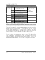
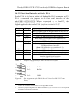
1
phyCORE-167CR/ phyCORE-167CS Hardware Manual Edition November 2002 A product of a PHYTEC Technology Holding company phyCORE-167CR/167CS In this manual are descriptions for copyrighted products that are not explicitly indicated as such. The absence of the trademark () and copyright () symbols does not imply that a product is not protected. Additionally, registered patents and trademarks are similarly not expressly indicated in this manual. The information in this document has been carefully checked and is believed to be entirely reliable. However, PHYTEC Meßtechnik GmbH assumes no responsibility for any inaccuracies. PHYTEC Meßtechnik GmbH neither gives any guarantee nor accepts any liability whatsoever for consequential damages resulting from the use of this manual or its associated product. PHYTEC Meßtechnik GmbH reserves the right to alter the information contained herein without prior notification and accepts no responsibility for any damages which might result. Additionally, PHYTEC Meßtechnik GmbH offers no guarantee nor accepts any liability for damages arising from the improper usage or improper installation of the hardware or software. PHYTEC Meßtechnik GmbH further reserves the right to alter the layout and/or design of the hardware without prior notification and accepts no liability for doing so. Copyright 2002 PHYTEC Meßtechnik GmbH, D-55129 Mainz. Rights including those of translation, reprint, broadcast, photomechanical or similar reproduction and storage or processing in computer systems, in whole or in part are reserved. No reproduction may occur without the express written consent from PHYTEC Meßtechnik GmbH. Address: EUROPE NORTH AMERICA PHYTEC Technologie Holding AG Robert-Koch-Str. 39 D-55129 Mainz GERMANY PHYTEC America LLC 203 Parfitt Way SW, Suite G100 Bainbridge Island, WA 98110 USA Ordering +49 (800) 0749832 Information: [email protected] 1 (800) 278-9913 [email protected] Technical Support: +49 (6131) 9221-31 [email protected] 1 (800) 278-9913 [email protected] Fax: +49 (6131) 9221-33 1 (206) 780-9135 Web Site: http://www.phytec.de http://www.phytec.com 8th Edition: November 2002 PHYTEC Meßtechnik GmbH 2002 L-527e_8 Contents Preface ......................................................................................................1 1 Introduction .........................................................................................3 1.2 Block Diagram..............................................................................6 1.2 View of the phyCORE-167CR/167CS .........................................6 2 Pin Description.....................................................................................7 3 Jumpers ..............................................................................................15 3.1 J1 Use of Pin 30 on the SRAM..................................................19 3.2 J2 Internal or External Program Memory ..................................20 3.3 J3 Flash Addressing...................................................................20 3.4 J4, J5 A/D Reference Voltage ...................................................21 3.5 J6 Oscillator Watchdog / On-Chip Flash...................................22 3.6 J7, J8 Use of the External UART ..............................................22 3.7 J9, J10 Configuration of P3.3, P3.4 for I²C Bus........................23 3.8 J11 RTC Interrupt Output..........................................................24 3.9 J12 Write Protection of EEPROM/FRAM ................................24 3.10 Second Serial Interface Configuration J13, J14 ........................25 3.11 J15 Address of the Serial EEPROM/ FRAM ............................25 3.12 CAN Interfaces J16, J17, J18, J19.............................................26 3.13 J20 Remote Download Source...................................................27 3.14 J21, J22 Serial Interface.............................................................28 3.15 J23, J24 Microcontroller Supply Voltage ..................................29 4 System Configuration........................................................................31 4.1 System Startup Configuration.....................................................31 5 Memory Models .................................................................................35 5.1 Bus Timing .................................................................................39 6 Serial Interfaces .................................................................................41 6.1 RS-232 Interface.........................................................................41 6.2 CAN Interface.............................................................................42 7 The Real-Time Clock RTC-8563 (U10) ...........................................43 8 Serial EEPROM/FRAM (U9)...........................................................44 9 Remote Supervisory Chip (U8) ........................................................45 10 Flash Memory (U1)............................................................................46 11 Battery Buffer and Voltage Supervisor Chip (U13).......................47 12 Technical Specifications....................................................................49 13 Hints for Handling the phyCORE-167CR/167CS ..........................51 PHYTEC Meßtechnik GmbH 2002 L-527e_8 phyCORE-167CR/167CS 14 The phyCORE-167CR/167CS on the phyCORE Development Board HD200 ..................................................................................... 53 14.1 Concept of the phyCORE Development Board HD200............. 53 14.2 Development Board HD200 Connectors and Jumpers............... 55 14.2.1 Connectors..................................................................... 55 14.2.2 Jumpers on the phyCORE Development Board HD200 ................................................................ 57 14.2.3 Unsupported Features and Improper Jumper Settings .. 59 14.3 Functional Components on the phyCORE Development Board HD200 ............................................................................. 60 14.3.1 Power Supply at X1....................................................... 61 14.3.2 Activating the Bootstrap Loader ................................... 63 14.3.3 First Serial Interface at Socket P1A .............................. 65 14.3.4 Second Serial Interface at Socket P1B.......................... 67 14.3.5 First CAN Interface at Plug P2A................................... 72 14.3.6 Second CAN Interface at Plug P2B .............................. 77 14.3.7 Programmable LED D3................................................. 82 14.3.8 Pin Assignment Summary of the phyCORE, the Expansion Bus and the Patch Field ............................... 82 14.3.9 Battery Connector BAT1............................................... 90 14.3.10 Releasing the /NMI Interrupt ........................................ 90 14.3.11 DS2401 Silicon Serial Number ..................................... 90 14.3.12 Pin Header Connector X4 ............................................. 91 15 debugCORE-167CR/167CS ............................................................. 93 15.1 Components of the debugCORE ................................................ 93 15.2 debugADAPTER-167 ................................................................ 95 15.2.1 The Quad-Connector ..................................................... 96 15.3 Physical Dimensions................................................................... 98 Index .................................................................................................... 99 PHYTEC Meßtechnik GmbH 2002 L-527e_8 Contents Index of Figures Figure 1: Block Diagram phyCORE-167CR/167CS....................................6 Figure 2: View of the phyCORE-167CR/167CS .........................................6 Figure 3 Pinout of the phyCORE-connector (Top View, with Cross Section Insert)...............................................................................9 Figure 4: Numbering of the Jumper Pads...................................................15 Figure 5: Location of the Jumpers (Component Side / Soldering Side) ....15 Figure 6: Memory Model Examples ..........................................................38 Figure 7: Physical Dimensions...................................................................49 Figure 8: Modular Development and Expansion Board Concept with the phyCORE-167CR/167CS .............................................54 Figure 9: Location of Connectors on the phyCORE Development Board HD200 .......................................................55 Figure 10: Numbering of Jumper Pads ........................................................57 Figure 11: Location of the Jumpers (View of the Component Side) ...........57 Figure 12: Default Jumper Settings of the phyCORE Development Board HD200 with phyCORE-167CR/167CS ...........................58 Figure 13: Connecting the Supply Voltage at X1 ........................................61 Figure 14: Pin Assignment of the DB-9 Socket P1A as First RS-232 (Front View) ...............................................................................65 Figure 15: Pin Assignment of the DB-9 Socket P1B as Second RS-232 (UART populated, Front View) ....................................69 Figure 16: Pin Assignment of the DB-9 Socket P1B as Emulated RS-232 (Front View) ..................................................................70 Figure 17: Pin Assignment of the DB-9 Plug P2A (CAN Transceiver on phyCORE-167CR/167CS, Front View) ................................72 Figure 18: Pin Assignment of the DB-9 Plug P2A (CAN Transceiver on Development Board)..............................................................73 Figure 19: Pin Assignment of the DB-9 Plug P2A (CAN Transceiver on Development Board with Galvanic Separation) ....................76 PHYTEC Meßtechnik GmbH 2002 L-527e_8 phyCORE-167CR/167CS Figure 20: Pin Assignment of the DB-9 Plug P2B (CAN Transceiver on phyCORE-167CS, only with C167CS) ................................. 77 Figure 21: Pin Assignment of the DB-9 Plug P2B (CAN Transceiver on Development Board, only with C167CS).............................. 78 Figure 22: Pin Assignment of the DB-9 Plug P2B (CAN Transceiver on Development Board with Galvanic Separation, only with C167CS) ............................................................................. 81 Figure 23: Pin Assignment Scheme of the Expansion Bus.......................... 83 Figure 24: Pin Assignment Scheme of the Patch Field................................ 83 Figure 25: Connecting the DS2401 Silicon Serial Number......................... 91 Figure 26: Pin Assignment of the DS2401 Silicon Serial Number.............. 91 Figure 27: Positions of the Additional Components on the debugCORE-167CR/167CS ....................................................... 94 Figure 28: Physical Dimensions debugCORE-167CR/167CS .................... 98 PHYTEC Meßtechnik GmbH 2002 L-527e_8 Contents Index of Tables Table 1: Pinout of the phyCORE-Connector X1 ......................................13 Table 2: Jumper Settings...........................................................................18 Table 3: J1 SRAM Capacity Configuration.............................................19 Table 4: J2 Code Fetch Selection.............................................................20 Table 5: J3 Addressing the Flash .............................................................21 Table 6: J4, J5 A/D Converter Reference Voltage ..................................21 Table 7: J6 Activating the Oscillator Watchdog......................................22 Table 8: J7, J8 Control Signals for Optional External UART .................23 Table 9: J9, J10 I²C Bus Configuration ...................................................23 Table 10: J11 RTC Interrupt Configuration ..............................................24 Table 11: J12 Write Protection of EEPROM/FRAM ................................24 Table 12: J13, J14 Second Serial Interface Configuration ........................25 Table 13: J15 EEPROM/FRAM Address Configuration ..........................25 Table 14: J16, J17, J18, J19 CAN Interface Configuration.......................27 Table 15: J20 Remote Download Source Configuration ...........................27 Table 16: J21, J22 First Serial Interface Configuration.............................28 Table 17: J23, J24 Configuration VCC Pins Microcontroller ...................29 Table 18: Functional Settings on Port P0 for System Startup Configuration..............................................................................32 Table 19: System Startup Configuration Registers.....................................34 Table 20: Memory Device Options for U9 .................................................44 Table 21: Improper Jumper Setting for JP16 on the Development Board ....................................................................59 Table 22: Improper Jumper Setting for JP30/33 on the Development Board ....................................................................59 Table 23: JP9 Configuration of the Main Supply Voltage VCC ...............61 Table 24: JP9 Improper Jumper Settings for the Main Supply Voltage .....62 Table 25: JP28 Configuration of the Boot Button ......................................63 PHYTEC Meßtechnik GmbH 2002 L-527e_8 phyCORE-167CR/167CS Table 26: JP28 Configuration of a Permanent Bootstrap Loader Start ..... 64 Table 27: JP22, JP23, JP10 Configuration of Boot via RS-232 ................ 64 Table 28: Improper Jumper Settings for Boot via RS-232 ......................... 64 Table 29: Jumper Configuration for the First RS-232 Interface ................ 65 Table 30: Improper Jumper Settings for DB-9 Socket P1A as First RS-232 ............................................................................... 66 Table 31: Jumper Configuration of the DB-9 Socket P1B (no second RS-232) .................................................................... 67 Table 32: Improper Jumper Settings for DB-9 Socket P1B (no second RS-232) .................................................................... 68 Table 33: Jumper Configuration of the DB-9 Socket P1B (UART, 2nd RS-232)................................................................... 69 Table 34: Jumper Configuration of the DB-9 Socket P1B (2nd RS-232 via Software Emulation)......................................... 70 Table 35: Improper Jumper Settings for DB-9 Socket P1B (2nd RS-232 via Software Emulation)......................................... 71 Table 36: Jumper Configuration for CAN Plug P2A using the CAN Transceiver on the phyCORE-167CR/167CS ............................ 72 Table 37: Jumper Configuration for CAN Plug P2A using the CAN Transceiver on the Development Board ..................................... 73 Table 38: Improper Jumper Settings for the CAN Plug P2A (CAN Transceiver on the Development Board)......................... 74 Table 39: Jumper Configuration for CAN Plug P2A using the CAN Transceiver on the Development Board with Galvanic Separation ................................................................... 75 Table 40: Improper Jumper Settings for the CAN Plug P2A (CAN Transceiver on Development Board with Galvanic Separation) .................................................................. 76 Table 41: Jumper Configuration for CAN Plug P2B using the CAN Transceiver on the phyCORE-167CS ........................................ 77 Table 42: Jumper Configuration for CAN Plug P2B using the CAN Transceiver on the phyCORE-167CS ........................................ 78 PHYTEC Meßtechnik GmbH 2002 L-527e_8 Contents Table 43: Improper Jumper Settings for the CAN Plug P2B (CAN Transceiver on the Development Board, only with C167CS) ....79 Table 44: Jumper Configuration for CAN Plug P2A using the CAN Transceiver on the Development Board with Galvanic Separation (only with C167CS)..................................................80 Table 45: Improper Jumper Settings for the CAN Plug P2B (CAN Transceiver on Development Board with Galvanic Separation) ..................................................................81 Table 46: JP17 Configuration of the Programmable LED D3...................82 Table 47: Pin Assignment Data/Address Bus for the phyCORE-167CR/167CS / Development Board / Expansion Board.........................................................................84 Table 48: Pin Assignment Port P2, P3, P4 for the phyCORE-167CR/167CS / Development Board / Expansion Board.........................................................................85 Table 49: Pin Assignment Port P5, P6, P7, P8 for the phyCORE-167CR/167CS / Development Board / Expansion Board.........................................................................86 Table 50: Pin Assignment Interface Signals for the phyCORE-167CR/167CS / Development Board / Expansion Board.........................................................................87 Table 51: Pin Assignment Control Signals for the phyCORE-167CR/167CS / Development Board / Expansion Board.........................................................................87 Table 52: Pin Assignment Power Supply for the phyCORE-167CR/167CS / Development Board / Expansion Board.........................................................................88 Table 53: Unused Pins on the phyCORE-167CR/167CS / Development Board / Expansion Board .....................................89 Table 54: JP28 Releasing the /NMI Interrupt ............................................90 Table 55: JP19 Jumper Configuration for Silicon Serial Number Chip .....90 Table 56: Pinout Pin Header Row X3 on the debugCORE-167CR/167CS .......................................................94 Table 57: Connector Layout of the of the Quad-Connector (X6)...............97 PHYTEC Meßtechnik GmbH 2002 L-527e_8 phyCORE-167CR/167CS PHYTEC Meßtechnik GmbH 2002 L-527e_8 Preface Preface This phyCORE-167CR/167CS Hardware Manual describes the board’s design and functions. Precise specifications for Infineon’s C167CR/C167CS microcontroller series controller can be found in the enclosed microcontroller Data Sheet/User's Manual. If software is included please also refer to additional documentation for this software. In this hardware manual and in the attached schematics, low active signals are denoted by a "/" in front of the signal name (i.e.: /RD). A "0" indicates a logic-zero or low-level signal, while a "1" represents a logic-one or high-level signal. Declaration of Electro Magnetic Conformity of the PHYTEC phyCORE-167CR/167CS PHYTEC Single Board Computers (henceforth products) are designed for installation in electrical appliances or as dedicated Evaluation Boards (i.e.: for use as a test and prototype platform for hardware/software development) in laboratory environments. Caution: PHYTEC products lacking protective enclosures are subject to damage by ESD and, hence, may only be unpacked, handled or operated in environments in which sufficient precautionary measures have been taken in respect to ESD-dangers. It is also necessary that only appropriately trained personnel (such as electricians, technicians and engineers) handle and/or operate these products. Moreover, PHYTEC products should not be operated without protection circuitry if connections to the product's pin header rows are longer than 3 m. PHYTEC Meßtechnik GmbH 2002 L-527e_8 1 phyCORE-167CR/167CS PHYTEC products fulfill the norms of the European Union’s Directive for Electro Magnatic Conformity only in accordance to the descriptions and rules of usage indicated in this hardware manual (particularly in respect to the pin header row connectors, power connector and serial interface to a host-PC). Implementation of PHYTEC products into target devices, as well as user modifications and extensions of PHYTEC products, is subject to renewed establishment of conformity to, and certification of, Electro Magnetic Directives. Users should ensure conformance following any modifications to the products as well as implementation of the products into target systems. The phyCORE-167CR/167CS is one of a series of PHYTEC Single Board Computers that can be populated with different controllers and, hence, offers various functions and configurations. PHYTEC supports all common 8- and 16-bit controllers in two ways: (1) as the basis for Rapid Development Kits which serve as a reference and evaluation platform (2) as insert-ready, fully functional micro-, mini- and phyCORE OEM modules, which can be embedded directly into the user’s peripheral hardware, design. PHYTEC's microcontroller modules allow engineers to shorten development horizons, reduce design costs and speed project concepts from design to market. 2 PHYTEC Meßtechnik GmbH 2002 L-527e_8 Introduction 1 Introduction The phyCORE-167CR/167CS belongs to PHYTEC’s phyCORE Single Board Computer module family. The phyCORE SBCs represent the continuous development of PHYTEC Single Board Computer technology. Like its mini-, micro- and nanoMODUL predecessors, the phyCORE boards integrate all core elements of a microcontroller system on a subminiature board and are designed in a manner that ensures their easy expansion and embedding in peripheral hardware developments. As independent research indicates that approximately 70 % of all EMI (Electro Magnetic Interference) problems stem from insufficient supply voltage grounding of electronic components in high frequency environments the phyCORE board design features an increased pin package. The increased pin package allows dedication of approximately 20 % of all pin header connectors on the phyCORE boards to Ground. This improves EMI and EMC characteristics and makes it easier to design complex applications meeting EMI and EMC guidelines using phyCORE boards even in high noise environments. phyCORE boards achieve their small size through modern SMD technology and multi-layer design. In accordance with the complexity of the module, 0402-packaged SMD components and laser-drilled Microvias are used on the boards, providing phyCORE users with access to this cutting edge miniaturization technology for integration into their own design. PHYTEC Meßtechnik GmbH 2002 L-527e_8 3 phyCORE-167CR/167CS The phyCORE-167CR/167CS is a subminiature (60 x 53 mm) insert-ready Single Board Computer populated with Infineon’s C167CR or C167CS microcontroller. Its universal design enables its insertion in a wide range of embedded applications. All controller signals and ports extend from the controller to high-density pitch (0.635 mm) connectors aligning two sides of the board, allowing it to be plugged like a “big chip” into a target application. Precise specifications for the controller populating the board can be found in the applicable controller User’s Manual or Data Sheet. The descriptions in this manual are based on the Infineon C167CR/C167CS. No description of compatible microcontroller derivative functions is included, as such functions are not relevant for the basic functioning of the phyCORE-167CR/167CS. 4 PHYTEC Meßtechnik GmbH 2002 L-527e_8 Introduction The phyCORE-167CR/167CS offers the following features: • subminiature Single Board Computer (60 x 53 mm) achieved through modern SMD technology • populated with the Infineon C167Cx microcontroller (QFP-144 packaging) featuring up to two1 on-chip 2.0B CAN modules • improved interference safety achieved through multi-layer PCB technology and dedicated Ground pins • controller signals and ports extend to two 100-pin high-density (0.635 mm) Molex connectors aligning two sides of the board, enabling it to be plugged like a “big chip” into target application • 16-bit, demultiplexed bus mode • 20 MHz clock frequency (100 ns instruction cycle) • 16 MB address space • 256 kByte to 2 MB external Flash on-board2 • on-board Flash programming, no dedicated Flash programming voltage required through use of 5 V Flash devices • 256 kByte to 1 MB RAM on-board2 • up to 21 CAN interfaces with Philips 82C251 CAN transceiver, or Siliconix’ Si9200EY • I²C Real-Time Clock with internal quartz • 4 to 8 kByte I2C EEPROM1, or 512 Byte to 8 kByte FRAM1 • Voltage Supervisory Chip for Reset logic and power supervision • Remote Supervisory Circuit3 • free Chip Select signals for easy connection of peripheral devices • requires single 5 V / <220 mA supply voltage • RS-232 transceiver for two serial interfaces • optional UART for second asynchronous serial interface • support for modem signals CTS, RTS, DTR, and DSR over the second serial interface (only when populated with external UART) 1 : : 3: 2 Dual on-chip CAN is only available with Infineon‘s C167CS microcontroller. Please contact PHYTEC for more information about additional modul configurations. This feature is under development and not available yet. PHYTEC Meßtechnik GmbH 2002 L-527e_8 5 phyCORE-167CR/167CS 1.1 Block Diagram FLASH UART INFINEON C167CR C167CS P0 P1 RxD0 TxD0 Data Addr 256KB - 2MB Reset RS-232 Transceiver RxD0 / TxD0 RS-232 Transceiver RxD1 / TxD1 CAN Transceiver CAN0H / CAN0L Jumper CAN0 Reset p opt. RxD1 TxD1 CAN1 RAM 256KB-1MB CAN1H / CAN1L CAN Transceiver opt. Digital I / O Ports I2C Bus R e m o t e1 Supervisor EEPROM/ FRAM h y C O R E C o n n e c t o r RTC 1 : This feature is under development and is not available yet. Figure 1: Block Diagram phyCORE-167CR/167CS 1.2 View of the phyCORE-167CR/167CS Figure 2: 6 View of the phyCORE-167CR/167CS PHYTEC Meßtechnik GmbH 2002 L-527e_8 Pin Description 2 Pin Description Please note that all module connections are not to exceed their expressed maximum voltage or current. Maximum signal input values are indicated in the corresponding controller manuals/data sheets. As damage from improper connections varies according to use and application, it is the user’s responsibility to take appropriate safety measures to ensure that the module connections are protected from overloading through connected peripherals. As Figure 3 indicates, all controller signals extend to surface mount technology (SMT) connectors (0.635 mm) lining two sides of the module (referred to as phyCORE-connector). This allows the phyCORE-167CR/167CS to be plugged into any target application like a “big chip”. A new numbering scheme for the pins on the phyCORE-connector has been introduced with the phyCORE specifications. This enables quick and easy identification of desired pins and minimizes errors when matching pins on the phyCORE module with the phyCORE-connector on the appropriate PHYTEC Development Board or in user target circuitry. The numbering scheme for the phyCORE-connector is based on a two dimensional matrix in which column positions are identified by a letter and row position by a number. Pin 1A, for example, is always located in the upper left hand corner of the matrix. The pin numbering values increase moving down on the board. Lettering of the pin connector rows progresses alphabetically from left to right (refer to Figure 3). PHYTEC Meßtechnik GmbH 2002 L-527e_8 7 phyCORE-167CR/167CS The numbered matrix can be aligned with the phyCORE-167CR/167CS (viewed from above; phyCORE-connector pointing down) or with the socket of the corresponding phyCORE Development Board/user target circuitry. The upper left-hand corner of the numbered matrix (pin 1A) is thus covered with the corner of the phyCORE-167CR/167CS marked with a white triangle. The numbering scheme is always in relation to the PCB as viewed from above, even if all connector contacts extend to the bottom of the module. The numbering scheme is thus consistent for both the module’s phyCORE-connector as well as mating connectors on the phyCORE Development Board or target hardware, thereby considerably reducing the risk of pin identification errors. Since the pins are exactly defined according to the numbered matrix previously described, the phyCORE-connector is usually assigned a single designator for its position (X1 for example). In this manner the phyCORE-connector comprises a single, logical unit regardless of the fact that it could consist of more than one physical socketed connector. The location of row 1 on the board is marked by a white triangle on the PCB to allow easy identification. 8 PHYTEC Meßtechnik GmbH 2002 L-527e_8 Pin Description The following figure (Figure 3) illustrates the numbered matrix system. It shows a phyCORE-167CR/167CS with SMT phyCORE-connectors on its underside (defined as dotted lines) mounted on a Development Board. In order to facilitate understanding of the pin assignment scheme, the diagram presents a crossview of the phyCORE module showing these phyCORE-connectors mounted on the underside of the module’s PCB. A B C 1 Figure 3 D 1 Pinout of the phyCORE-connector (Top View, with Cross Section Insert) Many of the controller port pins accessible at the connectors along the edges of the board have been assigned alternate functions that can be activated via software. PHYTEC Meßtechnik GmbH 2002 L-527e_8 9 phyCORE-167CR/167CS Table 1 provides an overview of the pinout of the phyCORE-connector , as well as descriptions of possible alternative functions. Please refer to the Infineon C167Cx User’s Manual/Data Sheet for details on the functions and features of controller signals and port pins. Pin Number Signal Pin Row X1A 1A CLKIN 2A, 7A, 12A, 17A, GND 22A, 27A, 32A, 37A, 42A, 47A 3A P2.9 Description I - Optional external clock generator Ground 0 V I/O /NMI P6.4/ /CS4 ALE WRL A1, A2, A4, A7, A9, A10, A12, A15, A17, A18, A20, A23 D1, D2, D4, D7, D9, D10, D12, D15 /RDY I O O O O CAPCOM1: CC9 Capture Input/Compare Output Fast external Interrupt 1 Input (I) Non-masked interrupt input Chip Select #4 Address latch enable /WRL signal of the microcontroller Address line of the microcontroller I/O Data line of the microcontroller I Microcontroller READY signal input 35A NC - 36A P6.6/ /HLDA I/O 38A, 39A P7.1, P7.3 O 40A, 41A P7.4, P7.6 I/O 43A 44A 45A 46A 48A 49A 50A P3.9 P3.0 P3.1 P3.3 P3.6 P6.0/ /CS0 P6.1/ /CS1 I/O I O O I O O Not connected. These contacts should remain unconnected on the target hardware side. Acknowledge output (master mode)/ input (slave mode) POUT1 PWM Channel 1 POUT3 PWM Channel 3 CAPCOM2:CC28 Capture Input/Compare Output CAPCOM2:CC30 Capture Input/Compare Output SSC Master transmit/Slave receive CAPCOM1 Timer T0 Counter input GPT2 Timer T6 Latch output GPT1 Timer T3 Latch output GPT1 Timer T3 Counter input Chip Select #0 Chip Select #1 4A 5A 6A 8A 9A, 10A, 11A, 13A, 14A, 15A, 16A, 18A, 24A, 25A, 26A, 28A 19A, 20A, 21A, 23A, 29A, 30A, 31A, 33A 34A 10 I/O PHYTEC Meßtechnik GmbH 2002 L-527e_8 Pin Description Pin Number Signal I/O Description Pin Row X1B 1B 2B, 3B P3.15 P2.8, P2.10 O I/O CLKOUT system clock output CAPCOM1: CC8 Capture Input/Compare Output Fast external Interrupt 0 Input (I) CAPCOM1: CC10 Capture Input/Compare Output Fast external Interrupt 2 Input (I) GND - Ground circuitry P6.3/ /CS3 P6.2/ /CS2 /RD A0, A3, A5, A6, A8, A11, A13, A14, A16, A19, A21, A22 D0, D3, D5, D6, D8, D11, D13, D14 P3.12//WRH P6.5//HOLD P6.7//BREQ P7.0, P7.2 O O O O Chip Select #3 Chip Select #2 /RD signal of phyCORE-167CR/167CS Address line of the microcontroller I/O Data line of the microcontroller O I O O 40B, 41B P7.5, P7.7 I/O 42B, 43B, 45B, 46B, 47B, 48B 50B P3.8, P3.13, P3.2, P3.4, P3.5, P3.7 NC I/O Microcontroller /WRH signal Microcontroller /HOLD signal Microcontroller /BREQ signal POUT0 PWM Channel 0 POUT2 PWM Channel 2 CAPCOM2:CC29 Capture Input/Compare Output CAPCOM2:CC31 Capture Input/Compare Output Port 3 of the microcontroller (see corresponding Data Sheet) 4B, 9B, 14B, 19B, 24B, 29B, 34B, 39B, 44B, 49B 5B 6B 7B 8B, 10B, 11B, 12B, 13B, 15B, 16B, 17B, 23B, 25B, 26B, 27B 18B, 20B, 21B, 22B, 28B, 30B, 31B, 32B 33B 35B 36B 37B, 38B PHYTEC Meßtechnik GmbH 2002 - Not connected. These contacts should remain unconnected on the target hardware side. L-527e_8 11 phyCORE-167CR/167CS Pin Number Signal Pin Row X1C 1C, 2C VCC 3C, 7C, 12C, 17C, GND 22C, 27C, 32C, 37C 4C, 5C NC 6C Description - Voltage input +5 = Ground 0 V - Not connected These contacts should remain unconnected on the target hardware side. Battery input for back-up of RTC and buffering of RAM MAX 690/ Power-Fail output Input for startup of FlashTools /RESET input of the phyCORE-167CR/167CS /RESOUT signal of µC Port 2 of the microcontroller (see corresponding Data Sheet) VBAT I 8C 9C 10C 11C 13C, 14C, 15C, 16C, 19C, 20C 18C 21C /PFO BOOT /RESET /RESOUT P2.2, P2.4, P2.5, P2.7, P2.11, P2.12 CAN-H11 RxD1_RS232 O I I O I/O I/O I 23C TxD1_RS232 O 24C 25C 26C 28C 29C 30C 31C 33C 34C 35C, 36C /RTS1_RS232 /CTS1_RS232 /DSR1_RS232 /DTR1_RS232 /RI1_TTL /CD1_TTL SCL IRQ_UART /CS_UART P8.4, P8.6 O I I O I I O O I I/O NC - P5.14 P5.11, P5.9, P5.8, P5.6, P5.3, P5.1, P5.0 VAGND I/O 38C, 39C, 40C 41C, 43C, 44C, 45C, 46C,48C, 49C,50C 42C, 47C 12 I/O - Differential CANH line of second CAN transceiver Input of the second interface series of the phyCORE-167CR/167CS, RS-232 level Output of the second interface series of the phyCORE-167CR/167CS, RS-232 level /RTS signal of the UART U7, RS-232 level /CTS signal of the UART U7, RS-232 level /DSR signal of the UART U7, RS-232 level /DTR signal of the UART U7, RS-232 level /RI signal of the UART U7, TTL level /CD signal of the UART U7, TTL level CLK line I2C bus Interrupt output of the UART U7 Chip Select signal of the UART U7 CAPCOM2:CC20 Capture Input/Compare Output CAPCOM2:CC22 Capture Input/Compare Output Not connected These contacts should remain unconnected on the target hardware side. Port 5 of the microcontroller (see corresponding Data Sheet) Analog Ground of the microcontroller PHYTEC Meßtechnik GmbH 2002 L-527e_8 Pin Description Pin Number Signal Pin Row X1D 1D, 2D VCC 3D, 9D, 14D, 19D, GND 24D, 29D, 34D 4D, 5D VPP I/O Description -- Voltage input +5 V= Ground 0 V - Programming voltage for on-chip Flash. Use only if ST10F168 populates the phyCORE module! These contacts should remain unconnected on the target hardware side when using the C167CR or C167CS. Output of back-up voltage supply for buffering of external components MAX 690 power fail input. If this input is unused, it must be connected to VCC or GND MAX 690 Watchdog input /RESET input of the phyCORE-167CR/167CS Port 2 of the microcontroller (see corresponding Data Sheet) Input of the first serial interface, TTL level Output of the first serial interface, TTL level Differential CANL line of the 2nd CAN transceiver Differential CANL line of the 1st CAN transceiver Differential CANH line of the first CAN transceiver Input of the first serial interface, RS-232 level Output of the first serial interface, RS-232 level CAPCOM1: CC14 Capture Input/Compare Output, Fast ext. Interrupt 6 Input (I) CAPCOM1: CC15 Capture Input/Compare Output Fast external Interrupt 7 Input (I) T7IN Timer T7 Count Input (I) CAPCOM2:CC16 Capture Input/Compare Output CAPCOM2:CC17 Capture Input/Compare Output CAPCOM2:CC18 Capture Input/Compare Output CAPCOM2:CC19 Capture Input/Compare Output Data-line I2C bus Interrupt output of the RTC CAPCOM2:CC21 Capture Input/Compare Output CAPCOM2:CC23 Capture Input/Compare Output CAPCOM1: CC13 Capture Input/Compare Output Fast ext. Interrupt 5 Input (I) Not connected. These contacts should remain unconnected on the target hardware side. Analog Ground Port 5 of the microcontroller (see corresponding Data Sheet) 6D VPD O 7D PFI I 8D 10D 11D, 12D, 13D, 15D 16D 17D 18D 20D 21D 22D 23D 25D 26D WDI /RESET P2.0, P2.1, P2.3, P2.6 P3.11/RxD0 P3.10/TxD0 CAN-L11 CAN-L0 CAN-H0 RxD0_RS232 TxD0_RS232 P2.14, P2.15 I I I/O 27D, 28D, 30D, 31D 32D 33D 35D, 36D P8.0, P8.1, P8.2, P8.3 SDA /IRQ_RTC P8.5, P8.7 O O I/O 37D P2.13 I/O 38D NC - VAGND P5.15, P5.13, P5.12, P5.10, P5.7, P5.5, P5.4, P5.2 VAREF I 39D, 44D, 49D 40D, 41D, 42D, 43D, 45D, 46D, 47D, 48D 50D Table 1: I O I/O I/O I/O I O I/O I/O I Reference voltage input for A/D converter Pinout of the phyCORE-Connector X1 ___________________________________________ 1: Dual on-chip CAN is only available with Infineon C167CS microcontroller. PHYTEC Meßtechnik GmbH 2002 L-527e_8 13 phyCORE-167CR/167CS 14 PHYTEC Meßtechnik GmbH 2002 L-527e_8 Jumpers 3 Jumpers For configuration purposes, the phyCORE-167CR/167CS has 24 solder jumpers, some of which have been installed prior to delivery. Figure 4 illustrates the numbering of the jumper pads, while Figure 5 indicates the location of the jumpers on the board. On the phyCORE-167CR/167CS, only Jumpers J1, J20 and J23 are located on the top side of the circuit board. 1 6 5 e.g.: J20,.. 2 3 4 1 2 3 e.g.: J1, J2, .. 1 2 e.g.: J3, J4, .. Figure 4: Numbering of the Jumper Pads Figure 5: Location of the Jumpers (Component Side / Soldering Side) PHYTEC Meßtechnik GmbH 2002 L-527e_8 15 phyCORE-167CR/167CS The jumpers (J = solder jumper) have the following functions: J1 J2 J3 J4 Default Setting1 (2+3) VCC at pin 30 of the RAM (for RAM < 512 kByte) (2+3) external ROM/ Flash active (closed) Port P4.4 (A20), can be configured as CAN1 receive line2 (closed) VAREF derived from supply voltage VCC J5 (closed) VAGND derived from digital ground GND J6 (open) (open) VAREF from external voltage source via pin X1D50 (open) VAREF from external ground via pins X1C42, X1C47, X1D39, X1D44 and X1D493 (1+2) C167CR: not allowed! (2+3) C167CR: oscillator Watchdog disabled4 (closed) IRQ of the UART is connected to P2.8 of the microcontroller P2.8 of the microcontroller is freely available as standard I/O at pin header row X1B2 (open) /CS2 of the microcon(closed) /CS2 of the microconJ8 troller is freely available at troller is connected to the pin header row X1B6 external UART (open) P3.4 of the microconJ9 (closed) P3.4 of the microcontroller connected to SCL troller is freely available of the I2C bus as standard I/O at pin header row X1B46 (open) P3.3 of the microconJ10 (closed) P3.3 of the microcontroller connected to SDA troller is freely available of the I2C bus as standard I/O at pin header row X1A46 J7 1: 2: 3: 4: 16 (open) C167CR: Oscillator Watchdog enabled4 Alternative Setting (1+2) A18 at pin 30 of the RAM (for RAM > 512 kByte) (1+2) internal ROM/FlashEPROM is active (closed) Address line A20 for external Flash Applies to standard modules without optional features. Dual on-chip CAN is only available with Infineon C167CS microcontroller. These pins are solely connected to GND of the Development Board when using the phyCORE module on a phyCORE Development Board HD200. It is not possible to attach an external GND potential in this configuration. This function is only available with Infineon’s C167CR microcontroller (see corresponding Data Sheet). PHYTEC Meßtechnik GmbH 2002 L-527e_8 Jumpers J11 Default Setting (closed) IRQ of the RTC connected to pin P2.9 of the microcontroller J12 (open) J13 (1+2) J14 (1+2) J15 (2+3) J161 (2+3) J171 (2+3) 1 : 2 : Alternative Setting (open) P2.9 of the controller is freely available as standard I/O at pin header row X1A3 deactivates write (closed) optional write protection protection of the of the EEPROM/FRAM EEPROM/FRAM memory device is memory device activated (see Data Sheet) RS-232 transceiver (TxD) (2+3) RS-232 transceiver of the second serial (TxD) for the second interface connected to serial interface connected P3.0 of the controller to UART (dependens on module configuration) RS-232 transceiver (RxD) (2+3) RS-232 transceiver of the second serial (RxD) for the second interface connected to serial interface connected P3.1 of the controller to UART (dependens on module configuration) address of the serial (1+2) address of the serial memory device at U9 set memory device set to to 0xA8 (hex) (see Data 0xAC (hex) (see Data Sheet of memory device) Sheet of memory device) CAN0 transmit line (1+2) CAN0 transmit line (CANTx) of the CAN (CANTx) of the CAN transceiver at U11 transceiver at U11 connected to P4.6 (A22) connected to P8.1 of the of the microcontroller microcontroller (see (see controller Data controller Data Sheet) 2 Sheet) CAN0 receive line (1+2) CAN0 receive line (CANRx) of the CAN (CANRx) of the CAN transceiver at U11 contransceiver at U11 connected to Port P4.5 (A21) nected to P8.0 of the of the microcontroller microcontroller (see (see controller Data controller Data Sheet)2 Sheet) Note: If the C167CR controller populates the phyCORE module, using the CAN interface reduces the available address space to 1 MB for each /CS signal. Use of port P8 as CAN interface is only possible with Infineon C167CS microcontroller. PHYTEC Meßtechnik GmbH 2002 L-527e_8 17 phyCORE-167CR/167CS J181 J191 J20 Default Setting (2+3) CAN1 transmit line (CANTx) of the CAN transceiver at U12 connected to Port 4.7 (A23) of the controller (see µC Data Sheet) (2+3) CAN1 receive line (CANRx) of the CAN transceiver at U12 connected to Port P4.4 (A20) of the microcontroller (see µC Data Sheet) (open) Remote Download not connected J21 (closed)2 J22 (closed) 2 J23 (closed) J24 (closed) Table 2: 1 : 2 : 18 Alternative Setting (1+2) CAN1 transmit line (CANTx) of the CAN transceiver at U12 connected to P8.3 of the microcontroller (see controller Data Sheet) (1+2) CAN1 receive line (CANRx) of the CAN transceiver at U12 connected to P8.2 of the microcontroller (see controller Data Sheet) (1+2) Remote Download Source at P3.1 (3+5) Remote Download Source CAN1Rx (3+4) Remote Download Source CAN2Rx (2+6) Remote Download Source P3.11 P3.11 used as RXD0 and (open) P3.11 of the controller is conected to RS-232 freely available as transceiver U6 standard I/O at pin header row X1D16 P3.10 used as TXD0 and (open) P3.10 of the controller is conected to RS-232 freely available as transceiver U6 standard I/O at pin header row X1D17 Pin 17 of the controller is (open) Pin 17 of the controller is connected to VCC connected to GND via a bypass capacitor Pin 56 of the controller is (open) Pin 56 of the controller is connected to VCC connected to GND via a bypass capacitor Jumper Settings The second CAN interface is only available with Infineon‘s C167CS (refer to the controller Data Sheet). Note: These jumpers must remain closed on the phyCORE-167CR/167CS. If they are open, no serial communication is possible, hence PHYTEC FlashTools or the BOOT monitor will not function properly. PHYTEC Meßtechnik GmbH 2002 L-527e_8 Jumpers 3.1 J1 Use of Pin 30 on the SRAM Jumper J1 determines the use of pin 30 on the SRAM devices at U2 and U3. On SRAM devices with a capacity of 128 kBytes, pin 30 is defined as an active-high Chip Select signal. To enable access to such SRAM devices, a high-level should be applied to pin 30. On SRAM devices with a capacity of more than 512 kBytes, pin 30 is used as address line A17. In case the SRAM has a 16-bit bus width, this pin must be connected to address line A18 of the microcontroller. On the phyCORE-167CR/167CS, J1 should be used as follows: Jumper J1 must be closed at positions 2+3 if the phyCORE-167CR/167CS is populated with external SRAM devices with a total capacity of 2*128 kByte. This results in a hard-wired connection of VCC to pin 30 of the SRAM. If an SRAM memory configuration of 2*512 kByte is used, pin 30 (A17) on the SRAM must be connected to address line A18 of the microcontroller. This is done by setting Jumper J1 to position 1+2. Please note that a “virtual” 16-bit SRAM memory bus width is achieved by using two parallel 8-bit SRAM devices. Address A0 of the microcontroller enables internal selection of the memory components and is used for generation of the appropriate write signals /WRL and /WRH. The following configurations are possible: SRAM Configuration 2 x 128 kByte SRAM 2 x 512 kByte SRAM J1 2 + 3* 1+2 * = Default setting Table 3: J1 SRAM Capacity Configuration PHYTEC Meßtechnik GmbH 2002 L-527e_8 19 phyCORE-167CR/167CS 3.2 J2 Internal or External Program Memory At the time of delivery, Jumper J2 is closed at 2+3. This default configuration means that the program stored in the external program memory is executed after a hardware reset. In order to allow the execution of a specific controller’s internal program memory, Jumper J2 must be closed at 1+2. The following configurations are possible: Code Fetch Selection Execution from external program memory Execution from internal program memory J2 2 + 3* 1+2 * = Default setting Table 4: J2 Code Fetch Selection 3.3 J3 Flash Addressing Jumper J3 connects the controller’s address line A20 with the address line A19 on the Flash device (U1). If using a Flash memory with a capacity of less than 2 MB, Jumper J3 must remain open in order to avoid conflict with the second CAN interface1. If a 2 MB Flash device populates the phyCORE-167CR/167CS, then Jumper J3 must be closed. In this case, the second CAN interface must be rerouted to and connected at Port P82 in order to avoid conflict with the upper address lines. 1: 2: 20 The second CAN interface is only available on the C167CS controller (refer to the User‘s Manual and Data Sheet). The feature that reroutes CAN signals to port P8 is only available on the C167CS controller. PHYTEC Meßtechnik GmbH 2002 L-527e_8 Jumpers The following configurations are possible: Flash Addressing If Flash memory is < 2 MB, then P4.4 is used as a standard I/O or as CAN1 receive line 1. If Flash memory is > 2 MB, then P4.4 serves as A20 for addressing the Flash (CAN receive line must be connected at Port P8)2. J3 open* closed * = Default setting Table 5: J3 Addressing the Flash 3.4 J4, J5 A/D Reference Voltage The A/D converter on the phyCORE-167CR/167CS requires an upper and lower reference voltage connected at pins 37 and 38 (VAREF, VAGND). The reference voltage source can be selected using Jumpers J4 and J5. A/D Reference Voltage Source Selection External reference voltage source (VAREF at X1D50, VAGND at X1D39, X1D44 and X1D49) VAREF derived from voltage supply VCC VAGND derived from digital ground GND potential J4 J5 open open3 closed* closed* * = Default setting Table 6: 1: 2: 3: J4, J5 A/D Converter Reference Voltage The second CAN interface is only available with Infineon’s C167CS controller (refer to the microcontroller User‘s Manual and Data Sheet for further information). The feature of rerouting CAN signals to port P8 is only available with Infineon’s C167CS controller. These pins are solely connected to GND of the Development Board when using the phyCORE module on a phyCORE Development Board HD200. It is not possible to attach an external GND potential in this configuration. PHYTEC Meßtechnik GmbH 2002 L-527e_8 21 phyCORE-167CR/167CS 3.5 J6 Oscillator Watchdog / On-Chip Flash Depending on the type of microcontroller that populates the phyCORE module, the controller pin 84 has various functions. When using the C167CR, pin 84 controls the oscillator Watchdog. In contrast, when a microcontroller with on-chip Flash populates the module, pin 84 connects the programming voltage. Jumper J6 activates these functions as described in the table below. The following configurations are possible: Function of Pin 84 Activates oscillator Watchdog of the C167CR Disables oscillator Watchdog of the C167CR Connects VPP (12 V) at pin 84 for programming of the on-chip Flash Note: This configuration must not be used in conjunction with an Infineon C167 derivative! J6 open* 2+3 1+2 * = Default setting Table 7: J6 Activating the Oscillator Watchdog 3.6 J7, J8 Use of the External UART An optional UART can populate the phyCORE-167CR/167CS at U7. This configuration allows use of a second serial interface. The controller signal /CS2 activates the external UART. Similar to the C167CR/C167CS’ on-chip UART, serial communication via the external UART can be controlled by an interrupt. In this case, the external interrupt 0 at port P2.8 is used. Jumpers J7 and J8 are used to connect /CS2 and port P2.8 (EX0IN) to the corresponding pins on the external UART. 22 PHYTEC Meßtechnik GmbH 2002 L-527e_8 Jumpers The following configurations are possible: Port P2.8 P2.8 of the microcontroller is freely available as standard I/O at phyCORE-connector pin X1B2 IRQ of the UART connects to the microcontroller at pin P2.8 Chip Select /CS2 /CS2 of the microcontroller is freely available at phyCORE-connector pin X1B6 /CS2 of the microcontroller connects to the external UART J7 open* closed J8 open* closed * = Default setting Table 8: J7, J8 Control Signals for Optional External UART 3.7 J9, J10 Configuration of P3.3, P3.4 for I²C Bus The phyCORE-167CR/167CS is equipped with a Real-Time Clock at U10 and a serial EEPROM/FRAM at U9. Both the Real-Time Clock and the serial EEPROM/FRAM are accessed by means of an I²C interface. With Jumpers J9 and J10, this interface can be connected to port pins P3.3 and P3.4. Use of these pins as standard I/O lines requires opening of the corresponding jumpers. The following configurations are possible: I²C Bus Configuration Port P3.3 used as I/O pin at X1A46 Port P3.3 used as I²C SDA Port P3.4 used as I/O pin at X1B46 Port P3.4 used as I²C SCL J10 open closed* J9 open closed* * = Default setting Table 9: J9, J10 I²C Bus Configuration PHYTEC Meßtechnik GmbH 2002 L-527e_8 23 phyCORE-167CR/167CS 3.8 J11 RTC Interrupt Output Jumper J11 determines whether the interrupt output of the RTC (U10) is connected to port pin P2.9 of the microcontroller. If Jumper J11 remains open, P2.9 can be used as a port pin at X1A3. The following configurations are possible: Port P2.9 Configuration Port P2.9 as I/O pin at X1A3 Port P2.9 as /INT input for RTC J11 open closed* * = Default setting Table 10: J11 RTC Interrupt Configuration 3.9 J12 Write Protection of EEPROM/FRAM Various types of EEPROM/FRAM can populate space U9. Some of these devices provide a write protection function. Closing Jumper J12 connects pin 7 of the serial EEPROM/FRAM with VCC and thus activates write protection. The following configurations are possible: Write Protection EEPROM/FRAM Write protection of EEPROM/FRAM deactivated Write protection of EEPROM/FRAM activated J12 open* closed * = Default setting Table 11: 24 J12 Write Protection of EEPROM/FRAM PHYTEC Meßtechnik GmbH 2002 L-527e_8 Jumpers 3.10 Second Serial Interface Configuration J13, J14 Jumpers J13 and J14 enable selection of the signal source of the second serial interface. As an alternate to the software-emulated interface at port pins P3.0 and P3.1 of the controller, an optional external UART can be installed on the phyCORE-167CR/167CS at U7. With the implementation of the external UART, the port pins can be used as standard I/O pins at X1A44 (P3.0) and X1A45 (P3.1). The following configurations are possible: RS-232 Interface Configuration P3.0 and P3.1 connect to RS-232 transceiver for software-emulated second serial interface UART U7 connect to RS-232 transceiver providing a real second interface J13 1 + 2* J14 1 + 2* 2+3 2+3 * = Default setting Table 12: 3.11 J13, J14 Second Serial Interface Configuration J15 Address of the Serial EEPROM/ FRAM Jumper J15 configures the serial EEPROM/FRAM address. The default configuration (J15 = 2+3) sets the address to 0xA8. The following configurations are possible: EEPROM/FRAM Address 0xA8 0xAC J15 2 + 3* 1+2 * = Default setting Table 13: J15 EEPROM/FRAM Address Configuration PHYTEC Meßtechnik GmbH 2002 L-527e_8 25 phyCORE-167CR/167CS 3.12 CAN Interfaces J16, J17, J18, J19 The first CAN interface of the phyCORE-167CR/167CS is available at the port pins P4.5 (CAN1Rx) and P4.6 (CAN1Tx, as well as CAN2Tx1). The second CAN2 interface is located at port pins P4.4 (CAN2Rx) and P4.7 (CAN2Tx, as well as CAN1Rx or CAN2Rx1). These signals extend to the two CAN transceivers at U11 and U12 (PCA82C251, alternately Si9200EY). The CAN transceivers generate the corresponding CANH0, CANL0, CANH1, and CANL1 signals. These signals can be directly connected to a CAN dual-wire bus. Generation of the CAN signals requires closing the solder Jumpers J16, J17, J18, and J19. Direct access to the CAN1Rx, CAN1Tx, CAN2Rx and CAN2Tx signals is also available at the module’s X1 pin header row if soldering jumpers J16, J17, J18 and J19 are open. This enables use of an external CAN transceiver. In order to utilize the full 16 MB linear address space of the microcontroller, the CAN interface signals can be optionally routed to port 83. In this case Jumpers J16 - J19 must be set at positions 1+2. Please refer to the Infineon C167 User’s Manual/Data Sheet for details on the functions and features of controller signals and port pins. Note: If the C167CR controller populates the phyCORE module, using the CAN interface reduces the available address space to 1 MB for each /CS signal. 1: 2: 3: 26 The C167CS allows for optional use of various CAN signals on this port. Configuration is made using the SFR (special function register) PCIR. When using the on-board CAN transceivers we recommend to use the signals as indicated in the table below. The second CAN interface is only available with Infineon’s C167CS controller. The feature of rerouting CAN signals to port P8 is only available with Infineon’s C167CS controller. Caution: Ensure correct configuration of the bit field IPC (in controller register PCIR) to allow proper use of the CAN interface (refer to the microcontroller User‘s Manual and Data Sheet for further information). PHYTEC Meßtechnik GmbH 2002 L-527e_8 Jumpers The following CAN interface configurations are possible: Interface CAN1 P4.5 (CAN1Rx) P4.6 (CAN1Tx) P8.0 (CAN1Rx) P8.1 (CAN1Tx)1 J16 2 + 3* J17 2 + 3* 1+2 1+2 Interface CAN22 P4.4 (CAN2Rx) P4.7 (CAN2Tx) P8.2 (CAN2Rx) P8.3 (CAN2Tx) 1 J18 J19 2 + 3* 2 + 3* 1+2 1+2 * = Default setting Table 14: 3.13 J16, J17, J18, J19 CAN Interface Configuration J20 Remote Download Source Space U8 on the module is intended to be populated by a Remote Supervisory Chip3. This IC can initiate a boot sequence via various serial interfaces (refer to section 6). Jumper J20 is reserved for future use and remains open as default. The following configurations are possible: Download Source not available Port P3.11 / RxD0 Port P3.1 / RxD1 Port CAN1Rx Port CAN2Rx J20 open* 2+6 1+2 3+5 3+4 * = Default setting Table 15: 1: 2: 3: J20 Remote Download Source Configuration Rerouting CAN signals to port P8 is only available with Infineon’s C167CS controller. Caution: Ensure correct configuration of the bit field IPC (in controller register PCIR) to allow proper use of the CAN interface (refer to the microcontroller User‘s Manual and Data Sheet for further information). The second CAN interface is only available with Infineon’s C167CS controller. This feature is under development and not available at this time. PHYTEC Meßtechnik GmbH 2002 L-527e_8 27 phyCORE-167CR/167CS 3.14 J21, J22 Serial Interface Jumper J21 and J22 connect the signals of the first asynchronous serial interface to the on-board RS-232 transceiver (U6). The interface signals are then available with RS-232 level at the phyCORE-connector pins X1D22 (RxD0) and X1D23 (TxD0). If the jumpers are opened, the applicable controller pins P3.10 and P3.11 can be used with their alternative functions or the serial interface signals are available with their TTL level at phyCORE-connector pins X1D17 and X1D16. Note: These jumpers must remain closed on the phyCORE-167CR/167CS. If they are open, no serial communication is possible, hence PHYTEC FlashTools or the BOOT monitor will not function properly. If the jumpers are closed we recommend not to use the interface signals with their TTL level as this will cause damage to the on-board components. Signal Quality TxD0 and RxD0 carry RS-232 level P3.10 and P3.11 available as I/O pin or TxD0 and RxD0 interface signals with TTL level J21 closed* open J22 closed* open * = Default setting Table 16: 28 J21, J22 First Serial Interface Configuration PHYTEC Meßtechnik GmbH 2002 L-527e_8 Jumpers 3.15 J23, J24 Microcontroller Supply Voltage Jumper J23 and J24 connect certain controller pins to their required supply potential. Note: Jumper J23 and J24 must be closed in conjunction with the Infineon C167CR or C167CS Microcontroller. VCC Pin Connection VCC connected to controller pins C16 and C17 function as bypass capacitors *1 2 J23 1 closed* J24 1 closed* open2 open2 Default setting phyCORE-167CR/167CS Must not be used on phyCORE-167CR/167CS! Table 17: J23, J24 Configuration VCC Pins Microcontroller PHYTEC Meßtechnik GmbH 2002 L-527e_8 29 phyCORE-167CR/167CS 30 PHYTEC Meßtechnik GmbH 2002 L-527e_8 System Configuration 4 System Configuration Following a hardware or software reset, the microcontroller starts program execution from address 00:0000H. At this address a jump instruction to an application-specific initialization routine is located. This routine configures certain features of the microcontroller. Initialization is carried out in a privileged mode and completed by an EINIT instruction. After that, access to specific registers and execution of certain instructions are limited. Although most features of the C167CR/C167CS microcontroller are configured and/or programmed during the initialization routine, other features, which influence program execution, must be configured prior to initialization. 4.1 System Startup Configuration The system startup configuration sets the features of the microcontroller that have a direct influence on program execution and, hence, the correct execution of the initialization routine as well. Of particular importance to the system startup configuration are the characteristics of the external bus interface which supports the module’s memory (for example data width, multiplexed- or demultiplexed mode). During the system startup configuration, certain pins comprising port P0 are latched by the controller during the reset procedure. The signal level on the corresponding input pins configures the resulting characteristics of the controller. The system startup configuration can be set by connecting desired pins at port 0 with a pull-down resistor (resulting in logical 0), or by leaving the connections open (resulting in logical 1). A 4.7 kΩ pull-down resistor is recommended, although the resistor value is also dependent upon the external circuitry that is connected to the data bus of the module. PHYTEC Meßtechnik GmbH 2002 L-527e_8 31 phyCORE-167CR/167CS The individual pins of port P0 have the following functions: Function of port P0 during system reset (high byte) Bit H7 H6 H5 CLKCFG R31, R29, 1 1 H4 H3 SALSEL R27 R26 0(11) 0 R28 1 H2 H1 Bit H0 CSSEL R25 R24 0 0 WRC R23 0 Function of port P0 during system reset (low byte) Bit L7 L6 L5 L4 L3 L2 L1 Bit L0 BUSTYP SMOD ADP EMU R22 R21 1 0 Pin 21B 0 Pin 20B Pin 20A Pin 19A Pin 18B Table 18: Functional Settings on Port P0 for System Startup Configuration In order to ensure proper functioning of the microcontroller, reserved pins must remain at high-level (logical 1). Configuration on these pins must not be changed. 1: 32 On modules with a memory configuration featuring 2 MB Flash memory (PCM-009-x3x ) the register SALSEL must be configured with the values 1 (H4) 0 (H3). PHYTEC Meßtechnik GmbH 2002 L-527e_8 System Configuration The following table provides detailed comments to these system startup functions: Name Value Function CLKCFG 1 1 1* CPU clock = ext. clock * 4 1 1 0 CPU clock = ext. clock * 3 1 0 1 CPU clock = ext. clock * 2 1 0 0 CPU clock = ext. clock * 5 0 1 1 CPU clock = ext. clock * 1 0 1 01 CPU clock = ext. clock * 1.5 0 0 11 CPU clock = ext. clock * 0.5 0 0 01 CPU clock = ext. clock * 2.5 SALSEL 1 1 address lines A16..A17, I/O pins P4.2..P4.7 23 1 0 address lines A16..A23, no I/O pins 0 1 no address lines, I/O pins P4.0..P4.7 2 0 0 address lines, A16..A19, I/O pins P4.4..P4.7 CSSEL 1 1 Chip Selects /CS0../CS4, no I/O pins 1 0 no Chip Selects, I/O pins P6.0..P6.4 0 1 Chip Selects /CS0../CS1, I/O pins P6.2..P6.4 0 0 Chip Selects /CS0../CS2, I/O pins P6.3..P6.4 WRC 1 /WR and /BHE 0* /WRL and /WRH 1: 2: 3: Comment defines CPU clock defines function of port pins P4.0..P4.7 defines function of port pins P6.0..P6.4 defines function of pins /WR and P3.12 These configurations are only possible with an Infineon C167CS. On modules with a memory configuration featuring 2 MB Flash memory (PCM-009-x3x ) the register SALSEL must be configured with the values 1 (H4) 0 (H3). Note: If the C167CR controller populates the phyCORE module, using the CAN interface reduces the available address space to 1 MB for each /CS signal. PHYTEC Meßtechnik GmbH 2002 L-527e_8 33 phyCORE-167CR/167CS Name Value Function BUSTYP 1 1 16-bit multiplexed bus BSL ADP EMU Table 19: 10 16-bit demultiplexed bus 01 00 1 0 1 0 1 0 8-bit multiplexed bus 8-bit demultiplexed bus Bootstrap loader inactive Bootstrap loader active adapter mode inactive adapter mode active emulation mode inactive emulation mode active Comment defines bus interface for /CS0 (BUSCON0) System Startup Configuration Registers Default system startup configuration of the phyCORE-167CR/167CS The initial setting of the system startup configuration can be modified during the initialization routine. Certain functions can not be configured during startup, such as selection of the number of wait states for individual memory devices and Chip Select signals, as well as the location of these devices within the controller’s address space. Several software development tools utilize a special file which allows easy definition of system settings. This configuration file can be easily included in the translation and link procedures (such as the start167.a66 used within the Keil software development tool chain). 34 PHYTEC Meßtechnik GmbH 2002 L-527e_8 Memory Models 5 Memory Models The C167CR/C167CS controller provides up to five Chip Select signals at port P6 for easy selection of external peripherals or memory banks. Depending on the number of memory devices installed on the phyCORE-167CR/167CS, as well as the availability of the optional UART, up to three Chip Select signals are used internally. /CS0 (P6.0) selects the Flash memory installed on U1 with a total memory of either 256 kByte, 512 kByte, 1 MB or 2 MB. The external data memory consists of the one RAM bank at U2/U3. These spaces can house memory devices of 128 kByte or 512 kByte in an SO28-32 package. /CS1 (P6.1) selects the RAM bank on U2/U3. /CS2 (P6.2) selects the optional UART at U7. The Chip Select signals must be enabled during reset (refer to section 4). The assignment of the Chip Select signals to specific address areas is done with the corresponding ADDRESELx and BUSCONx register. Note that ADDRESELx must be configured prior activating of the Chip Select signal with register BUSCONx. Ensure that the memory areas do not overlap in order to avoid conflicts when accessing the desired code or data memory. Program code must remain accessible via /CS0. Prior to definition of the ADDRESELx and the BUSCONx register, only /CS0 (P6.0 connected to Flash bank 0) is active in the entire address space and remains active for all areas not assigned to another Chip Select signal. By configuring the memory cycle wait state (Tc = 50 ns) and the read/write delay it is possible to use memory devices with access times up to 100 ns at a bus cycle time of 150 ns. To run the controller without wait state, memory devices with 55 ns access time must be installed. In this case, the bus cycle time is 100 ns. The read/write delay should be always active (refer to the C167CR/C167CS User’s Manual for more information). PHYTEC Meßtechnik GmbH 2002 L-527e_8 35 phyCORE-167CR/167CS The following paragraph contains important information on timing characteristics. All information refers to a C167CR/C167CS controller with a 16-bit bus, demultiplexed, at 20 MHz CPU clock time (Fosz). Tc = 50 ns * wait state control (MCTC in BUSCON) Tf = 50 ns * tristate control (MTTC in BUSCON). addresses stable until data valid: /RD low until data valid: /RD low until data valid (rd/wr delay): /RD high until databus high-Z: /RD high until data high-Z (rd/wr delay): /CSx until data valid: /RD and /WR low: /RD and /WR low (rd/wr delay): data valid until /WR high: /WR high until data invalid: max. 70 ns + Tc max. 55 ns + Tc max. 30 ns + Tc max. 15 ns + Tf max. 35 ns + Tf max. 55 ns + Tc min. 65 ns + Tc min. 40 ns + Tc min. 25 ns + Tc min. 15 ns + Tf SR 1 SR1 SR1 SR1 SR1 SR1 CC2 CC2 CC2 CC2 The following examples contain two configurations of the controller’s memory areas given the standard memory devices populating the phyCORE-167CR/167CS. These examples match the needs of most standard applications. 1: 2: 36 SR = System Time (external circuitry must meet this timing criteria) CC = Controller Characteristic (the controller ensures this time for external peripheral circuitry) PHYTEC Meßtechnik GmbH 2002 L-527e_8 Memory Models Example a) ADDRESEL1: 0406h = address range 04:0000h - 07:FFFFh (256 kByte RAM bank on U2/U3) ADDRESEL2: 0800h = address range 08:0000h - 08:0FFFh (4 kByte address space for ext. UART) ADDRESEL31: 0816h = address range 08:1000h – 0C:FFFFh (256 kByte free I/O area) ADDRESEL41: 0C16h = address range 0C:1000h - 10:0FFFh (256 kByte free I/O area) BUSCON0: 04AFh: bus active for /CS0 (Flash bank U1) BUSCON1: 04AFh: bus active for /CS1 (RAM bank U2/3) BUSCON2: 042Fh: bus active for /CS2 (ext. UART) BUSCON31: 068Fh: bus active for /CS3 (free I/O) 1 BUSCON4 : 068Ch: bus active for /CS4 (free I/O) BUSCON0-2: for all 55 ns memory devices (0 wait states, read/write delay, no tristate, short ALE, 16-bit demultiplexed) BUSCON3,4: for free I/O area (3 wait states, read/write delay, tristate wait 300 ns, long ALE, 16-bit demultiplexed) Example b) ADDRESEL1: 0006h = address range 00:0000h - 03:FFFFh (256 kByte RAM bank on U2/3) ADDRESEL2: 0806h = address range 08:0000h - 08:0FFFh (4 kByte address space for external UART) ADDRESEL31: 0816h = address range 08:1000h – 0C:0FFFh (256 kByte free I/O) ADDRESEL41: 0C16h = address range 0C:1000h - 10:0FFFh (256 kByte free I/O) BUSCON0: 04AFh: bus active for /CS0 (Flash bank U1) BUSCON1: 04AFh: bus active for /CS1 (RAM bank U2/3) BUSCON2: 042Fh: bus active for /CS2 (external UART) 068Ch: bus active for /CS3 (free I/O) BUSCON31: 1 BUSCON4 : 068Ch: bus active for /CS4 (free I/O) BUSCON0-2: for all 55 ns memory devices active (0 wait states, read/write delay, no tristate, short ALE, 16-bit demultiplexed) BUSCON3,4: for free I/O area (3 wait states, read/write delay, tristate, long ALE, 16-bit demultiplexed) 1: /CS3 and /CS4 are not active in the standard configuration of the phyCORE-167CR/167CS. In order to use these signals, resistors R24 and R25 must be removed (refer to section 4.1). PHYTEC Meßtechnik GmbH 2002 L-527e_8 37 phyCORE-167CR/167CS Example a) FF:FFFFh 10:1000h 10:0FFFh 0C:1000h OC:0FFFh 08:1000h P6.0 (/CS0) memory image of Flash Bank 1 Example b) FF:FFFFh 10:1000h 10:0FFFh 256 kByte I/O P6.4 (/CS4) 256 kByte I/O P6.3 (/CS3) 0C:1000h OC:0FFFh 08:1000h 08:0FFFh 08:0FFFh 4 kByte 07:FFFFh P6.2 (/CS2) 256 kByte 08:0000h 07:FFFFh 03:FFFFh P6.1 (/CS1) 256 kByte 04:0000h 03:FFFFh Figure 6: 38 P6.0 (/CS0) 256 kByte I/O P6.3 (/CS3) 4 kByte P6.2 (/CS2) 256 kByte P6.0 (/CS0) 256 kByte RAM Bank U2/U3 FLASH Bank U1 00:0000h P6.4 (/CS4) FLASH Bank U1 RAM Bank U2/U3 04:0000h 256 kByte I/O external UART external UART 08:0000h P6.0 (/CS0) memory image of Flash Bank 1 00:0000h P6.1 (/CS1) Memory Model Examples PHYTEC Meßtechnik GmbH 2002 L-527e_8 Memory Models 5.1 Bus Timing To enable connection of external memory components, the BUSCON register should be configured as follows: BUSCONx: 04AEh: • 1 wait state • read/write delay • no tristate • short ALE • 16-bit demultiplexed • address /CSx active This configuration is valid for all memory devices on the phyCORE-167CR/167CS with up to 70 ns access time. It activates a wait state and the read/write delay. The configuration of one wait state (1 wait state: Tc = 50 ns) and a read/write delay supports memory devices with up to 70 ns access time with a bus cycle of 150 ns. PHYTEC Meßtechnik GmbH 2002 L-527e_8 39 phyCORE-167CR/167CS 40 PHYTEC Meßtechnik GmbH 2002 L-527e_8 Serial Interfaces 6 Serial Interfaces 6.1 RS-232 Interface One RS-232 transceiver is located on the phyCORE-167CR/167CS at U6. This device converts the signal levels for the P3.11/RxD0 and P3.10/TxD0 lines, as well as those of the second serial interface, P3.1/RxD1 and P3.0/TxD1 from TTL level to RS-232 level. Use of the optional UART on U7 requires changing the jumper settings for J13 and J14 to 2+3 (refer to section 3.10) in order to route the RxD and TxD signals to the transceiver. As an alternative, a second RS-232 interface can be established by software emulation on port P3.0 and P3.1 with J13 and J14 closed at position 2+3. The RS-232 interface enables connection of the module to a COM port on a host-PC. In this instance the RxD0 line of the transceiver is connected to the TxD line of the COM port; while the TxD0 line is connected to the RxD line of the COM port. The Ground potential of the phyCORE-167CR/167CS circuitry needs to be connected to the applicable Ground pin on the COM port as well. The microcontroller’s on-chip UART does not support handshake signal communication. However, depending on user needs, handshake communication can be software emulated using port pins on the microcontroller. Use of an RS-232 signal level in support of handshake communication requires use of an external RS-232 transceiver not located on the module. If the module is populated with a UART device at U7, a supplemental RS-232 transceiver can be mounted at position U5. This latter device enables RS-232 signal conversion of the handshake signals supported by the external UART. Note: Jumpers J21 and J22 must remain closed on the phyCORE-167CR/167CS. If they are open, no serial communication is possible, hence PHYTEC FlashTools or the BOOT monitor will not function properly. PHYTEC Meßtechnik GmbH 2002 L-527e_8 41 phyCORE-167CR/167CS 6.2 CAN Interface The phyCORE-167CR/167CS is designed to house two CAN transceivers at U11 and U12 (either PCA82C251 or Si9200EY). The CAN bus transceiver devices support signal conversion of the CAN transmit (CANTx) and receive (CANRx)lines. The CAN transceiver supports up to 110 nodes on a single CAN bus. Data transmission occurs with differential signals between CANH and CANL. A Ground connection between nodes on a CAN bus is not required, yet is recommended to better protect the network from electromagnetic interference (EMI). In order to ensure proper message transmission via the CAN bus, a 120 Ohm termination resistor must be connected to each end of the CAN bus. For larger CAN bus systems, an external opto-coupler should be implemented to galvanically separate the CAN transceiver and the phyCORE-167CR/167CS. This requires the CANTx and CANRx lines to be separated from the on-board CAN transceivers by opening Jumpers J16, J17, J18, and J19. For connection of the CANTx and CANRx lines to an external transceiver we recommend using a Hewlett Packard HCPL06xx or a Toshiba TLP113 HCPL06xx fast opto-coupler. Parameters for configuring a proper CAN bus system can be found in the DS102 norms from the CiA1 (CAN in Automation) User and Manufacturer’s Interest Group. Note: If the C167CR controller populates the phyCORE module, using the CAN interface reduces the available address space to 1 MB for each /CS signal. ___________________________ CiA: CAN in Automation. Founded in March 1992, CiA provides technical, product and marketing information with the aim of fostering Controller Area Network’s image and providing a path for future developments of the CAN protocol. 1: 42 PHYTEC Meßtechnik GmbH 2002 L-527e_8 Real-Time Clock RTC-8563 7 The Real-Time Clock RTC-8563 (U10) For real-time or time-driven applications, the phyCORE-167CR/167CS is equipped with an RTC-8563 Real-Time Clock at U10. This RTC device provides the following features: • Serial input/output bus (I2C) • Power consumption Bus active: max. 50 mA Bus inactive, CLKOUT = 32 kHz : max. 1.7 µA Bus inactive, CLKOUT = 0 kHz : max. 0.75 µA • Clock function with four year calendar • Century bit for year 2000-compliance • Universal timer with alarm and overflow indication • 24-hour format • Automatic word address incrementing • Programmable alarm, timer and interrupt functions If the phyCORE-167CR/167CS is equipped with a battery, the Real-Time Clock runs independently of the board’s power supply. Programming the Real-Time Clock is done via the I2C bus (address 0 x A2 = 1010001), which is connected to port P3.4 (SCL) and port P3.3 (SDA). The Real-Time Clock also provides an interrupt output that extends to port P2.9 via Jumper J11. An interrupt occurs in case of a clock alarm, timer alarm, timer overflow and event counter alarm. An interrupt must be cleared by software. With the interrupt function, the Real-Time Clock can be utilized in various applications. For more information on the features of the RTC-8563, refer to the corresponding Data Sheet. Note: After connection of the supply voltage, or after a reset, the Real-Time Clock generates no interrupt. The RTC must first be initialized (see RTC Data Sheet for more information) PHYTEC Meßtechnik GmbH 2002 L-527e_8 43 phyCORE-167CR/167CS 8 Serial EEPROM/FRAM (U9) The phyCORE-167CR/167CS is populated with a non-volatile memory with a serial interface (I2C interface) to store configuration data. According to the memory configuration of the module, an EEPROM (4 to 32 kByte) or FRAM can be mounted at U9. A description of the I2C memory protocol of the specific memory component at U9 can be found in the respective Data Sheet. Table 20 gives an overview of the memory components that can be used at U9 at the time of printing of this manual. Device Type EEPROM FRAM Table 20: Size 4 kByte 8 kByte 32 kByte 512 Byte 8 kByte Component 24WC32 24WC64 24WC256 FM24C04 FM24C64 Manufacturer Catalyst, Microchip Catalyst, Microchip Microchip Ramtron Ramtron Memory Device Options for U9 Various available EEPROM/FRAM types provide a write protection function1. Jumper J12 is used to activate this function. If this jumper is closed, then pin 7 of the serial EEPROM/FRAM is connected to VCC. Refer to section 3.9 for details on jumper settings for J12. Jumper J15 configures the address of the serial EEPROM/FRAM. The default configuration (J15 = 2+3) sets the address to 0xA8. Refer to section 3.11 for details on jumper settings for J15. ______________________ 1: 44 Refer to the corresponding EEPROM/FRAM Data Sheet for more information on the write protection function. PHYTEC Meßtechnik GmbH 2002 L-527e_8 Remote Supervisory Chip 9 Remote Supervisory Chip (U8) Space U8 is intended to be populated by a Remote Supervisory Chip1. This IC can initiate a boot sequence via a serial interface, such as RS-232 or CAN. The RSC can start the PHYTEC FlashTools without requiring a manual release of the boot sequence on the phyCORE module applied via a BOOT jumper or button. This enables a remote controlled software update of the on-board Flash device. This function can be controlled by various interfaces. Solder Jumper J20 configures the remote download source. The Remote Supervisory Chip is under development and not available at this time. Accordingly, Jumper J20 remains open in the default configuration. Refer to section 3.13 for details on jumper settings for J20. This feature will be available on future phyCORE modules. _______________________ 1: This feature is under development and not available at this time. PHYTEC Meßtechnik GmbH 2002 L-527e_8 45 phyCORE-167CR/167CS 10 Flash Memory (U1) Use of Flash as non-volatile memory on the phyCORE-167CR/167CS provides an easily reprogrammable means of code storage. The following Flash devices can populate the phyCORE-167CR/167CS: • • • • 29F200 with 1* 16 kByte, 2* 8 kByte, 1* 32 kByte, 3* 64 kByte 29F400 with 1* 16 kByte, 2* 8 kByte, 1* 32 kByte, 7* 64 kByte 29F800 with 1* 16 kByte, 2* 8 kByte, 1* 32 kByte, 15* 64 kByte 29F160 with 1* 16 kByte, 2* 8 kByte, 1* 32 kByte, 31* 64 kByte These Flash devices are programmable with 5 V. No dedicated programming voltage is required. Use of a Flash device as the only code memory results in no or only a limited usability of the Flash memory as non-volatile memory for data. This is due to the internal structure of the Flash device as, during the Flash-internal programming process, the reading of data from Flash is not possible. Hence, for Flash programming, program execution must be transferred out of Flash (such as into von Neumann RAM). This usually equals the interruption of a "normal" program execution cycle. As of the printing of this manual, Flash devices generally have a life expectancy of at least 100.000 erase/program cycles. 46 PHYTEC Meßtechnik GmbH 2002 L-527e_8 Battery Buffer and Voltage Supervisor Chip 11 Battery Buffer and Voltage Supervisor Chip (U13) The battery that buffers the memory is not essential to the functioning of the phyCORE-167CR/167CS. However, this battery buffer embodies an economical and practical means of storing non-volatile data. It is necessary to preserve data from the Real-Time Clock in case of a power failure. The VBAT input at pin X1C6 of the board is provided for connecting the external battery. The negative polarity pin on the battery must be connected to GND on the phyCORE-167CR/167CS. As of the printing of this manual, a lithium battery is recommended as it offers relatively high capacity at low discharge. In the event of a power failure at VCC, the RAM memory and the RTC will be buffered by a connected battery via VBAT. The RTC and the SRAM devices are generally supplied via VPD in order to preserve data by means of the battery back-up in the absence of a power supply via VCC. The back-up battery is designed to buffer only SRAM devices as installed in the standard configuration of the module. The standard SRAM device has a power consumption of 1 µA in Power Down mode. When installing a different SRAM device, ensure that the current draw in Power Down mode does not exceed 1 µA. Faster SRAMs have an increased power consumption that can cause fast battery discharge. Power consumption depends on the installed components and memory size (see section 12, "Technical Specifications“). Note: Be advised that despite the battery buffer, changes in the data content within the RAM can occur. The battery buffer does not completely remove the danger of data destruction. PHYTEC Meßtechnik GmbH 2002 L-527e_8 47 phyCORE-167CR/167CS The Voltage Supervisor Chip populating U13 controls switching between VCC supply and the back-up battery. Furthermore, the Voltage Supervisor Chip is used to generate a definite release of a reset signal if the supply voltage VCC drops below 4.65 V. This ensures the proper start-up of the microcontroller. The basic characteristics of this IC are described in the appropriate Data Sheet, which is available on the Spectrum CD. All pins of the Voltage Supervisor Chip are routed to the phyCORE-connector. The VPD voltage is available on the OUT pin of the Voltage Supervisor Chip. In normal operation mode, this pin is supplied by VCC (via a diode). Additionally, VBAT is routed via the voltage divider R9/R10 to pin PFI. If VBAT = 3.3 V, a voltage of 1.65 V is available at PFI. If the voltage at PFI drops below 1.25 V, the signal /PFO is released. The signals WDI and /PFO are available at the phyCORE-connector pins X1D7 and X1C8. 48 PHYTEC Meßtechnik GmbH 2002 L-527e_8 Technical Specifications 12 Technical Specifications The physical dimensions of the phyCORE-167CR/167CS are represented in Figure 7. The module’s profile is ca. 6 mm thick, with a maximum component height of 2.0 mm on the backside of the PCB and approximately 2.5 mm on the front side. The board itself is approximately 1.5 mm thick. 60.2 ± a 55.39 ± a 53.92 ± a 47.6 ± b 50.58 ± b 6.32 ± a 49.33 ± a 52.84 ± a 49.33 ± b 2.34 ± a 8.90 ± a 8.90 ± a 4.82 ± a ∅ 2.7 ± b Tolerance in [mm] Figure 7: a 0.20 b 0.05 Physical Dimensions PHYTEC Meßtechnik GmbH 2002 L-527e_8 49 phyCORE-167CR/167CS Additional specifications: • • Dimensions: Weight: • • Storage temperature: Operating temperature: • • • Humidity: Operating voltage: Power consumption: maximum 220 mA typical 110 mA maximum 100 µA typical 2 µA (RAM) typ. 1 µA Real-Time Clock 60 mm x 53 mm approximately 25 g with all optional components mounted on the circuit board -40°C to +90°C standard: 0°C to +70°C extended: -40°C to +85°C 95 % r.F. not condensed 5 V ±5 %, VBAT 3 V ±20 % Conditions: VCC = 5 V, VBAT = 0 V, 256 kByte RAM, 5 MHz quartz, 20°C VCC = 0 V, VBAT = 3 V, 20°C These specifications describe the standard configuration of the phyCORE-167CR/167CS as of the printing of this manual. Please note that the module storage temperature is only 0°C to +70°C if a battery buffer is used for the RAM devices. 50 PHYTEC Meßtechnik GmbH 2002 L-527e_8 Hints for Handling the Module 13 Hints for Handling the phyCORE-167CR/167CS All C167 compatible controllers (C167CR, C167CS, etc.) can populate the phyCORE-167CR/167CS module at U4. Please note that, if using a C167Cx derivative with an active CAN interface via port 4, only 20 external address lines (A0…A19) and 1 MB of address space is available on the module. These constraints can be avoided by relocating the CAN interface to port 81 (see controller User’s Manual and Data Sheet for details). In order to activate the address lines A18…A23 (for more than 256 kByte Flash) the configuration resistors at data lines D12 and D11 of the module must be pulled to GND level (see section 4, “System Configuration”). The address and data bus on the module is not buffered. To connect external components to the data/address bus, as well as the control lines (/RD, /WR), an external buffer (i.e. 74AHCT245) between the modul and the peripheral components should be installed. The data bus D0…15 (Port 0) should be connected with a 100 kΩ pull-up resistor against VCC. Furthermore, precautions should be taken to allow connection of configuration resistor against GND directly to port 0 (pin 0…15). This enables startup of the C167CR/C167CS in various configurations since these specific pins are latched during reset (see controller User’s Manual and section 4, “System Configuration”). The /NMI input is connected with a pull-up resistor (10 kΩ) against VCC. This enables activation of the NMI signal by means of a highlow signal transition. This can be realized with a push button (switching to GND) and is useful during software development if e.g. a Monitor program is used (see Monitor User’s Manual). 1 This function is only available with Infineon’s C167CS microcontroller. PHYTEC Meßtechnik GmbH 2002 L-527e_8 51 phyCORE-167CR/167CS Removal of various components, such as the microcontroller and the standard quartz, is not advisable given the compact nature of the module. Should this nonetheless be necessary, please ensure that the board as well as surrounding components and sockets remain undamaged while desoldering. Overheating the board can cause the solder pads to loosen, rendering the module inoperable. Carefully heat neighboring connections in pairs. After a few alternations, components can be removed with the solder-iron tip. Alternatively, a hot air gun can be used to heat and loosen the bonds. 52 PHYTEC Meßtechnik GmbH 2002 L-527e_8 The phyCORE-167CR/167CS on the phyCORE-Development Board 14 The phyCORE-167CR/167CS on the phyCORE Development Board HD200 PHYTEC Development Boards are fully equipped with all mechanical and electrical components necessary for the speedy and secure start-up and subsequent communication to and programming of applicable PHYTEC Single Board Computer (SBC) modules. Development Boards are designed for evaluation, testing and prototyping of PHYTEC Single Board Computers in labratory environments prior to their use in customer designed applications. 14.1 Concept of the phyCORE Development Board HD200 The phyCORE Development Board HD200 provides a flexible development platform enabling quick and easy start-up and subsequent programming of the phyCORE-167CR/167CS Single Board Computer module. The Development Board design allows easy connection of additional expansion boards featuring various functions that support fast and convenient prototyping and software evaluation. This modular development platform concept is depicted in Figure 8 and includes the following components: • The actual Development Board (1), which offers all essential components and connectors for start-up including: a power socket enabling connection to an external power adapter (2) and serial interfaces (3) of the SBC module at DB-9 connectors (depending on the module, up to two RS-232 interfaces and up to two RS-485 or CAN interfaces). • All of the signals from the SBC module mounted on the Development Board extend to two mating receptacle connectors. A strict 1:1 signal assignment is consequently maintained from the phyCORE-connectors on the module to these expansion connectors. Accordingly, the pin assignment of the expansion bus (4) depends entirely on the pinout of the SBC module mounted on the Development Board. PHYTEC Meßtechnik GmbH 2002 L-527e_8 53 phyCORE-167CR/167CS • As the physical layout of the expansion bus is standardized across all applicable PHYTEC Development Boards, we are able to offer various expansion boards (5) that attach to the Development Board at the expansion bus connectors. These modular expansion boards offer supplemental I/O functions (6) as well as peripheral support devices for specific functions offered by the controller populating the SBC module (9) mounted on the Development Board. • All controller and on-board signals provided by the SBC module mounted on the Development Board are broken out 1:1 to the expansion board by means of its patch field (7). The required connections between SBC module / Development Board and the expansion board are made using patch cables (8) included with the expansion board. Figure 8 illustrates the modular development platform concept: Figure 8: Modular Development and Expansion Board Concept with the phyCORE-167CR/167CS The following sections contain specific information relevant to the operation of the phyCORE-167CR/167CS mounted on the phyCORE Development Board HD200. For a general description of the Development Board, please refer to the corresponding Development Board Hardware Manual. 54 PHYTEC Meßtechnik GmbH 2002 L-527e_8 The phyCORE-167CR/167CS on the phyCORE-Development Board 14.2 Development Board HD200 Connectors and Jumpers 14.2.1 Connectors As shown in Figure 9, the following connectors are available on the phyCORE Development Board HD200: X1X2P1P2- low-voltage socket for power supply connectivity mating receptacle for expansion board connectivity dual DB-9 sockets for serial RS-232 interface connectivity dual DB-9 connectors for CAN or RS-485 interface connectivity X4voltage supply for external devices and subassemblies X5GND connector (for connection of GND signal of measuring devices such as an oscilliscope) X6phyCORE-connector enabling mounting of applicable phyCORE modules U9/U10- space for an optional silicon serial number chip BAT1- receptacle for an optional battery Figure 9: Location of Connectors on the phyCORE Development Board HD200 PHYTEC Meßtechnik GmbH 2002 L-527e_8 55 phyCORE-167CR/167CS Please note that all module connections are not to exceed their expressed maximum voltage or current. Maximum signal input values are indicated in the corresponding controller User’s Manual/Data Sheets. As damage from improper connections varies according to use and application, it is the user's responsibility to take appropriate safety measures to ensure that the module connections are protected from overloading through connected peripherals. 56 PHYTEC Meßtechnik GmbH 2002 L-527e_8 The phyCORE-167CR/167CS on the phyCORE-Development Board 14.2.2 Jumpers on the phyCORE Development Board HD200 Peripheral components of the phyCORE Development Board HD200 can be connected to the signals of the phyCORE-167CR/167CS by setting the applicable jumpers. The Development Board’s peripheral components are configured for use with the phyCORE-167CR/167CS by means of insertable jumpers. If no jumpers are set, no signals connect to the DB-9 connectors, the control and display units and the CAN transceivers. The Reset input on the phyCORE-167CR/167CS directly connects to the Reset button (S2). Figure 10 illustrates the numbering of the jumper pads, while Figure 11 indicates the location of the jumpers on the Development Board. z.B.: JP28 z.B.: JP23 z.B.: JP24 Figure 10: Numbering of Jumper Pads Figure 11: Location of the Jumpers (View of the Component Side) PHYTEC Meßtechnik GmbH 2002 L-527e_8 57 phyCORE-167CR/167CS Figure 12 shows the factory default jumper settings for operation of the phyCORE Development Board HD200 with the standard phyCORE-167CR/167CS (standard = C167CR controller, use of the RS-232 interface, the optional RS-485 interface, the CAN interface, LED D3, the Boot button on the Development Board). Jumper settings for other functional configurations of the phyCORE-167CR/167CS module mounted on the Development Board are described in section 14.3. Figure 12: 58 Default Jumper Settings of the phyCORE Development Board HD200 with phyCORE-167CR/167CS PHYTEC Meßtechnik GmbH 2002 L-527e_8 The phyCORE-167CR/167CS on the phyCORE-Development Board 14.2.3 Unsupported Features and Improper Jumper Settings The following table contains improper jumper settings for operation of the phyCORE-167CR/167CS on a phyCORE Development Board HD200. Functions configured by these settings are not supported by the phyCORE module. Supply Voltage: The phyCORE Development Board HD200 supports two main supply voltages for the start-up of various phyCORE modules. When using the phyCORE-167CR/167CS, only one main supply voltage is required, VCC1 with 5 V. The connector pins for a second supply voltage on the phyCORE-167CR/167CS are not defined. Jumper JP16 Table 21: Setting closed Description VCC2 routed to pins X1C4 and X1C5 on the phyCORE-167CR/167CS Improper Jumper Setting for JP16 on the Development Board No RS-485 interface: DB-9 plug P2B on the Development Board can be configured as RS-485 interface as an alternative to a possible second CAN interface. The phyCORE-167CR/167CS does not support an RS-485 interface. For this reason the corresponding jumper settings should never be used. Jumper JP30 Setting closed JP33 1+2 Table 22: Description TxD signal for second serial interface routed to pin 8 on the DB-9 plug P2B RxD signal for second serial interface routed to pin 2 on the DB-9 plug P2B Improper Jumper Setting for JP30/33 on the Development Board PHYTEC Meßtechnik GmbH 2002 L-527e_8 59 phyCORE-167CR/167CS Reference Voltage Source for A/D Converter Pins X1C42, X1C47, X1D39, X1D44 and X1D49 (VAGND) of the phyCORE-167CR/167CS are solely connected with the phyCORE Development Board HD200 GND potential. This makes a separate supply with an alternative VAGND potential impossible. Jumper J5 on the phyCORE-167CR/167CS is therefore without function when the module is mounted on a Development Board HD200. Free definition of the VAGND potential is however available in a customer application board. 14.3 Functional Components on the phyCORE Development Board HD200 This section describes the functional components of the phyCORE Development Board HD200 supported by the phyCORE-167CR/167CS and appropriate jumper settings to activate these components. Depending on the specific configuration of the phyCORE-167CR/167CS module, alternative jumper settings can be used. These jumper settings are different from the factory default settings as shown in Figure 12 and enable alternative or additional functions on the phyCORE Development Board HD200 depending on user needs. 60 PHYTEC Meßtechnik GmbH 2002 L-527e_8 The phyCORE-167CR/167CS on the phyCORE-Development Board 14.3.1 Power Supply at X1 Caution: Do not use a laboratory adapter to supply power to the Development Board! Power spikes during power-on could destroy the phyCORE module mounted on the Development Board! Do not change modules or jumper settings while the Development Board is supplied with power! Permissible input voltage: +/-5 VDC regulated. The required current load capacity of the power supply depends on the specific configuration of the phyCORE-167CR/167CS mounted on the Development Board as well as whether an optional expansion board is connected to the Development Board. An adapter with a minimum supply of 500 mA is recommended. Jumper JP9 Table 23: Setting 2+3 Description 5 V main supply voltage to the phyCORE-167CR/167CS JP9 Configuration of the Main Supply Voltage VCC Polarity: +5 VDC ≥ 500 mA Center Hole 1,3 mm -- + 3,5 mm GND Figure 13: Connecting the Supply Voltage at X1 PHYTEC Meßtechnik GmbH 2002 L-527e_8 61 phyCORE-167CR/167CS Caution: When using this function, the following jumper settings are not allowed: Jumper JP9 Setting 1+2 open Table 24: Description 3.3 V as main supply voltage for the phyCORE-167CR/167CS phyCORE-167CR/167CS not connected to main supply voltage JP9 Improper Jumper Settings for the Main Supply Voltage Setting Jumper JP9 to positions 1+2 configures a main power supply to the phyCORE-167CR/167CS of 3.3 V which could destroy the module. If Jumper JP9 is open, no main power supply is connected to the phyCORE-167CR/167CS. This jumper setting should therefore not be used. 62 PHYTEC Meßtechnik GmbH 2002 L-527e_8 The phyCORE-167CR/167CS on the phyCORE-Development Board 14.3.2 Activating the Bootstrap Loader The Infineon C167Cx microcontroller contains an on-chip Bootstrap Loader that provides basic communication and programming functions. The combination of this Bootstrap Loader and the corresponding FlashTools software installed on the PC allows for Flash programming with application code via an RS-232 interface. The Bootstrap Loader is also used by other third party toolpartner software such as the Monitor166 from Keil or CrossView Pro ROM monitor from Altium for debugging functions. In order to start the on-chip Bootstrap Loader on the phyCORE-167CR/167CS, the data line D4 of the microcontroller must be connected to a low-level signal at the time the Reset signal changes from its active to the inactive state. This is achieved by applying a high-level signal at pin X1C9 of the phyCORE-167CR/167CS as the Boot input is high-active. The phyCORE Development Board HD200 provides three different options to activate the on-chip Bootstrap Loader: 1. The Boot button (S1) can be connected to VCC via Jumper JP28 which is located next the the Boot and Reset buttons at S1 and S2. This configuration enables start-up of the on-chip Bootstrap Loader if the Boot button is pressed during a hardware reset or power-on. Jumper JP28 Table 25: Setting 6+8 and 3+4 Description Boot button (in conjunction with Reset button or connection of the power supply) starts the Bootstrap Loader on the C167CR/C167CS JP28 Configuration of the Boot Button PHYTEC Meßtechnik GmbH 2002 L-527e_8 63 phyCORE-167CR/167CS 2. The Boot input of the phyCORE-167CR/167CS can also be permanently connected to VCC via a pull-up resistor. This pulls the data line D4 to low level via an on-board circuitry which then starts the Bootstrap Loader. This spares pushing the Boot button during a hardware reset or power-on. Caution: In this configuration a regular reset, hence normal start of your application, is not possible. The Bootstrap Loader is started every time. This is useful when using an emulator. Jumper JP28 Table 26: Setting 4+6 Description Boot input connected permanently with VCC via pullup resistor. The Bootstrap Loader is always started with Reset button or with connection of the power supply JP28 Configuration of a Permanent Bootstrap Loader Start 3. It is also possible to start the FlashTools via external signals applied to the DB-9 socket P1A. This requires control of the signal transition on the Reset line via pin 7 while a static high-level is applied to pin 4 for the Boot signal. Jumper JP22 Setting 2+3 JP23 2+3 JP10 2+3 Table 27: Description Pin 7 (CTS) of the DB-9 socket P1A as Reset signal for the phyCORE-167CR/167CS Pin 4 (DSR) of the DB-9 socket P1A as Boot signal for the phyCORE-167CR/167CS High-level Boot signal connected with the Boot input of the phyCORE-167CR/167CS JP22, JP23, JP10 Configuration of Boot via RS-232 Caution: When using this function, the following jumper setting is not allowed: Jumper JP10 Table 28: 64 Setting 1+2 Description Jumper setting generates low-level on Boot input of the phyCORE-167CR/167CS Improper Jumper Settings for Boot via RS-232 PHYTEC Meßtechnik GmbH 2002 L-527e_8 The phyCORE-167CR/167CS on the phyCORE-Development Board 14.3.3 First Serial Interface at Socket P1A Socket P1A is the lower socket of the double DB-9 connector at P1A is connected via jumpers to the first serial interface of phyCORE-167CR/167CS. When connected to a host-PC, phyCORE-167CR/167CS can be rendered in Bootstrap mode signals applied to the socket P1A (refer to section 14.3.2). Jumper JP20 Setting closed1 JP21 JP22 open open 2 + 32 JP23 open 2 + 32 JP24 JP25 JP26 JP27 open open open closed 1 Table 29: P1. the the via Description Pin 2 of DB-9 socket P1A connected with RS-232 interface signal TxD0 of the phyCORE-167CR/167CS Pin 9 of DB-9 socket P1A not connected Pin 7 of DB-9 socket P1A not connected Reset input of the module can be controlled via RTS signal from a host-PC Pin 4 of DB-9 socket P1A not connected Boot input of the module can be controlled via DTR signal from a host-PC (Note: JP10 must be set to position 2 + 3) Pin 6 of DB-9 socket P1A not connected Pin 8 of DB-9 socket P1A not connected Pin 1 of DB-9 socket P1A not connected Pin 3 of DB-9 socket P1A connected with RS-232 interface signal RxD0 from the phyCORE-167CR/167CS Jumper Configuration for the First RS-232 Interface 1 6 2 7 3 8 4 9 5 Figure 14: 1: 2: Pin 2: TxD0 Pin 3: RxD0 Pin 5: GND Pin Assignment of the DB-9 Socket P1A as First RS-232 (Front View) This jumper should always be closed because communication with PHYTEC FlashTools requires use of the first serial interface on the phyCORE module. Alternative jumper configuration for additional features (refer to section 14.3.2). Not required for standard communication functions. PHYTEC Meßtechnik GmbH 2002 L-527e_8 65 phyCORE-167CR/167CS Caution: When using the DB-9 socket P1A as RS-232 interface on the phyCORE-167CR/167CS the following jumper settings are not functional and could damage the module: Jumper JP20 Setting open JP21 closed JP22 1+2 JP23 1+2 JP24 closed JP25 closed JP26 closed JP27 open Table 30: Description Pin 2 of DB-9 socket P1A not connected, no connection to TxD0 signal from phyCORE167CR/167CS Pin 9 of DB-9 socket P1A connected with port P8.2 from phyCORE-167CR/167CS Pin 7 of DB-9 socket P1A connected with port P2.15 from phyCORE-167CR/167CS Pin 4 of DB-9 socket P1A connected with port P8.0 from phyCORE-167CR/167CS Pin 6 of DB-9 socket P1A connected with port P8.1 from phyCORE-167CR/167CS Pin 8 of DB-9 socket P1A connected with port P2.14 from phyCORE-167CR/167CS Pin 1 of DB-9 socket P1A connected with port P8.3 from phyCORE-167CR/167CS Pin 3 of DB-9 socket P1A not connected, no connection to RxD0 signal from phyCORE167CR/167CS Improper Jumper Settings for DB-9 Socket P1A as First RS-232 If an RS-232 cable is connected to P1A, the voltage level on the RS-232 lines could destroy the phyCORE-167CR/167CS. 66 PHYTEC Meßtechnik GmbH 2002 L-527e_8 The phyCORE-167CR/167CS on the phyCORE-Development Board 14.3.4 Second Serial Interface at Socket P1B Socket P1B is the upper socket of the double DB-9 connector at P1. P1B is connected via jumpers to the second serial interface of the phyCORE-167CR/167CS. Depending on the module configuration (refer to section 3.10) and the available order option (optional UART populates the module, PCM-009-Cx-U) three different options are available for configuration of socket P1B: 1. The phyCORE-167CR/167CS is NOT populated with the optional UART at U7 (standard PCM-009-Cx) and no serial interface emulation with port pins P3.0 and P3.1. Jumper JP1 JP2 JP3 JP4 JP5 JP6 JP7 JP8 Table 31: Setting open open open open open open open open Description Pin 2 of DB-9 socket P1B not connected Pin 9 of DB-9 socket P1B not connected Pin 7 of DB-9 socket P1B not connected Pin 4 of DB-9 socket P1B not connected Pin 6 of DB-9 socket P1B not connected Pin 8 of DB-9 socket P1B not connected Pin 1 of DB-9 socket P1B not connected Pin 3 of DB-9 socket P1B not connected Jumper Configuration of the DB-9 Socket P1B (no second RS-232) In this configuration no second serial interface is available. PHYTEC Meßtechnik GmbH 2002 L-527e_8 67 phyCORE-167CR/167CS Caution: When using the DB-9 socket P1B with the configuration of the phyCORE-167CR/167CS as described above the following jumper settings are not functional and could damage the module: Jumper JP1 Setting closed JP2 closed JP3 closed JP4 closed JP5 closed JP6 closed JP7 closed JP8 closed Table 32: Description No TxD1_RS232 signal available from the phyCORE-167CR/167CS (P1B pin 2) No RI1_TTL signal available from the phyCORE-167CR/167CS (P1B pin 9) No CTS1_RS232 signal available from the phyCORE-167CR/167CS (P1B pin 7) No DSR1_RS232 signal available from the phyCORE-167CR/167CS (P1B pin 4) No DTR1_RS232 signal available from the phyCORE-167CR/167CS (P1B pin 6) No RTS1_RS232 signal available from the phyCORE-167CR/167CS (P1B pin 8) No CD1_RS232 signal available from the phyCORE-167CR/167CS (P1B pin 1) No RxD1_RS232 signal available from the phyCORE-167CR/167CS (P1B pin 3) Improper Jumper Settings for DB-9 Socket P1B (no second RS-232) If an RS-232 cable is connected to P1B by mistake, the voltage level on the RS-232 lines could destroy the phyCORE-167CR/167CS. 68 PHYTEC Meßtechnik GmbH 2002 L-527e_8 The phyCORE-167CR/167CS on the phyCORE-Development Board 2. The phyCORE-167CR/167CS is populated with the optional UART at U7 (order option PCM-009-Cx-U). If the phyCORE-167CR/167CS is purchased with the optional UART a full second RS-232 interface can be made available at DB-9 socket P1B with the jumper settings listed below. Jumper JP1 JP2 JP3 JP4 JP5 JP6 JP7 JP8 Table 33: 1 6 2 7 3 8 4 9 5 Figure 15: Setting closed open closed open closed open closed open closed open closed open closed open closed open Description Pin 2 at P1B is connected with TxD1_RS232 signal Pin 2 of DB-9 socket P1B not connected Pin 9 at P1B is connected with RI1_TTL signal from UART U7 Pin 9 of DB-9 socket P1B not connected Pin 7 at P1B is connected with CTS1_RS232 signal Pin 7 of DB-9 socket P1B not connected Pin 4 at P1B is connected with DSR1_RS232 Pin 4 of DB-9 socket P1B not connected Pin 6 at P1B is connected with DTR1_RS232 Pin 6 of DB-9 socket P1B not connected Pin 8 at P1B is connected with RTS1_RS232 Pin 8 of DB-9 socket P1B not connected Pin 1 at P1B is connected with DCD1_RS232 Pin 1 of DB-9 socket P1B not connected Pin 3 at P1B is connected with RxD1_RS232 Pin 3 of DB-9 socket P1B not connected Jumper Configuration of the DB-9 Socket P1B (UART, 2nd RS-232) Pin 1: Pin 6: Pin 2: Pin 7: Pin 3: Pin 8: Pin 4: Pin 9: Pin 5: DCD1 DTR1 TxD1 CTS1 RxD1 RTS1 DSR1 RI1 GND Pin Assignment of the DB-9 Socket P1B as Second RS-232 (UART populated, Front View) PHYTEC Meßtechnik GmbH 2002 L-527e_8 69 phyCORE-167CR/167CS 3. The phyCORE-167CR/167CS is NOT populated with the optional UART at U7 (standard PCM-009-Cx), however serial interface emulation1 with port pins P3.0 and P3.1 is used. Jumper JP1 Setting closed JP2 JP3 JP4 JP5 JP6 JP7 JP8 open open open open open open closed Table 34: Description Port pin P3.0 of the C167Cx emulates TxD1 signal which extends via jumpers to RS-232 transceiver U6 on the phyCORE-167CR/167CS, connects to pin 2 at P1B Pin 9 of DB-9 socket P1B not connected Pin 7 of DB-9 socket P1B not connected Pin 4 of DB-9 socket P1B not connected Pin 6 of DB-9 socket P1B not connected Pin 8 of DB-9 socket P1B not connected Pin 1 of DB-9 socket P1B not connected Port pin P3.1 of the C167Cx emulates TxD1 signal which extends via jumpers to RS-232 transceiver U6 on the phyCORE-167CR/167CS, connects to pin 3 at P1B Jumper Configuration of the DB-9 Socket P1B (2nd RS-232 via Software Emulation) 1 6 2 7 3 8 4 9 5 Pin 2: emulated TxD1 signal using port 3.0 Pin 3: emulated RxD1 signal using port 3.1 Pin 5: GND Figure 16: 1: 70 Pin Assignment of the DB-9 Socket P1B as Emulated RS-232 (Front View) Serial interface emulation requires special software drivers which are usually included in the corresponding development tools such as Debugger, Monitor programs etc. PHYTEC Meßtechnik GmbH 2002 L-527e_8 The phyCORE-167CR/167CS on the phyCORE-Development Board Caution: If the phyCORE-167CR/167CS is NOT populated with the optional UART at U7 (standard PCM-009-Cx) and the DB-9 socket P1B is used as described above the following jumper settings are not functional and could damage the module: Jumper JP2 Setting closed JP3 closed JP4 closed JP5 closed JP6 closed JP7 closed Table 35: Description No RI1_TTL signal available from the phyCORE-167CR/167CS (P1B pin 9) No CTS1_RS232 signal available from the phyCORE-167CR/167CS (P1B pin 7) No DSR1_RS232 signal available from the phyCORE-167CR/167CS (P1B pin 4) No DTR1_RS232 signal available from the phyCORE-167CR/167CS (P1B pin 6) No RTS1_RS232 signal available from the phyCORE-167CR/167CS (P1B pin 8) No CD1_RS232 signal available from the phyCORE-167CR/167CS (P1B pin 1) Improper Jumper Settings for DB-9 Socket P1B (2nd RS-232 via Software Emulation) PHYTEC Meßtechnik GmbH 2002 L-527e_8 71 phyCORE-167CR/167CS 14.3.5 First CAN Interface at Plug P2A Plug P2A is the lower plug of the double DB-9 connector at P2. P2A is connected to the first CAN interface (CAN0) of the phyCORE-167CR/167CS via jumpers. Depending on the configuration of the CAN transceivers and their power supply, the following three configurations are possible: 1. CAN transceiver populating the phyCORE-167CR/167CS is enabled and the CAN signals from the module extend directly to plug P2A. Jumper JP31 Setting 2+3 JP32 2+3 JP11 open JP12 open JP13 open JP18 open JP29 open Table 36: 5 9 4 8 3 7 2 6 1 Figure 17: 72 Description Pin 2 of the DB-9 plug P2A is connected to CAN-L0 from on-board transceiver on the phyCORE module Pin 7 of the DB-9 plug P2A is connected to CAN-H0 from on-board transceiver on the phyCORE module Input at opto-coupler U4 on the phyCORE Development Board HD200 open Output at opto-coupler U5 on the phyCORE Development Board HD200 open No supply voltage to CAN transceiver and opto-coupler on the phyCORE Development Board HD200 No GND potential at CAN transceiver and opto-coupler on the phyCORE Development Board HD200 No power supply via CAN bus Jumper Configuration for CAN Plug P2A using the CAN Transceiver on the phyCORE-167CR/167CS Pin 3: Pin 7: Pin 2: Pin 6: GND (Development Board Ground) CAN-H0 (not galvanically separated) CAN-L0 (not galvanically separated) GND (Development Board Ground) Pin Assignment of the DB-9 Plug P2A (CAN Transceiver on phyCORE-167CR/167CS, Front View) PHYTEC Meßtechnik GmbH 2002 L-527e_8 The phyCORE-167CR/167CS on the phyCORE-Development Board 2. The CAN transceiver populating the phyCORE-167CR/167CS is disabled; CAN signals generated by the CAN transceiver (U2) on the Development Board extending to connector P2A without galvanic seperation: Jumper JP31 Setting 1+2 JP32 1+2 JP11 2+3 1+2 JP12 2+3 1+2 JP13 2+3 JP18 closed JP29 open Table 37: 5 9 4 8 3 7 2 6 1 Figure 18: 1: 2: 3: 4: Description Pin 2 of DB-9 plug P2A connected with CAN-L0 from CAN transceiver U2 on the Development Board Pin 7 of DB-9 plug P2A connected with CAN-H0 from CAN transceiver U2 on the Development Board Input at opto-coupler U4 on the Development Board connected to CAN1_Tx (P4.61) of the C167CR/167CS Input at opto-coupler U4 on the Development Board connected to CAN1_Tx (P8.12) of the C167CR/167CS Output at opto-coupler U5 on the Development Board connected to CAN1_Rx (P4.53) of the C167CR/167CS Output at opto-coupler U5 on the Development Board connected to CAN1_Rx (P8.04) of the C167CR/167CS Supply voltage for CAN transceiver and opto-coupler derived from local supply circuitry on the phyCORE Development Board HD200 CAN transceiver and opto-coupler on the Development Board connected with local GND potential No power supply via CAN bus Jumper Configuration for CAN Plug P2A using the CAN Transceiver on the Development Board Pin 3: Pin 7: Pin 2: Pin 6: GND (Development Board Ground) CAN-H0 (not galvanically separated) CAN-L0 (not galvanically separated) GND (Development Board Ground Pin Assignment of the DB-9 Plug P2A (CAN Transceiver on Development Board) Port P4.6 is the default port for CAN1_Tx (standard). Port P8.1 is the alternative port for CAN1_Tx (see Controller User‘s Manual/Data Sheet). Port P4.5 is the default port for CAN1_Rx (standard). Port P8.0 is the alternative port for CAN1_Rx (see Controller User‘s Manual/Data Sheet). PHYTEC Meßtechnik GmbH 2002 L-527e_8 73 phyCORE-167CR/167CS Caution: When using the DB-9 connector P2A as CAN interface and the CAN transceiver on the Development Board the following jumper settings are not functional and could damage the module: Jumper JP31 Setting 2+3 JP32 2+3 JP11 open JP12 open JP13 1+2 JP29 closed Table 38: 74 Description Pin 2 of DB-9 plug P2A connected with CAN-L0 from on-board transceiver on the phyCORE-167CR/167CS Pin 7 of DB-9 plug P2A connected with CAN-H0 from on-board transceiver on the phyCORE-167CR/167CS Input at opto-coupler U4 on the Development Board not connected Output at opto-coupler U5 on the Development Board not connected Supply voltage for CAN transceiver and opto-coupler on the Development Board derived from external source (CAN bus) via on-board voltage regulator Supply voltage for on-board voltage regulator from pin 9 of DB-9 connector P2A Improper Jumper Settings for the CAN Plug P2A (CAN Transceiver on the Development Board) PHYTEC Meßtechnik GmbH 2002 L-527e_8 The phyCORE-167CR/167CS on the phyCORE-Development Board 3. The CAN transceiver populating the phyCORE-167CR/167CS is disabled; CAN signals generated by the CAN transceiver (U2) on the Development Board extend to connector P2A with galvanic separation. This configuration requires connection of an external CAN supply voltage of 7 to 13 V. The external power supply must be only connected to either P2A or P2B. Jumper JP31 Setting 1+2 JP32 1+2 JP11 2+3 1+2 JP12 2+3 1+2 JP13 1+2 JP18 open JP29 closed Table 39: 1: 2: 3: 4: Description Pin 2 of DB-9 plug P2A connected with CAN-L0 from CAN transceiver U2 on the Development Board Pin 7 of DB-9 plug P2A connected with CAN-H0 from CAN transceiver U2 on the Development Board Input at opto-coupler U4 on the Development Board connected to CAN1_Tx (P4.61) of the C167CR/167CS Input at opto-coupler U4 on the Development Board connected to CAN1_Tx (P8.12) of the C167CR/167CS Output at opto-coupler U5 on the Development Board connected to CAN1_Rx (P4.53) of the C167CR/167CS Output at opto-coupler U5 on the Development Board connected to CAN1_Rx (P8.04) of the C167CR/167CS Supply voltage for CAN transceiver and opto-coupler on the Development Board derived from external source (CAN bus) via on-board voltage regulator CAN transceiver and opto-coupler on the Development Board disconnected from local GND potential Supply voltage for on-board voltage regulator from pin 9 of DB-9 plug P2A Jumper Configuration for CAN Plug P2A using the CAN Transceiver on the Development Board with Galvanic Separation Port P4.6 is the default port for CAN1_Tx (standard). Port P8.1 is the alternative port for CAN1_Tx (see Controller User‘s Manual/Data Sheet). Port P4.5 is the default port for CAN1_Rx (standard). Port P8.0 is the alternative port for CAN1_Rx (see Controller User‘s Manual/Data Sheet). PHYTEC Meßtechnik GmbH 2002 L-527e_8 75 phyCORE-167CR/167CS 5 9 4 8 3 7 2 6 1 Figure 19: Pin 9: VCAN+ Pin 3: Pin 7: Pin 2: Pin 6: VCANCAN-H0 (galvanically separated) CAN-L0 (galvanically separated) VCAN- Pin Assignment of the DB-9 Plug P2A (CAN Transceiver on Development Board with Galvanic Separation) Caution: When using the DB-9 plug P2A as CAN interface, and the CAN transceiver on the Development Board with galvanic separation, the following jumper settings are not functional and could damage the module: Jumper JP31 Setting 2+3 JP32 2+3 JP11 open JP12 open JP13 2+3 JP18 closed JP29 open Table 40: 76 Description Pin 2 of DB-9 plug P2A connected with CAN-L0 from on-board transceiver on the phyCORE-167CR/167CS Pin 7 of DB-9 plug P2A connected with CAN-H0 from on-board transceiver on the phyCORE-167CR/167CS Input at opto-coupler U4 on the Development Board not connected Output at opto-coupler U5 on the Development Board not connected Supply voltage for CAN transceiver and opto-coupler derived from local supply circuitry on the phyCORE Development Board HD200 CAN transceiver and opto-coupler on the Development Board connected with local GND potential No power supply via CAN bus Improper Jumper Settings for the CAN Plug P2A (CAN Transceiver on Development Board with Galvanic Separation) PHYTEC Meßtechnik GmbH 2002 L-527e_8 The phyCORE-167CR/167CS on the phyCORE-Development Board 14.3.6 Second CAN Interface at Plug P2B Plug P2B is the upper plug of the double DB-9 connector at P2. P2b is connected to the second CAN interface (CAN1) of the phyCORE-167CS via jumpers. This option is only available if the phyCORE module is populated with the Infineon C167CS (order option PCM-009-C1). Depending on the configuration of the CAN transceivers and their power supply, the following three configurations are possible: 1. CAN transceiver populating the phyCORE-167CS is enabled and the CAN signals from the module extend directly to plug P2B. Jumper JP33 Setting 2+4 JP34 2+3 JP14 open JP15 open JP13 open JP18 open JP29 open Table 41: 5 9 4 8 3 7 2 6 1 Figure 20: Description Pin 2 of the DB-9 plug P2B is connected to CAN-L1 from on-board transceiver on the phyCORE module Pin 7 of the DB-9 plug P2B is connected to CAN-H1 from on-board transceiver on the phyCORE module Input at opto-coupler U6 on the phyCORE Development Board HD200 open Output at opto-coupler U7 on the phyCORE Development Board HD200 open CAN transceiver and opto-coupler on the Development Board disconnected from supply voltage No GND potential at CAN transceiver and opto-coupler on the phyCORE Development Board HD200 No power supply via CAN bus Jumper Configuration for CAN Plug P2B using the CAN Transceiver on the phyCORE-167CS Pin 3: Pin 7: Pin 2: Pin 6: GND (Development Board Ground) CAN-H0 (not galvanically separated) CAN-L0 (not galvanically separated) GND (Development Board Ground) Pin Assignment of the DB-9 Plug P2B (CAN Transceiver on phyCORE-167CS, only with C167CS) PHYTEC Meßtechnik GmbH 2002 L-527e_8 77 phyCORE-167CR/167CS 2. The CAN transceiver populating the phyCORE-167CS is disabled; CAN signals generated by the CAN transceiver (U3) on the Development Board extending to connector P2B without galvanic seperation: Jumper JP33 Setting 2+4 JP34 2+3 JP14 2+3 1+2 JP15 2+3 1+2 JP13 open JP18 open JP29 open Table 42: 5 9 4 8 3 7 2 6 1 Figure 21: 1: 2: 3: 4: 78 Description Pin 2 of the DB-9 plug P2B is connected to CAN-L1 from on-board transceiver on the phyCORE module Pin 7 of the DB-9 plug P2B is connected to CAN-H1 from on-board transceiver on the phyCORE module Input at opto-coupler U6 on the Development Board connected to CAN2_Tx (P4.71) of the C167CS Input at opto-coupler U6 on the Development Board connected to CAN2_Tx (P8.32) of the C167CS Output at opto-coupler U7 on the Development Board connected to CAN2_Rx (P4.43) of the C67CS Output at opto-coupler U7 on the Development Board connected to CAN2_Rx (P8.24) of the C167CS CAN transceiver and opto-coupler on the Development Board disconnected from supply voltage No GND potential at CAN transceiver and opto-coupler on the phyCORE Development Board HD200 No power supply via CAN bus Jumper Configuration for CAN Plug P2B using the CAN Transceiver on the phyCORE-167CS Pin 3: Pin 7: Pin 2: Pin 6: GND (Development Board Ground) CAN-H0 (not galvanically separated) CAN-L0 (not galvanically separated) GND (Development Board Ground Pin Assignment of the DB-9 Plug P2B (CAN Transceiver on Development Board, only with C167CS) Port P4.7 is the default port for CAN2_Tx (standard). Port P8.3 is the alternative port for CAN2_Tx (see C167CS User‘s Manual/Data Sheet). Port P4.4 is the default port for CAN2_Rx (standard). Port P8.2 is the alternative port for CAN2_Rx (see C167CS User‘s Manual/Data Sheet). PHYTEC Meßtechnik GmbH 2002 L-527e_8 The phyCORE-167CR/167CS on the phyCORE-Development Board Caution: When using the DB-9 connector P2B as second CAN interface and the CAN transceiver on the Development Board the following jumper settings are not functional and could damage the module: Jumper JP30 Setting closed JP33 1+2 2+4 JP34 2+3 JP14 open JP15 open JP13 1+2 JP29 closed Table 43: Description Pin 8 at P2B is connected with TxD1_RS232 from the phyCORE-167CS Pin 2 at P2B is connected with P2.5 from the phyCORE-167CS Pin 2 at P2B is connected with CAN_L1 from the on-board CAN transceiver on the phyCORE-167CS Pin 7 at P2B is connected with CAN_H1 from the on-board CAN transceiver on the phyCORE-167CS Input at opto-coupler U6 on the Development Board not connected Output at opto-coupler U7 on the Development Board not connected Supply voltage for CAN transceiver and opto-coupler on the Development Board derived from external source (CAN bus) via on-board voltage regulator Supply voltage for on-board voltage regulator from pin 9 of DB-9 connector P2A Improper Jumper Settings for the CAN Plug P2B (CAN Transceiver on the Development Board, only with C167CS) PHYTEC Meßtechnik GmbH 2002 L-527e_8 79 phyCORE-167CR/167CS 3. The CAN transceiver populating the phyCORE-167CS is disabled; CAN signals generated by the CAN transceiver (U3) on the Development Board extend to connector P2B with galvanic separation. This configuration requires connection of an external CAN supply voltage of 7 to 13 V. The external power supply must be only connected to either P2A or P2B. Jumper JP33 Setting 2+3 JP34 1+2 JP14 2+3 1+2 JP15 2+3 1+2 JP13 1+2 JP18 open JP29 closed Table 44: 1: 2: 3: 4: 80 Description Pin 2 of DB-9 plug P2B connected with CAN-L1 from CAN transceiver U3 on the Development Board Pin 7 of DB-9 plug P2B connected with CAN-H1 from CAN transceiver U3 on the Development Board Input at opto-coupler U6 on the Development Board connected to CAN2_Tx (P4.61) of the C167CS Input at opto-coupler U4 on the Development Board connected to CAN2_Tx (P8.32) of the C167CS Output at opto-coupler U7 on the Development Board connected to CAN2_Rx (P4.43) of the C167CS Output at opto-coupler U7 on the Development Board connected to CAN2_Rx (P8.24) of the C167CS Supply voltage for CAN transceiver and opto-coupler on the Development Board derived from external source (CAN bus) via on-board voltage regulator CAN transceiver and opto-coupler on the Development Board disconnected from local GND potential Supply voltage for on-board voltage regulator from pin 9 of DB-9 plug P2A Jumper Configuration for CAN Plug P2A using the CAN Transceiver on the Development Board with Galvanic Separation (only with C167CS) Port P4.7 is the default port for CAN2_Tx (standard). Port P8.3 is the alternative port for CAN2_Tx (see C167CS User‘s Manual/Data Sheet). Port P4.4 is the default port for CAN2_Rx (standard). Port P8.2 is the alternative port for CAN2_Rx (see C167CS User‘s Manual/Data Sheet). PHYTEC Meßtechnik GmbH 2002 L-527e_8 The phyCORE-167CR/167CS on the phyCORE-Development Board 5 9 4 8 3 7 2 6 1 Figure 22: Pin 9: VCAN+ Pin 3: Pin 7: Pin 2: Pin 6: VCANCAN-H1 (galvanically separated) CAN-L1 (galvanically separated) VCAN- Pin Assignment of the DB-9 Plug P2B (CAN Transceiver on Development Board with Galvanic Separation, only with C167CS) Caution: When using the DB-9 plug P2B as second CAN interface, and the CAN transceiver on the Development Board with galvanic separation, the following jumper settings are not functional and could damage the module: Jumper JP30 Setting closed JP33 1+2 2+4 JP34 2+3 JP14 open JP15 open JP13 2+3 JP29 open Table 45: Description Pin 8 at P2B is connected with TxD1_RS232 from the phyCORE-167CS Pin 2 at P2B is connected with P2.5 from the phyCORE-167CS Pin 2 at P2B is connected with CAN_L1 from the on-board CAN transceiver on the phyCORE-167CS Pin 7 at P2B is connected with CAN_H1 from the on-board CAN transceiver on the phyCORE-167CS Input at opto-coupler U6 on the Development Board not connected Output at opto-coupler U7 on the Development Board not connected Supply voltage for CAN transceiver and opto-coupler derived from local supply circuitry on the phyCORE Development Board HD200 No power supply via CAN bus Improper Jumper Settings for the CAN Plug P2B (CAN Transceiver on Development Board with Galvanic Separation) PHYTEC Meßtechnik GmbH 2002 L-527e_8 81 phyCORE-167CR/167CS 14.3.7 Programmable LED D3 The phyCORE Development Board HD200 offers a programmable LED at D3 for user implementations. This LED can be connected to port pin P2.0 of the phyCORE-167CR/167CS which is available via signal GPIO0 (JP17 = closed). A low-level at port pin P2.0 causes the LED to illuminate, LED D3 remains off when writing a high-level to P2.0. Jumper JP17 Table 46: 14.3.8 Setting closed Description Port pin P2.0 (GPIO0) of the C167CR/C167CS controller controls LED D3 on the Development Board JP17 Configuration of the Programmable LED D3 Pin Assignment Summary of the phyCORE, the Expansion Bus and the Patch Field As described in section 14.1, all signals from the phyCORE-167CR/167CS extend in a strict 1:1 assignment to the Expansion Bus connector X2 on the Development Board. These signals, in turn, are routed in a similar manner to the patch field on an optional expansion board that mounts to the Development Board at X2. Please note that, depending on the design and size of the expansion board, only a portion of the entire patch field is utilized under certain circumstances. When this is the case, certain signals described in the following section will not be available on the expansion board. However, the pin assignment scheme remains consistent. A two dimensional numbering matrix similar to the one used for the pin layout of the phyCORE-connector is provided to identify signals on the Expansion Bus connector (X2 on the Development Board) as well as the patch field. 82 PHYTEC Meßtechnik GmbH 2002 L-527e_8 The phyCORE-167CR/167CS on the phyCORE-Development Board However, the numbering scheme for Expansion Bus connector and patch field matrices differs from that of the phyCORE-connector, as shown in the following two figures: D C 1 80 B A 1 80 Figure 23: Pin Assignment Scheme of the Expansion Bus AB C D E F 1 54 Figure 24: Pin Assignment Scheme of the Patch Field PHYTEC Meßtechnik GmbH 2002 L-527e_8 83 phyCORE-167CR/167CS The pin assignment on the phyCORE-167CR/167CS, in conjunction with the Expansion Bus (X2) on the Development Board and the patch field on an expansion board, is as follows: Signal P0L.0/D0 P0L.1/D1 P0L.2/D2 P0L.3/D3 P0L.4/D4 P0L.5/D5 P0L.6/D6 P0L.7/D7 P0H.0/D8 P0H.1/D9 P0H.2/D10 P0H.3/D11 P0H.4/D12 P0H.5/D13 P0H.6/D14 P0H.7/D15 P1L.0/A0 P1L.1/A1 P1L.2/A2 P1L.3/A3 P1L.4/A4 P1L.5/A5 P1L.6/A6 P1L.7/A7 P1H.0/A8 P1H.1/A9 P1H.2/A10 P1H.3/A11 P1H.4/A12/CC24IO P1H.5/A13/CC25IO P1H.6/A14/CC26IO P1H.7/A15/CC27IO Table 47: 84 phyCORE-167Cx 18B 19A 20A 20B 21A 21B 22B 23A 28B 29A 30A 30B 31A 31B 32B 33A 8B 9A 10A 10B 11A 11B 12B 13A 13B 14A 15A 15B 16A 16B 17B 18A Expansion Bus 18B 19A 20A 20B 21A 21B 22B 23A 28B 29A 30A 30B 31A 31B 32B 33A 8B 9A 10A 10B 11A 11B 12B 13A 13B 14A 15A 15B 16A 16B 17B 18A Patch Field 33F 34A 34E 34B 34D 34F 35A 35E 37C 37E 37B 37F 38A 38C 38E 38B 30B 30D 30F 31A 31E 31B 31F 31A 32C 32E 32B 32F 33A 33C 33E 33B Pin Assignment Data/Address Bus for the phyCORE-167CR/167CS / Development Board / Expansion Board PHYTEC Meßtechnik GmbH 2002 L-527e_8 The phyCORE-167CR/167CS on the phyCORE-Development Board Signal phyCORE-167Cx Expansion Bus Patch Field P4.0/A16 P4.1/A17 P4.2/A18 P4.3/A19 P4.4/A20/CAN2_RxD P4.5/A21/CAN1_RxD P4.6/A22/CAN1_TxD P4.7/A23/CAN2_TxD P2.0/CC0IO P2.1/CC1IO P2.2/CC2IO P2.3/CC3IO P2.4/CC4IO P2.5/CC5IO P2.6/CC6IO P2.7/CC7IO P2.8/CC8IO/EX0IN P2.9/CC9IO/EX1IN P2.10/CC10IO/EX2IN P2.11/CC11IO/EX3IN P2.12/CC12IO/EX4IN P2.13/CC13IO/EX5IN P2.14/CC14IO/EX6IN P2.15/CC15IO/EX7IN/T7IN P3.0/T0IN P3.1/T6OUT P3.2/CAPIN P3.3/T3OUT P3.4/T3EUD P3.5/T4IN P3.6/T3IN P3.7/T2IN P3.8/MRST P3.9/MTSR P3.10/TxD0_TTL P3.11/RxD0_TTL P3.12/ /WRH /BHE P3.13/SCLK P3.15/CLKOUT 23B 24A 25A 25B 26A 26B 27B 28A 11D 12D 13C 13D 14C 15C 15D 16C 2B 3A 3B 19C 20C 37D 25D 26D 44A 45A 45B 46A 46B 47B 48A 48B 42B 43A 17D 16D 33B 43B 1B 23B 24A 25A 25B 26A 26B 27B 28A 11D 12D 13C 13D 14C 15C 15D 16C 2B 3A 3B 19C 20C 37D 25D 26D 44A 45A 45B 46A 46B 47B 48A 48B 42B 43A 17D 16D 33B 43B 1B 35B 35D 35F 36A 36E 36B 36F 37A 4A 4B 4F 5A 5C 5E 5B 5F 28E 28B 28F 6F 7A 12F 8F 9E 42E 42B 42F 43A 43C 43E 43B 43F 41F 42A 6C 6A 38F 42C 28C Table 48: Pin Assignment Port P2, P3, P4 for the phyCORE-167CR/167CS / Development Board / Expansion Board PHYTEC Meßtechnik GmbH 2002 L-527e_8 85 phyCORE-167CR/167CS Signal P5.0/AN0 P5.1/AN1 P5.2/AN2 P5.3/AN3 P5.4/AN4 P5.5/AN5 P5.6/AN6 P5.7/AN7 P5.8/AN8 P5.9/AN9 P5.10/AN10/T6EUD P5.11/AN11/T5EUD P5.12/AN12/T6IN P5.13/AN13/T5IN P5.14/AN14/T4EUD P5.15/AN15/T2EUD P6.0/ /CS0 P6.1/ /CS1 P6.2/ /CS2 P6.3/ /CS3 P6.4/ /CS4 P6.5/ /HOLD P6.6/ /HLDA P6.7/ /BREQ P7.0/POUT0 P7.1/POUT1 P7.2/POUT2 P7.3/POUT3 P7.4/CC28IO P7.5/CC29IO P7.6/CC30IO P7.7/CC31IO P8.0/CC16IO P8.1/CC17IO P8.2/CC18IO P8.3/CC19IO P8.4/CC20IO P8.5/CC21IO P8.6/CC22IO P8.7/CC23IO phyCORE-167Cx 50C 49C 48D 48C 47D 46D 46C 45D 45C 44C 43D 43C 42D 41D 41C 40D 49A 50A 6B 5B 5A 35B 36A 36B 37B 38A 38B 39A 40A 40B 41A 41B 27D 28D 30D 31D 35C 35D 36C 36D Expansion Bus 50C 49C 48D 48C 47D 46D 46C 45D 45C 44C 43D 43C 42D 41D 41C 40D 49A 50A 6B 5B 5A 35B 36A 36B 37B 38A 38B 39A 40A 40B 41A 41B 27D 28D 30D 31D 35C 35D 36C 36D Patch Field 17A 16F 16B 16E 16C 16A 15F 15B 15E 15C 15A 14F 14B 14E 14A 13F 44A 44E 29F 29B 29E 39B 39D 39F 40A 40E 40B 40D 40F 41A 41E 41B 9B 10A 10B 11A 12A 12E 12B 12D Table 49: Pin Assignment Port P5, P6, P7, P8 for the phyCORE-167CR/167CS / Development Board / Expansion Board 86 PHYTEC Meßtechnik GmbH 2002 L-527e_8 The phyCORE-167CR/167CS on the phyCORE-Development Board Signal CAN1_RxD/P4.5/A21 CAN1_TxD/P4.6/A22 CAN2_RxD/P4.4/A20 CAN2_TxD/P4.7/A23 CAN-H0 CAN-L0 CAN-H1 CAN-L1 RxD0_RS232 TxD0_RS232 RxD1_RS232 TxD1_RS-232 /RTS1_RS232 /CTS1_RS232 /DSR1_RS232 /DTR1_RS232 /RI1_TTL /CD1_TTL SCL SDA Table 50: Expansion Bus 26B 27B 26A 28A 21D 20D 18C 18D 22D 23D 21C 23C 24C 25C 26C 28C 29C 30C 31C 32D Patch Field 36B 36F 36E 37A 7D 7E 6E 6B 7F 8E 7B 8A 8B 8D 9A 9F 10C 10E 10F 11C Pin Assignment Interface Signals for the phyCORE-167CR/167CS / Development Board / Expansion Board Signal /RD /WR/ /WRL /READY /ALE OWE VPP (NOT with C167Cx) /RSTIN /RSTOUT BOOT /NMI /PFO /CS_UART IRQ_UART /IRQ_RTC PFI WDI Table 51: phyCORE-167Cx 26B 27B 26A 28A 21D 20D 18C 18D 22D 23D 21C 23C 24C 25C 26C 28C 29C 30C 31C 32D phyCORE-167Cx 7B 8A 34A 6A 4D 5D 10C, 10D 11C 9C 4A 8C 34C 33C 33D 7D 8D Expansion Bus 7B 8A 34A 6A 4D 5D 10C, 10D 11C 9C 4A 8C 34C 33C 33D 7D 8D Patch Field 30A 30E 39A 29D 2C 1D 3D, 3F 4E 3B 29A 3E 11F 11E 11B 2F 3A Pin Assignment Control Signals for the phyCORE-167CR/167CS / Development Board / Expansion Board PHYTEC Meßtechnik GmbH 2002 L-527e_8 87 phyCORE-167CR/167CS Signal VCC VCC2 XTAL1 VPD VBAT VAREF VAGND GND Table 52: 88 phyCORE-167Cx 1C, 2C, 1D, 2D Not defined 1A 6D 6C 50D 42C, 47C, 39D, 44D, 9D 2A, 7A, 12A, 17A, 22A, 27A, 32A, 37A,42A, 47A, 4B, 9B, 14B, 19B, 24B, 29B, 34B, 39B, 44B, 49B, 3C, 7C, 12C, 17C, 22C, 27C, 32C, 37C, 3D, 9D, 14D, 19D, 24D, 29D, 34D Expansion Bus 1C, 2C, 1D, 2D Patch Field 1A, 1C 2A, 1B 1A 28A 6D 2D 6C 2B 50D 17E 42C, 47C, 39D connected to 44D, 49D GND potential 2A, 7A, 12A, 3C, 4C, 7C, 8C, 17A, 22A, 27A, 9C, 12C, 13C, 14C, 17C, 18C, 32A, 37A,42A, 47A, 52A, 57A, 19C, 22C, 23C, 62A, 67A, 72A, 24C, 27C, 29C, 30C, 31C, 34C, 77A, 4B, 9B, 35C, 36C, 39C, 14B, 19B, 24B, 40C, 41C, 44C, 29B, 34B, 39B, 44B, 49B, 54B, 45C, 46C, 49C, 50C, 51C, 54C, 59B, 64B, 69B, 74B, 79B,3C, 7C, 4D, 5D, 6D, 9D, 10D, 11D, 14D, 12C, 17C, 22C, 27C, 32C, 37C, 15D, 16D, 9D, 20D, 21D, 24D, 42C, 47C, 52C, 25D, 26D, 28D, 57C, 62C, 67C, 72C, 77C, 3D, 31D, 32D, 33D, 36D, 37D, 38D, 9D, 14D, 19D, 24D, 29D, 34D, 41D, 42D, 43D, 42D, 47D, 52D, 46D, 47D, 48D, 57D, 62D, 67D, 51D, 52D, 53D, 72D, 77D 1E, 2E, 1F Pin Assignment Power Supply for the phyCORE-167CR/167CS / Development Board / Expansion Board PHYTEC Meßtechnik GmbH 2002 L-527e_8 The phyCORE-167CR/167CS on the phyCORE-Development Board Signal NC Table 53: phyCORE-167Cx Expansion Bus 35A, 50B, 4C, 5C, 38C, 51A, 53A, 54A, 39C, 40C, 38D 55A, 56A, 58A, 59A, 60A, 61A, 63A, 64A, 65A, 66A, 68A, 69A, 70A, 71A, 73A, 74A, 75A, 76A, 78A, 79A, 80A 35A, 50B, 51B, 53B, 54B, 55B, 56B, 58B, 59B, 60B, 61B, 63B, 64B, 65B, 66B, 68B, 69B, 70B, 71B, 73B, 74B, 75B, 76B, 78B, 79B, 80B 51C, 53C, 54C, 55C, 56C, 58C, 59C, 60C, 61C, 63C, 64C, 65C, 66C, 68C, 69C, 70C, 71C, 73C, 74C, 75C, 76C, 78C, 79C, 80C 4C, 5C, 38C, 39C, 40C, 38D 51D, 53D, 54D, 55D, 56D, 58D, 59D, 60D, 61D, 63D, 64D, 65D, 66D, 68D, 69D, 70D, 71D, 73D, 74D, 75D, 76D, 78D, 79D, 80D Patch Field 27B, 27D, 54D, 27F, 54F 44D, 44F, 45A, 45E, 45B, 45D, 45F, 46A, 46E, 46B, 46F, 47A, 47C, 47E, 47B, 47F, 48A, 48C, 48E, 48B, 48F, 49A, 49E, 49B, 49D, 49F, 50A, 50E, 50B, 50D, 50F, 51A, 51E, 51B, 51F, 52A, 52C, 52E, 52B, 52F, 53A, 53C, 53E, 53B, 53F, 54A, 54E, 54B Unused Pins on the phyCORE-167CR/167CS / Development Board / Expansion Board PHYTEC Meßtechnik GmbH 2002 L-527e_8 89 phyCORE-167CR/167CS 14.3.9 Battery Connector BAT1 The mounting space BAT1 (see PCB stencil) is provided for connection of a battery that buffers volatile memory devices (SRAM) and the RTC on the phyCORE-167CR/167CS. The Voltage Supervisor Chip on the phyCORE-167CR/167CS is responsible for switching from a normal power supply to a back-up battery. The optional battery required for this function (refer to section 11) is available through PHYTEC (order code BL-003). 14.3.10 Releasing the /NMI Interrupt The boot button S1 on the phyCORE Development Board HD200 can be routed to the non-maskable interrupt (/NMI) of the C167CR/C167CS controller with applicable configuration of Jumper JP28 (also refer to section 14.3.2). Jumper JP28 Table 54: Setting 7+8 1+3 Description Boot button S1 can be used to release the /NMI interrrupt of the C167CR/C167CS controller JP28 Releasing the /NMI Interrupt 14.3.11 DS2401 Silicon Serial Number Communication to a DS2401 Silicon Serial Number can be implemented in various software applications for the definition of a node address or as copy protection in networked applications. The DS2401 can be soldered on space U10 or U9 on the Development Board, depending on the type of device packaging being used. The Silicon Serial Number Chip mounted on the phyCORE Development Board HD200 can be connected to port pin P2.1 of the C167CR/C167CS available at GPIO1 (JP19 = closed). Jumper JP19 Table 55: 90 Setting closed Description Port pin P2.1 (GPIO1) of the C167CR/C167CS is used to access the Silicon Serial Number JP19 Jumper Configuration for Silicon Serial Number Chip PHYTEC Meßtechnik GmbH 2002 L-527e_8 The phyCORE-167CR/167CS on the phyCORE-Development Board not connected NUMPORT Port P2.1 JP19 Figure 25: Connecting the DS2401 Silicon Serial Number Figure 26: Pin Assignment of the DS2401 Silicon Serial Number 14.3.12 Pin Header Connector X4 The pin header X4 on the Development Board enables connection of an optional modem power supply. Connector X4 supplies 5 V = at pin 1 and provides the phyCORE Development Board HD200 GND potential at pin 2. The maximum current draw depends on the power adapter used. We recommend the use of modems with less than 250 mA current draw. PHYTEC Meßtechnik GmbH 2002 L-527e_8 91 phyCORE-167CR/167CS 92 PHYTEC Meßtechnik GmbH 2002 L-527e_8 debugCORE-167CR/167CS 15 debugCORE-167CR/167CS The debugCORE-167CR/167CS is a special debugging version Single Board Computer (SBC) module which is 100 % functioncompatible with the phyCORE-167CR/167CS. As opposed to the phyCORE-167CR/167CS, which was developed for use in OEM applications, the debugCORE-167CR/167CS is used for simple and efficient error detection and debugging using a hardware emulator. To support its debugging function, the debugCORE-167CR/167CS provides all required connectors for emulator connectivity and is equipped with LEDs for displaying the operating state. Since the debugCORE is 100 % function-compatible with the phyCORE-167CR/167CS, it can easily be inserted directly into the application in place of the phyCORE-167CR/167CS for the purpose of hardware debugging (see Figure 27). 15.1 Components of the debugCORE As described previously, the debugCORE-167CR/167CS represents a superset and expansion of the phyCORE-167CR/167CS. The following components have been added for simple debugging: • two 80-pole SMD-connectors (X2), through which all necessary controller signals extend, and to which the debugADAPTER-167 is attached • a reset button (S1) • pin header row (X3) with silk-screened designator for easy access to voltage levels and • two LEDs (D3, D4) for status display PHYTEC Meßtechnik GmbH 2002 L-527e_8 93 phyCORE-167CR/167CS The following figure shows the positions of the additional components. D3 X2 X2 D4 Standard phyCORE-167 S1 X3 Figure 27: Positions of the Additional Components on the debugCORE-167CR/167CS The pin header row X3 provides a simple method of accessing the supply voltage of the debugCORE-167CR/167CS and its reset signal for the purpose of measurement. The following table shows the pin layout. Pin 1 2 3 Table 56: Signal VCC GND /RESET Pinout Pin Header Row X3 on the debugCORE-167CR/167CS Two LEDs D3 and D4 are provided for status display of the debugCORE-167CR/167CS. LED D3 shows whether the controller is in Adapt Mode or not, in other words, whether an emulation is in progress. LED D4 shows whether the EINIT (end of initialization) instruction was carried out. 94 PHYTEC Meßtechnik GmbH 2002 L-527e_8 debugCORE-167CR/167CS 15.2 debugADAPTER-167 The debugADAPTER-167 is required to allow easy connection of the debugCORE-167CR/167CS to an Emulator. The debugADAPTER-167 is inserted into the SMD socket at X2 on the debugCORE. The debugADAPTER-167 features a Quad-Connector which enables direct connection of an Emulator without any additional expansion. The debugADAPTER-167 is populated with various jumpers. These jumpers however are only relevant during operation on a debugMODUL-164. PHYTEC Meßtechnik GmbH 2002 L-527e_8 95 phyCORE-167CR/167CS 15.2.1 The Quad-Connector The quad-connector is the safest and most reliable method of connecting the debug hardware to a Hitex or NOHAU Emulator. The interface contains all C167CR/C167CS processor signals and power pins. In addition, the quad-connector is also the most inexpensive emulator interface solution available on the market. Quad-Connector X2 A Pin 1 3 5 7 9 11 13 15 17 19 21 23 25 27 29 31 33 35 37 39 96 Signal NC P6.0 P6.2 P6.4 P6.6 P8.0 P8.2 P8.4 P8.6 VCC P7.0 P7.2 P7.4 P7.6 P5.0 P5.2 P5.4 P5.6 P5.8 NC Signal NC P6.1 P6.3 /HLD-P P6.7 P8.1 P8.3 P8.5 P8.7 GND P7.1 P7.3 P7.5 P7.7 P5.1 P5.3 P5.5 P5.7 P5.9 NC Pin 2 4 6 8 10 12 14 16 18 20 22 24 26 28 30 32 34 36 38 40 Quad-Connector X2 B Pin 41 43 45 47 49 51 53 55 57 59 61 63 65 67 69 71 73 75 77 79 Signal NC VREF P5.10 P5.12 P5.14 GND P2.0 P2.2 P2.4 P2.6 GND P2.8 P2.10 P2.12 P2.14 P3.0 P3.2 P3.4 GND NC Signal NC VGND P5.11 P5.13 P5.15 VCC P2.1 P2.3 P2.5 P2.7 VCC P2.9 P2.11 P2.13 P2.15 P3.1 P3.3 P3.5 VCC NC PHYTEC Meßtechnik GmbH 2002 Pin 42 44 46 48 50 52 54 56 58 60 62 64 66 68 70 72 74 76 78 80 L-527e_8 debugCORE-167CR/167CS Quad-Connector X2 C Pin 81 83 85 87 89 91 93 95 97 99 101 103 105 107 109 111 113 115 117 119 Signal NC P3.6 P3.8 P3.10 /WRH P3.15 GND A16 A18 A20 A22 VCC /RD-P /RDY-P /EA D1 D3 D5 D7 NC Table 57: Signal NC P3.7 P3.9 P3.11 P3.13 VCC VPP A17 A19 A21 A23 GND /WRL ALE D0 D2 D4 D6 D8 NC Quad-Connector X2 D Pin 82 84 86 88 90 92 94 96 98 100 102 104 106 108 110 112 114 116 118 120 Pin 121 123 125 127 129 131 133 135 137 139 141 143 145 147 149 151 153 155 157 159 Signal NC VCC D9 D11 D13 D15 A1 A3 A5 A7 GND A9 A11 A13 A15 XTO GND /RESO-P GND NC Signal NC GND D10 D12 D14 A0 A2 A4 A6 VCC A8 A10 A12 A14 VCC XTI /RES-P /NMI-P VCC NC Pin 122 124 126 128 130 132 134 136 138 140 142 144 146 148 150 152 154 156 158 160 Connector Layout of the of the Quad-Connector (X6) PHYTEC Meßtechnik GmbH 2002 L-527e_8 97 phyCORE-167CR/167CS 15.3 Physical Dimensions Due to the required expansion header, the debugCORE’s physical dimensions are greater than those of its phyCORE-base module. This must be taken into consideration, especially upon insertion into the target application. Dimensions: debugCORE-167CR/167CS 80 x 53 mm debugAdapter-167 81 x 66 mm Figure 28: 98 Physical Dimensions debugCORE-167CR/167CS PHYTEC Meßtechnik GmbH 2002 L-527e_8 Index Index / F /NMI Interrupt ...........................90 Features .......................................5 First CAN Interface ...................72 First Serial Interface ..................65 Flash Memory............................46 FRAM Address..........................25 FRAM Write Protection ............24 Functional Components on the phyCORE Development Board................60 A A/D Converter ...........................21 B BAT1.........................................90 Battery Buffer............................47 Battery Connector .....................90 Block Diagram ............................6 Bootstrap Loader .......................63 C CAN Bus ...................................42 CAN Interface .....................26, 42 CAN Transceiver ......................42 CANH .......................................42 CANL ........................................42 CANRx......................................42 CANTx ......................................42 COM Port ..................................41 Concept of the Development Board ......................................53 Connector X4 ............................91 D Development Board Connectors and Jumpers............................55 Dimensions................................50 DS2401......................................90 E EEPROM...................................23 EMC ............................................1 Expansion Bus...........................82 External UART .........................22 PHYTEC Meßtechnik GmbH 2002 L-527e_8 H Handshake Signals ....................41 Humidity....................................50 I I2C Bus ................................23, 43 I2C Interface ..............................44 Initialization Routine .................31 J J1 ...............................................19 J1 ...............................................19 J10 .............................................23 J11 .............................................24 J12 .............................................24 J13 .............................................25 J14 .............................................25 J15 .............................................25 J16 .............................................26 J17 .............................................26 J18 .............................................26 J19 .............................................26 J2 ................................................... ................................................20 J20 .............................................27 99 phyCORE-167CR/167CS J3 ................................................... ............................................... 20 J4 ................................................... ............................................... 21 J5 ............................................... 21 J6 ............................................... 22 J7 ............................................... 22 J8 ............................................... 22 J9 ............................................... 23 JP17........................................... 82 JP19........................................... 90 JP28........................................... 90 Jumper Configuration ............... 57 Jumper Settings ......................... 18 L LED D3..................................... 82 O on-chip Flash............................. 22 on-chip UART .......................... 22 Operating Temperature ............. 50 Operating Voltage..................... 50 Oscillator Watchdog ................. 22 P P3.1/TxD0................................. 25 Patch Field ................................ 82 PCA82C251 .............................. 42 phyCORE-connector............. 7, 10 Physical Dimensions ................. 49 Pin Assignment ......................... 82 Pin Description............................ 7 Pinout ........................................ 13 Plug P2A ................................... 72 Plug P2B ................................... 77 Port 0......................................... 32 Power Consumption.................. 50 Power Supply ............................ 61 Programming Voltage ............... 22 100 R Real-Time Clock .......................43 Reference Voltage.....................21 Remote Supervisory Chip .........45 Reset Button ..............................57 RS-232 Interface .......................41 RS-232 Level ............................41 RS-232 Transceiver...................41 RTC .....................................23, 47 RTC Interrupt Output................24 RxD ...........................................41 S SCL .....................................23, 43 SDA.....................................23, 43 Second CAN Interface ..............77 Second Serial Interface .............67 Serial EEPROM, Address .........25 Serial EEPROM, Write Protection .....................24 Serial EEPROM/FRAM............44 Serial Interface ..........................28 Serial Interfaces.........................41 Si9200EY ..................................42 Silicon Serial Number ...............90 SMT Connector...........................7 Socket P1A (First RS-232)........65 Socket P1B (Second RS-232) ...67 SRAM .......................................47 SRAM, Pin 30 ...........................19 Storage Temperature .................50 System Configuration................31 System Initialization..................31 System Startup Configuration ...31 T Technical Specifications ...........49 TxD ...........................................41 PHYTEC Meßtechnik GmbH 2002 L-527e_8 Index U U1 ..............................................46 U10 ......................................23, 43 U11 ............................................42 U12 ............................................42 U2 ..............................................19 U3 ..............................................19 U4 ..............................................51 U5 ..............................................41 U6 ..............................................41 U7 ..............................................41 U8 ..............................................45 U9 ........................................23, 44 PHYTEC Meßtechnik GmbH 2002 L-527e_8 UART ........................................41 UART, external .........................41 UART, on-chip ..........................41 V VAGND.........................................21 VAREF .........................................21 VBAT ........................................47 Voltage Supervisor Chip ...........48 VPD ...........................................47 W Weight .......................................50 101 phyCORE-167CR/167CS 102 PHYTEC Meßtechnik GmbH 2002 L-527e_8 Suggestions for Improvement Document: phyCORE-167CR/167CS Document number: L-527e_8, November 2002 How would you improve this manual? Did you find any mistakes in this manual? Submitted by: Customer number: Name: Company: Address: Return to: PHYTEC Technologie Holding AG Postfach 100403 D-55135 Mainz, Germany Fax : +49 (6131) 9221-33 PHYTEC MeßtechnikGmbH 2002 L-527e_8 page Published by PHYTEC Meßtechnik GmbH 2002 Ordering No. L-527e_8 Printed in Germany