1
STD 7000
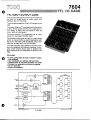
7604
TTL I/O Card
USER'S MANUAL
o
7604
TTL 1/0 Card
USER'S MANUAL
o
•
M-ffll~,I.FJm,
9/81
I
iii
Hi
.",.iWiTMIfII
P4iI4
H
+
FIlii H~
*'
I
14
-"Ii·
~
·F P"'''
4,.,
*.4, ..' ....',,4 """Nt :;;;::;:;:q
404
'" ~4; ,:;;p:.
.. ,I4W "w;:;""
,- rr',/Jl ~.. • •• ,
."
... ' *'
$ I<
&iIi·n ,.i\ii!\iii .. 4'" ,1$I, . ,W,iO!l!,
"U\!¢\_n•. ""~.e." .....£i, •• 2.,,.,_.E5( "_"., """",•• _ ••" .n H .•.J ..•. } .£ ..,.,.",.",".,.£,..• 3,. ___ "'"_. ___ ...•......•!E.2!!!1!~;_
o
o
o
o
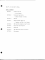
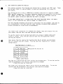
7604 TTL I/O CARD USER'S MANUAL
TABLE OF CONTENTS
SECll0N 1
Product Overview
- Block Diagram
SECTION 2
Functional Description
- General Purpose Interface
SECTION 3
Mapping
SECTION 4
Address Decoder Operation
- Changing the 7604 1 s Port Address
o
SECTION 5
7604 Card Environmental Specification
SECTION 6
Electrical Specifications
SECTION 7
Mechanical
SECTION 8
7604 Operating Subroutine Modules
SECTION 9
Maintenance
o
1 IT
IIA'I
o
o
o
o
~@@
.-
.r:',:,I~~~~~~~~TTL
7604
I/O CARD
TTL INPUT/OUTPUT CARD
This card provides 8 ports of which any number can
be input or output ports or output ports with
read back (64 I/O lines total).
.
The ports are accessed at 16-pin DIP sockets on the
card.
The output lines are TTL compatible with the ability
to drive 16 low power Schottky TTL Loads each (4
TTL loads). A reset line is available· to clear all
output ports simultaneously.
The input lines are TTL compatible with an input
rating of 4 low-power Schottky loads.
The ports are configure'd as input or output ports
simply by removing the unused Ie associated with
that port. If the input buffer is retained. output port
data may be read back into the Processor.
The 7604 decodes eight address lines with provisions for expansion and memory mapping, An oncard jumper system allows users to establish the
eight consecutive port addresses occupied by the
7604,
FEATURES
o
• 8 Ports conflgurable as Input or output or output
with readback
• User selectable port address (256 port field)
~ Outputs Drive 16 low-power Schottky TTL loads
~ Provision for expansion and memory mapping
, All ICts socketed
• Single +5V operation
DAT~~~ o--~-'---__i
IOCI~
0----<:1
'~T
~"T
KLICT
OICOOCII
"'0'
O------...J
w""C>---Q
AOO::!~ 0--7~--I
'---~
o.
I1'SIIUfT' C>---QII.W
:;>0--------------'
OUT~UT ~"TS
IMADtNG ,...o'CAns SOCatTl
JQ $
; aMliil\liiRffiiHfJ!<.$.!b.[,,&.:::B ,"",In;, "'i, M i~~ .!¢I'i,i"i\.lf".iiM, ".
fi'ii!ifl#'lfflffiWTIfTmE
I
·'ili i,R." i. Ii "
"NO'CATIS ACT'''' .OW LOG'C
• ¥IUS;:;;;
14
a; 4
"
I
11411444#44#4::;;:;;;::;44:;:;::: " ,,17. \
."jE, ;
g,,,
,M'.. I\!
*
#.." ..ifIW,."J¥It!, •
_1\I.U#6
~
q.
2.
FUNCTIONAL
The 7604 is shipped fully populated. The card is
customized (to A input and B output ports such that
A + B =8 ports) by removing the unused input buffer
or output port latch according to the following table.
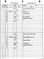
PORT NO.
Port
Port
Port
Port
Port
Port
Port
Port
OUTPUT PORTS
INPUT PORTS
IC NUMBER
IC NUMBER
U17
U19
U21
U23
U16
U18
U20
U22
U9
U11
U13
U15
U8
U10
U12
U14
0
1
2
3
4
5
6
7
o
Leaving the input butfer in at output ports allows the
Processor to read back the output port data to check
for noise alteration or to use the output port as a
data register.
The 7604 provides 64 alternating data and ground lines. These signal lines can be
up to 10 feet (3.0Sm) long with proper electrical considerations. When writing to
an eight bit output port the data bus data is latched in the output port. The
output data will remain latched in that state unti 1 it is written to with new data
or the SYSRESET* signal clears the port. When reading from an 8-bit input port the
of the port lines at the time of the read is transferred to the data bus.
RESET
The SYSRESET line clears all eight output ports to zero simultaneously. On,system
power-up the SYSRESET signal clears the output ports.
stat~
c=>
GENERAL PURPOSE INTERFACE
The 7604 is usefu 1 as a gene ra 1 purpose TTL interface ca rd. Iff 1at cab 1e or tw i sted
pair discrete wire cable assemblies are used, the ground-signal-ground of the I/O
connectors mfnimizes crosstalk between inter-system signal lines in electrically noisy
environments.
DATA BUI
-5V
BUFFER
q:7K
Qr--------t---<==~
r
OUTPUT STROBE
)
•
RESEr _ _ _ __
FROM
PORT·SELECT
OECOOERS
lH9UT ST-.o&. _ _- , . J t #....
FROU OTHER CIRCUITS
TYPICAL I/O CIRCUIT
FIGURE 2
74LS244
o
o
3.
Card Address Mapping
The 7604 Card is selected by a decoded
combination of address lines A3-A7. The user
chooses the card address combination by
connecting one jumper wire each from SX and SY to
pad matrices adjacent to U3 and U4 (see diagram).
The 7604 is shipped mapped at Hex Port Address 00.
To map the 7604 anywhere in the hexadecimal
add ress range 00 to FF, change the decoder outputs
connected to SX and SY.
Port Addresses
Address lines AO. A1 and A2 select one of eight Port
addresses. One input port and one output port
reside at each address. The RO- and WR- inputs
control the input gating and output latch functions.
~
o
ADDRESS DECODER OPERATION
Refer to the schematic, Document #104483.
The 7605 uses four cascaded 74LS4Z decoders (U3, U4, US and u6) to decode address
lines AO-A7. These decoders are enabled only when 10RQ* and 10EXP* are active.
Address lines AO, AI, AZ and the WR~~ signal are used to gate the select strobes
from u6 that control the output ports. Address lines AO, AI, A2 and the RD* signal
are used to gate the select strobes from U5 that control the input ports.
CHANGING THE 7604's PORT ADDRESS
Refer to the Assembly diagram, Document #104484.
Locate decoders U3 and u4 (74LS4Z) adjacent to the STD BUS edge connector.. Each
decoder device has a dual row of pads which form decoder output select matrices.
Make one (and only one) connection to each of the matrices adjacent to U3 and u4.
The decoder jumper pads numbered as shown in Figure 3 are adjacent to the decoder
chips on the 7604. Also shown are the jumpers (at XO and YO) which produce hexadecimal
port addresses 00, 01, OZthru 07, the selections made when the card is shipped.
Card Address Selection
o
FIGURE 3
imAA
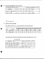
The I/O address mapping and jumper selection table for eight addresses per card
shows where to place jumper straps to obtain any eight sequential port addresses
in the hexadecimal range OO-FF. Using the lower of the 2-digit hexadecimal
addresses desired, find the most significant hexadecimal address digit along the
vertical axis, and the least significant hex digit on the horizontal axis. For
example, port addresses 00, ot, 02 thru 07 are obtained by connecting jumpers
at XO and YO.
o
The only restriction that applies in address selection for the 7604 is that the
lower of the eight port addresses (00 as shipped) must occur only at every eighth
possible address; for example, the sequence 01, 02, 03 thru 08 is not allowed by
the decoder.
The pad matrices adjacent to U3 and U4 are on 0.10 inch (0.25cm) centers. The
jumper wires may be conveniently replaced by wi rewrap post if frequent address
selection changes are anticipated.
MOST
SIGNIFICANT
HEX AODR£SS
LEAST SIGNIFlc.un' HEX ADDRESS
o
I I 21 3 T
1
4f 5
I •I
7
JUMptA
xo
xo
0
xo
YO
1
XO
Y2
2
Xl
YO
Xl
'1'1
3
4
5
X1
'1'2
Xl
'1'3
X2
YO
X2
'1'1
X2
'1'2
x2
'1'3
•
•
Y1
'1'3
X3
yo
X3
'1'1
7
X3
'1'2
)(3
Y3
X~
YO
X~
'1'1
t
U
'1'2
X~
(3
A
xs yo
xs '1'2
x6 yo
xs
Vl
)(5
Y3
XI;
Y1
8
C
0
E
F
x6
X7
SELECTION
'Tt1Af,fClo1E1F
'1'2
)(6
Y3
YO
,,7
.",
XT Y'l
)(7
Y3
1"\
x
AND
Y
o
l/
I/O Address Mapping And Jumper Selection Tables For 8 Addresses Per Card
FIGURE 4
o
~----~------------------
o
50
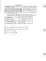
7604 CARD ENVIRONMENTAL SPECIFICATIONS
R£COMMENDED OPERATINb LIM I TS
PARAMETER
MIN
Free Ai r TemperatIJre
Humidity
CD
ABSOLUTE
TY?
MAX
25
55
0
CD
J
5
95
~ON-OPERAT'N' LIMITS
MAX
UNITS
-~O
75
°c
0
95
%AH
MIN
Non-condens i n9
,. ELECTRICAL SPECIFICATIONS
7604 GENERAL PURPOSE TTL I/O CARD ELECTRICAL TEST SPECIFICATION
o
RECOMMENDED OPERATING LIMITS
MNEM.
PARAMETER
ABSOLUTE NON-OPERATING LIMITS
MIN.
TYP.
MAX.
MIN.
MAX.
UNIT
Vee
Suppl,y voltage
4.75
5.00
5.25
0.0
7.00
Volt
TA
Free air temp.
0
25
5S
-40
75
°c
USER WORST CASE ELECTRICAL
CHAR~CTERISTICS
OVER RECOMMENDED TEST LIMITS
For Input Port
&
MIN
High level input vo 1tage
Low 1eve 1 input voltage
Hysteresis (VT+ - VT-)
2.0
PARAMETER
VIH
VIL
0.2
TYP
MAX
UNIT
0.7
V
V
0.4
for Input current each port 1ine represents 4 LSTIL loads
V
-
o
z, ##
c.
ii4iiiiLtiMJMlliii;"!),ijmNWIlilDUd$&4%IfifIflfl9IDi\'HiOOiibfiMM_=iWiKMit,,,aaa&iiZMUiiBJWi
M '.
liP",; ¢
4
&(7
4
4iMIL4IIN"'" "I
44QEZ#4ZZA,*
4M
For Output Port
PARAMETER
-&
MAX
UNIT
0.5
V
V
* 1 LSTTL load - O.4mA
STD BUS ELECTRICAL CHARACTERISTICS OVER RECOMMENDED TEST
ll~ITS
High l~vel output voltage .&
VOH
low level output voltaQe
VOL
Each output can drive 16 lSTTl loads*
MIN
TYP
2.7
3.5
0.35
A
o
,
t
MIN
PARAMETER
ICC
SUPPLY CURRENT
TYP
MAX
450
700
STO BUS INPUT LOAD
See Figure
STD BUS OUTPUT DRIVE
See Figure
UNITS
rnA
6
6
~ Input characteristics with output chip removed.
&
Output characteristics wi th input chip installed.
~ Vee = 4.5V
IOl
= 4.5V
IOH
A
Vee
= 8mA
= 400).tA
0
J
"
o
o
I
7.
MECHANICAL
· Meets all STO BUS general mechanical specifications
· May require one additional card slot width for ribbon
cable access to ports (connector dependent).
· Connectors use low profile l6-pin DIP plugs with heavy
duty pins. T and B Ansley Catalog No. 609-M165H or equivalent.
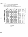
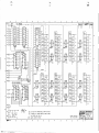
mmI
r
mEl
U1
74l.S244
U16
74L5273
I~
U2
74L5244
U9
74LS244
10
U17
74LS273
Ul0
74LS244
U1I
74LS2n
'0
un
74LS244
.e
U19
74LS273
10
r
I
I
I
U12
C
U20
74LS244
74LS273
U13
745244
U21
L....J
10
••
~
74L5273
'0
U22
..
74LS273
UlS
74LS244
~
7604 ASSEMBLY
5
•
dlil·",;;y,
"lfiltit!i f'\.
4iAN;:M
MijhNh
1,;Hj'i"'I\!~"'''"il\ii!hi¥\fl¥Hi4,w¥',
>-
en
en
c
~:: ;.;;: :~I
FIGURE
••
IPf4f,M' ',i1h4¥
T
,1,.1.19\
L
,i ,II
PORT
BIT
o
1
2
3
4
5
6
7
Input/Output Port Socket
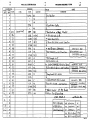
STDI7604 EDGE CONNECTOR PIN LIST
PIN NUMBER
PIN NUMBER
OUTPUT (DRIVE)
OUTPUT (DRIVE)
INPUT (LOADING)
INPUT (LOADING)
MNEMONIC
+5 VOLTS
GROUND
-5V
MNEMONIC
1
2
4
VCC
GNO
3
6
07
1
60
06
60
05
1
1
04
1
60
5
7
8
10
12
14
60
VCC +5 VOLTS
GNO GROUND
-5V
60
1
1
03
02
01
9
11
60
60
1
13
60
1
DO
1
A7
1
A6
1
1
A5
A4
A15
16
A14
18
15
17
A13
20
19
A12
22
21
All
24
23
1
A3
Al0
26
2
A2
A9
28
25
27
A8
30
29
2
2
1
AO
WR'
RO'
MEMRO'
1
32
31
34
33
1
1
A1
lORa'
MEMEX'
36
35
MCSYNC'
STATUS 0'
38
37
REFRESH"
39
41
STATUS l'
BUSRO'
40
42
INTRa'
44
43
IOEXP'
BUSAK'
INTAK'
NMIRO'
46
45
PBAESEr
48
47
CNTAl'
50
49
CLOCK'
PCI
WAITAO'
1
SYSAESer
52
51 OUT
PCO
AUX GNO
54
AUX GNQ
AUX-V
56
53
55
IN
AUX ·V
"DeSIgnates ActIve low Level logIc
Edge Connector Pin List
FIGURE
6
• Address. Data and Control Busses meet all STD
BUS general electrical specifications except AO.
A 1 and A2 which are 2 LSTTL loads each,
o
•
8.
7604 OPERATING SUBROUTINE MODULES
This section provides flow diagrams and subroutines to operate your 7604 card.
may be used intact, or used as models to construct subroutines for a specific
These
ap~lication.
The subroutines are written in 8080-fami1y assembly code and wi 11 execute on 8080,
8085, and z80 processors. The memory addresses selected are compatible with Pro-Log's
7801 (808SA) and 7803 (Z80) processor cards. The 7604 port addresses used are
the address jumper selections made when the 7604 is shipped.
To use these subroutines in systems other than those described above, the
andlor lID port addresses may require change for compatibility.
~emory
The flow diagrams presented can be easily translated into the assembly code used by
any microprocessor since they show the steps required to achieve 76d4 operation
without reference to a particular microprocessor.
The (check bits) subroutine wi 11 compare the present input port status with the
port status from the last time that the port was read.
To use the routine the HL pointer must point to a place in memory where port
status is stored. Also, the port must be read into the accumulator before
calling the routine.
o
Upon return from the routine the location that the HL pointer was previously
set wi 11 contain new port status. Plus the next four locations will contain
change status.
Uses Registers A, Hand L
1
M
M+l
H+2
M+3
M+4
I
XX
XX
XX
Old Data
xx
Bits to Zerc
XX
Bits to One
New Data
+-Location HL was set to
Changes
Memory after Return
The (set bit) routine can set a bit or bits on an output port.
load the accumulator with the bits that should be changed.
(Input chip must be installed)
To use the routine
The (clear bit) routine can clear a bit or bits on an output port.
routine load the accumulator with the bits that should be changed.
(Input chip must be installed)
•
;L Mij iG&M\IiiIWWi&M1
'"
To use the
~
I
CHECK BITS
L
SAVE 8 & C
.L
LOAD B WITH
OLD DATA
1
EXCLUSIVE "OR"
OLD DATA WitH
NEW DATE
l
STORE BITS
ITHAT CHANGED
_t
"AND" OLD DATA
WITH CHANGES
~
STORE BITS THAT
TO ZERO
~ENT
.~
"ANO" OLD DATA*
WITH CHANGES
~
STORE BITS THAT
WENT TO ONE
~
RES10RE B & C
~
RETURN
)
•
SET BITS
.It
INPUT PRESENT
STATUS
, II
"OR" IN
NEW BITS
,~
OUTPUT NEW
STATUS
~iI
C
o
RETURN
CCLEAR BITS
""
INPUT PRESENT
STATUS
~Ir
MASK OFF
UNWANTED BITS
OUTPUT NEW
STATUS
,If
•
RETURN
)
o
,~
~
PRO·lOG CORPORATION
~.[XADECIMAL
PAGE
LINE
AOR
ADA
MNEMONIC
INSTR
LABEL
0
LOPI:.
-
1
2
-
3
IrA
..
~
~
v "
,
~
'XX
•
Be
77
SIAN
13
i"y
8
Itt=>
m
9
70
AS
ST8N
(ttL)
XRA
'( P
B
l-lL
(fH.)
B
23
c
0
77
4F
E
7B
F
At
23
<;tA~
LDC
LoA
ANA
1
77
\ ( F'
<; rAtJ
2
78
LDA
3
2F
Al
eM"
5
2~
6
77
A~&
\CP
l-\L
7
C.I
8
CCj
RTS
UN
o,,{ ..
of- OLO
-r-
fH tJfW ~
--
CH~~GES
0000_1.111 o&. D
@ 0'010101 _NM.
r- S'on' (~A"'6r~ '&11 ft.Jr')( ~ I at"_f. t i • .,
-4- PtA
CI,.Q.,G\C!s i ~ C
... f\,f o~a OATh
~
::.
t..,
A
OLD ~ C"AtJ~E5:: e;~sJQ~erO.
S~Ot. 8;+s J 0 '2tt.t! ;tf\ l) ....d Loc..J."on
0000' ,.,
• 01 0 11010
ODCO '0 10
1
-
OLD
J-
C~A~6ts ~
s~t, ~L1 :?£ro I
~
•
--OffieCHAtJGES=
]:~'Dff' B.~':. ~~ OIJ~
tat
~o ONE.
III, oDCO
.. CJ, 0'
; .. turKt locc>l;Dh
J
f-
---
t·
-~ {Atfttlirr1tnl OLD l}AfA
..
.-
C H... ~C.£ $
() l(H ,0' 0
1
f Cd D
JUJo ~
. . ee~
Ut""-
"f t,~
hor'r\'C. .L"'''oJ+ine.
Co,.,4~,.c,
\.J S£~ ~e~*
l~~_C
s.ts ~
I
awJ Po, nn~
A
~
~A M ~1EP-1o ~ V
1/~(rrR e,.~ UT '-1
0
I(USES
'"
5lCJC~to\l\!;\,
"OLD
t.t-\ At-JGES
() '010000
C
F
-
S~ ~reOLD I)~ ~~i.JIl ~~ I.ft~'C ~~O~
9
E
I .... J c
~
~
STAtJ (Hl)
PLP
Be
-
~Ir
{HL)
L
At.,
--OLD ~~A J~ B
f- C;fote tV~vl
A
B
L
B
+- PV+
~~
t-
l)
LHL
D.J.o.
... ~~ u,J""(!I" ri
7
r
-...J
. ~I~~
, New
M[~&J.
B
-........ ......
lr--..h\
~
lDB
A
f)~
x~
4b
~
)-")
.~
8
.
f.'..
psp
;:. ~~.f- 1>n \ h~er
III
CS'
0
<)
-
COMMENTS
MODIFIER
5
A
...........
«t..d \1 ....1
-
DATE
TITLE
INSTR.
o
PROORAM ASSEMBLY FORM
-
~~E'" ~"A
-
f.( L
,
=
M
)r.)(
OLl) £)I\'tA
M'4 1
J(K
Cl\I\~6(S
tv1.f 2
)(_~ _B;1 ~ \!) Uffi
~~ Jl:\~-i[)D'JI
ONE
1"1".1
M-4&./
I0GCI01
,m
•
HEXADECIMAL
LINE
PAGE
INSTR.
ADA
ADA
MNEMONIC
LABEL
-
1
(Se~
2
4_1
3
DB
4
xx
-
60
0_3
ORA
OPA
6
7
xx
8
_Cl
BIT)
LOB
IPA
-
R,S
PROGRAM ASSEMBLY FORM
7 b 0'-/
TITLE
INSTR.
DATE
MODIFIER
COMMENTS
-~ LOAd A w:.\~ R.]{s) ~Db~ ~±
LD~r
0
5
o
PRO-LOG CORPORATION
)()(
A
~
4-54v~ Bas ih
I-~ IhDvI- Por-l- 9-0\.+ \1<"
I
xx
B
'-OR ~h l\)bJBi ....S
.;:.. out~
tJe.W
,
~
B
J:b,+
S-l-Q.lvs
1r
9
A
B
C
D
E
F
1
~
2
2f
3
47
4
DB
5
~X
6
AO
03
7
(\'
8
~"
9
C"-.....
\}
~
\
~
,.....
B
C
D
(
~) ~
,
A
.....
~t:
E
F
-~ W
l-DAr
0
xx
Cq
("etA" ~; f)..
-
XX
CMA
LOS
t-
IPA
-
XX
-
)()(
ANA
OPh
~T~
B
be.
cJ~ ar e d
,
-r-
A
A tA/;fh &;+ (s) fa
~l~ ..... if
(0.,...01;
, Wl~n+ 8i
Mi~&
r
-;: -r~ nuf Ib r.J. ~~4tv S
,. I
~ Ma~k ty{f B;.J.~
-~ OufD~
, ~ {trt
,
StOtfus.
•
.~
f-~
'"".,/
\_~
1415 ~~
SY$I/E'
.r
BUFFERS
BUS
~~~T*
h
Col>
I
I
os
04
03
D2
1)1
00
_1
~
~
\
/
\
/
~
74/.S;44
SIlO'
"V-
1 IIns
II
(lYP)
/
2
1101
'5
..
8
" f - - - J 1103
Z
~
..
9
UI
" -f{"
I
I
I
,.
.8
14l5l44~
(lYP)
~
r;;- ~
1415244
ClOD
,.
II
E2' E21
1T~
I
I
['---!!-
I
~
I
~
t
[::::.~
\
I
12
'OS7p!-o
J4l~2
m
A1
A&.
\
I
"
C
\
'4
B
I
5(.
p.:-o
~'0S7~
741542
1
U4
'5s~
"
52
p.l-o
51
p.L-o
~8
'5 A
A4
Will
IIOt
p1.
1'--2-
,
,
~&SY
\
/
-
\
V- r---
I
1'3
~~
~0'S7~
I5t._
14L542
1
1J5S1n~
I~c.
ss~
S4~
1411
s,~
52~
"11
'll~
~~
II
~1iST~
14154~
~c
--'!.p,
ut..
1 05&.a
~
,,>s~
S4~
/1A SI ~
~~
"
0-2
~,+
0·1
gJ tI I CZ~l
~o ;RJ I':~~ I
CI
0.1 UF.
"
8
~N/I'.
J5V
~m
&
&
1.
NorES:
f-<II
I.
5
TIOt·O
~
tm
l'S
2-'
~IZ
1/.,-"
".
k"/ J
2-'
tj}y
2-2
f-<'.
R"-5
<2
2-'
II
f-<15
RII·"
/ , I/O
OSH
1/
y
l-t.
Zoo
8
I
/I
V
t-<'"
,
RSTlt
O~1
7
R8-.
R,-.
./~
tID
4-5
8
f-<II
4-4-
R'-l
4·,
,
4-2
./2
00
/I
V
f-<'"
IISTll
11
r.
t
01.-.:,
I
(.-5
~.+
'2
(.-'
"
,.
(.-2
,1
O~1
8
4·1
K'5
IllO 4-0
054t
~
f-<,3
f-<14
1/8-2 ""
IN
UI.'
f-<,z
4
RI-'
4-"
f-<'O
S
R8-3
~
1<'
I
05".
RiT.
(.-/
15
1 Clo 01.:0
",
I
( TYPICAL)
- -
-
R4-'l
RIO-"
J
8
r<'
./7
~~
./11
f-<'2
/4
RIO'5
K"
RIO-4
I-I.
Rl-t. "
1-5
<3
rrr
'-4
8
I~
117'S
'I
ls,·B"
r-..
..
1·2
./2
1-'
f-<15
' liD 1-1'
k't.
Rsr.
'-t.
'--<'0
/,.
R"-5
~-s
S
RH-4
I----{I3
"3
111-3
I----{I.
2
3-4
'-3
'-2
"
/ , liD
'H-J
IN
lS5»
_R,t/
RIO-2
Iq
Rt-2
~Y
BOUT
,-,
L<'~
/I/i-'
~~
"
I----{ 12
111-4
4
~..",:T,'
j1
/1/0-3
>--{"
H
~,
/11 rJ!> '-1
r<'7
RH-"
Ullj
~"
R'i-t.
R~-5
~
Ri'4
+sv
./5
,
,
"
'·0
f-<'"
•
055'
,:
i
,
Rsre
119-6
112-1.
5-"
7-~
H1
I----{IO
r.
~
8
-5
./5
~-
4
IS7-
I----{12
..
IN
1
>--<"
f.
yryl'
3
[-<,,.
1-S
G,
7-4
'2
'7·'
"
S-2
f-(14
f-<15
./, flO
10
5- 3
I----{ "
2
/19'5
8 IIO 7-7
/8 TID 5-7
r<"7
S"
s-o
7-1
~" ~:;,
l:JP
I.
7-1
15
I
ClO
7-0
-(It.
1
sx snEC.~
I Gf- II ADORES5 IIIlJCI(S,
SY ";ElE<l'S I Of- 4
IIll ReSISTOR
IlNl£'5S
J
1'1
· D:T,'
~IS
I
lm-l
RII-"
./
m®-J
II1!t'!!'
0-3
k~
8
Z
/
RI.-l
~'7
!I [/0
8 I/O 4-7
R,-5
I
R5T.
tW
~
IN
152. I
•
,
"
I
PCO®.
0-4-
K'"
I
II
our
as'.
5
8
-<8 110 '·1
U"
8
0-5
"
M~
'i2~
/7
R4-'
IN
IS'.
"
t-"<'./35
RI·"
t:Jr.r
lUH2
PORT SHEa DEWOER5
Rl-3
~,z
11'-3
!l. Ul):1.!..
\
R'-3
~II
./2
r<'
0-1.
~/O
'R1-2
R8-S
/I rIo 2-7
RI2-~
~
OSO.
Z 741532
J
AO
""FJ:
Rsrlt
/
A'
f!!-/
OUT
~
Rr.-'
8 rID 0-7
R2-.
R~-1
f2-/
7'l5213
I-
- - - - -
L
'/
At
r--
r-0
~
r-~
~
r-~
~
I~
iJ!!.J
r-~
~
t
rLo
r<'
./7
['--!-
I
so~
'---- &SX
Ai
SI
~
t
I
53~
S2~
~
119-4
~ r-;.;- f.L/
I
,
'5(.1>-'$S ~
'54
S3~
:;o~
IIlIlQI
C.
S4~
15 A
AS
1
I
rso,n;~
I
II'Exr,
f-L-/
~
I
~
I
Rl-5
P
P
0
f'--2-
I
CI1RD SELECT DECODERS
IN
I~
I
Tf;"
(lYP)
I
fSV
~y~
I
~
~
II
~74l5244-~
~
~
Fi
I
I
I
.r-->
r-;:;;-
12
I
~-f1>- r------
7 liD'
,
(rv,,)
r-;;-
~y
1104
'5 14l""
~
3
~
~
AUUtts,,>
Vl\lIJ1'S
orIlERWI~E
ME
n
Bl.OC/CS, fI
4.1 It.
SPEC.I"IED.
FORT';
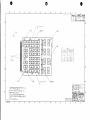
PRO-LOG CORPORATION
~~~~j.:5
PER BlOll.
POlUS PER 8lOC.lt.
ASSfMI')lY NO. '04464
'AR7S l/"lT NO. '04485
•
•
o
8
7
6
5
4
2
3
/\lI"f fl III M .", Ann, f)
~'~I\~ ~'
I, II ~l I: ~\I.~;.
'I
l'rN H,.,")
~L ~~V'~!{) P~I!.. ft:N QB~8
I~
\
'I
r''''
I ... ·." ..
D.
.D
- IN.'\lT
t'{lR I') 11M "III',
~
201 III ~fa.
12
(~,<"
\ .l..t \
Hr,\!]
.l.
~
I.
r:~~;:]
C
rdh] [:;§;J
(5)-
~gggggggu
------
~
[:7~~:~
___ ,___
L'l
,I
t
Aiir
,
fAil
A
0000
~OOOSY
.21_
r:~~;~
~:: ~~~~:]
c
TABL[ 1
Hllt,r
INI)1I1 l't>lH:1 Nn
r:;;;:) r:::EJ
--~-----
-
I Air II
141',.'/'
-------~-.---
1117
IJI')
?
-.---------
,~"--
r:~;;:] r:7~;;:]
r
':
ur.11 RI2
r:~.;.~;:]
17101
1/1
:'
1110
112?
I
0
o ••
n"~ 1:1'~'lj
B
H
:II.
o
o
mmI
18
0
: 110
o
o
11,'\
.--.L, ~,~±~___ ~~,'_- ---
"T'H H
o
o
t::~;;:) :~
r:~;;:] lC~
B
RfWIVI r Hllr liT
..
()
J
"
I~I Ie KEG!.
I'()HI'> lIfb-un
It-::.
:~
~
A
R.< DfS/GNATlONS A~ Foil. lO(AIIN& 1"U~IlOSES ONLY
MAY NOT API'{ A~ ON ACTUAL rM. T
~
IOfNTIH "'II"
&
OENDreS
~SY
Rev LeITER Lr.>/N6
PI~IIO 10.
~Uf\f\ER
TI)
I,
)~r'I(,"Hf
ITEM OESCRIPTION
A', INflll1 I'()H I <., HfM()Vf
Will N 11:>1 [) A', AN OIlTf"IIT
!l\MIII"'ID 11)1'111(1 ()O,
741944, MAV
ASIDD4
f(,
prJ{
fir ,rfT
8
~~~:,.:+:.~~_i
'
SCHEMATIC NO,
I(),"B~
PAR'I'S U":>T NO, 104485
7
1RI
'RI3
REF OESIGNATION
PRO-LOG CORPORATION
TAAII J.
'N,
N, \I f',: '",' I',', (" HI PINI',I "l'rUffln
uu~~;~!:;
NHWOI1K
'1 .. , , - - - - - - - - - - - &,
104~S2---- 'PWB..
IA
!,TAMP
IC:S (ryp)
tlOIIRD ro CDYFOIi:M "IIH ASSY PIi:OCEDuRES
.3
A
14 ,7K
+~-:F!. ~: - ~~::~----- . .-
AUD
6
5
4
3
2
o
()
--.~----~-'-'--.-'--'-'
~~
•
•
•
$I; Ii SiAi_aSStZaS.SiU:::,
ii;
4 XI t I lUi
Ai $I "iid
iE
o
o
USER'S MANUAL
2411 Garden Road
Monterey, California 93940
Telephone: (408) 372-4593
TWX: 910-360-7082
'0
1066658
600
9/81