1
3: INTERFACING TO THE MOTOROLA MCF5307 “COLDFIRE” MICROPROCESSOR
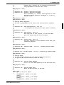
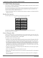
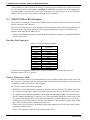
Generic #1 Interface Mode
Generic #1 interface mode is the most general and least processor-specific interface mode on the
S1D13705. The Generic # 1 interface mode was chosen for this interface due to the simplicity of its
timing.
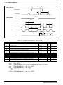
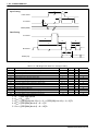
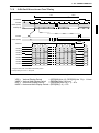
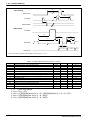
The interface requires the following signals:
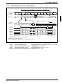
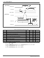
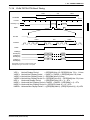
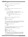
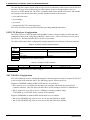
• BUSCLK is a clock input which is required by the S1D13705 host interface. It is separate from
the input clock (CLKI) and is typically driven by the host CPU system clock.
• The address inputs AB0 through AB16, and the data bus DB0 through DB15, connect directly to
the CPU address and data bus, respectively. On 32-bit big endian architectures such as the Power
PC, the data bus would connect to the high-order data lines; on little endian hosts, or 16-bit big
endian hosts, they would connect to the low-order data lines. The hardware engineer must ensure
that CNF3 selects the proper endian mode upon reset.
• Chip Select (CS#) is driven by decoding the high-order address lines to select the proper register
and memory address space.
• WE0# and WE1# are write enables for the low-order and high-order bytes, respectively, to be
driven low when the host CPU is writing data to the S1D13705.
• RD# and RD/WR# are read enables for the low-order and high-order bytes, respectively, to be
driven low when the host CPU is reading data from the S1D13705.
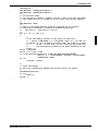
• WAIT# is a signal output from the S1D13705 that indicates the host CPU must wait until data is
ready (read cycle) or accepted (write cycle) on the host bus. Since host CPU accesses to the
S1D13705 may occur asynchronously to the display update, it is possible that contention may
occur in accessing the S1D13705 internal registers and/or refresh memory. The WAIT# line
resolves these contentions by forcing the host to wait until the resource arbitration is complete.
This signal is active low and may need to be inverted if the host CPU wait state signal is active
high.
• The Bus Status (BS#) signal is not used in the bus interface for Generic #1 mode. However, BS# is
used to configure the S1D13705 for Generic #1 mode and should be tied low (connected to GND).
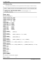
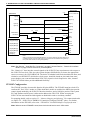
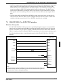
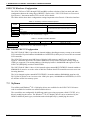
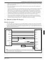
3.4 MCF5307 To S1D13705 Interface
Hardware Description
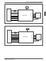
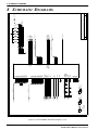
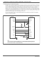
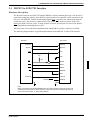
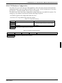
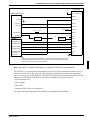
The S1D13705 is interfaced to the MCF5307 with a minimal amount of glue logic. One inverter is
required to change the polarity of the WAIT# signal, which is an active low signal to insert wait
states in the bus cycle, while the MCF5307’s Transfer Acknowledge signal (TA) is an active low
signal to end the current bus cycle. The inverter is enabled by CS# so that TA is not driven by the
S1D13705 during non-S1D13705 bus cycles. A single resistor is used to speed up the rise time of
the WAIT# (TA) signal when terminating the bus cycle.
S1D13705F00A APPLICATION NOTES
(X27A-G-011-01)
EPSON
5-21