1
CHAPTER 1 SYNCHRONOUS DRAM
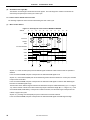
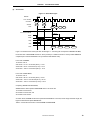
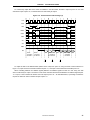
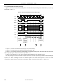
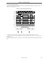
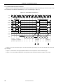
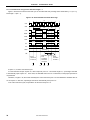
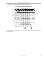
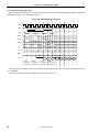
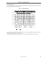
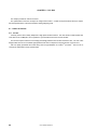
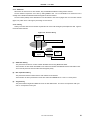
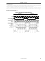
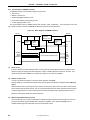
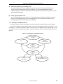
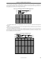
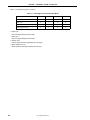
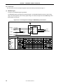
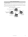
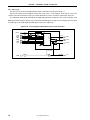
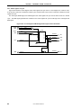
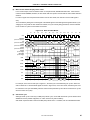
If a controller that generates the following signals is designed, the conventional DRAM and SDRAM can
simultaneously be used.
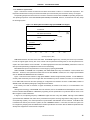
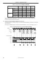
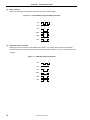
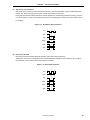
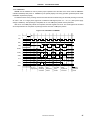
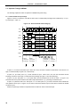
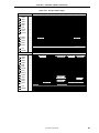
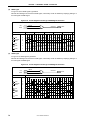
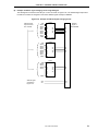
Table 1-4. Correspondence of Control Signals of Conventional DRAM and SDRAM
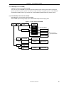
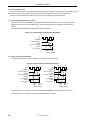
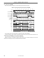
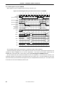
Figure 1-6
Conventional DRAM
SDRAM
<1>
RAS# signal is active
Input active command
<2>
CAS# signal is active
Input read command
<3>
RAS# signal is inactive
Input precharge command
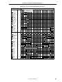
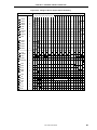
1.3 Control Method of SDRAM
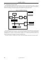
The following explains control methods commonly used, taking 16-M SDRAM as an example. For the detailed
control method of SDRAM, refer to the user's manual of SDRAM.
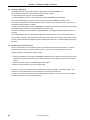
1.3.1 Pin functions
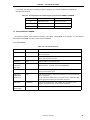
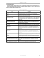
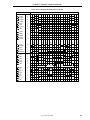
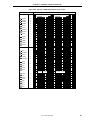
Table 1-5. List of Pin Functions
Pin Name
Input/Output
Pin Function
CLK (Input)
Input
CLK is the master clock input pin. Control signals of SDRAM are referenced to
the CLK rising edge.
CKE (Input)
Input
CKE determines validity of the next CLK. If CKE is high, the next CLK rising
edge is valid; otherwise it is invalid.
CS# (Input)
Input
CS# low starts the command input cycle.
RAS# (Input),
CAS# (Input),
WE# (Input)
Input
RAS#, CAS#, and WE# have the same symbols on conventional DRAM but
different functions. For details, refer to 1.3.2 Commands.
A0 to A11 (Input)
Input
A0 to A11 are address input pins. A10 defines the precharge mode. A11 is
used for the bank select signal.
DQM (Input),
UDQM (Input),
LDQM (Input)
Input
DQM controls I/O buffers. DQM high and DQM low turn the output buffers off
and on, respectively.
×16-bit products are capable of byte control (8-bit control). UDQM and LDQM
control upper byte and lower byte input buffers, respectively
DQ0 to DQn
Input/Output
DQ0 to DQn are data I/O pins. DQn are DQ3, DQ7, and DQ15 in ×4-bit
products, ×8-bit products, and ×16-bit products, respectively.
VCC, VSS
(Power supply)
Input
VCC and VSS are power supply pins for internal circuits.
User’s Manual E0124N10
21