1
S3C825A/P825A
UART
UART MODE 0 FUNCTION DESCRIPTION
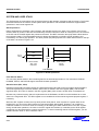
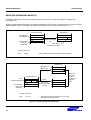
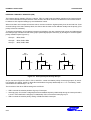
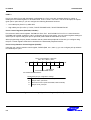
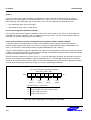
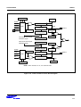
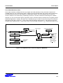
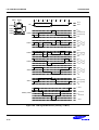
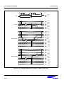
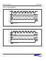
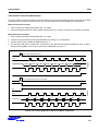
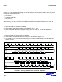
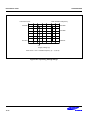
In mode 0, UART is input and output through the RxD (P5.4) pin and TxD (P5.5) pin outputs the shift clock. Data
is transmitted or received in 8-bit units only. The LSB of the 8-bit value is transmitted (or received) first.
Mode 0 Transmit Procedure
1. Select mode 0 by setting UARTCON.6 and .7 to "00B".
2. Write transmission data to the shift register UDATA (F9H, set 1, bank 0) to start the transmission operation.
Mode 0 Receive Procedure
1. Select mode 0 by setting UARTCON.6 and .7 to "00B".
2. Clear the receive interrupt pending bit (INTPND.5) by writing a "0" to INTPND.5.
3. Set the UART receive enable bit (UARTCON.4) to "1".
4. The shift clock will now be output to the TxD (P5.5) pin and will read the data at the RxD (P5.4) pin. A UART
receive interrupt (IRQ3, vector D4H) occurs when UARTCON.1 is set to "1".
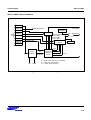
Write to Shift Register (UDATA)
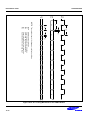
RxD (Data Out)
D0
D1
D2
D3
D4
D5
D6
Transmit
Shift
D7
TxD (Shift Clock)
TIP
Write to UARTPND (Clear RIP and set RE)
RIP
Receive
RE
Shift
D0
RxD (Data In)
D1
D2
D3
D4
D5
D6
D7
TxD (Shift Clock)
1
2
3
4
5
6
7
8
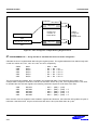
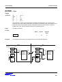
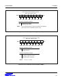
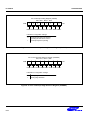
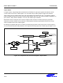
Figure 18-6. Timing Diagram for Serial Port Mode 0 Operation
18-7