1
S3C825A/P825A
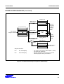
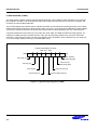
TIMER 1
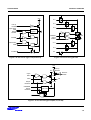
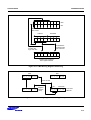
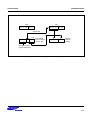
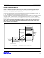
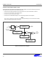
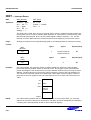
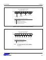
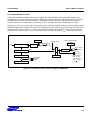
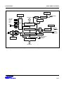
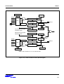
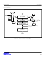
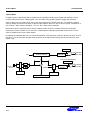
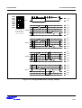
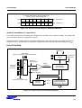
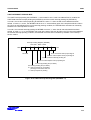
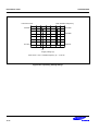
BLOCK DIAGRAM
Bit 6, 5, 4
Data Bus
8
T1CLK
fxx/256
fxx/64
Bit 3
16-Bit Up-Counter Clear
(Read Only)
<TBCNT/TACNT>
MSB
LSB
MUX
fxx/8
fxx/1
16-Bit Comparator
Match
Pending
Bit 0
Bit 2
Bit 1
Timer 1 Buffer
Register (16-bit)
T1INT
IRQ1
TAOUT
Counter Clear Signal
Match Signal
16
Timer 1 Data Register
(Read/Write)
<TBDATA/TADATA>
MSB
LSB
NOTE:
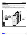
When TACON.7 is "1", 16-bit timer 1.
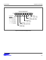
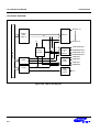
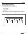
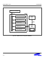
Figure 11-2. Timer 1 Functional Block Diagram
11-3