1
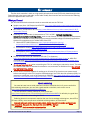
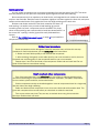
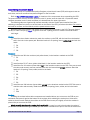
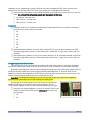
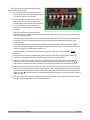
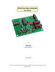
Assembling the FCC4 Fast Clock Controller Kit (Excerpted from the FCC4 User Manual) by Mike Dodd [email protected] April 13, 2014 This manual and the firmware programmed into the microprocessor are copyright © 2014 Michael M. Dodd All rights reserved KIT ASSEMBLY The fast clock controller is built on a high-quality printed circuit board (PCB) with plated-through holes. Plated-through holes have metal walls, so the solder readily flows into the hole and out onto the soldering pad on the opposite side of the PCB. What you'll need you will need these basic electronics tools to assemble and test the FCC4 kit. Needle nose pliers. (All Electronincs #PLR-55 http://www.allelectronics.com/make-a-store/item/plr55/5-mini-long-nose-pliers/1.html). Wire cutters, (All Electronics #FC-14 http://www.allelectronics.com/make-a-store/item/fc-14/5flush-cutter/1.html). Soldering iron, 30-45 watts, tip temperature of 700° to 800°. I strongly recommend a temperature-controlled soldering station, such as one of these. You can adjust the tip temperature, and the tip is isolated from the power plug to prevent household voltage from destroying sensitive electronics components as you solder them to the PCB. Weller WTCPT (HMC Electronics: http://www.hmcelectronics.com/cgibin/scripts/product/1980-0217/?gclid=CPaA2vaMuZ4CFchn5QodJ2l0pg). All Electronics IR-361 (http://www.allelectronics.com/make-a-store/item/ir-361/60wtemperature-controlled-solder-station/1.html). All Electronics IR-50 (http://www.allelectronics.com/make-a-store/item/ir-50/temperaturecontrolled-solder-station-50w/1.html). 60/40 rosin-core solder (All Electronics #TS-110 (7' in dispenser) http://www.allelectronics.com/make-a-store/item/ts-110/60/40-solder/1.html or #SOL-564 (½-pound spool http://www.allelectronics.com/make-a-store/item/sol-564/60/40-solder-1mm1/2-lb-roll/1.html). Do not use flux of any kind when assembling the FCC4 or soldering any electronics circuit. The rosincore solder listed above is intended for electronics use, and needs no additional flux. You will void your warranty if you use flux. You will need a voltmeter capable of reading up to 10 volts DC to check-out your power supply before connecting it to the FCC4, and for troubleshooting if the FCC4 does not operate properly. An inexpensive multimeter such as All Electronics # DVM-810 http://www.allelectronics.com/make-astore/item/dvm-810/economy-digital-multimeter/1.html is suitable. About soldering You need to know how to solder electronic circuits to assemble the kit. If you are unfamiliar with soldering techniques, you can find a good tutorial on the Web, such as this one at http://www.aaroncake.net/electronics/solder.htm You can purchase a solder practice kit, such as this one: http://www.makershed.com/ProductDetails.asp?ProductCode=MKEL2 It definitely is a good idea to hone your skills before assembling the FCC4. Soldering electronic components requires the use of a low-wattage soldering iron, about 35 to 45 watts. Ideally, use a temperature-controlled soldering station, as listed above. Use only rosin-core solder on electronic circuits. Never use acid-core solder, and never use flux of any kind. Not paste flux. Not liquid flux. Not rosin flux. No flux! Remember: Rosin-core solder only and no flux. FCC4 Fast Clock Controller User Manual Page 1 Getting started You may solder components such as resistors and diodes from the front side of the PCB. This eases assembly because you can press the component against against the PCB while soldering. Some components such as capacitors, terminal blocks, and integrated circuit sockets can be soldered only from the back side. Bend the leads of capacitors slightly to hold them against the front side, and press sockets and terminal blocks firmly against the front side while soldering on the back side. Resistors and diodes used on the fast clock controller PCB have 0.4” hole spacing. It is helpful to buy or make a lead-bending jig to avoid measuring each time such a component must be installed. This photo shows a commercial jig and a resistor with its leads bent downward 90° at the correct 0.4” spacing. A similar jig could be easily fabricated from styrene. Refer to Fig. 2: FCC4 Component Layout. on page 3 as you install the components in each step. Fig. 1: Component lead-bending jig. Solder/cool procedure Some components can be damaged or ruined by excessive heat, so follow this two-step procedure for each lead wherever you see solder/cool in the instructions. 1. Solder one lead. Solder quickly to not overheat the component. 2. After soldering, blow gently on the solder joint for one or two seconds to cool it, then turn the board over and blow gently on the component itself for one or two seconds. Repeat steps 1 and 2 for each lead on the component. Solder and cool each lead. Do not solder all the leads at once without cooling. Don't overheat other components Even if the instructions don't say solder/cool, you can employ a soldering technique that minimizes heat damage to components such as resistors, capacitors, and plastic components such as sockets, plastic switches, and terminal blocks. Similar components usually are installed together. Insert all components listed in a single step into their holes, then begin soldering. Solder one lead one each component in turn, then come back and solder another lead. This gives each component time to cool before you come back to solder the next lead. Take care to solder every lead. They are easy to overlook when using this round-robin technique. Double-check your work. FCC4 Fast Clock Controller User Manual Page 2 Component layout Refer to this component layout and the printed circuit board (PCB) itself while assembling the FCC4 fast clock controller. The front side of the PCB is shown here; the reverse side is referred to as the “back” side in the assembly instructions on the following pages. Fig. 2: FCC4 Component Layout. FCC4 Fast Clock Controller User Manual Page 3 Assembling the circuit board The FCC4 is built on a professional-quality fiberglass printed circuit board (PCB) with copper traces on both sides, and a silk-screened component diagram on the front side. Refer to Fig. 2: FCC4 Component Layout. for locations of the components when assembling the PCB. The speed-selector switch is near the upper-left, with J1 (power) near the lower-left. J3 (external control switches connector) and J2 (clock connector) are located near the upper-right corner. The following steps are organized for easiest assembly, with the smaller parts installed first. After soldering a component in place, cut off the leads on the back of the PCB, just above the solder. Do not trim the leads on sockets, terminal blocks, and the speed-selector switch. Bend the leads of all resistors and diodes at 0.4" spacing to fit the holes in the PCB. This goes faster if you buy or make a simple jig (Fig. 1) to get the same 0.4” spacing for all 11 resistors and three diodes. Let's begin. Diodes Install the three diodes oriented to match the outlines on the PCB, with the lead from the banded end in the hole in the square pad. Bend the leads at 0.4" spacing, insert, solder/cool, and trim the leads. D1 D2 D3 Resistors Install the two 240-ohm resistors (red-yellow-brown) in the locations marked on the PCB. R1 R3 Install resistor R2, 47 ohms (yellow-violet-black) in the location marked on the PCB. Install the five 1K resistors (brown-black-red) in the locations marked on the PCB. Take care to read the color code correctly, and not confuse these with the brown-black-orange resistors. Bend the leads at 0.4" spacing, insert, solder, and trim the leads. R4 R5 R6 R7 R9 Install the two 10K resistors (brown-black-orange) in the locations marked on the PCB. Take care to read the color code correctly. Bend the leads at 0.4" spacing, insert, solder, and trim the leads. R8 R10 Sockets Installing the sockets before taller components are installed allows you to turn over the PCB on your workbench and press it against the bottom of the sockets while soldering the socket pins. Orient each socket so that its notch matches the outline on the PCB. Bend corner pins slightly to hold the sockets in place while you turn over the PCB. Check carefully that there is a socket pin in each hole! It is easy for a pin to bend under the socket. If you discover this after soldering the socket, you will need to unsolder all the pins to remove the socket and FCC4 Fast Clock Controller User Manual Page 4 straighten the pin. Unsoldering a socket is difficult, and risks damaging the PCB. Check carefully, then solder all pins on the back of the PCB. There is no need to trim socket pins after soldering. Install the three DIP sockets in the locations marked on the PCB. Insert, solder, but do not trim the leads. Do not insert the integrated circuits into the sockets at this time. U1 (18 pins, 9 on each row) CD1 (14 pins, 7 on each row) CD2 (14 pins, 7 on each row) Capacitors Install the seven 0.1 μF capacitors (reddish-brown body, labeled 104) in the locations marked on the PCB. Insert, solder, and trim the leads. C2 C3 C4 C6 C7 C8 C9 Install electrolytic capacitor C1 (round, black, labeled 47 μF) in the location marked on the PCB. Insert the longer lead in the hole in the square pad, marked with a + sign. Insert, solder, and trim the leads. Install electrolytic capacitor C5 (tiny, round, black, labeled 1 μF) in the location marked on the PCB. Insert the longer lead in the hole in the square pad, marked with a + sign. Insert, solder, and trim the leads. Voltage regulators and transistors These five devices have a semi-circular body with three leads on the bottom. Install them oriented so the flat side matches the outline printed on the PCB. Be sure the orientation is correct before soldering. Spread the leads slightly to match the hole spacing, and gently press the device into the holes until you feel slight resistance. Stop at this point, leaving the device standing about ¼" above the PCB. Do not attempt to press the device against the PCB! Doing so will break the leads where they enter the body. The holes are spaced wide to allow the device to stand above the PCB. Important! The identifying markings on U2, U3, U4, Q1, and Q2 are very small. Use a magnifier if necessary to be absolutely sure you are installing the correct part. Shining light at an oblique angle on the flat surface of a component makes the markings more visible. Compare the straight-on view of a 78L05 voltage regulator on the left with the oblique lighting on the right. Install the two voltage regulators ,U2 and U4, marked 78L05 in the locations marked on the PCB. Insert, solder/cool each lead, and trim the leads. U2 Fig. 3: Lighting comparison. U4 FCC4 Fast Clock Controller User Manual Page 5 Install voltage regulator U3 marked LM317, in the location marked on the PCB. Insert, solder/cool each lead, and trim the leads. Install the two transistors, Q1 and Q2, marked 2N3904, in the locations marked on the PCB. Insert, solder/cool each lead, and trim the leads. Q1 Q2 LEDs An LED has a yellow or green transparent body with two leads on the bottom. One lead is longer than the other, and the body might have a flat surface on the bottom flange (see the yellow sidebar below). Flats on LEDs Sadly, not all LEDs have a flat, or sometimes the flat does not match the outline on the FCC4 circuit board. To avoid confusion, disregard the flat on the PCB outline and on the LED, if present, and always place the longer lead into the hole with the square pad. LEDs can be installed flush with the PCB, or left standing about ¼" to ½" above it. Install the two LEDs in the locations marked on the PCB. Insert, solder/cool each lead, and trim the leads. Remember to place the longer lead into the hole with the square pad. LED1 LED2 Terminal blocks, pin header, and speed switch Press these components flat against the PCB and solder on the back side. This can be tricky, but once you solder one pin, the component will stay in place. Nevertheless, continue to press it until you have two pins soldered. Otherwise, the component might tilt, which looks sloppy and increases the chance of damage during use, since the its body is not supported by the PCB. Remember, you will be tightening screws against wires in the terminal blocks, and moving switches on S1 to set the clock speed. These components need to be resting flat on the PCB for support. Install the three terminal blocks in the locations marked on the PCB with their side holes facing outward, away from the PCB. If, due to parts availability, your terminal blocks have the wire holes on top and the screws on the side, install these with the screws facing outward away from the PCB. Insert, press flat against the PCB, solder, but do not trim the leads. J1 (2 terminals) J2 (4 terminals) J3 (2 terminals) Install the four-pin header in the J5 location marked on the PCB. Place the short pins into the holes, and solder them. The long leads protrude from the top of the header. There is no header for J5. See the yellow sidebar below to learn why. Install S1, the six-position speed-selector switch in the location marked on the PCB. Check that the switch is oriented as shown here before soldering; unsoldering this switch later could damage it or the PCB. FCC4 Fast Clock Controller User Manual Page 6 If the switch has protective plastic covering the switches, use a hobby knife or other sharp blade to snag a corner, then peel it off. Fig. 4: Speed switch orientation. Why is the pin header for J4 missing? A pin header for J4 is not included with the FCC4, so the six holes within the J4 outline remain empty. These holes are intended for possible future enhancements, and are not used at this time. Do not fill the J4 holes with solder. I might need these holes empty if you send me your FCC4 for troubleshooting. These holes must remain empty when you complete the assembly. Please resist any temptation to "mess around" with the J4 pads! They are connected directly to the microprocessor without protective resistors, so it is possible to destroy this important chip by improper use of these points. If these points could have been at all useful to you, I would have included the connector and protective resistors. Ignore J4 entirely, except when instructed during the system checkout. Assembly complete Congratulations! Your FCC4 controller circuit board is completely assembled. Hold the PCB up to a light and verify that the only empty holes are the 10 holes at the J4 and J5 outlines, plus the large mounting holes in three corners. Inspect the PCB for poor or missed solder joints, or untrimmed leads. Correct any problems. Check also for solder “bridges” between adjacent pins. To remove a solder bridge, place the end of desoldering braid (All Electronics #SWK http://www.allelectronics.com/make-a-store/item/swk/desoldering-wick/1.html or Radio Shack #64-2090, http://www.radioshack.com/product/index.jsp? productId=2062744) on the offending solder and heat with your iron to wick up the excess. Installing the chips The final step in assembling the FCC4 kit is to install the three chips in their sockets. It is vital that these chips be inserted correctly into the sockets. If the rows of pins are spread too wide for the socket contacts, gently press them against a flat surface to bend them closer together. FCC4 Fast Clock Controller User Manual Page 7 Fig. 5 shows three things that can go wrong with chip pins and sockets. Pin 3 is bent under the chip, and is not in its socket, Remove the chip, straighten the pin, and re-insert into the socket. Pin 4 is outside the socket, and is not in its socket, Remove the chip, bend the pin inward slightly, and re-insert into the socket. Pin 5 of the socket is bent under the socket, and is not soldered in its hole on the PCB. Fig. 5: Chip and socket pins that can go wrong. Bent-under socket pins pose a serious problem because it might involve unsoldering all the socket pins, then removing the socket. Doing this can damage the PCB. First remove the chip, and try to solder the socket pin on the top of the PCB, leaving it bent under the socket. This works if your soldering iron tip is small enough to touch the hole and the pin simultaneously. If you can't solder the pin, use desoldering braid to remove the solder from all socket pin pads, remove the socket, straighten the pin, and re-install, soldering all pins. Be sure to remove the chip before unsoldering or soldering the socket pins. Needless to say, it is far better to discover a bent-under socket pin during assembly, before soldering. First you need to choose a power supply, and check that the FCC4's power system is working properly as described in the FCC4 User Manual. Turn off power to the FCC4. Insert U1 into its 18-pin socket. This chip is painted orange on the end with the notch that must match the notch in the socket. Orient the notch as shown on the component layout on page 3. Check that it is oriented correctly, and that all pins are in the socket, not bent under the chip. Insert CD1 and CD1, the clock drivers, into their 14-pin sockets. These resemble U1, with two rows of pins. The center three pins in each row are absent. These chips are painted red on the end with the notch that must match the notch in the socket. Orient the notch as shown on the component layout on page 3. Check that each is oriented correctly, and that all pins are in the socket, not bent under the chip. With the FCC4's power supply checked-out and the three chips in their sockets, perform the initial testing procedure described in the FCC4 User Manual. FCC4 Fast Clock Controller User Manual Page 8