1
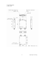
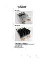
+
PLL Synthesizer
User’s Manual
DPL-4.2GF
DPL-4.2GFH
Digital Signal Technology, Inc.
2-9-10, Kitahara, Asaka, Saitama, 351-0036, Japan
TEL 81-48-470-7030
FAX 81-48-470-7022
URL: http://www.dst.co.jp/
-1-
Digital Signal Technology
Contents
1.
2.
3.
4.
5.
6.
7.
8.
9.
10.
11.
General Description
Specification
Outer Dimensions
Circuit Configuration
Connector, Interface
Thermal Consideration
Control by SPI
Control by Asynchronous Serial data
Shipping Inspection
Warranty
Others
-2-
……………………….
………………………
………………………
………………………
………………………
………………………
………………………
………………………
………………………
………………………
………………………
3
3
5
7
7
8
8
9
10
10
10
Digital Signal Technology
1. General Description
DPL-4.2GF is a frequency synthesizer which can generate any frequency from
50MHz to 4.2GHz,
utilizing PLL technique(Phase Locked Loop) in 1Hz step. It can be used as a clock
source or local oscillator for any application because of its excellent phase noise and
low spurious level. When a sine wave is needed, put a low pass filter at the outside
of the module to remove the harmonics.
2. Specification
Power Supply/Current
Frequency Range
Frequency Resolution
Output Level
Output Impedance
Spurious
Harmonics
Phase Noise 4 GHz(typical)
Internal Reference Clock Accuracy
External Reference Clock and Level
External Clock Input Impedance
Lock Time
Operating Temperature Range
+6V+/-5%、<700mA
50MHz-4.2GHz
1Hz step
>+10dBm
50Ω
< -60dBc
< -8dBc
-80dBc/Hz @100Hz
-97dBc/Hz @1kHz
-102dBc/Hz @10kHz
-105dBc/Hz @100kHz
-126dBc/Hz @1MHz
<±2ppm 0-50 degree C
10MHz -6dBm ~ +6dBm
High Impedance (>1kΩ)
max 5msec
(1) SPI : from SPI_STRB rise
edge to detection of PLL_LD
(2) SCI : from receipt of “CR” to
detection of PLL_LD
0~+50 degree C (In case of
being installed with
Thermal resistance 5.0 degree
C/W heat sink)
Outer Dimensions
50mmx60mmx12.5mm
Weight
about 80gs(module)
about 160gs(including Heat Sink)
(1) Asynchronous Serial
Communication
9600bps、8 bit、1 stop bit、non
parity 3.3V CMOS level
(2) SPI serial communication 3
bytes data 3.3V CMOS level
Interface
-3-
Digital Signal Technology
Phase Noise
-4-
Digital Signal Technology
3. Outer Dimensions
(1)DPL-4.2GF
-5-
Digital Signal Technology
(2)DPL-4.2GFH
-6-
Digital Signal Technology
4. Circuit Configuration
5. Connector, Interface
(1)External 10MHz Input
(2)Output Supply Pin
(3)Power Supply Pin
(4)Internal Freq Adjust
(5)I/F Connector
Pin Assignment
Pin number
1
2
3
SMA-J
SMA-J
50Ω
Feedthrough Capacitor Supply +6V
Frequency adjustment for internal reference clock
2.54mm 5x2 10pin
Connector for Flat Cable
Part number : HIROSE HIF3FC-10PA-2.54DSA
Name
GND
GND
Power Supply
4
INT/EXT
5
LOCK
6
/CS
7
RXD
8
SDI
9
10
TXD
CLK
Description
Signal GND
Signal GND
Power Input +6V
Connected to Feedthrough capacitor
internally
Mode selection pin, External or Internal
reference clock
HIGH: Internal LOW: External
Internally pulled up
PLL lock status output
HIGH: lock
LOW: unlock
3.3V CMOS level
Chip select under SPI mode
Input low active. 3.3V CMOS
Internally pulled up
Asynchronous serial RX data
3.3V CMOS level
Internally pulled up
Serial data input under SPI mode
3.3V CMOS level
Asynchronous serial TX data
3.3V CMOS level
Serial input under SPI mode
3.3V CMOS level
-7-
Digital Signal Technology
6. Thermal Consideration
Power dissipation of this module is about 4.2 watts, so in order to flow heat, mount
this module on chassis firmly. Or, installing heat sink of heat resistance less than
5.0(degree C/W) is recommended. Refer to Page 5 outer dimensions about
mounting holes. It will be more effective if silicon compound is put on the surface of
the mounting section of the module.
7. Control by SPI serial data
(1) SPI specification
Max clock speed
Data bits width
Logic level
20MHz
32bits ( Frequency data bits)
3.3V CMOS
(2) Timing characteristic
Min
Unit
t1
Timing characteristic
Condition
CLK set up time to /CS
50
ns
t2
CLK period
50
ns
t3
SDI set up time to CLK rise edge
10
ns
t4
SDI hold time to CLK rise edge
10
ns
t5
/CS set up time to CLK rise edge
50
ns
Parameter
(3)
Command Definitions
32 bits frequency data is transferred by serial data. Bit definition is as follows.
Bit #
Bit[31:0]
Name
Bit
width
32 bits
Frequency
-8-
Remarks
Frequency data in 1 KHz
resolution in binary
Digital Signal Technology
For example, when you set 4.2GHz, frequency data of Hz unit must be
converted to binary data. Therefore, 4.2GHz is converted to FA56EA00(hex) in 32
bits binary data.
8. Control by asynchronous serial data
How to set from a PC serial port(RS-232C) is explained below.
8-1. Communication specification
Speed
Data bits
Stop bits
Parity
Flow control
Logic level
9600bps
8 bits
1 bit
none
none
3.3V CMOS
8-2. Interface Option
USB interface, USBIF-01 is available as an option for DPL-4.2GF.
8-3. Command definitions
Character strings marked as double quotation marks “ “ means ASCII code. CR
and LF are control codes which means 0D(hex) and 0A(hex). If any invalid
command is entered, “INVALID DATA” CR LF”*” is returned. All characters used
for input should be uppercase. When a normal command is entered, “*” is
returned. Also the entered data is echoed back.
8-3-1. Frequency setting command
For frequency setting, the input can be made in MHz, KHz and Hz unit.
(1) Setting in GHz
For setting 4GHz, input the following data..
“4G”CR
All the data below 100MHz is set to “0”.
In case of setting 4.2GHz, set in MHz like below because a decimal point
cannot be used.
(2) Setting in MHz
For setting 2400MHz, input the following data.
“2400M”CR
All the data below 100KHz is set to “0”.
(3) Setting in KHz
For setting 2400002KHz, input the following data.
“2400002K”CR
Or “2400002”CR
-9-
Digital Signal Technology
8-3-2. READ Command
By entering “READ”CR, the currently set frequency is output. The response is
as follows
“ffffffffKHz”CR LF
“fffffff” shows the frequency of currently outputting in KHz unit.
8-3-3. SAVE Command
By entering “SAVE”CR, the current frequency can be memorized into
EEPROM.
When the power is on next time, the stored data can be output. If any invalid
command is entered, “ERROR”CR LF”*” is returned.
9. Shipping Inspection
100% inspection shall be performed for the electrical specification in 2.
10. Warranty
If any defect is found due to the manufacturer’s improper production or
design within one year after delivery, a repair or a replacement shall be
performed under the manufacturer’s responsibility.
11. Others
11-1. This product, which employs a CMOS device may be easily damaged by
static electricity. Digital Signal Technology, Inc. assumed no liability for
damages that may occur as the result of handling by users even though the
above warranty period.
11-2. Do not supply over voltage power supply, as the module may be damaged.
Digital Signal Technology assumes no liability for the damages that may
occur as a result of handling by users even though within the warranty
period.
Descriptions of this manual are subject to change without notice.
No portion of this manual can be reproduced without the permission of Digital Signal
Technology.
Digital Signal Technology assumed no liability for damages that may occur as a result of
handling by users.
The contents of this manual do not apply to the warranty in executing an industrial property
or other rights, nor permission for the right of execution.
Digital Signal Technology assumes no responsibility for the third party’s industrial property
occurred from using the circuits described in this manual.
- 10 -
Digital Signal Technology