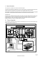
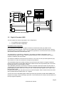
1
ATX 7002 User manual Revision 2.10 May 2008 APPLICOS bv, Veldkampseweg 1, 8181LN, Heerde, The Netherlands 1 1 TABLE OF CONTENTS General information ................................................................................................ 2 1.1 1.2 1.3 1.4 2 Module descriptions ............................................................................................... 5 2.1 2.2 2.3 2.4 2.5 2.6 2.7 2.8 2.9 3 Theory of operation................................................................................................................... 2 Implemented test methods ....................................................................................................... 3 ATX Menu ................................................................................................................................. 4 Program mode .......................................................................................................................... 4 DSP module .............................................................................................................................. 5 Digital I/O module (DIO) ........................................................................................................... 6 High Speed digital I/O module (HSDIO or MFDIO) ................................................................ 10 Signal DAC module (AWG18) ................................................................................................ 11 High speed signal DAC module (AWG16-100) ...................................................................... 11 ADC module (WFD18) ............................................................................................................ 12 High speed ADC module (WFD1470) .................................................................................... 13 Dual reference DAC module (DRS) ........................................................................................ 13 Dual power DAC module (DPS) ............................................................................................. 14 Measurement set-up ............................................................................................. 15 3.1 Programming a measurement Setup...................................................................................... 15 3.1.1 Defining a Stimulus signal ............................................................................................... 15 3.1.2 Using the pattern bits ...................................................................................................... 20 4 Command reference ............................................................................................. 23 4.1 4.2 4.3 4.4 5 6 Overview ................................................................................................................................. 23 Measurement types and related commands .......................................................................... 25 Reset values ........................................................................................................................... 25 General Syntax ....................................................................................................................... 26 Command descriptions ........................................................................................ 27 Specifications........................................................................................................ 54 6.1 6.2 6.3 6.4 6.5 6.6 6.7 DIO module, inputs, outputs ................................................................................................... 54 Specifications AWG18 module ............................................................................................... 55 Specifications AWG16-100 module ........................................................................................ 55 Specifications WFD18 module ............................................................................................... 55 Specifications WFD1470 module ........................................................................................... 56 Specifications Dual reference DAC module ........................................................................... 56 Specifications Dual power DAC module ................................................................................. 56 LIABILITY DISCLAIMER The product described in this manual is warranted in accordance with the terms as set forward in applicable quotations or purchase orders. Product performance is affected by configuration, application, software control, and other factors. The suitability of this product for a specific application must be determined by the customer and is not warranted by APPLICOS. APPLICOS shall not be liable for any special, incidental or consequential damage. Information in this manual is intended to be accurate and reliable. However APPLICOS assumes no responsibility for any errors, which may appear in this document nor does it make any commitment to update the information contained herein. Page 1 ATX7002 user manual 2 General information The ATX7002 is a modular AD- and D/A converter test system. A powerful 32 bit floating point DSP takes care of the signal synthesis. Combined with large stimuli and capture memories, this provides a very powerful tool for analyzing high-speed converters. Via an RS232, the ATX7002 communicates with a PC. Software on the PC gives an easy to use graphic user interface. The IEEE-488 port allows integration of the ATX7002 with other instruments. CAPABILITIES Equipped with the standard ATX7002 modules, the system can measure A/D and D/A converters of up to 16 bit. Higher bit counts can be tested with the special high-resolution modules. The test speed is programmable up to 1MHz. It provides Input signal, Power, and Clocks to the device under test. Pipelined operation of the DUT is handled without any problem. 2.1 Theory of operation The ATX7002 is controlled by a PC by means of commands sent via one of the communication ports (RS232, USB, GPIB, see figure 1.1). ATX7002 POWER SUPPLY ATX7002 system bus DUAL POWER DAC DAC MODULE ADC MODULE* Stimulus generator ROM DSP RAM optical isolation capture logic control logic SpanDAC pattern generator stim.&capt. memory dual DC dac dual DC dac 18bit DAC GAIN CAL 18bit ADC offset DAC offset DAC serial IO power amp DATA communication EXT clock+reset EXT clock+reset CAL MODULE DUAL REF DAC DIGITAL I/O DSP controller module diff single DUT DUT reference power A/ D patternbits + handshaking PC DUT Figure 2-1 ATX7002 block diagram Figuur 2-1 ATX7002 block diagram Page 2 ATX7002 user manual The PC is in control during initialization and during readout of test results. The ATX7002 is in control during the measurement. During initialization of the test, the PC sends some measurement initialization commands to the ATX7002. After this, the ATX7002 takes over control over the measurement as soon as the command "start converter test" comes from the PC. During an A/D converter test, the ATX7002 applies voltages to the device under test, according the contents of the stimulus memory or data processed by the DSP. The converted data is then captured by the digital IO module and stored in memory.. During a D/A converter test, digital data from the digital IO module is applied to the device under test and the analog output voltage is measured and stored in the ATX7002 ADC module.. A 16-bit user-programmable pattern generator, located in the digital IO module, generates 8 universal signals that are available for synchronization between ATX7002 and the device under test. The other 8 signals are meant for internal synchronization. . 2.2 Implemented test methods The following test methods are implemented in the ATX7002. Analog to digital test algorithms A/D ramp test The A/D ramp test applies a user-defined ramp to the converter under test. The ramp steps should be of a higher resolution than the converter under test. The resolution of the ramp steps is dependent on the chosen ATX DAC output span, and the number of steps used. To trigger the ATX DAC module, an external clock or an ATX7002 handshake or pattern bit can be used. The DUT converts each ramp step. Each digital result is stored in the capture memory. The data is captured by means of handshaking or on a user defined time. After the measurement, the contents of the capture memory can be used for offset, gain, INLE, DNLE and TUE calculations. A/D dynamical test A user defined dynamic signal (one or more sine waves) is stored in the stimulus generator, situated in the ATX7002 output DAC. During the measurement, the ATX DAC module applies this stimulus signal to the test board. Every sample (stimuli step) applied by the D/A converter is converted by the DUT. The digital result on the output of the DUT is stored in the capture memory. A/D statistical test A ramp, as used in the A/D ramp test, is applied to the converter several times. The user defines the number of times (sweeps) this ramp is applied. The converter results are stored in DIO capture memory and statistical parameters are calculated from the multiple ramp-codes. The statistical parameter consists of the number of occurrences of each code in the measurement array. Digital to Analog Test algorithms The following D/A converter test methods are implemented in the ATX7002. D/A ramp test Before the measurement, the user defines the start- and end-code and the total number of samples (steps) of the ramp. The ramp can then be calculated and stored in the ATX7002 DIO stimulus memory. During the measurement, the content of the stimulus memory is put via the ATX digital output to the DUT. The DUT converts the digital data to an analog ramp. During the measurement loops, the ATX ADC captures the analog ramp. To trigger the ATX ADC module an external clock or an ATX7002 handshake or pattern bit can be used. Somewhere within the sample-cycle, a programmable clock is used. With the results in the Page 3 ATX7002 user manual capture memory, linearity calculations can be done to get the gain- and offset error and INLE, DNLE, TUE. With several ramps in one measurement it is possible to perform statistical parameter calculations. Note that the ADC performance is best at a 50% clock duty cycle. D/A dynamical test A user defined dynamic digital signal (one or more sine waves) is stored in the DIO stimulus memory. During the measurement, the ATX DIO applies this stimulus signal to the Device under test. The analog result on the output of the DUT is captured by the ATX ADC module. 2.3 ATX Menu The ATX has a scroll and enter button to control the menu. With the scroll button, you can scroll through the available menu options. Pressing the enter button will confirm the selected menu item. The menu has the following structure: 2.4 Program mode For a firmware update the ATX has a special program mode. In program mode the ATX doesn’t accept any module and test commands. The program mode can be entered by holding the enterbutton (of the controller front panel) pressed during a power-up or a reset. Reset the ATX (don’t press the enter-button) to return to normal mode. Page 4 ATX7002 user manual 3 Module descriptions In this section, the ATX7002 modules are described in detail. DSP-CONTROLLER MODULE Signal DAC module Dual power DAC Dual reference DAC ADC module Digital I/O Enter button power supply Scroll button indicators powerdac powerdac DAC output DAC output outputs outputs DAC control DAC control Figure 3-1 ATX7002 frontview The ATX7002 is a modular system. The figure below represents a possible ATX7002, configuration. The communication connectors are situated on the DSP-controller front panel, together with a display, two buttons and 4 LED’s, indicating the four ATX7002 power supply voltages. The display gives the user information about the status of the device and shows a menu to perform some system self tests and change some system settings, without the need of a PC. The two buttons below the display control the display menu and when pressed simultaneously for a few seconds (min. 3 sec.), function as system-reset switch. 3.1 DSP module The DSP controller module controls the ATX7002. All commands received by the DSP via it’s RS232, IEEE or USB port are interpreted and processed by this module. The control of the measurement and all calculations needed before and after a measurement are performed by the DSP module. To prevent ground loops, the communication ports are optically isolated from the ATX7002 system. The DSP controller module is constructed as sketched in figure 2-2. The heart of the module is formed by the DSP-block, in which a Digital Signal Processor is situated for system control and fast post and pre measurement calculations. The DSP also has an address decoder, for selecting and controlling the other DSP module blocks and ATX7002 modules. The communication interface is optically isolated from the system to prevent ground loops with other equipment (like PC or tester). The DSP processor has three types of memory: Flash memory in which the embedded software is programmed, a 512k x32 bit RAM for storing intermediate variable and array- storage, during calculations and communication. In a serial EEPROM, some system settings, like communication settings, are stored. From the back plane, on the most right of the figure, there are coming 4 analog signal lines. These lines are connected to a 4 channel 12 bit A/D converter, and are used for system self test purposes. Two other lines HSI and HSO, are handshake lines and are used for processor controlled handshaking. In this handshaking mode, the DSP controls the measurement -flow and -timing. An address and data bus buffer is situated between the DSP and ATX7002 back plane, to prevent digital activity during pattern generator controlled measurements. Page 5 ATX7002 user manual 32 bit Memory Block COMMUNICATION INTERFACE FLASH RAM 128K 512K Serial EEPROM RS232 USB OPTO-ISOLATION Display DSP ADDRESS & DATA BUS BUFFER IEEE-488 HSI HSO A/D converter A switch interface D AN0 AN1 AN2 AN2 Figure 3-1 DSP module block diagram 3.2 Digital I/O module (DIO) The DIO module can best be described in two configurations: 1. In handshake mode configuration; 2. In pattern-bit mode configuration. Handshake mode configuration In the Handshake configuration, the DSP controls the measurement timing by means of the handshake lines HSO and HSI. In this mode, the update rate is limited by the DSP speed, because the whole timing is controlled by code. The pattern-bit generator is not used in this mode, and serial data transfer is limited to serial data input only. The data stream is controlled by a data MUX. The setting of this MUX is dependent on the measurement type (input or output, serial or parallel operation), and is controlled by DIO controlregisters, initiated by the DSP module. The data I/O is divided over two transceiver sections: one section of 8 bit (the least significant byte) and a section of 12 bit. The sections are for byte-wise operations. The HandShake Output line (HSO) is directly connected to the DIO output via a signal conditioner, buffering and possibly inverting HSO. BHSO (the HSO line before the output buffer) also increments the stimulus memory, when the DIO is output. The handshake input lines come from the connector. The DSP counts the number of HSI events, to calculate when the measurement is ready. The block diagram shows the function of the HSI lines. In parallel data input mode, HSI2 has no function. HSI 1 clocks both input registers. HSI 1 signs to the DSP that data is valid. In serial input mode, HSI1 and HSI2 control the 24-bit shift register. HSI2 controls the shift clock and HSI1 parallel loads the shifted result in to a register. A mux just in front of the MSB register makes byte-wise input operation possible. Both MSByte and LSByte can be input via the lowest byte input lines. The two HSI lines are used to store the bytes in to the input register separately. Page 6 ATX7002 user manual Configured as a data output, data is lead from the DSP or the stimulus memory to the DIO front connector. The two transceivers are both output enabled and set to output (byte-wise output operations are not possible in handshake mode). ATX DIO MODULE IN HANDSHAKE MODE (IM0,1,2,3,20,21) ATX7002 Backplane DATABUS BUFFER ADDRESS BUS BUFFER BHSO BHSI DIO control & registers c c c c c c c c c 24bit register IN C BHSO SHIFT CLK C endaddress DATA MUX PAR.CLOCK HSI 2 hold address counter HSI 1 OUT DIO stimulus and capturememory Left/Right C 24 bit shift register D0 16bit register C 8bit register HSI 1 MUX Static bits register & HSI 2 & MUX C ACTIVE LEVEL IN C C Pol OUT OE CLK C OE C C OE DIR D8..D19 OUT OE DIR D0..D7 DIO FRONT CONNECTOR Figure 3-2 Block diagram of DIO module in handshake mode Two additional registers can be found on the most right of the diagram. These registers are implemented to output static data. The output bits are not changed or read during the measurement and can only be changed or read by means of a command (SDO). The static bits are meant for initial settings on the load board (i.e. relays etc), or for reading out a status from the load board. The bits 2 may also be used for SPI or I C emulation. Page 7 ATX7002 user manual C Patternbit mode configuration In Patternbit mode, the complete measurement flow and timing is controlled by a user programmable pattern bit generator. The DIO block diagram is now more complex, as shown if figure 2-3. ATX DIO MODULE IN PATTERNBIT MODE (IM 10,11,30,31) Capt. mode ATX7002 Backplane DATABUS BUFFER ADDRESS BUS BUFFER BHSO BHSI DIO control & registers c c c c c c Settle loop counter Measure loop counter =1 CLOCK SELECT 1 n Step counter c =0 c =0 c IN OUT hold&reset hold DATA MUX Return OUTPUT BUFFER OE DIO stimulus and capturememory MBHSI BHSO SER_CLK OR & 8 user Pattern bits C C endaddress address counter returnaddress address counter DIO patternbit generator C C OUT C PAR.CLOCK SHIFTCLK Parallel load Left/Right Direction (in/out) D0 16bit register 8 bit register OE CLK 24 bit shift register HB_OE_CLK C OE C & Static bits register LB_OE_CLK MUX & IN HB_OE_CLK BHSO & LB_OE_CLK & OUT OE DIR D8..D19 OUT OE DIR D0..D7 HSI2 OUT DIO FRONT CONNECTOR Figure 3-3 block diagram of DIO in Patternbit mode The handshake lines as described earlier, now have a different function. HSO is now generated by the pattern bit generator, and clocks the stimulus memory in either the DAC module or the DIO. HSO is output to the user, to indicate that an output data or output voltage is going to be changed. HSI1 is not connected and HSI2 is a clock input and is fed directly to a clock source selector. This selector selects the clock source that is applied to the pattern bit generator. The internal clock generators have a frequency of 40MHz (default) and an optional frequency. These can be divided to up to 4096. Hence, the Pattern generator steps through the pattern memory at a programmable step time: Steptime Clockperiod Dividervalue Dividervalue f clock Page 8 ATX7002 user manual C The pattern bit generator has 8 bits that are brought directly to the DIO connector. The highest eight bits of the pattern bit generator control the measurement flow. The other eight bits control the measurement flow: Bit0..B7 Bit8 Bit9 Bit10 Bit11 Bit12 Bit13 Bit14 Bit15 User pattern bits, directly available on the DIO connector To- return address flag, signing the end of the pattern SER_CLK: Serial shift register clock for serial mode IO (positive edge) BHSI store and increment of the capture memory on DIO or ADC (positive edge) BHSO increments the stimulus memory counter on signal DAC or DIO (positive edge) Reserved (not used) User pattern bits-output enable, enables the output of the patternbit (low = enabled) HB_OE_CLK in output mode: enable the highest bits of the output, in input mode it clocks the upper bytes of the data input register, on a positive edge. LB_OE_CLK in output mode: enable the lowest byte of the output, in input mode it clocks the LSB data input register. The start-address of the pattern is programmable. This is to make it possible to store several patterns in the pattern generator. The pattern length is defined by the position of a logic high state of bit 8. The pattern length (number of pattern steps) determines the measurement update rate: The stimulus measurement data (in the DAC or in the DIO module) is updated by HSO, once in the pattern. Hence the Sample time of the measurement is. Sampletime Patternsteps patterntime Patternsteps Dividervalue f clock HSO also increments an on board step counter. The step counter counts the number of steps (or samples) already taken. Depending on the number of stimulus steps to be taken (the stimulus signal length), this counter updates two loop counters. Every time the stimulus memory is looped, one of the loop counters decrements. The user can define the number of times a stimulus signal is applied before the capturing starts, these loops are called “Settle loops”. Once these settle loops are taken the Settle loop counter has counted down to zero the Capture mode line of the back plane will be active and the capturing starts. On each HSI pulse, programmed in the pattern bits, a measurement result is captured by capture memory (on the DIO in case of A/D measurement and on ADC in case of D/A measurement). The contents of the stimulus memory are applied one or more times, depending of the Measurement loops setting. When the measurement loop counter has counted down to zero, the Capture mode line will go to inactive state (negative edge) and the measurement is ready. In the Pattern bit mode, serial input and output is possible. The measurement type determines if the DIO is in input- or in output-mode. The I/O mode determines the direction of the shift register. The shift register is controlled by the programming the pattern bits. Page 9 ATX7002 user manual 3.3 High Speed digital I/O module (HSDIO or MFDIO) The High speed DIO does have 3 operation modes: 1. “Normal” mode 2. High speed output mode 3. High speed input mode In normal” mode the module is fully compatible with the DIO module of the previous paragraph. In high speed output mode the module can generate patterns up to 2 Msamples of 16 bits wide. In high speed input mode the module can capture patterns up to 2 Msamples of 16 bits wide. In high speed mode (input and output) there are 8 static data output lines and 4 static data input lines available. Figure 3-4 block diagram of HSDIO/MFDIO in High Speed Mode Page 10 ATX7002 user manual 3.4 Signal DAC module (AWG18) The Signal DAC module can be seen as a stand-alone waveform generator (AWG: Arbitrary Waveform Generator). The onboard stimulus generator contains an address counter and a 24bit x 512k RAM memory. This memory can be accessed by the DSP. During the measurement, BHSO, the DSP module or an external clock triggers the memory counter. After the measurement the counter can be reset by the DSP module or by an external user reset. The user reset is, as the user clock connected to a LEMO connector. When user reset is kept high, the stimulus generator holds. When user reset is released, then the stimulus memory starts running from its start address (always address 0). A high speed high resolution DAC then converts (also on HSO) the digital stimuli code to an analog signal. If needed, this signal can then be lead through one of the on board 4-th order Butterworth Low pass filters. Two extra DAC blocks are in the module: one DAC module controls the output span of the 18 bit DA converter, the second adds an offset. An output amplifier, with high- and low- sense inputs then buffers the signal. The output can be switched in 4 ways: -1- output disconnected -2- output connected in four wire mode (to compensate for signal loss in cables ) -3- output connected in two wire mode (sense lines are connected internally) -4- output connected in 50 ohms mode (50 ohms output impedance) CAL_GND CAL_FORCE BHSO BHSI ATX7002 SIGNAL MODULE CONTROL WRITE DAC RD/WR MEM c c c c c MODULE ADDRESS & ID LEMO CONNECTOR c HOLD & RESET CLOCK MUX 200kHz LPF DAC stimulus memory +Sense c Data Bus DATA BUFFER 40kHz LPF -Sense c c SPAN ADJUST DAC V SPAN 18 bit DAC DAC ATX7002 BACKPLANE USER CLOCK LEMO CONNECTOR Address& Data Bus c OFFSET ADJUST Figure 3-5 ATX7002 Signal dac module block diagram 3.5 High speed signal DAC module (AWG16-100) The High speed signal DAC module can also be seen as a stand-alone waveform generator (AWG: Arbitrary Waveform Generator) for high speed signals. The onboard stimulus generator contains an address counter and a 16bit x 512k RAM memory. This memory can be accessed by the DSP. During the measurement, BHSO, the Front clock input or 2 internal clock sources can update the memory counter. The module start running when trigger is active or not connected. A high speed high resolution DAC then converts the digital stimuli code to an analog signal. If needed, this signal can then be lead through one of the on board 3-th order Butterworth low pass filters. Two extra DAC blocks are in the module: one DAC module controls the output span of the 18 bit DA converter, the second adds a common mode offset. The output can be switched in 3 ways: -1- output disconnected -2- single ended at positive output (50 Ohm) -3- single ended at negative output (50 Ohm) -4- differential (50 Ohm) Page 11 ATX7002 user manual BP-TRIGGER BP-CLOCK SIGNAL MODULE CONTROL WRITE DAC RD/WR MEM MODULE ADDRESS & ID EXTERNAL TRIGGER EXTERNAL CLOCK (in/out) 100 MHz INTERNAL CLOCK SOURCE CLOCK LOGIC 70 MHz INTERNAL CLOCK SOURCE 30MHz LPF 15MHz LPF DAC stimulus memory Out+ 16 bit DAC ATTENUATOR 6MHz LPF 50 DC-OFFSET DAC (16bit) DAC V-Range DATA BUFFER Data Bus DAC BACKPLANE CONNECTOR Address& Data Bus Out- Single to Differential stage RANGE DAC (16bit) Figure 3-6 ATX7002 High speed signal dac module block diagram 3.6 ADC module (WFD18) The ADC module (WFD: WaveForm Digitizer) has a comparable design as the signal DAC module. It contains a 24bit x 512k capture memory and address counter, which can be read and written by the DIO. During the measurement an external clock or BHSI or the DSP triggers 18 bit AD/converter. A conversion ready signal from the AD converter triggers the capture memory and counter. The user CAL_GND CAL_FORCE c c c c c MODULE ADDRESS & ID READ ADC RD/WR MEM BHSO BHSI HOLD & RESET c CLOCK MUX end of conversion 200kHz LPF +input 40kHz LPF ADC capture memory c Differential to single ended rangable amplifier 18 bit ADC - input OFFSET CAL GAIN CAL DAC c DAC c GAIN c DATA BUFFER ATX7002 BACKPLANE USER CLOCK LEMO CONNECTOR LEMO CONNECTOR Address& Data Bus ATX7002 ADC MODULE CONTROL Data Bus Figure 3-7 ATX7002 ADC module block diagram reset is similar to the reset on the signal DAC module. The input stage is formed by a differential to single-end amplifier, This amplifier can be programmed to three different input ranges. Before conversion the signal can be lead to one of the on board 4-th order Butterworth Low pass filters. It is possible to switch the input to a single ended input configuration. The negative differential input is then internally switched to ground. The input impedance is switchable from high impedance to 50 ohms. Page 12 ATX7002 user manual 3.7 High speed ADC module (WFD1470) The ADC14-70 module is intended for high-speed waveform capturing . It contains a 16bit x 256k capture memory and address counter, which can be read and written by the Controller. Figure 3-8 ATX7002 high speed ADC module block diagram The External Clock and Trigger input allow the user to control the capturing of data. The External Clock is the Sample Clock while the Trigger input allows a user defined start of data capturing. The analog input is a differential input. By switching one input to ground or to the programmable DC Offset source it becomes a single ended input with programmable DC mid level. 3.8 Dual reference DAC module (DRS) The ATX dual reference DAC module (DRS: Dual Reference Source) contains two high precision 20bit DA converters, that operate independently (output switches and levels are programmed for each separate channel). The output stage has an output level range of +/- 6.50 Volts. The output current is limited to +/- 10mA. Between the DAC and the output stage a low pass filter blocks out noise, extending the module settling time to 500us. The output stage can be switched from 4 wire to 2 wire output mode. CAL_GND CAL_FORCE Address& Data Bus ATX7002 REFDAC MODULE CONTROL c c c LEMO CONNECTOR c LEMO CONNECTOR -Sense 20 bit DAC LPF +Sense c 20 bit DAC -Sense ATX7002 BACKPLANE LPF +Sense MODULE ADDRESS & ID c Figure 3-9 Dual reference dac module block diagram Page 13 ATX7002 user manual 3.9 Dual power DAC module (DPS) The Dual power dac module (DPS: Dual Power Source) has the same design as the dual reference module. The output stage is replaced by a power amplifier. The range of the module is set to +/13.5V and the output current is limited to 250 mA. Again, the output stage can be set to a four and a two-wire configuration. Page 14 ATX7002 user manual 4 4.1 Measurement set-up Programming a measurement Setup 4.1.1 Defining a Stimulus signal Before defining a signal in the stimulus, the used stimulus memory size (the number of stimulus steps or samples) (SS) should be defined. The stimulus memory is situated in the ATX7002 signal DAC module and is used as stimulus generator during A/D converter tests, The digital I/O module contains a memory which is used as stimulus memory during D/A measurements. In fact, one stimulus step is the content of one stimulus memory address, each 24 bits wide. The maximum stimulus memory size is 524288 steps. The stimulisteps definition is done with the command: SSn example: SS23 n is a decimal number between 2 and 524288 defines a stimulus memory size of 23 samples. During the measurement, the contents of the stimulus memory can be repeated (looped) several times. In figure 3-1 on the next page, the stimulus memory contains 23 data steps, the loop is drawn as a circular arrow. The number of loops can be configured by the user. Two types of loops can be configured: Settle loops: Loops, before the measurement, to let the signal settle before the measurement, this is especially used for measurement setups with filters. The capture memory is not capturing converted data. The minimum number of settle loops is 0, the max number is 255. The settle loops definition is done with the command: SLn example: SL4 n is a decimal integer between 0 and 255 4 settle loops before the measurement. Measurement loops (ML): loops that directly follow the settle loops, The capture memory stores now every single measurement step. Like the settle loops, the maximum number of measurement loops is 255. The measurement loops definition is done with the command: MLn example: ML10 n is a decimal integer between 1 and 255 The measurement takes 10 measurement loops. When each loop has 23 samples, the capture memory captures 230 values The capture memory can capture 524288 conversion results. During A/D type measurements, the capture memory is positioned in the ATX DIO. During A/D type measurements the capture memory is situated in the ADC module. When the number of results recorded in the capture memory exceeds the memory size, the capture memory address counter stops and capturing of data will be terminated. The size of capture data can be easily calculated by multiplying the number of measurement loops with the number of stimuli steps. (ML*SS) . For MT15 the number of measurement loops can be up to 8191, see paragraph “Digital Ramp stimulus for MT15” for more information. When the first measurement loop starts, the capture memory starts to capture data. Due to pipelining, the device adds a certain latency, which is called the device latency. The user should define this device latency. The device latency definition is done with the command: DLn example: DL2 n is a decimal integer between 0 and 14 The device has a pipelining of 2 cycles. Page 15 ATX7002 user manual Analog Sine stimulus When defining an analog sine stimulus, it is possible to define up to 10 different sine waves within one stimulus signal. The amplitude, phase and the number of periods within the defined stimuli size (the number of periods within one loop) should be defined for each sine wave. In addition, one common offset for all sine waves can be defined. First, the measurement type is chosen with the MT command MT2 Select A/D sine test. The analog sine definition is done with the command: ASn,[volts],[periods],[phase] n is a decimal integer from 0 to 9. With [volts] the amplitude (top) is defined and [periods] defines the number of periods within the defined number stimuli steps and phase defines the starting angle (degrees) of the sine. Example: AS0,0.01,1,0 Define a sine wave, amplitude 10mV, one period starting angle 0 degrees. An offset voltage can be defined as follows: AOvolts the offset voltage [volts] defined here is added to all defined sine waves. Example: AO0 The analog offset is 0 volts. The ATXDAC utilization depends on the command AU (analog utilization) . When set to 1.0 the maximum resolution of the ATXDAC is used. Set to 0.9, 90% of the ATXDAC range is used. Now, the sample-time (or Cycle time) can be defined. In handshake mode it is hard to define a cycle time, because of handshake timing uncertainty. In patternbit mode TC can be calculated using the formula: TC Patternbitsteps Steptime Patternbitsteps Dividervalue f clock Where “Pattern bit steps” equals the number of steps of the pattern programmed in the pattern bit generator; Step time equals the time taken for each pattern bit step. This step time is set by choosing the pattern bit clock source and divider value (refer to the PBC command for more information) The sine frequency can be calculated with this formula: fn periods SS TC Where SS is the number of stimulus steps and TC is the cycle time (in seconds) After defining the measurement type, number of stimuli steps, the analog sine(s), the offset voltage and de ATXDAC utilization, The ATX DSP controller module should calculate the stimuli values and store it to the stimulus memory. This is done with the command: SF Calculate stimulus data and fill the stimulus memory. The calculation is dependent on the defined measurement type. In figure 3-3 the sampled sinewave as defined in the examples above :(stimuli steps 23, 10 mV Sinewave amplitude, 0 volts offset, 1 period, 0 degrees phase) is projected. : Page 16 ATX7002 user manual First loop second loop Cycle time Ampitude 0mV AS0,0.01,1,0 AO=0 1 2 3 4 5 6 7 8 9 10 11 12 13 11 15 16 17 18 19 20 21 22 23 1 2 3 4 5 6 7 8 9 10 11 12 13 11 15 16 17 18 19 20 21 22 23 Figure 4-1 Example of a sampled sinewave Digital Sine stimulus The digital sine stimulus has the same definition protocol as described at the Analog sine stimulus. The measurement type is chosen with the MT command. MT12 Select D/A sine test. Now, the DIO outputs the contents (up to 20 bits) of the DIO stimulus memory. The ATX ADC should be set in a correct range with the command RAn command. The only commands that differs from the analog sine definition are the ones defining the sine wave(s) and offset. The digital sine definition is done with the command: DSn,[hex amplitude],[periods],[phase] n is a decimal integer from 0 to 9. The first sine should always be defined in sine 0, if not, all following sines are neglected. With [hex amplitude] the amplitude is defined, in hexadecimal notation, [periods] defines the number of periods within the defined number stimuli steps and [phase] defines the sine starting angle. example: DS0,100,1,0 Defines a sinewave, amplitude 100hex , one period, phase=0. The offset, on which the sine(s) are added, should always be larger than the maximum amplitude of the defined sines. After reset, the standard digital offset is set to 80000 hex. Hence when the digital offset is 80000H, the maximum sine amplitude is 7FFFF hex, since the DIO I/O bus is 20 bits wide. When another offset is used, the maximum sine amplitude decreases. The digital offset can be defined as follows: DOhex Example: The digital offset of [hex] defined here, is added to all defined sinewaves. DO110 The digital offset is 110 hex. Page 17 ATX7002 user manual Figure 2-5 shows the output op the ATX digital output during the first two measurementloops, when a digital sine is defined as described in the examples above. first loop second loop 200hex 180hex DO=110hex 100hex 080hex 000hex Figure 4-2 Example of a digital sinewave Analog Ramp stimulus An other way of testing an A to D converter is to apply a high-resolution ramp voltage to the converter under test. (A/D ramp test) From the converted data, the converter linearity can be calculated. The measurement type is chosen with the MT command MT1 Select A/D ramp test Applying multiple ramps makes it possible to get statistical and noise figures. The maximum resolution of the ramp applied is equal to the sweep voltage (start voltage AN - end voltage AX) of the ramp divided by 262144 (the number of converter steps). When not using the program ATVIEW, care should be taken defining the number of stimuli steps, to get a proportional ramp. For a Ramp the MAXIMAL number of stimuli steps = 262144. Stimuliste ps( SS ) Number of DUT steps number of samples per DUT step 2 DB samplesteps During the measurement, the ramp is applied several times to the device under test, dependent on the setting of the number of settle loops and measurement loops. Because of the relative high step between the end of the ramp and the start of the next ramp, it may be necessary to wait a few sample-times before the next ramp starts, to let the ATX DAC output voltage and the test setup settle to the new voltage. The numbers of the so-called settle conversions can be set with the commands SC. This command adds a number of steps to the stimulus memory, containing the start voltage of the ramp: Example: SC3 adds three settle conversion at the start of each measurement loop. Page 18 ATX7002 user manual In the figure below, a total of three settle conversions are added to the stimuli steps. Settle conversions Stimuli steps Settle conversions ramp end voltage TC ramp start voltage resolution step One measurement loop Figure 4-3 Ramp with 3 settle conversions included The command “AN“ sets the start voltage of the ramp, “AX” sets the end voltage of the ramp. example: a 10 bit converter is to be measured. The zero scale voltage is 0 volt, the full scale voltage is 3.5 Volts. Each converter step must be sampled with 8 times the DUT resolution AN0 AX3.5 SS Sets the ramp start voltage to 0 Volts. Sets the ramp end voltage to 3.5 Volts. 210 times resulution 1024 8 8192 After defining the measurement type, stimulisteps ramp start and end voltages, the ramp is calculated and stored in the stimulus memory with the “stimuli fill” (SF) command. Digital Ramp stimulus The digital ramp is defined the same way as done with the analog ramp. Now, the digital output buffers output the ramp signal in digital form. The measurement type is chosen with the MT command: MT11 Select D/A ramp test. The number of stimuli steps (SS) is calculated with the formula: SS Startvalue Stopvalue 1 The 16 bit start and stop values of the ramp can be defined with the commands DN and DX: DN0000 Define digital start value to 0000 hex DX0E00 Define digital end value to E00 hex. The number of stimuli steps should be given in decimal, and is in this example 3584 + 1 = 3585 steps: SS3585. Digital Ramp stimulus for MT15 For MT11 each DUT converter step is converted once for each ramp. Each measurement loop (ML) will repeat a complete ramp with a maximum of 255 or till the capture memory is full. With MT15 each converter step can be converted many times. The number of conversions per converter step can be defined with the command ML (measurement loops), with a maximum of 8191. If the results don’t fit into the capture memory, the total test is will be split into cycles. Between the cycles, the results are read from capture memory (ADC memory) and stored into memory of the controller. Each cycle will consist of a complete ramp and the stimulus signal will not be updated between the cycles. The results of each DUT converter step will be averaged. Optionaly the outliers per converter step can be removed, see command OL. Page 19 ATX7002 user manual Example: DB14 (14 bit DUT) SS16384 DN0 DX3FFF SC0 ML64 The maximum number of measurement loops per cycle is: capt. mem./(SS+SC) 512k/16k = 32 So the total test takes 2 equal cycles. Each cycle consists of 1 ramp with 32 conversions per dut converter step. If the number of measurement loops is e.g. 61 (prime number), this test should take 61 cycles! So avoid using prime numbers for the number of measurement loops. After defining the measurement type, The number of stimuli steps, and start and end values, the ramp is calculated and stored in the stimulus memory with the “stimuli fill” (SF) command. 4.1.2 Using the pattern bits In Pattern bit mode, the timing of the measurement is dependent on the pattern bit generator. In this section, an example is given on how to program a pattern in the pattern memory of the generator. Example case: An A/D converter of 10 bits is to be tested. The converter has an update rate of 100kHz. A conversion is started with a sample line, which is high active, the result is output from the device if a read line is low. The device has 10 data lines (Not a byte-wise data flow) The pattern bit clock is set so that one pattern step takes 1 us (to minimize the number of pattern bit steps in this example for optimized timing it is better to use a higher clock rate). The desired timing can now be sketched: Page 20 ATX7002 user manual PATTERN width BHSO bit11 DAC VOLTAGE bit0 USER Patternbit1 bit1 USER Patternbit2 Converter DATA bit14 HB_OE_CLK bit15 LB_OE_CLK bit10 BHSI for capturing data bit8 RETURN FLAG user bits output enable Bit13 1 2 3 4 5 6 7 8 9 10 11 12 13 The programming of the patternbit generator clock is done with the commands PBC. To get a 1 us step time, the internal 40MHz clock is used, and divided by a factor 40: send the command PBC1,40 to program the pattern generator clock source. The pattern bits now can be edited. The pattern bit edit mode is entered by sending the command PBE. The edit mode stops when the ATX7002 receives character E Now we’re in the Edit mode We start programming bit 11, BHSO, in the sketch we see that BHSO is low for the first 12 steps and high for 1 step: -send the command B11 to select bit 11 -send command L12 , for programming the first 12 steps low -send command H1, for programming one step high Next we program bit 0: user pattern bit 1. This bit clocks the device under test 11.In the sketch patternbit1 is first 4 steps high, and 9 steps low: -send the command B0 to select bit 0 -send command H4 , for programming the first 4 steps High -send command L9, for programming the following 9 steps Low Next we program bit 1: user pattern bit 2. This bit is connected to the read pin of the device under test In the sketch patternbit2 is first 9 steps high, then 2 steps low, then 2 steps high: -send the command B1 to select bit 1 -send command H9 , for programming the first 9 steps High Page 21 ATX7002 user manual -send command L2, for programming the following 2 steps Low -send command H2 , for programming the last two steps High Next we program bit 14 (HB_OE CLOCK), this bit clocks the digital result in the DIO input register. In the sketch, this bit is high on the 11-th step: The bit can be programmed in the same way as described above. The commands entered may be separated by semicolons: B14;L10;H1;L2 LB_OE CLOCK (bit 15) has the same timing and can be programmed the same way: B15;L10;H1;L2 BHSI, the bit that clocks the captured data in the capture memory is bit 10. This bit is high during the twelfth step: B15;L11;H1;L1 BHSO, (Bit 11) is the bit that clocks the next stimulus data and updates the ATX DAC. This bit is high during the last step NOTE THAT BHSO MAY NOT BE HIGH AT THE SAME TIME AS BHSI! B11;L12;H1 The return flag, signing the last pattern bit step, is high only during the last step. This bit is bit 8: B8;L12;H1 Finally, bit 10, that enables the user pattern bits should be low the whole pattern sequence. B13;L13 We leave the pattern bit edit mode by sending: E For a more detailed description of the pattern bits please refer to section 2.2 describing the DIO and the pattern bit generator. For more information on programming the pattern bits, please refer to the command description describing the PBE command. Page 22 ATX7002 user manual 5 5.1 Command reference Overview The ATX7002 may be programmed by means of commands that are passed through one of the communication links (RS232, USB or IEEE-488). The following commands are available: General command information Page Measurement types and related commands Reset values General syntax Command description Syntax Page Abort current action ESC-C 24 Set Analog full scale Set Device Analog Gain Set Analog input Offset voltage Set Analog ramp minimum Set Analog Offset for sine waves Set Analog Sine Set Analog Utilization factor Set Analog ramp maximum Set Analog Zero scale AF AG AI AN AO AS AU AX AZ 27 27 27 28 28 28 29 29 29 Card select Set RS232 baud rate Connect Card High speed DIO Clock Calibration Delay values High speed DIO Clock Delay values Calibrate Digital Output levels Set module Gain Calibration Set Module ID in module Set IEEE Address Set module Offset Calibration Module configuration in controller CRC check Select module Clock source Store module calibration values Set module output voltage/read module input voltage C CBAUD CC CCLKD CLKD CDIOV CGAIN CID CIEEE COFFSET CMOD CRC CS CSTORE CV 29 30 32 31 31 27 32 32 33 33 33 34 34 34 34 Set number of Device Bits Disable Error Messages Set Mode of HSDIO/MFDIO Set Digital Output level Set clock Divider Set Device Latency Set Digital ramp Minimum Set Digital sine Offset Set Digital Sine Set device type Set Digital ramp Maximum DB DEM DIOM DIOV DIV DL DN DO DS DT DX 35 35 35 35 35 36 36 36 36 37 37 Set FS-mode FS 37 Set gain and connection mode of S2D+GA Module Set test-board Offset-Gain GA GO 38 38 Set Handshake mode HM 38 Page 23 ATX7002 user manual Identification string Set Io Mode Command description ID IM Syntax 38 39 Page Read and write digital IO port Read/write handshake lines IO IOHS 43 43 Calculated measurement parameters Set Measurement Loops Lock/Unlock Module Set Module Data edit Address Module Memory data Dump Module Memory data Load Module Memory single data Read Set module memory return address Module Memory single data Write Set Measurement Type Execute measurement M ML MLOCK MMA MMD MML MMR MMSMMS MMW MT MX 44 44 45 45 45 45 45 46 46 46 46 Outliers Output measurement results OL OM[B] 47 47 Pattern Bit generator start Address Pattern Bit Clock source and divider Pattern Bit Edit mode Pattern Bit Return Address Production mode PBA PBC PBE PBR PMODE 47 47 48 49 49 Range RA 50 Set attenuation and connection mode of S2D+GA module Set number of Settle Conversions Read Static Input Data Read or write Static Output Data Fill Stimuli Memory Set Settle loops Stimuli Steps Set number of sweeps S2D SC SDI SDO SF SL SS SW 50 50 50 50 51 51 51 52 Set DAC or ADC cycle-time Set timeout time Set trigger mode Set settle time Perform self-test TC TO TRG TS TST 52 52 52 53 53 Wait WAIT 53 Page 24 ATX7002 user manual 5.2 Measurement types and related commands MT1 A/D ramp test SS, ML, SL, TC, TO, DB, DL, DT, AO, AN, AX, AZ, AF, AG, AI, GO, SC,CS,IM,HM MT2 A/D sine (dynamical) test SS, ML, SL, TC, DB, DL, DT, AO, AS, AZ, AF, AG, AI, GO,AU,CS,IM,HM MT3 A/D user defined pattern measurement MT4 A/D Statistical and Noise Test SW, SS, TC, TO, DB, DL, DT, AO, AN, AX, AZ, AF, AG, AI, GO, SC,CS,IM,HM MT11 D/A ramp (linearity) test SS, ML, SL, TC, TO, RA, DB, AZ, DN, DX, AF, DL, ST, SC,IM,HM MT12 D/A sine (dynamic) test SS, ML, SL, TC, RA, DB, DS, DO, AZ, AF, DL, ST,IM,HM MT13 D/A user defined pattern measurement Overall measurement settings: Fill/update stimulus memory: Pattern bits: Reference/Power voltages: 5.3 SF PBC, PBA, PBR CV Reset values The following table gives the default values for commands after reset. AF AN AO AX AG ASn AZ C CBAUD CC CS CV 5 Volt 0 Volt 0 Volt 5 Volt 1 0,0,0 0 Volt dac module 57600 eeprom 0,0 0 0Volt,0Volt DB DL DN D0 DX DS DT DEM ML 8 0 0 0x0 0 0,0,0 0 0 1 MT PBA PBR PBC RA SC SL SS TO TS 1 0 0 1,1 4 0 0 0 1000 250 eeprom = value restored from eeprom, when written value is stored in eeprom. Page 25 ATX7002 user manual 5.4 General Syntax Commands are specified by the following general syntax. KEYWORDn<term> where: KEYWORD param <term> is a command string is a parameter (optional) or a question mark is a terminator The command string exists of multiple 7-bit ASCII characters. The command parameters (param) may be one of the following types: volts dec Free ASCII format voltage specification [-]n.nnnnnn Examples: -1.5 3.123456 Free ASCII format decimal value specification [-]n.nnnnnn hex A string of hexadecimal ASCII digits (0..9, A..F). The first hexadecimal digit is the most significant digit. n A number containing a single or multiple numeric ASCII digits. These digits form a number. The terminator is a CR, LF, : or ; . The ATX sends a CR, after each string. Multiple commands may be chained with the ; or : character. Example: AN0;AX3;SS4096; When parameter n is a question mark, the current value for n is returned. Example: AX1.2 Set Full Scale value to 1.2 Volt. AX? Returns "1.200000" Page 26 ATX7002 user manual 6 Command descriptions The available commands are described in this section. There is one special command that follow a different syntax: <ESC>C This command may be issued at any time and returns the ATX7002 to the command mode. The settings are not changed. Set Device Analog Full scale AFvolts AF? AF Set the device full-scale value Return current full-scale value. The Device under test (ADC or DAC) Full Scale value specifies the voltage level corresponding to the expected full scale level (often equal to Vref). The parameter is used to calculate the expected output value (analog or digital) of the DUT, after a conversion, for the error calculations. Example: AF1.20 AF? Set Full Scale value to 1.20 Volt. Returns "1.200000" Related commands: AZ, AG, AO, AI, GO Set device Analog Gain AG AGdec AG? Set the analog gain of the test-setup. Return current value for the analog gain. After the DUT parameter definition, like full-scale voltage (AF), zero scale voltage (AZ) number of device bits (DB), it is possible to calculate the ideal conversion result because for each conversion result, the corresponding ATX DAC output voltage is known. However, when on the test board, an input amplifier or a filter is situated, the expected code on the output is unknown due to signal gain or attenuation. With the Analog Gain command, the user can define the attenuation or gain of the signal-path between the ATX DAC output and the device input. Example: AG0.95 Sets the Analog gain to 0.95. When testing an A/D converter this means that when the ATX DAC outputs 1 Volt, the converter has a 0.95 input voltage. AG? Returns “0.950000” Related commands: AO, AG,AI, GO Set Device Analog Input offset voltage AIvolts AI? AI Set the analog input offset voltage. Return current value for the analog input offset voltage. This command defines the actual device input offset voltage or ATX ADC input offset. This parameter is only used if parameter GO is set to 0. For A/D measurements, it is possible that a DC component programmed in the voltage from the ATX DAC is blocked out of the DUT input signal, due to filtering. In this case, it is possible that an offset voltage is applied to the device input by an external reference source or by the input amplifier stage. This voltage should be known to calculate the expected output codes of the DUT. Example: AI1.25 Sets the device input offset voltage to 1.25 Volts. The AC component of the DAC voltage is added to this value, to calculate the expected output code. AI? Returns 1.25 Related commands: GO Page 27 ATX7002 user manual Set Analog ramp minimum ANvolt AN Set the Analog minimum voltage, which is used for calculating the analog ramp. Returns the current value of the Analog minimum AN? When using the Ramp measurement, AN configures the starting voltage of the A/D ramp .The negative reference voltage of ATX output DAC is programmed to this voltage, meaning that the lower limit of the ATX DAC voltage is set by this command. example: AN0 AN? Sets the ramp start voltage to 0 Volts. Returns “0.000000”. Related commands: AX Set Analog Offset for sine waves AOvolts ,[m] AO? AO Sets the analog offset and optional connect the offset (m) Return current value for the analog offset (and connetion status). The offset voltage [volts] defined with this command, is added to all defined sine waves. The offset is not used during ramp-measurements. Some modules (e.g. DAC16-100 or WFD1470) do have a (common mode) offset input or output voltage. This command will program this DC voltage and connect (1) or disconnect this voltage with the optional parameter m. Example: AO1.5 Set the analog offset to 1.5 volts. AO? Returns “1.500000” Related commands: AS Set Analog Sine AS ASn,volts,periods,phase ASn? Define the amplitude (top) in volts, number of periods and phase in degrees within the defined stimulus size, of sine n (n=0..9). Return the current amplitude, number periods and phase of sine n This command defines the stimulus signal parameters for harmonic A/D converter tests. It is possible to define up to 10 different sine waves. Definition should start with sine 0. All sine waves are added and stored in the stimulus memory. The sine waves can be defined by giving the amplitude (top), and the number of periods within the defined stimuli size (SS). An offset (used for all sines) can be defined with the AO command. De frequency of the sine wave is depending on the number of periods defined here, the number of stimuli steps and the stimulus clock period time. This sample clock can be either fn periods SS t (clock ) an external (user) clock or a clock generated by the pattern bits (BHSO) or BHSI, see the CS command for details. The number of periods should be an integer higher or equal to one, the phase is a float variable, defining the sine wave phase in degrees. NOTE: After defining the sine waves, the stimulus memory size, the stimulus memory should be updated with the “Stimuli Fill” command (SF) . The ATX DAC ranging is automatically set to the minimum and maximum signal level, in the stimulus signal. Page 28 ATX7002 user manual example: AS0,1.235,3,10.5 AS0? Define sine 0 with an amplitude of 1.235 volts, three periods and a phase of 10.5 degrees. Returns the parameters of sine 0. “1.235000,3,10.5” Related commands: AO, SS, SF, CS Set Analog Utilization factor AU<value> AU? Example: AU0.90 AU? AU Set the ATXDAC utilization factor Return the current utilization factor Set ATXDAC utilisation to 90 % Returns "0.900000" Only for MT2 (ADC dynamical test). Set Analog ramp maXimum AX AX<value> - sets the value of the Analog maximum (Volts) this value determines the output sweep of the ATX DAC - Returns the current value of the Analog Ramp maximum AX? When using the Ramp measurement, AX configures the end voltage of the A/D ramp. In combination with the AN parameter, AX determines the output sweep and ATX DAC resolution. The atx DAC sweep can be easily calculated by subtracting AN from AX. The resolution of the 18 bit ATX DAC can calculate: resolutionstep outputsweep 262144 AX AN (V ) 262144 Example: AX2.25 AX? Sets the ramp start voltage to 2.25 Volts. returns “2.250000”. Related commands: AN Set Device Analog Zero scale AZ AZvolts AZ? Set the Device Zero Scale value Return the current Device zero scale value AZ specifies the voltage level corresponding to the zero scale level of the ADC or DAC under test (often equal to GND). The parameter is used for the calculation of the expected output value (analog or digital) of the DUT, after a conversion, for the error calculations. Example: AZ0.10 AZ? Set Full Scale value to 1.20 Volt. Returns "0.100000" Related commands: AF,AG,AO,AI,GO Select Card Cn C? C Set Card (module) n the currently selected card (n=0..9). Returns currently selected card. This command selects one of the Cards (modules). All other Card Setting commands operate on the selected Card only. It is also possible to select the card by typing the card number in front of these card setting commands. This makes the use of the C command needless. Page 29 ATX7002 user manual Example: C2 C? 2CC1 Select Card number 2 for further operations. Returns "2". Select Card 2 and execute the CC1 command (card connect) Set Baud rate CBAUD CBAUDn CBAUD? sets the RS232 Baudrate to value n. returns the current Baudrate setting The Baud rate of the serial communication may be changed to one of the following values: 9600 19200 38400 57600* Example: CBAUD19200 CBAUD? * Factory setting Set the Baud rate to 19200 Baud. Returns "19200". Card Connect CCn,m CC? CC Set connection of the currently selected Card Return current Card connect setting. The currently selected module may be switched by this command. In case of a signal DAC (AWG18) module, n selects the way the output signal is connected to the connector: In four wire mode (+Force +Sense, GND and GND sense), in two wire mode (The sense lines are internally connected to +force and GND) and in two wire 50 ohms mode. (The output impedance of the module is 50 ohms). m selects the internal low pass filter setting : signal DAC (AWG18) n 0 Disconnected module 1 connect in 4 wire mode 2 connect 2 wire mode 3 connect 2 wire, 50 ohms m 0 1 2 Bypass all filters Lead signal through LP filter 1 (40kHz) Lead signal through LP filter 1 (200kHz) High Speed signal DAC (AWG16-100) n m 0 Disconnected module 0 Bypass all filters 1 connect positive output* 1 Lead signal through LP filter 1 (6MHz) 2 connect negative output* 2 Lead signal through LP filter 1 (15MHz) 3 connect differential* 3 Lead signal through LP filter 1 (30MHz) *Always 50 Ohm connected In case of an ADC module, n selects the input mode (Differential or single ended) and input impedance (50 ohms or 10 M ohms) of the ADC module. ADC module (WFD18) n 0 Disconnected module 1 connect ,differential input mode 10M ohm 2 connect, differential input mode 50 ohm m 0 1 2 Bypass all filters Lead signal through LP filter 1 (40kHz) Lead signal through LP filter 1 (200kHz) In case of the high speed ADC module the n parameter is split in 2 digits n1 and n2. n1 (upper digit) for the positive input, n2 (lower digit) for the negative input. Page 30 ATX7002 user manual ADC14 module (WFD1470) n1/n2 0 Disconnected input 1 connected, 10kohm 2 connected, 50 ohm AC 3 connected, 50 ohm DC 4 connect to gnd, input disconnected 5 connect to gnd, input connected m 0 1 2 Bypass all filters Lead signal through LP filter 1 (6MHz) Lead signal through LP filter 2 (15MHz) Lead signal through LP filter 3 (30MHz) examples: 14: connect positive input 10k and negative input to gnd and input relay of negative input open. 22: connect positive and negative input 50 ohm AC 05: positive input relay open, connect negative input to gnd and connect input relay If the card has two channels (in case of a reference DAC or power-DAC ) m determines the way the second channel is switched Reference dac and powerdac: n 0 Disconnected channel 1 1 connect channel 1, 4 wire 2 connect channel 1, 2 wire Example: CC1, 2 CC? CC0,0 m 0 1 2 Disconnected channel 2 connect channel 2, 4 wire connect channel 2, 2 wire Signal DAC: Connect in 4-wire mode using internal 200kHz LPF. Reference: connect channel 1 in 4 wire mode and channel 2 in 2 wire mode Returns "1,2". Disconnects the card. Set High Speed DIO Clock Calibration data CCLKDn,m,o CCLKD? CCLKD set the calibration values in ns returns the current calibration settings These values are factory settings. Do not changes these values. Set High Speed DIO Clock delay(s) CLKDn,m CLKDn? CLKD set the delay of clock n in ns returns the current delay of clock n High speed input mode: t1 for n=0 t2 for n=1 Page 31 ATX7002 user manual High speed output mode: t1 for n=0 t2 for n=1 Calibrate Digital Output levels CDIOVcode,[minv],[maxv] CDIOV? CDIOV Calibrate level of digital output lines (DIO) Return the current calibration settings of digital output lines. The last two parameters, minv and maxv, are optional. Code is a value between 00 and FF hexadecimal. With code 00 the digital output level is programmed to minimal voltage, with code FF to maximal voltage. If both voltages are measured, send this command with both voltage filled in to the ATX7002 (code may be any value). Calibrate Gain CGAIN CGAINn[,m] CGAIN? Set gain value(s) Return gain value(s) Write gain value to selected module. Signal DAC: n is gain value of the offset dac. Gain should be calibrated at –5V and +5V. m is gain value of the range dac. Gain should be calibrated at 0 and 10 V. Signal ADC: n is gain value of ADC. Gain should be calibrated for each range. Power DAC: n is gain value of channel 1. Gain should be calibrated at –10V and +10V. m is gain value of channel 2. Gain should also be calibrated at –10V and +10V. Reference DAC: n is gain value of channel 1. Gain should be calibrated at –5V and +5V. m is gain value of channel 2. Gain should also be calibrated at –5V and +5V. Store values in the module eeprom after calibration with the command CSTORE. Related commands: COFFSET, CSTORE Set module identification CID? CID Returns the module identification of the currently selected module Page 32 ATX7002 user manual With CID, the module identification of the currently selected module can be read. This value should correspond with the CMOD command. See CMOD command for more information about module codes. Set IEEE address CIEEEn CIEEE? CIEEE Set IEEE address Return IEEE address IEEE address should be in a range from 0 to 30. Calibrate Offset COFFSET COFFSETn,[m] Set offset value(s) (Hex.) COFFSET? Return offset value(s) Write offset value to selected module. Signal DAC: n is offset value of the offset dac. Offset should be calibrated at 0V. m is offset value of the range dac. Offset should be calibrated at 5 V. Signal ADC: n is offset value of ADC. Offset should be calibrated for each range. Power DAC: n is offset value of channel 1. Offset should be calibrated at 0V. m is offset value of channel 2. Offset should also be calibrated at 0V. Reference DAC: n is offset value of channel 1. Offset should be calibrated at 0V. m is offset value of channel 2. Offset should also be calibrated at 9V. Store values in the module eeprom after calibration with the command CSTORE. Related commands: CGAIN, CSTORE Module configuration CMOD? CMOD Returns the module type of the currently selected module With CMOD, the module type of the currently selected module can be read. The following CMOD values are applicable: 01 02 11 12 13 21 22 23 31 41 61 DIO module HSDIO/MFDIO 18 bit Signal DAC module 24 bit Signal DAC module 16 bit High Speed Dac module 18 bit ADC module 24 bit ADC module 14 bit ADC module Dual power DAC module Dual Reference DAC module S2D+GA module Page 33 ATX7002 user manual Example: CMOD? returns 01, meaning that the currently selected module is a DIO. Return CRC check CRC CRC? Return CRC check of dumped data by command OM or OMB Set module Clock Source CSn CS? CS Select module clock source Return clock source of active module With this command the clock source of the ATX7002 DAC, ADC or DIO module can be selected. With CS set to 0, HSO is the clock source, with CS set to 1, HSI becomes the clock source. With CS2 the clock source of the DAC or ADC is set to an external user clock. Example: CS1 set the module clock source to HSI. The AWG16-100 does have the following settings: n 0 1 2 3 Clock source BHSO Front 100 MHz on board 70 MHz on board The AWG14-70 does have the following settings: n 0 1 2 3 Clock source 70 MHz on board 70 MHz on board Front BHSI The HSDIO/MFDIO does have 2 selectors (CSn,m): n 0 1 Clock source 200 MHz Front clock m 0 1 2 3 Internal clock source memory clock (default) dut clock main clock scsi clock Store calibration values CSTORE CSTORE Store calibration values in active module eeprom. After calibrating a module (manually) with the commands COFFSET and CGAIN, this command stores the calibration values in an eeprom of the calibrated module. After power up the calibration values will be read from eeprom. set DAC voltage/read ADC voltage CVvolts ,volts CV? CV Set the output voltage of the current selected module Return the current output voltage or ADC input voltage Use this command to program the currently selected module output voltage. In case of a signal DAC, only one voltage can be programmed. This voltage should be between the current settings of AN and AX. In case of a dual reference DAC module or a power module, two voltages can be entered, Page 34 ATX7002 user manual ranging from -6.5V to +6.5V for a reference DAC and –13.5 to + 13.5V for a dual powerDAC. The first voltage entered represents channel 1, the second voltage represents channel 2. In case of an ADC module, only the CV? command is valid. It returns the input voltage of the ADC. Example: CV5,-5 Program a dual dac output voltage to +5V for channel 1 and -5V for channel 2. CV? returns 5.000000,-5.000000 Set number of Device Bits DBn DB? DB Set the size (number of bits) of the converter under test. Return the current converter size. This command specifies the bit-size (n=1..16) of the converter under test. The ATX firmware uses this information to determine step size, calculation of expected data and for error calculation purposes. Example: DB10 DB? Set converter size to 10 bit returns “10” Display Error Messages DEMn DEM? DEM Enable (n=1) or disable (n=0) error messages. Return the current value of the DEM setting. With this command, it is possible to let the ATX send error messages back to the user, when an error occurred. To activate this function, DEM must be set to 1. The value 0 deactivates the function. Especially on testing and debugging command strings this can be helpful. After reset, the command is disabled. Example: DEM1 Enable the error messages function. An error returns an error string. DEM? returns “1” Set DIO mode DIOMn DIOM? DIOM Set mode of high speed dio module (MFDIO/HSDIO) Return the current mode. Set the HSDIO/MFDIO module in the appropriate mode: n Mode 0 “Normal” mode 1 High speed output mode 2 High speed input mode Set Digital Output level DIOVvolts DIOV? DIOV Set level of digital output lines (DIO) Return the current level of digital output lines. The voltage level of the digital output lines of the DIO module is adjustable between 1.8 and 3.3 V. Set clock divider DIVn,[m] DIV? DIV Set clock divider and optional the sample divider (m) Return the current value of the clock divider. The sample clock of the 24 bit A/D or D/A module can be divided by a value between 1 and 255. The divided sample clock determines the sample frequency. Page 35 ATX7002 user manual The divider for the HSDIO/MFDIO can have the values: 1,2,4,8. The divider value for the AWG16-100 can have the values: 1,2,4,8,16,32,64,128,256. The WFD1470 support the sampledivider. Set Device Latency DLn DL? DL Set the device latency to an integer value n Return the current device latency. Due to pipelining, the device adds a certain latency, which is called the device latency. The user should define this device latency, so the firmware can find the capture data that corresponds with the stimulus data. For A/D measurement this value should be less than 16, for D/A measurements less than 14 Example: DL2 The device has a pipelining of 2 cycles. Set Digital ramp Minimum DNhex DN? DN Set the start code for the digital stimulus ramp calculation. Return the current value of the Digital ramp start value. The DN definition is used for calculation of a digital ramp, it defines the value of the first stimulus step. Since the stimulus memory is 20 bit, this value must be between 0 and FFFFF. After defining the digital ramp minimum, the stimulus memory should be updated with the SF command before the next measurement. Related commands: DX, DO Set Digital ramp Offset DOhex DO? DO Set the Digital Offset for digital stimulus signal calculation Returns the current value of the digital offset digital sines The digital offset can be defined between 0 and FFFFFh, and is added to the digital sine and digital ramp stimulus signal. Note that the samples of the digital ramp or sine are added with this offset value. The result of this addition is stored in the stimulus memory and should be within the range 0…FFFFF. After defining the digital offset, the stimulus memory should be updated with the SF command before the next measurement. Related commands: DS, DN, DX Set Digital Sine DS DSn, hex, periods, phase Define the hexadecimal amplitude (top) ,the number of periods within the defined stimulus size, and the phase of sine n (n=0..9). DSn? Return the current amplitude and number of periods of Digital sine n This command defines the stimulus signal parameters for D/A converter harmonic tests. It is possible to define up to 10 different sinewaves. Definition should start with sine 0. With the Stimuli Fill (SF) command, all defined sinewaves are added and stored in the stimulus memory. The sinewaves can be defined by giving the hexadecimal ampitude(top), and the number of periods within the defined stimuli size (SS). A digital offset that is used for all sines should be defined with the DO command, to prevent the signal from “clipping”. De frequency of the sinewave is depending on the number of periods defined here, the number of stimulisteps and the stimulus clock period time. This sample clock can be either an external (user) clock or a clock generated by the patternbits (BHSO) or BHSI, see the CS command for details. The number of periods should be an integer higher or equal to one. Page 36 ATX7002 user manual fn periods SS t (clock ) NOTE:After defining the sinewaves, and the stimulus memory size, the stimuli memory should be updated with the “Stimuli Fill” command(SF) example: DS0, 3FF,4,0 Define the first sine with an amplitude of 3FF. Four periods and a phase of 0 degrees returns the parameters of digital sine 0: “3FF,4,0” DS0? Related commands: DO, SS, TC, SF Set Device Type DTn DT? DT Set device type: the offset correction <dec value> - sets offset correction of converter under test (range 0..4) Dependent on the type of A/D converter, an offset correction must be taken in account for error calculation. For unipolar devices, the offset correction may be at 0 (DT=0) or 1/2 LSB (DT=1): DT0 With bipolar devices, the offset error and gain error are calculated with respect to halve scale (0V) A two’s complement bipolar device, should be measured with DT set to 3: DT0 : unipolar device, no offset correction : first transition is at 1 lsb from zero scale DT1 : unipolar device, the first transition is at 1/2 lsb from zero scale. DT2 : bipolar device, straight binary code. DT3 : Two’s complement. DT4 : Sigma delta modulator. DT is a error calculation parameter. The measurement is not affected by this command. Set Digital ramp Maximum DXhex DX? DX Set the end code for the digital stimulus ramp calculation. Return the current value of the Digital ramp end value. The DX definition is used for calculation of a digital ramp, it defines the value of the last stimulus step. Since the stimulus memory is 20 bit, this value must be between 0 and FFFFF. Refer to paragraph 4.1.1 for more information about defining a digital ramp. After defining the digital ramp maximum, the stimulus memory should be updated with the SF command before the next measurement. Related commands: DN, DO Set fs-mode FS FSn FS? Set fs-mode for 24 bit module Return the fs-mode For the 24 bit ADC module: For the 24 bit DAC module: n 0 1 2 n 0 1 2 3 fs-mode 64fs 128fs 256fs fs-mode 192fs 256fs 384fs 512fs Page 37 ATX7002 user manual Set gain and connection mode GAn,m GA? GA Set the gain (n) and connection mode (m) Return the current value of the GA setting Set the gain and connection mode of the Gain Amplifier path of the S2D+GA module. n 1 2 3 gain 1x 10x 100x m 0 1 connection mode Differential mode Single ended mode, Vref connected to negative input Set Device Offset-Gain GOn GO? GO Set the device offset gain (n=0..1). Return the current value of th GO setting GO is a parameter (0 or 1), defining the way in which the DC offset, supplied by the ATX signal DAC, is attenuated or amplified by the DUT-board. This way it is possible to define the actual offset voltage at the input-pin of the DUT, and can the expected conversion result (only for dynamical test) be calculated in the right way. When GO=1, the device input offset is assumed to be amplified by or attenuated by the value defined by AG. If the offset on the device has no relation with the offset supplied by the ATX DAC, it is possible to define this offset with parameter AI. Related commands: AO, AG, AI Set Handshake mode HMn HM? HM Set Handshake Mode n=0..3 Return current HM setting. This command initiates active state of the handshake input lines (HSI1 and HSI2) and handshake output line (HSO). Note that the handshake lines are only used when the ATX7002 is in Handshake mode, set by the command IM. In pattern bit mode, The handshake lines are not used for handshaking. function of n n 0 1 2 3 HSI1 and HSI2 (edge) up-going up-going down-going down-going HSO (state) active high active low active high active low Related commands: IM, IOHS Identification ID? ID Return the identification string. The identification string exists of the equipment name, revision number and revision date. example: ID? Returns “ATX7002 V1.30 10 March 2001” The string given is an example for indication only. The exact string returned depends in the software revision in use. Page 38 ATX7002 user manual Set I/O Mode IMn IM? IM Set the I/O mode of the ATX7002 DIO, n=0,1,2,3,10,20,21,30,31 Return the current value of IM The I/O mode command specifies the handshake protocol used during A/D or D/A converter measurements. The ATX DIO can operate in two modes: a DSP-controlled handshake mode and a pattern bit mode, where a programmable pattern generator controls the complete timing of the measurement. This pattern generator has 16 individual programmable bits, eight bits are used for internal measurement timing and the remaining eight are available on the DIO connector for userdefined purposes. For programming the pattern generator, please refer to section 2 and 4.1.2 of this manual, and the description of the PBx commands. In handshake and pattern bit mode, the converter data can transfer either parallel or serial. The I/O mode command also specifies this parallel or serial data transfer. The following settings for IM are applicable: Parallel data transfer Handshake mode timing IM0 During A/D converter test, after each settling time, the digital input is examined, then the next step is performed. There is no handshaking, but HSO pulses, dependent on the setting of HM, positive or negative after each settling time. The falling edge of HSO updates the output of the ATX signal DAC module. The settling time should be long enough for the DAC module to stabilize and the DUT to convert. Since the digital IO lines are read asynchronously, the read can coincidence with a change of the converter output code. (Read during signal transition). The ATX7002 protects reading nonsense in these cases, by reading the data input with intervals of 300ns. If two consecutive data reads are similar, data is stored. During D/A converter test, data changes on the DIO output. After the settling time, HSO goes active to indicate a sample is being taken: the ADC is sampled internally. To be sure of a valid output voltage, the DUT should perform at least two conversions within the defined sampling time. IM1 During A/D test, after each settling time (TS), HSO goes active, (HSO active state is programmed with HM) to indicate that the A/D converter can start the conversion. The ATX first checks the status of HSI and, if necessary, waits until the HSI state is inactive. After HSO, the inactive state of HSI should be at least 4 us. The ATX now waits for the rising or falling edge of HSI1 (again programmed with HM). The active state of HSI should last for at least 2.5us. The latched input data is then read from the DIO input latches. After that, HSO is set inactive and the signal Dac is updated with the next voltage. During D/A test, HSO indicates that the DIO output data is valid. The Dut then starts the conversion, and indicates on HSI 1 that its output voltage can be sampled. On HSI1, HSO returns to the inactive state. During AD and DA measurements, The ATX samples after a programmed timeout time, if for whatever reason HSI1 is not changed. This timeout time is defined with command TO. Page 39 ATX7002 user manual A/D CONVERTER TEST IM1 D/A CONVERTER TEST DAC VOLTAGE DATA LATCH IN & READ RESULT TS ATX waits settlingtime (TS) HSO A/D converting time HSO TS HSI1 t conv DUT A/D RESULT Sample (intern) DUT output DATA VALID DATA LATCHED IN ON EDGE HSI1 A/D CONVERTER TEST IM2 IM1 D/A CONVERTER TEST This I/O mode is implemented for a byte-wise digital input and is only for A/D DAC converter type of measurements. For D/A measurements byte wise I/O is only VOLTAGE supported in pattern bit mode (IM11). The handshaking is basically the same as DATA described forLATCH IM1. IN The & device data is divided in an least significant byte and a highest significant byte, and so the read is performed in two steps. HSI2 indicates the first ATX waits READ RESULT TSthe TSbyte read. HSI1 indicates thesettlingtime second byte read, and stores the total result in HSO capture memory. In IM2, the first read reads lowest significant byte. A/D converting time HSO HSI1 t conv DUT A/D RESULT DUT output DATA VALID HSI1 DATA LATCHED IN ON EDGE A/D CONVERTER TEST IM1 Sample (intern) D/A CONVERTER TEST DAC VOLTAGE DATA LATCH IN & READ RESULT TS ATX waits settlingtime HSO HSO A/D converting time HSO HSI1 is a Byte-wise I/O as described for IM2. Now the first read, on HSI2, reads the most t conv Sample (intern) DUT significant byte. IM3 A/D RESULT DUT output DATA VALID HSI1 DATA LATCHED IN ON EDGE Pattern bit generated timing IM10 The pattern bits define the handshake timing and the ATX7002 timing. The IO data is read or written in a parallel mode. The figures below show a possible timing in this mode. In AD converter testmode, Patternbit BHSO initiates the ATX signal DAC output change. A user pattern bit then starts the DUT-conversion. After the conversion time, pattern bits HB_OE_CLK and LB_OE_CLK clock (low to high transition) the DUT data into the input DIO input-register. BHSI then stores the captured data in the capture memory. In DA converter testmode, Patternbit BHSO initiates the data change on the DIO output. A user pattern bit then starts the DUTconversion. After the conversion time, BHSI samples the DUT output voltage and stores the value in the DAC capture memory. To keep the DATA enabled, pattern bits HB_OE_CLK and LB_OE_CLK should be programmed high during the whole sequence. Page 40 ATX7002 user manual HSO IM11 In this mode, the device data is divided in a least significant byte and a highest significant byte. In input mode (AD converter testing) , HB_OE_CLK clocks (low to high transition) the high significant byte , and LB_OE_CLK clocks (low to high transition) the low significant byte. The pattern bits generate both lines. The DUT data should be connected to the D0..D8. BHSI then stores the data in the capture memory. In output mode (D/A converter test), HB_OE_CLK enables the high byte output buffer and LB_OE_CLK enables the low byte output buffer. Therefore, both buffer outputs should be tied together. Serial data transfer Handshake mode timing IM20 This mode is used for serial data transfer in handshake mode. The number of bits shifted in can be up to 24 bits. HSI1, HSI2 and HSO are used for timing and D0 as input. Handshake line HSO indicates that the DAC output voltage is valid and the DUT can start the conversion. (the output voltage of the DAC is supposed to be settled after the programmed settle time TS (refer to command TS for more information) The HSO active state is programmed with HM. HSI1 and HSI2 are handshake input lines, and the timing is therefore defined by the user. The converter data is then applied to DO, LSB first, and clocked by HSI1. HSI2 then indicates that the shifted data is ready and that the ATX controller can read the DUT DATA from the shift register. The active state of HSI2 should last for at least 2.5us. During that time there should be no more clocks on HSI1. The inactive state of HSI2 should be at least 4 us. The active state of Both HSI1 and HSI2 is programmed simultaneously. Page 41 ATX7002 user manual Note: if HSI2 did not become active within the defined timeout time(TO) , the ATX samples the serial data latch, TO should therefore be defined broadly t0 prevent a timeout during serial data transfer. IM21 This I/O mode is the same as described for IM20. Now, the MSB is shifted in first and no extra clocks on HSI1 are allowed. Pattern bit mode timing IM30 The pattern bits define the timing of the serial data transfer and the ATX7002 timing. In the timing example below a possible timing is shown for a serial A/D converter. A user pattern bit is used to start the conversion, another pattern bit is used to clock the serial device, to get the serial data. In the DIO, An internal pattern bit called SERCLOCK is connected to the clock pin of the shift register. This clock bit should be programmed in conjunction with the user pattern bit, clocking the serial data from the DUT. When all bits are shifted in the shift register, the internal pattern bit BHSI captures (positive edge) and writes (negative edge) the shifted data in to the capture memory. The maximal number of bits that can be captured is 24 bit. A/D CONVERTER TEST IM30 BHSO DAC Voltage User Patternbit1(start DUT) User Patternbit 2 (DUT SCLK) SER_CLK BHSI for capturing and writing data During A/D test, the edge of BHSO initiates the change of the stimulus data and set the shift register in parallel load mode. This data is then parallel loaded in the DIO shift register on the first edge of SERCLK. Immediately after this parallel load, BHSO should be set low, to set the shift register in shift mode during the parallel load, the first bit appears on the output of the shift register. The first data bit can then be clocked into the DUT, LSB first, using a user-pattern bit as serial clock. After clocking the DUT, SERCLK shifts the DIO shift register one step. This sequence is repeated until all data bits are shifted in the DUT. The DUT conversion then starts (possibly initiated by a second user pattern bit). The conversion result is then sampled and captured on BHSI. Page 42 ATX7002 user manual When shifting LSB first,Serclock should clock 24 times to align the data correctly into the 24 bit input shift register. If for example a 8 bit result is shifted in, there should be 16 extra clocks to align the 8 bits in the lower part of the shift register. D/A CONVERTER TEST IM30 BHSO Stimulus DATA SERCLK Stimulusdata clocked to shift register D0 D1 D2 D3 D4 D5 D6 D7 user patternbit for DUT SCLK DUT output voltage BHSI for sampling DUT voltage all steps: PB_OE = low IM31 This I/O mode is the same as described for IM30. Now, the MSB is shifted first. Read or write digital IO port IOhex IO? IO Write (parallel) hex data to the DIO data output (IM0 and IM1 only). Read the current state of the DIO data I/O lines(IM0 and IM1 only). With this command, the data value on the digital IO may be read or written. A write to the IO can be performed if the DIO is in parallel output mode and the IO mode is set to IM0 or 1. If the DIO is in output mode, and in IM0, the IO? command returns the previously written output data. A direct read action from the DIO input pins can only be performed if the DIO is in input mode and in IM0 only. In other IM modes, the IO? reads from internal DIO data registers. Example: IO5AF write hexadecimal 05AF to the digital data IO lines IO? Reads 0005AF if the IO lines are set as output, and returns the current hexadecimal value on the digital data IO lines when the DIO is set as input. Read/write handshake lines IOHSn IOHS? IOHS Set HSO active (n=1) or inactive (n=0). Return the state of HSO and HSI1 With IOHS, the state of the handshake lines HSI/HSO may be read or HSO may be changed. When reading the status with IOHS? the first digit reflects the HSI1, state the second digit reflects HSO state. The HSI state reflected here is the state read directly from the DIO connector. A state is reflected as “1” for active and “0” for inactive. Depending of the HM command, “Active” can both be a logic “0” or a logic”1” Normally HSI and HSO are controlled by the algorithm. The IOHS command is for debug purposes or for an automatic test of the loadboard connection. Example: IOHS? returns 01 meaning HSO is inactive , and HSI1 = active Page 43 ATX7002 user manual With HM set to 0: With HM set to 1: With HM set to 2: With HM set to 3: HSI1=”1” HSO=”1” HSI1=”1” HSO=”0” HSI1=”0” HSO=”1” HSI1=”0” HSO=”0” Read measurement results Mn M Return calculated parameter A/D and D/A linearity (ramp) test (MT1 and MT11): M0: Number of missing codes for A/D Ramp test. M1: Offset error M2: Gain error M3: INLE, Integral linearity error (absolute value) M3+: positive INLE, Integral linearity error M3-: negative INLE, Integral linearity error M4: DNLE, Differential linearity error (absolute value) M4+: positive DNLE, Differential linearity error M4-: negative DNLE, Differential linearity error M5: TUE, Total unadjusted error (absolute value) M5+: positive TUE, Total unadjusted error M5-: negative TUE, Total unadjusted error Errors are represented in lsb’s. See command PMODE for End Point or Best Fit calculations. A/D and D/A dynamical test (MT2 and MT12): M6: SINAD, Signal to Noise And Distortion M7: SNR, Signal to Noise M8: THD, Total harmonic distortion (7 harmonics) M9: Peak Harmonic M10: Spurious noise Parameters are represented in dB’s. Related commands: PMODE, MT Set Measurement loops MLn ML? ML Set the number of measurement loops, n=1..8191 for MT15 and n= 1..255 for other MT’s Return the current number of measurement loops For MT’s other than MT15: During a measurement loop, of the stimulus data, stored in the signal DAC (A/D measurement) or in the DIO (A/D measurement) is output to the DUT. While the capture memory (in the DIO for A/D measurements, or in the ADC module for D/A measurements) stores the converter results. The number of stimuli steps within one loop is defined by the Stimulus Steps command. This loop can be repeated up to 255 times. Note that the capture memory can capture 524.288 conversion results. When the number of results recorded in the capture memory exceeds the memory size, the capture memory address counter stops, and the capturing of data will be terminated. example: ML10 The measurement takes 10 measurement loops. When each loop has 23 samples (SS=23) , the capture memory captures 230 values MT15: During the test each code will be converted ML times before the next code is supplied to the D/A converter. If the total number of results do not fitt in the ATX-ADC capture memory, the test will be divided in several cycles. The effective number of averages is: cycles *(av./cycle-outliers). See command OL. Page 44 ATX7002 user manual Using the HSDIO/MFDIO in high speed mode the number of settle loop can be up to 4095. Related commands: SL,OL,MT Lock/Unlock Module MLOCKn MLOCK? MLOCK Lock (n=1) or Unlock(0) Module Read lock status of module An ATX7002 module can only generate a signal (DAC modules) or capture a signal (ADC modules) if the module is set in lock mode. If module is in lock mode the modules memory and configuration cannot be changed! So configure module before setting in lock mode. The MX (start test) will automatically set the module in lock mode and unlock the module after the test. Use this command only if you plan to use the module as (stand-alone) signal generator/digitizer. Set Module Memory edit address MMA MMAhex start address, Initiate the module Memory address counter, with start address= 0..FFFFh This command is implemented to read or write (edit) the module memory of the current selected module. MMA initiates the address counter, pointing to the memory location to be edited. Related commands: MMD, MML, MMR MMW Module Memory dump MMD MMDhex Dump part of the contents of the current selected Module memory, and update the Module data address counter This command dump a number defined by hex, of contents of the current selected module memory. The dump starts from the address defined by the MMA command. After command execution, this memory counter value has been incremented by the number of dumped memory contents. Example: MMA is set to 0: MMD4 returns 000000 (this is the content of memory address 0 ) 000001 000002 000003 Related commands: MMA,MML,MMR MMW Module data Load MML MMLhex Write a hexadecimal value into the module memory and autoincrement the module address counter. This command stores a hex value to the module memory address. The destination address is pointed by the Address counter, initiated by the MDA command. Example: MMA is set to 0: MML1B (stores 00001Bh to address 0) MML1C (stores 00001Ch to address 1) Related commands: MMA, MMR, MMW Module Memory single Read MMRhex MMR Read the content of one memory address (hexadecimal value). Page 45 ATX7002 user manual This command reads the contents of one module memory address. The address should be a hexadecimal value. Example: MMR1A returns data of address 26 Module Memory end (stop) address MMS MMShex Set the ATX DAC or DIO stimuli memory stop address (hexadecimal value). MMS? Returns the stimuli memory stop address. The stop address is the last address used during signal generation. Module Memory single Write MMW MMWhex1,hex2 Write a hexadecimal value (hex2) into the module memory at address hex1 This command stores a hex value (hex2) to the module memory address at hex1. Example: MMWA,1B (stores 00001Bh to address 10) Set Measurement Type MTn MT? MT Select the type of measurement Return the current measurement type setting. The following types of measurement are available: 1 2 3 4 11 12 13 15 A/D ramp test is set A/D sine (dynamical) test A/D user defined pattern generation A/D Statistical and noise test D/A ramp (linearity) test is set D/A sine (harmonic) test is set D/A user defined pattern generation D/A ramp with only 1 ramp and many conversions (averages) per (DUT) converter step. All of these measurement types are started with the MX command. After the measurement is finished the ATX7002 sends a “P” to indicate that the measurement is ready. Example: MT1 MT? Set the measurement type to A/D ramp test. Returns “1” Execute measurement MX MX Measurement execute command, executes measurement When all parameters (Handshake- and IO-mode) are specified correctly, and the stimulus memory is filled with appropriate data, the measurement may be started. At the end of the measurement, the ATX7002 returns a “P” to indicate the end of the measurement. Outliers OL OL OL? Set number of outliers Return the current setting for the number of outliers Only for MT15 (D/A Ramp test with only 1 ramp and several steps for each converter step). For each outlier the maximum and minimum measured values per converter step (and per cycle) are removed. Example: ML256 (256 time averaging) Page 46 ATX7002 user manual OL2 (remove 4 outliers (2 max. & 2 min. values) per dut converter step per cycle) DB14 (14 bit device) Maximum averages per cycle is: capt mem./converter steps = 512k/16k = 32 times. So the total test takes 256/32 = 8 cycles. During 1 cycle each converter step is 32 times converted and 4 results are removed: 2 maximum values and 2 minimum values. So for this test the effective number of averages is 8 x (32-4) = 224. Related commands: MT,ML Output Measurement results OM[B] OM[B]? Output Measurement results of a measurement. MT 1 (A/D ramp test) OM? MT 2(A/D harmonic test) Ramp(int) returns all measured codes (hex) Device latency is taken in account, the number of data elements is equal to the number of stimulus steps. OM? Dumps A/D results from DIO capture memory MT 3 (A/D user defined pattern) OM? Returns all measured codes as with mt1 MT4 (statistical) OM? Statistical data: Number code occurrences of codes in array(hex) MT11 (D/A ramp test) MT12 (D/A harmonic test) MT13 (D/A user progr. test) MT15 (D/A ramp test) OM? Dumps D/A results from ADC capture memory OM? Dumps D/A results from ADC capture memory OM? Dumps D/A results from ADC capture memory OM? Dumps D/A averaged results The B (OMB) is optional. Data will be send in binary format (RS232 and USB only). This command is used by the software ATView (version 7.1 or higher). Pattern bit generator start address PBAdec PBA? PBA Set the DIO pattern bit generator start address (dec=0..65535) Return the current setting of the pattern bit start address. The PBA command defines the start address from which the pattern generator operates. This makes it possible to store more than just one pattern in the Pattern bit generator memory. Just choose a pattern by changing the start address. The start address is not only used during pattern generation, also during the pattern bit edit mode (The edit mode is entered with the PBE command) , PBA defines from which address the edit starts. Note: When PBA is defined, the return address defined by PBR is overwritten with the PBA address. Example: PBA100 sets the Pattern generator start addres to 100 dec. PBR? returns “0100” Related commands: PBR, PBE Pattern bit Clock PBCn,m PBC? PBC Select Pattern bit clock source n(0..2) and divider value m(1..4096). Return the current pattern bit clock source setting This command sets the clocksource for the patternbits, by setting a clocksource and a clock divider value. The DIO has two crystal clock generators, clock1 and clock2. It is also possible select an external clock, connected to HSI2. With parameter n, the clocksource can be defined: n=0 HSI2 n=1 Crystalclock1 (default 40MHz) Page 47 ATX7002 user manual n=2 Crystalclock2 (default 10MHz) There is a diver between the selected clock and the pattern generator. This divides the clock frequency by a factor, set by m, ranging from 1 to 4096. Now, the step time of the pattern bits can be calculated: Steptime Clockperiod Dividervalue Dividervalue f clock Example: PBC1,12 PBC? Set pattern clock generator to Chrystalclock0, divided by 12. When the DIO is equipped with the default 40MHz clock, the patternbit steptime = 12 /( 40 E6)= 300ns returns “1,12” Related commands: PBA, PBR Pattern bit Edit mode PBE PBE enter into the Patternbit editing mode The patternbits can be edited while in editing mode, initiated by the PBE command. In editing mode, the ATX7002 has a separate command interpreter, for editing the pattern bits. The patternbit memory has a depth of 65535 steps and is 16 bits wide. The sequence of each bit in the pattern memory can be programmed separately. The bits are divided as follows: Bit0..B7 Bit8 Bit9 Bit10 Bit11 Bit12 Bit13 Bit14 Bit15 User patternbits, directly available on the DIO connector To- return address flag, signing the end of the pattern SER_CLK : Serial shift register clock for serial mode IO BHSI store and increment of the capture memory (on DIO or ADC) BHSO increments the stimulus memory counter (on signal DAC or DIO) Free (not used) User patternbits output enable, enables the output of the patternbit (low = enabled) HB_OE_CLK in output mode: enable the highest bits of the output, in input mode it clocks the upper bytes of the data input register, on a positive edge. LB_OE_CLK in output mode: enable the lowest byte of the output, in input mode it clocks the LSB data input register . The edit commands described below can be entered separated by enters or “;”. The edit position in the memory starts on the address defined by the PBA command. The edit position then shifts one step further than the last edited step. This way it is possible to enter various commands in a sequence, without overwriting the previously defined part of the pattern. The Following edit commands are implemented in the patternbit editing mode: Bn CLn1 ,Hn2,Rn3 or CHn1,Ln2,Rn3 to define the bit to be edited (n=0..15) example: B8 = Edit bit 8, start edit from PBA-address To define a repeated pattern within the complete pattern (n =decimal integer): where: n1 is the number of logic Low steps n2 is the number of logic High steps n3 is the number of times these steps (n1 and n2) are Repeated to define a repeated pattern within the complete pattern (n =decimal integer): where: n1 is the number of logic High steps n2 is the number of logic Low steps n3 is the number of times these steps (n1 and n2) are Repeated Page 48 ATX7002 user manual Example: CH2,L3,R3 : the pattern generated is: CH2,L3,R3 11 0 0 0 11 0 0 011 0 0 0 next edit command starts here 0 1 2 3 4 5 6 7 8 9A BCDE F STA Lsteps Hsteps To define the patternbit in a logic Low state during n steps To define the patternbit in a logic High state during n steps Example: L3 pattern bit is 3 steps low H4 pattern bit is 4 steps high when these commands are entered after the command in the above example the pattern looks as follows: C H 2 ,L 3 ,R 3 L 3 H 4 1 1 1 1 1 10 0 0 1 1 0 0 0 1 1 0 0 0 0 0 0 01 2 3 4 5 6 7 8 9 A B C D E F 01 2 3 4 5 P B A E On On,m R exit patternbit edit mode output n steps of the pattern memory, starting from the start address 0 output m steps of the pattern memory, starting from the start address n Reset all pattern bits: all pattern bits are cleared. Related commands: PBA,PBR Pattern bit generator return address PBRdec PBR? PBR Set the pattern bit generator return address Return the current setting of the return address The return address defines the address, the pattern generator returns to after the first pattern run. The first pattern loop starts from the start address defined with PBA . This makes it possible to place a one-shot sequence in the pattern between PBA and PBR. Example: PBA100 PBR110 PBR? sets the return address-to-address 110 dec. A one-shot pattern is situated between address 100dec and 110dec returns “0110” Related commands: PBA,PBE Production mode PMODEn,m PMODE? PMODE Activate (n=1 or 2) or inactivate (n=0) the production mode Return the current state of the production mode When PMODE is activated, the ATX7002 calculates error parameters after each test. These calculated parameters can be read with the command Mn. See the command description of M for further details. For ADC and DAC Ramp test select n=1 for the End Point error calculations or n=2 for the Best Fit error calculations. m is optional and determines the trip-point search algorithm for the ADC Ramp test. If m=0 (default value) the trip-point search method 1 is used. If m=1 the codes are sorted (method 2). See document AdcTrippointSearch.pdf for more information. Page 49 ATX7002 user manual Set Range RA RAn RA? Set the range of WFD18 or AWG16-100 Return the current range The WFD18 module has the following input ranges: n 1 differential input range 1 V 2 differential input range 3 V 3 differential input range 5 V 4 differential input range 7 V A differential input range means that one input may vary +/- half the range around the other input. Example: When the negative input is connected to ground, and the range is set to 1V, the positive input may vary from -0.5V to +0.5V The WFD14-70 module has the following input ranges: n 1 +/- 0.5 V 2 +/- 1.0 V 3 +/- 2.0 V 4 +/- 2.5 V 5 +/- 5.0 V 6 +/- 10 V The AWG16-100 module has a proportional output ranging of 0.063V up to 5V. The output range can also be set in dB’s: RAn,DB n can have a value between 0 and 18. Set attenuation and wire mode S2Dn,m S2D? S2D Set the attenuation and connection status Return the current value of S2D Set the attenuation and connection status of the Single ended to Differential mode path of the S2D+GA module. n attenuation m connection status 1 1 0 disconnect 2 x 0.1 1 connect differential out 3 x 0.01 2 connect single out 4-wire 3 connect single out 2-wire 4 connect both outputs, single out 4-wire 5 connect both outputs, single out 2-wire Set Settle Conversions SCn SC Set the number of settle conversions between two ramps A ramp consists of a step-by step increasing value. When a ramp is repeated, which is the case when the stimulus data is looped, because of more then one settle loop and/or one or more measurement loops, it will take a certain amount of time for the analog output stage to settle from the relative large output voltage change. With settle conversions, some additional steps are added to the start of the ramp. As a result, the ramp starts “ramping” after the output voltage has settled. Read Static Data Input Bits SDI? SDI Return the status of the 4 static digital input bits. On the DIO, 4 static input data bits are available. Write Static Data Output Bits SDOhex SDO? SDO program the 8 static output bits to hex , where hex is an 8 bit hexadecimal value Return the status of the 8 static digital output bits. Page 50 ATX7002 user manual On the DIO, 8 static output data bits are available. The output bits are not changed or read during the measurement and can only be changed or read by means of this command. The static bits are meant for initial settings on the load board (i.e. relais etc), or for reading out a status from the loadboard. The 2 bits may also be used for SPI or I C emulation. Example: SDOA Set de digital output bits to 0000 1010b SDO? return “A” Fill Stimuli Memory SF SF Fill the stimulus memory with updated stimulus data This command recalculates the stimulus data and fills the stimuli memory, . After changing Stimulus definition parameters like MT, SS, SC, AN, AX, DN, DX, etc, the stimulus should be recalculated and stored in stimulus memory. Note that the module on which the stimulus memory is situated must be selected first with the “C” command. For a D/A type of measurement, the stimulus memory is situated in the DIO. For a A/D type of measurement, the stimulus memory is situated on a ATX7002 signal dac. Set Settle loops SLn SL? SL Set the number of settle loops, n=0..255 return the current number of measurement loops During a settle loop, the stimulus data is output to the DUT. While the capture memory does not store the converter results. The number of stimuli steps within one loop is defined by the Stimulus Steps command. A maximum of 255 settle loops can be programmed, to let filters on the testboard settle. The loops can only be stopped by sending an esc-C (char.27 + C): in ATCOM, this esc-C command is sent by typing “/abort”. This setting should only be used for debugging the test setup. Using the HSDIO/MFDIO in high speed mode the number of settle loop can be up to 4095. example: SL5 SL? Repeat the stimulus signal 5 times before the actual measurement. Returns “5” Set number of Stimuli steps SSn SS? SS Define the used stimulus data size (n=2.. 524288 ) Return the current number of used Stimuli Steps This command sets the number of Stimuli Steps. For defining an analog ramp the following formula should be used to calculate the number of stimulus steps needed: Stimuliste ps( SS ) Number of DUT steps number of samples per DUT step 2 DB samplesteps For a digital ramp, the number of stimuli steps can be calculated as follows: SS Startvalue Stopvalue 1 When defining a sine wave, it is best to choose a prime number of stimulus steps. The number of stimulus steps, the number of sine-periods within one stimulus loop and the cycle determine the Sine frequency: fn periods SS TC Page 51 ATX7002 user manual After defining a new number of stimulus steps, the stimulus memory should be updated with the SF command. Example: SS1023 Set the number of stimuli steps to 1023 Set number of Sweeps SWn SW? SW Set the number of sweeps for the statistical test (1..1024) Return the current number of sweeps. Because the capture memory size is limited, the number of times a ramp is applied to the device under test (set by the Measurement loops command) and captured by the capture memory would be limited. To prevent these problems for the statistical tests, the Sweeps command overrules the measurement loops command. It calculates the contents of the stimulus memory, using the rampsetting commands and puts one, or even more ramps in the stimulus memory. The number of measurment loops is calculated so, that the number of data fits in the capturememory. When running the measurement, the measurment loops are repeated until the defined number of sweeps is applied to the device under test. Everytime the memory loops are repeated, an intermediate statistic calculation is done on the captured data. Example: SW300 SW? The total number of ramps applied to the device is 300. Returns “300” Set Cycle time TC TC Set DAC or ADC cycle time (us) This command specifies the effective sample time. It should be entered separately because the sample time is depending of lots of parameters, like the frequency of the pattern-bit clock, which can be a clock applied by the user, the frequency of a user applied sample clock, the length of the pattern data block etc. Set timeout time TO, time TO Set the Handshake timeout time (us). The timeout time is a parameter that is used when the ATX7002 is used in handshake mode (IM 0..3, 20..21) It defines the maximal waiting time that the ATX7002 waits for HSI. For more detailed information on handshaking please refer to the command description of IM and HM. The time can be set from 0us to 2000000us (2 sec.) Related commands: TS, TC Set trigger mode TRGn[,m] TRG? n 0 1 2 3 TRG Set the trigger setting(s). Returns the trigger setting(s) mode positive level negative level positive edge negative edge For the 24 bit and 18 ADC the trigger source can be selected with the second parameter: Page 52 ATX7002 user manual 24 bit ADC m source 0 high 1 HSO 2 HSI 3 extern 18 bit ADC m 0 1 2 source backplane capt. mode bit high (always triggered) extern 14 bit ADC m source 0 Backplane capt. Mode bit 1 extern 2 High (always triggered) Set Settling time TS,time TSn? TS Set the settling time for DAC output or ADC input. Return the current settling time The settling time is a parameter that is used when the ATX7002 is used in handshake mode (IM 0..3,20..21) It defines the time between a DAC output voltage update or dio output code change and the activation of HSO. Related commands: HM,IM Perform selftest TSTn TST Perform a module self test TST1: Led test. Module led will blink 5 times. TST2: Module memory test. If a module has capture of stimuli memory, this memory will be tested. The DIO has also pattern memory, which will be tested. DIO capture/stimuli memory and DIO pattern memory can also be tested separately. TST2,1 tests only the capture/stimuli memory. TST2,2 will only test the pattern memory. TST3: Power supply test. Returns the measured module voltages of the +5V, +15V and –15V. This test is not available for a DIO module. TST4: Module voltage test. Returns the measured output voltage of a DAC, RefDAC or PowerDAC. Expected voltage (programmed) is 2.5V. TST5: DIO I/O test. The I/O data lines of the dio are checked. Wait WAIT WAITn Wait n microseconds (0.. 858,993,458) This command waits n microseconds before proceeding to the next command. It may be used for additional -user board- settling time after switching on a power dac, or to pause after other events that require a settling time. Example: WAIT100 Wait 100 microseconds. Page 53 ATX7002 user manual 7 Specifications All specifications @ ta=25 C 7.1 DIO module, inputs, outputs DIO module and MFDIO in “normal” mode All Digital data outputs All Digital inputs 1.8V - 3.3V-TTL compatible 1.8V – 3.3V TTL compatible (5V tolerant @3.3V) MFDIO in high-speed mode Front trigger output Front clock output Front clock input SCSI signals: T/R signal All other signals 3.3V TTL/CMOS compatible 3.3V TTL/CMOS compatible, 50 Ohm 0.5V – 3.3Vpp AC coupled, 50 Ohm (f > 10MHz) 2.5V CMOS 2.5V LVDS, detail see below LVDS output: LVDS input: Page 54 ATX7002 user manual Min (mV) 100 7.2 VID Nom (mV) 350 VICM Nom (V) 1.25 Max (V) 2.20 : 18-bit : 1MHz : 512k-words : 1-10V Proportional : -5V to + 5V (20-bit res.) : -5V to +10V : 2-wire, 4-wire, 50-Ohm : None, 200kHz, 40kHz : ±75µV : ±4 ppm of output range : 1µs (small swing) : 102dB @ f-out = 1kHz : 96dB @ f-out = 1kHz Specifications AWG16-100 module Resolution Update rate (max.) Pattern depth Output configuration Output filters Attenuator steps Common mode offset voltage Signal + offset range Output configuration Settling time 1 Lsb step Settling time 3 Volt step Absolute accuracy Relative accuracy (INL) SFDR (f-upd.= 100MHz) SINAD (f-upd.= 100MHz) 7.4 Min (V) 0.30 Specifications AWG18 module Resolution Update rate (max.) Pattern depth Output ranges Output offset voltage Signal + offset range Output configuration Output filters Absolute accuracy Relative accuracy Settling time SFDR (f-upd. =0.5MHz) SINAD (f-upd. =0.5MHz) 7.3 Max (mV) 600 : 16-bit : 100MHz : 512k-words : Differential or Single Ended, 50 Ohm : None, 30MHz, 15MHz, 6MHz (3-pole) : 0, -6, -12, -18 dB : -2.5V to + 2.5V (16-bit res.) : -5V to +5V : 2-wire, 50-Ohm : 16 ns (0.024%) : 28 ns (0.024%) : 500 V+0.025% of range : 0.01% of Range : 85dB @ f-out = 1MHz 75dB @ f-out = 10MHz : 72dB @ f-out = 1MHz 67dB @ f-out = 10MHz Specifications WFD18 module Resolution Sample rate (max) Capture memory input ranges input configuration Input operating area Input filters Absolute accuracy DC uncertainty Relative accuracy(INL) S/H acquisition time SFDR(f-upd = 0.5MHz) SINAD(f-upd = 0.5MHz) :18 bit :1MHz : 512k-words :1V, 3V, 5V, 7V :differential or single : -7.5V to +7.5V : None, 200kHz, 40kHz : ±150µV (excluding DC uncertainty) : 25uVrms : ±10 ppm of output range : 500ns (minimum) :92dB @ f-in = 1kHz :87dB @ f-in = 1kHz Page 55 ATX7002 user manual 7.5 Specifications WFD1470 module Resolution : 14 bit Sample rate (max) : 10 - 70MHz Capture memory : 256k-words input ranges : 1Vpp, 2Vpp, 4Vpp / with attenuator on: 5Vpp, 10Vpp, 20Vpp input configuration : differential or single ended DC-offset voltage : -5V to +5V / with attenuator on: -25V to +25V Input operating area : -5V to +5V / with attenuator on: -25V to +25V Input impedance : 10kOhm, 50-Ohm DC or 50-Ohm AC Input filters : None, 6MHz, 15MHz, 30MHz (3-pole Butterworth) Absolute accuracy : ±(500mV+0.025% of range), with attenuator on: ±(2.5mV+0.025% of range) Relative accuracy(INL): ±0.015% of range SFDR(fs = 50MHz) : 80dB @ f-in = 1MHz, Vin = 2Vpp SINAD(fs = 50MHz) : 68dB @ f-in = 1MHz , Vin = 2Vpp 7.6 Specifications Dual reference DAC module Output range Output resolution Output current Output accuracy Settling time (swing < 5V) Output configuration: 7.7 Min. -6.5V Typ. Max. +6.5V 12.5 V -10mA +10mA 75 V 25 ms 2 wire, 4 wire Specifications Dual power DAC module Output range Output resolution Output current Output accuracy Settling time (swing < 5V) Output configuration: -13.5V +13.5V 25.0 V -200mA +200mA 5 mV 25 ms 2 wire, 4 wire Page 56 ATX7002 user manual Appendix A: ATX7002 Connector pinning Connector Pinning 68 PIN SCSI CONNECTOR FRONT VIEW 34 33 32 31 30 29 28 27 26 25 24 23 22 21 20 19 18 17 16 15 14 13 12 11 10 9 1 8 7 6 5 4 3 2 1 68 67 66 65 64 63 62 61 60 59 58 57 56 55 54 53 52 51 50 49 48 47 46 45 44 43 42 41 40 39 38 37 36 35 DIO-connector pinning /DIO-200 connector pinning in “ normal” mode pin Description pin Description 1 D0, Data I/O 35 GND 2 D1, Data I/O 36 GND 3 D2, Data I/O 37 GND 4 D3, Data I/O 38 GND 5 D4, Data I/O 39 GND 6 D5, Data I/O 40 GND 7 D6, Data I/O 41 GND 8 D7, Data I/O 42 GND 9 D8, Data I/O 43 GND 10 D9, Data I/O 44 GND 11 D10, Data I/O 45 GND 12 D11, Data I/O 46 GND 13 D12, Data I/O 47 GND 14 D13, Data I/O 48 GND 15 D14, Data I/O 49 GND 16 D15, Data I/O 50 GND 17 D16, Data I/O 51 GND 18 D17, Data I/O 52 GND 19 D18, Data I/O 53 GND 20 D19, Data I/O 54 GND 21 HSO 55 GND 22 HSI1 56 GND 23 HSI2 57 GND 24 PB0 ,pattern bit 58 GND 25 PB1 ,pattern bit 59 GND 26 PB2 ,pattern bit 60 SDO0, static D output 27 PB3 ,pattern bit 61 SDO1, static D output 28 PB4 ,pattern bit 62 SDO2, static D output 29 PB5 ,pattern bit 63 SDO3, static D output 30 PB6 ,pattern bit 64 SDO4, static D output 31 PB7 ,pattern bit 65 SDO5, static D output 32 SDI0, static D input 66 SDO6, static D output 33 SDI1, static D input 67 SDO7, static D output 34 SDI2, static D input 68 SDI3, static D input Page 57 ATX7002 user manual Connector Pinning 68 PIN SCSI CONNECTOR FRONT VIEW 34 33 32 31 30 29 28 27 26 25 24 23 22 21 20 19 18 17 16 15 14 13 12 11 10 9 1 8 7 6 5 4 3 2 1 68 67 66 65 64 63 62 61 60 59 58 57 56 55 54 53 52 51 50 49 48 47 46 45 44 43 42 41 40 39 38 37 36 35 DIO-200 connector pinning in high speed mode pin Description 1 D0, Data I/O P 2 D1, Data I/O P 3 D2, Data I/O P 4 D3, Data I/O P 5 D4, Data I/O P 6 D5, Data I/O P 7 D6, Data I/O P 8 D7, Data I/O P 9 D8, Data I/O P 10 D9, Data I/O P 11 D10, Data I/O P 12 D11, Data I/O P 13 D12, Data I/O P 14 D13, Data I/O P 15 D14, Data I/O P 16 D15, Data I/O P 17 SDI0, static D input P 18 SDI1, static D input P 19 SDI2, static D input P 20 SDI3, static D input P 21 CLK input P 22 CLK out P 23 GND 24 GND 25 Transmit1 (1) /Receive (0) signal 2.5 V CMOS 26 SDO0, static D output P 27 SDO1, static D output P 28 SDO2, static D output P 29 SDO3, static D output P 30 SDO4, static D output P 31 SDO5, static D output P 32 SDO6, static D output P 33 SDO7, static D output P 34 Reserved P pin 35 36 37 38 39 40 41 42 43 44 45 46 47 48 49 50 51 52 53 54 55 56 57 58 59 60 61 62 63 64 65 66 67 68 Description D0, Data I/O N D1, Data I/O N D2, Data I/O N D3, Data I/O N D4, Data I/O N D5, Data I/O N D6, Data I/O N D7, Data I/O N D8, Data I/O N D9, Data I/O N D10, Data I/O N D11, Data I/O N D12, Data I/O N D13, Data I/O N D14, Data I/O N D15, Data I/O N SDI0, static D input N SDI1, static D input N SDI2, static D input N SDI3, static D input N CLK input N CLK out N GND GND Transmit2 (1) /Receive (0) signal 2.5 V CMOS SDO0, static D output N SDO1, static D output N SDO2, static D output N SDO3, static D output N SDO4, static D output N SDO5, static D output N SDO6, static D output N SDO7, static D output N Reserved N Data I/O, SDI, CLK IN/OUT, SDO & Reserved: 2.5V LVDS signals Page 58 ATX7002 user manual ATX7002 1 txd (3) rxd (2) gnd(5) 5 6 PC cable wiring 9 txd (3) rxd (2) gnd(5) 9 pole sub D 9 pole sub D RS232 port pinning PIN Description 1 not connected 2 RXD 3 TXD 4 not connected 5 GND PIN 6 7 8 9 Description not connected not connected not connected not connected ATX LEMO CONNECTOR 1 4 2 3 (front view) 1 1 4 3 2 2 3 (chassis - solder side view) Refdac and power dac connector pinning PIN Description 1 +Force 2 +Sense Signal dac analog output pinning PIN Description 1 +Force 2 +Sense Dac and ADC control input pinning PIN Description 1 User clock 2 Hold&reset ADC analog intput pinning PIN Description 1 + input 2 AGND 4 (cable - solder side view) PIN 3 4 shield Description AGND AGND-sense GND PIN 3 4 shield Description AGND AGND-sense GND PIN 3 4 shield Description GND GND GND PIN 3 4 shield Description - input AGND GND Page 59 ATX7002 user manual Appendix B: Calibration procedure Reference module (DRS): Follow the next steps: Connect a sufficient accurate voltage meter at the output (Vref-1 or Vref-2). Sense lines should be connected at the input of the voltage meter; Start Atcom 7.0; Select the reference module with the command C3 (the default address of the reference module is 3); Connect the output with the command CC1 (connect output Vref-1) or CC0,1 (connect output Vref-2). The corresponding led should go on; Read the current offset calibration settings with the command COFFSET?. The ATX7002 should return two (hexadecimal) values, separated with a comma. The first value relates to Vref-1, the second to Vref-2; Change the offset calibration value with COFFSET till the output voltage is exactly zero volt. For calibration of Vref-1 you only need to fill in the first value (e.g. COFFSET1FA80). The second value remains unchanged. For calibration of the second value, you need to fill in both values (e.g. COFFSET1FA80,1FB40). Use the arrow (down) key of your keyboard to get the last command you send; Program a voltage of 5 volt on the output (command CV5 for Vref-1 or CV0,5 for Vref-2); Read the current gain calibration settings (command CGAIN?). The ATX7002 should return two (hexadecimal) values, separated with a comma. The first value relates to Vref-1, the second to Vref-2; Change the gain calibration settings with CGAIN till the output voltage is exactly 5 volt; Program -5 volt on the output (command CV-5 for Vref-1 or CV0,-5 for Vref-2); Read the current gain calibration settings (command CGAIN?). The ATX7002 should return two (hexadecimal) values, separated with a comma. The first value relates to Vref-1, the second to Vref-2; Change the gain calibration settings with CGAIN till the output voltage is exactly -5 volt. Send the command CSTORE. Calibration values will be stored in eeprom. Power module (DPS): Follow the next steps: Connect a sufficient accurate voltage meter at the output (Power1 or Power2). Sense lines should be connected at the input of the voltage meter; Start Atcom 7.0; Select the power module with the command C4 (default address of the the power module is 4); Connect the output with the command CC1 (connect output Power1) or CC0,1 (connect output Power2). The corresponding led should go on; Read the current offset calibration settings with the command COFFSET?. The ATX7002 should return two (hexadecimal) values, separated with a comma. The first value relates to Power1, the second to Power2; Change the offset calibration value with COFFSET till the output voltage is exactly zero volt. For calibration of Power1 you only need to fill in the first value (e.g. COFFSET1FA80). The second value remains unchanged. For calibration of the second value, you need to fill in both values (e.g. COFFSET1FA80,1EC60). Use the arrow (down) key of your keyboard to get the last command you send; Program 10 volt on the output (command CV10 for Power1 or CV0,10 for Power2); Read the current gain calibration settings (command CGAIN?). The ATX7002 should return two (hexadecimal) values, separated with a comma. The first value relates to Power1, the second to Power2; Change the gain calibration settings with CGAIN till the output voltage is exactly 10 volt; Program -10 volt on the output (command CV-10 for Power1 or CV0,-10 for Power2); Page 60 ATX7002 user manual Read the current gain calibration settings (command CGAIN?). The ATX7002 should return two (hexadecimal) values, separated with a comma. The first value relates to Power1, the second to Power2; Change the gain calibration settings with CGAIN till the output voltage is exactly -10 volt. Send the command CSTORE. Calibration values will be stored in eeprom. DAC module (AWG18): Follow the next steps: Connect a sufficient accurate voltage meter at the output. Sense lines should be connected at the input of the voltage meter; Start Atcom 7.0; Select the dac module with the command C2 (default address of the dac module is 2); Connect the output with the command CC1. The led should go on; Send the following commands: AN0, AX5 and CV0; Read the current offset calibration settings with the command COFFSET?. The ATX7002 should return two (hexadecimal) values, separated with a comma; Change the first offset calibration value with COFFSET till the output voltage is exactly zero volt. You only need to fill in the first value (e.g. COFFSET1FA80). The second value remains unchanged; Send the command AN5; Read the current gain calibration settings (command CGAIN?). The ATX7002 should return two (hexadecimal) values, separated with a comma; Change the first gain calibration setting with CGAIN till the output voltage is exactly 5 volt; Send the command AN-5; Change the first gain calibration setting with CGAIN till the output voltage is exactly -5 volt. Send the commands AN0 and CV5; Read the current offset calibration settings with the command COFFSET?. The ATX7002 returns two (hexadecimal) values, separated with a comma; Change the second offset calibration value with COFFSET till the output voltage is exactly 5 volt. You need to fill in both values (e.g. COFFSET1FA80,1EC60). Don’t change the first value; Send the command AX10; Read the current gain calibration settings (command CGAIN?). The ATX7002 returns two (hexadecimal) values, separated with a comma; Change the second gain calibration setting with CGAIN till the output voltage is exactly 10 volt; Send the command AX1; Change the second gain calibration setting with CGAIN till the output voltage is exactly 1 volt. Send the command CSTORE. Calibration values will be stored in eeprom. ADC module (WFD18): Follow the next steps: 1. 2. 3. 4. 5. 6. 7. 8. 9. 10. 11. 12. Connect the negative input (-input) to ground (ANGD); Connect the positive input (+input) to the negative input; Start Atcom 7.0 Select the adc module with the command C1 (default address of the adc module is 1); Connect the ADC with the command CC1; Send the command RA1; Read the current offset calibration setting with the command COFFSET?; Read the ADC-module voltage with the command CV?; Change the offset setting till the result with command CV? is zero volt. Repeat the offset calibration (step 5, 6 and 7) for ranges 2, 3 and 4 (RA2, RA3 and RA4). Set the range back to range 1 (RA1); Connect a low noise power supply, adjusted at 0.49V, to the positive input of the ADC (negative input is still connected to ground); Page 61 ATX7002 user manual 13. Measure the supplied voltage with a sufficient accurate voltage meter. 14. Read the current gain calibration settings (CGAIN?); 15. Read the ADC-module voltage with the command CV?; 16. Change the gain setting till the result with command CV? is equal to the measured voltage; 17. Send the command RA2 and adjust the power supply to 1.49 volt. 18. Read the current gain calibration settings (CGAIN?); 19. Change the gain setting till the result with command CV? is equal to the measured voltage; 20. Send the command RA3 and adjust the power supply to 2.49 volt. 21. Read the current gain calibration settings (CGAIN?); 22. Change the gain setting till the adjust with command CV? is equal to the measured voltage; 23. Send the command RA4 and adjust the power supply to 3.49 volt. 24. Read the current gain calibration settings (CGAIN?); 25. Change the gain setting till the result with command CV? is equal to the measured voltage; Send the command CSTORE to store the calibration values in eeprom. Page 62 ATX7002 user manual Appendix C: Error Codes The ATX7002 can display several error codes during the self-test. The following error codes can be displayed: Error code -1, -2 and –3 -4 -5 -6 -7 -8 -9 Description Controller error Parameter out of range for active module Module eeprom verify error Module hardware failure Module RAM failure Voltage test failure for active module Invalid configuration detected Page 63 ATX7002 user manual Appendix D: Cross reference A A/D converter test A/D dynamical test A/D ramp test A/D statistical and noise test analog gain analog utilization 3 3, 25 3, 18, 25 3, 25 27 16 B Baudrate bit-size 30 35 C capture memory size Clock source command reference command syntax commands AF AG AI AN AO AS AU AX AZ C 29 CBAUD CC CCLKD CDIOV CGAIN CIEEE CLKD CMOD COFFSET CS CSTORE CV DB DEM DIOM DIOV DIV DL DN DO DS DT DX FS GA GO HM ID IM 3, 15, 44, 47, 52 15 34 23 26 27 27 27 28 28 28 29 29 29 30 30 31 32 32 32, 33 31 33 33 34 34 34 35 35 35 35 35 36 36 36 36 37 37 37 38 38 38 38 39 IO IOHS M 44 ML MLOCK MMA MMD MML MMR MMS MMW MT MX OL OM PBA PBC PBE PBR PMODE RA S2C SC SDI SDO SF SL SS SW TC TO TS TST WAIT cycle time 43 43 44 45 45 45 45 45 46 46 46 46 46 47 47 47 48 49 49 50 50 50 50 50 51 51 51 52 52 52 52, 53 53 53 16 D D/A converter test D/A dynamical test D/A ramp test device offset gain digital offset 3 4, 25 3, 25 38 17, 36 E execute measurement 46 F fill stimulus memory full scale analog full scale value 51 27 27 G gain 27 I identification string 38 Page 64 ATX7002 user manual L latency loops 15, 36 15 M measurement loops measurement results measurement type 16, 28 27 17, 36 37 38 16 P pattern bit generator pipelining programmable clock proportional ramp 47, 49 see latency 3, 53 18 R ramp stimulus analog digital end value endvoltage start value 19, 28 3 25 47 S 15, 44 47 46 O offset analog device input digital offset correction offset gain offset voltage startvoltage range reset values results sample-time see cycle time settle conversions 18 settle loops 15, 18, 51 sine stimulus analog 16, 28 digital 17, 36 static data bits 50, 51 statisitical parameters 3 stimulisteps 15, 19, 51 stimulus memory3, 4, 15, 16, 17, 19, 20, 25, 28, 36, 37, 51, 52 fill 16 stimulus signal 15 definition 15 sweeps 3, 52 T testmethods trigger 3 3 U 18 19 19, 37 19, 29 19, 36 unrecognized command 35 Z zero scale analog 29 Page 65 ATX7002 user manual