1
Abstract
PLAUTZ, MICHAEL BRIAN. Evaluating the Computational Requirements of Efficient
MPPT Algorithms and Relaxed Digital Control Methods on Embedded Systems. (Under the
direction of Dr. Alexander Dean).
This thesis takes a look at two different methods related to increasing energy
efficiency on embedded systems, and evaluates the computational requirements of each
method on a low-end microcontroller (MCU). The first method looks at different Maximum
Power Point Tracking (MPPT) algorithms used to track the maximum power point for solar
PV panels, and implements them using an MCU controlled boost converter. The methods
explored are both an open-loop and closed-loop Perturb & Observe (P&O), Incremental
Conductance (InCond), and Current Sweep. Each algorithm was implemented using
floating-point and integer arithmetic. It was found that since low-end MCUs typically lack
hardware support for floating-point arithmetic, each algorithm ran in significantly less clock
cycles using integer arithmetic than using floating-point arithmetic. Also each integer MPPT
algorithm performed as well or better than their floating-point equivalent. This study also
examines the relationship between computational demand and algorithm efficiency.
The second method related to increased energy efficiency attempts to make a bridge
between real-time scheduling theory, digital control theory, and power electronics theory.
By relaxing some of the constraints of digital control theory, this study looks at reducing the
computational demand incurred by using an MCU to run a digital compensator control loop
for a buck converter. Traditionally, a digital compensator samples at a frequency equivalent
to the switching frequency of the buck or boost converter. This thesis builds on the
assumption that the load of buck converter will spend a majority of the time in steady-state,
and in steady-state, the line will not have to be sampled as frequently. The effect of lowering
the sampling rate for a buck converter is explored in great mathematical detail. Several
methods for running the control loop at both a lower and a higher frequency depending on
transient behavior of the load are proposed and discussed. This thesis also explores using
real-time scheduling theory to integrate the digital compensator into a higher-end MCU
rather than using a dedicated MCU for DC-DC load line regulation.
© Copyright 2012 by Michael B. Plautz
All Rights Reserved
Evaluating the Computational Requirements of Efficient MPPT Algorithms and Relaxed
Digital Control Methods on Embedded Systems
by
Michael Brian Plautz
A thesis submitted to the Graduate Faculty of
North Carolina State University
in partial fulfillment of the
requirements for the Degree of
Master of Science
Computer Engineering
Raleigh, North Carolina
2012
APPROVED BY:
_____________________________
Dr. Alexander Dean
Committee Co-Chair
_____________________________
Dr. Troy Nagle
________________________________
Dr. Subhashish Bharracharya
Committee Co-Chair
Dedication
To my lovely, beautiful wife, Kristin, who has been very supportive through this entire
process.
And, to my parents, Douglas and Sally.
In special memory of Nicholas F. Hardesty (1953 – 2012).
ii
Biography
Michael Plautz is a native North Carolinian, born in Goldsboro, North Carolina on March
2nd, 1987 and grew up in Cary, North Carolina. His interest in computers began at a
young age when he was introduced to several computer languages, including C and
QBASIC, upon which he began teaching himself and developing his knowledge of
computer programming. He graduated from Green Hope High School and then graduated
summa cum laude with two undergraduate degrees in Electrical Engineering and
Computer Engineering and a minor in Music from North Carolina State University.
Michael worked with Dr. Alexander Dean to write a textbook as an undergraduate student
before entering graduate school under the direction of Dr. Dean in pursuit of his master’s
degree. Through the course of his college, he has interned at several companies, including
Longent, LLC, Corning, Inc, and IBM. He has accepted a full time offer for IBM prior to
his graduation.
Michael has made a hobby out of programming microcontrollers and writing GUIs for
them in Java. Aside from this, Michael’s favorite pass time is to write and play music. He
is a trained percussionist, though enjoys playing guitar and piano as well. He loves the
outdoors, and received his Eagle Scout award while in high school. He spent two years
away from college as an undergraduate in Colorado serving a mission for The Church of
Jesus Christ of Latter-Day Saints.
Michael has been happily married to his wife Kristin for three years. She also attends
North Carolina State University, in pursuit of a Bachelor of Arts degree in Sociology.
iii
Acknowledgements
It has been my pleasure to work with such esteemed colleagues and learn under their
direction. I would like to thank Dr. Alexander Dean for being very supportive of me
through the course my education. He has been very understanding, as well as educational
and entertaining. I would like to thank Dr. Subhashish Bhattacharya for imparting of his
vast knowledge with me, including his knowledge of power electronics. I would also like
to thank Dr. Troy Nagle for teaching a course in one of my very favorite subjects, and
allowing me to ask him questions about the material on Skype at various hours. I would
also like to thank the ECE graduate and undergraduate department for their help in making
my graduation possible.
A special thanks goes to my research team, who has been insurmountably helpful in
pursuit of my research, and has essentially responded to my every need in terms of my
academics. Thank you, Avik Juneja, for the research you have conducted that I was able
to build upon. Thank you, Mihir Shah, Shikhar Singh, and Tharunachalam Pindicura, for
allowing me to springboard off of the research you have conducted. And thank you, Rohit
Taneja and Miguel Rufino for allowing me to confer with you whenever I had a question
about the research.
A very special thanks goes to my wife, Kristin, for supporting my decision to go further
with my education, and who has been very patient with me as I have labored through
getting my degrees. Also, a very special thanks goes to my parents, Douglas and Sally,
for inspiring me to go to college and pursue higher education. Thank you to my brothers
and sisters, for no longer picking on me now that I have made something of myself.
Thank you to my best friend, colleague, and former roommate Deepak Veerapandian, for
always engaging in intelligent discussion with me. Also, thank you to my little dog Zoey
who has brought me joy when stress weighed heavily on me.
iv
Table of Contents
List of Figures ........................................................................................................................ viii
List of Tables .......................................................................................................................... xii
1.
Introduction ........................................................................................................................1
1.1
Significance of the Study ............................................................................................1
1.2
Motivation ...................................................................................................................2
1.3
Background .................................................................................................................2
1.4
Related Work...............................................................................................................7
1.4.1
Use of Microcontrollers for Digital Control in Power Electronics ......................7
1.4.2
The Relationship Between Control Loop Frequency and Operating Voltage .....8
1.4.3
MPPT Algorithms for Solar PV Panels ...............................................................9
1.5
2.
3.
Outline of the Rest of the Document .........................................................................10
Relaxing Constraints of Digital Control Theory ..............................................................11
2.1
The Nyquist Sampling Theorem ...............................................................................11
2.2
Slowing Down the Sampling Rate ............................................................................11
2.3
Impact of Slowing Down the Sampling Rate ............................................................14
2.4
Modeling Continuous Domain Transfer Functions in the Discrete Domain ............20
2.5
Impact of Slowing Down the Sampling Rate of a Digital Compensator ..................23
2.6
Integer Approximation ..............................................................................................30
2.6.1
Integer Arithmetic versus Floating-Point Arithmetic ........................................30
2.6.2
Integer Arithmetic versus Fixed-Point Arithmetic ............................................36
2.6.3
Impact of Integer Approximation on a Digital Compensator ............................39
Computational Requirements of PV Solar Panel MPPT Control .....................................48
3.1
Various MPPT Algorithms........................................................................................48
3.1.1
Perturb and Observe Algorithm .........................................................................49
3.1.2
Incremental Conductance...................................................................................50
3.1.3
Current Sweep....................................................................................................51
3.1.4
Closed-Loop Perturb and Observe .....................................................................52
3.2
MPPT Apparatus .......................................................................................................53
v
3.2.1
Hardware ............................................................................................................53
3.2.2
Software .............................................................................................................54
3.3
3.3.1
P&O Performance ..............................................................................................58
3.3.2
Closed-Loop P&O Performance ........................................................................59
3.3.3
InCond Performance ..........................................................................................60
3.3.4
Current Sweep Performance ..............................................................................61
3.3.5
Performance Versus Changing Other Parameters..............................................62
3.3.6
Comparison of Performance of Floating-Point MPPT Algorithms ...................64
3.4
Basis for Using Integer Approximation .............................................................65
3.4.2
P&O Performance ..............................................................................................67
3.4.3
Closed-Loop P&O Performance ........................................................................68
3.4.4
InCond Performance ..........................................................................................69
3.4.5
Current Sweep Performance ..............................................................................71
3.4.6
Performance Under Other Circumstances .........................................................72
3.4.7
Comparison of Performance of Integer MPPT Algorithms ...............................73
Comparison of Floating-Point MPPT and Integer MPPT .........................................73
Computational Requirements of SMPS Digital Control ..................................................81
4.1
Proposed Methods for Digital Control of SMPS ......................................................81
4.1.1
Traditional Sampling Method ............................................................................82
4.1.2
Varied Sampling Frequency Method .................................................................83
4.1.3
Varied Sampling Frequency and Hold Method .................................................85
4.1.4
Emergency Mode Only Method.........................................................................88
4.1.5
Pseudo-Adaptive Control Method .....................................................................90
4.2
5.
Performance of MPPT Algorithms Using Integer Arithmetic ..................................65
3.4.1
3.5
4.
Performance of MPPT Algorithms Using Floating-Point Arithmetic ......................58
Computational Requirements ....................................................................................93
Discussion and Analysis of Results ................................................................................103
5.1
MPPT Applications .................................................................................................103
5.2
RTOS Applications .................................................................................................106
vi
5.2.1
Using an RTOS ................................................................................................106
5.2.2
Real-time Scheduling Analysis using Rate Monotonic Scheduling ................107
5.3
Cost Analysis...........................................................................................................111
5.4
Future Work ............................................................................................................112
5.4.1
Characterizing the Impact of Loss of Precision in Digital Control .................112
5.4.2
Tuning Optimized MPPT Algorithms .............................................................112
5.4.3
Time Responses of Intelligent and Relaxed Digital Control ...........................112
5.4.4
Determining the Impact of Having MPPT in a Solar Powered Load Line
Regulated System ...........................................................................................................113
5.5
Conclusion...............................................................................................................113
References ..............................................................................................................................115
Appendix ................................................................................................................................117
Appendix A Acronyms Used within the Document ..............................................................118
Appendix B Buck Converter AC Small Signal Analysis.......................................................119
Appendix C Code Structure for MPPT Software ..................................................................133
vii
List of Figures
Figure 1. Schematic of Buck Converter Used in this Study ................................................. 4
Figure 2. Schematic of Boost Converter Used in this Study ................................................ 4
Figure 3. Power Curve of a Typical Large PV Panel [2] ...................................................... 5
Figure 4. Impact of Lowering Task Frequency on Transient Response ............................... 8
Figure 5. The Relationship Between Vmargin and ftask at a 5 V Operating Point .................... 9
Figure 6. Characterization of Typical DC Loads ............................................................... 12
Figure 7. Small Signal AC Equivalent Model of Buck Converter ..................................... 14
Figure 8. System Block Diagram of Buck Converter ......................................................... 14
Figure 9. Bode Plots of Plant Transfer Functions .............................................................. 16
Figure 10. G(s) Sampled at Various Frequencies ............................................................... 17
Figure 11. Open-Loop Poles and Zeros of the Plant ........................................................... 18
Figure 12. Movement of Poles and Zeros with Changed Sampling Frequency ................. 18
Figure 13. Z-plane Grid with Lines of Constant Damping and Constant Natural Frequency
............................................................................................................................................. 18
Figure 14. Z-plane Grid of Plant Transfer Function Poles and Zeros ................................ 20
Figure 15. Block Diagram of a Numerical PID Compensator ............................................ 22
Figure 16. Bode Diagram of Uncompensated and Compensated Systems with Phase
Margin and Gain Margin Displayed ................................................................................... 24
Figure 17. Step Response of Uncompensated and Compensated Systems ......................... 24
Figure 18. Root Locus of Compensated System with Closed Loop Gains Close to 1
Chosen................................................................................................................................. 24
Figure 19. Bode Plot of System at Different Frequencies .................................................. 26
Figure 20. System Step Responses at Different Sampling Frequencies ............................. 27
Figure 21. W-plane Poles and Zeros of the PID Compensator with Changing Sampling
Frequency............................................................................................................................ 29
Figure 22. Z-plane Graph of Poles and Zeros of High-Pass Filter H(z) ............................. 31
Figure 23. Z-plane Graph of Poles and Zeros of Truncated High-Pass Filter H(z) ............ 32
Figure 24. Effect of Loss of Precision on Poles and Zeros of Plant Transfer Function ..... 33
viii
Figure 25. Excerpt from RL78 Assembly of a Floating-Point Multiplication .................... 34
Figure 26. Excerpt from RL78 Assembly of an Integer Multiplication ............................. 35
Figure 27. Movement of the z-plane PID Compensator Zeros with different values of KRES.
............................................................................................................................................. 44
Figure 28. Compared System Step Responses of the Uncompensated System and PID
Compensated System with different values of KRES ........................................................... 46
Figure 29. Power Curve of PV Panel .................................................................................. 48
Figure 30. Flowchart of P&O Algorithm ............................................................................ 49
Figure 31. Flowchart of InCond Algorithm ........................................................................ 51
Figure 32. Graphic Representation of the Closed-Loop P&O Method .............................. 52
Figure 33. Schematic of the MPPT Apparatus Used for each Test .................................... 54
Figure 34. PPMonitor GUI Used to Monitor and Control the RL78 MPPT Algorithms ... 56
Figure 35. PPMonitor Scope Output versus Oscilloscope Output for Sudden Increase and
Decrease of Duty Cycle ...................................................................................................... 57
Figure 36. PPMonitor Scope Output versus Oscilloscope Output for Sudden Increase in
Duty Cycle .......................................................................................................................... 57
Figure 37. PPMonitor Scope Output versus Oscilloscope Output for Momentary
Shadowing of PV Panel ...................................................................................................... 57
Figure 38. Floating-Point Simple P&O Performance ......................................................... 58
Figure 39. Floating-Point Closed-Loop P&O Performance ............................................... 59
Figure 40. Floating-Point InCond Performance.................................................................. 60
Figure 41. Floating-Point Current Sweep Performance ...................................................... 61
Figure 42. MPP Achieved by Manual Tuning with the POT compared Floating-Point
Closed-Loop P&O MPPT. .................................................................................................. 62
Figure 43. Floating-Point Simple P&O Performance with Varied Task Frequencies ........ 63
Figure 44. Integer Simple P&O Performance ..................................................................... 67
Figure 45. Integer Closed-Loop P&O Performance ........................................................... 68
Figure 46. Integer InCond Performance Based on VREF Adjustment.................................. 69
Figure 47. Integer InCond Perfromance Based on Duty Cycle Adjustment....................... 70
ix
Figure 48. Integer Current Sweep Performance ................................................................. 71
Figure 49. Integer Performance of P&O Algorithm Recovering from Complete Shading
and 100% Duty Cycle ......................................................................................................... 72
Figure 50. MPPT Efficiency versus Clock Cycle Count .................................................... 79
Figure 51. Projected Efficiency versus Cycle Count with algorithm tuning ...................... 80
Figure 52. Relationship of Control Methods in terms of Relaxed Constrains .................... 81
Figure 53. Output Voltage Sampled at Switching Frequency ............................................ 82
Figure 54. Flowchart for Simple Varied Frequency Algorithm ......................................... 84
Figure 55. Output Voltage Sampled at Switching using Varied Frequency Method ......... 85
Figure 56. How Samples are Used in the Simple Varied Frequency Method .................... 86
Figure 57. How Samples are Used in the Varied Frequency and Hold Method ................. 86
Figure 58. Output Voltage Sampled at Switching using Varied Frequency and Hold
Method ................................................................................................................................ 87
Figure 59. Flowchart for Emergency Mode Only Algorithm ............................................. 89
Figure 60. Output Voltage Sampled at Switching using the Emergency Mode Only
Method ................................................................................................................................ 90
Figure 61. Voltage Sampled at Switching using the Pseudo-Adaptive Control Method. . 92
Figure 62. Implementation of Difference Equation Using Arrays ..................................... 94
Figure 63. Implementation of Difference Equation Using Non-Indexed Global Variables
............................................................................................................................................. 96
Figure 64. Graphical Comparison of Execution Times of Control Methods using Arrays 99
Figure 65. Graphical Representation of Execution Times of Control Methods without
Arrays................................................................................................................................ 100
Figure 66. Comparison of Execution Times of Control Methods with and witout Arrays
........................................................................................................................................... 101
Figure 67. Schematic of MPPT Enabled Device that also Employs AVS........................ 104
Figure 68. Using a Single Processor versus Having a Dedicated Control Processor ....... 106
Figure 69. Control Loop Utilization based on Method and Task Frequency ................... 109
x
Figure 70. Minimum Processor Speed Required for Control Loop Task to Run at Different
Frequencies with U = 1 ..................................................................................................... 110
Figure 71. Synchronous Buck Converter Circuit with Losses Included ........................... 119
Figure 72. Buck Converter in Mode (1)............................................................................ 120
Figure 73. Buck Converter in Mode (2)............................................................................ 120
Figure 74. Circuit Derived from Eqn (87) ........................................................................ 127
Figure 75. Circuit Derived from Eqn (88) ........................................................................ 127
Figure 76. Circuit Derived from Eqn (89) ........................................................................ 127
Figure 77. Complete Small-Small AC Equivalent Model of Boost Converter................. 128
Figure 78. Circuit Used to Derive ZOUT(s) ........................................................................ 131
Figure 79. Flowchart of MPPT Software on the RL78 ..................................................... 138
xi
List of Tables
Table 1. System Gain Margins and Phase Margins at Various Sampling Frequencies ...........26
Table 2. Coefficients of High-Pass Filter H(z) ........................................................................31
Table 3. Comparison of Number of Instructions Required for Integer and Floating-Point
Multiplication...........................................................................................................................36
Table 4. Fixed-Point Arithmetic Basic Operations Summary .................................................37
Table 5. Comparison of Fixed-Point Arithmetic Methods ......................................................38
Table 6. Numerator Coefficients of the Actual PID Compensator ..........................................45
Table 7. Integer Approximated Numerator Coefficents of the PID Compensator ..................45
Table 8. Comparison of Floating-Point MPPT Algorithms .....................................................74
Table 9. Comparison of Integer MPPT Algorithms.................................................................75
Table 10. Comparison of Execution Times (in instruction cycles) of the Same Algorithms
Run with Floating-Point and Integer Arithmetic .....................................................................76
Table 11. Comparison of Execution Times of each Control Method Using Indexed Arrays ..95
Table 12. Comparison of Execution Times of each Control Method Using Non-Indexed
Global Variables ......................................................................................................................97
Table 13. Comparison of MPPT Processor Utilization Values .............................................108
Table 14. List of Capabilities versus Cost of MCUs in the RL78 family ..............................111
Table 15. Component Values for Buck Converter.................................................................132
Table 16. List of Files and Descriptions of each Applilet Generated File.............................134
Table 17. List of Files and Descriptions of each User Defined File ......................................136
xii
1.
Introduction
1.1
Significance of the Study
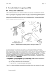
Today, there are a plethora of reasons to conserve energy. These reasons may range from
scarcity of non-renewable energy to scaling down high costs of energy. A common thread
among all of these reasons is the fact that no matter what the source of energy is, there as a
cost associated with using it. As a result, a tremendous amount of research is being
conducted in the realm of energy use reduction. Because cost is a factor in just about every
area of business, the idea is that reducing energy use will reduce costs.
This study targets the relationship between cost ‒ evaluated in dollars, computation power,
etc. ‒ and measures to reduce energy use, or make energy use more efficient. The focus of
this study is how this applies to embedded systems and microcontrollers, which represent a
large portion of all computers in the world today. Although an individual microcontroller
may only consume on the order of milliwatts of energy, the high abundance of
microcontrollers in the world warrants the need for energy efficiency with each
microcontroller. Technology implemented on a small device will have huge impact as it is
then implemented on a large scale.
Specifically, two areas of energy efficiency are explored in this study: (1) Using an algorithm
to achieve the highest power output of a photovoltaic (PV) panel as the input power source to
an embedded system and (2) Using reduced computational digital control to achieve adequate
and correct performance of a buck converter powering peripheral devices. Knowing and
improving the computational requirements of such algorithms gives advantages in two ways.
This means that either (1) a slower, cheaper microcontroller may be used to achieve similar
performance compared to something more expensive, or (2) these computations may be
performed as periodic tasks on the same microcontroller controlling the peripherals. Under
the latter condition, the need to have a separate device to control a buck or boost converter is
eliminated.
1
1.2
Motivation
Since the lifetime of an embedded system is typically several years, the consideration for
having a renewable energy source is an excellent choice. Typical embedded systems that use
non-renewable energy are powered either by batteries or by AC wall power, so two major
tradeoffs with using renewable energy such as a solar PV panel are (1) cost of a PV panel and
(2) availability of input power. Where AC wall power is generally constantly available, and
batteries occasionally need to be charged or replaced, power from PV panels is not always
available due to the inevitable absence of light. This can be compensated by storing the solar
generated energy in a rechargeable battery. However, two additional considerations arise
from doing so: (1) biasing the load to get the maximum power out of the PV panel, and (2)
boosting or compensating the PV panel’s voltage to be sufficient to charge the battery. If the
cost of taking both of these factors into consideration is reduced, then the choice of having a
PV panel as a power source, despite a higher initial cost, can lead to substantial savings in
cost and energy.
In a related concept, both cost and use of energy are important factors to control and be
aware of in an embedded system. When determining an appropriate method of DC-DC load
line regulation in an embedded system, two common approaches typically arise: the use of a
linear regulator or the use of a switching converter. Although linear regulators are cheap
compared to switching converters, they do not come close to matching the efficiency of a
switching converter. Since switching converters are much more efficient, their higher cost
can be justified by the amount of wasted energy they prevent and in turn the amount of cost
saved. A large portion of the cost of a switching converter is the control mechanism used to
regulate DC-DC voltage conversion [1]. A target of research for years has been on reducing
the cost of the control mechanism, and as it is lowered, switching converters become a more
feasible and obvious choice for DC-DC power regulation, especially for embedded systems.
1.3
Background
In both of the areas that this study targets, control and control theory is at the heart of each
concept. Control, typically meaning feedback control, has traditionally been implemented in
analog circuitry. The choice of using analog circuitry has been because of its availability and
2
relative low cost to alternative options. As a result, there are many control systems that exist
in analog circuitry, as well as papers and research that supports using analog methods to
perform feedback control. In the recent years alternative methods ‒ such as digital control ‒
have begun to be as cheap or cheaper than analog methods. As semiconductors and
computer technology have improved, it has become much more feasible to use digital control
in place of analog control. Aside from cost, digital control is (1) flexible and scalable, easy
to change, (2) less sensitive to aging, and (3) less sensitive to noise. Plausible downsides to
using digital control over analog control include (1) round-off and computational error, and
(2) delay in computation, and (3) more complexity in design [6]. However, even taking these
three downsides into account, this study focuses on just how different the performance is
with these are all taken into account.
3
Figure 1. Schematic of Buck Converter Used in this Study
L
D
100 μH
V in
+
NMOS
BD
PWM
C
47μF
ADC in
1Ω
V out
Zener
-
Figure 2. Schematic of Boost Converter Used in this Study
4
For Switched Mode Power Supplies (SMPS) switching converters, analog control feedback
has traditionally been used, but digital control has made a presence in the last decade. Using
digital control is highly justifiable especially for SMPS because of the need for a Pulse Width
Modulation (PWM) signal to control the Duty Cycle (D) for the transistor switches.
Although a PWM signal can easily be generated from analog circuitry, most modern
microcontrollers have the capability to generate a PWM signal without incurring a high
computational cost. Instead of using operational amplifiers and linear components to build a
compensator, a microcontroller simply must use an A/D converter to quantize the output
voltage, perform a computation via a difference equation, and update a register that
automatically takes care of the PWM signal. Therefore, the complexity becomes manifest by
(1) choosing a fast enough microprocessor with an adequate A/D converter, and (2)
designing a digital compensator that will allow the SMPS to meet specifications under
varying conditions.
Figure 3. Power Curve of a Typical Large PV Panel [2]
For a solar PV panel, getting the maximum output power (i.e. maximum solar efficiency) is
achieved by biasing the output voltage and current of the PV panel. This is normally
accomplished by biasing the amount of input impedance that the PV panel sees as a load.
5
The output power then becomes a function of the output voltage, according to the powervoltage curve intrinsic to a solar PV panel. When connecting a buck or a boost converter to a
PV panel, the input impedance becomes a function of many factors, including load resistance
and duty cycle. If all other things are assumed constant, biasing the input impedance of the
switching converter can be done simply by adjusting the duty cycle. Because of the nature of
the power-voltage curve of a PV panel (see Figure 3), there is a maximum power point
achieved at a particular duty cycle value, and Maximum Power Point Tracking (MPPT) is a
method used to control the duty cycle to attain the maximum power. These algorithms have
been proven to be effective, and have traditionally been implemented in combinations of
analog circuitry and digital logic. For similar reasons to those of an SMPS, microcontrollers
now pose as a viable option because of their ability to perform calculations.
A method to achieve optimal efficiency of energy use is by regulating the voltage through
Aggressive Voltage Scaling (AVS). This involves using an SMPS to regulate an output
voltage. The application of AVS to microcontrollers within embedded systems is manifest
by having a microcontroller sample an output voltage and then use a digital compensator in
software to adjust the duty cycle accordingly. The digital compensator is run periodically in
a control loop that can either match the switching frequency of the transistors in the SMPS or
it can run slower to conserve computational power. What this allows for is two things; either
(1) the output voltage can be reduced to the minimum allowed voltage required by the load
that is being powered, with the control loop running as fast as possible to ensure that the
output voltage never dips below this threshold, or (2) the control loop can be run slower to
conserve computational power and the operational voltage is raised a fair amount above the
load’s minimum threshold so that the digital controller will have time to respond and regulate
the voltage if it should drop due to some disturbance [4]. This is based on the fact that with a
time varying load, voltage will naturally drop if current consumed by the load increases.
This also applies to keeping output voltage below a load’s maximum voltage threshold.
What makes AVS aggressive is its ability to use a single microcontroller to handle multiple
voltage domains within a single system. For example, with a single power supply, such as a
6
battery or a PV panel, four voltage domains may be managed, where one domain is boosted
above the input voltage, two may be bucked down below the input voltage, and one may be
bucked to one of the same voltages as another domain, but have tighter constraints and
therefore a more sophisticated digital compensator. Using a single microcontroller is a
different approach to the more prevalent method of giving each individual SMPS its own
dedicated compensator. While using a single microcontroller to regulate multiple power
domains, software timing constraints must also be met because each domain will have its
own dedicated digital compensator running at a different frequency depending on the
constrains for that domain. These software timing constraints can be realized by use of a
Real-Time Operating System (RTOS). Using an RTOS to achieve optimal performance, it is
important to know the computational demand a digital compensator will have, which is
dependent upon the system characteristics and the constraints that must be met for the load.
This study focuses on determining the computational demand for regulating input power
from a PV panel or output voltage for a load based on different constraints.
1.4
Related Work
1.4.1
Use of Microcontrollers for Digital Control in Power Electronics [3]
The advance has been made in the last decade to go from using analog circuitry to control an
SMPS to using a digital compensator. This paper proposes implementing a digital
compensator specifically on a microcontroller (MCU) – as opposed to strict digital logic –
and explores some of the limitations and factors that must be overcome by modeling
traditional analog control theory on a digital scale. A few of the factors that are explored are
(1) MCU clock speed, (2) ADC resolution, (3) ADC conversion time, (4) PWM resolution,
and (5) control loop frequency. Any reduction is control loop frequency relative to the
switching frequency discussed in this paper has more to do with the limitations of the MCU
than it does with intentionally lowering the control loop frequency; the intention was to use
digital control to closely mimic analog control. The conclusions of this paper are that control
implemented on an MCU will (1) ease the design process, (2) allow the control to be
scalable, and (3) reduce the amount of passive components required for control.
7
1.4.2
The Relationship Between Control Loop Frequency and Operating Voltage [4]
In a recent paper, Juneja et al. explored the real-time characteristics of digital control for
SMPS implemented in software on MCUs. The paper involved modeling the behavior of a
particular buck converter, verifying that model by comparing simulation to actual output, and
designing a digital compensator to regulate the output. The paper aims to explore practical
software implementations of digital compensators on an embedded system. Therefore,
different frequencies (other than the SMPS switching frequency) for the control task are
explored, and the effect that varying the frequency has on the closed-loop response is
analyzed. This behavior is embodied in Figure 4.
Figure 4. Impact of Lowering Task Frequency on Transient Response. The black curve displays the open-loop
response, while each colored curve shows the closed-loop response at different task frequencies. The voltage margin,
Vmargin, is defined by how far the voltage falls before compensation. [4]
8
Relationship between Vmargin and ftask
0.6
0.5
Vmargin
0.4
0.3
0.2
0.1
0
0
100
200
300
400
500
Control Loop Frequency, ftask (KHz)
Figure 5. The Relationship Between Vmargin and ftask at a 5 V Operating Point. [4]
It is recognized that many loads are going to have a target minimum and maximum operation
range, Vmax and Vmin, and operation of the load will have to stay within these limits. The
proposed measure of compensation then becomes raising the load’s operating voltage by a
defined voltage margin, Vmargin, which will allow the voltage to fall further with lower task
frequencies when loading, yet keep the operating voltage above Vmin. As long as the voltage
margin does not push the load’s operating voltage above Vmax, the task frequency can be
lowered with a growing Vmargin. Similarly, the load’s operating voltage can be reduced by
Vmargin closer to Vmin so that it will not exceed Vmax when unloading. Figure 5 displays the
relationship between the control loop task frequency and Vmargin.
1.4.3
MPPT Algorithms for Solar PV Panels [2]
Morales [2] did an in depth survey and study of the efficiency of different MPPT algorithms
for PV panels. The survey started by identifying various algorithms that have been the
subject of research for years prior. The survey resulted in identifying three particular
algorithms that were suitable for medium to large PV panels. The first two are called “hillclimbing” methods, and include Perturb and Observe (P&O), and Incremental Conductance
(InCond). The third identified method was Fuzzy Logic Control (FLC). Several other
9
algorithms were proposed as well, including Neural Networks, Constant Fractional
Reference, and Current Sweep.
To be able to test and compare the efficiency of each MPPT algorithm, a simplified
theoretical model was constructed. This simulation was intended to model actual sunlight
conditions, which include increases and decreases in both solar irradiation and temperature.
To compare additional details of each of the algorithms’ performance, factors about the
simulation were varied between runs, for example, the irradiation gradient over time.
The findings were that efficiency must be measured on more than just a simple percentage.
Efficiency of an MPPT algorithm is also characterized by how well and how quickly the
algorithm responds to changes in temperature and irradiation. As far as each algorithm’s
efficiency, the two that performed the best were the P&O and InCond methods. The FLC
algorithm performed well, but did not outperform either of the more simple “hill-climbing”
methods, P&O or InCond, so it was concluded that the extra cost in performance did not
justify the complexity of logic. Using a modified P&O algorithm that included extra rules
was determined to be better than the FLC control. The simulations indicated that both hill
climbing algorithms were able to achieve around 99% efficiency.
1.5
Outline of the Rest of the Document
The rest of the document will proceed in this order. Chapter 2 discusses the theoretical
impact of relaxing some of the constraints of digital control theory targeting reduced
computational demand. Chapter 3 discusses the computational impact of using various
MPPT algorithms to achieve maximum output power of a PV panel. Chapter 4 discusses the
computational impact of different methods of relaxed digital control. Chapter 5 is a
collaboration of results and a final discussion on the significance of these findings.
10
2.
Relaxing Constraints of Digital Control Theory
2.1
The Nyquist Sampling Theorem
When adding a sampler (analog-to-digital converter) and a signal reconstructor (digital-toanalog converter) to an analog line, the Nyquist Sampling Theorem states that a sampled
signal can be reconstructed perfectly if it is sampled at a rate that is twice the highest
frequency present in the sampled signal [5]. This is to say that if the highest frequency in a
signal is known, the sample rate should be chosen to be at least double that frequency to
prevent signal corruption on the output side. This is a necessary constraint for digital signal
processing and typically for digital control. However, when using digital control to control
an SMPS, there is no interest in recreating an output signal. The only necessity is that a
PWM signal is generated to control the switching transistors of the SMPS. This provides
justification for exploring the impact of reducing the sampling rate below what the Nyquist
Sampling Theorem mandates.
2.2
Slowing Down the Sampling Rate
One of the limitations of a microcontroller is how fast it can run. Ideally, a system could
receive input, process it, and send it out with no delay, which is a characteristic of an analog
system. However, since a microcontroller is being used, what is being gained in scalability is
being lost in instantaneity, and the speed at which data is processed must be considered. The
sample rate can be chosen according to the Nyquist Sampling Theorem, but several
constraints may be relaxed because the signal is not being sampled with the intent of
reconstruction. Since the SMPS being used in this case is a DC-DC converter, the first
assumption that can be made is that the signal is primarily a DC signal, and higher
frequencies can be ignored and are not the focus of control. The following figures show the
characterization of typical DC loads.
11
Figure 6a. Voltage and Current Response to a Servomotor making a full turn.
Figure 6b. Voltage and Current Response to a Step Load of 10Ω
Figure 6. Characterization of Typical DC Loads. Both graphs are voltage response to a sudden increase in load
current draw. The top curve for each represnets the voltage, and the bottom curve represents the current.
DC loads tend to be characterized by sudden changes in voltage due to current consumption
shooting up or down. These sudden changes in voltage are the primary focus of control, so
for this reason, the sample rate must be high enough to prevent the voltage from falling too
low or raising too high. Traditionally, the sample rate of the output voltage is set to the
switching frequency of the converter. There is little justification for it to be any higher than
the switching frequency, because since the PWM signal is purely digital, it can only take a
single value per period. For this reason, the maximum sampling rate need not be any higher
12
than the switching frequency, so the each new value of D is based on each new sample of the
output voltage.
If the digital compensator is implemented in a microcontroller as a periodic task, the
sampling rate of the output signal determines the task frequency. Higher task frequency on a
microcontroller has one of two implications: (1) higher utilization on a processor running
many periodic tasks, or (2) less time in sleep mode for a processor trying to conserve power.
In either of these cases, there is value gained in lowering the tasking frequency, and
consequently lowering the sampling frequency. If the performance of the digital
compensator can still be favorable with a reduced sampling rate, then relaxing these
constrains becomes beneficial.
Referring to Figure 6a and Figure 6b, the output voltage drops when the device turns “on.”
The goal of the compensator is to keep the output voltage constant regardless of how often
the device turns on or off. As described by [4], how much the voltage falls before being
compensated and brought back up is related to how fast it is being compensated. Therefore,
one method for setting the sampling rate of a DC-DC converter is based on the maximum and
minimum allowed voltages for a device around the reference operating voltage.
Another constraint that can be relaxed has to do with the fact that the signals are primarily
DC signals. A majority of the time, a signal will be in steady-state, held at a certain voltage.
Only less frequently does the current change dramatically. For this reason, it is reasonable to
change the sample rate dynamically based on being in steady-state or oscillation. While the
signal is primarily in steady-state mode, the sample rate can be much lower, but as soon as
the voltage begins to drop or rise due to change in current, the signal can switch to
emergency mode and the sample rate can increase to quickly compensate the signal back to
steady-state mode. Being able to switch between steady-state mode and emergency mode
allows for the control task utilization to only infrequently be high.
13
2.3
Impact of Slowing Down the Sampling Rate
Appendix B details how to construct a linear model of a DC-DC converter plant for an
otherwise nonlinear system. Using the linear model around a quiescent operating point, the
system can be treated as a plant that can be controlled using traditional feedback closed
control loops. Figure 7 shows the linearized AC equivalent small-signal model of the DCDC converter. Figure 8 shows the block diagram of the DC-DC converter as a linear system,
and Eqns (1) and (2) show the transfer functions of the resulting system.
Figure 7. Small Signal AC Equivalent Model of Buck Converter
Figure 8. System Block Diagram of Buck Converter
14
𝐺𝑣𝑑 (𝑠) =
𝐺(𝑠) = �
4.9 ×
0.000282𝑠 + 10
+ 5.064 × 10⁻⁵ 𝑠 + 1
10−9 𝑠 2
1 − 𝑒 −𝑠𝑡 −3.5×10⁻⁶ 𝑠
0.000282𝑠 + 10
�𝑒
−9
𝑠
4.9 × 10 𝑠 2 + 5.064 × 10⁻⁵ 𝑠 + 1
(1)
(2)
This system, typical of a common power electronics system, is unlike traditional closed-loop
feedback systems because the input to the control loop is actually just a reference voltage,
and the actual input voltage to the system that is either being boosted or bucked is treated as a
disturbance near the output of the system. This is also true of the load, which fluctuations in
both the load and the input voltage are treated as disturbances that need to be compensated
via changes in the duty cycle. Note the difference between the control-to-output transfer
function, Gvd(s), and the plant transfer function, G(s), which includes a zero-order hold
(ZOH), the delay imposed by using a microcontroller, as well as transfer gains, which
ultimately all equate to 1 when multiplied together. The z-domain transform of the plant
transfer function is shown in Eqn (3), and is acquired by using an s-plane to z-plane mapping
of 𝑧 = 𝑒 𝑠𝑇 , where the sampling period T is the inverse of the sampling frequency of 150
kHz.
𝐺(𝑧) = 𝑧 −1
0.1975𝑧 2 + 0.08058𝑧 − 0.1868
𝑧 2 − 1.922𝑧 + 0.9307
(3)
Eqn (1) shows the bode plot of the control-to-output transfer function (Gvd(s)), Eqn (2) shows
the plant transfer function (G(s)), and Eqn (3) shows the transformed z-domain transfer
function (G(z)). The bode plot in Figure 9 demonstrates the effect of the delay on the phase
of the transfer function, as well as the effect of sampling the transfer function. The bode
diagram here for the sampled z-domain transfer function cuts off at half the sampling
frequency, or the Nyquist frequency; beyond this frequency, the graph is periodic. Although
the graphs differ in high frequency behavior, they are primarily the same over the lower span
of typical operating frequencies, including the corner frequency.
15
Bode Diagram
40
Gvd
Magnitude (dB)
20
Gs
Gz
0
-20
-40
-60
Phase (deg)
-90
-180
-270
-360
0
10
1
10
2
10
3
10
Frequency (kHz)
Figure 9. Bode Plots of Plant Transfer Functions
Because the output signal is primarily a DC signal, it is possible to lower the sampling rate
down below the converter switching frequency without a tremendous amount of data
corruption. Several lower sampling frequencies were chosen, and Figure 10 shows the
impact that the lower sampling frequencies have on the bode plot of the transfer function
G(s).
16
f = 150 kHz
f = 100 kHz
Bode Diagram
40
f = 75 kHz
f = 50 kHz
f = 25 kHz
Magnitude (dB)
20
f = 10 kHz
f = 5 kHz
0
-20
-40
0
Phase (deg)
-90
-180
-270
-360
-2
10
-1
10
0
10
1
10
2
10
Frequency (kHz)
Figure 10. G(s) Sampled at Various Frequencies
For each of the sampling frequencies present in Figure 10, the bode plot of the transfer
function cuts off at half the sampling frequency, or the Nyquist frequency. For the part of the
plot that exists before the Nyquist frequency cutoff, each plot continues to resemble the
original plot of the continuous-time plant transfer function G(s). Only when the sampling
frequency reduces so low that the Nyquist frequency cuts off the plot’s corner frequency does
the sampled plant transfer function no longer bear resemblance to the original plant transfer
function.
Another interesting effect that lowering the sampling rate has is on the movement of the
poles and zeros of the plant transfer function. Figure 11 shows the open-loop poles of the
plant. Figure 12 shows the movement of the poles with reducing the sampling rate. They
move along a constant-zeta line, while what is reduced is the relative undamped natural
frequency, which is based on the sampling period T (the reciprocal of the sampling
frequency). Figure 13 shows the z-plane grid within the unit circle of stability.
17
Pole-Zero Map
1
Pole-Zero Map
1
0.8
0.8
0.6
0.6
0.4
0.4
0.2
f = 150 kHz
f = 100 kHz
f = 75 kHz
f = 50 kHz
Imaginary Axis
f = 25 kHz
Imaginary Axis
0.2
0
0
-0.2
-0.2
-0.4
-0.4
-0.6
-0.6
-0.8
-0.8
-1
-1.5
f = 10 kHz
f = 5 kHz
-1
-1.5
-1
-0.5
0
0.5
1
Real Axis
-1
-0.5
0
0.5
1
Figure 12. Movement of Poles and Zeros with Changed
Sampling Frequency
Real Axis
Figure 11. Open-Loop Poles and Zeros of the Plant
Pole-Zero Map
1
0.8
0.6π/T
f = 150 kHz
f = 100 kHz
0.5π/T
0.4π/T
0.10.3π/T
0.7π/T
0.2
f = 75 kHz
0.6
f = 25 kHz
0.4
0.3
0.4
0.5
0.6
0.7
0.8
f = 50 kHz
0.8π/T
f = 10 kHz
f = 5 kHz
0.9π/T
Imaginary Axis
0.2
0
0.2π/T
0.1π/T
0.9
1π/T
1π/T
-0.2
0.9π/T
0.1π/T
-0.4
0.8π/T
-0.6
0.2π/T
0.7π/T
-0.8
0.3π/T
0.6π/T
-1
-1.5
-1
-0.5
0.5π/T
0
0.4π/T
0.5
1
Real Axis
Figure 13. Z-plane Grid with Lines of Constant Damping and Constant Natural Frequency
18
What Figure 12 helps make clear is that the characteristics of the plant – which come from
the plant’s continuous-time characteristic equation – stay the same despite changing the
sampling rate. The characteristic equation of a second-order continuous-time transfer
function takes the form
𝑠 2 + 2𝜁𝜔𝑛 𝑠 + 𝑤𝑛2 = 0
(4)
and from this, the damping factor and undamped natural frequency can be determined.
Figure 14 shows the same movement of the poles as Figure 12, but along the specific
damping factor line, ζ = 0.3693, and through lines of constant undamped natural frequencies,
ωn = 1.46 × 10⁴ radians/sec. The lines of undamped natural frequency represented in Figure
13 and Figure 14 are calculated by
𝜔𝑧 =
𝜋𝑓𝑛 𝜔𝑛
=
𝑓𝑠
𝑓𝑠
(5)
Only when the sampling frequency becomes too low does the system become altered to the
point where its characteristic equation no longer represents the same system. This is
demonstrated first by Figure 10, where the corner frequency of the bode plot is essentially cut
off due to such a low sampling frequency of 5 kHz, and again in Figure 14, where the
movement of the zeros becomes odd. Above the sampling frequency of 10 kHz, both zeros
move in towards z = 0. Around and below the sampling frequency of 10 kHz, the left zero on
the z-plane begins to again move away from the z = 0 point. The z-plane relativity of poles
and zeros no longer holds at such low sampling frequencies.
19
Pole-Zero Map
1
0.8
0.6
0.292
1.46
f = 150 kHz
f = 100 kHz
0.194
f = 75 kHz
0.369
f = 50 kHz
0.146
0.583
f = 25 kHz
Imaginary Axis
0.4
0.0972
f = 10 kHz
f = 5 kHz
0.2
0.292
2.92
0.369
0.194
0.146
0.0972
0
0.0972
0.146
0.194
2.92
-0.2
0.0972
0.292
0.146
-0.4
0.583
0.194
-0.6
-0.8
-1
-1.5
0.292
0.8
1.46
-1
-0.5
0
0.5
1
Real Axis
Figure 14a. Full View of Graph
0.9
1
Figure 14b. Closer View of Graph
Near z = 1
Figure 14. Z-plane Grid of Plant Transfer Function Poles and Zeros
As long as the sampling frequency stays high enough above the corner frequency, the
sampling rate can be reduced enough to slow the control task frequency down yet continue to
model the same system.
2.4
Modeling Continuous Domain Transfer Functions in the Discrete
Domain
Typical design procedures for digital compensators involve design in the continuous domain.
In the end, most systems operate in the continuous domain, even if a system involves a
sampler. When going from the continuous domain to the discrete domain, several methods
may be employed. The method used to take the plant transfer function G(s) from the
continuous domain to the discrete domain to produce G(z) used a Zero-Order Hold (ZOH)
along with a mapping of 𝑧 = 𝑒 𝑠𝑇 . This involves defining a modified version of a transfer
function H(s) as H*(s), which is a version of H(s) that is only defined at discrete intervals of
� (𝑠), which
the sampling period T. A zero-order hold is then applied to H*(s), resulting in 𝐻
is defined over all time, and takes the discrete values of H*(s) and holds them over each
20
� (𝑠) where z = esT. In a single
interval span of length T. H(z) is then just evaluated from 𝐻
equation, the transformation of h(t) to H(z) using the ZOH method is
∞
𝐻(𝑧) = �� ℎ(𝑘𝑇)𝑒 −𝑘𝑇𝑠 � �
𝑘=0
1 − 𝑒 −𝑠𝑇
�
𝑠
𝑒 𝑠𝑇 =𝑧
(6)
Phillips and Nagle [6] make a good argument for doing compensator design in the w-plane
over the s-plane. The reasoning is that the w-plane to z-plane mapping is very simple and
hardly loses any precision, and relatively low pole frequencies in both the s-plane and wplane are nearly identical. The s-plane to w-plane mapping can be described by
𝜔𝑤 =
where w = jωw and s = jωs. When
2
𝜔𝑠 𝑇
tan
𝑇
2
𝜔𝑠 𝑇
2
(7)
≪ 1, ωw ≈ ωs. This mapping comes in handy
especially for design of PID controllers in the w-plane. In the w-plane, a PID controller may
take the form shown in Eqn (8).
𝐷(𝑤) = 𝐾𝑃 +
𝐾𝐼
+ 𝐾𝐷 𝑤
𝑤
(8)
This uses s-plane integrator and differentiator relationships. When designed in the w-plane, a
PID controller may be designed irrespective of the sampling period T. With this design, a wplane compensator may be mapped to a z-plane function using trapezoidal integration and
trapezoidal differentiation, which both come from approximations of 𝑧 = 𝑒 𝑠𝑡 . Eqn (9) shows
the w-plane to z-plane mapping for a trapezoidal integrator and a trapezoidal differentiator:
Trapezoidal Integrator
1 𝑇𝑧+1
=
𝑤 2𝑧−1
Trapezoidal Differentiator
𝑧−1
𝑤=
𝑧𝑇
(9)
This method of designing a z-plane PID compensator in the w-plane is arguably preferred
over the brute-force method of z-plane PID compensator design, where differentiation and
integration of the signal are done numerically in the discrete domain, and the values of KP,
21
KI, and KD are applied to the proportional, integral, and differential parts of the fed back
signal. The brute force method is demonstrated in Figure 15.
Numerical
Integrator
KI
E(z)
Σ
KP
M(z)
Numerical
Differentiator
KD
Figure 15. Block Diagram of a Numerical PID Compensator
Alternatively, designing a z-plane PID compensator in the w-plane will always result in a
transfer function in the form
𝐷(𝑧) =
𝑎0 𝑧 2 + 𝑎1 𝑧 + 𝑎2
𝑧(𝑧 − 1)
(10)
where a0, a1, and a2 are expressed by the relationships:
𝐾𝐼 𝑇 𝐾𝐷
+
2
𝑇
𝐾𝐼 𝑇
2𝐾𝐷
𝑎1 =
− 𝐾𝑃 −
2
𝑇
𝐾𝐷
𝑎2 =
𝑇
𝑎0 = 𝐾𝑃 +
(11a)
(11b)
(11c)
When implemented on a digital compensator, the transfer function becomes a very simple
second-order difference equation:
𝑑[𝑛] = 𝑑[𝑛 − 1] + 𝑎0 𝑒[𝑛] + 𝑎1 𝑒[𝑛 − 1] + 𝑎2 𝑒[𝑛 − 2]
22
(12)
This method of PID control, which involves three multiplications and three additions,
becomes much less computationally demanding on the microcontroller compared to the brute
force method, which would involve additional multiplications and additions due to numerical
integration and differentiation of the signal.
2.5
Impact of Slowing Down the Sampling Rate of a Digital Compensator
Referring to the block diagram in Figure 8, the buck converter with continuous-domain
transfer function G(s) described in Eqn (2) and discrete-domain transfer function G(z) in Eqn
(3) can be applied a digital PID controller designed in the w-plane in the form:
𝐷(𝑤) = 0.9177 +
10000
+ 8.284 × 10⁻⁶ 𝑤
𝑤
(13)
Using the sampling frequency equal to the buck converter’s switching frequency of 150 kHz,
this maps to the z-plane using the relation in Eqn (9):
𝐷(𝑧) =
2.193𝑧 2 − 3.368𝑧 + 1.242
𝑧2 − 𝑧
(14)
This results in a compensated bode plot with phase margin and gain margin values displayed
in Figure 16 and the root locus in Figure 18 shows the movement of closed loop poles over
different open-loop gain values. Closed-loop gain values near 1 are chosen on the root-locus
diagram to show where the closed-loop poles will end up for a gain of 1. Note that only two
of the closed-loop poles are shown because all imaginary poles are reflexive in a real-valued
system [7]. Figure 17 additionally shows the step response of the system. The step response
models a step-input of VREF changing immediately from 0 V to 1 V.
23
Bode Diagram
Gm = 7.34 dB (at 43.7 kHz) , Pm = 67.5 deg (at 12.6 kHz)
Step Response
1.4
60
Gz
Magnitude (dB)
Gz*Dz
Gz
40
1.2
Gz*Dz
20
1
0
Amplitude
-20
-40
0
0.8
0.6
Phase (deg)
-90
0.4
-180
0.2
-270
0
-360
-1
10
0
1
10
2
10
10
0
0.5
1
1.5
2
2.5
Time (seconds)
Frequency (kHz)
Root Locus
System: untitled1
Gain: 0.948
Pole: -0.0389 + 0.572i
Damping: 0.322
Overshoot (%): 34.4
Frequency (rad/s): 2.59e+05
1
Imaginary Axis
0.5
0
System: untitled1
Gain: 0.948
Pole: 0.828 - 0.178i
Damping: 0.617
Overshoot (%): 8.52
Frequency (rad/s): 4.04e+04
-0.5
-1
-2
-1.5
-1
3.5
-0.5
0
0.5
1
1.5
Real Axis
Figure 18. Root Locus of Compensated System with Closed Loop Gains Close to 1 Chosen
24
-4
x 10
Figure 17. Step Response of Uncompensated and
Compensated Systems
Figure 16. Bode Diagram of Uncompensated and
Compensated Systems with Phase Margin and Gain
Margin Displayed
-2.5
3
This specific PID compensator was chosen after much tuning and accomplishes several
things. First, it eliminates steady-state error to a step. Figure 17 shows that the
uncompensated system step response will not settle to a value equal to the step it received.
Adding the compensator eliminated the steady-state error because it turns the system into a
Type-I system. A Type-N system is defined by how many powers of (𝑧 − 1)𝑁 are in the
denominator in the z-domain, or how many powers of 𝑠 𝑁 or 𝑤 𝑁 are in the denominator in the
s-domain or w-domain. By proof [6], all Type-I systems have 0% steady-state error to a step.
Using the method described in Eqns (8), (9), and (10), all PID compensators will always be
of Type-I because they will always have at least one single power of (𝑧 − 1) in the
denominator. This is one reason the choice of a PID compensator is optimal. Another thing
the PID compensator accomplishes is reducing overshoot while keeping the rise time fast,
which is also demonstrated in Figure 17. This comes from proper tuning of the PID
controller.
When reducing the sampling frequency of the plant, this alters the behavior of the digital
controller, which is designed for a specific sampling period, T. That is, the digital controller
D(z) is mapped to the z-plane from the w-plane based on a specific sampling period, T. Two
natural choices for a design decision arise from lowering the sampling frequency: (1) derive
different PID compensators for different values of T based on the same w-plane PID
compensator, or (2) use the same PID compensator designed for a specific value of T and
verify that it still behaves favorably at greater values of T (i.e. lower sampling rates). The
first method is a method of pseudo-adaptive control, which means that the transfer function
changes dynamically. It is however only pseudo-adaptive because it involves modeling the
same w-plane PID compensator, but calculating different values of a0, a1, and a2 (see Eqn
(11)) for different sampling frequencies.
Although using a digital compensator designed for one sampling frequency at a different
sampling frequency is not a traditionally accepted method, the effect that lowering the
sampling frequency has on a digital controller is notable. The effect that lowering the
25
sampling frequency has can be modeled in three different ways: (1) the effect on the bode
plot, (2) the effect on the step response, and (3) the effect on the system’s poles and zeros.
f = 150 kHz
Bode Diagram
100
f = 100 kHz
f = 75 kHz
Magnitude (dB)
f = 50 kHz
f = 25 kHz
50
f = 10 kHz
f = 5 kHz
0
-50
90
Phase (deg)
0
-90
-180
-270
-360
-3
10
-2
10
-1
0
10
10
1
10
2
10
Frequency (kHz)
Figure 19. Bode Plot of System at Different Frequencies
Table 1. System Gain Margins and Phase
Margins at Various Sampling Frequencies.
“Inf” implies no -180° crossing for the phase
margin.
Sampling
Frequenc
y
150 kHz
100 kHz
75 kHz
50 kHz
25 kHz
10 kHz
5 kHz
Gain
Margin
Phase
Margin
7.34 dB
6.35 dB
4.94 dB
-1.65 dB
-10.4 dB
-22.7 dB
-35.7 dB
67.5°
57.2°
31.4°
Inf
Inf
Inf
Inf
26
Step Response
1.5
f = 150 kHz
f = 100 kHz
f = 75 kHz
Amplitude
1
0.5
0
0
1
3
2
4
5
6
Time (seconds)
7
-4
x 10
Figure 20. System Step Responses at Different Sampling Frequencies
What Table 1 shows is that for decreasing the sampling frequency, the phase margin also
decreases for this PID compensated system, until the phase margin disappears, which is listed
as “Inf” for infinity. The phase margin is directly related to the damping factor, ζ, by the
equation:
𝜁=
sin 𝜙𝑀
2�cos 𝜙𝑀
(15)
The percent overshoot is in turn directly related to ζ by the equation:
%𝑂. 𝑆. = 𝑒
−𝜁𝜋
�1−𝜁2
× 100%
(16)
As the phase margin decreases, the damping factor decreases as well, moving the system
closer to oscillation. This is displayed in Figure 20, as the percent overshoot increases with
decreased sampling frequency, and the system oscillates more in response to a step. Figure
20 does not display step responses to sampling frequencies below a sampling frequency of 75
kHz, because those systems are unstable.
27
Since the digital compensator represents the same z-plane poles and zeros for changing
values of T, the effect that changing the sampling frequency has on the poles and zeros must
be looked at in the w-plane. As Eqns (8), (9), and (10) detail how to go from the w-plane to
the z-plane, going from the z-plane to the w-plane can be solved by reversing the process.
Eqn (17) transforms the relationship that a0, a1, and a2 have to KP, KI, KD, and T into a matrix
equation, and Eqn (18) represents the solution to that equation.
𝑇
⎡1 2
⎢−1 𝑇
⎢
2
⎢
⎣0 0
1
𝑇 ⎤ 𝐾𝑃
2
−𝑇⎥⎥ � 𝐾𝐼 �
1 ⎥ 𝐾𝐷
𝑇 ⎦
⎡1
𝐾𝑃
� 𝐾𝐼 � = ⎢⎢−1
⎢
𝐾𝐷
⎣0
𝑇
2
𝑇
2
0
𝑎0
= �𝑎1 �
𝑎2
1 −1
𝑇 ⎤
𝑎0
2⎥
−𝑇⎥ �𝑎1 �
𝑎2
1 ⎥
𝑇 ⎦
(17)
(18)
From Eqn (8), a pole-zero form of a w-plane PID compensator transfer function may be
derived:
𝐾𝐷 𝑤 2 + 𝐾𝑃 𝑤 + 𝐾𝐼
𝐷(𝑤) =
𝑤
(19)
Using the relationships in Eqns (18) and (19), and values for a0, a1, and a2 from Eqn (14) of
2.193, -3.368, and 1.242 respectively, the w-plane poles and zeros can be equated. Figure 21
displays how the w-plane poles and zeros move as the sampling period, T changes. What
Figure 21 reveals is that the zeros are the only factors of the transfer function that move, and
they move linearly with T away from w = 0. Based on Eqn (19), all sampling frequencies
that D(w) is calculated for will have one pole at w = 0, irrespective of the sampling period.
The sampling frequency alone will never turn the PID controller itself into an unstable
controller, however, the simulations indicate that the sampling frequency still has impact on
the entire system.
28
w -plane
0.2
f = 150 kHz
0.15
f = 100 kHz
f = 75 kHz
f = 50 kHz
Imaginary Axis (seconds-1)
0.1
f = 25 kHz
f = 10 kHz
0.05
f = 5 kHz
0
-0.05
-0.1
-0.15
-0.2
-10
-8
-6
-4
-1
)
Real Axis (seconds
-2
0
2
-8000
-6000
-4000
-2000
0
4
x 10
Figure 21a. Full View of the Poles and Zeros on the w-plane
Figure 21b. Zoomed View near w = 0
Figure 21. W-plane Poles and Zeros of the PID Compensator with Changing Sampling Frequency
What all of this data suggests is that it is possible to use a digital PID compensator design for
one sampling frequency at lower sampling frequencies up to a certain point. Once the entire
system’s phase margin becomes nonexistent, the system goes unstable. Though the bode plot
suggests different behavior around the corner frequency as the sampling frequency is
lowered, the low-frequency behavior is still similar for lower sampling frequency, which is
important for loads operating in steady-state DC mode. When applying this principle to a
microcontroller, if the output voltage is being sampled in different frequency modes – for
example, steady-state mode and emergency mode – then the amount of oscillation and the
degree of overshoot that occurs is based on the amount of time it takes to switch between
modes, from a slower sampling rate to a quicker sampling rate. This means that as long as
the output voltage is in steady-state, the system can run at a sample at a lower frequency and
use the same transfer function as when the system samples at a higher frequency to
29
compensate for changes in output voltage. Though this is a different approach than standard
digital control theory warrants, it saves in computational and implementation cost.
2.6
Integer Approximation
2.6.1
Integer Arithmetic versus Floating-Point Arithmetic
Often the goal in mathematical modeling is to achieve as much precision as the platform
warrants. This ensures that the mathematical systems model real life systems as close as
possible. In these cases, loss of precision can result in corruption of data, and a mathematical
model that inaccurately models a real life system. For instance, the transfer function in Eqn
(20) represents a Chebyshev Type-II high-pass filter designed to eliminate signal drifting or
wandering.
𝐻(𝑧) =
0.9374 − 4.6828𝑧 −1 + 9.3609𝑧 −2 − 9.3609𝑧 −3 + 4.6828𝑧 −4 − 0.9374𝑧 −5
1 − 4.866𝑧 −1 + 9.4778𝑧 −2 − 9.2363𝑧 −3 + 4.5034𝑧 −4 − 0.8789𝑧 −5
(20)
The z-plane graphing of the poles and zeros of this transfer function results in the graph in
Figure 22.
30
z-plane
1
0.8
0.6
Imaginary Part
0.4
0.2
0
-0.2
-0.4
-0.6
-0.8
-1
-1
-0.5
0
Real Part
0.5
0.94 0.96 0.98
1
Figure 22a. Full z-plane Unit Circle View of the Poles and Zeros
1
1.02 1.04
Figure 22b. Zoomed In View of the
Graph
Figure 22. Z-plane Graph of Poles and Zeros of High-Pass Filter H(z)
In this transfer function, the poles and zeros are extremely close to the point z = 1. This
allows for only the lowest frequencies to be attenuated. The z coefficients in H(z) are
actually condensed versions of the coefficients. Table 2 lists the actual precise coefficients,
where an and bn correspond to anz-n denominator coefficients and bnz-n numerator
coefficients.
Table 2. Coefficients of High-Pass Filter H(z)
b0
b1
b2
b3
b4
b5
0.937482248528358
-4.682785333663319
9.360949324688169
-9.360949324688171
4.682785333663323
-0.937482248528359
31
a0
a1
a2
a3
a4
a5
1.000000000000000
-4.866051787992316
9.477802313600998
-9.236291867014341
4.503414878846232
-0.878872966305784
When the same transfer function is implemented with the same coefficients rounded to four
decimal places, the behavior of the transfer function changes drastically, and the z-plane
poles and zeros move quite noticeably. This is demonstrated in Figure 23.
pa e
z-plane
1
0.8
0.6
Imaginary Part
0.4
0.2
3
3
0
-0.2
-0.4
-0.6
-0.8
-1
-1
-0.5
0
Real Part
0.5
1
Figure 23a. Full z-plane Unit Circle View of the Poles and Zeros
0.9
0.95
1
1.05
Figure 23b. Zoomed In View of the
Graph
Figure 23. Z-plane Graph of Poles and Zeros of Truncated High-Pass Filter H(z)
This behavior may be surprising, because rounding to four decimal places may seem to be an
appropriate amount of rounding to maintain precision. However, the zeros have moved
closer in to z = 1, and two of the poles have even moved outside of the unit circle, rendering
the filter completely unstable. Two factors that a responsible for this are (1) because the
poles are so close to the right edge of the unit circle, z = 1, and (2) because the filter is a
relatively high-order transfer function. In a second-order system where the poles are further
from the z = 1 point on the unit circle, this level of precision is not required. Figure 24 shows
a graph of the poles and zeros on the z-plane of the z-transformed buck converter plant
transfer function. The graph overlaps the poles and zeros of different decimal precisions.
32
Pole-Zero Map
No Rounding
0.8
4 Digits
3 Digits
0.6
2 Digits
Imaginary Axis
0.4
0.2
0
-0.2
-0.4
-0.6
-0.8
-1
-0.5
0
0.5
1
Real Axis
Figure 24a. Full View of z-plane Poles and Zeros
Pole-Zero Map
0.1
No Rounding
4 Digits
3 Digits
0.08
2 Digits
0.06
Imaginary Axis
0.04
0.02
0
-0.02
-0.04
-0.06
-0.08
-0.1
0.75
0.8
0.85
0.9
0.95
1
1.05
Real Axis
Figure 24b. Zoomed in View of z-plane at z=1
Figure 24. Effect of Loss of Precision on Poles and Zeros of Plant Transfer Function
33
As Figure 24 shows, the effect of loss of decimal precision on the poles and zeros of the plant
transfer function is minimal and essentially negligible, especially compared to the effect it
has on the sixth-order high-pass filter. The movement of the poles and zeros based on the
loss of precision is somewhat arbitrary, and depends on the base in which the precision is lost
– which in this case is base ten – and what the polynomial factors to, which is directly what
the poles and zeros come from.
Another conclusion that Figure 24 leads to is that in this case, floating-point precision is not a
strong requirement. This opens the door to other methods of calculation that may not as
computationally intensive as floating-point arithmetic. Because modern microcontrollers
tend to operate on a single chip (excluding peripherals), only high-end, more expensive
microcontrollers will include a Floating-Point Unit (FPU) implemented in hardware to
perform floating-point calculations. Since this study focuses on more cost effective MCUs
that tend to lack FPUs, floating-point arithmetic is typically done in software. The following
figure demonstrates what a floating-point multiplication becomes in terms of instructions on
the RL78 MCU:
Voltage
027FC
027FF
02800
02802
02803
02806
0280E
02811
02812
02815
= ADC_value
AF2EF0
12
31FF
33
FDE104
FD4C05
BF3EF0
13
BF40F0
12
* V_PER_BIT;
MOVW
AX, N:ADC_value
MOVW
BX, AX
SARW
AX, 15
XCHW
AX, BC
CALL
N:?F_SL2F
CALL
N:?F_MUL
MOVW
N:Voltage, AX
MOVW
AX, BC
MOVW
N:0xF040, AX
MOVW
BC, AX
Subroutine
F_SL2F
#
Subroutines
Instr. Called
WRKSEG_PUSH_L09
57
F_MUL
331
WRKSEG_PUSH_L09
48
48
39
22
25
WRKSEG_POP_L09
MOVE_LONG_L06
__fmthrr
_matherr
WRKSEG_POP_L09
WRKSEG_PUSH_L09
WRKSEG_POP_L09
__fmthrr
MOVE_LONG_L06
MOVE_LONG_L06
_matherr
-
Figure 25. Excerpt from RL78 Assembly of a Floating-Point Multiplication. In the table on the left, the four columns
indicate (1) the instruction address, (2) the instruction opcode, (3) the instruction, and (4) the operands. The table on
the right indicates for each subroutine the number of instructions in the subroutine and which additional subroutines
it calls.
34
This operation thus takes on two steps: (1) signed long to floating-point (F_SL2F), and (2),
floating-point multiplication (F_MUL). As displayed in Figure 25, the first operation,
F_SL2F calls two additional subroutines within it, WRKSEG_PUSH_L09 and
WRKSEG_POP_L09, each adding instruction cycles to the length of the original F_SL2F
subroutine. Then the F_MUL subroutine, which is 331 instructions long, operates as a
complex web of loops such that the amount of cycles taken depends each time on the
operands given for multiplication. F_MUL also calls the WRKSEG_PUSH_L09 and
WRKSEG_POP_L09 subroutines, as well as one other subroutine, __fmthrr, which also calls
_matherr. All together, floating-point multiplication is a computationally expensive
operation when it is required to be done in software.
On the same MCU, the RL78, integer arithmetic is significantly less costly. The RL78 is a
16-bit MCU, so doing 8-bit times 8-bit multiplication to result in a 16-bit product may be
handled by a single instruction. This may take one to two clock cycles, according to the
RL78’s software manual [9]. However, 16-bits is a more standard word length, so integer
multiplication will more practically be 16-bit times 16-bit multiplication resulting in a 32-bit
product. As the RL78 has a 16-bit word length, 16-bit by 16-bit multiplication is
implemented in software. The following figure demonstrates what 16-bit multiplication
becomes in terms of instructions on the RL78 MCU:
power_32[0] = voltage_16[0] * current_16[0];
02932
AF68F0
MOVW
AX, N: 0xF068
02935
C1
PUSH
AX
02936
AF66F0
MOVW
AX, N:current_16
02939
C1
PUSH
AX
0293A
DB60F0
MOVW
BC, N:0xF060
0293D
AF5EF0
MOVW
AX, N:voltage_16
02940
FD2F09
CALL
N:?L_MUL_L03
02943
BF6EF0
MOVW
N:power_32, AX
02946
13
MOWV
AX, BC
02947
BF70F0
MOVW
N:0xF070, AX
0294A
12
MOVW
BC, AX
Subroutine
# Instr.
Subroutines
Called
L_MUL_L03
83
-
Figure 26. Excerpt from RL78 Assembly of an Integer Multiplication. In the table on the left, the four columns
indicate (1) the instruction address, (2) the instruction opcode, (3) the instruction, and (4) the operands. The table on
the right indicates for each subroutine the number of instructions in the subroutine and which additional subroutines
it calls.
35
Although the multiplication still must be done via a call to a subroutine, the long integer
multiplication (L_MUL_L03) subroutine only involves a single loop, which iterates far fewer
times compared to the complex network of loops in the F_MUL subroutine.
Although it is a generally accepted idea that software integer multiplication requires
significantly less instruction cycles than software floating-point multiplication, Table 3
points out just how much the advantage is specifically for the RL78 platform. This study in
Chapter 3 and Chapter 4 will show the impact of reduction of precision in calculations.
Table 3. Comparison of Number of Instructions Required for Integer
and Floating-Point Multiplication
Method
Number of Instructions
Integer Multiplication
94
Floating-Point Multiplication 793
2.6.2
Integer Arithmetic versus Fixed-Point Arithmetic
Fixed-point arithmetic tends to offer a feasible solution to resolving computational demand
compared to floating-point arithmetic. [8] details the operation of fixed-point arithmetic,
which is summarized in Table 4.
36
Table 4. Fixed-Point Arithmetic Basic Operations Summary
Definition
𝑆𝐴 → 𝑆𝑐𝑎𝑙𝑖𝑛𝑔 𝑓𝑎𝑐𝑡𝑜𝑟 𝑜𝑓 𝐴
𝐴
𝐵
𝑆𝐵 → 𝑆𝑐𝑎𝑙𝑖𝑛𝑔 𝑓𝑎𝑐𝑡𝑜𝑟 𝑜𝑓 𝐵
𝑎 = ,𝑏 =
𝑆𝐴
𝑆𝐵
𝑤ℎ𝑒𝑟𝑒 𝑆𝐴 𝑎𝑛𝑑 𝑆𝐵 𝑎𝑟𝑒 𝑒𝑣𝑒𝑛 𝑚𝑢𝑙𝑡𝑖𝑝𝑙𝑒𝑠 𝑜𝑓
𝑡ℎ𝑒 𝑏𝑎𝑠𝑒
Basic Arithmetic
Addition
Subtraction
𝐴+𝐵
𝐴−𝐵
𝑎+𝑏 =
, where 𝑆 ≡ 𝑆𝐴 = 𝑆𝐵
𝑎−𝑏 =
, where 𝑆 ≡ 𝑆𝐴 = 𝑆𝐵
𝑆
𝑆
Multiplication
𝐴×𝐵
𝑎×𝑏 =
, where 𝑆𝐴𝐵 = 𝑆𝐴 × 𝑆𝐵
𝑆𝐴𝐵
Division
𝐴÷𝐵
𝑎÷𝑏 =
, where 𝑆𝐴𝐵 = 𝑆𝐴 ÷ 𝑆𝐵
𝑆𝐴𝐵
In fixed-point arithmetic, all arithmetic is broken down into integer operations. In the case of
both addition and subtraction, the result can be achieved in a single operation, given that the
scaling factors of both operands are equal. If they are not equal, additional operations,
usually bit shifts in base two, must be done to make the scaling factors equal. In the case of
both multiplication and division, two operations are required to achieve the result; one for the
operands, and one for the scaling factors. Both multiplication and division do not require
that the scaling factors be equal, however since most calculations are combinations of
addition and multiplication, the scaling factors will eventually have to be balanced.
Furthermore, if division is done such that it is reduced to only two divisions – one for the
operands and one for the scaling factors – then high loss of precision can occur, so an added
multiplier can be implemented as shown in Eqn (21) such that the precision will not be as
heavily altered by the division. Though this maintains precision, it adds one extra
multiplication and one extra division.
𝑎÷𝑏 =
𝐾𝐴 ÷ 𝐵
𝑆𝐾𝐴𝐵
, where 𝑆𝐾𝐴𝐵 = 𝐾(𝑆𝐴 ÷ 𝑆𝐵 ), and 𝑆𝐴𝐵 =
𝑆𝐾𝐴𝐵
𝐾
37
(21)
One method that avoids deciding whether or not to have to balance the operands’ scaling
factors before addition or subtraction involves all fixed-point variables to always result in the
same scaling factor after every multiplication or division. What this entails is that after each
multiplication or division, the scaling factor and underlying integer must be shifted
accordingly to match the standard scaling factor. Table 5 discusses the advantages and
disadvantages to having a constant scaling factor.
Table 5. Comparison of Fixed-Point Arithmetic Methods
Variable Scaling Factors
Advantages
• Multiplication and division are
limited to just two operations
• Precision can adjust based on the
variable
Disadvantages
• Scaling factors must be checked
and adjusted if not equal before
addition and subtraction
• Special functions must be defined
for all arithmetic operations
Constant Scaling Factor
Advantages
• Since scaling factors do not need to
be checked before addition or
subtraction, both can be implemented
using the + or – operators without
implementing special functions
• Only need special functions
implemented for multiplication and
division
Disadvantages
• Multiplication and division involve
an extra step for balancing the scaling
factor
• Potential loss of precision because
scaling factor does not adjust based
on operation
In both cases, whether or not the scaling factor is constant, a fixed-point implementation will
often require two design constraints to be met: (1) a fixed-point number is stored as some
form of abstract data-type, where the underlying integer is kept separate from the scaling
factor, and (2) special functions are implemented for each arithmetic operation, as well as
38
converting to and back from integer, and perhaps to floating-point if necessary. The first
constraint may be dropped for the case when the scaling factor is constant, and all fixed-point
numbers may be stored as integers. However, the second constraint is required, and Table 5
details to what extent it is required based on whether or not a constant scaling factor is used.
Because of these constraints, the implementation of fixed-point arithmetic still requires some
additional complexity. It is possible to avoid the complexity of fixed-point arithmetic
altogether if the mathematics is done correctly prior to implementation of a digital controller
on an MCU.
2.6.3
Impact of Integer Approximation on a Digital Compensator
One of the limitations mentioned in the beginning of this section had to do with how fast an
MCU could run its tasks, which provided justification for exploring the impact of slowing
down the sampling rate. Another important limitation of an MCU is how calculations and
arithmetic are done. The method for calculation affects both speed and memory usage. As
discussed in the section comparing floating-point arithmetic to integer arithmetic, if the poles
and zeros – bust most importantly the poles – are far enough away from the edge of the unit
circle, and the order of the system is low enough, a reasonable amount of precision may be
lost without significantly impacting the performance of the system.
The digital PID compensator may be implemented by the following discrete difference
equation
𝑑[𝑛] = 𝑑[𝑛 − 1] + 2.193𝑒[𝑛] − 3.368𝑒[𝑛 − 1] + 1.242𝑒[𝑛 − 2]
(22)
where d[n], the output signal, represents the new duty cycle value D, and e[n] represents the
error signal, the result of the summing junction of VREF and the fed back output voltage signal
(see Figure 8). Since the output voltage signal is sampled, e[n] is simply calculated in
software by:
𝑒[𝑛] = 𝑉𝑅𝐸𝐹 − 𝑉𝑂𝑈𝑇
39
(23)
In Eqn (23), VOUT is the normalized value of the ADC sampled output voltage. The
difference equation in Eqn (22) is implemented with being rounded to three decimal places,
which Figure 24 displays is not far from the actual system’s poles.
The ADC on this specific MCU, the TI-TMS320F28335 has a resolution of 16 bits, and a
reference voltage of 3 V. The conversion of ADC value to real-value voltage, where the
negative reference voltage of the ADC is 0 V, is represented by the relationship:
𝑉𝐴𝐷𝐶 = 𝐾𝐴𝐷𝐶 × 𝐴𝐷𝐶𝑣𝑎𝑙 , where 𝐾𝐴𝐷𝐶 =
𝑉𝑅𝐸𝐹−𝐴𝐷𝐶
𝐴𝐷𝐶𝑚𝑎𝑥
(24)
To limit the ADC measured voltage to below its VREF-ADC value, a voltage divider exists that
reduces ADC measured voltage to 15 of its actual value. To compensate for this, an additional
gain, KDIV is added to the formula so that the calculated VOUT value, based on the ADC value,
matches the voltage at the output, as described in Eqn (25).
𝑉𝑂𝑈𝑇 = 𝐾𝐷𝐼𝑉 × 𝐾𝐴𝐷𝐶 × 𝐴𝐷𝐶𝑣𝑎𝑙
𝑉𝑂𝑈𝑇 = 𝐾𝐷𝐼𝑉 × 𝑉𝐴𝐷𝐶
(25)
The gains being discussed are all represented by a single block Kadc in the block diagram in
Figure 8, which includes the voltage divider, the voltage to ADC value conversion, the ADC
value back to voltage conversion KADC, and the multiplier gain KDIV.
The same relationship of Eqn (25) can be applied to the reference voltage VREF to form an
integer equivalent value that VREF equates to, called ADCref:
𝑉𝑅𝐸𝐹 = 𝐾𝐷𝐼𝑉 𝐾𝐴𝐷𝐶 𝐴𝐷𝐶𝑟𝑒𝑓
(26)
The calculation for the error signal in Eqn (23) then becomes the difference of two scaled
integers,
𝑒[𝑛] = 𝐾𝐷𝐼𝑉 𝐾𝐴𝐷𝐶 𝐴𝐷𝐶𝑟𝑒𝑓 − 𝐾𝐷𝐼𝑉 𝐾𝐴𝐷𝐶 𝐴𝐷𝐶𝑣𝑎𝑙
40
(27)
which may be factored into
𝑒[𝑛] = 𝐾𝐷𝐼𝑉 𝐾𝐴𝐷𝐶 (𝐴𝐷𝐶𝑟𝑒𝑓 − 𝐴𝐷𝐶𝑣𝑎𝑙 )
(28)
Where ADCref is a reference ADC value for ADCval, in place of VREF, which was a reference
voltage for VOUT. The difference of these two integers is now the error integer, EI[n], such
that
𝐸𝐼 [𝑛] = 𝐴𝐷𝐶𝑟𝑒𝑓 − 𝐴𝐷𝐶𝑣𝑎𝑙
(29)
which becomes a scaled version of the error voltage, e[n], as follows:
𝑒[𝑛] = 𝐾𝐷𝐼𝑉 𝐾𝐴𝐷𝐶 𝐸𝐼 [𝑛]
(30)
An N-order difference equation requires that N past values be stored. In the case of this
second-order PID controller, two previous values of each of the input and output are stored.
If instead of the previous calculated error voltages (e[n]) being stored, the previously
calculated error integers (EI[n]) are stored, the difference equation,
𝑑[𝑛] = 𝑑[𝑛 − 1] + 𝑎0 𝑒[𝑛] + 𝑎1 𝑒[𝑛 − 1] + 𝑎2 𝑒[𝑛 − 2]
(31)
𝑑[𝑛] = 𝑑[𝑛 − 1] + 𝑎0 𝐾𝐷𝐼𝑉 𝐾𝐴𝐷𝐶 𝐸𝐼 [𝑛] + 𝑎1 𝐾𝐷𝐼𝑉 𝐾𝐴𝐷𝐶 𝐸𝐼 [𝑛 − 1] + 𝑎2 𝐾𝐷𝐼𝑉 𝐾𝐴𝐷𝐶 𝐸𝐼 [𝑛 − 2]
(32)
may be substituted with the relationship in Eqn (30) to yield:
Now with the difference equation in this form, and the error integer values being stored, the
difference equation is operating on integer input values instead of floating-point input values.
The difference equation could be completely turned into integer multiplications if each factor
were multiplied by a resolution scaling factor, KRES. With no resolution scaling factor (i.e.
KRES = 1), implementing the difference equation in Eqn (22) with only integer arithmetic
would result in severe truncation, as the original coefficients are still floating point values.
Adding the resolution scaling factor, the difference equation becomes:
41
𝐾𝑅𝐸𝑆 𝑑[𝑛] = 𝐾𝑅𝐸𝑆 𝑑[𝑛 − 1] + 𝑎0 𝐾𝑅𝐸𝑆 𝐾𝐷𝐼𝑉 𝐾𝐴𝐷𝐶 𝐸𝐼 [𝑛] + 𝑎1 𝐾𝑅𝐸𝑆 𝐾𝐷𝐼𝑉 𝐾𝐴𝐷𝐶 𝐸𝐼 [𝑛 − 1] + 𝑎2 𝐾𝑅𝐸𝑆 𝐾𝐷𝐼𝑉 𝐾𝐴𝐷𝐶 𝐸𝐼 [𝑛 − 2]
(33)
Since KRES, KDIV, and KADC will be the same for every calculation, and a0, a1, and a2 do not
change with time, several substitutions may be made
𝐷𝐼 [𝑛] = 𝐾𝑅𝐸𝑆 𝑑[𝑛]
(34a)
𝐴𝐼1 = 𝑎1 𝐾𝑅𝐸𝑆 𝐾𝐷𝐼𝑉 𝐾𝐴𝐷𝐶
(34c)
𝐴𝐼0 = 𝑎0 𝐾𝑅𝐸𝑆 𝐾𝐷𝐼𝑉 𝐾𝐴𝐷𝐶
(34b)
𝐴𝐼2 = 𝑎2 𝐾𝑅𝐸𝑆 𝐾𝐷𝐼𝑉 𝐾𝐴𝐷𝐶
(34d)
where the subscript “I” indicates a scaled integer equivalent of the coefficient. Adding these
substitutions into the difference equation results in a completely integer form of the
difference equation:
𝐷𝐼 [𝑛] = 𝐷𝐼 [𝑛 − 1] + 𝐴𝐼0 𝐸𝐼 [𝑛] + 𝐴𝐼1 𝐸𝐼 [𝑛 − 1] + 𝐴𝐼2 𝐸𝐼 [𝑛 − 2]
(35)
Now only past integer values are being stored, including past values of DI[n] instead of past
values of d[n]. The conversion of DI[n] to d[n] may be done by dividing by KRES, or bit
shifting if KRES is an even multiple of the base, which is the goal. However, since the duty
cycle of a PWM on an MCU is typically set by adjusting the value of a PWM control register
to a positive integer value, normally 8-bit or 16-bit, the actual value of d[n] may be
disregarded, and an alternate gain, KPWM may be used to turn the value of DI[n] to a PWM
control register value.
With AI0, AI1, and AI2 calculated and implemented in the difference equation, the digital PID
controller can now be done entirely with integer addition and integer multiplication. This is
preferred over fixed-point calculation because no additional data types or functions need to
be implemented to take care of the arithmetic operations. Additionally, because of the use of
a PID compensator designed in the w-plane, only one previous value of the output needs to
be stored in this case. The convenience of using a PID controller also allows for the previous
42
output value, d[n-1], or DI[n-1] to not have to be multiplied by a coefficient. This is another
factor in the choice of a PID compensator.
With the PID controller completely implemented in integer arithmetic, the gain KRES controls
the degree of resolution or precision. On a 16-bit MCU like the RL78, 32-bit multiplication
can be done easily. Since both ADCval[n] and EI[n] will always be 16-bits or less (due to 16
bits of ADC resolution), then as long as each AI coefficient is also less than 16 bits (or 15 bits
to accommodate signed integers), then all integer multiplication will be able to be
implemented using normal integer arithmetic. Tuning KRES adjusts the accuracy of the PID
compensator’s zeros to the actual compensator, and thus the performance of the compensator.
Figure 27 shows how the zeros move with different values of KRES. The poles are not
affected since the only change in coefficients is in the numerator of the transfer function.
43
Pole-Zero Map
1
Dz
Dz_12
0.8
Dz_16
Dz_20
0.6
Dz_24
0.4
Imaginary Axis
0.2
0
-0.2
-0.4
-0.6
-0.8
-1
-1
-0.8
-0.6
-0.4
-0.2
0
0.2
0.4
0.6
0.8
1
Real Axis
Figure 27a. Full View of the z-plane Poles and Zeros
0
0.61
0.612
0.614
0.616
0.618
0.62
0.622
0.624
0.626
0.628
0.63
Figure 27b. Very Close View of the Left Zero
0
0.91
0.92
0.93
0.94
0.95
0.96
0.97
0.98
0.99
1
Figure 27c. Very Close View of the Right Zero. Notice the overlapping Zeros.
0
-0.5
0.9185
0.919
0.9195
0.92
0.9205
0.921
0.9215
Figure 27d. Even Closer View of the Right Zero. Notice the Distinction Between Zeros
Figure 27. Movement of the z-plane PID Compensator Zeros with different values of KRES. The legend in (a)
indicates how many bits KRES is, that is 2N.
44
Figure 27 shows the convergence of zeros as the KRES value increases in bits. Reversing the
relationships in Eqns (34b) - (34d), the actual PID compensator that the integer approximated
coefficients model is shown in Table 6 and Table 7. The integer approximated coefficients
converge to the actual coefficients as KRES is increased.
Table 6. Numerator Coefficients of the Actual PID Compensator
Coefficient
a0
a1
a2
Actual D(z)
2.193038614630750
-3.368340122095999
1.242001507465248
Floating-Point D(z)
2.193
-3.368
1.242
Table 7. Integer Approximated Numerator Coefficents of the PID Compensator
AI0
AI1
AI2
2
-3
1
AI0
AI1
AI2
526
-803
298
D(z) with KRES = 212
a0 2.133333333333333
a1 -3.20000000000000
a2 1.06666666666667
D(z) with KRES = 220
a0 2.191666666666667
a1 -3.36666666666667
a2 1.241666666666667
AI0
AI1
AI2
AI0
AI1
AI2
D(z) with KRES = 216
33
a0 2.2000000000000
-51
a1 -3.4000000000000
19
a2 1.2666666666667
D(z) with KRES = 224
8421
a0 2.1929687500000
-12934
a1 -3.368229166667
4769
a2 1.2419270833333
Figure 28 demonstrates the effect of loss of precision in zeros by graphing the step responses
of the integer approximated against the uncompensated system and the actual compensator.
45
Step Response
1.4
G(z)
D(z)*G(z), 12 bits
D(z)*G(z), 16 bits
1.2
D(z)*G(z), 20 bits
D(z)*G(z), 24 bits
D(z)*G(z)
1
Amplitude
0.8
0.6
0.4
0.2
0
0
0.5
1
1.5
2
Time (seconds)
2.5
3
3.5
-4
x 10
Figure 28. Compared System Step Responses of the Uncompensated System and PID Compensated System with
different values of KRES
One thing that is curious is the behavior of D(z) when KRES is 12 bits. The PID compensator
no longer eliminates steady-state error. Looking at Figure 27 where the poles and zeros are
graphed, and looking at the factored transfer function,
𝐷(𝑧) =
2.1333(𝑧 − 1)(𝑧 − 0.5)
𝑧(𝑧 − 1)
(36)
the rounded zero (z – 1) in the numerator ends up canceling out the (z – 1) pole in the
denominator, resulting in the transfer function
𝐷(𝑧) =
2.133(𝑧 − 0.5)
𝑧
(37)
which is a simple first-order lag compensator. This is also shown in Figure 27, as the zero at
z = 1 overlaps the pole at z = 1 for KRES = 212. All of the rest of the compensators model the
46
original compensator quite closely, and since in Figure 28 the graph of the actual PID
compensator step response overlaps all others, there is very little visible difference in step
response at and above KRES = 220.
Even with a KRES as high as 224, the AI0, AI1, and AI2 coefficients are still much less than the
15-bit suggested maximum value of 32767 (215 – 1), and all coefficients could be increased,
even though KRES may be greater than 232. As long as DI[n] can be properly mapped to a
correct value for a PWM control register, KRES can be made as high as integer multiplication
allows on the MCU. Since the number of instruction cycles for an integer multiplication is
virtually independent of how large the operands are, there is no extra cost in gaining
precision by increasing KRES. However, it has also been demonstrated that even with medium
precision – where only three decimal places are matched – the behavior of integer
approximation is still acceptable.
47
3.
Computational Requirements of PV Solar Panel MPPT Control
3.1
Various MPPT Algorithms
To determine the computational requirements of MPPT, several algorithms were chosen.
Morales [2] suggests several MPPT algorithms that were theoretically tested. These
algorithms include (1) Perturb & Observe (P&O), (2) Incremental Conductance (InCond),
and (3) Current Sweep. In addition, a modification to the traditional P&O method, which is
essentially an open-loop method, is explored – a closed-loop P&O algorithm. All methods
require a measurement of voltage and current, so that their product, power, may be
maximized. A boost converter apparatus, detailed in Figure 2, is used to bias the voltage by
adjusting the duty cycle. Figure 29 shows the power curve of the PV panel used in this
study.
PV Panel Power Curve
1.2
Power (W)
1
0.8
0.6
0.4
0.2
0
0
2
4
6
Voltage (V)
Figure 29. Power Curve of PV Panel
48
8
10
3.1.1
Perturb and Observe Algorithm
This method of tracking the maximum power point (MPP) is computationally light, and
simply involves adjusting the duty cycle up or down based on if the current measured power
is greater than the previously measured power. Every time the power is sampled, the duty
cycle is adjusted. If the current measured power is greater than the last, keep moving the
duty cycle in the direction it has been moving. If the power is less than the previous power,
move the duty cycle in the opposite direction that it has been moving. Ideally, this will end
up fluctuating right around the MPP, but unfortunately, this does result in fluctuation. Figure
30 shows this algorithm in a flow chart.
Figure 30. Flowchart of P&O Algorithm. The parameters Direction and Delta are global variables that are held
between calls to the algorithm.
49
3.1.2
Incremental Conductance
The InCond method is similar to the P&O method, but instead of adjusting the duty cycle
based on comparing the current power sample to the previous power sample, the duty cycle
adjustment is based on the mathematical curvature of the curve. Below the MPP (to the left),
the derivative of the curve, 𝑑𝑃
, is positive. Above the MPP (to the right), the derivative of the
𝑑𝑉
curve is negative. The algorithm then follows as such. If 𝑑𝑃
is positive, increase the duty
𝑑𝑉
cycle towards the maximum power point. If 𝑑𝑃
is negative, then decrease the duty cycle
𝑑𝑉
towards the MPP. This method is intended to reduce the amount of oscillation compared to
the P&O method. However, this method requires calculation of 𝑑𝑃
, which may simply be
𝑑𝑉
done using a difference quotient. If the calculated 𝑑𝑃
is inaccurate, then the method will fail
𝑑𝑉
to work properly. If calculated properly, then the InCond method will certainly reduce
oscillation around the MPP.
An alternative implementation of this method involves having a target VREF, which is
increased or decreased based on whether 𝑑𝑃
is negative or positive. The basic InCond
𝑑𝑉
method is detailed in the flow chart in Figure 31.
50
Figure 31. Flowchart of InCond Algorithm
3.1.3
Current Sweep
The Current Sweep method is fundamentally simple, and involves sweeping the current over
a range, and capturing the power at each current value. The current is then set to value
corresponding to the greatest power, or the MPP. In this implementation, the current is
adjusted simply by changing the duty cycle. After the current sweep and after the current is
set to achieve the MPP, the current may be swept again after a period of time to ensure that
the algorithm is responding to changes in solar irradiation. Also, the current does not
necessarily have to be swept over the entire range if it is known that the MPP lies within a
smaller current range. Tuning this algorithm requires that all of these parameters be set
appropriately.
51
3.1.4
Closed-Loop Perturb and Observe
This method is a modification to the simple P&O method that closes the loop. This
algorithm runs in two modes, open-loop and closed-loop mode. Open-loop mode operates
just like the normal P&O mode. A threshold and a wait period are both set, and when the
power exceeds this threshold for longer than the wait period, the algorithm enters closed-loop
mode. In closed-loop mode, the average voltage is recorded as VREF, and the voltage is
maintained at VREF using a simple closed-loop. An additional reset period is defined, and if
the power falls below the threshold for the reset period, the algorithm switches back to openloop mode where normal P&O MPPT occurs to try to again raise the power above the
threshold. Tuning this algorithm requires correctly defining the threshold value, the begin
wait time, and the reset wait time. This algorithm is intended to bring the power up faster
when it falls due to shading, hence having a VREF and a closed-loop. This algorithm is also
intended to reduce the amount of oscillation compared to the simple P&O method, and is
based on the irradiation not changing rapidly, as is the case with solar irradiation. Figure 32
displays a power versus time graph embodying this algorithm.
Figure 32. Graphic Representation of the Closed-Loop P&O Method. The yellow periods represent when the
algorithm is in normal open-loop P&O mode, and the green period represents when the algorithm is in closed-loop
P&O mode.
52
3.2
MPPT Apparatus
3.2.1
Hardware
The MPPT apparatus, displayed in Figure 33 uses a small solar PV panel fed into a boost
converter which is controlled by a Renesas RL78 MCU, which also measures the input and
output voltage and current. On the output side of the boost converter is simply a resistive
load. The voltage is measured through a high resistance voltage divider. The input and
output currents are measured by using an ADC to measure the voltage across a 1Ω resistor.
Since the voltage across the 1Ω resistor at the input side of the apparatus is negatively biased
with respect to the ground, a current sensing op amp is used to reverse the voltage before
feeding it into the ADC. This is done as an alternative to having a 1Ω resistor at the positive
(+) side of the PV panel, because this would require two different voltage dividers for each
side of the current sensing resistor, and since the RL78 does not have simultaneous ADC
channel reading – but instead has sweep channel reading – the boost converter voltage ripple
would affect the integrity of that reading. Using the current sensing op amp proved to be a
more effective way to read the input voltage. The boost converter schematic is shown in
Figure 2.
53
Boost Converter
VIN +
VIN - / GND
+
ADC‒>VIN
ADC‒>IIN
10kΩ
-
MAX9920 IC
+5V
A
1Ω
RS-
54
56
55
+
+ FB
-
-
10kΩ POT
Set to
approx. 50Ω
40
RL78
MCU
OUT
53
ADC‒>VOUT
ADC‒>IOUT
10kΩ
13
30kΩ
RS+
15
90kΩ
Duty
Cycle
+VCC
PV
Panel
VOUT -
D
68kΩ
LOAD
VOUT +
GND
1kΩ
1Ω
REFIN
GND
Figure 33. Schematic of the MPPT Apparatus Used for each Test
3.2.2
Software
Each of the MPPT algorithms mentioned in the previous section were implemented in C on
the RL78. Appendix C details the structure of the C code. They were implemented in such a
fashion that allowed the algorithm to be switched dynamically at run-time. Also, each of the
four algorithms were implemented using both floating-point and integer arithmetic. A
counter-timer was implemented to count every cycle so each algorithm’s best-case, average,
and worst-case execution time could be determined. Other control factors include:
•
MPPT Sampling Rate – The rate at which the power is sampled can be set. The
default sampling rate was set at 20 Hz. Though this seems low, this is appropriately
set because the changes in solar irradiation are slow compared to the MCU
computational speed [2].
•
Duty Cycle Delta – For each MPPT method, if control is based on the duty cycle
instead of a reference voltage, this is the value by which the duty cycle changes
between samples.
54
•
Lower and Upper Duty Cycle Limit – for the boost converter, it can easily be
determined that above a certain duty cycle value, there is no increase in power.
Setting limits allow for the power to never have to fall too low in ranges where the
power cannot be boosted.
•
ADC Read Mode – The ADC can sample the voltage and current in three different
modes:
o Asynchronous – the current and voltage are sampled independently of the
MPPT task.
o Synchronous – the current and voltage are sampled within the MPPT task
prior to MPPT calculation.
o Semi-synchronous – the ADC is started at the end of the MPPT task so the
current and voltage values are ready at the beginning of the next iteration of
the MPPT task.
•
Calculation Mode – The calculation can either be done with floating-point or integer
arithmetic.
Since human interaction with the RL78 MCU itself is rather limited, a GUI was implemented
in Java to be able to control and monitor the MPPT apparatus’ performance. The RL78 was
connected to a PC using standard serial communication at 115200 baud, and the GUI, called
“PPMonitor” for Power-Point Monitor, allowed the RL78 to be controlled and also for input
and output power, voltage, or current to be seen over time. Figure 34 shows a picture of the
GUI.
55
Figure 34. PPMonitor GUI Used to Monitor and Control the RL78 MPPT Algorithms
The top scope, graphed in red shows the input power, current, or voltage. The bottom scope,
graphed in blue, shows the output power, current, or voltage. In Figure 34, both the input
and output are set to display the power. On the far right of each scope, the scope upper limit
is displayed at the top, the current value is displayed in the middle, and the scope lower limit
is displayed on the bottom. The time increases from the left to the right (like a traditional
oscilloscope), and each of the light grey vertical bars on the scope represent one second
intervals. The GUI allows the duty cycle to also be manually adjusted either by the slider or
by the potentiometer wheel on the RL78.
56
Figure 35. PPMonitor Scope Output versus Oscilloscope Output for Sudden Increase and Decrease of Duty Cycle
Figure 36. PPMonitor Scope Output versus Oscilloscope Output for Sudden Increase in Duty Cycle
Figure 37. PPMonitor Scope Output versus Oscilloscope Output for Momentary Shadowing of PV Panel
57
The figures on page 57 show the comparison of an oscilloscope measuring output power to
PPMonitor measuring output power. In all of the oscilloscope screenshots, the yellow curve
on top represents the voltage, the blue curve on the bottom represents the current, and the
purple curve in the middle represents the power. Using this GUI program, each of the four
MPPT algorithms were run. For each algorithm, the computational count was measured, the
performance was compared, and the efficiency was taken into account.
3.3
Performance of MPPT Algorithms Using Floating-Point Arithmetic
Each of the four algorithms were run with the PPMonitor monitoring and controlling the
MPPT apparatus. The power was calculated using floating-point normalized values of
voltage and power, so it would be accurate to the actual power being outputted by the boost
converter. For each of the test runs, momentary shading and partial shading was done to see
how well the algorithm bounced back from quick changes in solar irradiation. Each
algorithm was also run several times, and the figures that display the performance of the
algorithm represent the average performance of the algorithm after several runs.
3.3.1
P&O Performance
Figure 38 shows the performance using the simple floating-point P&O algorithm for MPPT.
Figure 38. Floating-Point Simple P&O Performance
58
3.3.2
Closed-Loop P&O Performance
Figure 39 shows the performance using the closed-loop floating-point P&O algorithm for
MPPT.
Figure 39. Floating-Point Closed-Loop P&O Performance
59
3.3.3
InCond Performance
Figure 40 shows the performance using the floating-point InCond algorithm for MPPT.
Figure 40. Floating-Point InCond Performance
60
3.3.4
Current Sweep Performance
Figure 41 shows the performance using the floating-point Current Sweep algorithm for
MPPT. In this specific run of the Current Sweep algorithm, the duty cycle is swept across
the entire range of D, 0 to 1. The sweep obviously makes the output power into a hill, and
the algorithm does a pretty good job at putting the duty cycle to the MPPT after the sweep is
over. In this run, the sweep takes about 24 seconds, which is quite a long time to suffer
power loss.
Figure 41. Floating-Point Current Sweep Performance
61
3.3.5
Performance Versus Changing Other Parameters
Using the potentiometer wheel (POT) attached as a peripheral to the RL78, the duty cycle
was manually controlled up and down until the MPP was achieved. For an additional test,
the MPP achieved by the POT was compared to the MPP achieved by the closed loop P&O
method. Figure 42 shows the comparison, with the MPP achieved by the POT on the left,
and then the MPP achieved by the closed-loop P&O follows it on the right, separated by a
brief recovery period for the closed-loop P&O method.
Figure 42. MPP Achieved by Manual Tuning with the POT compared Floating-Point Closed-Loop P&O MPPT.
62
As an additional test, the MPPT algorithm frequency was adjusted to see the impact of
slowing down the MPPT algorithm on its performance. Figure 43 displays the PPMonitor
scope running the simple P&O algorithm at varied frequencies. Where the vertical grey bars
are closer together are where the algorithm frequency was lower – there were less samples in
a second.
Figure 43. Floating-Point Simple P&O Performance with Varied Task Frequencies
63
3.3.6
Comparison of Performance of Floating-Point MPPT Algorithms
All tests were run in the same brief period with the same amount of solar irradiation on the
PV panel used. The PV panel’s power curve in Figure 29 indicates that the maximum power
should be a little over 1 W, however even with manual tuning with the POT, the maximum
power achieved was right around 0.5 W – 0.6 W. Perhaps the difference in power was due to
losses within the boost converter, but even roughly 50% to 60% efficiency is still favorable.
In each of the four MPPT algorithms, temporary shading over the PV panel was done to see
how well the MPPT algorithm recovered from shading. In every single one of them, the
recovery back to the MPP was virtually as instantaneous as the shading was removed from
the PV panel. Interestingly enough, in this test, the simple P&O algorithm achieved the
greatest power. Since this study focuses less on the achieving the best efficiency of each
algorithm – and more on the computational requirements of each algorithm – there was only
a minimal amount of tuning for each algorithm. With additional tuning, it is likely that the
other MPPT algorithms would be able to produce a greater amount of power. This is also
true with the comparison of the closed-loop P&O method compared to manual duty cycle
adjustment with the POT; it is likely that with additional tuning, this algorithm would match
the power level achieved by manually adjusting the duty cycle.
Figure 43 shows the impact slowing the MPPT algorithm frequency down has. It appears
that 20 Hz was an appropriate choice, because any slower and the MPP begins to fall and
fluctuate more. It was determined that there was little to no benefit from increasing the
MPPT frequency above 20 Hz, as changes in solar irradiation tend not to be much faster than
that frequency.
In both the InCond and P&O algorithm runs, the duty cycle was limited to the range 0% to
20%. Through testing, it was determined that with this PV panel, adjusting the boost
converter switching frequency above 20% made the output power plummet. Including this
limitation added a very small amount of computational overhead for a very large amount of
performance improvement.
64
3.4
Performance of MPPT Algorithms Using Integer Arithmetic
3.4.1
Basis for Using Integer Approximation
In the floating-point versions of each MPPT algorithm, the voltage and current were sampled
with the ADC according to the schematic of the MPPT apparatus in Figure 33. These values
were scaled to floating-point values of the voltage and current, as shown in Eqn (38) so that
they would be accurate measurements of actual voltage and current.
𝑉𝐹𝑃 = 𝐾𝐷𝐼𝑉 𝐾𝐴𝐷𝐶 𝑉𝐴𝐷𝐶
𝐼𝐹𝑃 = 𝐾𝐴𝐷𝐶 𝐼𝐴𝐷𝐶
(38a)
(38b)
Since the voltage was measured through a voltage divider, KDIV represents the value to scale
the voltage back up. KDIV is based on resistor values and is calculated by:
𝐾𝐷𝐼𝑉 =
𝑅𝐴
𝑅𝐴 + 𝑅𝐵
(39)
The ADC conversion factor, KADC, is represented by Eqn (40), where VREF is the internal
reference voltage of the RL78, 1.45 V, and ADCmax is the maximum value that the ADC can
encode.
𝐾𝐴𝐷𝐶 =
𝑉𝑅𝐸𝐹
1.45
=
= 1.417 × 10⁻³
𝐴𝐷𝐶𝑚𝑎𝑥 1023
(40)
The calculation of power is then given as
𝑃𝐹𝑃 = 𝑉𝐹𝑃 𝐼𝐹𝑃
(41)
𝑃𝐹𝑃 = (𝐾𝐷𝐼𝑉 𝐾𝐴𝐷𝐶 𝑉𝐴𝐷𝐶 )(𝐾𝐴𝐷𝐶 𝐼𝐴𝐷𝐶 )
(42)
𝑃𝐹𝑃 = 𝐾𝐷𝐼𝑉 (𝐾𝐴𝐷𝐶 )2 𝑉𝐴𝐷𝐶 𝐼𝐴𝐷𝐶
(43)
which when substituted with the relationships of Eqn (38) becomes
and simplifies to:
65
If the integer calculated power, PINT is defined as the product of the voltage and current
values read straight by the ADC, then PINT could be expressed as:
𝑃𝐼𝑁𝑇 = 𝑉𝐴𝐷𝐶 𝐼𝐴𝐷𝐶
(44)
𝑃𝐹𝑃 = 𝐾𝐼𝑁𝑇 𝑃𝐼𝑁𝑇
(45)
𝐾𝐼𝑁𝑇 = (𝐾𝐷𝐼𝑉 )(𝐾𝐴𝐷𝐶 )2
(46)
Substituting Eqn (44) into Eqn (43) yields
where KINT is defined by:
What Eqn (44) shows is that the relationship between floating-point power and integer power
is completely linear by a factor of KINT. Since all of the algorithms simply require a
comparison of the current measured power sample to the previous measured power sample,
there is no need for the floating-point power PFP to be calculated. All of the same
comparisons – greater than and less than – with the integer power PINT will give the same
arithmetic result.
It is also important to note that on a 16-bit architecture like the RL78 that supports 32-bit
words, the values for voltage and current should both be below 16 bits so as not to overflow a
32-bit word containing the power.
Using this basis, all of the MPPT algorithms were evaluated using integer arithmetic instead
of floating-point arithmetic. The values of the voltage and power sent from the RL78 to
PPMonitor are in integer form, so properly reading them requires multiplying them by their
respective KINT factors. The same momentary PV panel shading was done to evaluate how
well the algorithms bounced back from momentary shading.
66
3.4.2
P&O Performance
Figure 44 shows the performance using the simple integer P&O algorithm for MPPT.
Figure 44. Integer Simple P&O Performance
67
3.4.3
Closed-Loop P&O Performance
Figure 45 shows the performance using the closed-loop integer P&O algorithm for MPPT.
Figure 45. Integer Closed-Loop P&O Performance
68
3.4.4
InCond Performance
Figure 46 shows the performance using the integer InCond algorithm for MPPT.
Figure 46. Integer InCond Performance Based on VREF Adjustment
69
Some of the parameters were changed in an attempt to tune the algorithm, like using a duty
cycle reference instead of a voltage reference, and the resulting performance using the integer
InCond algorithm for MPPT is shown in Figure 47.
Figure 47. Integer InCond Perfromance Based on Duty Cycle Adjustment
70
Compared to the integer InCond performance in Figure 46, the power peaks at a higher
value, but slides down in wedges. This is likely due to improper tuning of duty cycle
adjustment based on the calculated value of 𝑑𝑃
and could be corrected with further tuning.
𝑑𝑉
Though the power peaks displayed in the scope in Figure 47 are higher than the average
power displayed in the scope in Figure 46 – where control is based on VREF instead of
adjusting the duty cycle – the algorithm in Figure 46 produces a much more stable result.
3.4.5
Current Sweep Performance
Figure 48 shows the performance using the integer Current Sweep algorithm for MPPT. In
this test run of the integer Current Sweep algorithm, the duty cycle boundaries are set to only
sweep from a duty cycle value of 0% to a value of 40%. It was determined that the MPP will
always lie within this range. In Figure 48, the output power scope on the left shows the
trailing end of a previous held duty cycle, a brief current sweep (i.e. duty cycle sweep), and
the power being adjusted to the MPP.
Figure 48. Integer Current Sweep Performance
71
3.4.6
Performance Under Other Circumstances
Figure 49 shows the integer P&O method used to bounce the power back from zero. At the
start, the POT was used to adjust the duty cycle to 100%, which consequently produces zero
power. At the same time, the PV panel was completely shaded. Where the output power and
input voltage suddenly rise is when the panel was unshaded and simple integer P&O MPPT
control was simultaneously initiated. Once this happens, the P&O algorithm does a good job
at finding the MPP, but takes approximately 30 seconds to rise and settle. Though the
algorithm eventually gets the power to settle, the time it takes to do so gives reason to
consider other algorithms.
Figure 49. Integer Performance of P&O Algorithm Recovering from Complete Shading and 100% Duty Cycle
72
3.4.7
Comparison of Performance of Integer MPPT Algorithms
As with the floating-point algorithm test runs, all test runs were taken in the same brief
period with the same amount of solar irradiation on the PV panel. For each of the four
MPPT algorithms, handling recovery from PV panel shading was done well by each. The
recovery to the MPP was nearly as instantaneous as the shading was removed from the PV
panel.
As with the floating-point MPPT algorithms, the figures displayed in the PPMonitor screen
shots represent the average performance after several runs of each algorithm. The two
algorithms that appeared achieve the greatest power were the Current Sweep and simple
P&O methods. This may be somewhat surprising since both of these algorithms are the least
complex. However, with complexity of an algorithm comes tuning, and improper tuning will
not yield the best performance. Although the InCond and closed-loop P&O algorithms did
not achieve greater power levels than the Current Sweep and P&O methods, proper tuning
would likely allow for them to perform as well as or perhaps outperform the other
algorithms.
The output power scope in Figure 49 shows how long it takes to bounce back from 0 power
using simple duty-cycle-limited P&O control. The fact that this takes so long is the reason
other algorithms may be performed. Though in steady-state the P&O algorithm performs
well, evaluating the performance of the P&O algorithm must take more into account than the
power level achieved, like how long it takes recover and respond to changes in overall solar
irradiation. Also, the amount of fluctuation from the P&O algorithm is evident in Figure 44
compared to other methods like InCond (see Figure 46) and closed-loop P&O (see Figure
45), where the ripple is much thinner. The fluctuation ripple is also another factor to take
into account when comparing and evaluating performance.
3.5
Comparison of Floating-Point MPPT and Integer MPPT
Evaluating surface level performance, both Table 8 and Table 9 compare the maximum
power achieved by each algorithm and the computational demand of each algorithm in terms
of clock cycles. Since all of the integer algorithms calculated power based on raw ADC
73
values, the raw ADC values along with the corresponding actual calculated values of power
are included as well. The conversion from integer power to actual calculated (or floatingpoint) power is given in Eqn (45). The KINT value comes from Eqn (46), and is based on the
KADC value in Eqn (40) and the KDIV value in Eqn (39), which is based on the resistor values
of RA = 10kΩ and RB = 90kΩ, as shown in Figure 33. The resulting KINT value is 2.009×10⁻⁵.
Table 8. Comparison of Floating-Point MPPT Algorithms
Floating-Point MPPT
Algorithm
Maximum
Best-Case
Average
Worst-Case
Power (W)
Execution Time
Execution Time
Execution Time
(cycles)
(cycles)
(cycles)
Simple P&O
0.4452
14435
14497
14547
Closed-Loop
0.3223
22169
24406
25109
InCond
0.3680
16936
17700
21912
Current Sweep
0.3653
31
90
14577
P&O
74
Table 9. Comparison of Integer MPPT Algorithms
Integer MPPT
Algorithm
Maximum
Calculated
Best-Case
Average
Worst-Case
Integer
Maximum
Execution
Execution
Execution
Power (no
Power (W)
Time
Time
Time
(cycles)
(cycles)
(cycles)
units)
Simple P&O
23529
0.4727
248
254
288
Closed-Loop
18669
0.3751
321
543
1226
InCond
11869
0.2385
457
5853
6460
Current
27621
0.5550
31
91
250
P&O
Sweep
The data in these tables is quite interesting. These are surface level comparisons because
they do not necessarily weigh dynamic performance of power maximization, but instead only
report the maximum over about a minute span. At the surface, however, the maximum
power is achieved best by the simple P&O and Current Sweep algorithms in both the
floating-point case and the integer case. As mentioned previously though, proper tuning
would likely increase the maximum power level that the other algorithms achieve.
In the floating-point case, the closed-loop P&O was the most computationally intensive.
Despite the extra overhead, the algorithm it is based on, the simple P&O method, achieved a
higher power level. The closed-loop P&O method is designed to prevent oscillation and
recover faster from shading. What all of the PPMonitor scope screenshots indicate is that
recovery from shading is nearly instantaneous, so the extra computational overhead incurred
by closing the loop is unnecessary. At the expense of extra tuning, additional clock cycles,
and a degree of output power, the power fluctuation ripple is reduced. The takeaway from
75
this is that the closed-loop P&O method as implemented is not worth the extra computational
cost compared to the P&O method.
Table 10. Comparison of Execution Times (in instruction cycles) of the Same Algorithms Run with Floating-Point
and Integer Arithmetic. The ratio is the floating-point execution time divided by the integer execution time.
Best-Case
Algorithm
Floating-Point
Ratio
Integer
P&O
14435
58.206
248
Closed-Loop
22169
69.062
321
InCond
16936
37.059
457
Current Sweep
31
1.000
31
P&O
Average
Algorithm
Floating-Point
Ratio
Integer
P&O
14497
57.075
254
Closed-Loop
24406
44.947
543
InCond
17700
3.024
5853
Current Sweep
90
0.989
91
P&O
Worst-Case
Algorithm
Floating-Point
Ratio
Integer
P&O
14547
50.510
288
Closed-Loop
25109
20.480
1226
InCond
21912
3.392
6460
Current Sweep
14577
58.308
250
P&O
76
In the integer case, the closed-loop P&O did not end up being the most computationally
intensive. The InCond algorithm took this spot.
Table 10 shows the ratio of the number of clock cycles for the floating-point algorithms
compared to the integer algorithms for the best-case, average, and worst-case execution
times. Every algorithm but the InCond algorithm had a significant speedup. This may be
surprising at first, but one thing that the InCond algorithm requires that all of the others do
. What the low speedup ratio indicates is that
not is division, which is required to calculate 𝑑𝑃
𝑑𝑉
integer division is still a costly operation, and that there is not as much of a gap between
floating-point division and integer division as there is for floating-point multiplication and
integer multiplication. Referring to the RL78’s instruction set architecture manual [9], a 16bit register multiplication takes 2 clock cycles while a 16-bit register division takes 17 clock
cycles.
Compared to the P&O and Current Sweep algorithms for both the floating-point and integer
cases, the InCond algorithms take more clock cycles. With proper tuning, the power
fluctuation ripple can be eliminated and the algorithm can respond faster to changes in solar
irradiation. If this is a requirement, then perhaps the relatively high amount of clock cycles
required to perform this calculation may be worth the gained benefit. Although the speedup
between floating-point and integer InCond algorithms is little, it is still noticeably sped up,
making it a viable choice for an MPPT algorithm.
The Current Sweep algorithm is also of special interest, because its average execution time is
considerably lower than all the rest for the level of power it achieves. Referring to Table 8
and Table 9, there is no use in comparing the best-case or average execution times of the
Current Sweep algorithm, because in both the floating-point and integer cases, the algorithm
spends the greatest amount of time in idle mode, where in the control task, it simply checks
to see if its timer has reached the reset value, and if not, increments the timer. Once the timer
reaches its reset value is where the current sweep begins. Comparing the worst-case
execution times is most appropriate for comparing the performance of the floating-point and
integer versions of Current Sweep algorithm. This reveals an enormous speedup in the
77
integer case. This algorithm proves to be a very effective method as long as (1) there is not a
lot of change in solar irradiation, and (2) the load can suffer momentary dips in power due to
the current sweep. Through experimentation, the limits of the current sweep can be set so
that the load does not see a heavy loss of power. However, this method would not deliver the
maximum power in a setting where solar irradiation fluctuates frequently.
Taking all data into account, Figure 50 shows a comparison of the efficiency of each
algorithm versus the best-case, average, and worst-case execution times. Figure 51 lists
projected efficiency with tuning, with projected efficiency based on Morales [2]. Morales
listed a 99% efficiency found from simulations for both P&O and InCond in his study. The
projected efficiency shown in this figure is simply just the average of Morales’ projected
efficiency, 99%, and the measured efficiency in this study. This is to account for possible
imperfections in the MPPT apparatus that limit efficiency.
Something that these graphs help reveal is that there is no benefit gained by having extra
precision using floating-point arithmetic with any of these algorithms. Each one of these
algorithms is based on a mathematical inequality that compares a previous value to a current
value. Since the only difference between floating-point power and integer power is a linear
scaling factor (KINT), the greater-than or less-than inequalities will return the same result no
matter how the values are scaled. However, if an algorithm is chosen where the duty cycle is
specifically calculated, such as using a difference equation, then the impact of losing
floating-point precision may further need to be taken into account, as was discussed in
Section 2.6.
One might expect somewhat of a direct relationship between efficiency and computational
demand. However, there is much more to take into account than just raw efficiency, so the
choice of best MPPT algorithm comes down to the properties of the boost converter, the
characteristics of the PV panel and solar irradiation, and the demand of the load.
78
MPPT Efficiency vs. Clock Cycle Count
0.65
FP P&O
FP CL P&O
FP InCond
FP CS
INT P&O
INT CL P&O
INT InCond
INT CS
0.6
0.55
Efficiency
0.5
0.45
0.4
0.35
0.3
0.25
0.2
0
0.5
1
1.5
Clock Cycles
2
2.5
3
4
x 10
Figure 50a. Full View of Chart
MPPT Efficiency vs. Clock Cycle Count
FP P&O
FP CL P&O
FP InCond
FP CS
INT P&O
INT CL P&O
INT InCond
INT CS
0.6
0.5
Efficiency
0.4
0.3
0.2
0.1
0
0
500
1000
1500
2000 2500 3000
Clock Cycles
3500
4000
4500
5000
Figure 50b. Zoomed in View of Chart
MPPT Efficiency vs. Clock Cycle Count
0.65
FP P&O
FP CL P&O
FP InCond
FP CS
INT P&O
INT CL P&O
INT InCond
INT CS
0.6
0.55
Efficiency
0.5
0.45
0.4
0.35
0.3
0.25
0.2
1
10
2
10
3
10
Clock Cycles
4
10
5
10
Figure 50c. Logarithmic View of Chart
Figure 50. MPPT Efficiency versus Clock Cycle Count. Each vertical lines represents best-case (left), average
(middle), and worst-case (right) execution times.
79
MPPT Projected Efficiency vs. Clock Cycle Count
0.75
0.7
0.65
Efficiency
0.6
FP P&O
FP CL
FP InCond
FP CS
INT P&O
INT CL
INT InCond
INT CS
0.55
0.5
0.45
0.4
0.35
0
0.5
1
1.5
Clock Cycles
2.5
2
3
4
x 10
Figure 51a. Full View of Chart
MPPT Projected Efficiency vs. Clock Cycle Count
0.75
0.7
0.65
Efficiency
0.6
FP P&O
FP CL
FP InCond
FP CS
INT P&O
INT CL
INT InCond
INT CS
0.55
0.5
0.45
0.4
0.35
0
500
1000
1500
2000
3000
2500
Clock Cycles
3500
4000
4500
5000
Figure 51b. Zoomed in View of Chart
MPPT Projected Efficiency vs. Clock Cycle Count
0.75
0.7
0.65
Efficiency
0.6
FP P&O
FP CL
FP InCond
FP CS
INT P&O
INT CL
INT InCond
INT CS
0.55
0.5
0.45
0.4
0.35
1
10
2
10
3
10
Clock Cycles
4
10
5
10
Figure 51c. Logarithmic View of Chart
Figure 51. Projected Efficiency versus Cycle Count with algorithm tuning. All projected efficiencies are shown as
dotted lines. Each vertical lines represents best-case (left), average (middle), and worst-case (right) execution times.
80
4.
Computational Requirements of SMPS Digital Control
This chapter focuses on proposed methods for reduced computational digital control for an
SMPS based on relaxing the constraints of digital control theory. With each proposed
method, the computational requirements for each method were calculated using both
floating-point and integer arithmetic on the RL78, and the results are compared.
4.1
Proposed Methods for Digital Control of SMPS
Several methods for relaxed digital control are proposed in this section. All of them are
based on the traditional sampling method for digital control. Each subsequent method
relaxes one additional constraint than the one before in an attempt to reduce processor utility.
Figure 52 shows this relationship.
Figure 52. Relationship of Control Methods in terms of Relaxed Constrains
81
4.1.1
Traditional Sampling Method
The traditional method for closed-loop SMPS control has the sampling frequency at the same
frequency as the switching frequency. This idea comes from analog control, where the duty
cycle is constantly updated because no digital components are involved. It is also understood
that there is little need to sample any faster than the switching frequency, since the duty cycle
can only be updated once per PWM period as a result of being a digital signal. Using this
method, a digital controller samples at the rate of the switching frequency, and using the
sampled values with a digital controller, the duty cycle is adjusted accordingly only once per
switching period. This transient behavior is modeled in Figure 53.
Figure 53. Output Voltage Sampled at Switching Frequency. The output voltage (top) is sampled at the rate of the
sampler (in blue) to produce the sampled signal (bottom).
82
4.1.2
Varied Sampling Frequency Method
What has been discussed in Chapter 2 reveals that it is possible to use a digital compensator
designed for one sampling frequency at other, slower frequencies. This can be done to a
certain point while still avoiding adverse effects. The algorithm is set up such that there are
two modes of operation, (1) steady-state mode and (2) emergency mode. A typical DC load
will spend the majority of its time in steady-state mode, and only go to emergency mode
when the voltage drops or rises due to changes in load current. Within the algorithm, a check
is made to see if the voltage is outside of the threshold range (which should be defined as a
smaller subset of the load’s operating range). If so, a threshold flag is set, and a reset counter
is cleared. After determining the mode of operation, if in steady-state mode and the
threshold flag is set, then move to emergency mode. If in emergency mode, and the reset
counter exceeds a certain reset value, that is an indication the output voltage has not
oscillated outside of the threshold range for a given amount of time. If this is the case, the
task can move back to steady-state mode. In either case, the output line is sampled, and each
sample is run through the difference equation no matter what the frequency is. This behavior
is diagramed in Figure 54.
83
Figure 54. Flowchart for Simple Varied Frequency Algorithm
The reason for doing this is twofold. First, the only thing that has to be changed about the
control task is its frequency. The computations from the digital compensator will be the
same each time the control task is run, regardless of the frequency. The overhead in
determining the operation mode simply consists of several true/false checks and one
comparison. The low overhead in determining the mode may justify using this algorithm.
Second, this reduces the amount of design overhead for the digital compensator, compared to
pseudo-adaptive control. The transient behavior of this method is diagramed in Figure 55.
84
Figure 55. Output Voltage Sampled at Switching using Varied Frequency Method. The output voltage (top) is
sampled at the rate of the sampler (in blue) to produce the sampled signal (bottom). The sampling rate increases
when the voltage drops, and again decreases when the signal reaches steady-state.
4.1.3
Varied Sampling Frequency and Hold Method
This method is very similar to the varied sampling frequency method, but the way the voltage
samples are read is different. While in steady-state mode, the output voltage is sampled at a
much slower frequency than in emergency mode, but in between samples, each value is held.
This is done because of the assumption that while in steady-state mode, the output voltage
will be DC, so there should hardly be any variance between samples. When the control task
gets called, instead of running the difference equation on the last two samples that have been
taken (as in the simple varied sampling method), it runs it on the last two samples held from
the previous sample. Figure 56 and Figure 57 highlight the difference between the two
methods.
85
Figure 56. How Samples are Used in the Simple Varied Frequency Method. The blue line indicates how often the
sampler is reading samples.
Figure 57. How Samples are Used in the Varied Frequency and Hold Method. The blue line indicates how often the
sampler is reading samples.
Using the varied frequency and hold method, all samples that the control task sees are taken
as if they are sampled at the switching frequency, whether or not the system is operating in
steady-state mode or emergency mode. Because of the DC nature of steady-state signals, this
method is intended to closely model the behavior of the traditional sampling method without
as high a level of processor utilization.
Since a second-order PID compensator is being used, only the two previous values of each
signal will be needed (only one for the duty cycle). This algorithm’s behavior is based on the
simple varied frequency method, but at the beginning of the control task, the previous values
are decided. If in steady-state mode, the previous two values of the sampled signal will
simply just be equal to e[n-1], or the previous sample. Since only one previous value of the
duty cycle is needed, it will still always be just d[n-1] in steady-state mode or emergency
mode. This results in using:
86
𝑒[𝑛 − 2] = 𝑒[𝑛 − 1]
(47)
Though this may not be a large change, if a more complex compensator is used, perhaps one
that is third- or fourth-order, then more substitutions would need to be made, for both e[n]
and d[n]. Since this second-order PID compensator is sufficient for the buck converter, the
only substitution that needs to be made for this method is the one in Eqn (47) if the algorithm
is in steady-state mode. The transient behavior of this method is diagrammed in Figure 58,
which is similar to Figure 55 except that the sampled value is held between ADC samples.
Figure 58. Output Voltage Sampled at Switching using Varied Frequency and Hold Method. The output voltage
(top) is sampled at the rate of the sampler (in blue) and held between samples to produce the sampled signal
(bottom). The sampling rate increases when the voltage drops and again decreases when the signal reaches steadystate.
87
4.1.4
Emergency Mode Only Method
Assuming that the voltage will not heavily stray while in steady-state mode, the control task
may simply not need to be run at all until the voltage drops, entering emergency mode. If
this is the case, then the control task either does not need to run at all in steady-state mode, or
only needs to run minimally, just to check whether or not the output signal has exceeded the
threshold range.
The RL78 provides a handy feature in which the ADC can be set to continuously sample, but
only generate a hardware interrupt if the sampled value falls outside of a certain range. This
can be very useful for the emergency mode only method, because the control task may not
even have to run – freeing up some processor utilization – until emergency mode begins.
The task then starts periodically until steady-state has again been reached. Unfortunately on
the RL78, this means that there is no hardware interrupt for any of the ADC channels unless
the value falls outside of this range, and no interrupt if it falls within this range during steadystate mode. This is okay if the processor that the control task is running on can dedicate the
ADC strictly to the SMPS control, but if the same ADC is needed to sample other channels,
then the emergency mode only method will have to be implemented according to the
flowchart in Figure 59, which is very similar to the flowchart in Figure 54.
Though this appears to be as dense of an algorithm as the other algorithms that include
updating the duty cycle in steady-state mode, this algorithm does one comparison and
immediately leaves if false. This save on computational time allows this method to conserve
processing demand while in steady-state mode.
88
Figure 59. Flowchart for Emergency Mode Only Algorithm
89
The transient behavior of this algorithm is diagrammed in Figure 60.
Figure 60. Output Voltage Sampled at Switching using the Emergency Mode Only Method. The output voltage (top)
is sampled at the rate of the sampler (in blue) to produce the sampled signal (bottom). The sampling starts when the
voltage drops, and stops when the signal reaches steady-state.
4.1.5
Pseudo-Adaptive Control Method
The mathematics in Chapter 2 detailed the impact that slowing the sampling rate had on the
digital compensator. It was calculated that after being slowed down to a certain point, the
digital compensator would become unstable if given a step input. This is why in the other
methods, the sampling rate had to immediately increase upon changes in the voltage;
otherwise, the system surely would go unstable. When a difference equation from a zdomain transfer function that is designed for one sampling frequency is used at slower
sampling frequencies, what is actually happening is that the difference equation starts
modeling a different w-plane or s-plane compensator. This is what the w-plane pole
90
movement in Figure 21 shows. To compensate for the change in sampling frequency, all that
must be done is the w-plane compensator must be remapped to the z-plane based on the
correct sampling period T. In the case of the PID compensator, this will only affect the
numerator coefficients, a0, a1, and a2, which are the coefficients in the difference equation for
the error values, e[n].
Adaptive control in its most simple form implies that a compensator will vary with time to
adapt to the plant that it controls. This is different than classical control, where a controller is
designed for a plant and is used without changing. If the PID compensator is mapped from
the w-plane to the z-plane using two different values for T, then two compensators will
result. The control task can then be implemented just as in the flowchart of Figure 54, except
when the operation mode switches back and forth between steady-state and emergency
modes, the coefficients for the difference equation switch also. The w-plane compensator
coefficients could be stored in the program on the MCU, and the difference equation
coefficients could be recalculated each time based on the value T that is being switched to.
This may be done according to the relationship in Eqn (9). Repetitive calculations like this
may become computationally heavy, so a more conservative approach would be to
precalculate the difference equation coefficients for each sampling frequency that will be
used, namely steady-state mode and emergency mode. The fact that the compensator
changes over time implies that this is adaptive control, though since it is precalculated, it is
more or less pseudo-adaptive.
The transient behavior of this approach is diagrammed in Figure 61, though the difference
equation changes as the sampling rate changes.
91
Figure 61. Voltage Sampled at Switching using the Pseudo-Adaptive Control Method. The output voltage (top) is
sampled at the rate of the sampler (in blue) to produce the sampled signal (bottom). The sampling rate increases
when the voltage drops, and again decreases when the signal reaches steady-state. The control task employs different
difference equations for different frequencies.
92
4.2
Computational Requirements
Each method was implemented in C on the RL78 using both floating-point arithmetic and
integer arithmetic, as detailed in Section 2.6.3. The actual performance of the algorithm was
not evaluated in this study, but the number of computational cycles and computational time
was evaluated for each method.
When implementing these methods in software, an error signal was calculated from the
sampled voltage, and that value, along with previous error and duty values, were put through
a difference equation. The duty value, which ideally represents a value between 0 and 1, is
finally multiplied by a correction gain value, k, which helps correct for any imperfections in
the circuit model – for example, losses in the circuit that were not accounted for in the circuit
analysis. Using floating-point arithmetic, k, which may be from 0.05 to 5.0, can simply be
represented as a real value, and multiplied by the final duty.
In integer arithmetic, representing the same values is a two step process. If k for instance is
3.63, the easiest way to get this same result is to break k into a numerator and a denominator
value, kn and kd. In this case, kn could be 363 and kd could be 100, which is similar to how
this is taken care of in fixed-point arithmetic. Doing this may be able to achieve an accurate
result, but it involves adding an integer division. In floating-point arithmetic, the same
process can be accomplished with a single multiplication. The impact that adding this
division has is that the speedup between floating-point and integer arithmetic is reduced.
An alternate way to accomplish this is by appropriately using bit shifts. 3.63 can also be
represented as 𝐾 𝑁 , where KRES is a resolution scaling factor that is a power of 2, and N is an
𝑅𝐸𝑆
approximation. 3.63 can be approximated by the value 3717
, which evaluates to 3.6299.
1024
Using this method, the integer multiplication by k becomes a multiplication followed by a bit
shift, which is a single instruction as opposed to a very costly division. This helps increase
the speedup between floating-point and integer arithmetic while maintaining precision.
The error/difference equation/gain factor – based on Eqns (22) and (23) – were first
implemented using arrays as demonstrated in Figure 62.
93
e[n] = V_ref – V_out;
d[n] = d[n-1] + 2.193*e[n] – 3.368*e[n-1] + 1.242*e[n-2];
comp = d[n] * k;
Figure 62. Implementation of Difference Equation Using Arrays
The methods were run using floating-point arithmetic, integer arithmetic with division, and
integer arithmetic without division. Table 11 displays the best-case, average, and worst-case
execution times in terms of instruction cycles, as well as task length in microseconds, which
was measured using an oscilloscope.
94
Table 11. Comparison of Execution Times of each Control Method Using Indexed Arrays
Method
Best-Case
Average
Worst-Case
Task
Execution
Execution
Execution
Execution
Time (cycles)
Time (cycles)
Time
Time (μsec)
Floating-Point
(cycles)
Traditional
11915
11917
11956
360
Varied Sampling
13362
13382
13410
420
59
12098
13241
412
Emergency Mode Only
1333
12106
13351
408
Pseudo-Adaptive
11643
11648
11707
356
Traditional
9135
9230
9376
284
Varied Sampling
9153
9324
9418
288 – 296
9158
9324
9423
288 – 296
Emergency Mode Only
9784
9918
10054
308
Pseudo-Adaptive
13575
13580
13618
420
Traditional
7062
7064
7105
220
Varied Sampling
7107
7116
7142
220
7107
7116
7142
220
Emergency Mode Only
7741
7750
7773
240
Pseudo-Adaptive
11623
11627
11667
364
Frequency
Varied Sampling
Frequency and Hold
Control
Integer without Division
Integer with Division
Frequency
Varied Sampling
Frequency and Hold
Control
Frequency
Varied Sampling
Frequency and Hold
Control
95
Though there is definitely a visible speedup between the floating-point and integer cases, it is
not as drastic as the speedup seen between floating-point and integer cases with the MPPT
algorithms. In the MPPT algorithms, there was a single multiplication for power, and then
most other computations were comparisons. These algorithms are characterized by
multiplications and additions, so they will naturally take require more instruction cycles than
the MPPT algorithms. There is also a noticeable difference between using division and
replacing division with bit shifting. There is about a 2500 instruction difference when
leaving out division.
One thing that Table 11 leads to is the maximum task frequency for the task at 100%
utilization. This indicates the absolute maximum frequency this task could run at
theoretically, but normally not practically, due to things like context switches between
interrupts. Referring to the fastest case in the table, the traditional method in integer
arithmetic without division, the average task execution time of 220 μsec would become an
task frequency of approximately 4.5 kHz, and this is at 100% processor utilization. This is
still far from the 150 kHz switching frequency that the buck converter is designed for.
In an attempt to try to boost system performance, the array implementation of the
error/difference equation/gain factor was replaced with the implementation in Figure 63.
en0 = V_ref – V_out;
dn = dn1 + 2.193*en0 – 3.368*en1 + 1.242*en2;
comp = dn * k;
dn1 = dn;
en2 = en1;
en1 = en0;
Figure 63. Implementation of Difference Equation Using Non-Indexed Global Variables
Storing each previous value in a non-indexed global variable, as well as doing a manual
value shift, indeed helped reduce the number of computations for each algorithm. Table 12
compares them.
96
Table 12. Comparison of Execution Times of each Control Method Using Non-Indexed Global Variables
Method
Best-Case
Average
Worst-Case
Task
Execution
Execution
Execution
Execution
Time (cycles)
Time (cycles)
Time
Time (μsec)
(cycles)
Traditional
11083
11148
11193
340
Varied Sampling
11292
12302
12680
348 – 368
11351
12326
12714
390
Emergency Mode Only
11290
12522
12676
390
Pseudo-Adaptive
10980
11045
11139
340
Traditional
4201
4268
4344
132
Varied Sampling
24
2603
4385
134
23
2816
4385
134
Emergency Mode Only
4881
4951
5037
154
Pseudo-Adaptive
4014
4277
4350
133
Traditional
2211
2213
2254
69
Varied Sampling
2257
2263
2288
70
2257
2263
2291
70
Emergency Mode Only
29
2621
2909
90
Pseudo-Adaptive
2217
2218
2260
70
Frequency
Floating-Point
Varied Sampling
Frequency and Hold
Control
Integer without Division
Integer with Division
Frequency
Varied Sampling
Frequency and Hold
Control
Frequency
Varied Sampling
Frequency and Hold
Control
97
Making this change had a small impact on the floating-point implementations, but reduced
the execution time compared to using array indexing by half or more. There continued to be
about a 2500 instruction cycle difference between integer with and without division, that in
this case now results in an additional 50% reduction. For the integer without division cases
compared to array indexed and non array indexed variables, there is between a 3 and 4 times
speedup. The best case scenario in this case, the integer without division traditional control
method, has an execution time of 69 μsec. This equates to a maximum task frequency of
about 14.5 kHz, which continues to be far from the switching frequency of 150 kHz that the
boost converter was designed for. However, if the compensator were to be remapped from
the w-plane to the z-plane with a sampling period of about 69 μsec, for example 75 μsec,
then it is likely that this could still be used to adequately control the buck converter. This also
implies that the RL78 would a dedicated processor, because 100% utilization leaves no room
for other tasks.
Though the integer with no division traditional control method achieves the lowest task
execution time, this is to be expected, because it is the method with the least amount of
intricacy. This method involves no checks to determine what operation mode it is in and
which mode it must turn to. However, the methods that do include these checks are not far
behind the traditional mode. The overhead in including these checks for the varied sampling
frequency and the varied sampling frequency and hold methods only adds 1 μsec to the
average execution time. Since both of these methods involve the task running slower for
most of the time, this 1 μsec of overhead is worth its improvement. Also, in every case, the
varied sampling frequency and varied sampling frequency and hold methods have very
similar execution times, because they are essentially the same algorithms in this case.
Figure 64 is a graphical representation of the data in Table 11, and Figure 65 is a graphical
representation of the data in Table 12. Figure 66 compares the execution times of the control
methods with and without arrays.
98
Floating-Point
Integer with
Division
Method
99
Pseudo-Adaptive Control
Emergency Mode Only
Varied Sampling Frequency and Hold
Varied Sampling Frequency
Traditional
Pseudo-Adaptive Control
Emergency Mode Only
Varied Sampling Frequency and Hold
Varied Sampling Frequency
Traditional
Pseudo-Adaptive Control
Emergency Mode Only
Varied Sampling Frequency and Hold
Varied Sampling Frequency
Traditional
Number of Cycles
Control Execution Times with Arrays
16000
14000
12000
10000
8000
6000
4000
2000
0
Worst-Case Execution Time
Average Execution Time
Best-Case Execution Time
Integer without
Division
Figure 64. Graphical Comparison of Execution Times of Control Methods using Arrays
Floating-Point
Integer with
Division
Method
100
Pseudo-Adaptive Control
Emergency Mode Only
Varied Sampling Frequency and Hold
Varied Sampling Frequency
Traditional
Pseudo-Adaptive Control
Emergency Mode Only
Varied Sampling Frequency and Hold
Varied Sampling Frequency
Traditional
Pseudo-Adaptive Control
Emergency Mode Only
Varied Sampling Frequency and Hold
Varied Sampling Frequency
Traditional
Number of Cycles
Control Execution Time without Arrays
14000
12000
10000
8000
6000
4000
2000
0
Worst-Case Execution Time
Average Execution Time
Best-Case Execution Time
Integer without
Division
Figure 65. Graphical Representation of Execution Times of Control Methods without Arrays
0
Floating-Point
Integer with
Division
Method
101
Pseudo-Adaptive Control
Emergency Mode Only
Varied Sampling Frequency and Hold
Varied Sampling Frequency
Traditional
Pseudo-Adaptive Control
Emergency Mode Only
Varied Sampling Frequency and Hold
Varied Sampling Frequency
Traditional
Pseudo-Adaptive Control
Emergency Mode Only
Varied Sampling Frequency and Hold
Varied Sampling Frequency
Traditional
Execution Time (μsec)
Comparison Between Using and Not Using
Arrays
450
400
350
300
250
200
150
100
50
With Arrays
Without Arrays
Integer without
Division
Figure 66. Comparison of Execution Times of Control Methods with and witout Arrays
Though the most relaxed method, the emergency only method, may have a slightly higher
execution time than the varied sampling frequency methods, its best-case execution time,
according to its flowchart in Figure 59, makes it so this method is hardly felt by the processor
when it is not in emergency mode. This is not evident in the data because these tests were to
check average execution time when in emergency mode or in both emergency and steadystate modes, but not just steady-state mode alone.
One thing that these tables do not show is the portion that these methods’ task periods will be
equal their worst-case execution times. These relaxed methods warrant that the control task
is only to be run at the switching frequency while the system operates in emergency mode,
which typically will only be a small portion of the load’s operation time – even if it is fairly
frequent. This essentially represents when the load transitions from “off” to “on” or from
“on” to “off”. This comparison of how often the task frequency matches the switching
frequency and how often is lower than the task frequency is omitted because it is heavily
dependent on the transient behavior of the load; it is different for every case. Rather, this
information is a starting point for determining processor utilization based on a given method.
102
5.
Discussion and Analysis of Results
5.1
MPPT Applications
Consider the schematic in Figure 67. This represents the combination of MPPT control and
AVS techniques to maximize the efficiency of a device entirely powered off of a PV panel.
To explain this schematic, a power control MCU lies at the heart of this, controlling the boost
converter required for MPPT and the DC-DC Point-of-Load (POL) converters for the two
loads shown. The MCU runs periodic tasks, sampling voltages (and input current for MPPT
to calculate power) and running control calculations to set the duty cycle of each switching
converter. A rechargeable battery exists as the central energy storage component, and each
device, including the MCU, receives its power off of an input voltage bus from the battery.
The PV panel, along with the MPPT stage, charges the battery, and the MPPT guarantees that
the battery will always receive the maximum power. A path selection feature exists so that
this system may be able to recover from loss of power. If the MCU does not signal the path
selector to give PV power to the boost converter (as on reset), then the PV power goes
straight to charging the battery. Once the battery is charged at a high enough level, the MCU
may switch the path selector back so that the PV power goes to the boost converter, again
ensuring the maximum power.
103
Path
Selection
MPPT Stage
AVS Stage
Input Voltage Bus
VIN
Boost Converter
VOUT
Rechargeable
Battery
D
+
VIN
PV Panel
Load 1
VOUT
Load 2
Load 1 Output Voltage Feedback
VIN
Input Current
VOUT
D
Load 1 Boost PWM
+VCC
MPPT
Boost
PWM Duty
Cycle
Boost Converter
Buck Converter
MCU
D
Load 2 Buck PWM
Path Selection Control
GND
Load 2 Output
Voltage Feedback
Figure 67. Schematic of MPPT Enabled Device that also Employs AVS
Having the AVS stage included in this circuit allows for the same off-the-shelf MCU that
performs MPPT to run control tasks for the switching converters and allows for the
generation of multiple voltage domains.
If the MPPT stage were removed from the circuit, and the PV panel just connected straight to
the battery to directly charge it, the input voltage bus would waver due to the inevitable
frequent changes with solar irradiation. This may not be a problem with regard to the DCDC POL converters for the loads, for the MCU would still control each converter and keep
the voltage regulated within the operation range of each load. However the problem would
come if instead of using traditional power electronics control, an alternative method were
used, like pseudo-adaptive control or emergency mode only control. If using traditional
control, the sampling frequency (and consequently the task frequency) does not change, so
fluctuating input voltage would have no effect on the processor utilization. If an alternative
control method were used that is designed to relieve some of the processor’s utilization, then
a wavering input voltage would mean the task would have to more frequently run at a higher
frequency to keep the DC-DC POL converters voltage regulated. Since one of the main
goals of this study is to lower the processor utilization, then all measures need to be taken to
104
allow that to happen. In other words, the wavering input voltage caused by the absence of
the MPPT stage would require the control tasks for the DC-DC POLs to work harder.
Therefore, having the MPPT stage allows for the processor utilization to be kept down.
An example of an application of this specific circuit to a device is an e-book tablet reader. A
typical e-book reader is designed with advanced LCD technology so that even in daylight,
the screen does not have a glare, allowing the reader to read e-books outside in the daylight.
In doors and in darker areas, a backlight lights the display, allowing the reader to read ebooks in areas with less light. A typical e-book reader is also flat, about the size of a
person’s hand, and includes interfacing technology aside from the display, like a camera, an
SD-card reader, a Wi-fi connection, a Bluetooth connection etc. These properties make an ebook reader a viable candidate for this technology. Each peripheral could be powered from
the central voltage bus, and since each of the named devices tend to have different operating
voltage requirements, implementing AVS by using a flexible MCU to control multiple
voltage domains would be ideal. Additionally, the fact that device is flat may allow for the
entire back of the device to be replaced by a flat PV panel. Since this device is intended for
outdoor use, hence the advanced LCD technology, it is likely that it would frequently be in
areas where it could be charged with solar energy. The device could last outside for as long
as it was light before having to be charged like a normal tablet. Since research for energy
efficiency is at such a high level of interest, especially for tablet devices, this would be an
ideal application.
More specifically to this study, a P&O method or a properly tuned InCond method may work
best for a device like this, where the irradiation conditions are frequently changing. Though
the Current Sweep method may achieve high efficiency with little computational cost, a
device like this (1) could not suffer periodic losses of power, and (2) would keep having its
irradiation change.
105
5.2
RTOS Applications
5.2.1
Using an RTOS
What this study has tested and found is the worst-case computational requirements of
implementing various measures of control for both MPPT and load line regulation. Since
each of these tasks have to be run periodically with a defined period, using an RTOS on an
MCU is a logical design choice. Since power regulation is typically done for devices with
MCUs, two design methodologies can be employed from the decision to use an RTOS. The
design may either (1) combine all tasks, including device software tasks and
control/regulation tasks onto one processor, or (2) use a cheaper, dedicated processor for all
of the control/regulation separate from the processor running the device software tasks.
Figure 68 illustrates the difference between the two.
Figure 68. Using a Single Processor versus Having a Dedicated Control Processor
106
Using the first method, if the main MCU is both fast enough and has enough resources
available, the need for an extra dedicated control processor is eliminated. This method is
more in line with the goal of the study. The downside to this method is that the main MCU
must completely dedicate as many PWM signals as there are voltage domains to regulate.
This may also be true of the ADC, but if the ADC has a multiplexor that allows for switching
between many different channels, then dedicating ADC channels to each switching converter
may not necessarily be an issue. The ADC will only have to sample the voltage as frequently
as the task is run. The upside to this method opens doors to more efficient and intelligent
control. Since the main MCU can decide or predict when a peripheral will turn on and off
and what its load behavior is like (the user also decides when peripherals turn on or off), the
MCU can signal to the control tasks that a load line is about to change, and load line
compensation can be taken care of proactively instead of reactively. Through great amounts
of tuning, it is possible to significantly reduce the need for digital control in a system where
the main MCU can predict the changes in the load.
Using the second method, which models a more traditional approach to load line regulation,
the main MCU is virtually free of having to deal with control, and the schedulability
discussed in this study would only have to apply to the regulation MCU. However,
intelligent control may still exist if there is communication between the two MCUs.
The following sections are brief analysis of how the findings of the computational
requirements found in this study may be applied to real-time scheduling analysis.
5.2.2
Real-time Scheduling Analysis using Rate Monotonic Scheduling
Chapter 3 reveals that using integer arithmetic with MPPT outperforms using floating-point
arithmetic on an MCU that lacks an FPU. Using Rate Monotonic Scheduling (RMS), a set of
tasks are always schedulable if the utilization U, found in Eqn (48) is less than UMax, found in
Eqn (49), based on the number of tasks m [10].
𝑚
𝑈=�
𝑖=1
𝑇𝑖
𝜏𝑖
(48)
107
𝑈𝑀𝑎𝑥 = 𝑚�21⁄𝑚 − 1�
(49)
For MPPT on the RL78, the task frequency τi is set at 20 Hz. The execution times in Chapter
3 were based on instruction cycles, and since the RL78 runs at 32 MHz, the worst-case
execution time Ti can be calculated by
𝜏𝑖 =
#𝐶𝑙𝑜𝑐𝑘 𝐶𝑦𝑐𝑙𝑒𝑠 #𝐶𝑙𝑜𝑐𝑘 𝐶𝑦𝑐𝑙𝑒𝑠
=
𝑓𝑝𝑟𝑜𝑐𝑒𝑠𝑠𝑜𝑟
32 × 106
(50)
If the processor were strictly dedicated running the MPPT task (m = 1), then UMax would
equate to 1, and U could be used to calculate the values in Table 13 based on the worst-case
execution time of each algorithm. Table 13 also calculates the minimum processor frequency
for U be run at UMax.
One thing that Table 13 indicates is that with such low values of U, the MPPT algorithm is
hardly taxing the processor at all. This leaves room for MPPT to be implemented on an
MCU like the RL78, along with many other tasks. Further schedulability analysis for this
case is application specific.
Table 13. Comparison of MPPT Processor Utilization Values
Algorithm
Cycles
Ti
U
Slowest
fprocessor
P&O
288
9.0 μsec
0.00018
5.76 kHz
Closed
1226
38.3 μsec
0.00077
24.5 kHz
InCond
6460
201.9 μsec
0.00404
129.2 kHz
Current
250
7.8 μsec
0.00016
5 kHz
Loop P&O
Sweep
108
The same analysis can be done with the digital control task methods by taking the worst-case
execution time of the fastest performing digital-control loop methods, the integer arithmetic
without division and without arrays. However, since there is not one defined control task
frequency, multiple frequencies are explored. Figure 69 graphs the utilization of each
method based on task frequency, and Figure 70 graphs the minimum processor speed
required for each method to run at U = 1 for each task frequency.
Utilization based on Method and Task
Frequency
4
3.5
Utilization
3
Traditional
2.5
Varied Frequencies
2
Varied Frequencies and Hold
1.5
1
Emergency Mode Only
0.5
Pseudo-Adaptive
0
5000
10000
15000
20000
30000
40000
Task Frequency (Hz)
Figure 69. Control Loop Utilization based on Method and Task Frequency. The red line indicates UMax.
109
Processor Frequency (MHz)
Slowest Processor Frequency for U = 1
500
450
400
350
300
250
200
150
100
50
0
Traditional
Varied Frequencies
Varied Frequencies and Hold
Emergency Mode Only
Pseudo-Adaptive
5000
10000 30000 60000 75000 100000 150000
Task Frequency (Hz)
Figure 70. Minimum Processor Speed Required for Control Loop Task to Run at Different Frequencies with U = 1
What these figures reveal is that even with a very optimized version of a control task, the
utilization with one task reaches 1 very easily with low task frequencies. If the control loop
provides sufficient performance at the low frequencies, then using a processor like the RL78
will be acceptable. Otherwise, the RL78 may not be a good platform for high frequency
control for an SMPS, though these results all model the worst-case execution times. On the
other hand, Figure 70 shows how fast a processor must be to implement the same algorithms
on other processors, given the worst-case number of cycles each method incurred. The TITMS320F28335 DSP, another MCU used for buck and boost converter regulation, does
include an FPU and runs at 150 MHz. Though more costly of an MCU, the TI DSP may be
considered as an alternative to the RL78 for this purpose. As it is more costly of an MCU, it
may be able to better take the place of a main MCU in a system (as in Figure 68), and control
both device peripherals and voltage.
110
5.3
Cost Analysis
Pindicura [1] used the same RL78/G13 with boost converter apparatus to develop a highbrightness LED driver. In this study, the RL78 with the boost converter was simply used for
MPPT control. Table 13 displays the different minimum processor frequency to have U = 1
for each of the integer arithmetic based MPPT algorithms. These frequencies are low
compared to the 32 MHz normal operating frequency of the RL78, and they are much lower
than most MCUs. Table 14 shows a list of the cost of different MCUs within the RL78
family with respect to the capability of each MCU.
Table 14. List of Capabilities versus Cost of MCUs in the RL78 family [1]
Clock
(MHz)
RAM (kB)
Memory
(kB)
ADC
channels
# I/O
24
24
24
32
32
32
32
32
0.5
1
1.5
2
2
4
8
23
4
12
16
16
32
64
96
512
11
11
11
9
12
12
12
12
22
22
22
28
38
38
38
38
Unit cost
for 1,000
($)
0.7395
1.015
1.0875
1.498
1.792
2.058
2.254
3.915
The MCU used in this study has a unit cost (based on 1000) of $2.058. Using some of the
other, lower end MCUs in this family, the price could be cut by nearly two thirds. The fact
that MPPT tends to be so computationally light is why PICs are a common choice for MPPT
control. However, since the design goal that this study focuses on is more with the intent to
use an MCU in an apparatus like Figure 67 details, the motivation for choosing an MCU is
more based on meeting the needs of being able to schedule multiple control tasks to control
multiple voltage domains.
111
5.4
Future Work
5.4.1
Characterizing the Impact of Loss of Precision in Digital Control
When comparing loss of precision for a sixth-order filter to the loss of precision for a secondorder plant (see Section 2.6.3), it was only determined through experimentation and brief
simulation that loss of decimal precision is a negligible loss for low-order systems whose
poles are not too near the z = 1 point of the z-plane. As precision on an MCU is a limited
resource, losing as much precision as possible while maintaining adequate performance is
essential. Therefore, an essential study for this would be to determine and characterize the
change in performance as a function of loss of decimal precision, with respect to MCUs.
5.4.2
Tuning Optimized MPPT Algorithms
This study put more emphasis on the computational requirements of different MPPT
algorithms implemented in software rather than how efficient each algorithm was. A
minimal amount of tuning went into trying to get the greatest efficiency of each algorithm,
but it is clear that with more tuning, each algorithm could likely do a better job at obtaining
the MPP, both in transient and in steady-state. A study that combines the optimized
simulations performed by Morales [2] and the computational requirements obtained in this
study would be helpful at determining MPPT efficiency as a function of computational
requirements.
5.4.3
Time Responses of Intelligent and Relaxed Digital Control
The basis and reasoning, as well as the raw computational requirements, of relaxed digital
control were explored in this study. The transient responses (in terms of step response) were
simulated, but not obtained experimentally. An important study would be to parameterize
the relationship between a load’s operating voltage range (Vmin and Vmax), the minimum
control task frequency, the threshold range for which the control task leaves steady-state
mode and enters emergency mode, the voltage margin Vmargin, and the different control
methods proposed in this study. Also, it may also be necessary to have more than just two
operation modes. Perhaps an additional recovery mode could exist that transitions between
emergency mode and steady-state mode, at a control frequency between that of emergency
mode and steady-state mode.
112
Additionally, real-time scheduling analysis on each of these methods would be helpful to
determine the varying processor utility (caused by switching between operation modes)
based on the transient requirements of the load. Though simple schedulability analysis with
RMS bases utility on a task’s worst-case execution time, more complex schedulability
analysis would determine how this can be balanced. Implementing the software and control
for whole system on an MCU would allow for more intelligent control to take place (as
described in Section 5.2.1), and understanding this would be essential.
5.4.4
Determining the Impact of Having MPPT in a Solar Powered Load Line Regulated
System
Referring to Figure 67, the MPPT exists to prevent wavering of the input voltage to each
switching converter. If the switching converters are set up in such a way that their control
task frequency changes depending which operation mode it is in, then it is certain that a
fluctuating input line (without MPPT) would cause the control tasks to operate more
frequently, consuming more processor utilization. A study that implements the schematic in
Figure 67 and determines how much the processor utilization is helped by having MPPT
would be useful. Also, measuring and maximizing the amount of efficiency in this type of
circuit would make a big impact in the realm of small electronics.
5.5
Conclusion
One of the main claims of this study is that the extra cost incurred by raising energy
efficiency is worth what is added in price. This is because any powered device will always
either need to be recharged or powered off of wall power, which will incur some cost.
Increasing efficiency is a long term savings, because the less energy is wasted due to poor
efficiency with cheaper hardware, the less the cost will be replenishing the energy in the
future. Though this study does not examine the length of time versus relative savings, it can
still be said that to some extent, this claim is true regardless.
The application of this technology to real world devices, as described in Section 5.1, makes
exploration of this subject important. Since MCUs are implemented on such a large scale,
the savings in energy on one MCU becomes multiplied. This makes this area of research an
easy target for reducing energy use.
113
Knowing the computational requirements of both MPPT and DC-DC load line digital control
opens the door to new ways of integrating power electronics control with using relaxed
digital control theory as it applies to real-time scheduling theory. Being able to revolutionize
the way that DC-DC regulation is done allows for this method of efficient power conversion
to be a more accessible means of providing power to various devices, promoting the general
increase of efficiency.
114
References
[1]
Pindicura, T, “Analysis of Microcontroller based High Brightness LED Drivers—a
Cost Oriented Approach to understand the relation between Computational
Requriements and DC-DC Converter components,” North Carolina State University,
North Carolina, USA, 2012.
[2]
Morales, D. S. “Maximum Power Point Tracking Applications for Photovoltaic
Applications,” Aalto University, Helsinki, Finland, 2010.
[3]
D. Maksimović, R. Zane and R. Erickson, “Impact of Digital Control in Power
Electronics,” in Proceedings of 2004 International Symposium on Power
Semiconductor Devices & ICs, Kitakyushu.
[4]
A. Juneja, A. G. Dean and S. Bhattacharya, “Understanding the Real-Time
Characteristics of Closed-Loop Control Software for Switched-Mode Power Supplies,”
Technical Report, Raleigh: North Carolina State University, 2012.
[5]
P. Horowitz and W. Hill, “The Art of Electronics,” 2nd edition, New York: Cambridge
University Press, 1989.
[6]
C. L. Phillips and H. T. Nagle, “Digital Control System Analysis and Design,” 3rd
edition, New Jersey: Prentice Hall, Inc., 1995.
[7]
J. G. Proakis and D. G. Monolakis, “Digital Signal Processing: Principles, Algorithms
and Applications,” 4th edition, Pearson Prentice Hall, 2007.
[8]
R. Yates, “Fixed-Point Arithmetic: An Introduction,” North Carolina: Digital Signal
Labs, 2009.
[9]
Renesas, “RL78 family User’s Manual for Software,” [Online]. Available:
http://documentation.renesas.com/doc/products/mpumcu/doc/rl78/r01us0015ej_rl78.pdf
115
[10] A. Burns and A. Wellings, “Real-Time Systems and Programming Languages: Ada 95,
real-time Java, and real-time POSIX,” 3rd edition, New York: Addison-Wesley, 2001.
[11] R. W. Erickson, “Fundamentals of Power Electronics,” 2nd edition, Massachusetts:
Kluwer Academic, 2001.
116
Appendix
117
Appendix A
Acronyms Used within the Document
A/D
AC
ADC
ADT
AVS
C
D
DC
FLC
FPU
GPIO
GUI
InCond
LED
MCU
MPP
MPPT
P&O
PIC
PID
POL
POT
PV
PWM
RL78
RMS
RTOS
SMPS
T
TI
U
UART
Analog-to-Digital
Alternating Current
Analog-to-Digital Converter
Abstract Data Type
Aggressive Voltage Scaling
C programming language
Duty cycle
Direct Current
Fuzzy Logic Control
Floating-Point Unit
General Purpose Input/Output
Graphical User Interface
Incremental Conductance
Light Emitting Diode
Microcontroller Unit
Maximum Power Point
Maximum Power Point Tracking
Perturb and Observer
Peripheral Interface Controller
Proportional-Integral-Derivative
Point-of-Load
Potentiometer
Photovoltaic
Pulse Width Modulation
Renesas Microcontroller
Rate Monotonic Scheduling
Real –Time Operating System
Switch Mode Power Supply
Sampling Time
Texas Instruments
Processor Utilization
Universal Asynchronous Receive/Transmit
118
Appendix B
Buck Converter AC Small Signal Analysis
Though an SMPS has nonlinear components, it may behave linearly around a given operating
point. Erickson [11] outlines a method for obtaining a linear model for an SMPS by
generating an AC equivalent small-signal model. The following analysis details how the
small-signal model in Figure 7 was derived from the synchronous buck converter in Figure
71.
Starting with the synchronous buck converter, the losses of each component are added.
L
rds
vg(t)
+
RL
C
DC
Ro
vo(t)
rc
rds
-
Figure 71. Synchronous Buck Converter Circuit with Losses Included
119
Proper analysis must be done in two modes: (1) transistor 1 on/transistor 2 off, and (2)
transistor 1 off/transistor 2 on. Figure 72 and Figure 73 display this:
il(t)
L
ig(t)
vg(t)
+ rds -
- + RL
+
+
-
ic(t)
+
vc(t)
-
DC
C
+
Ro
vo(t)
rc
-
-
Figure 72. Buck Converter in Mode (1)
L
iL(t)
+
-
+ RL -
+
iC(t)
+
vg(t)
DC
+
rds
+
-
C
Ro
vo(t)
rc
-
Figure 73. Buck Converter in Mode (2)
For ease of calculation, two substitutions are made:
𝑅𝑙𝑜𝑠𝑠 = 𝑟𝑑𝑠 + 𝑅𝐿
(51)
𝑅𝑂𝐶 = 𝑅𝑜 + 𝑟𝑐
(52)
120
Starting with mode (1), a KVL and KCL are used to obtain the state space model for this
mode.
𝐿
𝐶
𝑑𝑖(𝑡)
= 𝑣𝑔 (𝑡) − 𝑖(𝑡)(𝑟𝑑𝑠 + 𝑅𝐿 ) − 𝑣(𝑡)
𝑑𝑡
(53)
𝑑𝑣(𝑡)
𝑅𝑜
𝑟𝑐 𝑅𝑙𝑜𝑠𝑠 𝐶
1 𝑟𝐶 𝐶
𝑟𝐶 𝐶
=
�𝑖(𝑡) �1 −
� − 𝑣(𝑡) � +
� + 𝑣𝑔 (𝑡)
�
𝑑𝑡
𝑅𝑂𝐶
𝐿
𝑅𝑜
𝐿
𝐿
𝑖𝑔 (𝑡) = 𝑖(𝑡)
(55)
A1
�
B1
−𝑅𝑙𝑜𝑠𝑠
−1
1
𝑖(𝑡)
𝐿 0 𝑑 𝑖(𝑡)
𝑅𝑙𝑜𝑠𝑠 𝑟𝑐 𝐶
𝑅𝑜 1 𝑟𝑐 𝐶 � �
� �
� = � 𝑅𝑜
� + �𝑟𝑐 𝐶 𝑅𝑜 � �𝑣𝑔 (𝑡)�
�1 −
� −
� +
� 𝑣(𝑡)
0 𝐶 𝑑𝑡 𝑣(𝑡)
𝐿 𝑅𝑂𝐶
𝑅𝑂𝐶
𝐿
𝑅𝑂𝐶 𝑅𝑂
𝐿
C1
𝑖𝑔 (𝑡) = [1 0] �
(54)
(56)
E1
𝑖(𝑡)
� + [0]�𝑣𝑔 (𝑡)�
𝑣(𝑡)
(57)
In mode (2), similar analysis is done with a KVL and a KCL to obtain the state space model
for mode (2).
𝐿
𝑖𝑐 (𝑡) = 𝑖(𝑡) −
𝑣(𝑡)
𝑅𝑜
𝑑𝑖(𝑡)
= −𝑖(𝑡)(𝑅𝐿 + 𝑟𝑑𝑠 ) − 𝑣(𝑡)
𝑑𝑡
; 𝑣𝑐 (𝑡) + 𝑖𝑐 (𝑡)𝑟𝑐 − 𝑣(𝑡) = 0 → 𝑣𝑐 (𝑡) = 𝑣(𝑡) − 𝑖𝑐 (𝑡)𝑟𝑐
𝑣𝑐 (𝑡) = 𝑣(𝑡) − 𝑖(𝑡)𝑟𝑐 +
𝑣(𝑡)
𝑟
𝑅𝑜 𝑐
121
(58)
(59)
(60)
𝐶
𝑑𝑣𝑐 (𝑡)
𝑑𝑣(𝑡) 𝑑𝑖(𝑡) 𝑑𝑣(𝑡) 𝑟𝑐
= 𝐶�
−
+
�
𝑑𝑡
𝑑𝑡
𝑑𝑡
𝑑𝑡 𝑅𝑜
𝑖𝑐 = 𝐶 ��1 +
𝑖𝑐 = 𝐶 ��1 +
𝑖𝑐 = 𝐶 ��1 +
𝑖(𝑡) −
𝐶
𝑟𝑐 𝑑𝑣(𝑡) 𝑑𝑖(𝑡)
−
𝑟�
�
𝑅𝑜 𝑑𝑡
𝑑𝑡 𝑐
𝑟𝑐 𝑑𝑣(𝑡) 𝑟𝑐
− (−𝑖(𝑡)𝑅𝑙𝑜𝑠𝑠 − 𝑣(𝑡))�
�
𝑅𝑜 𝑑𝑡
𝐿
𝑟𝑐 𝑑𝑣(𝑡) 𝑟𝑐
𝑟𝑐 𝑅𝑙𝑜𝑠𝑠
𝑟𝑐
− + 𝑖(𝑡)
− 𝑣(𝑡) �
�
𝑅𝑜 𝑑𝑡
𝐿
𝐿
𝐿
𝑣(𝑡)
𝑟𝑐 𝑑𝑣(𝑡) 𝑟𝑐
𝑟𝑐 𝑅𝑙𝑜𝑠𝑠
𝑟𝑐
= 𝐶 ��1 + �
− + 𝑖(𝑡)
− 𝑣(𝑡) �
𝑅𝑜
𝑅𝑜 𝑑𝑡
𝐿
𝐿
𝐿
𝑑𝑣(𝑡)
𝑟𝑐
𝑅𝑙𝑜𝑠𝑠 𝑟𝑐 𝐶
1 𝑟𝑐 𝐶
�1 + � = 𝑖(𝑡) �1 −
� − 𝑣(𝑡) � +
�
𝑑𝑡
𝑅𝑜
𝐿
𝑅𝑜
𝐿
𝐶
𝑑𝑣(𝑡)
𝑅𝑜
𝑅𝑙𝑜𝑠𝑠 𝑟𝑐 𝐶
1 𝑟𝑐 𝐶
=
�𝑖(𝑡) �1 −
� − 𝑣(𝑡) � +
��
𝑑𝑡
𝑅𝑂𝐶
𝐿
𝑅𝑜
𝐿
𝑖𝑔 (𝑡) = 0
(61)
(62)
(63)
(64)
(65)
(66)
(67)
(68)
122
A2
𝐿
�
0
−𝑅𝑙𝑜𝑠𝑠
0 𝑑 𝑖(𝑡)
𝑅
𝑅𝑙𝑜𝑠𝑠 𝑟𝑐 𝐶
� �
�=� 𝑜
�1 −
�
𝐶 𝑑𝑡 𝑣(𝑡)
𝑅𝑂𝐶
𝐿
−1
𝑅𝑜 1 𝑟𝑐 𝐶 � � 𝑖(𝑡) � + �0� �𝑣𝑔 (𝑡)�
� +
� 𝑣(𝑡)
−
0
𝑅𝑂𝐶 𝑅𝑜
𝐿
C2
𝑖𝑔 (𝑡) = [0
0] �
B2
(69)
E2
𝑖(𝑡)
� + [0]�𝑣𝑔 (𝑡)�
𝑣(𝑡)
(70)
Using the state space averaging method, the A, B, C, and E matrices are defined as:
−𝑅𝑙𝑜𝑠𝑠
−1
−𝑅𝑙𝑜𝑠𝑠
−1
𝑅𝑙𝑜𝑠𝑠 𝑟𝑐 𝐶
𝑅𝑜 1 𝑟𝑐 𝐶 � + 𝐷′ � 𝑅𝑜
𝑅𝑙𝑜𝑠𝑠 𝑟𝑐 𝐶
𝑅𝑜
𝑟𝑐 𝐶 �
𝐴 = 𝐷𝐴1 + 𝐷′ 𝐴2 = 𝐷 � 𝑅𝑜
�1 −
� −
� +
�
�1 −
� −
�1 +
�
𝑅𝑂𝐶
𝐿
𝑅𝑂𝐶 𝑅𝑜
𝐿
𝑅𝑂𝐶
𝐿
𝑅𝑂𝐶
𝐿
−𝑅𝑙𝑜𝑠𝑠
𝐴 = (𝐷 + 𝐷′ ) � 𝑅 �1 − 𝑅
𝑜
𝑅𝑂𝐶
𝑙𝑜𝑠𝑠 𝑟𝑐 𝐶
𝐿
�
−
𝐴=�
𝑅𝑜
𝑅𝑂𝐶
−1
�
1
𝑅𝑜
−𝑅𝑙𝑜𝑠𝑠
1
+
𝑟𝑐 𝐶
𝐿
𝑅𝑜
��; (𝐷 + 𝐷 ) = 1; 𝑅𝑂𝐶 ≈ 1; 1 −
′
−1
1 𝑟𝑐 𝐶 �
−� +
�
𝑅𝑜
𝐿
𝐷
𝐵 = 𝐷𝐵1 + 𝐷 𝐵2 � 𝑟𝑐 𝐶 �
𝐷
𝐿
𝐶 = 𝐷𝐶1 + 𝐷′ 𝐶2 [𝐷 0]
′
𝑅𝑙𝑜𝑠𝑠 𝑟𝑐 𝐶
𝐿
≈1
(71)
(72)
(73)
𝐸 = 𝐷𝐸1 + 𝐷′ 𝐸2 [0]
The DC model is then constructed from the averaged state space variables by setting the
transient components (i.e. the derivatives) to zero:
0
� �=�
0
−𝑅𝑙𝑜𝑠𝑠
1
−1
𝐷
1 𝑟𝑐 𝐶 � � 𝐼 � + � 𝑟𝑐 𝐶 � �𝑉𝑔 �
−� +
𝐷
� 𝑉
𝑅𝑜
𝐿
𝐿
123
(74)
1 𝑟𝑐 𝐶
𝐷
1
−� +
1
�
𝐼
� �=�
� � 𝑟𝑐 𝐶 � �𝑉𝑔 �
� � 𝑅𝑜
𝐿
1 𝑟𝐶
𝐷
𝑉
𝑅𝑙𝑜𝑠𝑠 � + 𝑐 � + 1
−1
−𝑅𝑙𝑜𝑠𝑠
𝐿
𝑅𝑜
𝐿
(75)
𝑟𝑐 𝐶 𝐷
𝑟𝑐 𝐶
⎡𝐷
⎤
−
−
𝐷
1
𝐿
𝑅𝑜
𝐿 ⎥
𝐼
� �=�
�𝑉𝑔 �
�⎢
1 𝑟𝑐 𝐶 ⎢
𝑉
𝑅
𝑟
𝐶
⎥
𝑙𝑜𝑠𝑠
𝑐
𝑅𝑙𝑜𝑠𝑠 � +
�
𝑅𝑜
𝐿 ⎣ 𝐷−𝐷
⎦
𝐿
𝐼=
− 𝐷�𝑅
𝑜
1 𝑟𝐶
𝑅𝑙𝑜𝑠𝑠 � + 𝑐 � + 1
𝑅𝑜
𝐿
(76)
𝑉𝑔
(77)
𝐷 − 𝐷 𝑅𝑙𝑜𝑠𝑠𝐿 𝑟𝑐 𝐶
𝑉=
𝑉
1 𝑟𝐶 𝑔
𝑅𝑙𝑜𝑠𝑠 � + 𝑐 �
𝑅𝑜
𝐿
(78)
𝑟𝐶
𝑅𝑙𝑜𝑠𝑠 𝑐𝐿 ≪ 1
𝐷
�𝑉 = 𝐷𝑉𝑔 ; 𝐼 = − 𝑉𝑔 when 𝑅𝑙𝑜𝑠𝑠
�
𝑅𝑜
≪1
𝑅𝑜
𝐼𝑔 = [𝐷
(79)
𝐼
0] � � + 0
𝑉
(80)
𝐼𝑔 = 𝐷𝐼
(81)
The linearized model may be combined with the perturbed model using the rule:
𝐾
𝑑𝑥�(𝑡)
= 𝐴𝑥�(𝑡) + 𝐵𝑢�(𝑡) + {(𝐴1 − 𝐴2 )𝑥 + (𝐵1 − 𝐵2 )𝑢}𝑑̂ (𝑡)
𝑑𝑡
𝑦�(𝑡) = 𝐶𝑥�(𝑡) + 𝐸𝑢�(𝑡) + {(𝐶1 − 𝐶2 )𝑥 + (𝐸1 − 𝐸2 )𝑢}𝑑̂ (𝑡)
124
(82)
This requires calculating {(𝐴1 − 𝐴2 )𝑥 + (𝐵1 − 𝐵2 )𝑢} and {(𝐶1 − 𝐶2 )𝑥 + (𝐸1 − 𝐸2 )𝑢}.
Solving for the two quantities,
1
{(𝐴1 − 𝐴2 )𝑥 + (𝐵1 − 𝐵2 )𝑢} = �0 0� � 𝐼 � + �𝑟𝑐 𝐶 � �𝑉𝑔 �
0 0 𝑉
𝐿
𝑉𝑔
{(𝐴1 − 𝐴2 )𝑥 + (𝐵1 − 𝐵2 )𝑢} = �𝑉𝑔 𝑟𝑐 𝐶 �
𝐿
{(𝐶1 − 𝐶2 )𝑥 + (𝐸1 − 𝐸2 )𝑢} = [1
𝐼
0] � � = 𝐼
𝑉
(83)
(84)
(85)
the small-signal state space model may be formulated using this result, the rule in Eqn (82),
and matrices of the averaged state space model of Eqn (73):
�
𝐿
0
0 𝑑 𝚤̂(𝑡)
� �
�
𝐶 𝑑𝑡 𝑣�(𝑡)
=�
(86)
−𝑅𝑙𝑜𝑠𝑠
1
−1
𝐷
1 𝑟𝑐 𝐶 � � 𝚤̂(𝑡) � + � 𝑟𝑐 𝐶 � 𝑣�𝑔 (𝑡)
−� +
𝐷
� 𝑣�(𝑡)
𝑅𝑜
𝐿
𝐿
𝑉𝑔
+ �𝑉𝑔 𝑟𝑐 𝐶 � 𝑑̂(𝑡)
𝐿
�𝚤̂𝑔 (𝑡)� = [𝐷
0] �
𝚤̂(𝑡)
� + [0] + 𝐼𝑑̂ (𝑡)
𝑣�(𝑡)
The small-signal equations come directly from the small-signal state space model:
𝐿
𝐶
𝑑𝚤̂(𝑡)
= −𝑅𝑙𝑜𝑠𝑠 𝚤̂(𝑡) − 𝑣�(𝑡) + 𝐷𝑣�𝑔 (𝑡) + 𝑉𝑔 𝑑̂ (𝑡)
𝑑𝑡
𝑉𝑔 𝑟𝑐 𝐶
𝑑𝑣�(𝑡)
1 𝑟𝑐 𝐶
𝐷𝑟𝑐 𝐶
= 𝚤̂(𝑡) − � +
𝑣�𝑔 (𝑡) +
𝑑̂(𝑡)
� 𝑣�(𝑡) +
𝑑𝑡
𝑅𝑜
𝐿
𝐿
𝐿
125
(87)
(88)
𝚤̂𝑔 (𝑡) = 𝐷𝚤̂(𝑡) + 𝐼𝑑̂ (𝑡)
(89)
The small-signal model of the circuit is formed by treating each of these equations either a
KVL or a KCL, and reversing the process used to obtain a Kirchhoff equation. Eqn (87)
becomes a KVL since the primary component, 𝐿
𝑑𝚤̂(𝑡)
𝑑𝑡
, is a voltage. Eqn (88) and Eqn (89)
both become KCL equations because both primary components, 𝐶
𝑑𝑣�(𝑡)
𝑑𝑡
and 𝚤̂𝑔 (𝑡) are
currents. Figure 74, Figure 75, and Figure 76 are all circuit manifestations of each of these
equations. Note that the quantity, 𝑍𝐿 is an impedance equivalent of the 𝑟𝑐𝐿𝐶 term in Eqn (88)
such that 𝑍𝐿 = 𝑟𝑐𝐿𝐶.
126
Vgd(t)
di
L dt
-
+
+ Rloss
^i(t)
-
+
-
Dv^g(t)
^v(t)
Figure 74. Circuit Derived from Eqn (87)
+
^
i(t)
^
VgrcCd(t)
L
^
DrcCvg(t) Z
L
L
C
^
v(t)
Ro
-
Figure 75. Circuit Derived from Eqn (88)
ig(t)
v^ g(t)DC
^
Id(t)
^
Di(t)
Figure 76. Circuit Derived from Eqn (89)
127
The full small signal model comes from combining the three of these together. This can be
accomplished by using the following substitutions. All current branches in Figure 75 are
directly in parallel with one another, which means that the voltage, 𝑣�(𝑡) is the voltage across
each branch. In Figure 74, the voltage across the voltage source on the right is 𝑣�(𝑡).
Furthermore, the incoming current, 𝚤̂(𝑡), on the leftmost branch of Figure 75 matches the
outgoing current of the loop in Figure 74. As both of these match one another, the
substitution can be made by substituting the voltage source 𝑣�(𝑡) on the right side of Figure
74 with the entire circuit of Figure 75 by replacing the incoming current, 𝚤̂(𝑡), which is where
the substitution occurs for that circuit.
The circuits of Figure 74 and Figure 76 may be attached by treating the rightmost current
source of Figure 76, 𝐷𝚤̂(𝑡), and the leftmost voltage source of Figure 74, 𝐷𝑣�𝑔 (𝑡) as an ideal
transformer model. The combination of the three circuits results in the AC equivalent smallsignal model, diagramed in Figure 77.
^
1:D
^
ig(t)
Vgd(t)
L
+
Rloss
^
v^ g(t)
^
Id(t)
VgrcCd(t)
L
^
DrcCVg(t) Z
L
L
C
Ro
^
v(t)
-
Figure 77. Complete Small-Small AC Equivalent Model of Boost Converter
128
The system’s transfer functions can be obtained by doing Laplace transforms of the smallsignal equations, Eqns (87), (88), and (89).
𝑠𝐿𝚤̂(𝑠) = −𝑅𝑙𝑜𝑠𝑠 𝚤̂(𝑠) − 𝑣�(𝑠) + 𝐷𝑣�𝑔 (𝑠) + 𝑉𝑔 𝑑̂ (𝑠)
𝑠𝐶𝑣�(𝑠) = 𝚤̂(𝑠) − �
𝑉𝑔 𝑟𝑐 𝐶
1 𝑟𝑐 𝐶
𝐷𝑟𝑐 𝐶
+
𝑣�𝑔 (𝑠) +
𝑑̂ (𝑠)
� 𝑣�(𝑠) +
𝑅𝑜
𝐿
𝐿
𝐿
𝚤̂(𝑠) = 𝐷𝚤̂(𝑠) + 𝐼𝑑̂ (𝑠)
(90)
(91)
(92)
The line-to-output transfer function, 𝐺𝑣𝑔 (𝑠), may be obtained by taking the Laplace
transformed equations in Eqns (90), (91), and (92) with the perturbed duty cycle value, 𝑑̂ (𝑠),
set to 0. This results in:
𝑠𝐿𝚤̂(𝑠) = −𝑅𝑙𝑜𝑠𝑠 𝚤̂(𝑠) − 𝑣�(𝑠) + 𝐷𝑣�𝑔 (𝑠)
𝚤̂(𝑠) =
𝑠𝐶𝑣�(𝑠) = 𝚤̂(𝑠) − �
𝑣�(𝑠) �𝑠𝐶 +
𝑣�(𝑠) �𝑠𝐶 +
𝐺𝑣𝑔 (𝑠) =
𝐷𝑣�𝑔 (𝑠) − 𝑣�(𝑠)
𝑠𝐿 + 𝑅𝑙𝑜𝑠𝑠
1 𝑟𝑐 𝐶
𝐷𝑟𝑐 𝐶
+
𝑣� (𝑠)
� 𝑣�(𝑠) +
𝑅𝑜
𝐿
𝐿 𝑔
𝐷𝑣�𝑔 (𝑠) − 𝑣�(𝑠) 𝐷𝑟𝑐 𝐶
1 𝑟𝑐 𝐶
+
�=
+
𝑣� (𝑠)
𝑅𝑜
𝐿
𝑠𝐿 + 𝑅𝑙𝑜𝑠𝑠
𝐿 𝑔
1 𝑟𝑐 𝐶
1
𝐷𝑟𝑐 𝐶
𝐷
+
+
� = 𝑣�𝑔 (𝑠) �
+
�
𝑅𝑜
𝐿
𝑠𝐿 + 𝑅𝑙𝑜𝑠𝑠
𝐿
𝑠𝐿 + 𝑅𝑙𝑜𝑠𝑠
𝑟𝑐 𝐶
𝑠𝐷𝑟𝑐 𝐶 + 𝐷𝑅𝑙𝑜𝑠𝑠
+𝐷
𝑣�(𝑠)
𝐿
= 2
𝑅
𝑣�𝑔 (𝑠) 𝑠 𝐿𝐶 + 𝑠𝑅𝑙𝑜𝑠𝑠 𝐶 + 𝑅𝑠𝐿 + 𝑅𝑙𝑜𝑠𝑠 + 𝑠𝑟𝑐 𝐶 + 𝑅𝑙𝑜𝑠𝑠𝐿 𝑟𝑐 𝐶 + 1
𝑜
129
𝑜
(93)
(94)
(95)
(96)
(97)
(98)
𝐺𝑣𝑔 (𝑠) =
�1 +
𝐺𝑣𝑔 (𝑠) ≈
𝑅𝑙𝑜𝑠𝑠 𝑟𝑐 𝐶
𝐿
𝑟𝑐 𝐶
�𝐷 + 𝐷𝑅𝑙𝑜𝑠𝑠
� + 𝑠𝐷𝑟𝑐 𝐶
𝐿
+
𝑅𝑙𝑜𝑠𝑠
�
𝑅𝑜
+
�𝑅𝐿𝑜
(99)
+ 𝑅𝑙𝑜𝑠𝑠 𝐶 + 𝑟𝑐 𝐶� 𝑠 +
𝐿𝐶𝑠 2
𝐷 + 𝐷𝑟𝑐 𝐶𝑠
�1 + 𝑅𝑅𝑙𝑜𝑠𝑠
� + �𝑅𝐿𝑜 + 𝑅𝑙𝑜𝑠𝑠 𝐶 + 𝑟𝑐 𝐶� 𝑠 + 𝐿𝐶𝑠 2
𝑜
(100)
The control-to-output transfer function, 𝐺𝑣𝑑 (𝑠), may be obtained in a similar manner, by
taking the Laplace transformed equations in Eqn (90), (91), and (92) with the perturbed
generation voltage, 𝑣�𝑔 (𝑠), set to 0. This results in:
𝑠𝐿𝚤̂(𝑠) = −𝑅𝑙𝑜𝑠𝑠 𝚤̂(𝑠) − 𝑣�(𝑠) + 𝑉𝑔 𝑑̂ (𝑠)
𝚤̂(𝑠) =
𝑠𝐶𝑣�(𝑠) = 𝚤̂(𝑠) − �
𝑣�(𝑠) �𝑠𝐶 +
𝑉𝑔 𝑑̂(𝑠) − 𝑣�(𝑠)
𝑠𝐿 + 𝑅𝑙𝑜𝑠𝑠
(102)
1 𝑟𝑐 𝐶
𝑟𝑐 𝐶
+
� 𝑣�(𝑠) +
𝑉 𝑑̂ (𝑠)
𝑅𝑜
𝐿
𝐿 𝑔
𝑉𝑔
1 𝑟𝑐 𝐶
1
𝑟𝑐 𝐶
+
+
� = 𝑑̂ (𝑠) �𝑉𝑔 +
+
�
𝑅𝑜
𝐿
𝑠𝐿 + 𝑅𝑙𝑜𝑠𝑠
𝐿
𝑠𝐿 + 𝑅𝑙𝑜𝑠𝑠
𝐺𝑣𝑑 (𝑠) =
𝑉𝑔 �𝑟𝑐 𝐶𝑠 + 𝑅𝑙𝑜𝑠𝑠𝐿 𝑟𝑐 𝐶 + 1�
𝑣�(𝑠)
=
𝑑̂ (𝑠) �1 + 𝑅𝑙𝑜𝑠𝑠 � + � 𝐿 + 𝑅 𝐶 + 𝑟 𝐶� 𝑠 + 𝐿𝐶𝑠 2
𝐺𝑣𝑑 (𝑠) ≈
𝑅𝑜
𝑅𝑜
𝑙𝑜𝑠𝑠
𝑉𝑔 + 𝑉𝑔 𝑟𝑐 𝐶𝑠
(103)
(104)
(105)
𝑐
�1 + 𝑅𝑅𝑙𝑜𝑠𝑠
� + �𝑅𝐿𝑜 + 𝑅𝑙𝑜𝑠𝑠 𝐶 + 𝑟𝑐 𝐶� 𝑠 + 𝐿𝐶𝑠 2
𝑜
130
(101)
(106)
The final fragment of the transfer function is obtained from the AC equivalent small-signal
model by taking 𝑣�𝑔 (𝑠) and 𝑑̂(𝑠) as zero. Making these substitutions results in the circuit in
Figure 78.
sL
Rloss
ZL
_1_
sC Ro
Zout
Figure 78. Circuit Used to Derive ZOUT(s)
The output impedance 𝑍𝑜𝑢𝑡 is calculated by finding the resistance seen by the load 𝑅𝑜 . This
may be done according to Ohm’s law, where 𝑍 = 𝑉𝐼. In this case, V may be treated as 1 V,
and I may be treated as a sum of the current in all three remaining branches, resulting in:
−1
1
𝑟𝑐 𝐶
𝑍𝑜𝑢𝑡 (𝑠) = �
+
+ 𝑠𝐶�
𝑠𝐿 + 𝑅𝑙𝑜𝑠𝑠
𝐿
𝑍𝑜𝑢𝑡 (𝑠) =
�1 +
𝑍𝑜𝑢𝑡 (𝑠) ≈
𝑅𝑙𝑜𝑠𝑠 𝑟𝑐 𝐶
�
𝐿
𝑠𝐿 + 𝑅𝑙𝑜𝑠𝑠
+ (𝑅𝑙𝑜𝑠𝑠 𝐶 + 𝑟𝑐 𝐶)𝑠 + 𝐿𝐶𝑠 2
𝐿
𝑅𝑙𝑜𝑠𝑠 �1 + 𝑅𝑙𝑜𝑠𝑠
𝑠�
(107)
(108)
(109)
1 + (𝑅𝑙𝑜𝑠𝑠 𝐶 + 𝑟𝑐 𝐶)𝑠 + 𝐿𝐶𝑠 2
With 𝐺𝑣𝑔 (𝑠), 𝐺𝑣𝑑 (𝑠), and 𝑍𝑜𝑢𝑡 (𝑠), all components of the block diagram in Figure 8 are
defined. The 𝐺𝑣𝑑 (𝑠) transfer function listed in Eqn (1) is obtained by applying the values in
131
Table 15 to the 𝐺𝑣𝑑 (𝑠) transfer function in Eqn (106). The resulting transfer function is
again listed in Eqn (110).
𝐺𝑣𝑑 (𝑠) =
4.9 ×
0.000282𝑠 + 10
+ 5.064 × 10⁻⁵ 𝑠 + 1
10−9 𝑠 2
(110)
Table 15. Component Values for Buck Converter
Symbol
Vg
L
C
Value
10 V
100 μH
47 μF
Ro
10Ω
rds
0.027Ω
RL
rc
Rloss
0.025Ω
0.6Ω
RL+rds
Description
Input Voltage
Inductance
Output
Capacitor
Load Resistance
Symbol
D
Vo
I
MOSFET ON
resistance
Inductor ESR
Capacitor ESR
Loss
Components
𝑑̂ (𝑡)
𝑣�𝑔 (𝑡)
Description
Duty Cycle
Output Voltage
Inductor
Voltage
Input Voltage
Perturbation
Duty Cycle
Perturbation
All of these calculations come from power electronic circuit analysis performed by Avik
Juneja, a fellow Ph.D. student under Dr. Alexander Dean.
132
Appendix C
Code Structure for MPPT Software
The code on the Renesas RL78 MCU controls the boost converter and samples both the input
and output current and voltage (see Figure 33). The code is organized into two sections:
•
Code Generated Automatically By Applilet – Applilet is a program developed to make
peripheral configuration easy. The program includes a GUI and allows a user to sort
through menus and options, and will automatically generate the code that configures
the peripherals as well as the main file. Each general peripheral gets its own file, with
an API consisting of several control functions, and leaves room for the user to decide
how to directly interact with the peripherals.
•
User Source Code – This contains all additional code defined directly by the user to
perform calculations, functions, and algorithms that define the control of the program.
This code interacts with the peripherals via the API automatically generated for each
peripheral by Applilet.
The following tables list the files for the Applilet code and the user source code and what
their purpose is.
133
Table 16. List of Files and Descriptions of each Applilet Generated File
File Group
Description
Relevant Functions
r_adc.c
Control for the ADC.
R_ADC_Create(), R_ADC_Start(),
r_adc_user.c
Configures the ADC to
R_ADC_Set_OperationOn(),
r_cg_adc.h
sweep read multiple
R_ADC_Get_Result()
channels and store the
result.
r_cgc.c
Control for the Clock
R_CGC_Create()
r_cgc_user.c
Generator. The clock
r_cg_cgc.h
generator is initialized on
start up and not
reconfigured after.
r_intc.c
Control for the GPIO
R_INTC_Create(), R_INTC0_Start(),
r_intc_user.c
Hardware Interrupts.
R_INTC1_Start(), R_INTC2_Start()
r_cg_intc.h
These are attached to the
push buttons on board
r_it.c
Control for the Interval
r_it_user.c
Timer. Synchronized
r_cg_it.h
with the primary
R_IT_Create(), R_IT_Start()
processing task.
r_main.c
File containing the main() main()
r_cg_macrodriver.h function. Also contains
r_cg_userdefine.h
macro definitions used in
all other files.
r_port.c
Initialization for the
R_PORT_Create()
r_port_user.c
GPIO Ports. Initialized
r_cg_port.h
on start up and not
reconfigured after.
134
Table 16 Continued
r_serial.c
Control for the Serial
R_SAU1_Create(), R_UART2_Start(),
r_serial_user.c
Array Unit. This
R_UART2_Send(),R_UART2_Receive(),
r_cg_serial.h
specifically controls
R_UART2_Callback_RecieveEnd(),
UART2, which
communicates with the
GUI.
r_systeminit.c
Initialization for the
R_Systeminit()
Entire System. This
method calls all
initialization functions for
each peripheral.
r_timer.c
Control for the Timer
R_TAU0_Create(),
r_timer_user.c
Array Unit. Controls
R_TAU0_Channel0_Start(),
r_cg_timer.h
PWM signal, instruction
R_TAU0_Channel4_Start(),
cycle counter, and MPPT
R_TAU0_Channel7_Start(),
control task.
R_TAU0_Channel7_Stop()
135
Table 17. List of Files and Descriptions of each User Defined File
File Group
Description
Relevant Functions
cb.c
Defines the API for the Circular
circular_buffer_init(),
cb.h
Buffer ADT. Used by the UART.
circular_buffer_write(),
circular_buffer_read(),
circular_buffer_empty()
function.c
Processing and calculation
MCU_Init(), Handle_LEDs(),
function.h
functions accessed by all of the
Handle_Buttons(),
other user source code.
Set_Duty_Cycle(),
Map_Value(), map_value_16(),
fp_abs(), int_abs_32(),
CalculatePower(),
set_channel_output(),
calculate_power_16()
lcd.c
Functions controlling the LCD if
LCDInit(), LCDPrintf(),
lcd.h
the LCD is available.
LCDUpdate()
MPPT.c
MPPT Algorithms and
MPPT_Init(),
MPPT.h
Initializations
set_MPPT_mode(),
set_MPPT_variable(),
Run_MPPT_Algorithm()
parse.c
Serial communications parsing
strlen(), parse_input(),
parse.h
functions. Contains functions to
process_command(),
parse and execute received
set_variable()
messages.
uart.c
Higher level API for accessing
export_uart_data(),
uart.h
the UART. Automatically
transmit_uart_data()
utilizes circular buffers.
136
Before entering main(), the system automatically calls R_systeminit() to initialize all of the
peripherals (all of the Create() functions). In main(), the MCU_Init() function is called,
which essentially starts all of the peripherals, including the UART, timers, GPIO interrupts,
and ADC. This function also initializes the circular buffers used with the UART and
command processing, and the MPPT parameters. Upon complete initialization, the program
sends out a reset signal.
The program then continues in a while(1) loop where both periodic tasks run. The two
periodic tasks are:
•
Processing Task – This task is run at 20 Hz. This takes care of all of the processing
that happens beyond the MPPT algorithm. This checks to see if any pushbuttons
were pressed, handles the LEDs, processes any input data received from the UART,
and transmits any UART data that has been exported to the UART buffer. If the POT
is controlling the duty cycle, then that is handled in this task. If the ADC is running
in asynchronous mode, that is handled in this task as well.
•
MPPT Task – This task is run at 20 Hz, but may be varied. This task runs the
currently selected MPPT algorithm via a function pointer. During the course of
running the algorithm, the channel 7 timer of serial array unit 0 is run and stopped to
see how many instruction cycles the algorithm takes. After the algorithm is run, the
sampled voltage, current, and power, as well as algorithm cycle count, is exported to
the UART buffer.
The behavior of the code is detailed in the flowchart in Figure 79.
137
Figure 79. Flowchart of MPPT Software on the RL78
138