1
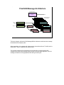
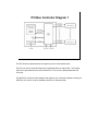
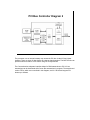
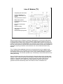
Module Introduction Purpose • This training module covers 68K/ColdFire General Connectivity Peripherals Objectives • Describe the features of the I2S module. • Describe the features and architecture of the FlexCAN communication controller. • Describe the features of the PCI Controller. • Describe the features and functionality of the I2C module. • Describe the features of the UART and PSC modules. • Describe the features of the General purpose digital I/O pins (GPIO) • Describe the features of the Serial Peripheral Interfaces (QSPI & DSPI) Content • 20 pages • 3 questions Learning Time • 30 minutes This module introduces you to the Coldfire 68K General Connectivity Peripherals. In this module, we will step through the I2S module, the FlexCAN communication controller, the PCI Controller, the I2C module, the UART, and PSC modules, GPIO, and the Serial Peripheral Interfaces. Inter-IC Sound (I2S) • Philips IIS and Sony EIAJ protocol capable modes with either 32, 36, or 40 bits per word clock • The frequency of the clock and data signals is programmable, as is the inversion of the bit clock or word clock • Transmitter source programmable • The SCLK and LRCK signals can be inputs to the interface or they can be generated internally There are 4 serial audio interfaces capable of handling Philips IIS or Sony EIAJ protocol with either 32, 36, or 40 bits per word clock. Interface 1 is a receive/transmit interface, interface 2 is a transmit only, interfaces 3 and 4 are receive only. Every audio interface has a 32-bit configuration register where the frequency of the clock and data signals is programmable, as is the inversion of the bit clock and word clock. The two IIS/EIAJ transmitters operate independently and have the capability to transmit data from one of several programmable sources. • One of three processor data out registers, • One of three IIS receivers, • Digital audio (EBU) receiver, or • Digital zero. SCLK and LRCK signals can be external inputs or generated internally. FlexCAN (FlexCAN) FEATURES • Full implementation of the CAN protocol specification - Version 2.0 • Programmable Bit Rate up to 1Mbit/sec • Rx or Tx, all support Standard and Extended Messages. • Listen-only Mode • Programmable transmit-first scheme: Lowest ID or lowest buffer number. • Time Stamp, based on 16-bit freerunning timer. Another module in the ColdFire Family of devices is the FlexCAN module. The FlexCAN module is a communication controller that fully implements the Controller Area Network or CAN protocol specification– Version 2.0. It is based on and includes all existing Motorola TOUCAN module features. It is also a high speed, short distance, priority based protocol which has a programmable bit rate up to 1 Mbit/sec. It can communicate using a variety of mediums, such as fiber optic cable or unshielded twisted pair cable. Although it can be used in other capacities, the CAN protocol was primarily designed to be used as a vehicle serial data bus, meeting the specific requirements of this field: real-time processing, reliable operation in the EMI environment of a vehicle, cost-effectiveness, and required bandwidth. It has Version 2.0 Flexible Message Buffers (up to 16 message buffers) of 0-8 bytes Data Length, each configurable as Rx or Tx. All of them support standard and extended messages. It also includes either 512 byte or 256 byte of RAM, which is used for the message buffers. In listen-only mode, the FlexCAN module is able to receive messages without giving an acknowledgment. Whenever the module enters this mode the status of the Error Counters is frozen and the FlexCAN module operates in a CAN error passive mode. Since the module does not influence the CAN bus in this mode the host device is capable of functioning like a monitor or for automatic bit-rate detection. Message-transmission priority logic provides a programmable "transmit first" mechanism based on the lowest value (highest priority) address identifier or the lowest physical buffer number. The value of the free-running 16-bit timer is sampled at the beginning of the identifier field on the CAN bus. For a message being received, the time stamp will be stored in the time stamp entry of the receive message buffer at the time the message is written into that buffer. For a message being transmitted, the time stamp entry will be written into the transmit message buffer once the transmission has completed successfully. FlexCAN (FlexCAN) FEATURES MORE FEATURES • Full implementation of the CAN protocol specification - Version 2.0 • Global network time, synchronized by a specific message. • Programmable Bit Rate up to 1Mbit/sec • Maskable interrupts • Rx or Tx, all support Standard and Extended Messages. • Multimaster concept • Open network architecture • Listen-only Mode • High immunity to EMI • Programmable transmit-first scheme: Lowest ID or lowest buffer number. • Short latency time for high-priority messages • Time Stamp, based on 16-bit freerunning timer. • Low power sleep mode, with programmable wake up on bus activity Here are more features offered by the FlexCAN module. In Timer synchronize mode, the mechanism that resets the free-running timer each time a message is received in Message Buffer 0 is enabled. This feature provides the means to synchronize multiple FlexCAN stations with a special “SYNC” message. For example, with a global network time. The module can generate up to 19 interrupt sources (16 interrupts due to message buffers and 3 interrupts due to Bus-off, Error and Wake-up). Each one of the message buffers can be an interrupt source, if its corresponding bit is set in the Interrupt Mask Register. The FlexCAN module also supports open network architecture, which means that it permits all users of the basic network to interconnect to specific basic network functions and interfaces on an unbundled, equal-access basis. This module also features a multimaster system that allows any node to initiate a CAN message to all system nodes as soon as the bus is idle. In this type of network, each node filters unwanted messages. A differential bus also provides excellent noise immunity due to the inherent noise cancellation characteristics achieved by using a shielded cable with a twisted wire pair. Since the 11- or 29-bit message identifier associated with each CAN message also determines the priority of a message with respect of the bus access, a very efficient means for transmitting high priority messages with very short latency time is provided even at times of high bus load. Lastly, the module also has the ability to enter the low-power stop mode for power saving purposes. It can exit low-power stop mode either manually or via the self-wake mechanism. FlexCAN Message Architecture All registers 16-bits CONTROL INT 16 Transmit/Receive Message Buffers Tx SERIAL BUFFERS BUFFERS 0-13 BUFFER 14 Rx *transparent to user GLOBAL MASK BUFFER 15 DATA 29 bit DATA LENGTH MASK 14 MASK 15 TIME STAMP ID This block diagram outlines the CAN Message Buffer Architecture and shows the message transmission and reception paths. When transmitting, the message with highest priority is transferred from a Tx buffer into the serial buffer. Then, it is shifted out one bit at a time. The received message is first assembled in the serial buffer, and the message ID is compared to the IDs of the message buffers using the Receive Mask Registers. Then, the message is filtered into the appropriate buffer having a matching ID. Question Which of the following is the name of the component of the FlexCAN message architecture that is indicated by the red arrow? Click the correct answer. A) B) C) D) Serial Buffers Flexible Message Buffer Watchdog Control Register Reset Controller All registers 16-bits CONTROL INT 16 Transmit/Receive Message Buffers BUFFERS 0-13 Tx BUFFER 14 Rx GLOBAL MASK BUFFER 15 DATA 29 bit DATA LENGTH MASK 14 MASK 15 Consider this question about the FlexCAN message architecture. Correct! The indicated component is the Serial Buffers. TIME STAMP ID PCI Controller (PCI) • Compatible with PCI 2.2 specification • Interfaces with 33MHz and 66MHz PCI Busses • PCI initiator and target operation • On-chip DMA and CPU have access to PCI Bus • 32-bit PCI Address and Data bus • The MCF547x and MCF548x can be utilized to interface with an additional FEC, IDE, USB Host, WLAN, graphics controller, etc • Support for up to five external masters The peripheral component interface (PCI) bus is a high-performance bus with multiplexed address and data lines. It is especially suitable for high data-rate applications. It can run at clock speeds of 33 or 66 MHz. With a 32 bit bus running at 33 MHz, the throughput approaches a rate of 133 Mbytes/s. And at 66MHz should be able to net 266Mbytes/s. A PCI transfer is started by a master and is directed toward a specific target. The MCF547x PCI module provides both master and target PCI bus interfaces. The internal master, or initiator, interface is accessible by any XL bus master, such as the processor core. Data is transferred through the use of memory and I/O read and write commands. There is also a DMA interface through the communication subsystem that can be accessed by the mulltichannel DMA engine. This is very useful for allowing the MCF547x to provide continuous data to the PCI module since the basic PCI bus transfer mechanism is a burst. The PCI conventional hardware specification defines either a 32-bit or 64-bit bus width. In the instantiation of the ColdFire MCF547x-8x, the module has been implemented with a 32-bit bus. Its high speed and Plug & Play implementation means that the PCI is the dominant board-level bus on modern PCs. This makes the PCI an attractive bus for connecting to numerous other devices such as additional Fast Ethernet Controllers, Integrated Drive Electronics, Universal Serial Bus Hosts, and so on. PCI Bus Controller Diagram 1 This PCI local bus implementation will support up to four add-in board cards. The PCI bus clock to external PCI devices is generated from an external PLL. The internal PCI clock is generated from the CPUs internal PLL. The XL bus is always faster than the PCI clock. The MCF547x- 8x has an internal arbiter that supports up to 5 external masters including the MCF547x- 8x device. It can be disabled to allow for an external arbiter. PCI Bus Controller Diagram 2 The processor core or internal masters may access the PCI bus via the XL Bus initiator interface. There are three 32-byte buffers to enhance data throughput. The MCF547x-8x can provide continuous data to a PCI master using two 32-byte buffers. The Communication subsystem interface allows for DMA transactions to PCI. XL bus transactions can be interleaved while Comm Bus transactions in progress. The transmit and receive FIFOs, which are not outlined in this diagram, are 32 x 36 bits and support PCI bursts up to 8 beats. Inter-IC Module (I2C) Compatibility with I2C bus standard Interface for EEPROMs, LCD controllers, A/D converters, and keypads Two-wire bidirectional serial bus Multiple master operation Programmable for one of 64 clock frequencies Interrupt driven, byte-by-byte transfer Automatic switching Start and stop signal generation and detection Repeated START signal generation Now let’s examine the I2C Module. As shown in the diagram, it is a two-wire, bidirectional serial bus that provides a simple, efficient method of data exchange between devices. It is compatible with the widely used “I squared C” bus standard and is used as an interchip bus interface for devices such as EEPROMs, LCD controllers, A/D converters, and keypads.This two-wire multi-master bus minimizes the interconnection between devices and is suitable for applications requiring occasional communications over a short distance between many devices. The I2C Module allows additional devices to be connected to the bus for expansion and system development. The I2C Module is a true multimaster bus including collision detection and arbitration that prevents data corruption if two or more masters attempt to control the bus simultaneously. The interface operates up to 100 kilobits per second with maximum bus loading and timing. Some of the features include one of 64 serial clock frequencies that can be selected under software control, software selectable acknowledge bit, stop and start signal generation and detection, repeat start signal generation, interrupt on per byte transfer, and bus busy detection. In addition, the I2C Module has calling address recognition and interrupt generation and will automatically switch from master to slave on arbitration loss. Question Which of the following are features of the I2C Module? A. It is a two-wire, bidirectional serial bus. B. It operates up to 50 kilobits per second with maximum bus loading and timing. C. It provides an interface for I2C EEPROMs, LCD controllers, A/D converters, keypads. D. It has calling address recognition and interrupt generation. Consider this question about the I2C module. Correct! I2C’s features include two-wire serial bus, to interface with I2C EEPROMs, LCD controllers, A/D converters, and keypads. It also has calling address recognition and interrupt generation. UART Modules (UART) UART Internal Channel Control Logic Serial Communications Channel /CTS /RTS RxD TxD SIM Module Interrupt Controller • • • • Internal Bus Clock or External Clock (DTIN) 5-8 data bits plus parity Odd, even, no parity 9/16 to 2 stop bits Four programmable channel modes: – – – – • Programmable Clock Generation Full duplex Asynchronous/Synchronous receiver/transmitter channels Each can be clocked by the internal bus clock or an external clock. Independently programmable receiver and transmitter clock sources Programmable data format: – – – • Interrupt Control Logic Normal (full-duplex) Automatic echo Local loop-back Remote loop-back mode The number of UARTs and supported features can vary from device to device. Please refer to the product brief or user’s manual for the specific device for more information. The next module we’ll examine is the universal asynchronous receiver/transmitter (UART). The UART module provides for full duplex asynchronous/synchronous receive and transmit communication. Each UART can be clocked by the Internal Bus Clock. UARTs can also be clocked by an external clock connected to the DTIN pin. In addition the receiver and transmitter can be clocked independently so that they use two different clock sources. The UART supports several options for the data format. The number of data bits can range between 5 and 8. Parity modes are odd, even, or no parity. The number of stop bits can range between 9/16 and 2 There are four programmable channel modes. Normal mode is the standard full-duplex operating mode. The three other modes are special cases that are used primarily for testing. Automatic echo mode takes the received data and retransmits it on a bit-by-bit basis. The local CPU-to-receiver communication continues normally but the CPU-to-transmitter link is disabled. Local loopback mode ties the receive and transmit pins together internally. This mode is useful for testing the operation of the local UART module channel by sending data to the transmitter and checking data assembled by the receiver. Both transmitter and CPU-to-receiver communications continue normally in this mode. Remote loopback mode automatically retransmits received data just as automatic echo mode does, except that both the receiver and transmitter are disabled from the CPU. This mode is useful for testing remote channel receiver and transmitter operation. The number of UARTs and supported features can vary from device to device. Please refer to the product brief or user’s manual for the specific device for more information. Let’s take a closer look at normal mode consisting of the receiver and transmitter. UART Receiver Features (UART) • 4-stage FIFO receive buffer • Frame, parity, and overrun error detections • Detection of a break originating in the middle of a character • Automatic wakeup for multidrop applications • Start/end break interrupt status The receiver has a 4-character FIFO buffer. Interrupts can be generated when the first character is received or when the FIFO is full. Reading the FIFO will pop the stack, allowing space for one more character to be received. A status register contains information on error conditions, such as framing error, parity error, and overrun error. A bit for detecting a break character is also contained in this register. The receiver operation can be either polled or interrupt driven. You can program the receiver to operate in a wakeup mode for multidrop or multiprocessor applications. This mode of operation connects a master station to several slave stations. The slave stations’ UART receivers are disabled; however they continuously monitor the data stream sent out by the master station. When the master sends an address character, the slave receivers notify their respective CPUs by causing an interrupt. Each slave station CPU then compares the received address to its station address and enables its receiver if it wants to receive the subsequent data stream. Next, we’ll check out the UART transmitter. UART Transmitter Features (UART) • Double-buffered operation • Programmable character length from 5 to 8 bits • Parity generation: odd, even, no parity, or force parity • Break generation • Automatic negation of request-to-send upon completion of message transmission • Baud Rate = Fsys / ( 32 * (UBG1 \\ UBG2) ) The UART transmitter is double buffered and can be programmed to transmit data formatted from 5 to 8 data bits plus parity. Parity can be either odd, even, none or forced. Forced parity simply means that the parity bit is forced either to a 1 or a 0, regardless of the actual parity. If selected, parity is automatically calculated by the UART. The UART has break character generation capability and can be programmed to send up to 2 stop bits. Full handshaking can be implemented with the request to send (RTS) and clear to send (CTS) pins. You can program the transmitter to automatically negate the request to send output on completion of a message transmission. If clear to send is enabled, the CTS input must be asserted for the character to be transmitted. All standard baud rates up to 115K and higher can be achieved by using the internal system clock. When using this clock, the formula to calculate the baud rate is: divide the system clock frequency by 32, and then divide the answer by the concatenation of the decimal value in the UBG1 and UBG2 registers. For example, to generate a baud rate of 19.2K with a 50 MHz system clock, you would program the UBG1 register to 0 and UBG2 register with decimal 81 or 51 hex. Question Which of the following are features of the UART module? A. A status register contains information on error conditions, such as framing error, parity error, and overrun error. B. Each UART is clocked by the internal bus clock and cannot be clocked externally. C. Two IIS/EIAJ transmitters operate independently and have the capability to transmit data from one of several sources. D. It has break character generation capability and can be programmed to send up to 2 stop bits. Take a moment to answer this question about the UART module. Correct! A status register contains information on error conditions, such as framing error, parity error, and overrun error. And, the UART module has break character generation capability and can be programmed to send up to 2 stop bits. Programmable Serial Controllers • Full duplex receiver and transmitter in all modes • 7 operation modes – UART – 3 soft modem modes (modem8, modem16, and AC97) – 3 IrDA modes (SIR, MIR, and FIR) • Two 512 byte FIFOs • All can be controlled by DMA The PSC module is a feature rich serial controller with support for standard serial protocols. There are seven different modes supported: UART, three modem modes, and three IrDA modes. This module is featured on the MCF547x and MCF548x device families. Those devices implement the PSC with two FIFOs for each PSC channel; one for the receiver and one for the transmitter. Each FIFO is 512 bytes in length and may be serviced by the DMA or the CPU. QSPI Module (QSPI) Serial interface to control external peripherals or transfer data Programmable bit rates, clock polarity and phase End-of-transmission interrupt flag, master-master mode fault flag Programmable queue : Up to 16 pre-programmed transfers Wraparound transfer mode with no CPU overhead Programmable transfer length, transfer delay, queue pointer Four programmable peripheral chip-selects One dedicated chip select output Three chip selects multiplexed with other pin functions general purpose I/O port pins can be used as chip selects Another important component of ColdFire is the Queued Serial Peripheral Interface (QSPI) module. This module provides a serial peripheral interface with queued transfer capability. It allows users to queue up to 16 transfers at once, eliminating CPU intervention between transfers. The RAM within the QSPI is indirectly accessible using address and data registers. Functionality is very similar, but not identical, to the QSPI portion of the Queued Serial Module (QSM) implemented in the long-time popular Motorola MC68332. It includes a serial interface to control external peripherals or transfer data. It also has programmable bit rates that clock polarity and phase. In addition, it includes a programmable end-of-transmission interrupt flag. The QSPI has a programmable queue that includes up to 16 pre-programmed transfers. It also has a wraparound transfer mode with no CPU overhead. The module has a programmable transfer length, a transfer delay, and a queue pointer. The module has four programmable peripheral chip-selects including one dedicated chip select output and three chip selects multiplexed with other pin functions. More than one chip select may be active at once, and more than one device can be connected to each chip select, allowing up to 15 devices to be connected to the module. DMA Serial Peripheral Interface • Full-duplex, three-wire synchronous transfers • Master and Slave Mode • Four peripheral chip selects, expandable to 15 with external demultiplexer • Deglitching support for up to 7 peripheral chip selects with external demultiplexer • DMA Support • Buffered transmit and receive operation using the TX FIFO and RX FIFO with depth of 4 entries • Programmable transfer attributes on a per-frame basis The DSPI provides similar functionality to the QSPI module found on other ColdFire products. It uses a three-wire serial bus for full-duplex traffic. The major difference between the DSPI functionality and the QSPI functionality is that the DSPI can support both master and slave modes, whereas the QSPI only supports master mode operation. The DSPI provides up to four peripheral chip selects for selecting external devices. In addition, some of the chip selects have special functions. When in slave mode, DSPI_CS0 is used as the slave select signal. This input is asserted by the DSPI master to let the ColdFire know when it is being accessed. In master mode, DSPI_CS5 can be used as a peripheral chip select strobe used with an external demultiplexer to generate 7 peripheral chip selects from the remaining DSPI chip select signals. The DSPI has the ability to trigger DMA transfers in order to drain or fill the receive and transmit FIFOs. The size of the DSPI FIFOs are implementation dependent. Current ColdFire parts support four entries in each FIFO. Refer to the reference manual for the particular device to verify the FIFO depth implemented. The DSPI also supports programmable transfer attributes, such as clock polarity, transfer size, endianness, and timing. These attributes are programmable on a transfer by transfer basis. GPIO • General purpose I/O support for all ports — Registers for storing output pin data — Registers for controlling pin data direction — Registers for reading current pin state — Registers for setting and clearing output pin data registers — Programmable drive strength control • • • • Grouped by port/pin function (523x, 5270/1, 5274/5) Per pin basis (5208, 5211/2/3, 522x, 532x, 537x) Programmable slew rate control (5211/2/3, 522x) SDRAM technology-specific drive capability (5207/8, 532x, 537x, 547x, 548x) • NOTE: By default most pins default to general purpose input functionality. When not used for other functions, all of the pins may be used as general purpose digital I/O pins. In some cases, the pin function is set by the operating mode, and the alternate pin functions are not supported. The GPIO register architecture is grouped by port or pin function depending on the specific device. Every GPIO can individually be controlled on a pin per pin basis. On some devices, the slew rate can be controlled to configure the pin for fast slew rate or for slow slew rate, which adds a delay that is approximately 10 times slower. Lastly, on some devices SDRAM technology-specific drive capability has been added to control the output mode selects of the SDRAM pins. Out of reset, most pins will default to their GPIO functionality, so the associated peripheral functionality will have to be enabled. The pin assignment registers allow the user to select between digital I/O or another pin function after reset. All of the pins associated with the external bus interface may be used for several different functions. Their primary function is to provide an external memory interface to access off-chip resources. Module Summary I2S module FlexCAN communication controller PCI controller I2C module UART and PSC modules Serial Peripheral Interface (QSPI & DSPI) General purpose digital I/O pins (GPIO) In this module you learned about the I2S module, the FlexCAN communication controller, the PCI Controller, the I2C module, the UART, and PSC modules, the Serial Peripheral Interface, and the General purpose digital I/O module.