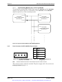
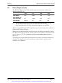
1
Artisan Technology Group is your source for quality
new and certified-used/pre-owned equipment
• FAST SHIPPING AND
DELIVERY
• TENS OF THOUSANDS OF
IN-STOCK ITEMS
• EQUIPMENT DEMOS
• HUNDREDS OF
MANUFACTURERS
SUPPORTED
• LEASING/MONTHLY
RENTALS
• ITAR CERTIFIED
SECURE ASSET SOLUTIONS
SERVICE CENTER REPAIRS
Experienced engineers and technicians on staff
at our full-service, in-house repair center
WE BUY USED EQUIPMENT
Sell your excess, underutilized, and idle used equipment
We also offer credit for buy-backs and trade-ins
www.artisantg.com/WeBuyEquipment
InstraView REMOTE INSPECTION
LOOKING FOR MORE INFORMATION?
Visit us on the web at www.artisantg.com for more
information on price quotations, drivers, technical
specifications, manuals, and documentation
SM
Remotely inspect equipment before purchasing with
our interactive website at www.instraview.com
Contact us: (888) 88-SOURCE | [email protected] | www.artisantg.com
EXC-4000PCI Family
Test and Simulation Carrier Boards
for PCI Systems
EXC-4000PCI
EXC-4000cPCI
EXC-4000cPCI6U
EXC-4000PCIe
User’s Manual
311 Meacham Ave ♦ Elmont
e-mail: [email protected]
♦
NY 11003
♦
tel. (516) 327-0000 ♦ fax (516) 327-4645
website: www.mil-1553.com
Artisan Technology Group - Quality Instrumentation ... Guaranteed | (888) 88-SOURCE | www.artisantg.com
Artisan Technology Group - Quality Instrumentation ... Guaranteed | (888) 88-SOURCE | www.artisantg.com
Table of Contents
Table of Contents
1 Introduction
1.1
1.1.1
1.1.2
1.1
1.1.1
1.1.2
1.1
Overview . . . . . . . . . . . . . . . . . . . . . . . . . . . . . . . . . . . . . . . . . . . . . . . . . . . . . . . . . . . . . .1-1
EXC-4000PCI[e] Board Features . . . . . . . . . . . . . . . . . . . . . . . . . . . . . . . . . . . . . . . . . . . . . . . . . . 1-2
EXC-4000PCI[e] Block Diagram . . . . . . . . . . . . . . . . . . . . . . . . . . . . . . . . . . . . . . . . . . . . . . . . . . . 1-3
Installation . . . . . . . . . . . . . . . . . . . . . . . . . . . . . . . . . . . . . . . . . . . . . . . . . . . . . . . . . . . . .1-4
Installing the Board . . . . . . . . . . . . . . . . . . . . . . . . . . . . . . . . . . . . . . . . . . . . . . . . . . . . . . . . . . . . . 1-4
Adding Excalibur Software Tools. . . . . . . . . . . . . . . . . . . . . . . . . . . . . . . . . . . . . . . . . . . . . . . . . . . 1-4
Technical Support. . . . . . . . . . . . . . . . . . . . . . . . . . . . . . . . . . . . . . . . . . . . . . . . . . . . . . .1-4
2 PCI Architecture
2.1
Memory Structure . . . . . . . . . . . . . . . . . . . . . . . . . . . . . . . . . . . . . . . . . . . . . . . . . . . . . . .2-2
2.2
PCI Configuration Space Header. . . . . . . . . . . . . . . . . . . . . . . . . . . . . . . . . . . . . . . . . . .2-3
2.3
PCI Configuration Registers . . . . . . . . . . . . . . . . . . . . . . . . . . . . . . . . . . . . . . . . . . . . . .2-5
2.3.1
2.3.2
2.3.3
2.3.4
2.3.5
2.3.6
2.3.7
2.3.8
2.3.9
2.3.10
2.3.11
2.3.12
2.3.13
2.3.14
2.3.15
2.3.16
2.3.17
2.3.18
2.3.19
2.3.20
2.4
2.4.1
2.4.2
2.4.3
2.4.4
2.4.5
2.4.6
2.4.7
2.4.8
Vendor Identification Register (VID) . . . . . . . . . . . . . . . . . . . . . . . . . . . . . . . . . . . . . . . . . . . . . . . . 2-5
Device Identification Register (DID). . . . . . . . . . . . . . . . . . . . . . . . . . . . . . . . . . . . . . . . . . . . . . . . . 2-5
PCI Command Register (PCICMD) . . . . . . . . . . . . . . . . . . . . . . . . . . . . . . . . . . . . . . . . . . . . . . . . . 2-5
PCI Status Register (PCISTS). . . . . . . . . . . . . . . . . . . . . . . . . . . . . . . . . . . . . . . . . . . . . . . . . . . . . 2-6
Revision Identification Register (RID) . . . . . . . . . . . . . . . . . . . . . . . . . . . . . . . . . . . . . . . . . . . . . . . 2-7
Class Code Register (CLCD). . . . . . . . . . . . . . . . . . . . . . . . . . . . . . . . . . . . . . . . . . . . . . . . . . . . . . 2-7
Cache Line Register Size Register (CALN). . . . . . . . . . . . . . . . . . . . . . . . . . . . . . . . . . . . . . . . . . . 2-8
Latency Timer Register (LAT) . . . . . . . . . . . . . . . . . . . . . . . . . . . . . . . . . . . . . . . . . . . . . . . . . . . . . 2-8
Header Type Register (HDR) . . . . . . . . . . . . . . . . . . . . . . . . . . . . . . . . . . . . . . . . . . . . . . . . . . . . . 2-8
Built-In Self-Test Register (BIST) . . . . . . . . . . . . . . . . . . . . . . . . . . . . . . . . . . . . . . . . . . . . . . . . . 2-8
Base Address Registers (BADR). . . . . . . . . . . . . . . . . . . . . . . . . . . . . . . . . . . . . . . . . . . . . . . . . . 2-9
Cardbus CIS Pointer . . . . . . . . . . . . . . . . . . . . . . . . . . . . . . . . . . . . . . . . . . . . . . . . . . . . . . . . . . 2-10
Subsystem ID . . . . . . . . . . . . . . . . . . . . . . . . . . . . . . . . . . . . . . . . . . . . . . . . . . . . . . . . . . . . . . . 2-10
Subvendor ID. . . . . . . . . . . . . . . . . . . . . . . . . . . . . . . . . . . . . . . . . . . . . . . . . . . . . . . . . . . . . . . . 2-10
Expansion ROM Base Address Register (XROM). . . . . . . . . . . . . . . . . . . . . . . . . . . . . . . . . . . . 2-10
PCI Capabilities Pointer. . . . . . . . . . . . . . . . . . . . . . . . . . . . . . . . . . . . . . . . . . . . . . . . . . . . . . . . 2-10
Interrupt Line Register (INTLN) . . . . . . . . . . . . . . . . . . . . . . . . . . . . . . . . . . . . . . . . . . . . . . . . . . 2-11
Interrupt Pin Register (INTPIN) . . . . . . . . . . . . . . . . . . . . . . . . . . . . . . . . . . . . . . . . . . . . . . . . . . 2-11
Minimum Grant Register (MINGNT) . . . . . . . . . . . . . . . . . . . . . . . . . . . . . . . . . . . . . . . . . . . . . . 2-11
Maximum Latency Register (MAXLAT) . . . . . . . . . . . . . . . . . . . . . . . . . . . . . . . . . . . . . . . . . . . . 2-11
DMA Registers for PCI Express. . . . . . . . . . . . . . . . . . . . . . . . . . . . . . . . . . . . . . . . . . .2-12
DMA0 Address of Contiguous Host Memory (Low and High) . . . . . . . . . . . . . . . . . . . . . . . . . . . .
DMA0 Data Transfer Size . . . . . . . . . . . . . . . . . . . . . . . . . . . . . . . . . . . . . . . . . . . . . . . . . . . . . . .
DMA0 Control Register . . . . . . . . . . . . . . . . . . . . . . . . . . . . . . . . . . . . . . . . . . . . . . . . . . . . . . . . .
DMA1 Address of Contiguous Host Memory . . . . . . . . . . . . . . . . . . . . . . . . . . . . . . . . . . . . . . . . .
DMA1 Data Transfer Size . . . . . . . . . . . . . . . . . . . . . . . . . . . . . . . . . . . . . . . . . . . . . . . . . . . . . . .
DMA1 Control Register . . . . . . . . . . . . . . . . . . . . . . . . . . . . . . . . . . . . . . . . . . . . . . . . . . . . . . . . .
DMA Interrupt Status Register. . . . . . . . . . . . . . . . . . . . . . . . . . . . . . . . . . . . . . . . . . . . . . . . . . . .
Base Address for DMA0 and DMA1 Transfers . . . . . . . . . . . . . . . . . . . . . . . . . . . . . . . . . . . . . . .
2-12
2-13
2-13
2-13
2-14
2-14
2-15
2-15
2.5
Module Memory Space Map . . . . . . . . . . . . . . . . . . . . . . . . . . . . . . . . . . . . . . . . . . . . . .2-15
2.6
EXC-4000PCI[e] Global Registers Map . . . . . . . . . . . . . . . . . . . . . . . . . . . . . . . . . . . . .2-16
2.6.1
2.6.2
2.6.3
2.6.4
2.6.5
2.6.6
2.6.7
Board Identification Register . . . . . . . . . . . . . . . . . . . . . . . . . . . . . . . . . . . . . . . . . . . . . . . . . . . . .
Software Reset Register . . . . . . . . . . . . . . . . . . . . . . . . . . . . . . . . . . . . . . . . . . . . . . . . . . . . . . . .
Interrupt Status Register . . . . . . . . . . . . . . . . . . . . . . . . . . . . . . . . . . . . . . . . . . . . . . . . . . . . . . . .
Interrupt Reset Register . . . . . . . . . . . . . . . . . . . . . . . . . . . . . . . . . . . . . . . . . . . . . . . . . . . . . . . .
Module Info Registers . . . . . . . . . . . . . . . . . . . . . . . . . . . . . . . . . . . . . . . . . . . . . . . . . . . . . . . . . .
Time Tag Clock Select Register . . . . . . . . . . . . . . . . . . . . . . . . . . . . . . . . . . . . . . . . . . . . . . . . . .
Byte Swapping. . . . . . . . . . . . . . . . . . . . . . . . . . . . . . . . . . . . . . . . . . . . . . . . . . . . . . . . . . . . . . . .
EXC-4000PCI Family Carrier Boards: User’s Manual
Artisan Technology Group - Quality Instrumentation ... Guaranteed | (888) 88-SOURCE | www.artisantg.com
2-17
2-17
2-18
2-18
2-19
2-19
2-19
page i
Table of Contents
2.6.8
2.7
2.7.1
2.7.2
2.7.3
2.7.4
2.7.5
2.7.6
2.7.7
2.7.8
2.7.9
2.8
2.8.1
2.8.2
2.8.3
2.8.4
FPGA Revision Register . . . . . . . . . . . . . . . . . . . . . . . . . . . . . . . . . . . . . . . . . . . . . . . . . . . . . . . . 2-20
IRIG B Global Registers . . . . . . . . . . . . . . . . . . . . . . . . . . . . . . . . . . . . . . . . . . . . . . . . .2-20
Sync IRIG B Register . . . . . . . . . . . . . . . . . . . . . . . . . . . . . . . . . . . . . . . . . . . . . . . . . . . . . . . . . .
IRIG B Time SBS High Register . . . . . . . . . . . . . . . . . . . . . . . . . . . . . . . . . . . . . . . . . . . . . . . . . .
IRIG B Time SBS Low Register. . . . . . . . . . . . . . . . . . . . . . . . . . . . . . . . . . . . . . . . . . . . . . . . . . .
IRIG B Time Days Register . . . . . . . . . . . . . . . . . . . . . . . . . . . . . . . . . . . . . . . . . . . . . . . . . . . . . .
IRIG B Time Hours Register . . . . . . . . . . . . . . . . . . . . . . . . . . . . . . . . . . . . . . . . . . . . . . . . . . . . .
IRIG B Time Minutes Register . . . . . . . . . . . . . . . . . . . . . . . . . . . . . . . . . . . . . . . . . . . . . . . . . . . .
IRIG B Time Seconds Register . . . . . . . . . . . . . . . . . . . . . . . . . . . . . . . . . . . . . . . . . . . . . . . . . . .
Control Functions Registers . . . . . . . . . . . . . . . . . . . . . . . . . . . . . . . . . . . . . . . . . . . . . . . . . . . . .
FPGA Revision Register . . . . . . . . . . . . . . . . . . . . . . . . . . . . . . . . . . . . . . . . . . . . . . . . . . . . . . . .
2-21
2-21
2-21
2-21
2-22
2-22
2-22
2-22
2-22
Global Timer Registers. . . . . . . . . . . . . . . . . . . . . . . . . . . . . . . . . . . . . . . . . . . . . . . . . .2-23
Timer Prescale Register . . . . . . . . . . . . . . . . . . . . . . . . . . . . . . . . . . . . . . . . . . . . . . . . . . . . . . . .
Timer Preload Register . . . . . . . . . . . . . . . . . . . . . . . . . . . . . . . . . . . . . . . . . . . . . . . . . . . . . . . . .
Timer Control Register. . . . . . . . . . . . . . . . . . . . . . . . . . . . . . . . . . . . . . . . . . . . . . . . . . . . . . . . . .
General Purpose Timer Register . . . . . . . . . . . . . . . . . . . . . . . . . . . . . . . . . . . . . . . . . . . . . . . . . .
2-23
2-23
2-23
2-24
3 Mechanical and Electrical Specifications
3.1
3.1.1
3.1.2
3.1.3
3.1.4
Board Layout . . . . . . . . . . . . . . . . . . . . . . . . . . . . . . . . . . . . . . . . . . . . . . . . . . . . . . . . . . .3-2
EXC-4000PCI . . . . . . . . . . . . . . . . . . . . . . . . . . . . . . . . . . . . . . . . . . . . . . . . . . . . . . . . . . . . . . . . .
EXC-4000PCIe . . . . . . . . . . . . . . . . . . . . . . . . . . . . . . . . . . . . . . . . . . . . . . . . . . . . . . . . . . . . . . . .
EXC-4000cPCI . . . . . . . . . . . . . . . . . . . . . . . . . . . . . . . . . . . . . . . . . . . . . . . . . . . . . . . . . . . . . . . .
EXC-4000cPCI6U . . . . . . . . . . . . . . . . . . . . . . . . . . . . . . . . . . . . . . . . . . . . . . . . . . . . . . . . . . . . . .
3-2
3-2
3-3
3-4
3.2
Led Indicators . . . . . . . . . . . . . . . . . . . . . . . . . . . . . . . . . . . . . . . . . . . . . . . . . . . . . . . . . .3-5
3.3
DIP Switches . . . . . . . . . . . . . . . . . . . . . . . . . . . . . . . . . . . . . . . . . . . . . . . . . . . . . . . . . . .3-5
3.3.1
3.4
3.4.1
3.4.2
3.4.3
3.4.4
3.4.5
3.5
Selected ID DIP Switch [SW1]. . . . . . . . . . . . . . . . . . . . . . . . . . . . . . . . . . . . . . . . . . . . . . . . . . . . . 3-5
Connectors . . . . . . . . . . . . . . . . . . . . . . . . . . . . . . . . . . . . . . . . . . . . . . . . . . . . . . . . . . . .3-6
List of Connectors Per Carrier Board. . . . . . . . . . . . . . . . . . . . . . . . . . . . . . . . . . . . . . . . . . . . . . . . 3-6
Communications I/O Connectors. . . . . . . . . . . . . . . . . . . . . . . . . . . . . . . . . . . . . . . . . . . . . . . . . . . 3-9
PCI, PCI Express and cPCI Bus Connectors . . . . . . . . . . . . . . . . . . . . . . . . . . . . . . . . . . . . . . . . 3-25
External Signals Connector [J2] . . . . . . . . . . . . . . . . . . . . . . . . . . . . . . . . . . . . . . . . . . . . . . . . . . 3-28
Power Connector for EXC-4000PCIe Express Cards . . . . . . . . . . . . . . . . . . . . . . . . . . . . . . . . . . 3-30
Power Requirements . . . . . . . . . . . . . . . . . . . . . . . . . . . . . . . . . . . . . . . . . . . . . . . . . . .3-31
4 Ordering Information
page ii
Excalibur Systems
Artisan Technology Group - Quality Instrumentation ... Guaranteed | (888) 88-SOURCE | www.artisantg.com
Table of Contents
Figures
Figure 1-1
Figure 2-1
Figure 2-2
Figure 2-3
Figure 2-4
Figure 3-1
Figure 3-2
Figure 3-3
Figure 3-4
Figure 3-5
Figure 3-6
Figure 3-7
Figure 3-8
Figure 3-9
Figure 3-10
Figure 3-11
Figure 3-12
Figure 3-13
Figure 3-14
Figure 3-15
Figure 3-16
Figure 3-17
Figure 3-18
Figure 3-19
Figure 3-20
Figure 3-21
Figure 3-22
EXC-4000PCI[e] Block Diagram . . . . . . . . . . . . . . . . . . . . . . . . . . . . . . . . . . . . . . . . . . . . . 1-3
PCI Configuration Space Header. . . . . . . . . . . . . . . . . . . . . . . . . . . . . . . . . . . . . . . . . . . . . 2-3
PCI Express Configuration Space Header. . . . . . . . . . . . . . . . . . . . . . . . . . . . . . . . . . . . . . 2-4
Module Memory Space Map . . . . . . . . . . . . . . . . . . . . . . . . . . . . . . . . . . . . . . . . . . . . . . . 2-15
EXC-4000PCI[e] Global and IRIG B Registers Map . . . . . . . . . . . . . . . . . . . . . . . . . . . . . 2-16
EXC-4000PCI Board Layout . . . . . . . . . . . . . . . . . . . . . . . . . . . . . . . . . . . . . . . . . . . . . . . . 3-2
EXC-4000PCIe Board Layout . . . . . . . . . . . . . . . . . . . . . . . . . . . . . . . . . . . . . . . . . . . . . . . 3-2
EXC-4000cPCI Board Layout . . . . . . . . . . . . . . . . . . . . . . . . . . . . . . . . . . . . . . . . . . . . . . . 3-3
EXC-4000cPCI6U Board Layout . . . . . . . . . . . . . . . . . . . . . . . . . . . . . . . . . . . . . . . . . . . . . 3-4
DIP Switch SW1 with All Switches Set to ON (Select ID#0) . . . . . . . . . . . . . . . . . . . . . . . . 3-5
96-Pin Female I/O Connector [J1] and Mating Cable Connector – Front View . . . . . . . . . . 3-9
M4K1553Px Module Twinax Connector – Front View . . . . . . . . . . . . . . . . . . . . . . . . . . . . 3-11
M4K429RTx Module Adapter Cable Connector – HDB 26-Pin Female – Front View . . . . 3-13
M4KDiscrete Module Adapter Cable Connector – DB 25-Pin Female – Front View . . . . . 3-14
M4KSerial Module Adapter Cable Connector – DB 25-Pin Male – Front View . . . . . . . . . 3-16
M4KCAN Module Adapter Cable Connector – HDB 26-Pin Male – Front View . . . . . . . . . 3-18
M4K708 Module Twinax Connector – Front View . . . . . . . . . . . . . . . . . . . . . . . . . . . . . . . 3-19
M4KMMSI Module Adapter Cable Connector – HDB 26-Pin Female – Front View . . . . . . 3-21
M4KH009 Module Twinax Connector – Front View . . . . . . . . . . . . . . . . . . . . . . . . . . . . . . 3-22
Rear I/O Connector for 32-Bit cPCI Systems – Front View . . . . . . . . . . . . . . . . . . . . . . . . 3-23
Rear I/O Connector for cPCI6U Systems – Front View . . . . . . . . . . . . . . . . . . . . . . . . . . . 3-24
P1 Bus Connector – Front View. . . . . . . . . . . . . . . . . . . . . . . . . . . . . . . . . . . . . . . . . . . . . 3-27
8-Pin Male Connector [J2] – Front View . . . . . . . . . . . . . . . . . . . . . . . . . . . . . . . . . . . . . . 3-28
Synchronization of a Single EXC-4000PCI[e] board to an External System . . . . . . . . . . . 3-29
Synchronization of an External System to a Single EXC-4000PCI[e] Board . . . . . . . . . . . 3-29
Synchronization Between EXC-4000PCI[e] Boards. . . . . . . . . . . . . . . . . . . . . . . . . . . . . . 3-30
4-Pin Male EXC-4000PCIe Power Connector – Front View . . . . . . . . . . . . . . . . . . . . . . . 3-30
Table 2-1
Table 2-2
Table 2-3
Table 2-4
Table 2-5
Table 2-6
Table 2-7
Table 2-8
Table 2-9
Table 2-10
Table 2-11
Table 2-12
Table 2-13
Table 2-14
Table 2-15
Table 2-16
Table 2-17
Table 2-18
Table 2-19
Table 3-1
Table 3-2
Table 3-3
Table 3-4
Table 3-5
Table 3-6
Table 3-7
PCI Command Register . . . . . . . . . . . . . . . . . . . . . . . . . . . . . . . . . . . . . . . . . . . . . . . . . . . . 2-5
PCI Status Register for PCI Boards . . . . . . . . . . . . . . . . . . . . . . . . . . . . . . . . . . . . . . . . . . . 2-6
PCI Status Register for PCIe Boards . . . . . . . . . . . . . . . . . . . . . . . . . . . . . . . . . . . . . . . . . . 2-7
Base Address Registers Definition for PCI Board. . . . . . . . . . . . . . . . . . . . . . . . . . . . . . . . . 2-9
Base Address Registers Definition for PCIe Board. . . . . . . . . . . . . . . . . . . . . . . . . . . . . . . . 2-9
Base Address Register for PCI Board. . . . . . . . . . . . . . . . . . . . . . . . . . . . . . . . . . . . . . . . . . 2-9
Base Address Register for PCIe Board. . . . . . . . . . . . . . . . . . . . . . . . . . . . . . . . . . . . . . . . 2-10
DMA0 Control Register . . . . . . . . . . . . . . . . . . . . . . . . . . . . . . . . . . . . . . . . . . . . . . . . . . . . 2-13
DMA1 Control Register . . . . . . . . . . . . . . . . . . . . . . . . . . . . . . . . . . . . . . . . . . . . . . . . . . . . 2-14
Board Identification Register . . . . . . . . . . . . . . . . . . . . . . . . . . . . . . . . . . . . . . . . . . . . . . . . 2-17
Software Reset Register . . . . . . . . . . . . . . . . . . . . . . . . . . . . . . . . . . . . . . . . . . . . . . . . . . . 2-17
Interrupt Status Register . . . . . . . . . . . . . . . . . . . . . . . . . . . . . . . . . . . . . . . . . . . . . . . . . . . 2-18
Interrupt Reset Register . . . . . . . . . . . . . . . . . . . . . . . . . . . . . . . . . . . . . . . . . . . . . . . . . . . 2-18
Module Info Registers . . . . . . . . . . . . . . . . . . . . . . . . . . . . . . . . . . . . . . . . . . . . . . . . . . . . . 2-19
Time Tag Clock Select Register . . . . . . . . . . . . . . . . . . . . . . . . . . . . . . . . . . . . . . . . . . . . . 2-19
Byte Swapping Register . . . . . . . . . . . . . . . . . . . . . . . . . . . . . . . . . . . . . . . . . . . . . . . . . . . 2-19
Sync IRIGB Register . . . . . . . . . . . . . . . . . . . . . . . . . . . . . . . . . . . . . . . . . . . . . . . . . . . . . . 2-21
Timer Prescale/General Purpose Timer Resolution . . . . . . . . . . . . . . . . . . . . . . . . . . . . . . 2-23
Timer Control Register . . . . . . . . . . . . . . . . . . . . . . . . . . . . . . . . . . . . . . . . . . . . . . . . . . . . 2-24
Led Indicators . . . . . . . . . . . . . . . . . . . . . . . . . . . . . . . . . . . . . . . . . . . . . . . . . . . . . . . . . . . . 3-5
Dip Switch settings for unique ‘Selected ID’ . . . . . . . . . . . . . . . . . . . . . . . . . . . . . . . . . . . . . 3-5
Selected ID Bits. . . . . . . . . . . . . . . . . . . . . . . . . . . . . . . . . . . . . . . . . . . . . . . . . . . . . . . . . . . 3-5
M4K1553Px Module Terminal Stick and Adapter Cable Pinouts . . . . . . . . . . . . . . . . . . . . 3-10
M4K429RTx Module Terminal Stick and Adapter Cable Pinouts . . . . . . . . . . . . . . . . . . . . 3-12
M4KDiscrete Module Terminal Stick and Adapter Cable Pinouts . . . . . . . . . . . . . . . . . . . . 3-14
M4KSerial Module Terminal Stick and Adapter Cable Pinouts . . . . . . . . . . . . . . . . . . . . . . 3-15
Tables
EXC-4000PCI Family Carrier Boards: User’s Manual
Artisan Technology Group - Quality Instrumentation ... Guaranteed | (888) 88-SOURCE | www.artisantg.com
page iii
Table of Contents
Table 3-8
Table 3-9
Table 3-10
Table 3-11
Table 3-12
Table 3-13
Table 3-14
Table 3-15
Table 3-16
Table 3-17
Table 3-18
Table 3-19
Table 4-1
Table 4-2
page iv
M4KCAN Module Terminal Stick and Adapter Cable Pinouts. . . . . . . . . . . . . . . . . . . . . . . 3-17
M4K708 Module Terminal Stick and Adapter Cable Pinouts . . . . . . . . . . . . . . . . . . . . . . . 3-19
M4KMMSI Module Terminal Stick and Adapter Cable Pinouts. . . . . . . . . . . . . . . . . . . . . . 3-20
M4KH009 Module Terminal Stick and Adapter Cable Pinouts . . . . . . . . . . . . . . . . . . . . . . 3-22
Rear I/O Connector for 32-Bit cPCI Systems Pinouts [P2] . . . . . . . . . . . . . . . . . . . . . . . . . 3-23
Rear I/O Connector for cPCI6U Systems Pinouts [P4] . . . . . . . . . . . . . . . . . . . . . . . . . . . . 3-24
PCI Bus Edge Connector Pinouts . . . . . . . . . . . . . . . . . . . . . . . . . . . . . . . . . . . . . . . . . . . . 3-25
PCI Express Bus Edge Connector Pinouts . . . . . . . . . . . . . . . . . . . . . . . . . . . . . . . . . . . . . 3-26
cPCI Bus Connector Pinouts [P1] . . . . . . . . . . . . . . . . . . . . . . . . . . . . . . . . . . . . . . . . . . . . 3-27
Connector J2 Pinouts . . . . . . . . . . . . . . . . . . . . . . . . . . . . . . . . . . . . . . . . . . . . . . . . . . . . . 3-28
External Signals Description [Connector J2]. . . . . . . . . . . . . . . . . . . . . . . . . . . . . . . . . . . . 3-28
PCIe Power Connector Pin Assignments . . . . . . . . . . . . . . . . . . . . . . . . . . . . . . . . . . . . . . 3-30
Ordering Information . . . . . . . . . . . . . . . . . . . . . . . . . . . . . . . . . . . . . . . . . . . . . . . . . . . . . . . 4-1
M4K Module Codes and Part Numbers . . . . . . . . . . . . . . . . . . . . . . . . . . . . . . . . . . . . . . . . 4-1
Excalibur Systems
Artisan Technology Group - Quality Instrumentation ... Guaranteed | (888) 88-SOURCE | www.artisantg.com
Chapter 1
1
Introduction
Introduction
1.1
Overview . . . . . . . . . . . . . . . . . . . . . . . . . . . . . . . . . . . . . . . . . . . . . . . . . 1-1
1.1.1
1.1.2
1.1
Installation. . . . . . . . . . . . . . . . . . . . . . . . . . . . . . . . . . . . . . . . . . . . . . . . 1-4
1.1.1
1.1.2
1.1
EXC-4000PCI[e] Board Features . . . . . . . . . . . . . . . . . . . . . . . . . . . . . 1-2
EXC-4000PCI[e] Block Diagram. . . . . . . . . . . . . . . . . . . . . . . . . . . . . . 1-3
Installing the Board. . . . . . . . . . . . . . . . . . . . . . . . . . . . . . . . . . . . . . . . 1-4
Adding Excalibur Software Tools . . . . . . . . . . . . . . . . . . . . . . . . . . . . . 1-4
Technical Support . . . . . . . . . . . . . . . . . . . . . . . . . . . . . . . . . . . . . . . . . 1-4
This user’s manual is for the EXC-4000PCI family of carrier boards. Unless
otherwise indicated, all references to the EXC-4000PCI[e] apply to entire EXC4000PCI family. For a list of available boards, see Chapter 4 Ordering Information. For
mechanical and electrical differences between the various boards, see
Chapter 3 Mechanical and Electrical Specifications.
Note: The EXC-4000PCIe board will not work without the power cable connected. See section
1.1.1 Installing the Board on page 1-4.
1.1
Overview
The EXC-4000PCI[e] is a multiprotocol PCI interface board for avionics test and
simulation applications. Each board holds up to four independent modules1 where
each module can be any one of the following types:
M4K1553Px
MIL-STD-1553 interface module. This module operates as a Bus Controller,
up to 32 Remote Terminals and as a Bus Monitor. Supports an Internal
Concurrent Monitor in RT and BC/RT modes.
M4K1553Px-1760
Same as M4K1553Px plus MIL-STD-1760 options.
M4K429RTx
ARINC 429 multi-channel interface module. This module supports either five
or ten ARINC 429 channels each of which can be configured in real time as a
receive or transmit channel.
M4KDiscrete
Discrete I/O interface module. This module supports 20 bi-directional
discretes with TTL (0 to 5 volts) or avionics (0 to 32 volts) voltage levels.
M4KSerial
Serial communications interface module. This module supports either two or
four independent channels of serial communications, each of which can be
selected as RS485, RS422 or RS232.
M4KCAN
CAN protocol interface module. This module supports either two, four or six
independent channels of CAN 2.0B protocol with standard and extended
message frames and message identifiers.
M4K708
ARINC 708 interface module. This module supports two channels of ARINC
708/453, each one selectable as either transmit or receive
M4KMMSI
Mini Munitions Store Interface module. This module supports RT, BC/
Concurrent-RT/ Concurrent Monitor and Bus Monitor modes. Up to 8 hub
ports EBR-1553 (10 Mbps MIL-STD-1553 protocol using RS-485
transceivers) and 1 monitor output.
M4KH009
H009 interface module. This double size module supports a fully functional
H009 channel (CCC, multi-PU,MON) and a concurrent Bus Monitor.
1. The only exception is the double-size M4KH009 module which occupies two module
slots.
EXC-4000PCI Family Carrier Boards: User’s Manual
page 1 - 1
Artisan Technology Group - Quality Instrumentation ... Guaranteed | (888) 88-SOURCE | www.artisantg.com
Chapter 1
Introduction
Excalibur will be adding modules to those listed above, increasing the EXC4000PCI[e]’s flexibility even further.
Users may choose to populate the board with different types of modules or with
multiple modules of the same type. For example, populating the board with four
M4K429RT10 modules will give you forty programmable channels.
All modules come with Windows drivers, including source code, a mating
connector with four terminal sticks and a plastic hood.
Excalibur also produces standard adapter cables for each module which can be
ordered separately.
1.1.1
EXC-4000PCI[e] Board Features
General Specifications
Supports up to 4 modules
Protocols supported:
Timer:
Resolution:
Output:
Operating Environment
Temperature:
Humidity:
MTBF (at 25°C, GF, S217F):
ARINC-429/575 (5 or 10 channels per module)
ARINC 708/453
MIL-STD-1553 (Px and MCH compatible)
MIL-STD-1760
Discrete I/O
Serial - RS485/RS422/RS232
H009
CAN
MMSI
16-bit count down timer
1 μs min, 65536 μs max
Interrupt, Global reset
0° - 70°C standard temp.
-40°– +85°C extended temp. (optional)
5% – 90% non-condensing
PCI Board
PCIe Board
201,400 hours
188,540 hours
cPCI Board
197,200 hours
cPCI6U Board
TBD
Physical Characteristics
Dimension:
Weight (without modules):
PCI Board
PCIe Board
cPCI Board
174mm – 106.7mm 188mm – 106.7mm 160mm – 100mm
135g
136g
152g
Host Interface
PCI compliance:
PCI Express compliance:
Memory space occupied:
Interrupts:
Target 8/16 bit
x1 lane PCIe v1.1 with incorporated DMA data transfer
512 Kbytes (128K per module)
INTA#
IRIG B Time Code Input
Carrier wave:
Rate Designation:
Modulation ratio:
Input Amplitude:
Coded Expressions supported:
Application:
page 1 - 2
cPCI6U Board
160mm – 233mm
280g
1KHz Amplitude modulated sine wave
100 peaks per second
3:1
0.8 Vpp min, 3.5 Vpp max, 3 Vpp Typ
BCD Time-of-Year code word, Control functions, straight binary seconds time-ofday (seconds-of-day)
Synchronization of Time Tags, display and IRIG B time
Excalibur Systems
Artisan Technology Group - Quality Instrumentation ... Guaranteed | (888) 88-SOURCE | www.artisantg.com
Chapter 1
Introduction
Software Support
C Drivers with source code
Mystic Windows software for 429 modules
MerlinPlus Windows software for Px modules
Merlin Windows software for MCH modules
Exalt and ExaltPlus [Optional - contact your Excalibur representative for details]
Module #0 Terminal Stick
Module #1 Terminal Stick
Module #2 Terminal Stick
Module #3 Terminal Stick
For EXC-4000PCIe
+12
GND
Selected ID
DIP Switch
PCI
BUS
ADDR/DATA
ADDR/DATA
CNTRL
CNTRL
24
Module #0
24
Module #1
24
PCI Bus
Interface
Module #2
24
Module #3
J1 –
I/O CONNECTOR
J2 – EXTERNAL
SIGNALS CONNECTOR
OPTIONAL REAR I/O
CONNECTOR
P2 for EXC-4000cPCI
P4 for EXC-4000cPCI6U
External Signals
•
•
•
•
•
•
•
•
•
•
•
•
•
•
•
•
•
•
•
•
•
•
•
•
+5
•••
•••
•••
•••
•••
•••
•••
•••
•••
•••
•••
•••
•••
•••
•••
•••
•••
•••
•••
•••
•••
•••
•••
•••
POWER
CONNECTOR
EXC-4000PCI[e] Block Diagram
1.1.2
Figure 1-1
EXC-4000PCI[e] Block Diagram
EXC-4000PCI Family Carrier Boards: User’s Manual
page 1 - 3
Artisan Technology Group - Quality Instrumentation ... Guaranteed | (888) 88-SOURCE | www.artisantg.com
Chapter 1
1.1
Introduction
Installation
To operate the EXC-4000PCI[e] board:
1.
2.
1.1.1
Install the board in the computer.
Add Excalibur Software Tools to the hard disk.
Installing the Board
Installation of the EXC-4000PCI[e] board is similar to that of all PCI “Local Bus”
boards. The EXC-4000PCI[e] complies with the “Plug and Play” specification of the
PCI standard. As such, its absolute address is determined by the BIOS at start-up.
Warning: Wear a suitably grounded electrostatic discharge wrist strap whenever
handling the Excalibur board and use all necessary antistatic
precautionary measures.
To install the EXC-4000PCI[e]:
1.
2.
3.
4.
5.
Make certain the computer’s power source is disconnected.
For PCI Express, you must connect one of the computer’s power cables to
the EXC-4000PCIe board. For more information, see section 3.4.5 Power Connector for EXC-4000PCIe Express Cards on page 3-30.
Insert the board into a compatible slot (PCI, cPCI or PCI Express).
For EXC-4000PCI and EXC-4000PCIe, tighten the board’s PCI bracket with
the slot screw, to ground the board to the computer.
Attach the adapter cable to the board and to the communication bus. The
cable may be connected to and disconnected from the board while power to
the computer is turned on, but not while the board is transmitting over the
bus.
A Found New Hardware message appears.
6.
Follow the on-screen instructions for your specific operating system and service pack.
Note: The EXC-4000PCIe board will not work without the power cable connected.
1.1.2
Adding Excalibur Software Tools
The standard software included with the EXC-4000PCI[e] card is for Windows
operating systems. Software compatible with other operating systems is available
and can be downloaded from our website: www.mil-1553.com
For information about adding the accompanying software drivers, see the
readme.pdf file for the EXC-4000PCI[e] on the Excalibur Installation CD.
1.1
Technical Support
Excalibur Systems is ready to assist you with any technical questions you may
have. For technical support, see the Technical Support section of our website:
www.mil-1553.com. You can also contact us by phone. To find the location nearest
you, see the Contact section of our website.
page 1 - 4
Excalibur Systems
Artisan Technology Group - Quality Instrumentation ... Guaranteed | (888) 88-SOURCE | www.artisantg.com
Chapter 2
2
PCI Architecture
PCI Architecture
Chapter 2 describes the PCI architecture. The following topics are covered:
2.1
2.2
2.3
2.4
2.5
2.6
2.7
2.8
Memory Structure . . . . . . . . . . . . . . . . . . . . . . . . . . . . . . . . . . . . . . . . . . . . . . . . . . . . . . . 2-2
PCI Configuration Space Header . . . . . . . . . . . . . . . . . . . . . . . . . . . . . . . . . . . . . . . . . . . 2-3
PCI Configuration Registers. . . . . . . . . . . . . . . . . . . . . . . . . . . . . . . . . . . . . . . . . . . . . . . 2-5
2.3.1 Vendor Identification Register (VID) . . . . . . . . . . . . . . . . . . . . . . . . . . . . . . . . . . . . 2-5
2.3.2 Device Identification Register (DID) . . . . . . . . . . . . . . . . . . . . . . . . . . . . . . . . . . . . 2-5
2.3.3 PCI Command Register (PCICMD) . . . . . . . . . . . . . . . . . . . . . . . . . . . . . . . . . . . . 2-5
2.3.4 PCI Status Register (PCISTS) . . . . . . . . . . . . . . . . . . . . . . . . . . . . . . . . . . . . . . . . 2-6
2.3.5 Revision Identification Register (RID) . . . . . . . . . . . . . . . . . . . . . . . . . . . . . . . . . . . 2-7
2.3.6 Class Code Register (CLCD) . . . . . . . . . . . . . . . . . . . . . . . . . . . . . . . . . . . . . . . . . 2-7
2.3.7 Cache Line Register Size Register (CALN) . . . . . . . . . . . . . . . . . . . . . . . . . . . . . . 2-8
2.3.8 Latency Timer Register (LAT). . . . . . . . . . . . . . . . . . . . . . . . . . . . . . . . . . . . . . . . . 2-8
2.3.9 Header Type Register (HDR) . . . . . . . . . . . . . . . . . . . . . . . . . . . . . . . . . . . . . . . . . 2-8
2.3.10 Built-In Self-Test Register (BIST) . . . . . . . . . . . . . . . . . . . . . . . . . . . . . . . . . . . . . 2-8
2.3.11 Base Address Registers (BADR) . . . . . . . . . . . . . . . . . . . . . . . . . . . . . . . . . . . . . 2-9
2.3.12 Cardbus CIS Pointer . . . . . . . . . . . . . . . . . . . . . . . . . . . . . . . . . . . . . . . . . . . . . . 2-10
2.3.13 Subsystem ID . . . . . . . . . . . . . . . . . . . . . . . . . . . . . . . . . . . . . . . . . . . . . . . . . . . 2-10
2.3.14 Subvendor ID . . . . . . . . . . . . . . . . . . . . . . . . . . . . . . . . . . . . . . . . . . . . . . . . . . . 2-10
2.3.15 Expansion ROM Base Address Register (XROM) . . . . . . . . . . . . . . . . . . . . . . . 2-10
2.3.16 PCI Capabilities Pointer . . . . . . . . . . . . . . . . . . . . . . . . . . . . . . . . . . . . . . . . . . . 2-10
2.3.17 Interrupt Line Register (INTLN). . . . . . . . . . . . . . . . . . . . . . . . . . . . . . . . . . . . . . 2-11
2.3.18 Interrupt Pin Register (INTPIN). . . . . . . . . . . . . . . . . . . . . . . . . . . . . . . . . . . . . . 2-11
2.3.19 Minimum Grant Register (MINGNT) . . . . . . . . . . . . . . . . . . . . . . . . . . . . . . . . . . 2-11
2.3.20 Maximum Latency Register (MAXLAT). . . . . . . . . . . . . . . . . . . . . . . . . . . . . . . . 2-11
DMA Registers for PCI Express . . . . . . . . . . . . . . . . . . . . . . . . . . . . . . . . . . . . . . . . . . . 2-12
2.4.1 DMA0 Address of Contiguous Host Memory (Low and High). . . . . . . . . . . . . . . . 2-12
2.4.2 DMA0 Data Transfer Size . . . . . . . . . . . . . . . . . . . . . . . . . . . . . . . . . . . . . . . . . . . 2-13
2.4.3 DMA0 Control Register . . . . . . . . . . . . . . . . . . . . . . . . . . . . . . . . . . . . . . . . . . . . . 2-13
2.4.4 DMA1 Address of Contiguous Host Memory . . . . . . . . . . . . . . . . . . . . . . . . . . . . 2-13
2.4.5 DMA1 Data Transfer Size . . . . . . . . . . . . . . . . . . . . . . . . . . . . . . . . . . . . . . . . . . . 2-14
2.4.6 DMA1 Control Register . . . . . . . . . . . . . . . . . . . . . . . . . . . . . . . . . . . . . . . . . . . . . 2-14
2.4.7 DMA Interrupt Status Register . . . . . . . . . . . . . . . . . . . . . . . . . . . . . . . . . . . . . . . 2-15
2.4.8 Base Address for DMA0 and DMA1 Transfers . . . . . . . . . . . . . . . . . . . . . . . . . . . 2-15
Module Memory Space Map . . . . . . . . . . . . . . . . . . . . . . . . . . . . . . . . . . . . . . . . . . . . . . 2-15
EXC-4000PCI[e] Global Registers Map . . . . . . . . . . . . . . . . . . . . . . . . . . . . . . . . . . . . . 2-16
2.6.1 Board Identification Register. . . . . . . . . . . . . . . . . . . . . . . . . . . . . . . . . . . . . . . . . 2-17
2.6.2 Software Reset Register . . . . . . . . . . . . . . . . . . . . . . . . . . . . . . . . . . . . . . . . . . . . 2-17
2.6.3 Interrupt Status Register . . . . . . . . . . . . . . . . . . . . . . . . . . . . . . . . . . . . . . . . . . . . 2-18
2.6.4 Interrupt Reset Register . . . . . . . . . . . . . . . . . . . . . . . . . . . . . . . . . . . . . . . . . . . . 2-18
2.6.5 Module Info Registers . . . . . . . . . . . . . . . . . . . . . . . . . . . . . . . . . . . . . . . . . . . . . . 2-19
2.6.6 Time Tag Clock Select Register . . . . . . . . . . . . . . . . . . . . . . . . . . . . . . . . . . . . . . 2-19
2.6.7 Byte Swapping . . . . . . . . . . . . . . . . . . . . . . . . . . . . . . . . . . . . . . . . . . . . . . . . . . . 2-19
2.6.8 FPGA Revision Register . . . . . . . . . . . . . . . . . . . . . . . . . . . . . . . . . . . . . . . . . . . . 2-20
IRIG B Global Registers . . . . . . . . . . . . . . . . . . . . . . . . . . . . . . . . . . . . . . . . . . . . . . . . . 2-20
2.7.1 Sync IRIG B Register . . . . . . . . . . . . . . . . . . . . . . . . . . . . . . . . . . . . . . . . . . . . . . 2-21
2.7.2 IRIG B Time SBS High Register . . . . . . . . . . . . . . . . . . . . . . . . . . . . . . . . . . . . . . 2-21
2.7.3 IRIG B Time SBS Low Register . . . . . . . . . . . . . . . . . . . . . . . . . . . . . . . . . . . . . . 2-21
2.7.4 IRIG B Time Days Register. . . . . . . . . . . . . . . . . . . . . . . . . . . . . . . . . . . . . . . . . . 2-21
2.7.5 IRIG B Time Hours Register . . . . . . . . . . . . . . . . . . . . . . . . . . . . . . . . . . . . . . . . . 2-22
2.7.6 IRIG B Time Minutes Register . . . . . . . . . . . . . . . . . . . . . . . . . . . . . . . . . . . . . . . 2-22
2.7.7 IRIG B Time Seconds Register. . . . . . . . . . . . . . . . . . . . . . . . . . . . . . . . . . . . . . . 2-22
2.7.8 Control Functions Registers . . . . . . . . . . . . . . . . . . . . . . . . . . . . . . . . . . . . . . . . . 2-22
2.7.9 FPGA Revision Register . . . . . . . . . . . . . . . . . . . . . . . . . . . . . . . . . . . . . . . . . . . . 2-22
Global Timer Registers . . . . . . . . . . . . . . . . . . . . . . . . . . . . . . . . . . . . . . . . . . . . . . . . . . 2-23
EXC-4000PCI Family Carrier Boards: User’s Manual
page 2 - 1
Artisan Technology Group - Quality Instrumentation ... Guaranteed | (888) 88-SOURCE | www.artisantg.com
Chapter 2
PCI Architecture
2.8.1
2.8.2
2.8.3
2.8.4
2.1
Timer Prescale Register . . . . . . . . . . . . . . . . . . . . . . . . . . . . . . . . . . . . . . . . . . . . 2-23
Timer Preload Register . . . . . . . . . . . . . . . . . . . . . . . . . . . . . . . . . . . . . . . . . . . . . 2-23
Timer Control Register . . . . . . . . . . . . . . . . . . . . . . . . . . . . . . . . . . . . . . . . . . . . . 2-23
General Purpose Timer Register . . . . . . . . . . . . . . . . . . . . . . . . . . . . . . . . . . . . . 2-24
Memory Structure
The EXC-4000PCI requests two memory blocks:
• The first memory block (Base 0) is 512 KB in size and contains the
memory space for the modules on the carrier board. For more information, see section 2.5 Module Memory Space Map on page 2-15.
• The second memory block (Base 1) is 128 bytes in size (in hardware
revision 2.9 or later; 64 bytes in revision 2.8 or earlier) and contains the
Global Registers. For more information, see section 2.6 EXC-4000PCI[e]
Global Registers Map on page 2-16.
The EXC-4000PCIe requests three memory blocks:
• The first memory block (Base 0) is 512 KB in size and contains the
memory space for the modules on the board. For more information, see
section 2.5 Module Memory Space Map on page 2-15.
• The second memory block (Base 2) is 4 KB in size and contains the
Global Registers. For more information, see section 2.5 Module Memory
Space Map on page 2-15.
• The third memory block (Base 4) is 8 KB in size and contains the DMA
Registers. For more information, see section 2.4 DMA Registers for PCI Express
on page 2-12.
page 2 - 2
Excalibur Systems
Artisan Technology Group - Quality Instrumentation ... Guaranteed | (888) 88-SOURCE | www.artisantg.com
Chapter 2
2.2
PCI Architecture
PCI Configuration Space Header
The board includes a PCI Configuration Space Header, as required by the PCI
specification. The registers contained in this header enable software to set up the
Plug and Play operation of the board, and set aside system resources.
The following figures show the PCI and PCIe Configuration Space Header:
MAX_LAT
MIN_GNT
Interrupt Pin
Interrupt Line
Reserved = 0s
38 H
Reserved = 0s
Cap. pointer
Expansion ROM Base Address (not used)
Subsystem ID
30 H
Subsystem Vendor ID
2C H
28 H
Base Address Register #5 (not used)
24 H
Base Address Register #4 (not used)
20 H
Base Address Register #3 (not used)
1C H
Base Address Register #2 (not used)
18 H
Base Address Register #1 – Global Registers
14 H
Base Address Register #0 Module Memory Space
10 H
Header Type = 0
Latency Timer
Cache Line Size
0C H
Rev ID
08 H
Class Code
Figure 2-1
34 H
Cardbus CIS Pointer (not used = 0s)
BIST
31
3C H
Status Register
Command Register
04 H
Device ID
Vendor ID
00 H
24
23
16
15
08
07
00
PCI Configuration Space Header
EXC-4000PCI Family Carrier Boards: User’s Manual
page 2 - 3
Artisan Technology Group - Quality Instrumentation ... Guaranteed | (888) 88-SOURCE | www.artisantg.com
Chapter 2
PCI Architecture
MAX_LAT
MIN_GNT
Interrupt Pin
Interrupt Line
3C H
Reserved = 0s
38 H
Reserved = 0s
Cap. pointer
34 H
Expansion ROM Base Address (not used)
Subsystem ID
30 H
Subsystem Vendor ID
Cardbus CIS Pointer – not used = 0s
28 H
Base Address Register #5 – not used
24 H
Base Address Register #4 – DMA Registers
20 H
Base Address Register #3 – Reserved
1C H
Base Address Register #2 – Global Registers
18 H
Base Address Register #1 – Reserved
14 H
Base Address Register #0 – Module Memory Space
10 H
BIST
Header Type = 0
Latency Timer
Cache Line Size
0C H
Rev ID
08 H
Class Code
31
Figure 2-2
page 2 - 4
2C H
Status Register
Command Register
04 H
Device ID
Vendor ID
00 H
24
23
16
15
08
07
00
PCI Express Configuration Space Header
Excalibur Systems
Artisan Technology Group - Quality Instrumentation ... Guaranteed | (888) 88-SOURCE | www.artisantg.com
Chapter 2
PCI Architecture
2.3
PCI Configuration Registers
2.3.1
Vendor Identification Register (VID)
Power-up value
1405 H
Size:
16 bits
Address:
00–01 (H)
The Vendor Identification register contains the PCI Special Interest Group
vendor identification number assigned to Excalibur Systems.
.
2.3.2
Device Identification Register (DID)
Address:
Power-up value:
PCI Board: 4000 H
cPCI Board: 4001 H
PCIe Board: E400 H
Size:
16 bits
02–03 (H)
The Device Identification register contains the board’s device identification
number.
2.3.3
PCI Command Register (PCICMD)
Power-up value:
0000 H
Size:
16 bits
Address:
04–05 (H)
The PCI Command register contains the PCI Command.
Bit
Bit Name
Description
10-15
Reserved
Set to 0s
09
Fast Back-to Back
Enable
Always set to 0
08
System Error Enable
Always set to 0
07
Address Stepping
Support
For PCI Board: Always set to 1
For PCIe Board: Always set to 0
06
Parity Error Enable
Always set to 0
05
VGA Palette Snoop
Enable
Always set to 0
04
Memory Write and
Invalidate Enable
Always set to 0
03
Special Cycle Enable
Always set to 0
02
Bus Master Enable
For PCI Board: Always set to 0
For PCIe Board: Always set to 1
01
Memory Access Enable
Always set to 1
00
I/O Access Enable
Since the EXC-4000PCI[e] board does not use
I/O space, the value of this register is ignored.
Table 2-1
PCI Command Register
EXC-4000PCI Family Carrier Boards: User’s Manual
page 2 - 5
Artisan Technology Group - Quality Instrumentation ... Guaranteed | (888) 88-SOURCE | www.artisantg.com
Chapter 2
2.3.4
PCI Architecture
PCI Status Register (PCISTS)
Address:
Power-up value:
0080 H
Size:
16 bits
06–07 (H)
The PCI Status register contains the PCI status information.
Bit
Bit Name
Description
15
Detected Parity
Error
This bit is set whenever a parity error is
detected. It functions independently from the
state of Command Register Bit 6. This bit may
be cleared by writing a 1 to this location.
14
Signaled System
Error
Not used
13
Received Master
Abort
Not used
12
Received Target
Abort
Not used
11
Signaled Target
Abort
This bit is set whenever this device aborts a
cycle when addressed as a target. This bit can
be reset by writing a 1 to this location.
09-10
Device Select
(DEVSEL#)
Timing Status
Set to 10 (slow timing)
08
Data Parity
Reported
Not used
07
Fast Back-toBack Capable
Set to 1
06
Reserved
05
66MHz capable
Set to 0
04
Capability List
enable
Set to 1
00-03
Reserved
Table 2-2
page 2 - 6
PCI Status Register for PCI Boards
Excalibur Systems
Artisan Technology Group - Quality Instrumentation ... Guaranteed | (888) 88-SOURCE | www.artisantg.com
Chapter 2
PCI Architecture
Bit
Bit Name
Description
15
Detected Parity
Error
This bit is set whenever a parity error is
detected. It functions independently from the
state of Command Register Bit 6. This bit may
be cleared by writing a 1 to this location.
14
Signaled System
Error
Not used
13
Received Master
Abort
This bit is set when the device receives a
master abort to terminate a transaction. This
bit can be reset by writing a 1 to this location.
12
Received Target
Abort
Not used
11
Signaled Target
Abort
Not used
09-10
Device Select
(DEVSEL#)
Timing Status
Set to 00 (fast timing)
08
Data Parity
Reported
Not used
07
Fast Back-toBack Capable
Set to 0
06
UDF Supported
Set to 0
05
66MHz capable
Set to 0
04
Capability List
enable
Set to 1
03
Interrupt Status
This bit is set when an interrupt is received.
00-02
Reserved
Table 2-3
2.3.5
PCI Status Register for PCIe Boards
Revision Identification Register (RID)
Power-up value:
01 H
Size:
8 bits
Address:
08 (H)
The Revision Identification register contains the revision identification number of
the EXC-4000PCI[e].
2.3.6
Class Code Register (CLCD)
Power-up value:
FF0000 H
Size:
24 bits
Address:
09–-0B (H)
The Class code Register value indicates that the EXC-4000PCI[e] does not fit into
any of the defined class codes.
EXC-4000PCI Family Carrier Boards: User’s Manual
page 2 - 7
Artisan Technology Group - Quality Instrumentation ... Guaranteed | (888) 88-SOURCE | www.artisantg.com
Chapter 2
2.3.7
PCI Architecture
Cache Line Register Size Register (CALN)
Power-up value:
PCI Board: 00 H
PCIe Board: 10 H
Size:
8 bits
Address:
0C (H)
Address:
0D (H)
Address:
0E (H)
Address:
0F (H)
Not used
2.3.8
Latency Timer Register (LAT)
Power-up value:
00 H
Size:
8 bits
Not used
2.3.9
Header Type Register (HDR)
Power-up value:
00 H
Size:
8 bits
The EXC-4000PCI[e] is a single function PCI device.
2.3.10
Built-In Self-Test Register (BIST)
Power-up value:
00 H
Size:
8 bits
The Built-In Self-Test register is not implemented in the EXC-4000PCI[e].
page 2 - 8
Excalibur Systems
Artisan Technology Group - Quality Instrumentation ... Guaranteed | (888) 88-SOURCE | www.artisantg.com
Chapter 2
2.3.11
PCI Architecture
Base Address Registers (BADR)
Address:
Power-up value:
00000000 H for each
Size:
32 bits
10, 14, 18, 1C,
20, 24 (H)
The Base Address Registers are used by the system BIOS to determine the
number, size and base addresses of memory pages required by the board, within
host address space.
For PCI Board: Two memory pages are required by the board: one for the module
memory space and one for the Global Registers.
Register
Offset
Size
Function
Base Address 0
10 H
512 K Byte
Module memory
space
Base Address 1
14 H
64 Byte
Global registers
Table 2-4
Base Address Registers Definition for PCI Board
Three memory pages are required by the board: one for the module
memory space, one for the Global Registers and one for the DMA registers.
For PCIe Board:
Register
Offset
Size
Function
Base Address 0
10 H
512 KB
Module memory
space
Base Address 2
18 H
4 KB
Global registers
Base Address 4
20 H
8 KB
DMA registers
Table 2-5
Note:
Base Address Registers Definition for PCIe Board
Each Base Address Register contains 32 bits. Since the PCI Express board
uses 64-bit address space, each memory page covers two base addresses (0 –
1, 2 – 3, 4 – 5).
The following tables describe the bits of the Base Address Register.
Bit
Description
04-31
Address of memory region
(with lower 4 bits removed)
03
Always 0 – memory is not prefetchable
01-02
Always 0 – memory may be mapped anywhere within the 32 bit memory space
00
Always 0 – indicates memory space
Table 2-6
Base Address Register for PCI Board
EXC-4000PCI Family Carrier Boards: User’s Manual
page 2 - 9
Artisan Technology Group - Quality Instrumentation ... Guaranteed | (888) 88-SOURCE | www.artisantg.com
Chapter 2
PCI Architecture
Bit
Description
04-31
Address of memory region
(with lower 4 bits removed)
03
Always 1 – memory is prefetchable
01-02
Always 2 – memory may be mapped anywhere within the 64 bit memory space
00
Always 0 – indicates memory space
Table 2-7
Base Address Register for PCIe Board
Cardbus CIS Pointer
2.3.12
Address:
Power-up value:
00000000 H
Size:
32 bits
28 (H)
The Cardbus Pointer is not implemented on the EXC-4000PCI[e].
Subsystem ID
2.3.13
Power-up value:
0000 H
Size:
16 bits
Subvendor ID
2.3.14
Power-up value:
0000 H
Size:
16 bits
Expansion ROM Base Address Register (XROM)
2.3.15
Power-up value:
00000000 H
Size:
32 bits
Address:
2C (H)
Address:
2E (H)
Address:
30 (H)
The Expansion ROM Space is not implemented on the EXC-4000PCI[e].
PCI Capabilities Pointer
2.3.16
Address:
Power-up value:
50 H
Size:
8 bits
34 (H)
The PCI Capabilities Pointer (Cap. Pointer) indicates the location of the PCI
Capabilities Identification (ID) Register. The Capabilities ID Register stores a
pointer to a structure within the configuration space. With a known Capabilities
ID value, the associated structure can be found during the scanning process.
page 2 - 10
Excalibur Systems
Artisan Technology Group - Quality Instrumentation ... Guaranteed | (888) 88-SOURCE | www.artisantg.com
Chapter 2
2.3.17
PCI Architecture
Interrupt Line Register (INTLN)
Power-up value:
00 H
Size:
8 bits
Address:
3C (H)
The Interrupt Line register indicates the interrupt routing for the PCI Controller.
The value of this register is system-architecture specific. For x86-based PCs, the
values in this register correspond with the established interrupt numbers
associated with the dual 8259 controllers used in those machines; the values of 1
to F (H) correspond with the IRQ numbers 1 through 15, and the values from
10(H) to FE (H) are reserved. The value of 255 signifies either “unknown” or “no
connection” for the system interrupt.
2.3.18
Interrupt Pin Register (INTPIN)
Power-up value:
01 H
Size:
8 bits
Address:
3D (H)
Address:
3E (H)
Set to INTA#
2.3.19
Minimum Grant Register (MINGNT)
Power-up value:
00 H
Size:
8 bits
The Minimum Grant register is not implemented on the EXC-4000PCI[e].
2.3.20
Maximum Latency Register (MAXLAT)
Power-up value:
00 H
Size:
8 bits
Address:
3F (H)
The Maximum Latency register is not implemented on the EXC-4000PCI[e].
EXC-4000PCI Family Carrier Boards: User’s Manual
page 2 - 11
Artisan Technology Group - Quality Instrumentation ... Guaranteed | (888) 88-SOURCE | www.artisantg.com
Chapter 2
PCI Architecture
2.4
DMA Registers for PCI Express
Direct Memory Access (DMA) enables the board to access a module’s memory
space for reading and writing independently of the computer’s CPU. This results
in faster data transfer to and from the board, with much less CPU overhead than
when not using DMA.
There are two DMA channels:
•
•
DMA0
DMA1
– DMA channel 0 is used for DMA writes
– DMA channel 1 is used for DMA reads
Reserved
44 – 1FFF (H)
Base Address for DMA0 and DMA1 Transfers
40 H
Reserved
38 H
Reserved (Bits 2 – 31)
DMA Interrupt
Status (Bits 0 – 1)
Reserved
30 H
Reserved
28 H
Reserved
24 H
Reserved
20 H
DMA1 Control
1C H
DMA1 Data Transfer Size
18 H
DMA1 Address of Contiguous Host Memory – High 32 bits
14 H
DMA1 Address of Contiguous Host Memory – Low 32 bits
10 H
DMA0 Control
0C H
DMA0 Data Transfer Size
08 H
DMA0 Address of Contiguous Host Memory – High 32 bits
04 H
DMA0 Address of Contiguous Host Memory – Low 32 bits
00 H
DMA0 Address of Contiguous Host Memory (Low and High)
2.4.1
34 H
Address:
Length
00 (H) (Low)
04 (H) (High)
64 bits
The start address of the Contiguous Host Memory must be written to this register
by the user. The address stored in this register is automatically incremented
during the process of the DMA transfer. The current value in this register is the
address following (the address of) the last requested data. Upon successful
completion of a transfer, this register contains the following value: Start Address
+ Write Transfer Size, where Start Address is the start address of the Contiguous
Host Memory.
page 2 - 12
Excalibur Systems
Artisan Technology Group - Quality Instrumentation ... Guaranteed | (888) 88-SOURCE | www.artisantg.com
Chapter 2
2.4.2
PCI Architecture
DMA0 Data Transfer Size
Address:
Length
08 (H)
32 bits
This register contains the total amount of data (in bytes) to be written during a
DMA write transfer. The total transfer size must be written to this register by the
user. The transfer size value stored in this register is automatically decremented
during the process of the DMA transfer. The current value stored indicates the
remaining amount of data that needs to be transferred. Upon successful
completion of a DMA write transfer, the value of this register should be 0.
2.4.3
DMA0 Control Register
Address:
Length
0C (H)
32 bits
This register contains information about, and controls, the DMA write data
transfer.
Bit
Description
12-13
Reserved – set to 0
08-11
DMA channel state
04-07
Reserved – set to 0
03
Abort DMA transfer
1 = Abort transfer
0 = no effect
02
Start DMA transfer
1 = Start DMA transfer
0 = no effect
00-01
Reserved – set to 0
Table 2-8
2.4.4
These bits describe the state of the DMA write channel.
0000 = (idle state) Last transfer ended successfully
0001 = (idle state) Last transfer was stopped by a module
0010 = (idle state) Last transfer ended because of CPL timeout
0011 = (idle state) Last transfer ended because of CPL UR error
0100 = (idle state) Last transfer ended because of CPL CA error
0101 – 0111 = (idle state) Reserved
1000 = (busy state) The DMA channel is busy processing
1001 = (busy state) Requesting transfer. The DMA channel is in the
process of requesting data from the host computer
1010 = (busy state) The DMA channel is waiting for completion of a
read data transfer in response to a DMA read request
1011 = (busy state) Waiting for board to provide/accept data. The
DMA channel is waiting for completion of a data transfer to or from
the internal module memory.
1100 – 1111 = (busy state) Reserved
DMA0 Control Register
DMA1 Address of Contiguous Host Memory
Address:
Length
10 (H) (Low)
14 (H) (High)
64 bits
The start address of the Contiguous Host Memory must be written to this register
by the user. The address stored in this register is automatically incremented
during the process of the DMA transfer. The current value in this register is the
address following (the address of) the last requested data.
EXC-4000PCI Family Carrier Boards: User’s Manual
page 2 - 13
Artisan Technology Group - Quality Instrumentation ... Guaranteed | (888) 88-SOURCE | www.artisantg.com
Chapter 2
PCI Architecture
Upon successful completion of a transfer, this register contains the following
value: Start Address + Read Transfer Size, where Start Address is the start
address of the Contiguous Host Memory.
DMA1 Data Transfer Size
2.4.5
Address:
Length
18 (H)
32 bits
This register contains the total amount of data (in bytes) to be read during a DMA
read transfer. The total transfer size must be written to this register by the user.
The transfer size value stored in this register is automatically decremented
during the process of the DMA transfer. The current value stored indicates the
remaining amount of data that needs to be transferred. Upon successful
completion of a DMA read transfer, the value of this register should be 0.
DMA1 Control Register
2.4.6
Address:
Length
1C (H)
32 bits
This register contains information about, and controls, the DMA read data
transfer.
Bit
Description
12-13
Reserved – set to 0
08-11
DMA channel state
04-07
Reserved – set to 0
03
Abort DMA transfer
1 = Abort transfer
0 = no effect
02
Start DMA transfer
1 = Start DMA transfer
0 = no effect
00-01
Reserved – set to 0
Table 2-9
page 2 - 14
These bits describe the state of the DMA read channel.
0000 = (idle state) Last transfer ended successfully
0001 = (idle state) Last transfer was stopped by a module
0010 = (idle state) Last transfer ended because of CPL timeout
0011 = (idle state) Last transfer ended because of CPL UR error
0100 = (idle state) Last transfer ended because of CPL CA error
0101 – 0111 = (idle state) Reserved
1000 = (busy state) The DMA channel is busy processing
1001 = (busy state) Requesting transfer. The DMA channel is in the
process of requesting data from the host computer
1010 = (busy state) The DMA channel is waiting for completion of a
read data transfer in response to a DMA read request
1011 = (busy state) Waiting for board to provide/accept data. The
DMA channel is waiting for completion of a data transfer to or from
the internal module memory.
1100 – 1111 = (busy state) Reserved
DMA1 Control Register
Excalibur Systems
Artisan Technology Group - Quality Instrumentation ... Guaranteed | (888) 88-SOURCE | www.artisantg.com
Chapter 2
2.4.7
PCI Architecture
DMA Interrupt Status Register
Address:
Length
34 (H)
2 bits
Bit 0 of this register is set upon completion of a DMA transfer on DMA0 (DMA
write). Bit 1 is set upon completion of a DMA transfer on DMA1 (DMA read). To
clear either bit, write a 1 to the corresponding location.
Note:
The two bits of the DMA Interrupt Status Register work together with the
five bits of the Global Interrupt Status Register. When any of these seven
bits are set, an interrupt is generated. To locate the source of an interrupt to
the host, both of these registers need to be read.
In order to reset an interrupt, you must reset the appropriate bits of both the
DMA Interrupt Status Register and the Global Interrupt Reset Register. See
2.6.3 Interrupt Status Register on page 2-18.
2.4.8
Base Address for DMA0 and DMA1 Transfers
Address:
Length
40 (H)
32 bits
This register contains the start address of the current DMA transfer (read or
write transfer). The base must be written to this register by the user.
2.5
Module Memory Space Map
The module memory space map resides in the first memory block. Each module is
allocated a space of 128KB which is mapped as shown in Figure 2-3 Module Memory
Space Map. (See Chapter 4 Ordering Information for information on the available
modules for this carrier board.)
7FFFF
Module #31
60000
5FFFF
Module #21
40000
3FFFF
Module #11
20000
1FFFF
Module #01
00000
Figure 2-3
1.
Module Memory Space Map
See the module’s user’s manual for detailed information on module operation.
EXC-4000PCI Family Carrier Boards: User’s Manual
page 2 - 15
Artisan Technology Group - Quality Instrumentation ... Guaranteed | (888) 88-SOURCE | www.artisantg.com
Chapter 2
PCI Architecture
2.6
EXC-4000PCI[e] Global Registers Map
The board global registers reside in the second memory block.
General Purpose Timer
28 H
Reserved
Timer Control
Timer Preload
24 H
Timer Prescale
22 H
FPGA Revision
20 H
Control Functions Low
1E H
Reserved
Control Functions Hi
IRIG B Time Minutes
1C H
IRIG B Time Seconds
IRIG B Time Days
1A H
IRIG B Time Hours
18 H
IRIG B Time SBS Low
Reserved
Bit No.
15
Figure 2-4
1.
page 2 - 16
14
13
Sync IRIG B
12
11
26 H
16 H
Reserved
SBS Hi1 14 H
Byte Swapping
12 H
Time Tag Clock Select
10 H
Module 3 Info
0E H
Module 2 Info
0C H
Module 1 Info
0A H
Module 0 Info
08 H
Interrupt Reset
06 H
Interrupt Status
04 H
Software Reset
02 H
Board ID
00 H
10
9
8
7
6
5
4
3
2
1
0
EXC-4000PCI[e] Global and IRIG B Registers Map
IRIG B Time SBS Hi Register
Excalibur Systems
Artisan Technology Group - Quality Instrumentation ... Guaranteed | (888) 88-SOURCE | www.artisantg.com
Chapter 2
PCI Architecture
2.6.1
Board Identification Register
Read only
The Board Identification register comprises the following identification items.
Address:
Length
Bit
Description
04-15
For PCI Board: Hard coded to the value 400 H
For PCIe Board: Hard coded to the value 4E0 H
00-03
Selected ID
See section 3.3.1 Selected ID DIP Switch [SW1] on
page 3-5.
Table 2-10
00 (H)
16 bits
Board Identification Register
2.6.2
Software Reset Register
Read/Write
The Software Reset register performs reset operations of the modules. Individual
modules may be reset.
Address:
Length
02 (H)
16 bits
Bit 04, the Global Time Tag reset bit, resets all the module’s Time Tag counters.
Bit
Description
05-15
Reserved – set to 0
04
Global time tag reset
1 = reset all time tag counters
0 = no effect
03
Module 3 reset
1 = reset module
0 = no effect
02
Module 2 reset
1 = reset module
0 = no effect
01
Module 1 reset
1 = reset module
0 = no effect
00
Module 0 reset
1 = reset module
0 = no effect
Table 2-11
Software Reset Register
EXC-4000PCI Family Carrier Boards: User’s Manual
page 2 - 17
Artisan Technology Group - Quality Instrumentation ... Guaranteed | (888) 88-SOURCE | www.artisantg.com
Chapter 2
PCI Architecture
2.6.3
Interrupt Status Register
Read only
The Interrupt Status register indicates which modules are currently interrupting
or if the General Purpose Timer has produced an interrupt.
Bit
Description
05-15
Reserved – set to 0
04
1 = indicates that an interrupt was generated by
the General Purpose Timer [See section 2.8
Global Timer Registers on page 2-23]
03
1 = indicates that module 3 is interrupting
02
1 = indicates that module 2 is interrupting
01
1 = indicates that module 1 is interrupting
00
1 = indicates that module 0 is interrupting
Table 2-12
Note:
Address:
Length
04 (H)
16 bits
Interrupt Status Register
See also 2.4.7 DMA Interrupt Status Register on page 2-15.
2.6.4
Interrupt Reset Register
Write only
The Interrupt Reset register resets the interrupting modules by writing to the
relevant bits of the register.
Bit
Description
05-15
Reserved – set to 0
04
1 = Resets General Purpose Timer interrupt
0 = No effect
03
1 = Resets module 3 interrupt
0 = No effect
02
1 = Resets module 2 interrupt
0 = No effect
01
1 = Resets module 1 interrupt
0 = No effect
00
1 = Resets module 0 interrupt
0 = No effect
Table 2-13
Note:
page 2 - 18
Address:
Length
06 (H)
16 bits
Interrupt Reset Register
See also 2.4.7 DMA Interrupt Status Register on page 2-15.
Excalibur Systems
Artisan Technology Group - Quality Instrumentation ... Guaranteed | (888) 88-SOURCE | www.artisantg.com
Chapter 2
PCI Architecture
2.6.5
Module Info Registers
Read only
The Module Info Registers provide identification information for each of the
modules.
Bit
Description
12-15
Module ID
05-11
Reserved – set to 0
00-04
Module type
Table 2-14
Address:
Length
08, 0A, 0C, 0E (H)
16 bits each
00 H = Module 0 Info register
01 H = Module 1 Info register
02 H = Module 2 Info register
03 H = Module 3 Info register
02 H = M4KSerial
03 H = M4K1553MCH module (Not available for PCI Expressbased carrier boards)
04 H = M4K429RTx module
05 H = M4K1553Px module
06 H = M4KMMSI module
07 H = M4K708 module
09 H = M4KH009 module
0C H = M4KCAN module
0D H = M4KDiscrete module
1F H = no module installed
Module Info Registers
2.6.6
Time Tag Clock Select Register
Read/Write
The Time Tag Clock Select Register is used to set either an internal (1 MHz) or
external source for the board’s Global Time Tag Clock. See section 3.4.4 External
Signals Connector [J2] on page 3-28, for details of the External Time Tag Clock.
Bit
Description
01-15
Reserved – set to 0
00
Time Tag Clock Select
Table 2-15
Address:
Length
10 (H)
16 bits
1 = External Source
0 = Internal Source [Default]
Time Tag Clock Select Register
2.6.7
Byte Swapping
Read/Write
The Byte Swapping Register may be used to swap the high byte with the low byte
of the module memory space and the global registers on the EXC-4000PCI[e]. This
may be useful on some host computers that byte-swap their memory.
Address:
Length
Bit
Description
00-15
A1A1
Enable byte swapping
Any other value
Disable byte swapping
(Default)
Table 2-16
12 (H)
16 bits
Byte Swapping Register
EXC-4000PCI Family Carrier Boards: User’s Manual
page 2 - 19
Artisan Technology Group - Quality Instrumentation ... Guaranteed | (888) 88-SOURCE | www.artisantg.com
Chapter 2
PCI Architecture
2.6.8
FPGA Revision Register
Read only
The FPGA Revision register contains the FPGA revision of the board.
2.7
IRIG B Global Registers
Address:
Length
20 (H)
16 bits
The EXC-4000PCI[e] is able to receive and decode standard serial IRIG B time
code format signals (1 KHz carrier wave, sine wave - amplitude modulated, 100
peaks per second) via its External Signal Connector J2. See section 3.4.4 External
Signals Connector [J2] on page 3-28.
The IRIG B signal, which contains 3 types of words within each Time Code
Frame, can be used to synchronize the Time Tags of the modules on the EXC4000PCI[e].
1st Word
Time-of-year in binary coded decimal (BCD)
notation in hours, minutes and seconds.
2nd Word
Set of bits reserved for decoding various control,
identification and other special purpose functions.
3rd Word
Seconds-of-day weighted in straight binary seconds
(SBS) notation
These three words can be stored and displayed in the IRIG B global registers
14 - 1E (H).
See Figure 2-4 EXC-4000PCI[e] Global and IRIG B Registers Map on page 2-16 for the
location of the registers on the memory map.
Note:
page 2 - 20
The synchronization of IRIG B time can take up to two seconds. IRIG B
functions are meant to be used on an occasional basis, not on a constant
basis.
Excalibur Systems
Artisan Technology Group - Quality Instrumentation ... Guaranteed | (888) 88-SOURCE | www.artisantg.com
Chapter 2
PCI Architecture
2.7.1
Sync IRIG B Register
Read/Write
The 3-bit Sync IRIG B register controls the synchronization of a module’s Time
Tags relative to the IRIG B input signal and the display of the IRIG B time within
the IRIG B time registers.
Bit
Description
10
1
0
09
1
0
08
1
0
Table 2-17
Note:
Address:
Bits
14 (H)
08 – 10
Set by board to indicate that the current IRIG B time has been stored in the
IRIG B registers
No IRIG B time has been stored in the IRIG B registers.
This bit must be reset by the user after the board has written a ‘1’.
Stores and displays the IRIG B time and control functions into the 6 IRIG B
registers (14-1E [H]) corresponding to the previous valid IRIG B message. If
bit 08 is set, then the IRIG B time will be stored at the same time that the
Time tags are reset. To calculate the realtime to which the Time tags are
synchronized the user will need to add ‘1’ to the value of the IRIG B time
stored into these registers.
The previous valid IRIG B message should not be stored in the IRIG B
registers.
This bit will be automatically reset by the board after the storage of the IRIG B
time.
Resets and synchronizes Time Tags of all the modules to the next rising edge
of the on-time Reference Point Pr of the IRIG B signal. Also sets Bit 09 to a
value of ‘1’ in order to store and display the IRIG B time and control functions
into the 6 IRIG B registers.
No reset/synchronization of Time tags relative to the Pr of the IRIG B signal.
This bit will be automatically reset by board after reset of time tags
Sync IRIGB Register
All bits are read and write.
2.7.2
IRIG B Time SBS High Register
Read only
The IRIG B Time SBS High register contains the MSB of the 17 bit straight
binary representation of the seconds-of-day code word within the IRIG B message.
2.7.3
IRIG B Time SBS Low Register
Read only
The IRIG B Time SBS Low register contains the lower 16 bits of the 17 bit
straight binary representation of the seconds-of-day code word within the IRIG B
message.
2.7.4
IRIG B Time Days Register
Read only
The IRIG B Time Days register contains the days value of the BCD time-of-year
subword within the IRIG B coded message.
EXC-4000PCI Family Carrier Boards: User’s Manual
Address:
Bit
Address:
Bits
Address:
Bits
14 (H)
0
16 (H)
15 – 0
18 (H)
15 – 6
page 2 - 21
Artisan Technology Group - Quality Instrumentation ... Guaranteed | (888) 88-SOURCE | www.artisantg.com
Chapter 2
PCI Architecture
2.7.5
IRIG B Time Hours Register
Read only
The IRIG B Time Hours register contains the hours value of the BCD time-of-year
subword within the IRIG B coded message.
2.7.6
IRIG B Time Minutes Register
Read only
The IRIG B Time Minutes register contains the minutes value of the BCD timeof-year subword within the IRIG B coded message.
2.7.7
IRIG B Time Seconds Register
Read only
The IRIG B Time Seconds register contains the seconds value of the BCD time-ofyear subword within the IRIG B coded message.
2.7.8
Control Functions Registers
Read only
The IRIG B time code formats reserve 27 bits known as Control Functions. The
Control Functions are for user-defined encoding of various control, identification
or other special purpose functions. No standard coding system exists. The control
bits may be programmed in any predetermined coding system.
2.7.9
FPGA Revision Register
Read only
The FPGA Revision register contains the FPGA revision of the board.
page 2 - 22
Address:
Bits
Address:
Bits
Address:
Bits
Hi Register
Low Register
Address:
Address:
18 (H)
5–0
1A (H)
14 – 8
1A (H)
6–0
1C (H) / Bits 10 – 0
1E (H) / Bits 15 – 0
Address:
Bits
20 (H)
15 – 0
Excalibur Systems
Artisan Technology Group - Quality Instrumentation ... Guaranteed | (888) 88-SOURCE | www.artisantg.com
Chapter 2
2.8
PCI Architecture
Global Timer Registers
See Figure 2-4 EXC-4000PCI[e] Global and IRIG B Registers Map on page 2-16 for location of
the registers on the memory map.
2.8.1
Timer Prescale Register
Read/Write
The Timer Prescale Register defines the resolution of the General Purpose Timer.
It is based on the Global Time Tag Clock (nominally 1 MHz) and thus will give the
General Purpose Timer resolution as follows:
Timer Prescale
Register Value (DEC)
22 (H)
15 – 0
General Purpose Time
Resolution (μsec)
0 or 1
1 (default)
2
2
3
3
•
•
•
•
•
•
10
10
•
•
•
•
•
•
65535
65535
Table 2-18
Note:
Address:
Bits
Timer Prescale/General Purpose Timer Resolution
The Timer Prescale register can only be changed when the timer has been
stopped.
2.8.2
Timer Preload Register
Read/Write
The value stored in the Timer Preload Register sets the starting count value for
the General Purpose Timer from which it will start to count down. The Timer
Preload Register can only be changed while the timer is stopped and has a
maximum count value of 65535.
Note:
Address:
Bits
24 (H)
15 – 0
The General Purpose Timer will not start counting if a value of zero is
stored into the Timer Preload Register.
Default value: 00 00
2.8.3
Timer Control Register
Read/Write
The Timer Control Register is used to control the General Purpose Timer register.
The value stored in bits 01 to 03 take effect when the General Purpose timer
reaches a value of zero. Bit 00 is used to start and stop the General Purpose
EXC-4000PCI Family Carrier Boards: User’s Manual
Address:
Bits
26 (H)
3–0
page 2 - 23
Artisan Technology Group - Quality Instrumentation ... Guaranteed | (888) 88-SOURCE | www.artisantg.com
Chapter 2
PCI Architecture
Timer. The values of bits 01 – 03 can only be changed when the General Purpose
Timer register is stopped.
Default value: 00 00
Bit
Description
04-15
Reserved - set to 0
03
Global reset on count
completed
1
0
Causes global reset of all installed modules
No effect
02
Interrupt on count
completed
1
0
Output an interrupt (see section 2.6.3 Interrupt Status
Register on page 2-18)
No effect
01
Reload mode
1
0
Reload mode
Non-reload/One-shot mode
00
Start/Stop
1
0
Start
Stop
Table 2-19
Timer Control Register
2.8.4
General Purpose Timer Register
Read Only
The General Purpose Timer Register stores the current count value of the
General Purpose Timer. The General Purpose Timer is controlled by the Timer
Control Register. When the General Purpose Timer is started it will count down
to zero, at which point either an interrupt can be generated and or all installed
modules can be reset.
Address:
Bits
28 (H)
15 – 0
If the General Purpose Timer is in reload mode then the current value in Timer
Preload Register will be stored into the General Purpose Timer and the timer will
start to count down from this value.
If the General Purpose Timer is in non-reload / one shot mode, when it reaches
zero it will stop and a value of zero will be displayed in the General Purpose
Timer Register. In this case bit 00 (Start/Stop bit) of the Timer Control Register
will automatically be set to zero in this case. If the General purpose Timer
Register is then started it will start to count from the current Timer Preload
Register value automatically (without the need to do a write to the Timer Preload
Register).
At any point in time, the General Purpose Timer can be stopped at the current
count value. When a start is then issued, the General purpose Timer will start to
count down from this current count value. If the user wishes to stop the counter
and start from the original preload value or from a new preload value, this value
will need to be rewritten into the Timer Preload register prior to the restarting of
the General Purpose Timer register.
Note:
page 2 - 24
The maximum clock period of the General Purpose Timer is 4295 seconds
(1 hour, 11min & 35 Seconds).
Excalibur Systems
Artisan Technology Group - Quality Instrumentation ... Guaranteed | (888) 88-SOURCE | www.artisantg.com
Chapter 3
3
Mechanical and Electrical Specifications
Mechanical and Electrical Specifications
Chapter 3 describes the mechanical and electrical specifications of the
EXC-4000PCI family of carrier boards.
3.1
Board Layout . . . . . . . . . . . . . . . . . . . . . . . . . . . . . . . . . . . . . . . . . . . . . 3-2
3.1.1
3.1.2
3.1.3
3.1.4
EXC-4000PCI . . . . . . . . . . . . . . . . . . . . . . . . . . . . . . . . . . . . . . . . . . . .
EXC-4000PCIe . . . . . . . . . . . . . . . . . . . . . . . . . . . . . . . . . . . . . . . . . . .
EXC-4000cPCI . . . . . . . . . . . . . . . . . . . . . . . . . . . . . . . . . . . . . . . . . . .
EXC-4000cPCI6U. . . . . . . . . . . . . . . . . . . . . . . . . . . . . . . . . . . . . . . . .
3-2
3-2
3-3
3-4
3.2
Led Indicators . . . . . . . . . . . . . . . . . . . . . . . . . . . . . . . . . . . . . . . . . . . . . 3-5
3.3
DIP Switches . . . . . . . . . . . . . . . . . . . . . . . . . . . . . . . . . . . . . . . . . . . . . . 3-5
3.3.1
3.4
Connectors . . . . . . . . . . . . . . . . . . . . . . . . . . . . . . . . . . . . . . . . . . . . . . . 3-6
3.4.1
3.4.2
3.4.3
3.4.4
3.4.5
3.5
Selected ID DIP Switch [SW1] . . . . . . . . . . . . . . . . . . . . . . . . . . . . . . . 3-5
List of Connectors Per Carrier Board . . . . . . . . . . . . . . . . . . . . . . . . . . 3-6
Communications I/O Connectors . . . . . . . . . . . . . . . . . . . . . . . . . . . . . 3-9
PCI, PCI Express and cPCI Bus Connectors . . . . . . . . . . . . . . . . . . . 3-25
External Signals Connector [J2] . . . . . . . . . . . . . . . . . . . . . . . . . . . . . 3-28
Power Connector for EXC-4000PCIe Express Cards . . . . . . . . . . . . 3-30
Power Requirements . . . . . . . . . . . . . . . . . . . . . . . . . . . . . . . . . . . . . . 3-31
EXC-4000PCI Family Carrier Boards: User’s Manual
page 3 - 1
Artisan Technology Group - Quality Instrumentation ... Guaranteed | (888) 88-SOURCE | www.artisantg.com
Chapter 3
Mechanical and Electrical Specifications
Board Layout
3.1.1
EXC-4000PCI
SELECTED ID
LD2
LD1
3.1
ON
LD4
LD3
1 2 3 4
SW1
106.7mm (4.2")
J2
Module #0
Module #1
Module #3
Module #2
J1
174mm (6.85")
Figure 3-1
LD1
LD2
LD4
LD3
SELECTED ID
ON
1
2
3
4
SW1
J3
Module #0
Module #1
Module #3
Module #2
106.7mm (4.2")
Power
Connector
J2
20.5mm (.8")
EXC-4000PCIe
26mm (1.02")
3.1.2
EXC-4000PCI Board Layout
J1
188mm (7.4")
Figure 3-2
page 3 - 2
EXC-4000PCIe Board Layout
Excalibur Systems
Artisan Technology Group - Quality Instrumentation ... Guaranteed | (888) 88-SOURCE | www.artisantg.com
Chapter 3
3.1.3
Mechanical and Electrical Specifications
EXC-4000cPCI
SELECTED ID
ON
J2
1
2
3
P2
4
SW1
Module #1
Module #3
Module #2
P1
100mm (3.93")
Module #0
(only with
-002 or -006
option)
J1
160mm (6.29")
Figure 3-3
EXC-4000cPCI Board Layout
EXC-4000PCI Family Carrier Boards: User’s Manual
page 3 - 3
Artisan Technology Group - Quality Instrumentation ... Guaranteed | (888) 88-SOURCE | www.artisantg.com
Chapter 3
3.1.4
Mechanical and Electrical Specifications
EXC-4000cPCI6U
233.35mm (9.18")
P4
SELECTED ID
ON
J2
1
2
3
4
SW1
Module #0
Module #1
Module #3
Module #2
J1
P1
160mm (6.29")
Figure 3-4
page 3 - 4
EXC-4000cPCI6U Board Layout
Excalibur Systems
Artisan Technology Group - Quality Instrumentation ... Guaranteed | (888) 88-SOURCE | www.artisantg.com
Chapter 3
3.2
Mechanical and Electrical Specifications
Led Indicators
The EXC-4000PCI[e] contains four LEDs.
LED
Name
Indication
LD1
RDY0
Module 0 Ready
LD2
RDY1
Module 1 Ready
LD3
RDY2
Module 2 Ready
LD4
RDY3
Module 3 Ready
Table 3-1
Led Indicators
3.3
DIP Switches
The EXC-4000PCI[e] contains one DIP switch (SW1).
3.3.1
Selected ID DIP Switch [SW1]
This four contact DIP switch provides the board’s ‘Select ID’. It represents a four
bit number of which position #1 is the most significant bit. When a specific bit of
the switch is:
• Off a value of “1” will be set for that bit
• On a value of “0” will be set for that bit
Multiple Board Applications
To provide a unique ‘Selected ID’, to identify a board by the application software
in a multiple board application, the DIP switch should be set differently for each
board. For example:
:
Board
ID#1
ID#3
Bit 1
On
On
Bit 2
On
On
Bit 3
On
Off
Bit 4
Off
Off
Table 3-2
Dip Switch settings for unique ‘Selected ID’
For multiple board applications, each board’s device number may be set by using
the Excalibur configuration utility program provided with the drivers, and by
setting the ‘unique ID’ to match that set on the DIP switch shown in Figure 3-5.
Select ID
Bit 1
Bit 2
Bit 3
Bit 4
0
0
0
0
0
1
0
0
0
1
2
0
0
1
0
3
0
0
1
1
Table 3-3
Selected ID Bits
ON
1
Figure 3-5
EXC-4000PCI Family Carrier Boards: User’s Manual
2
3
4
DIP Switch SW1 with All Switches
Set to ON (Select ID#0)
page 3 - 5
Artisan Technology Group - Quality Instrumentation ... Guaranteed | (888) 88-SOURCE | www.artisantg.com
Chapter 3
Mechanical and Electrical Specifications
3.4
Connectors
3.4.1
List of Connectors Per Carrier Board
3.4.1.1
EXC-4000PCI Connectors
The EXC-4000PCI contains the following connectors:
1.
A 96-pin female connector [J1] passes all the modules I/O signals.
P/N: Molex® 51-26-0000
A mating connector with 4 terminal sticks and a plastic hood are provided:
P/N: Molex® 51-26-0012
P/N: Molex® 51-25-1012
P/N: Adamtec DD50-HD-PN-SS
2.
3.
Cable plug
24-pin Terminal stick
Hood
A PCI Bus Edge Connector. See section 3.4.3.1 PCI Bus Edge Connector Pinouts
on page 3-25.
An 8-pin male connector (J2) provides all the external signals.
P/N: Molex® 87333-0831
A mating crimp housing and crimp terminals are provided:
P/N: Molex® 51110–0860
P/N: Molex® 50394–8100
Crimp housing
Crimp terminals
The connector pinouts and signals are described in section 3.4.4 External
page 3-28.
Signals Connector [J2] on
3.4.1.2
EXC-4000cPCI Connectors
The EXC-4000cPCI contains the following connectors:
1.
A 96-pin female connector [J1] passes all the modules I/O signals.
P/N: Molex® 51-26-0000
A mating connector with 4 terminal sticks and a plastic hood are provided:
P/N: Molex® 51-26-0012
P/N: Molex® 51-25-1012
P/N: Adamtec DD50-HD-PN-SS
2.
3.
Cable plug
24-pin Terminal stick
Hood
A Compact PCI Bus mating connector [P1]. See section 3.4.3.3 cPCI Bus
Connector [P1] on page 3-27 and page 3-8.
An 8-pin male connector (J2) provides all the external signals.
P/N: Molex® 87333-0831
A mating crimp housing and crimp terminals are provided:
P/N: Molex® 51110–0860
P/N: Molex® 50394–8100
Crimp housing
Crimp terminals
The connector pinouts and signals are described in section 3.4.4 External
page 3-28.
Signals Connector [J2] on
page 3 - 6
Excalibur Systems
Artisan Technology Group - Quality Instrumentation ... Guaranteed | (888) 88-SOURCE | www.artisantg.com
Chapter 3
Mechanical and Electrical Specifications
3.4.1.3
EXC-4000cPCI-002 and EXC-4000cPCI-006 Connectors
The EXC-4000cPCI-002 and the EXC-4000cPCI-006 contain the following
connectors:
1.
A 96-pin female connector [J1] passes all the modules I/O signals.
P/N: Molex® 51-26-0000
A mating connector with 4 terminal sticks and a plastic hood are provided:
P/N: Molex® 51-26-0012
P/N: Molex® 51-25-1012
P/N: Adamtec DD50-HD-PN-SS
2.
3.
4.
Cable plug
24-pin Terminal stick
Hood
A Compact PCI Bus mating connector [P1]. See section 3.4.3.3 cPCI Bus
Connector [P1] on page 3-27.
A rear I/O Connector for Compact PCI Systems [P2]. See section 3.4.2.3 Rear I/
O Connector for 32-Bit cPCI Systems [P2] on page 3-23.
An 8-pin male connector (J2) provides all the external signals.
P/N: Molex® 87333-0831
A mating crimp housing and crimp terminals are provided:
P/N: Molex® 51110–0860
P/N: Molex® 50394–8100
Crimp housing
Crimp terminals
The connector pinouts and signals are described in section 3.4.4 External
Signals Connector [J2] on page 3-28.
3.4.1.4
EXC-4000cPCI6U Connectors
The EXC-4000cPCI6U contains the following connectors:
1.
A 96-pin female connector [J1] passes all the modules I/O signals.
P/N: Molex® 51-26-0000
A mating connector with 4 terminal sticks and a plastic hood are provided:
P/N: Molex® 51-26-0012
P/N: Molex® 51-25-1012
P/N: Adamtec DD50-HD-PN-SS
2.
3.
4.
Cable plug
24-pin Terminal stick
Hood
A Compact PCI Bus mating connector [P1]. See section 3.4.3.3 cPCI Bus
Connector [P1] on page 3-27.
A rear I/O Connector for Compact PCI Systems [P4]. See section 3.4.2.4 Rear I/
O Connector for cPCI6U Systems [P4] on page 3-24.
An 8-pin male connector (J2) provides all the external signals.
P/N: Molex® 87333-0831
A mating crimp housing and crimp terminals are provided:
P/N: Molex® 51110–0860
P/N: Molex® 50394–8100
Crimp housing
Crimp terminals
The connector pinouts and signals are described in section 3.4.4 External
Signals Connector [J2] on page 3-28.
EXC-4000PCI Family Carrier Boards: User’s Manual
page 3 - 7
Artisan Technology Group - Quality Instrumentation ... Guaranteed | (888) 88-SOURCE | www.artisantg.com
Chapter 3
Mechanical and Electrical Specifications
3.4.1.5
EXC-4000PCIe Connectors
The EXC-4000PCIe contains the following connectors:
1.
A 96-pin female connector [J1] passes all the modules I/O signals.
P/N: Molex® 51-26-0000
A mating connector with 4 terminal sticks and a plastic hood are provided:
P/N: Molex® 51-26-0012
P/N: Molex® 51-25-1012
P/N: Adamtec DD50-HD-PN-SS
2.
3.
Cable plug
24-pin Terminal stick
Hood
A PCI Express Bus Edge Connector. See section 3.4.3.2 PCI Express Bus Edge
Connector Pinouts on page 3-26.
An 8-pin male connector (J2) provides all the external signals.
P/N: Molex® 87333-0831
A mating crimp housing and crimp terminals are provided:
P/N: Molex® 51110–0860
P/N: Molex® 50394–8100
4.
Crimp housing
Crimp terminals
The connector pinouts and signals are described in section 3.4.4 External
Signals Connector [J2] on page 3-28.
A standard 4-pin male power connector [J3] provides the required additional power for the board.
P/N: Molex® 0015244455
See section 3.4.5 Power Connector for EXC-4000PCIe Express Cards on page 3-30.
A standard 4-pin female 5.08 mm (0.200”) power connector found in most
computers should be used as the mating connector. This is one of the
standard power connectors attached to the computer’s power supply via
power cables.
P/N: Molex® 0015244048
page 3 - 8
Excalibur Systems
Artisan Technology Group - Quality Instrumentation ... Guaranteed | (888) 88-SOURCE | www.artisantg.com
Chapter 3
3.4.2
Mechanical and Electrical Specifications
Communications I/O Connectors
Front I/O Connector [J1]
3.4.2.1
The I/O signals of all modules on the carrier board are connected to the carrier
board’s 96-pin female connector [J1] (P/N: Molex® 51-26-0000, see Figure 3-6).
This 96-pin connector is divided into four rows of 24 pins each.
The J1 connector mates with a 96-pin male connector comprised of four terminal
sticks (with 24 pins each). Each row of the J1 connector mates with one terminal
stick and carries the signals of one of the board’s modules (except for the H009
module, which occupies two rows of the J1 connector).
The pinouts of each terminal stick depend on the module which the terminal stick
is connected to. See 3.4.2.2 Front I/O Connector and Adapter Cable Pinouts [J1] on
page 3-10.
J1 Connector
1
25
49
73
24
48
72
96
Mating Cable Connector
1
25
49
73
Figure 3-6
24
48
72
96
Module #0 Terminal Stic
Module #1 Terminal Stic
Module #2 Terminal Stic
Module #3 Terminal Stic
96-Pin Female I/O Connector [J1] and Mating Cable Connector – Front View
For details on the mating connector, see section 3.4.1 List of Connectors Per Carrier
Board on page 3-6.
EXC-4000PCI Family Carrier Boards: User’s Manual
page 3 - 9
Artisan Technology Group - Quality Instrumentation ... Guaranteed | (888) 88-SOURCE | www.artisantg.com
Chapter 3
Mechanical and Electrical Specifications
3.4.2.2
Front I/O Connector and Adapter Cable Pinouts [J1]
The pinouts of each row (or terminal stick) of the J1 connector depend on the
module which the terminal stick is connected to. The following tables list the
pinouts for each module.
M4K1553Px Module Terminal Stick and Adapter Cable Pinouts
24-Pin Terminal
Stick Pin #
1
2
3
4–9
10
11
12
Adapter Cable
Connector
(Twinax)
BODY
ASSEMBLY
INNER SHEATH
CENTER PIN
INNER SHEATH
CENTER PIN
BODY
ASSEMBLY
Signal
Name
SHIELD
BUSALO
BUSAHI
Reserved
BUSBLO
BUSBHI
SHIELD
013
RTA0
14
RTA1
15
RTA2
16
RTA3
17
RTA4
18
19
RTPTY
RTLOCKn
20
GND
21 – 22
23
Reserved
EXSTARTn
24
GND
Table 3-4
1.
Signal Description
Provided for 1553 cables shield connection. This signal is
connected to the case of the computer.
1553 Bus A low connection.
1553 Bus A high connection.
Do not use this pin.
1553 Bus B low connection.
1553 Bus B high connection.
Provided for 1553 cables shield connection. This signal is
connected to the case of the computer.
Single function module (PxS) RT address bit position 0
input1.
Single function module (PxS) RT address bit position 1
input1.
Single function module (PxS) RT address bit position 2
input1.
Single function module (PxS) RT address bit position 3
input1.
Single function module (PxS) RT address bit position 4
input1.
Single function module (PxS) RT address parity bit input1.
Single function module (PxS) RT address lock input1.
0 = RT number locked (RT address is set to the value
represented by pins 13 – 18)
1 = RT number unlocked (RT address can be changed by
writing to the RT Number Register)
Provided for single function module (PxS) RT address pins
that need to be set to ‘0.’
Do not use this pin.
External Start LVTTL input. Provides an option to start the
module externally by applying a negative pulse with respect
to the GND pin, with a minimum width of 100 nsec. Before
applying the pulse, the module should be fully set up in the
required mode, except the Start register bit 00, which should
be left at 0. To stop the selected operation, follow the normal
procedure described under the Start register.
Provides ground reference for the digital signal connections.
M4K1553Px Module Terminal Stick and Adapter Cable Pinouts
Single function module (PxS) only;
Pin shorted to ground = logic 0
Pin open = logic 1
See the RT Number Register in the M4K1553Px Module User’s Manual.
page 3 - 10
Excalibur Systems
Artisan Technology Group - Quality Instrumentation ... Guaranteed | (888) 88-SOURCE | www.artisantg.com
Chapter 3
Mechanical and Electrical Specifications
M4K1553Px Module Adapter Cable
A standard adapter cable can be purchased from Excalibur that converts the
Molex® terminal stick to two female twinax connectors (Trompeter CJ70 or
equivalent) for Bus A and Bus B. The cable is 0.5 meter in length.
The twinax connectors mate, for example, with Trompeter PL75 male twinax
connectors. These connectors are not supplied by Excalibur.
CENTER PIN
(High Signal, Connected to Blue Wire)
INNER SHEATH
(Low Signal, Connected to White Wire)
BODY ASSEMBLY
(Connected to Shield)
Figure 3-7
M4K1553Px Module Twinax Connector – Front View
EXC-4000PCI Family Carrier Boards: User’s Manual
page 3 - 11
Artisan Technology Group - Quality Instrumentation ... Guaranteed | (888) 88-SOURCE | www.artisantg.com
Chapter 3
Mechanical and Electrical Specifications
M4K429RTx Module Terminal Stick and Adapter Cable Pinouts
24-Pin Terminal
Stick Pin #
Adapter Cable
Connector Pin #
(HDB 26-pin
Female)
Signal
Name
1
1
SHIELD
2
2
CH0L
ARINC 429 Channel 0 low connection
3
3
CH0H
ARINC 429 Channel 0 high connection
4
4
CH1L
ARINC 429 Channel 1 low connection
5
5
CH1H
ARINC 429 Channel 1 high connection
6
6
CH2L
ARINC 429 Channel 2 low connection
7
7
CH2H
ARINC 429 Channel 2 high connection
8
8
CH3L
ARINC 429 Channel 3 low connection
9
9
CH3H
ARINC 429 Channel 3 high connection
10
10
CH4L
ARINC 429 Channel 4 low connection
11
11
CH4H
ARINC 429 Channel 4 high connection
12
12
SHIELD
Provided for the cables shield connection.
This signal is connected to the computer’s
case through the carrier board’s bracket or
panel.
13
13
CH5L
ARINC 429 Channel 5 low connection
14
14
CH5H
ARINC 429 Channel 5 high connection
15
15
CH6L
ARINC 429 Channel 6 low connection
16
16
CH6H
ARINC 429 Channel 6 high connection
17
17
CH7L
ARINC 429 Channel 7 low connection
18
18
CH7H
ARINC 429 Channel 7 high connection
19
19
CH8L
ARINC 429 Channel 8 low connection
20
20
CH8H
ARINC 429 Channel 8 high connection
21
21
CH9L
ARINC 429 Channel 9 low connection
22
22
CH9H
ARINC 429 Channel 9 high connection
23
23
OUTRIGn
This low active output provides trigger
pulses of approximately 400 nsec. width and
is activated under software control upon the
same conditions as interrupts. See Interrupt/
Trigger Mask Registers. This output is an
open-collector with 330-ohm pull-up resistor.
24
24
GND
Provides ground reference for the OUTRIGn
output.
25 – 26
N/C
Not connected
Table 3-5
page 3 - 12
Signal Description
Provided for the cables shield connection.
This signal is connected to the computer’s
case through the carrier board’s bracket or
panel.
M4K429RTx Module Terminal Stick and Adapter Cable Pinouts
Excalibur Systems
Artisan Technology Group - Quality Instrumentation ... Guaranteed | (888) 88-SOURCE | www.artisantg.com
Chapter 3
Mechanical and Electrical Specifications
M4K429RTx Module Adapter Cable
A standard adapter cable can be purchased from Excalibur that converts the
Molex® terminal stick to a standard 26-pin high density D-type female connector
with jack screws (see figure below). The cable is 0.5 meter in length and a mating
connector (with hood) is included in the cable package.
9
18
26
1
10
19
o
Figure 3-8
M4K429RTx Module Adapter Cable Connector – HDB 26-Pin Female – Front View
EXC-4000PCI Family Carrier Boards: User’s Manual
page 3 - 13
Artisan Technology Group - Quality Instrumentation ... Guaranteed | (888) 88-SOURCE | www.artisantg.com
Chapter 3
Mechanical and Electrical Specifications
M4KDiscrete Module Terminal Stick and Adapter Cable Pinouts
24-Pin Terminal
Stick Pin #
Adapter Cable
Connector Pin #
(DB 25-pin
Female)
Signal
Name
Signal Description
1
1
IO0
Discrete 0
2
14
IO1
Discrete 1
3
2
IO2
Discrete 2
4
15
IO3
Discrete 3
5
3
IO4
Discrete 4
6
16
IO5
Discrete 5
7
4
IO6
Discrete 6
8
17
GND
Provides ground reference for input and
output channels
9
5
IO7
Discrete 7
10
18
IO8
Discrete 8
11
6
EXT_TRIG
TTL Active low External trigger (pulse width
approx. 150 nS)
12
19
SHIELD
Provides the input and output channels with
shield connections. This signal is connected
to the case of the computer.
13
7
IO9
Discrete 9
14
20
IO10
Discrete 10
15
8
IO11
Discrete 11
16
21
IO12
Discrete 12
17
9
IO13
Discrete 13
18
22
IO14
Discrete 14
19
10
IO15
Discrete 15
20
23
IO16
Discrete 16
21
11
GND
Provides ground reference for input and
output channels
22
24
IO17
Discrete 17
23
12
IO18
Discrete 18
24
25
IO19
Discrete 19
13
N/C
Not connected
Table 3-6
M4KDiscrete Module Terminal Stick and Adapter Cable Pinouts
M4KDiscrete Module Adapter Cable
A standard adapter cable can be purchased from Excalibur that converts the
Molex® terminal stick to a standard 25-pin D-type female connector with jack
screws (see figure below). The cable is 0.5 meter in length and a mating connector
(with hood) is included in the cable package.
13
25
Figure 3-9
page 3 - 14
1
14
M4KDiscrete Module Adapter Cable Connector – DB 25-Pin Female – Front View
Excalibur Systems
Artisan Technology Group - Quality Instrumentation ... Guaranteed | (888) 88-SOURCE | www.artisantg.com
Chapter 3
Mechanical and Electrical Specifications
M4KSerial Module Terminal Stick and Adapter Cable Pinouts
1
Adapter
Cable Con.
Pin #
(DB 25-pin
Male)
1
Reserved
Do not use this pin.
2
14
485/422T_0
N/C
3
2
232T/485n/422Tn_0
4
15
232R/422R_0
5
3
422Rn_0
6
9
GND
7
4
Reserved
8
17
485/422T_1
9
5
232T/485n/422Tn_1
10
18
232R/422R_1
11
6
422Rn_1
12
19
SHIELD
13
7
485/422T_2
14
20
232T/485n/422Tn_2
15
8
232R/422R_2
16
21
422Rn_2
17
16
GND
18
22
Reserved
19
10
485/422T_3
20
23
232T/485n/422Tn_3
21
11
232R/422R_3
22
24
422Rn_3
23
12
Reserved
24
25
SHIELD
13
N/C
24-Pin
Terminal
Stick Pin #
Table 3-7
Signal Description
Signal Name
RS-232
Channel 0 Transmit
connection
Channel 0 Receive
connection
N/C
Provides ground
reference
Do not use this pin.
RS-485
Channel 0 high
connection
Channel 0 low
connection
N/C
N/C
N/C
RS-422
Channel 0 Transmit
high connection
Channel 0 Transmit
low connection
Channel 0 Receive
high connection
Channel 0 Receive
low connection
N/C
Channel 1 Transmit
high connection
Channel 1 Transmit
Channel 1 Transmit
connection
low connection
Channel 1 Receive
Channel 1 Receive
N/C
connection
high connection
Channel 1 Receive
N/C
N/C
low connection
Provided for the cables shield connection. This signal is connected to
the computer’s case through the carrier board’s bracket or panel.
Channel 2 high
Channel 2 Transmit
N/C
connection
high connection
Channel 2 Transmit
Channel 2 low
Channel 2 Transmit
connection
connection
low connection
Channel 2 Receive
Channel 2 Receive
N/C
connection
high connection
Channel 2 Receive
N/C
N/C
low connection
Provides ground
N/C
N/C
reference
Do not use this pin.
Channel 3 high
Channel 3 Transmit
N/C
connection
high connection
Channel 3 Transmit
Channel 3 low
Channel 3 Transmit
connection
connection
low connection
Channel 3 Receive
Channel 3 Receive
N/C
connection
high connection
Channel 3 Receive
N/C
N/C
low connection
Do not use this pin.
Provided for the cables shield connection. This signal is connected to
the computer’s case through the carrier board’s bracket or panel.
Not connected
Not connected
Not connected
N/C
Channel 1 high
connection
Channel 1 low
connection
M4KSerial Module Terminal Stick and Adapter Cable Pinouts
EXC-4000PCI Family Carrier Boards: User’s Manual
page 3 - 15
Artisan Technology Group - Quality Instrumentation ... Guaranteed | (888) 88-SOURCE | www.artisantg.com
Chapter 3
Mechanical and Electrical Specifications
M4KSerial Module Adapter Cable
A standard adapter cable can be purchased from Excalibur that converts the
Molex® terminal stick to a standard 25-pin D-type male connector with jack
screws (see figure below). The cable is 0.5 meter in length and a mating connector
(with hood) is included in the cable package.
1
14
13
25
Figure 3-10 M4KSerial Module Adapter Cable Connector – DB 25-Pin Male – Front View
page 3 - 16
Excalibur Systems
Artisan Technology Group - Quality Instrumentation ... Guaranteed | (888) 88-SOURCE | www.artisantg.com
Chapter 3
Mechanical and Electrical Specifications
M4KCAN Module Terminal Stick and Adapter Cable Pinouts
24-Pin Terminal
Stick Pin #
Adapter Cable
Connector Pin #
(HDB 26-pin
Male)
Signal
Name
1
1
SHIELD
Provided for CAN cables shield connection.
This signal is connected to the case of the
computer
2
2
CAN0H
Channel 0 high connection
3
3
CAN0L
Channel 0 low connection
4
4
CAN1H
Channel 1 high connection
5
5
CAN1L
Channel 1 low connection
6
6
SHIELD
Provided for CAN cables shield connection.
This signal is connected to the case of the
computer
7
7
SHIELD
Provided for CAN cables shield connection.
This signal is connected to the case of the
computer
8
8
CAN2H
Channel 2 high connection
9
9
CAN2L
Channel 2 low connection
10
10
CAN3H
Channel 3 high connection
11
11
CAN3L
Channel 3 low connection
12
12
SHIELD
Provided for CAN cables shield connection.
This signal is connected to the case of the
computer
13
13
SHIELD
Provided for CAN cables shield connection.
This signal is connected to the case of the
computer
14
N/C
Not connected
14
15
CAN4H
Channel 4 high connection
15
16
CAN4L
Channel 4 low connection
16
17
CAN5H
Channel 5 high connection
17
18
CAN5L
Channel 5 low connection
18
19
SHIELD
Provided for CAN cables shield connection.
This signal is connected to the case of the
computer
19
20
Reserved
Do not use this pin.
20
21
Reserved
Do not use this pin.
21
22
GND
Provides ground reference
22
23
N/C
Not connected
23
24
N/C
Not connected
24
25
N/C
Not connected
Table 3-8
Signal Description
M4KCAN Module Terminal Stick and Adapter Cable Pinouts
EXC-4000PCI Family Carrier Boards: User’s Manual
page 3 - 17
Artisan Technology Group - Quality Instrumentation ... Guaranteed | (888) 88-SOURCE | www.artisantg.com
Chapter 3
Mechanical and Electrical Specifications
M4KCAN Module Adapter Cable
A standard adapter cable can be purchased from Excalibur that converts the
Molex® terminal stick to a standard 26-pin high density D-type male connector
with jack screws (see figure below). The cable is 0.5 meter in length and a mating
connector (with hood) is included in the cable package.
1
10
19
9
18
26
Figure 3-11 M4KCAN Module Adapter Cable Connector – HDB 26-Pin Male – Front View
page 3 - 18
Excalibur Systems
Artisan Technology Group - Quality Instrumentation ... Guaranteed | (888) 88-SOURCE | www.artisantg.com
Chapter 3
Mechanical and Electrical Specifications
M4K708 Module Terminal Stick and Adapter Cable Pinouts
24-Pin Terminal
Stick Pin #
Adapter Cable
Connector
(Twinax)
Signal
Name
Signal Description
1
BODY
ASSEMBLY
SHIELD
Provided for the cables shield connection.
This signal is connected to the computer’s
case through the carrier board’s bracket or
panel.
2
INNER SHEATH
BUS0L
Channel 0 low connection
3
CENTER PIN
BUS0H
Channel 0 high connection
N/C
Not connected
10
INNER SHEATH
BUS1L
Channel 1 low connection
11
CENTER PIN
BUS1H
Channel 1 high connection
12
BODY
ASSEMBLY
SHIELD
Provided for the cables shield connection.
This signal is connected to the computer’s
case through the carrier board’s bracket or
panel.
13 – 18
N/C
Not connected
19 – 22
Reserved
Do not use this pin.
23
OUTRIGn
Output trigger low active output. Provides
trigger pulses of approximately 500 nsec.
width and is activated upon the same
conditions as interrupts. See Channel Output
Trigger Mask Register in the M4K708 Module
User’s Manual. This output is an opencollector type pulled up with a 330-Ohm
resistor to 5V.
24
GND
Provides ground reference for the OUTRIGn
output.
4–9
Table 3-9
M4K708 Module Terminal Stick and Adapter Cable Pinouts
M4K708 Module Adapter Cable
A standard adapter cable can be purchased from Excalibur that converts the
Molex® terminal stick to two female twinax connectors (Trompeter CJ70 or
equivalent) for Channel 0 and Channel 1. The cable is 0.5 meter in length.
The twinax connectors mate, for example, with Trompeter PL75 male twinax
connectors. These connectors are not supplied by Excalibur.
CENTER PIN
(High Signal, Connected to Blue Wire)
INNER SHEATH
(Low Signal, Connected to White Wire)
BODY ASSEMBLY
(Connected to Shield)
Figure 3-12 M4K708 Module Twinax Connector – Front View
EXC-4000PCI Family Carrier Boards: User’s Manual
page 3 - 19
Artisan Technology Group - Quality Instrumentation ... Guaranteed | (888) 88-SOURCE | www.artisantg.com
Chapter 3
Mechanical and Electrical Specifications
M4KMMSI Module Terminal Stick and Adapter Cable Pinouts
24-Pin Terminal
Stick Pin #
Adapter Cable
Connector Pin #
(HDB 26-pin
Female)
Signal
Name
1
1
SHIELD
Provided for the cables shield connection.
This signal is connected to the computer’s
case through the carrier board’s bracket or
panel.
2
2
CH0L
Port 0 low connection
3
3
CH0H
Port 0 high connection
4
4
CH1L
Port 1 low connection
5
5
CH1H
Port 1 high connection
6
6
CH2L
Port 2 low connection
7
7
CH2H
Port 2 high connection
8
8
CH3L
Port 3 low connection
9
9
CH3H
Port 3 high connection
10
10
CH4L
Port 4 low connection
11
11
CH4H
Port 4 high connection
12
12
SHIELD
Provided for the cables shield connection.
This signal is connected to the computer’s
case through the carrier board’s bracket or
panel.
13
13
CH5L
Port 5 low connection
14
14
CH5H
Port 5 high connection
15
15
CH6L
Port 6 low connection
16
16
CH6H
Port 6 high connection
17
17
CH7L
Port 7 low connection
18
18
CH7H
Port 7 high connection
19
19
CH8L
Composite BM Output low connection
20
20
CH8H
Composite BM Output high connection
21
21
N/C
Not connected
22
22
N/C
Not connected
23 – 26
N/C
Not connected
23
EXSTRTn
External Start TTL input. Provides an option
to start the module externally by applying a
negative pulse of 100 nsec/min. with respect
to the GND pin.
Before applying the pulse, the module should
be fully set up in the required mode, except
the Start register bit 00, which should be left
at 0. To stop the selected operation, follow
the normal procedure described under the
Start register.
24
GND
Provides ground reference for the EXSTRTn
signal
Table 3-10
page 3 - 20
Signal Description
M4KMMSI Module Terminal Stick and Adapter Cable Pinouts
Excalibur Systems
Artisan Technology Group - Quality Instrumentation ... Guaranteed | (888) 88-SOURCE | www.artisantg.com
Chapter 3
Mechanical and Electrical Specifications
M4KMMSI Module Adapter Cable
A standard adapter cable can be purchased from Excalibur that converts the
Molex® terminal stick to a standard 26-pin high density D-type female connector
with jack screws (see figure below). The cable is 0.5 meter in length and a mating
connector (with hood) is included in the cable package.
9
18
26
1
10
19
o
Figure 3-13 M4KMMSI Module Adapter Cable Connector – HDB 26-Pin Female – Front View
EXC-4000PCI Family Carrier Boards: User’s Manual
page 3 - 21
Artisan Technology Group - Quality Instrumentation ... Guaranteed | (888) 88-SOURCE | www.artisantg.com
Chapter 3
Mechanical and Electrical Specifications
M4KH009 Module Terminal Stick and Adapter Cable Pinouts
24-Pin Terminal
Stick Pin #
Adapter Cable
Connector
(Twinax)
Signal
Name
Signal Description
1
BODY
ASSEMBLY
SHIELD
Provided for H009 cables shield connection.
This signal is connected to the case of the
computer
2
INNER SHEATH
DBUSAL
Bus A Data low connection
3
CENTER PIN
DBUSAHI
Bus A Data high connection
4
INNER SHEATH
DBUSBL
Bus B Data low connectionv
5
CENTER PIN
DBUSBHI
Bus B Data high connection
6
INNER SHEATH
CBUSAL
Bus A Clock low connection
7
CENTER PIN
CBUSAHI
Bus A Clock high connection
8
INNER SHEATH
CBUSBL
Bus B Clock low connection
9
CENTER PIN
CBUSBHI
Bus B Clock high connection
GND
Provides ground reference for digital signal
connections
SHIELD
Provided for H009 cables shield connection.
This signal is connected to the case of the
computer
13 – 21
N/C
Not connected
22
Reserved
Do not use this pin.
23 – 24
GND
Provides ground reference for digital signal
connections
10 – 11
12
Table 3-11
BODY
ASSEMBLY
M4KH009 Module Terminal Stick and Adapter Cable Pinouts
M4KH009 Module Adapter Cable
A standard adapter cable can be purchased from Excalibur that converts the
Molex® terminal stick to two female twinax connectors (Trompeter CJ70 or
equivalent) for Bus A Data and Clock and Bus B Data and Clock. The cable is 0.5
meter in length.
The twinax connectors mate, for example, with Trompeter PL75 male twinax
connectors. These connectors are not supplied by Excalibur.
CENTER PIN
(High Signal, Connected to Blue Wire)
INNER SHEATH
(Low Signal, Connected to White Wire)
BODY ASSEMBLY
(Connected to Shield)
Figure 3-14 M4KH009 Module Twinax Connector – Front View
page 3 - 22
Excalibur Systems
Artisan Technology Group - Quality Instrumentation ... Guaranteed | (888) 88-SOURCE | www.artisantg.com
Chapter 3
Mechanical and Electrical Specifications
Rear I/O Connector for 32-Bit cPCI Systems [P2]
3.4.2.3
For the EXC-4000cPCI-002 and EXC-4000cPCI-006 boards, the I/O signals from
each of the four modules can be found on the optional rear connector [P2]. The
pinout for these signals is detailed in Figure 3-15 and Table 3-12 on page 3-23.
Warning:
Boards with this connector should only be used with 32-bit systems. If the board is
used with a 64-bit system, it will cause damage to the system.
1 2 3 4 5 6 7 8 9 10 11 12 13 14 15 16 17 18 19 20 21 22
F
E
D
C
B
A
Module 0
Module 1
Module 2
Module 3
Figure 3-15 Rear I/O Connector for 32-Bit cPCI Systems – Front View
22
21
20
19
18
17
16
15
14
13
12
11
10
9
8
7
6
5
4
3
2
1
Table 3-12
Note:
A
TS19
TS15
TS8
TS4
TS2
TS19
TS15
TS8
TS4
TS2
B
TS20
TS16
TS9
TS5
TS3
TS20
TS16
TS9
TS5
TS3
TS19
TS15
TS8
TS4
TS2
TS19
TS15
TS8
TS4
TS2
C
TS24
TS23
TS12
TS1
TS24
TS23
TS12
N/C
TS1
D
TS21
TS17
TS13
TS6
TS10
TS21
TS17
TS13
TS6
TS10
E
TS22
TS18
TS14
TS7
TS11
TS22
TS18
TS14
TS7
TS11
TS20
TS16
TS9
TS5
TS3
TS24
TS23
TS12
N/C
TS1
TS21
TS17
TS13
TS6
TS10
TS22
TS18
TS14
TS7
TS11
TS20
TS16
TS9
TS5
TS3
TS24
TS23
TS12
N/C
TS1
TS21
TS17
TS13
TS6
TS10
TS22
TS18
TS14
TS7
TS11
Rear I/O Connector for 32-Bit cPCI Systems Pinouts [P2]
TS1-TS24: The 24 I/O signals from each module. See the specific modules
User’s Manual for descriptions of these signals.
EXC-4000PCI Family Carrier Boards: User’s Manual
page 3 - 23
Artisan Technology Group - Quality Instrumentation ... Guaranteed | (888) 88-SOURCE | www.artisantg.com
Chapter 3
Mechanical and Electrical Specifications
Rear I/O Connector for cPCI6U Systems [P4]
3.4.2.4
On the EXC-4000cPCI6U board, the I/O signals from each of the four modules can
be found on the rear P4 connector. The EXC-4000cPCI6U uses the P4 connector
instead of the optional P2 connector used on the 3U board. The pinouts for this
connector are detailed in Figure 3-16 and Table 3-13 on page 3-24.
1 2 3 4 5 6 7 8 9 10 11 12 13 14 15 16 17 18 19 20 21 22 23 24 25
F
E
D
C
B
A
Module 0
Module 1
Module 2
Module 3
Figure 3-16 Rear I/O Connector for cPCI6U Systems – Front View
25
24
23
22
21
20
19
18
17
16
15
12 – 14
11
10
9
8
7
6
5
4
3
2
1
Table 3-13
page 3 - 24
A
TS19
TS15
TS8
TS4
TS2
N/C
TS19
TS15
TS8
TS4
TS2
Key Area
TS19
TS15
TS8
TS4
TS2
N/C
TS19
TS15
TS8
TS4
TS2
B
TS20
TS16
TS9
TS5
TS3
N/C
TS20
TS16
TS9
TS5
TS3
C
TS24
TS23
TS12
N/C
TS1
N/C
TS24
TS23
TS12
N/C
TS1
D
TS21
TS17
TS13
TS6
TS10
N/C
TS21
TS17
TS13
TS6
TS10
E
TS22
TS18
TS14
TS7
TS11
N/C
TS22
TS18
TS14
TS7
TS11
TS20
TS16
TS9
TS5
TS3
N/C
TS20
TS16
TS9
TS5
TS3
TS24
TS23
TS12
N/C
TS1
N/C
TS24
TS23
TS12
N/C
TS1
TS21
TS17
TS13
TS6
TS10
N/C
TS21
TS17
TS13
TS6
TS10
TS22
TS18
TS14
TS7
TS11
N/C
TS22
TS18
TS14
TS7
TS11
Rear I/O Connector for cPCI6U Systems Pinouts [P4]
Excalibur Systems
Artisan Technology Group - Quality Instrumentation ... Guaranteed | (888) 88-SOURCE | www.artisantg.com
Chapter 3
3.4.3
Mechanical and Electrical Specifications
PCI, PCI Express and cPCI Bus Connectors
PCI Bus Edge Connector Pinouts
3.4.3.1
Pin
PCI Names
B1
B2
B3
B4
B5
B6
B7
B8
B9
B10
B11
B12
B13
B14
B15
B16
B17
B18
B19
B20
B21
B22
B23
B24
B25
B26
B27
B28
B29
B30
B31
B32
B33
B34
B35
B36
B37
B38
B39
B40
B41
B42
B43
B44
B45
B46
B47
B48
B49
B50
B51
B52
B53
B54
B55
B56
B57
B58
B59
B60
B61
B62
-12V
TCK
GROUND
TDO
+5V
+5V
INTB#
INTD#
PRSNT1#
RESERVED
PRSNT2#
Board Signal
Names
-12V
GND
VCC
VCC
GND
CONNECTOR KEY
RESERVED
GROUND
CLK
GROUND
REQ#
+5V (I/O)
AD[31]
AD[29]
GROUND
AD[27]
AD[25]
+3.3V
C/BE[3]#
AD[23]
GROUND
AD[21]
AD[19]
+3.3V
AD[17]
C/BE[2]#
GROUND
IRDY#
+3.3V
DEVSEL#
GROUND
LOCK#
PERR#
+3.3V
SERR#
+3.3v
C/BE[1]#
AD[14]
GROUND
AD[12]
AD[10]
GROUND
GND
CLK
GND
Arden
AD31
AD29
GND
AD27
AD25
+3.3V
C_BE3n
AD23
GND
AD21
AD19
+3.3V
AD17
C_BE2n
GND
Arden
+3.3V
Devising
GND
Locking
Preen
+3.3V
Siren
+3.3V
C_BE1n
AD14
GND
AD12
AD10
GND
CONNECTOR KEY
AD[08]
AD[07]
+3.3V
AD[05]
AD[03]
GROUND
AD[01]
+5V (I/O)
ACK64#
+5V
+5V
Table 3-14
AD8
AD7
+3.3V
AD5
AD3
GND
AD1
VCC
VCC
Pin
PCI Names
A1
A2
A3
A4
A5
A6
A7
A8
A9
A10
A11
A12
A13
A14
A15
A16
A17
A18
A19
A20
A21
A22
A23
A24
A25
A26
A27
A28
A29
A30
A31
A32
A33
A34
A35
A36
A37
A38
A39
A40
A41
A42
A43
A44
A45
A46
A47
A48
A49
A50
A51
A52
A53
A54
A55
A56
A57
A58
A59
A60
A61
A62
TRST#
+12V
TMS
TDI
+5V
INTA#
INTC#
+5V
RESERVED
+5V
RESERVED
Board Signal
Names
+12V
VCC
INTAn
VCC
CONNECTOR KEY
RESERVED
RST#
+5V
GNT#
GROUND
RESERVED
AD[30]
+3.3V
AD[28]
AD[26]
GROUND
AD[24]
IDSEL
+3.3V
AD[22]
AD[20]
GROUND
AD[18]
AD[16]
+3.3V
FRAME#
GROUND
TRDY#
GROUND
STOP#
+3.3V
SDONE
SBO#
GROUND
PAR
AD[15]
+3.3V
AD[13]
AD[11]
GROUND
AD[09]
RSTn
GNTn
GND
AD30
+3.3V
AD28
AD26
GND
AD24
IDSEL
+3.3V
AD22
AD20
GND
AD18
AD16
+3.3V
Freeman
GND
Trodden
GND
Stop
+3.3V
GND
PAR
AD15
+3.3V
AD13
AD11
GND
AD9
CONNECTOR KEY
C/BE[0]#
+3.3V
AD[06]
AD[04]
GROUND
AD[02]
AD[00]
+5V
REQ64#
+5V
+5V
C_BE0n
+3.3V
AD6
AD4
GND
AD2
AD0
VCC
VCC
PCI Bus Edge Connector Pinouts
EXC-4000PCI Family Carrier Boards: User’s Manual
page 3 - 25
Artisan Technology Group - Quality Instrumentation ... Guaranteed | (888) 88-SOURCE | www.artisantg.com
Chapter 3
Mechanical and Electrical Specifications
PCI Express Bus Edge Connector Pinouts
3.4.3.2
Side B Connector
Side A Connector
Pin
Signal Name
Description
Signal Name
Description
1
+12V
+12 volt power
PRSNT#1
Hot plug presence detect
2
+12V
+12 volt power
+12V
+12 volt power
3
RSVD
Reserved
+12V
+12 volt power
4
GND
Ground
GND
Ground
5
SMCLK
SMBus clock
JTAG2
TCK
6
SMDAT
SMBus data
JTAG3
TDI
7
GND
Ground
JTAG4
TDO
8
+3.3V
+3.3 volt power
JTAG5
TMS
9
JTAG1
+TRST#
+3.3V
+3.3 volt power
10
3.3Vaux
3.3 volt auxiliary power
+3.3V
+3.3 volt power
11
WAKE#
Link reactivation
PWRGD
Power good
MECHANICAL KEY
12
RSVD
Reserved
GND
Ground
13
GND
Ground
REFCLK+
14
HSOp
REFCLK-
Reference clock,
differential pair
GND
Ground
HSIp
15
HSOn
Transmitter lane,
differential pair
16
GND
Ground
17
PRSNT#2
Hot plug detect
HSIn
Receiver lane,
differential pair
18
GND
Ground
GND
Ground
Table 3-15
page 3 - 26
PCI Express Bus Edge Connector Pinouts
Excalibur Systems
Artisan Technology Group - Quality Instrumentation ... Guaranteed | (888) 88-SOURCE | www.artisantg.com
Chapter 3
Mechanical and Electrical Specifications
3.4.3.3
cPCI Bus Connector [P1]
1 2 3 4 5 6 7 8 9 10 11 12 13 14 15 16 17 18 19 20 21 22 23 24 25
F
E
D
C
B
A
Figure 3-17 P1 Bus Connector – Front View
25
24
23
22
21
20
19
18
17
16
15
12–14
11
10
9
8
7
6
5
4
3
2
1
PIN
Table 3-16
+5V
AD[1]
+3.3V
AD[7]
+3.3V
AD[12]
+3.3V
SERR#
+3.3V
DEVSEL#
+3.3V
KEY AREA
AD[18]
AD[21]
C/BE[3]#
AD[26]
AD[30]
N/C
N/C
N/C
INTA#
N/C
+5V
A
N/C
+5V
AD[4]
GND
AD[9]
GND
AD[15]
GND
N/C
GND
FRAME#
N/C
N/C
AD[3]
+3.3V
AD[8]
N/C
AD[14]
+3.3V
N/C
N/C
IRDY#
+3.3V
AD[0]
+5V
AD[6]
N/C
AD[11]
GND
PAR
GND
STOP#
GND
+5V
N/C
AD[2]
AD[5]
C/BE[0]#
AD[10]
AD[13]
C/BE[1]#
PERR#
LOCK#
TRDY#
GND
GND
GND
GND
GND
GND
GND
GND
GND
GND
GND
AD[17]
GND
IDSEL
GND
AD[29]
GND
N/C
GND
N/C
+5V
–12V
B
AD[16]
+3.3V
AD[23]
N/C
AD[28]
+3.3V
RST#
N/C
N/C
N/C
N/C
C
GND
AD[20]
GND
AD[25]
GND
CLK
GND
N/C
+5V
N/C
N/C
D
C/BE[2]#
AD[19]
AD[22]
AD[24]
AD[27]
AD[31]
N/C
N/C
N/C
N/C
+5V
E
GND
GND
GND
GND
GND
GND
GND
GND
GND
GND
GND
F
cPCI Bus Connector Pinouts [P1]
N/C = not connected
EXC-4000PCI Family Carrier Boards: User’s Manual
page 3 - 27
Artisan Technology Group - Quality Instrumentation ... Guaranteed | (888) 88-SOURCE | www.artisantg.com
Chapter 3
Mechanical and Electrical Specifications
3.4.4
External Signals Connector [J2]
7
5
3
1
8
6
4
2
Figure 3-18 8-Pin Male Connector [J2] –
Front View
Pin
Signal
Pin
Signal
1
EXTTCLKI
2
EXTTRSTn
3
EXTTCLKO
4
GND
5
RESERVED
6
IRIG B
7
SHIELD
8
EXTTRSOn
Table 3-17
Connector J2 Pinouts
For information about the mating connector, see 3.4.1.3 EXC-4000cPCI-002 and EXC4000cPCI-006 Connectors on page 3-7.
External Signals Descriptions [J2]
3.4.4.1
Signal
Description
EXTTCLKI
External Time Tag Clock Input (Nominal value: 1MHz). This signal
supplies an external global clock for the Time Tags of all the
modules. Use the signal to synchronize the Time Tags that are
implemented on the modules1 to other boards or systems.2 See Time
Tag Clock Select Register on page 2-19.
Global Time Tag Clock TTL Output (1 MHz). This signal is the Global
Clock that is supplied to all the modules for their Time Tags. Use
the signal to synchronize other boards or systems to the Time Tags
that are implemented on the modules.1 The source of this clock is
either the External Time Tag Clock EXTTCLKI2 or the Internal Time
Tag Clock. See Time Tag Clock Select Register on page 2-19.
External Time Tag reset TTL Input Use this low active pulsed signal
(minimum 100 nsec.wide) to simultaneously reset the Time Tags
of all the modules from an external source. Use the signal to
synchronize these Time Tags to other boards or systems.2
Global Time Tag Reset TTL Output This low active signal is activated
each time a Global Time Tag Reset is applied. Use the signal to
synchronize other boards or systems to the Time Tags that are
implemented on the modules.1 This signal is activated by either
the internal Global Time Tag signal (see Software Reset Register on
page 2-17) or from the External Time Tag signal (EXTTRSOn).2
IRIG B Input This should be a 1KHz sine wave, amplitude
modulated, IRIG B signal with a 3:1 modulation ratio at 3V
typical.
Provides ground reference for the digital signal connections.
Provided for a cables shield connection. This signal is connected to
the case of the computer through the boards brackets or panel.
EXTTCLKO
EXTTRSTn
EXTTRSOn
IRIG B
GND
SHIELD
Table 3-18
1.
2.
page 3 - 28
External Signals Description [Connector J2]
See the manual for each module for a description of how the Time Tag
clock is implemented, if used, for that module.
See 3.4.4.2 Synchronizing with an External Source on page 3-29 and 3.4.4.3 Synchronizing Between EXC-4000PCI[e] Boards on page 3-30.
Excalibur Systems
Artisan Technology Group - Quality Instrumentation ... Guaranteed | (888) 88-SOURCE | www.artisantg.com
Chapter 3
Mechanical and Electrical Specifications
3.4.4.2
Synchronizing with an External Source
To synchronize a single EXC-4000PCI[e] board to an external system, the
external clock source and the external reset must be connected to the EXTTCLKI
and the EXTTRSTn signals respectively.
SYNCHRONIZATION CLOCK OUT
EXTERNAL SYSTEM
SYNCHRONIZATION RESET OUT
EXTTCLKI
EXCALIBUR
4000PCI FAMILY
BOARD
EXTTRSTn
Figure 3-19 Synchronization of a Single EXC-4000PCI[e] board to an External System
To synchronize an external system to a single EXC-4000PCI[e] board, the
EXTTCLKO and the EXTTRSOn signals need to be connected to the external
clock source and the external reset respectively.
EXTERNAL CLOCK
EXTTCLKO
EXCALIBUR
EXTERNAL SYSTEM
4000PCI FAMILY
BOARD
EXTERNAL RESET
EXTTRSOn
Figure 3-20 Synchronization of an External System to a Single EXC-4000PCI[e] Board
Warning: The synchronization clock and reset signals may be connected to
multiple targets to achieve system wide synchronization.
EXC-4000PCI Family Carrier Boards: User’s Manual
page 3 - 29
Artisan Technology Group - Quality Instrumentation ... Guaranteed | (888) 88-SOURCE | www.artisantg.com
Chapter 3
Mechanical and Electrical Specifications
Synchronizing Between EXC-4000PCI[e] Boards
3.4.4.3
To synchronize multiple EXC-4000PCI[e] boards the EXTCLKO and the EXTTRSOn
signals of one board need to be connected to all the ETTCLKI and the EXTTRSTn
signals respectively, of the remaining boards.
EXTTCLKI
EXTTCLKO
EXCALIBUR
4000PCI FAMILY BOARD
SELECTED ID:1
EXCALIBUR
4000PCI FAMILY BOARD
SELECTED ID:0
EXTTRSOn
EXTTRSTn
EXTTCLKI
EXCALIBUR
4000PCI FAMILY BOARD
SELECTED ID:2
EXTTRSTn
Figure 3-21 Synchronization Between EXC-4000PCI[e] Boards
3.4.5
Power Connector for EXC-4000PCIe Express Cards
1
2
3
Signal
1
+12V
2
GND
3
GND
4
+5V
4
Figure 3-22 4-Pin Male EXC-4000PCIe Power
Connector – Front View
Note:
Pin
Table 3-19
PCIe Power Connector Pin
Assignments
The EXC-4000PCIe board will not work without the power cable connected.
This connector mates with the standard PC power supply cable. See section 1.1.1
Installing the Board on page 1-4.
page 3 - 30
Excalibur Systems
Artisan Technology Group - Quality Instrumentation ... Guaranteed | (888) 88-SOURCE | www.artisantg.com
Chapter 3
3.5
Mechanical and Electrical Specifications
Power Requirements
The PCI, PCI Express and cPCI standby power requirements, without any
modules installed, are:
+3.3V
+5V
+12V
-12V
EXC-4000PCI
N/A1
150mA
15mA
15mA
EXC-4000cPCI and
EXC-4000cPCI6U
N/A
150mA
15mA
15mA
EXC-4000PCIe
750mA2
N/A
N/A
N/A
1.
2.
Rev C cards and earlier requires an additional 30mA at 3.3V.
An additional 150mA (max.) will be drawn from the PCI Express bus
edge connector when four fully operational modules are installed.
When using an EXC-4000[c]PCI board, the power for the board and its modules is
drawn from PCI bus connector.
When using an EXC-4000PCIe board, the power for the board is drawn from the
PCI Express bus edge connector and the power for its modules is drawn from the
power connector [J3]. See 3.4.5 Power Connector for EXC-4000PCIe Express Cards on
page 3-30.
The final power requirements will depend on how many and which modules are
installed. To calculate the exact board power requirements, see the specific
module’s User’s Manual.
EXC-4000PCI Family Carrier Boards: User’s Manual
page 3 - 31
Artisan Technology Group - Quality Instrumentation ... Guaranteed | (888) 88-SOURCE | www.artisantg.com
Chapter 3
Mechanical and Electrical Specifications
page 3 - 32
Excalibur Systems
Artisan Technology Group - Quality Instrumentation ... Guaranteed | (888) 88-SOURCE | www.artisantg.com
Chapter 4
4
Ordering Information
Ordering Information
Chapter 4 explains which options to indicate when ordering an EXC-4000PCI[e]
carrier board.
Basic Part #
EXC-4000PCI/xx
EXC-4000cPCI/xx
Option
Multiprotocol carrier board for PCI compatible systems
EXC-4000cPCI/xx-002
EXC-4000cPCI/xx-006
EXC-4000cPCI6U/xx
EXC-4000PCIe/xx
-E
-001
Table 4-1
Description
Multiprotocol carrier board for compact PCI (cPCI) compatible systems
Multiprotocol 3U compact PCI carrier board with rear I/O
connector [P2].
Note: For 32-bit systems only.
Multiprotocol 3U compact PCI carrier board with 6U panel
and rear I/O connector [P2].
Note: For 32-bit systems only.
Multiprotocol carrier board for 6U cPCI compatible
systems with rear I/O connector [P4]
Multiprotocol carrier board for PCI Express (PCIe)
compatible systems
Extended temperature/ruggedized version. All the
modules come with a ruggedized, extended temperature
option (-40° to + 85°C).
With conformal coating
Ordering Information
“xx” specifies the modules ordered with the carrier board. At present the following
module options are available:
Module Code
(for Ordering with
Carrier Board)
Ax
Module Part #
(for Ordering
Separately)
M4K429RT5
Bx
M4K429RT10
Cx
M4K708
Dx
M4KH009
Ex
M4K1553MCH
Table 4-2
Option
Description
ARINC 429 interface module: supports
up to five channels.
ARINC 429 interface module: supports
up to ten channels.
The module supports two ARINC 708/
453 channels, each one selectable as
either transmit or receive.
Double-sized H009 interface module
(occupies two module locations):
supports CCC, multi-PU, CCC/
Concurrent PU and Bus monitor modes.
Includes Concurrent Bus monitor mode.
MIL-STD-1553 interface single function
module: supports BC, single RT, RT/
Concurrent-BM and BM modes. (Legacy
product. For new systems, use the
M4K1553PxS instead. The
M4K1553MCH module is not available
for PCI Express-based carrier boards.)
M4K Module Codes and Part Numbers
EXC-4000PCI Family Carrier Boards: User’s Manual
page 4 - 1
Artisan Technology Group - Quality Instrumentation ... Guaranteed | (888) 88-SOURCE | www.artisantg.com
Chapter 4
Ordering Information
Module Code
(for Ordering with
Carrier Board)
Fx (or Gx)
Module Part #
(for Ordering
Separately)
M4K1553Px
Hx
M4K1553PxS-1760
Ix
M4KDiscrete
Jx
M4KSerial2
Kx
M4KSerial4
Lx (or Mx)
M4K1553Px-1760
Ox
M4KCAN2
Px
M4KCAN4
Qx
M4KCAN6
Rx
M4KMMSI
Tx
M4K1553PxS
Vx
M4K1553PxM
Option
-E
-001
Table 4-2
page 4 - 2
Description
MIL-STD-1553 interface module:
supports BC, multiple RTs, BC/
Concurrent-RT and Bus Monitor modes.
Supports an Internal Concurrent Monitor
in RT and BC/RT modes.
Single-function MIL-STD-1760 interface
module: supports single RT, BC, and
Bus Monitor modes with an Internal
Concurrent Monitor in RT and BC
modes. Without error injection.
Discrete interface module: supports 20
bi-directional discretes with TTL (0 – 5V)
or Avionic (0 – 32V) levels.
Serial Interface module: supports two
independent channels with RS485,
RS422 or RS232 communication.
Same as above - supports four
independent channels.
MIL-STD-1553 interface module:
supports BC, multiple RTs, BC/
Concurrent-RT and BM modes with MILSTD-1760 option. Supports an Internal
Concurrent Monitor in RT and BC/RT
modes.
2 independent channels of CAN 2.0 B
protocol with standard and extended
message frames and message
identifiers.
Same as above with 4 independent
channels.
Same as above with 6 independent
channels.
Mini Munitions Store Interface (MMSI)
module. Supports RT, BC/ConcurrentRT/ Concurrent Monitor and Bus Monitor
modes. Up to 8 hub ports EBR-1553 (10
Mbps MIL-STD-1553 protocol using RS485 transceivers) and 1 composite
monitor output.
Single-function MIL-STD-1553 interface
module: supports single RT, BC, and
Bus Monitor modes with an Internal
Concurrent Monitor in RT and BC
modes. Without error injection.
Monitor-only MIL-STD-1553 interface
module.
Add this suffix for an extended
temperature/ruggedized version of any
module. The ruggedized version has an
extended temperature range of -40º to
+85º C.
Add this suffix for conformal coating.
M4K Module Codes and Part Numbers (Continued)
Excalibur Systems
Artisan Technology Group - Quality Instrumentation ... Guaranteed | (888) 88-SOURCE | www.artisantg.com
Chapter 4
Ordering Information
More modules are in design. Check our website for the latest modules:
www.mil-1553.com.
Note:
1.
2.
3.
Use the Module Part # if ordering separately from the carrier board.
Use the Module Codes when ordering modules with the carrier board.
The x in the Module Code denotes the number of consecutive modules of the
same type on the board.
Example:
4.
B2 = 2 consecutive M4K429RT10 modules
When ordering a board with a number of different protocol modules, the
module codes must be in the following form:
Example:
EXC-4000PCI/A1B1E1G1
The first module code in the part number is Module 0, the second is
Module 1, and so on.
5.
If one or more empty module locations are required in between other modules, insert an asterisk (*) followed by the number of empty locations, for
example, *2.
Example 1:
EXC-4000PCI/A1*2F1
This is an EXC-4000PCI board with:
1 M4K429RT5 module at module location 0
Empty slots at module locations 1 and 2
1 M4K1553Px module at module location 3
Example 2:
6.
This is an EXC-4000PCIe board with:
2 M4KSerial4 modules at module locations 0 and 1
The accompanying cable assembly may be order using the same module
codes as used in specifying the modules on the board but with the
prefix: X4KExample:
7.
EXC-4000PCIe/K2
– this is the matching cable for the
EXC-4000PCI/A1F2K1 board in the example above.
X4K-A1F2K1
External Loopback test connectors are available for most configurations.
Contact Excalibur’s technical support for information about these
connectors.
EXC-4000PCI Family Carrier Boards: User’s Manual
page 4 - 3
Artisan Technology Group - Quality Instrumentation ... Guaranteed | (888) 88-SOURCE | www.artisantg.com
The information contained in this document is believed to be accurate. However, no responsibility is assumed by Excalibur Systems, Inc. for its use and
no license or rights are granted by implication or otherwise in connection
therewith. Specifications are subject to change without notice.
April 2011, Rev B-5
Artisan Technology Group - Quality Instrumentation ... Guaranteed | (888) 88-SOURCE | www.artisantg.com
Artisan Technology Group is your source for quality
new and certified-used/pre-owned equipment
• FAST SHIPPING AND
DELIVERY
• TENS OF THOUSANDS OF
IN-STOCK ITEMS
• EQUIPMENT DEMOS
• HUNDREDS OF
MANUFACTURERS
SUPPORTED
• LEASING/MONTHLY
RENTALS
• ITAR CERTIFIED
SECURE ASSET SOLUTIONS
SERVICE CENTER REPAIRS
Experienced engineers and technicians on staff
at our full-service, in-house repair center
WE BUY USED EQUIPMENT
Sell your excess, underutilized, and idle used equipment
We also offer credit for buy-backs and trade-ins
www.artisantg.com/WeBuyEquipment
InstraView REMOTE INSPECTION
LOOKING FOR MORE INFORMATION?
Visit us on the web at www.artisantg.com for more
information on price quotations, drivers, technical
specifications, manuals, and documentation
SM
Remotely inspect equipment before purchasing with
our interactive website at www.instraview.com
Contact us: (888) 88-SOURCE | [email protected] | www.artisantg.com